SVR ENGINEERING COLLEGE Approved by AICTE & Permanently Affiliated to JNTUA Ayyalurmetta, Nandyal – 518503. Website: www.svrec.ac.in Department of Electronics and Communication Engineering (19A04402P) ELECTRONIC CIRCUITS –ANALYSIS AND DESIGNLABORATORY II B.Tech (ECE) - II Semester - 2020-21 – R19 STUDENT NAME ROLL NUMBER SECTION

Welcome message from author
This document is posted to help you gain knowledge. Please leave a comment to let me know what you think about it! Share it to your friends and learn new things together.
Transcript
SVR ENGINEERING COLLEGE Approved by AICTE & Permanently Affiliated to JNTUA
Ayyalurmetta, Nandyal – 518503. Website: www.svrec.ac.in
Department of Electronics and Communication Engineering
(19A04402P) ELECTRONIC CIRCUITS –ANALYSIS AND DESIGNLABORATORY
II B.Tech (ECE) - II Semester - 2020-21 – R19
STUDENT NAME
ROLL NUMBER
SECTION

SVR ENGINEERING COLLEGE Approved by AICTE & Permanently Affiliated to JNTUA
Ayyalurmetta, Nandyal – 518503. Website: www.svrec.ac.in
DEPARTMENT OF
ELECTRONICS AND COMMUNICATION ENGINEERING
CERTIFICATE
ACADEMIC YEAR: 2020-21
This is to certify that the bonafide record work done by
Mr./Ms.___________________________________________ bearing
H.T.NO. _____________________ of II B. Tech II Semester in the
Electronic Circuits- Analysis and Design Laboratory
Faculty In-Charge Head of the Department

JAWAHARLAL NEHRU TECHNOLOGICAL UNIVERSITY ANANTAPUR
II B. Tech – II Sem L T P C
0 0 3 1.5
19A04402P ELCTRONIC CIRCUIRS- ANALYSIS AND DESIGN LAB
LISTOFEXPERIMENTS: 1. MOSFET Amplifier
a. Design and simulate MOSFET (Depletion mode) amplifier using PSPICE /Multisim and study the Gain and
Bandwidth of amplifier
b. Design common source MOSFET (Enhance mode) amplifier with discrete components and calculate the
bandwidth of amplifier from its frequency response
2. JFET Amplifier
a. Design and simulate common source FET amplifier using PSPICE /Multisim and study the Gain and
Bandwidth of amplifier
b. Design common source FET amplifier with discrete components and calculate the bandwidth of amplifier
from its frequency response
3. Common Emitter Amplifier (Self bias Amplifier)
a. Design and simulate a self- bias (Emitter bias)Common Emitter amplifier using PSPICE /Multisim and
study the Gain and Bandwidth of amplifier
b. Design voltage divider based Common Emitter amplifier with discrete components and calculate the
bandwidth of amplifier from its frequency response.
4. Design and simulate two stage RC coupled amplifier for given specifications. Determine Gain and
Bandwidth from its frequency response curve.
5. Design and simulate Darlington amplifier. Determine Gain and Band width from its frequency response
curve.
6. Design and Simulate CE – CB Cascode amplifier. Determine Gain and Bandwidth from its frequency response curve .
7. Design and simulate voltage series feedback amplifier for the given specifications. Determine the effect
of feedback on the frequency response of a voltage series feedback amplifier.
8. Design and simulate current shunt feedback for the given specifications. Determine the effect of feedback
on the frequency response of a current shunt feedback amplifier.
9. Design and simulate RC Phase shift oscillator and Wien bridge oscillator for the given specification.
Determine the frequency of oscillation.
10. Design and simulate Hartley and Colpitts oscillators for the given specifications. Determine the frequency
of oscillation.
11. Design and simulate class A power amplifier and find out the efficiency. Plot the output waveforms.
12. Design and simulate class B push-pull amplifier and find out the efficiency. Plot the output
waveforms.
13. Design and simulate single tuned amplifier. Determine the resonant frequency and bandwidth of a tuned
amplifier.
14. Design and simulate double tuned amplifier. Determine the resonant frequency and bandwidth of a
tuned amplifier.
Note: Design & simulate any 12 experiments with Multisim / PSPICE or equivalent software
and verify the results in hardware lab with discrete components.

ECE DEPT VISION & MISSION PEOs and PSOs
Vision
To produce highly skilled, creative and competitive Electronics and Communication Engineers to meet the
emerging needs of the society.
Mission
Impart core knowledge and necessary skills in Electronics and Communication Engineering through
innovative teaching and learning.
Inculcate critical thinking, ethics, lifelong learning and creativity needed for industry and society
Cultivate the students with all-round competencies, for career, higher education and self-employability
I. PROGRAMME EDUCATIONAL OBJECTIVES (PEOS)
PEO1: Graduates apply their knowledge of mathematics and science to identify, analyze and solve
problems in the field of Electronics and develop sophisticated communication systems.
PEO2: Graduates embody a commitment to professional ethics, diversity and social awareness in their
professional career.
PEO3: Graduates exhibit a desire for life-long learning through technical training and professional
activities.
II. PROGRAM SPECIFIC OUTCOMES (PSOS)
PSO1: Apply the fundamental concepts of electronics and communication engineering to design a
variety of components and systems for applications including signal processing, image
processing, communication, networking, embedded systems, VLSI and control system
PSO2: Select and apply cutting-edge engineering hardware and software tools to solve complex
Electronics and Communication Engineering problems.

III. PROGRAMME OUTCOMES (PO’S)
1. Engineering knowledge: Apply the knowledge of mathematics, science, engineering fundamentals, and an
engineering specialization to the solution of complex engineering problems.
2. Problem analysis: Identify, formulate, review research literature, and analyze complex engineering problems
reaching substantiated conclusions using first principles of mathematics, natural sciences, and engineering
sciences.
3. Design/development of solutions: Design solutions for complex engineering problems and design system
components or processes that meet the specified needs with appropriate consideration for the public health
and safety, and the cultural, societal, and environmental considerations.
4. Conduct investigations of complex problems: Use research-based knowledge and research methods
including design of experiments, analysis and interpretation of data, and synthesis of the information to
provide valid conclusions.
5. Modern tool usage: Create, select, and apply appropriate techniques, resources, and modern engineering and
IT tools including prediction and modeling to complex engineering activities with an understanding of the
limitations.
6. The engineer and society: Apply reasoning informed by the contextual knowledge to assess societal, health,
safety, legal and cultural issues and the consequent responsibilities relevant to the professional engineering
practice.
7. Environment and sustainability: Understand the impact of the professional engineering solutions in societal
and environmental contexts, and demonstrate the knowledge of, and need for sustainable development.
8. Ethics: Apply ethical principles and commit to professional ethics and responsibilities and norms of the
engineering practice.
9. Individual and team work: Function effectively as an individual, and as a member or leader in diverse
teams, and in multidisciplinary settings.
10. Communication: Communicate effectively on complex engineering activities with the engineering
community and with society at large, such as, being able to comprehend and write effective reports and
design documentation, make effective presentations, and give and receive clear instructions.
11. Project management and finance: Demonstrate knowledge and understanding of the engineering and
management principles and apply these to one’s own work, as a member and leader in a team, to manage
projects and in multidisciplinary environments.
12. Life-long learning: Recognize the need for, and have the preparation and ability to engage in independent
and life-long learning in the broadest context of technological change.
IV. COURSE OBJECTIVES
Toprovideapracticalexposurefordesign&analysisofelectroniccircuitsforgenerationandamplificationi
nputsignal.
Tolearnthefrequencyresponseandfindinggain,input&outputimpedanceofmultistageamplifiers
To Design negative feedback amplifier circuits and verify the effect of negative feedback on
amplifier parameters.
Tounderstandtheapplicationofpositivefeedbackcircuits&generationofsignals.
To understand the concept f design and analysis of Power amplifiers and tuned amplifiers
To construct and analyze voltage regulator circuits.

V. COURSE OUTCOMES
After the completion of the course students will be able to
Course
Outcomes Course Outcome statement BTL
CO1 UnderstandCharacteristicsandfrequencyresponseofvariousamplifiers L1
CO2 Analyze negative feedback amplifier circuits, oscillators, Power amplifiers, Tuned
amplifiers. L3
CO3 Determine the efficiencies of power amplifiers. L2
CO4 Design RC and LC oscillators, Feedback amplifier for specified gain and
multistage amplifiers for Low, Mid and high frequencies. L4
CO5 Simulate all the circuits and compare the performance. L5
VI.COURSE MAPPING WITH PO’S AND PEO’S
Course
Title P0
1
P0
2 P03
P0
4 P05
P
0
6
P
0
7
P
0
8
P
0
9
P0
10
P
0
11
P
0
12
P
S
0 1
P
S
0 2
Electronic
circuits-
Analysis
and
Design
2.8 2.6 2.4 2.4 2.2 1.8 1.4 1.2 1.6 1.0 2.2 1.6 2.2 1.8
VII MAPPING OF COURSE OUTCOMES WITH PEO’S AND PO’S
Course
Title P01 P02 P03 P04 P05 P06 P07 P08 P09 P010 P011 P012 PS01 PS02
CO1 3 3 3 2 3 1 1 1 2 1 3 2 3 2
CO2 2 2 2 2 1 1 2 1 1 1 2 1 3 3
CO3 3 3 2 3 2 3 2 1 2 1 2 2 2 1
CO4 3 2 3 2 2 2 1 2 1 1 3 1 2 2
CO5 3 3 2 3 3 2 1 1 2 1 1 2 1 1
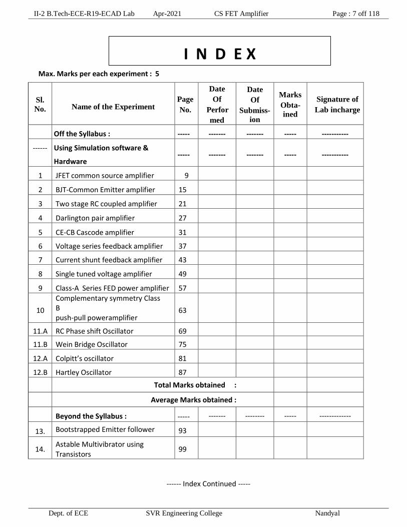
II-2 B.Tech-ECE-R19-ECAD Lab Apr-2021 CS FET Amplifier Page : 7 off 118
Dept. of ECE SVR Engineering College Nandyal
Max. Marks per each experiment : 5
Sl.
No. Name of the Experiment Page
No.
Date
Of
Perfor
med
Date
Of
Submiss-
ion
Marks
Obta-
ined
Signature of
Lab incharge
Off the Syllabus : ----- ------- ------- ----- -----------
------ Using Simulation software &
Hardware ----- ------- ------- ----- -----------
1 JFET common source amplifier 9
2 BJT-Common Emitter amplifier 15
3 Two stage RC coupled amplifier 21
4 Darlington pair amplifier 27
5 CE-CB Cascode amplifier 31
6 Voltage series feedback amplifier 37
7 Current shunt feedback amplifier 43
8 Single tuned voltage amplifier 49
9 Class-A Series FED power amplifier 57
10
Complementary symmetry Class B push-pull power amplifier
63
11.A RC Phase shift Oscillator 69
11.B Wein Bridge Oscillator 75
12.A Colpitt’s oscillator 81
12.B Hartley Oscillator 87
Total Marks obtained :
Average Marks obtained :
Beyond the Syllabus : ----- ------- -------- ----- -------------
13. Bootstrapped Emitter follower 93
14. Astable Multivibrator using Transistors
99
------ Index Continued -----
I N D E X
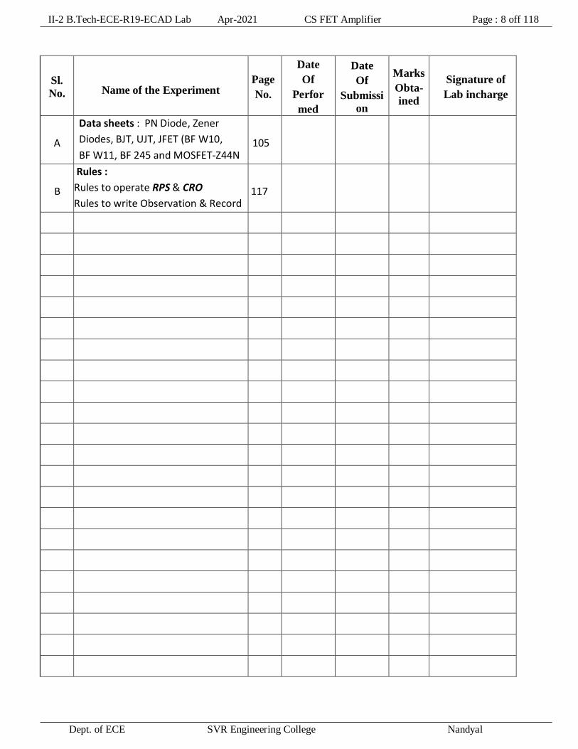
II-2 B.Tech-ECE-R19-ECAD Lab Apr-2021 CS FET Amplifier Page : 8 off 118
Dept. of ECE SVR Engineering College Nandyal
Sl.
No. Name of the Experiment Page
No.
Date
Of
Perfor
med
Date
Of
Submissi
on
Marks
Obta-
ined
Signature of
Lab incharge
A
Data sheets : PN Diode, Zener
Diodes, BJT, UJT, JFET (BF W10,
BF W11, BF 245 and MOSFET-Z44N 105
B
Rules :
Rules to operate RPS & CRO
Rules to write Observation & Record 117

II-2 B.Tech-ECE-R19-ECAD Lab Apr-2021 CS FET Amplifier Page : 9 off 118
Dept. of ECE SVR Engineering College Nandyal
AIM :
1). To obtain the frequency response of Common Source FET amplifier using Software and
Hardware 2). To calculate the band width of this amplifier.
APPARATUS :
Software :
1. System ------- 1 No.
2. Multisim software Hardware :
1). Function generator(FG)
2). Cathode Ray Oscilloscope(CRO)
3). Regulated Power Supply (RPS) :
4). Probes
5). Bread board
6). Connecting wires :
Dual channel, (0-30)V, 1A
-------------
-------------
-------------
-------------
-------------
-------------
1 No.
1 No.
1 No.
1 No.
1 No.
A few Nos.
COMPONENTS :
1). Transistor BF 245 / BF W11 ------------- 1 No.
2) Carbon fixed resistors a). 1.8KΩ, ½W ------------- 1 No.
b). 2.2KΩ , ½W ------------- 2 No.
c). 100KΩ , ½W ------------- 1 No.
3). Capacitors a). 0.22µF ------------- 2 No. b). 33µF ------------- 1 No.
THEORY :
Small signal amplifiers can also be made using Field Effect Transistors. These devices have the
advantage over bipolar transistors of having an extremely high input impedance along with a low noise
output making them ideal for use in amplifier circuits that have very small input signals.
The design of an amplifier circuit based around a junction field effect transistor or “JFET”, (N-
channel FET for this tutorial) or even a metal oxide silicon FET or “MOSFET” is exactly the same principle
as that for the bipolar transistor circuit used for a Class A amplifier circuit we looked at in the previous
tutorial.
Firstly, a suitable quiescent point or “Q-point” needs to be found for the correct biasing of the JFET
amplifier circuit with single amplifier configurations of Common-source (CS), Common-drain (CD) or
Source-follower (SF) and the Common-gate (CG) available for most FET devices.
Common Source JFET Amplifier as this is the most widely used JFET amplifier design.
The amplifier circuit consists of an N-channel JFET, but the device could also be an equivalent N-
channel depletion-mode MOSFET as the circuit diagram would be the same just a change in the FET,
connected in a common source configuration. The JFET gate voltage Vg is biased through the potential
divider network set up by resistors R1 and R2 and is biased to operate within its saturation region .
The junction FET takes virtually no input gate current allowing the gate to be treated as an open circuit. Then
no input characteristics curves are required.
Experiment No. : 1 Date :
Name of the Experiment : FET - COMMON SOURCE (CS) AMPLIFIER
II-2 B.Tech-ECE-R19-ECAD Lab Apr-2021 CS FET Amplifier Page : 10 off 118
Dept. of ECE SVR Engineering College Nandyal
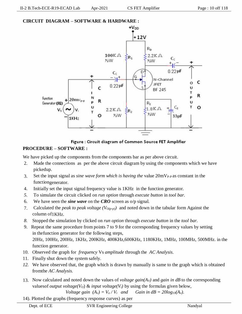
CIRCUIT DIAGRAM – SOFTWARE & HARDWARE :
PROCEDURE – SOFTWARE :
We have picked up the components from the components bar as per above circuit.
2. Made the connections as per the above circuit diagram by using the components which we have
picked up.
3. Set the input signal as sine wave form which is having the value 20mVP-P as constant in the
function generator.
4. Initially set the input signal frequency value is 1KHz in the function generator.
5. To simulate the circuit clicked on run option through execute button in tool bar.
6. We have seen the sine wave on the CRO screen as o/p signal.
7. Calculated the peak to peak voltage (VO(p-p)) and noted down in the tabular form Against the
column of 1KHz.
8. Stopped the simulation by clicked on run option through execute button in the tool bar.
9. Repeat the same procedure from points 7 to 9 for the corresponding frequency values by setting
in the function generator for the following steps,
20Hz, 100Hz, 200Hz, 1KHz, 200KHz, 400KHz,600KHz, 1180KHz, 1MHz, 100MHz, 500MHz. in the
function generator.
10. Observed the graph for frequency Vs amplitude through the AC Analysis.
11. Finally shut down the system safely.
12. We have observed that, the graph which is drawn by manually is same to the graph which is obtained
from the AC Analysis.
13. Now calculated and noted down the values of voltage gain(AV) and gain in dB to the corresponding
values of output voltage(VO) & input voltage(Vi) by using the formulas given below,
Voltage gain (Av) = Vo / Vi and Gain in dB = 20log10(Av).
14). Plotted the graphs (frequency response curves) as per

II-2 B.Tech-ECE-R19-ECAD Lab Apr-2021 CS FET Amplifier Page : 11 off 118
Dept. of ECE SVR Engineering College Nandyal
below a). frequency on X-axis & gain in dB on Y-
axis.
PROCEDURE – HARDWARE :
1). Connected the circuit as per the circuit diagram.
2). Then switched ON the function generator and CRO; but don’t switched ON the
RPS. 3). Now Kept the AC/GND/DC switch is at AC position.
4). Initially kept the 1KHz. frequency by varying the frequency control in the function generator.
5). Now applied the peak to peak amplitude of a sine wave is of 20mVp-p by varying the amplitude
control in the function generator through observing in the CRO.
6). Kept this input value as 20mVp-p constant up to the completion of the experiment
Otherwise the wrong output would occurred.
7). Now switched ON the RPS and set the 10V in it i.e. VCC = 10V.
8). Varied the different frequency steps of 20Hz, 100Hz, 200Hz, 1KHz, 200KHz, 400KHz,
600KHz, 1180KHz,1MHz.
by adjusted the frequency control in the function generator and noted down the corresponding
values of output signal i.e. peak to peak amplitude of sine wave by observing in the CRO.
9). Now switched OFF the RPS, function generator and CRO.
10). Then calculated the voltage gain AV = VO/Vi & gain in dB = 20log10(AV) and noted down the values
in the specified columns of the tabular column.
11). Plotted the graphs (frequency response curves) as per
below, a). frequency on X-axis & gain in dB on Y-
axis.
b). frequency on X-axis & voltage gain on Y-axis.
12) Calculated the band width from the above two (frequency response curves) graphs
by using the formula f2 – f1 which is given under the heading of parameters.
TABULAR COLUMNS – SOFTWARE & HARDWARE :
Input Voltage (Vi) = 20 mVP-P is constant for all
readings For Software : For Hardware :
Sl. Frequ- Output Voltage Gain in Frequ- Output Voltage Gain in
No. ency Voltage gain dB = ency Voltage gain dB =
In (VO) In AV= 20log10 In (VO)In AV= 20log10
Hz/KHz. mVolts. Vo/Vi (AV) Hz/KHz. mVolts. Vo/Vi (AV)
1 20 Hz.
2 100 Hz.
3 200 Hz.
5 1 KHz.
6 200KHz.
7 400KHz.
8 600KHz.
To be continued in next page

II-2 B.Tech-ECE-R19-ECAD Lab Apr-2021 CS FET Amplifier Page : 12 off 118
Dept. of ECE SVR Engineering College Nandyal
Sl. Frequ- Output Voltage Gain in Frequ- Output Voltage Gain in
No. ency Voltage gain dB = ency Voltage gain dB =
In (VO) In AV= 20log10 In (VO)In AV= 20log10
Hz/KHz. mVolts. Vo/Vi (AV) Hz/KHz. mVolts. Vo/Vi (AV)
9 800KHz.
10 1 MHz.
11 100 MHz ------- ------- ------- -------
12 500MHz. ------- ------- ------- -------
EXPECTED GRAPHS – SOFTWARE & HARDWRE :
A). Frequency response curve B). Frequency response curve
For frequency verses gain in dB. For frequency verses voltage gain.
PARAMETERS – SOFTWARE & HARDWARE :
1). Band width of frequency response
curve for frequency verses gain in dB.
= f2 –
f1
2) Band width of frequency response
curve for frequency verses voltage gain
= f2 – f1
RESULT – SOFTWARE & HARDWARE :
We have obtained the frequency response curves of Common Source FET Amplifier (CSFET)
for frequency verses gain in dB & frequency verses voltage gain and calculated the band width of both
of them. The band width values are given below,
1). Band width of frequency response curve for frequency verses gain in dB. =
2) Band width of frequency response curve for frequency verses voltage gain =

II-2 B.Tech-ECE-R19-ECAD Lab Apr-2021 CS FET Amplifier Page : 13 off 118
Dept. of ECE SVR Engineering College Nandyal
VIVA VOICE QUESTIONS:
1. What is the Difference between BJT and FET?
2. What is Amplifier?
3. What is Band Width?
4. What are the applications of CS FET Amplifier?
5. FET is which controlled device?
6. Mention FET characteristics.
7. What are the configurations of FET?
8. What are the classifications of FET?
9. Which configuration mostly used in FET?
10. What is dB?

II-2 B.Tech-ECE-R19-ECAD Lab Apr-2021 CE Amplifier Page : 15 off 118
Dept. of ECE SVR Engineering College Nandyal
AIM :
1). To obtain the frequency response of Common Emitter amplifier using Hardware and
Software 2). To calculate the band width of this amplifier.
APPARATUS :
Software :
1. System 1 No.
2. Multisim software
Hardware :
1). Function generator(FG)
2). Cathode Ray Oscilloscope(CRO)
3). Regulated Power Supply (RPS) :
4). Probes
5). Bread board
6). Connecting wires :
(0-30)V, 1A
Dual channel
-------- 1 No.
-------- 1 No.
-------- 1 No.
-------- 1 No.
-------- 1 No.
-------- A few Nos.
COMPONENTS :
1). Transistor BC 547
-------- 1 No.
2) Carbon fixed resistors a). 47KΩ, ½W -------- 1 No.
b). 10KΩ , ½W -------- 1 No.
c). 4.7 KΩ , ½W -------- 1 No.
d). 1 KΩ , ½W -------- 1 No.
3). Capacitors a). 0.22µF -------- 2 No. b). 33µF -------- 1 No.
THEORY :
A transistor in which the emitter terminal is made common for both the input and the output circuit
connections is known as common emitter configuration. When this configuration is provided with the supply of
the alternating current (AC) and operated in between the both positive and the negative halves of the cycle in
order to generate the specific output signal is known as common emitter amplifier.
In this type of configuration the input is applied at the terminal base and the considered output is to be collected
across the term Voltage Gain
The ratio of the output voltage generated when the input voltage applied decides the voltage gain of the
common emitter amplifier.
Characteristics
The characteristics of the common emitter configuration amplifier configuration are as follows
The voltage gain value obtained for the common emitter amplifier is medium.
It also consists of the current gain in the medium range.
Because of both the voltage and the current gains the power gain value of this configuration is referred to be
high.
Experiment No. : 2 Date :
Name of the Experiment : BJT - COMMON EMITTER (CE) AMPLIFIER
II-2 B.Tech-ECE-R19-ECAD Lab Apr-2021 CE Amplifier Page : 16 off 118
Dept. of ECE SVR Engineering College Nandyal
There is some resistance value at the inputs as well as the output but in this configuration it is maintained at the
medium value.
Applications
1. These amplifiers are preferably used as the current amplifier than a voltage amplifier as it has more current
gain than the voltage gain.
2. In the radio frequency circuitry this configuration is preferred.
3. For the lower values of noise and its amplification this configuration is preferred.
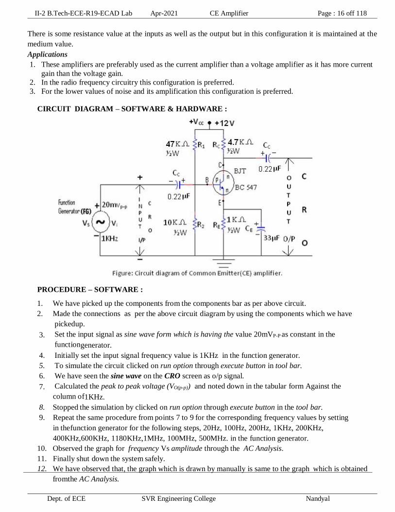
CIRCUIT DIAGRAM – SOFTWARE & HARDWARE :
PROCEDURE – SOFTWARE :
1. We have picked up the components from the components bar as per above circuit.
2. Made the connections as per the above circuit diagram by using the components which we have
picked up.
3. Set the input signal as sine wave form which is having the value 20mVP-P as constant in the
function generator.
4. Initially set the input signal frequency value is 1KHz in the function generator.
5. To simulate the circuit clicked on run option through execute button in tool bar.
6. We have seen the sine wave on the CRO screen as o/p signal.
7. Calculated the peak to peak voltage (VO(p-p)) and noted down in the tabular form Against the
column of 1KHz.
8. Stopped the simulation by clicked on run option through execute button in the tool bar.
9. Repeat the same procedure from points 7 to 9 for the corresponding frequency values by setting
in the function generator for the following steps, 20Hz, 100Hz, 200Hz, 1KHz, 200KHz,
400KHz,600KHz, 1180KHz,1MHz, 100MHz, 500MHz. in the function generator.
10. Observed the graph for frequency Vs amplitude through the AC Analysis.
11. Finally shut down the system safely.
12. We have observed that, the graph which is drawn by manually is same to the graph which is obtained
from the AC Analysis.

II-2 B.Tech-ECE-R19-ECAD Lab Apr-2021 CE Amplifier Page : 17 off 118
Dept. of ECE SVR Engineering College Nandyal
13. Now calculated and noted down the values of voltage gain(AV) and gain in dB to the corresponding
values of output voltage(VO) & input voltage(Vi) by using the formulas given below,
Voltage gain (Av) = Vo / Vi and Gain in dB = 20log10(Av).
14). Plotted the graphs (frequency response curves) as per below
a). frequency on X-axis & gain in dB on Y-axis.
b). frequency on X-axis & voltage gain on Y-axis.
PROCEDURE – HARDWARE :
1). Connected the circuit as per the circuit diagram.
2). Then switched ON the function generator and CRO; but don’t switched ON the
RPS. 3). Now Kept the AC/GND/DC switch is at AC position.
4). Initially kept the 1KHz. frequency by varying the frequency control in the function generator.
5). Now applied the peak to peak amplitude of a sine wave is of 20mVp-p by varying the amplitude
control in the function generator through observing in the CRO.
6). Kept this input value as 20mVp-p constant up to the completion of the experiment
Otherwise the wrong output would occurred.
7). Now switched ON the RPS and set the 10V in it i.e. VCC = 10V.
8). Varied the different frequency steps of 20Hz, 100Hz, 200Hz, 1KHz, 200KHz, 400KHz,
600KHz, 1180KHz,1MHz. by adjusted the frequency control in the function generator and
noted down the corresponding values of
output signal i.e. peak to peak amplitude of sine wave by observing in the CRO.
9). Now switched OFF the RPS, function generator and CRO.
10). Then calculated the voltage gain AV = VO/Vi & gain in dB = 20log10(AV) and noted down the values
in the specified columns of the tabular column.
11). Plotted the graphs (frequency response curves) as per below,
a). frequency on X-axis & gain in dB on Y-axis.
b). frequency on X-axis & voltage gain on Y-axis.
12) Calculated the band width from the above two (frequency response curves) graphs
by using the formula f2 – f1 which is given under the heading of parameters.
TABULAR COLUMNS :
Input Voltage (Vi) = 20 mVP-P (0.02V) is constant for all readings.
For Software : For Hardware :
Sl.No. Frequ- Output Voltage Gain in Frequ- Output Voltag Gain in
ency Voltage gain dB = ency Voltage e dB =
In (VO) In AV= 20log10 In (VO)In gain 20log10
Hz/KHz. mVolts. Vo/Vi (AV) Hz/KHz. mVolts. AV= (AV) Vo/Vi
1 20 Hz.
2 100 Hz.
3 200 Hz.
5 1 KHz.
To continued in next page
II-2 B.Tech-ECE-R19-ECAD Lab Apr-2021 CE Amplifier Page : 18 off 118
Dept. of ECE SVR Engineering College Nandyal
Sl.No. Frequ- Output Voltage Gain in Frequ- Output Voltag Gain in
ency Voltage gain dB = ency Voltage e dB =
In (VO) In AV= 20log10 In (VO)In gain 20log10
Hz/KHz. mVolts. Vo/Vi (AV) Hz/KHz. mVolts. AV= (AV)
Vo/Vi
6 200KHz.
7 400KHz.
8 600KHz.
9 1180KHz.
10 1 MHz.
11 100 MHz ------- ------- ------- -------
12 500MHz. ------- ------- ------- -------
EXPECTED GRAPHS – SOFTWARE & HARDWARE :
A). Frequency response curve B). Frequency response curve
For frequency verses gain in dB. For frequency verses voltage gain.
PARAMETERS – SOFTWARE & HARDWARE :
1). Band width of frequency response curve for
frequency verses gain in dB. = f2 – f1 =
2) Band width of frequency response curve for
frequency verses voltage gain = f2 – f1 =
RESULT –SOFTWARE & HARDWARE :
We have obtained the frequency response curves of Common Emitter Amplifier (CE)
for frequency verses gain in dB & frequency verses voltage gain and calculated the band width of both of
them. The band width values are given below,
1). Band width of frequency response curve for frequency verses gain in dB. =
2) Band width of frequency response curve for frequency verses voltage gain =

II-2 B.Tech-ECE-R19-ECAD Lab Apr-2021 CE Amplifier Page : 19 off 118
Dept. of ECE SVR Engineering College Nandyal
VIVA VOICE QUESTIONS:
1. What is BJT?
2. What are the applications of BJT?
3. What is Early Effect?
4. Define alpha and beta DC amplification factors of BJT.
5. Briefly explain reach through effect.
6. Draw the symbols for BJT.
7. Explain the transistor operation with the help of four regions
8. Explain base width modulation of a transistor
9. Compare CB,CE, CC configurations of a transistor.
10. A transistor has CE current gain of 100. If the collector is 40 mA. What is the value of emitter current?[

II-2 B.Tech-ECE-R19-ECAD Lab Apr-2021 Two Stg. RC Cpld Amplifie Page : 21 off 118
Dept. of ECE SVR Engineering College Nandyal
AIM :
To verify / plot the frequency response curve and to find the band width. of a two stage RC
coupled Amplifier using software and hardware
APPARATUS :
Software :
1. System 1 No.
2. Multisim software
Hardware :
1). Function generator(FG) -------- 1 No.
2). Cathode Ray Oscilloscope(CRO)
3). Regulated Power Supply (RPS) :
4). Probes
5). Bread board
6). Connecting wires :
(0-30)V, 1A
Dual channel
-------- 1 No.
-------- 1 No.
-------- 1 No.
-------- 1 No.
-------- A few Nos.
COMPONENTS :
1). Transistor BC 547 --------------------------------------------------------------------- 2 No.
2) Carbon fixed resistors a). 47KΩ, ½W -------- 2 No.
b). 10KΩ , ½W -------- 2 No.
c). 4.7 KΩ , ½W -------- 2 No.
d). 1 KΩ , ½W -------- 2 No.
3). Capacitors a). 0.22µF -------- 4 No. b). 33µF -------- 2 No.
THEORY :
RC coupling is the most widely used method of coupling in multistage amplifiers. ... In this case the
resistance R is the resistor connected at the collector terminal and the capacitor C is connected in between the
amplifiers. It is also called a blocking capacitor, since it will block DC voltage.
Advantages :
The following are the advantages of RC coupled amplifier. The frequency response of RC amplifier
provides constant gain over a wide frequency range, hence most suitable for audio applications. The circuit is
simple and has lower cost because it employs resistors and capacitors which are cheap.
Gain :
The gain of an amplifier is increased by connecting the amplifiers in cascaded manner. The output of one
stage is connected to the input of next stage through the coupling capacitor.It increases the overall gain of the
amplifier and decreases the overall bandwidth of the amplifier.
Applications :
Optical Fiber Communications. Public address systems as pre-amplifiers. Controllers. Radio or TV
Receivers as small signal amplifiers.2
Experiment No. : 03 Date :
Name of the Experiment : TWO STAGE RC COUPLED AMPLIFIER
II-2 B.Tech-ECE-R19-ECAD Lab Apr-2021 Two Stg. RC Cpld Amplifie Page : 22 off 118
Dept. of ECE SVR Engineering College Nandyal
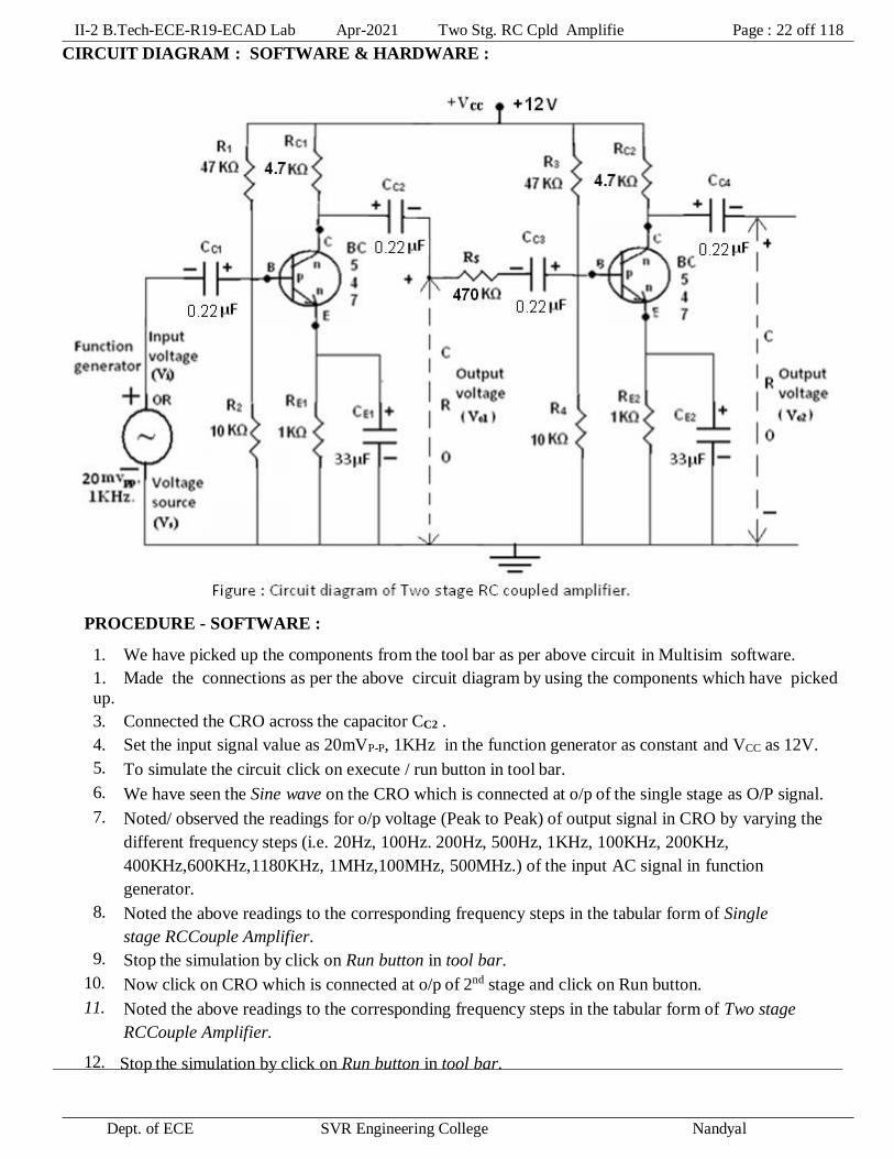
CIRCUIT DIAGRAM : SOFTWARE & HARDWARE :
PROCEDURE - SOFTWARE :
1. We have picked up the components from the tool bar as per above circuit in Multisim software.
1. Made the connections as per the above circuit diagram by using the components which have picked
up.
3. Connected the CRO across the capacitor CC2 .
4. Set the input signal value as 20mVP-P, 1KHz in the function generator as constant and VCC as 12V.
5. To simulate the circuit click on execute / run button in tool bar.
6. We have seen the Sine wave on the CRO which is connected at o/p of the single stage as O/P signal.
7. Noted/ observed the readings for o/p voltage (Peak to Peak) of output signal in CRO by varying the
different frequency steps (i.e. 20Hz, 100Hz. 200Hz, 500Hz, 1KHz, 100KHz, 200KHz,
400KHz,600KHz, 1180KHz, 1MHz,100MHz, 500MHz.) of the input AC signal in function
generator.
8. Noted the above readings to the corresponding frequency steps in the tabular form of Single
stage RC Couple Amplifier.
9. Stop the simulation by click on Run button in tool bar.
10. Now click on CRO which is connected at o/p of 2nd stage and click on Run button.
11. Noted the above readings to the corresponding frequency steps in the tabular form of Two stage
RC Couple Amplifier.
12. Stop the simulation by click on Run button in tool bar.

II-2 B.Tech-ECE-R19-ECAD Lab Apr-2021 Two Stg. RC Cpld Amplifie Page : 23 off 118
Dept. of ECE SVR Engineering College Nandyal
13. Observed the graph frequency Vs amplitude through the AC Analysis for Two stage RC
Coupled Amplifier.
14. Shut down the system safely.
15. Calculated and noted the Voltage gain by using the formula of Vo / Vi and Gain in dB by using the
formula of 20log10(AV) in the tabular form of both Single stage and Two stage RC Coupled
amplifiers.
16. Drawn the graph for which the frequency on X-axis and Gain in dB on Y-axis for both RC
Coupled Amplifier circuits..
17. We have calculated the bandwidth of both RC Coupled amplifiers from that graph as per given
formula,
Band width for Single stage RC Coupled Amplifier (BW) = f2
– f1 Band width for Two stage RC Coupled Amplifier (BW) =
f4 –f3
18. We have observed that, the graph which is drawn by manually is same to the graph which is obtained
from the AC Analysis for both RC coupled amplifiers.
PROCEDURE - HARDWARE :
1. We have connected the circuit as per the circuit diagram which is shown above.
2. Initially connected the probe across the function generator as per shown in the circuit diagram to
set the input signal.
1. Switched ON the CRO and function generator.
2. Applied the input signal as sine wave form having the values of 20mP-P 1KHz.from the function
generator by observing in the CRO.
3. Removed the probe from that place and connected it across the CC2 to observe the output of single
stage.
4. Switched ON the RPS and kept the +12V as VCC.
5. Kept the amplitude of the input signal as constant as 20mVp-p for all frequency steps.
6. Noted down the values of output voltage in terms of peak to peak voltages by varying the
different frequency steps in the function generator which are given below,
20Hz, 100Hz., 200Hz., 500Hz, 1KHz, 100KHz, 200KHz, 400KHz, 600KHz, 1180KHz, 1MHz.
7. The above readings noted in the tabular form of single stage RC coupled amplifier.
8. Disconnect the probe from CC2 and reconnected it across CC4 to observe the output of second stage.
9. Repeat the same procedure from the step 6 to 8 for tabular form of Two stage RC Coupled Amplifier.
10. Now calculated and noted down the values in the tabular form of single stage RC Coupled
Amplifier as per given below,
a). Voltage gain (Av) = Vo / Vi and Gain in dB = 20log10(Av).
b). Plotted the graph between frequency on X- axis and gain in dB on Y-
axis. c). Band width from the graph by using the formula- Band width =
f2 – f1
11. Now calculated and noted down the values in the tabular form of Two stage RC Coupled
Amplifier as per given below,
a). Voltage gain (Av) = Vo / Vi and Gain in dB = 20log10(Av).
b). Plotted the graph between frequency on X- axis and gain in dB on Y-
axis. c). Band width from the graph by using the formula- Band width =
f4 – f3
II-2 B.Tech-ECE-R19-ECAD Lab Apr-2021 Two Stg. RC Cpld Amplifie Page : 24 off 118
Dept. of ECE SVR Engineering College Nandyal
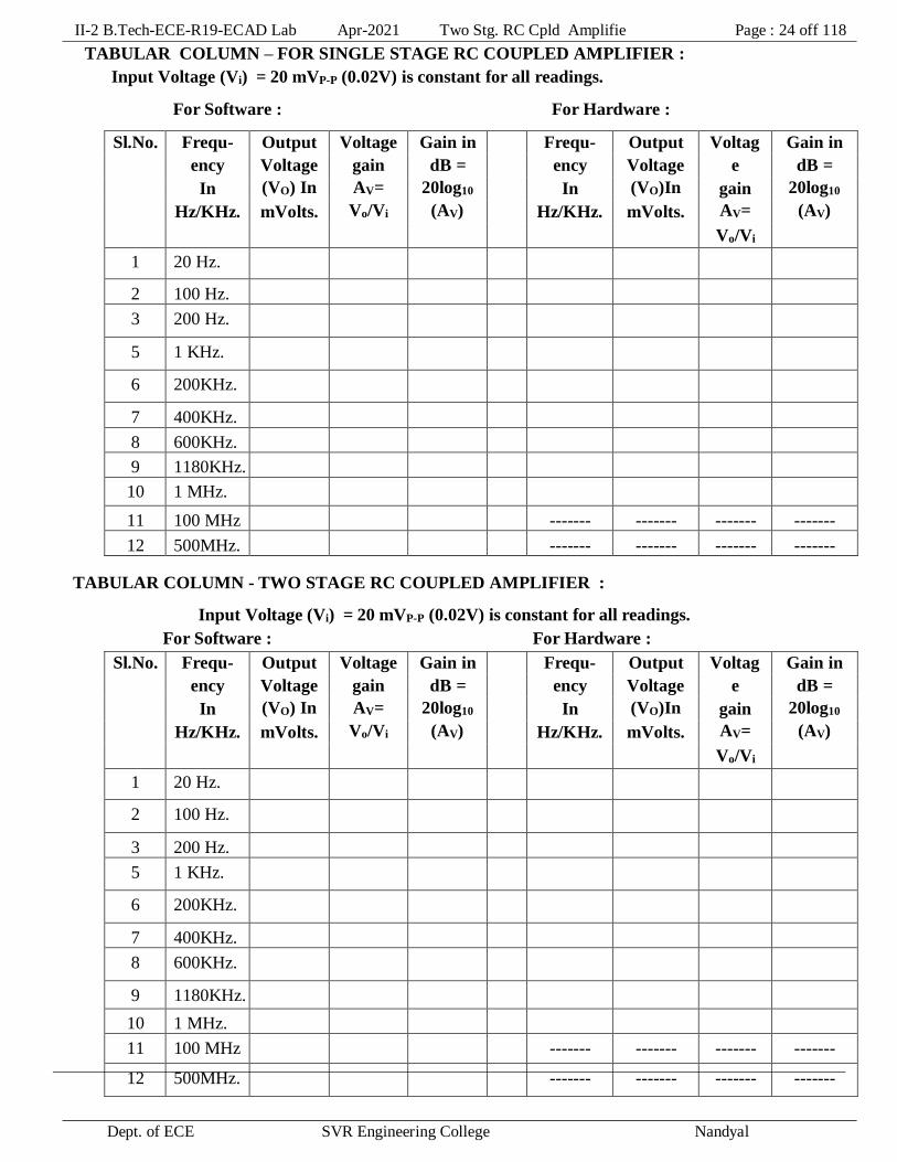
TABULAR COLUMN – FOR SINGLE STAGE RC COUPLED AMPLIFIER :
Input Voltage (Vi) = 20 mVP-P (0.02V) is constant for all readings.
For Software : For Hardware :
Sl.No. Frequ- Output Voltage Gain in Frequ- Output Voltag Gain in
ency Voltage gain dB = ency Voltage e dB =
In (VO) In AV= 20log10 In (VO)In gain 20log10
Hz/KHz. mVolts. Vo/Vi (AV) Hz/KHz. mVolts. AV= (AV)
Vo/Vi
1 20 Hz.
2 100 Hz.
3 200 Hz.
5 1 KHz.
6 200KHz.
7 400KHz.
8 600KHz.
9 1180KHz.
10 1 MHz.
11 100 MHz ------- ------- ------- -------
12 500MHz. ------- ------- ------- -------
TABULAR COLUMN - TWO STAGE RC COUPLED AMPLIFIER :
Input Voltage (Vi) = 20 mVP-P (0.02V) is constant for all readings.
For Software : For Hardware :
Sl.No. Frequ- Output Voltage Gain in Frequ- Output Voltag Gain in
ency Voltage gain dB = ency Voltage e dB =
In (VO) In AV= 20log10 In (VO)In gain 20log10
Hz/KHz. mVolts. Vo/Vi (AV) Hz/KHz. mVolts. AV= (AV)
Vo/Vi
1 20 Hz.
2 100 Hz.
3 200 Hz.
5 1 KHz.
6 200KHz.
7 400KHz.
8 600KHz.
9 1180KHz.
10 1 MHz.
11 100 MHz ------- ------- ------- -------
12 500MHz. ------- ------- ------- -------

II-2 B.Tech-ECE-R19-ECAD Lab Apr-2021 Two Stg. RC Cpld Amplifie Page : 25 off 118
Dept. of ECE SVR Engineering College Nandyal
EXPECTED WAVEFORM – SOFTWARE & HARDWARE :
I have got the Sine wave form on the CRO as output signal for single stage as well as for Two stage
RC Coupled Amplifiers which is shown below,
EXPECTED GRAPH – SOFTWARE & HARDWARE :
The following graph shows the frequency response curves of both Single stage & Two stage RC coupled
Amplifiers.
CALCULATIONS – SOFTWARE & HARDWARE :
1). Band width “single stage RC coupled amplifier = f2 – f1 =
2). Band width “two stage RC coupled amplifier = f4 – f3 =
CONCLUSION – SOFTWARE & HARDWARE :
1. I have observed that
a). The bandwidth of Two stage RC coupled amplifier is less as compared to Single stage RC
coupled amplifier and
b). The gain of Two stage RC coupled amplifier is more as compared to Single stage RC coupled
amplifier
RESULT – SOFTWARE & HARDWARE :
I verified / drawn the frequency response curve and found the bandwidth values of a single stage &
two stage RC coupled amplifiers. The band width values are,
1). Band width of single stage RC coupled amplifier =
2). Band width of two stage RC coupled amplifier =

II-2 B.Tech-ECE-R19-ECAD Lab Apr-2021 Two Stg. RC Cpld Amplifie Page : 26 off 118
Dept. of ECE SVR Engineering College Nandyal
VIVA VOCE QUESTIONS :
1. Applications of Darlington pair Amplifier.
2. Applications of Multi stage amplifiers?
3. Mention Advantages of Multistage Amplifiers.
4. What is Band Width?
5. What is Frequency Response?
6. Need for multi stage amplifier?
7. What are the different coupling schemes?
8. Applications of Multi stage amplifiers?
9. Mention Advantages of Multistage Amplifiers.
10. What is Band Width?
II-2 B.Tech-ECE-R19-ECAD Lab Apr-2021 Darlington Pair Amplifie Page : 27 off 118
Dept. of ECE SVR Engineering College Nandyal
AIM :
To obtain the frequency response curve of Darlington pair amplifier using software & hardware
APPARATUS :
Software :
1. System
2. Multisim software
Hardware : 1). Transisitor
2). Resistors
a). BC547 NPN
a). 47K Ω
b). 10 K Ω
---------
--------
--------
2 No.
2 No.
2 No.
d). 1 K Ω -------- 2 No.
3). Capacitors a). 0.22 µF -------- 3 No.
THEORY :
Darlington Pair amplifier circuit is a connection of two transistors which acts as a single unit with
overall current gain equal to the multiplication of the individual current gains of the transistors. Darlington
pair transistor amplifier circuit is very popular in electronics. Clearly, it is an Amplifier circuit. In this
article, we are going to discuss the theory and the applications of Darlington pair amplifier.
The current gain of Darlington pair amplifier is almost equal to the product between the current gains of
individual transistors. If _\beta 1β1 and _\beta 2β2 be the current gains of individual transistors then overall
current gain of Darlington pair amplifier = β1β2.
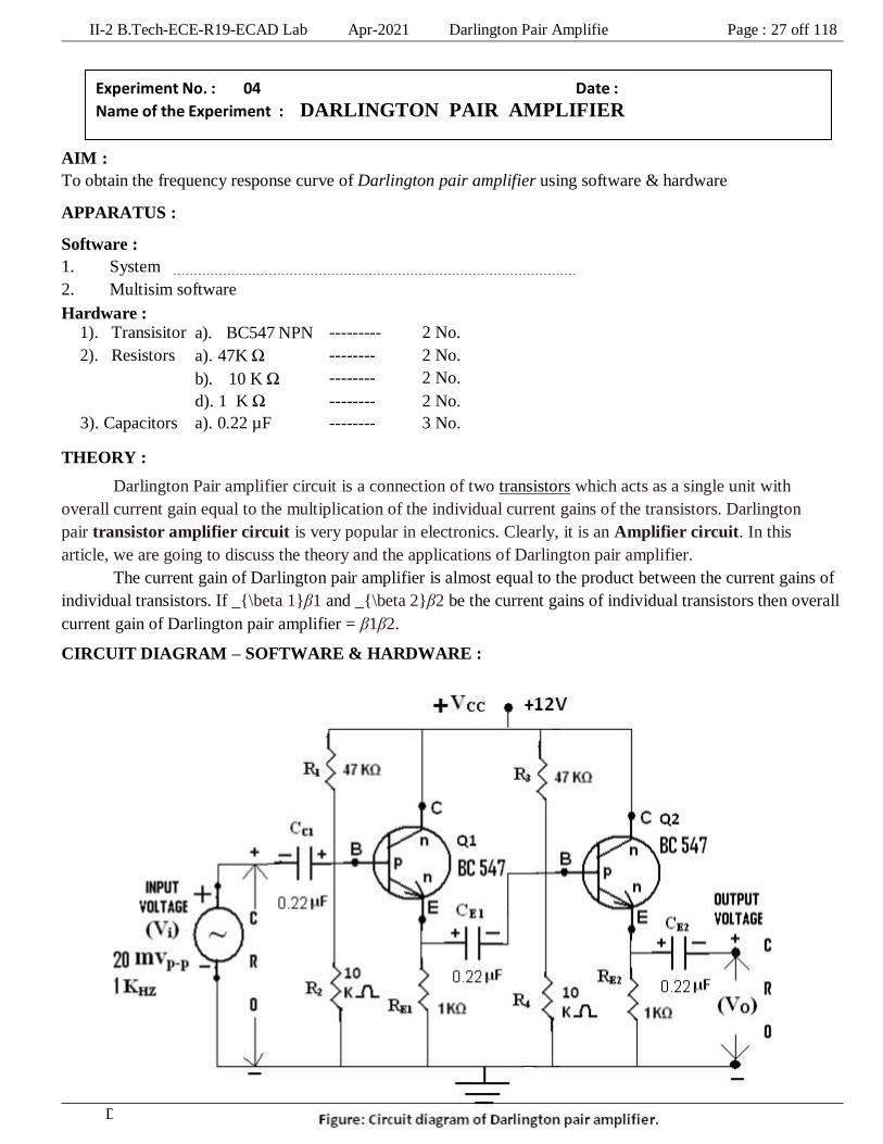
CIRCUIT DIAGRAM – SOFTWARE & HARDWARE :
Experiment No. : 04 Date :
Name of the Experiment : DARLINGTON PAIR AMPLIFIER
II-2 B.Tech-ECE-R19-ECAD Lab Apr-2021 Darlington Pair Amplifie Page : 28 off 118
Dept. of ECE SVR Engineering College Nandyal
PROCEDURE – SOFTWARE :
1. We have picked up the components from the components bar as per above circuit.
2. Made the connections as per the above circuit diagram by using the components which we have
picked up.
3. Connected the CRO across the capacitor CE2 of second stage.
4. Set the input signal as sine wave form which is having the value 20mVP-P as constant in the
function generator.
5. Initially set the input signal frequency value is 1KHz in the function generator.
6. To simulate the circuit clicked on run option through execute button in tool bar.
7. We have seen the sine wave on the CRO screen as o/p signal.
8. Calculated the peak to peak voltage (VO(p-p)) and noted down in the tabular form Against the 3
column of 1KHz.
9. Stopped the simulation by clicked on run option through execute button in the tool bar.
10. Repeated the same procedure from points 6 to 9 for the corresponding frequency values by setting
in the function generator for the following steps,
20Hz, 100Hz., 200Hz., 500Hz, 1KHz, 200KHz, 400KHz,600KHz, 1180KHz, 1MHz, 100MHz,
500MHz.
in the function generator.
11. Finally shut down the system safely.
12. Now calculated and noted down the values of voltage gain(AV) and gain in dB to the corresponding
values of output voltage(VO) & input voltage(Vi) by using the formulas given below,
Voltage gain (Av) = Vo / Vi and Gain in dB = 20log10(Av).
PROCEDURE – HARDWARE :
1. We have connected the circuit as per the circuit diagram which is shown above.
2. Initially connected the probe across the function generator as per shown in the circuit diagram to
set the input signal.
3. Switched ON the CRO and function generator.
4. Applied the input signal as sine wave form of 20mp-p, 1KHz.from the function generator by
observing in the CRO.
5. Later removed the probe from that place and connected it across the capacitor CE3 to observe the output.
6. Switched ON the RPS and kept the 12V as VCC.
7. Kept the amplitude of the input signal as constant as 20mVp-p for all frequency steps.
8. Noted down the values output voltage of output signal in terms of peak to peak voltages by varying the
different frequency steps in the function generator which are given below,
20Hz, 100Hz., 200Hz., 500Hz, 1KHz, 100KHz, 200KHz, 400KHz, 600KHz, 1180KHz, 1MHz.
9. Repeated the same procedure for point 8 for corresponding frequency values.
10. Now calculated and noted down the values of voltage gain(AV) and gain in dB to the corresponding
values of output voltage(VO) & input voltage(Vi) by using the formulas given below,
Voltage gain (Av) = Vo / Vi and Gain in dB = 20log10(Av).
TABULAR COLUMN :
Input Voltage (Vi) = 20 mVP-P (0.02V) is constant for all readings.
For Software : For Hardware :

II-2 B.Tech-ECE-R19-ECAD Lab Apr-2021 Darlington Pair Amplifie Page : 29 off 118
Dept. of ECE SVR Engineering College Nandyal
Sl.No. Frequ- Output Voltage Gain in Frequ- Output Voltag Gain in
ency Voltage gain dB = ency Voltage e dB =
In (VO) In AV= 20log10 In (VO)In gain 20log10
Hz/KHz. mVolts. Vo/Vi (AV) Hz/KHz. mVolts. AV= (AV)
Vo/Vi
1 20 Hz.
2 100 Hz.
3 200 Hz.
4 1 KHz.
5 200KHz.
6 400KHz.
7 600KHz.
8 1180KHz.
9 1 MHz.
10 100 MHz ------- ------- ------- -------
11 500MHz. ------- ------- ------- -------
EXPECTED GRAPH – SOFTWARE & HARDWARE :
Note : We can’t draw the graph and could not find the band width for this experiment, because there is
no amplification.
CONCLUSSION :
We have formed the circuit of Darlington pair amplifier by connected two common collector
amplifiers in two stages. The input impedance of two stage common collector amplifier i.e. Darlington pair
amplifier is very high as compared to single stage common collector amplifier. Due to this reason only the
voltage gain of Darlington pair amplifier is less than as compared to single stage common collector amplifier.
RESULT – SOFTWARE & HARDWARE :
I have obtained the voltage gain and gain in db at different frequencies of a Darlington pair
amplifier.

II-2 B.Tech-ECE-R19-ECAD Lab Apr-2021 Darlington Pair Amplifie Page : 30 off 118
Dept. of ECE SVR Engineering College Nandyal
VIVA VOICE QUESTIONS:
1. Applications of Darlington pair Amplifier.
2. Applications of Multi stage amplifiers?
3. Mention Advantages of Multistage Amplifiers.
4. What is Band Width?
5. What is Frequency Response?
6. Compare CB,CE, CC configurations of a transistor
7. Explain the transistor operation with the help of four regions
8. What is cascade Amplifier?
9. Explain base width modulation of a transistor
10. Which Amplifier is having CC-CC configuration?

II-2 B.Tech-ECE-R19-ECAD Lab Apr-2021 CE-CB Cascode Amplifie Page : 31 off 118
Dept. of ECE SVR Engineering College Nandyal
AIM :
1). To obtain the frequency response of CE – CB cascade amplifier using Software and Hardware
2). To calculate the band width of this amplifier.
APPARATUS :
Software :
1. System 1 No.
2. Multisim software
Hardware :
1). Function generator(FG) --------------------------------------------------------------- 1 No.
2). Cathode Ray Oscilloscope(CRO) ----------------------------------------------------- 1 No.
3). Regulated Power Supply (RPS) : (0-30)V, 1A Dual channel ---------- 1 No.
4). Probes ------------------------------------------------------------------------------------ 1 No.
5). Bread board ----------------------------------------------------------------------------- 1 No.
6). Connecting wires : ----------------------------------------------------------------------A few Nos.
COMPONENTS :
1). Transistor BC 547 ------------------------------------------------------------------------1 No.
2) Carbon fixed resistors a). 47KΩ, ½W -------- 1 No.
b). 40.2KΩ -------- 1 No.
c). 10KΩ , ½W -------- 1 No.
d). 6.8 KΩ , ½W -------- 1 No.
e). 4.7 KΩ , ½W -------- 1 No.
f). 1 KΩ , ½W -------- 1 No.
3). Capacitors g). 0.22µF -------- 3 No. h). 33µF -------- 1 No.
THEORY :
While the C-B (common-base) amplifier is known for wider bandwidth than the C-E (common-emitter)
configuration, the low input impedance (10s of Ω) of C-B is a limitation for many applications. The solution is
to precede the C-B stage by a low gain C-E stage which has moderately high input impedance (kΩs).
The stages are in a cascode configuration stacked in series, as opposed to cascaded for a standard
amplifier chain.
The key to understanding the wide bandwidth of the cascode configuration is the Miller effect. The
Miller effect is the multiplication of the bandwidth robbing collector-base capacitance by voltage gain Av.
Experiment No. : 05 Date :
Name of the Experiment : CE – CB - CASCODE AMPLIFIER

II-2 B.Tech-ECE-R19-ECAD Lab Apr-2021 CE-CB Cascode Amplifie Page : 32 off 118
Dept. of ECE SVR Engineering College Nandyal
CIRCUIT DIAGRAM – SOFTWARE & HARDWARE :
PROCEDURE – SOFTWARE :
1. We have picked up the components from the components bar as per above circuit.
2. Made the connections as per the above circuit diagram by using the components which we have
picked up.
3. Set the input signal as sine wave form which is having the value 20mVP-P as constant in the
function generator.
4. Initially set the input signal frequency value is 1KHz in the function generator.
5. To simulate the circuit clicked on run option through execute button in tool bar.
6. We have seen the sine wave on the CRO screen as o/p signal.
7. Calculated the peak to peak voltage (VO(p-p)) and noted down in the tabular form Against the
column of 1KHz.
8. Stopped the simulation by clicked on run option through execute button in the tool bar.
9. Repeat the same procedure from points 7 to 9 for the corresponding frequency values by setting
in the function generator for the following steps, 20Hz, 100Hz, 200Hz, 1KHz, 200KHz,
400KHz,600KHz, 1180KHz,1MHz, 100MHz, 500MHz. in the function generator.
10. Observed the graph for frequency Vs amplitude through the AC Analysis.
11. Finally shut down the system safely.
12. We have observed that, the graph which is drawn by manually is same to the graph which is obtained
from the AC Analysis.

II-2 B.Tech-ECE-R19-ECAD Lab Apr-2021 CE-CB Cascode Amplifie Page : 33 off 118
Dept. of ECE SVR Engineering College Nandyal
13. Now calculated and noted down the values of voltage gain(AV) and gain in dB to the corresponding
values of output voltage(VO) & input voltage(Vi) by using the formulas given below,
Voltage gain (Av) = Vo / Vi and Gain in dB = 20log10(Av).
14). Plotted the graphs (frequency response curves) as per below
a). frequency on X-axis & gain in dB on Y-axis.
b). frequency on X-axis & voltage gain on Y-axis.
PROCEDURE – HARDWARE :
1). Connected the circuit as per the circuit diagram.
2). Then switched ON the function generator and CRO; but don’t switched ON the RPS. 3). Now Kept the
AC/GND/DC switch is at AC position.
4). Initially kept the 1KHz. frequency by varying the frequency control in the function generator.
5). Now applied the peak to peak amplitude of a sine wave is of 20mVp-p by varying the amplitude control
In the function generator through observing in the CRO.
6). Kept this input value as 20mVp-p constant up to the completion of the experiment Otherwise
the wrong output would occurred.
7). Now switched ON the RPS and set the 10V in it i.e. VCC = 12V.
8). Varied the different frequency steps of 20Hz, 100Hz, 200Hz, 1KHz, 200KHz, 400KHz, 600KHz,
8000 KHz,1MHz. by adjusted the frequency control in the function generator and noted down the
corresponding values of output signal i.e. peak to peak amplitude of sine wave by observing in the CRO.
9). Now switched OFF the RPS, function generator and CRO.
10). Then calculated the voltage gain AV = VO/Vi & gain in dB = 20log10(AV) and noted down the values in
the specified columns of the tabular column.
11). Plotted the graphs (frequency response curves) as per below,
a). frequency on X-axis & gain in dB on Y-axis.
b). frequency on X-axis & voltage gain on Y-axis.
12) Calculated the band width from the above two (frequency response curves) graphs by using the formula
f2 – f1 which is given under the heading of parameters.
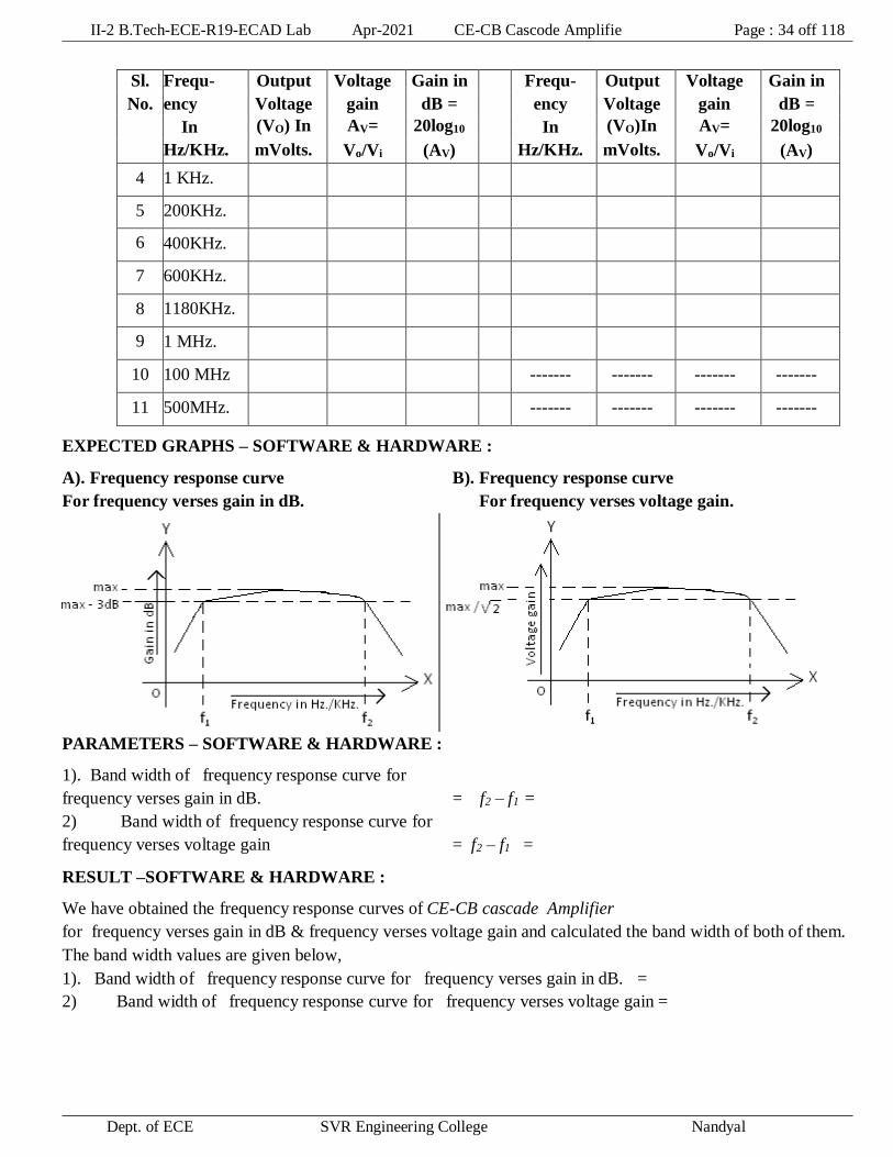
TABULAR COLUMNS :
Input Voltage (Vi) = 20 mVP-P (0.02V) is constant for all readings.
For Software : For Hardware :
Sl. Frequ- Output Voltage Gain in Frequ- Output Voltage Gain in
No. ency Voltage gain dB = ency Voltage gain dB =
In (VO) In AV= 20log10 In (VO)In AV= 20log10
Hz/KHz. mVolts. Vo/Vi (AV) Hz/KHz. mVolts. Vo/Vi (AV)
1 20 Hz.
2 100 Hz.
3 200 Hz.
----------------- To be continued in next page ---------------
II-2 B.Tech-ECE-R19-ECAD Lab Apr-2021 CE-CB Cascode Amplifie Page : 34 off 118
Dept. of ECE SVR Engineering College Nandyal
Sl. Frequ- Output Voltage Gain in Frequ- Output Voltage Gain in
No. ency Voltage gain dB = ency Voltage gain dB =
In (VO) In AV= 20log10 In (VO)In AV= 20log10
Hz/KHz. mVolts. Vo/Vi (AV) Hz/KHz. mVolts. Vo/Vi (AV)
4 1 KHz.
5 200KHz.
6 400KHz.
7 600KHz.
8 1180KHz.
9 1 MHz.
10 100 MHz ------- ------- ------- -------
11 500MHz. ------- ------- ------- -------
EXPECTED GRAPHS – SOFTWARE & HARDWARE :
A). Frequency response curve B). Frequency response curve
For frequency verses gain in dB. For frequency verses voltage gain.
PARAMETERS – SOFTWARE & HARDWARE :
1). Band width of frequency response curve for
frequency verses gain in dB. = f2 – f1 =
2) Band width of frequency response curve for
frequency verses voltage gain = f2 – f1 =
RESULT –SOFTWARE & HARDWARE :
We have obtained the frequency response curves of CE-CB cascade Amplifier
for frequency verses gain in dB & frequency verses voltage gain and calculated the band width of both of them.
The band width values are given below,
1). Band width of frequency response curve for frequency verses gain in dB. =
2) Band width of frequency response curve for frequency verses voltage gain =

II-2 B.Tech-ECE-R19-ECAD Lab Apr-2021 CE-CB Cascode Amplifie Page : 35 off 118
Dept. of ECE SVR Engineering College Nandyal
1. What is cascode Amplifier?
2. CE-CB configuration is having which Amplifier?
3. Applications of Multi stage amplifiers?
4. Mention Advantages of Multistage Amplifiers
5. What is Band Width?
6. What is Frequency Response?
7. What is cascade Amplifier?
8. Explain the transistor operation with the help of four regions
9. Explain base width modulation of a transistor
10. Compare CB,CE, CC configurations of a transistor.

II-2 B.Tech-ECE-R19-ECAD Lab Apr-2021 Voltg. Ser. F/B Amplifier Page : 37 off 118
Dept. of ECE SVR Engineering College Nandyal
AIM :
To design and obtain the frequency response of Voltage series feedback using software and
hardware.
APPARATUS :
Software :
1. System 1 No.
2. Multisim software
Hardware : 1). Function generator(FG)
2). Cathode Ray Oscilloscope(CRO)
3). Regulated Power Supply (RPS) :
4). Probes
(0-30)V, 1A
Dual channel
-------- 1 No.
-------- 1 No.
-------- 1 No.
-------- 1 No.
5). Bread board
6). Connecting wires :
1). Transisitor a). BC547 NPN
2). Resistors a). 47K Ω
b). 10 K Ω
d). 1 K Ω
3). Capacitors a). 0.22 µF
-------- 1 No.
-------- A few Nos.
---------1 No.
-------- 1 No.
-------- 1 No.
-------- 1 No.
-------- 2 No.
THEORY :
Feedback :
Feedback is said to exist in an amplifier circuit, when a fraction of the output signal is returned or fed
back to the input and combined with the input signal. If the magnitude of the input signal is reduced by the feed
back, the feed back is called negative or degenerative. If the magnitude of the input signal is increased by the
feed back, such feed back is called positive or regenerative.
Definition :
When any increase in the output signal results into the input in such a way as to cause the decrease in the
output signal, the amplifier is said to have negative feedback. ... In Voltage-Series feedback, the input
impedance of the amplifier is increased and the output impedance is decreased.
True voltage :
Voltage series feedback amplifier have the difference voltage, Vid = Vin-Vf. Therefore, the
feedback voltage always opposes the input voltage and is out of phase by 180o with respect to input voltage.
Hence, the feedback is said to be negative.
Benefit of hifgh input impedance :
1. It provides good amplification to the input signal otherwise we get low voltage and that leads to low
amplification
2. It minimizing the loading effectr on input and thus significant amount of input voltage signal is maintained
for amplification.
Experiment No. : 6 Date :
Name of the Experiment : VOLTAGE SERIES FEEDBACK AMPLIFIER

II-2 B.Tech-ECE-R19-ECAD Lab Apr-2021 Voltg. Ser. F/B Amplifier Page : 38 off 118
Dept. of ECE SVR Engineering College Nandyal
CIRCUIT DIAGRAM – SOFTWARE & HARDWARE :
PROCEDURE – SOFTWARE :
1. We have picked up the components from the components bar as per above circuit.
2. Made the connections as per the above circuit diagram by using the components which we have
picked up.
3. Connected the CRO across the Emitter capacitor to ground..
4. Set the input signal as sine wave form 20mVP-P and 1KHz. as constant in the function generator.
5. To simulate the circuit clicked on run option through execute button in tool bar.
6. We have seen the sine wave on the CRO screen as o/p signal.
7. Calculated the peak to peak voltage (VO(p-p)) and noted down in the tabular form against the
column of 1KHz.
8. Stopped the simulation by clicked on run option through execute button in the tool bar.
9. Repeated the same procedure from points 5 to 8 for the corresponding frequency values by setting
in the function generator for the following steps,
20Hz, 100Hz., 200Hz., 500Hz, 1KHz, 200KHz, 400KHz,600KHz, 1180KHz, 1MHz, 100MHz,
500MHz. in
the function generator.
10. Observed the graph for frequency Vs amplitude through the AC Analysis.
11. Finally shut down the system safely.
12. We have observed that, the graph which is drawn by manually is same to the graph which is obtained
from the AC Analysis.

II-2 B.Tech-ECE-R19-ECAD Lab Apr-2021 Voltg. Ser. F/B Amplifier Page : 39 off 118
Dept. of ECE SVR Engineering College Nandyal
13. Now calculated and noted down the values of voltage gain(AV) and gain in dB to the corresponding
values of output voltage(VO) & input voltage(Vi) by using the formulas given below,
Voltage gain (Av) = Vo / Vi and Gain in dB = 20log10(Av).
PROCEDURE – HARDWARE :
1). Connected the circuit as per the circuit diagram.
2). Removed the probe of CRO from output (O/P) side and connected it at input (I/P) side to set the input
signal
i.e. sine wave having the value of 20mVp-p&1KHz.
3). Then switched ON the function generator and CRO; but don’t switched ON the
RPS. 4). Now Kept the AC/GND/DC switch is at AC position.
5). Now applied the input signal i.e. sine wave by pressing the sine wave function key in the
function generator.
6). Initially kept the peak to peak amplitude of a sine wave is of 20mVp-p , 1KHz. frequency by
varying the amplitude and frequency controls in he function generator through observing in the
CRO.
7). Kept this value of input signal as constant up to the completion of the experiment Otherwise the
wrong output would occurred.
8) Then removed the probe of CRO from the input side and connected it across the output
side. 9). Now switched ON the RPS and set the 10V in it i.e. VCC = 12V.
10). Varied the different frequency steps of 20Hz, 100Hz., 200Hz., 500Hz, 1KHz, 100KHz, 200KHz,
400KHz, 600KHz, 1180KHz,1MHz. by adjusted the frequency control in the function generator and
noted down the corresponding values of output signal i.e. peak to peak amplitude (voltage) of sine
wave by observing in the CRO.
11). Now switched OFF the RPS, function generator and CRO.
12). Then calculated the voltage gain AV = VO/Vi & gain in dB = 20log10(AV) and noted down the values
in the specified columns of the tabular column.
Notes:
1. Amplifier means which amplifies the sinusoidal and non-sinusoidal wave forms with out
change in frequency. In voltage series feedback amplifier, network is in parallel with the the
output of the amplifier.
2. A fraction of the output voltage through the feedback network is applied in series with in the
input voltage of the amplifier.
3. The series connections at the input, increase the input resistance. In this case the
amplifier is a true voltage amplifier.
4. The common collector or emitter follower is an example of voltage series feedback amplifier.
Since the voltage developed in the output is in series with the input voltage as for as the base –
emitter junction is connected.

II-2 B.Tech-ECE-R19-ECAD Lab Apr-2021 Voltg. Ser. F/B Amplifier Page : 40 off 118
Dept. of ECE SVR Engineering College Nandyal
TABULAR COLUMN :
Input Voltage (Vi) = 20 mVP-P (0.02V) is constant for all readings.
For Software : For Hardware :
Sl.No. Frequ- Output Voltage Gain in Frequ- Output Voltag Gain in
ency Voltage gain dB = ency Voltage e dB =
In (VO) In AV= 20log10 In (VO)In gain 20log10
Hz/KHz. mVolts. Vo/Vi (AV) Hz/KHz. mVolts. AV= (AV)
Vo/Vi
1 20 Hz.
2 100 Hz.
3 200 Hz.
4 1 KHz.
5 200KHz.
6 400KHz.
7 600KHz.
8 1180KHz.
9 1 MHz.
10 100 MHz ------- ------- ------- -------
11 500MHz. ------- ------- ------- -------
EXPECTED GRAPH – SOFTWARE & HARDWARE :
Note : We could not drawn frequency response curve and not to be calculate band width for this
experiment, because there is no any amplification. It is just working as buffer.
RESULT – SOFTWARE & HARDWARE :
We have obtained the Voltage gain & Gain in db of a given amplifier.

II-2 B.Tech-ECE-R19-ECAD Lab Apr-2021 Voltg. Ser. F/B Amplifier Page : 41 off 118
Dept. of ECE SVR Engineering College Nandyal
VIVA VOICE QUESTIONS:
1. What is feedback?
2. What are the advantages of negative feedback?
3. What are the feedback topologies?
4. Example for voltage series feedback amplifier.
5. What are the CC Amplifier characteristics?
6. What are the Applications of Multi stage amplifiers?
7. Example for voltage series feedback amplifier.
8. CC Amplifier characteristics?
9. What is Band Width?
10. Explain the transistor operation with the help of four regions

II-2 B.Tech-ECE-R19-ECAD Lab Apr-2021 Current Shnt F/B Amplifier Page : 43 off 118
Dept. of ECE SVR Engineering College Nandyal
AIM :
1). To plot the graph for frequency response curve of a Current shunt feedback Amplifier with feed back and
without feedback using software and hardware
2). To find the bandwidth of Current shunt feedback Amplifier.
APPARATUS :
Software :
1. System 1 No.
2. Multisim software
Hardware :
1). Function generator(FG)
2). Cathode Ray
Oscilloscope(CRO) 3).
Regulated Power Supply (RPS)
: 4). Probes
(0-30)V, 1A
Dual channel
-------- 1 No.
-------- 1 No.
-------- 1 No.
-------- 1 No.
5). Bread board
6). Connecting wires :
-------- 1 No.
-------- A few Nos.
COMPONENTS :
1). Transistor BC 547 --------- 2 No.
2) Carbon fixed resistors a). 47KΩ, 10KΩ , 4.7 KΩ , 1 KΩ , ½W -------- Each 2 2 No.
b). 100 Ω , ½W -------- 1 No.
3). Capacitors a). 0.22µF -------- 4 No.
b). 10µF -------- 1 No.
c). 33µF -------- 1 No.
THEORY :
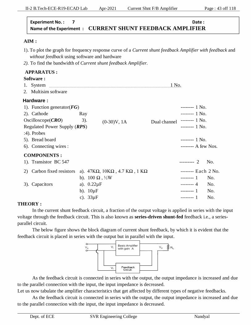
In the current shunt feedback circuit, a fraction of the output voltage is applied in series with the input
voltage through the feedback circuit. This is also known as series-driven shunt-fed feedback i.e., a series-
parallel circuit.
The below figure shows the block diagram of current shunt feedback, by which it is evident that the
feedback circuit is placed in series with the output but in parallel with the input.
As the feedback circuit is connected in series with the output, the output impedance is increased and due
to the parallel connection with the input, the input impedance is decreased.
Let us now tabulate the amplifier characteristics that get affected by different types of negative feedbacks.
As the feedback circuit is connected in series with the output, the output impedance is increased and due
to the parallel connection with the input, the input impedance is decreased.
Experiment No. : 7 Date :
Name of the Experiment : CURRENT SHUNT FEEDBACK AMPLIFIER
II-2 B.Tech-ECE-R19-ECAD Lab Apr-2021 Current Shnt F/B Amplifier Page : 44 off 118
Dept. of ECE SVR Engineering College Nandyal
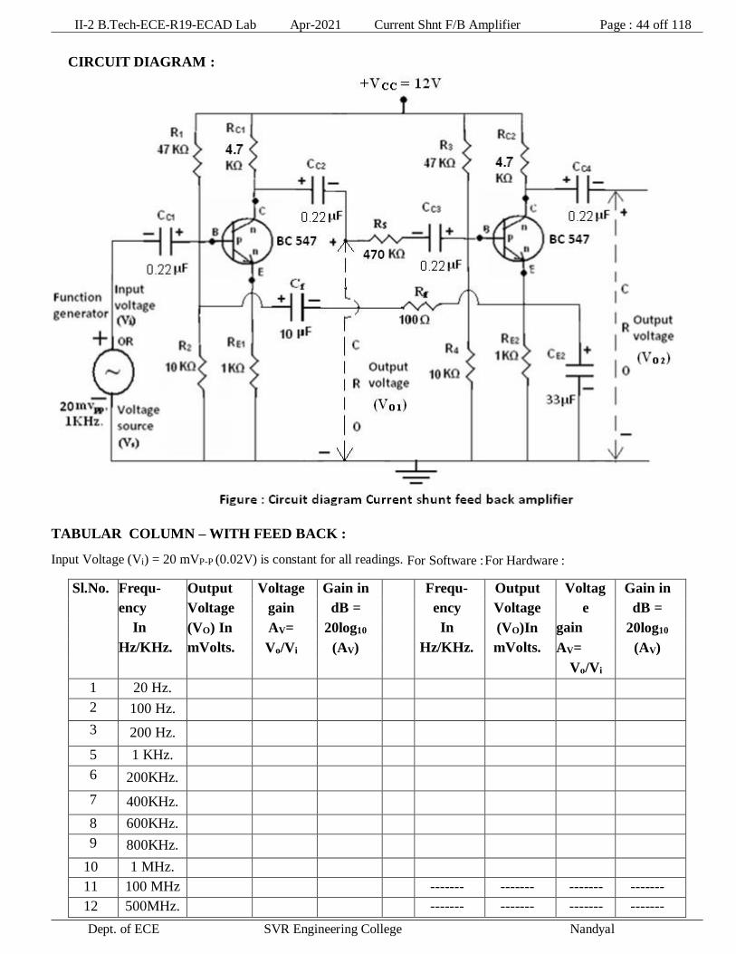
CIRCUIT DIAGRAM :
TABULAR COLUMN – WITH FEED BACK :
Input Voltage (Vi) = 20 mVP-P (0.02V) is constant for all readings. For Software : For Hardware :
Sl.No. Frequ- Output Voltage Gain in Frequ- Output Voltag Gain in
ency Voltage gain dB = ency Voltage e dB =
In (VO) In AV= 20log10 In (VO)In gain 20log10
Hz/KHz. mVolts. Vo/Vi (AV) Hz/KHz. mVolts. AV= (AV)
Vo/Vi
1 20 Hz.
2 100 Hz.
3 200 Hz.
5 1 KHz.
6 200KHz.
7 400KHz.
8 600KHz.
9 800KHz.
10 1 MHz.
11 100 MHz ------- ------- ------- -------
12 500MHz. ------- ------- ------- -------

II-2 B.Tech-ECE-R19-ECAD Lab Apr-2021 Current Shnt F/B Amplifier Page : 45 off 118
Dept. of ECE SVR Engineering College Nandyal
TABULAR COLUMN – WITHOUT FEED BACK :
Input Voltage (Vi) = 20 mVP-P (0.02V) is constant for all readings.
For Software : For Hardware :
Sl.No. Frequ- Output Voltage Gain in Frequ- Output Voltag Gain in
ency Voltage gain dB = ency Voltage e dB =
In (VO) In AV= 20log10 In (VO)In gain 20log10
Hz/KHz. mVolts. Vo/Vi (AV) Hz/KHz. mVolts. AV= (AV)
Vo/Vi
1 20 Hz.
2 100 Hz.
3 200 Hz.
4 1 KHz.
5 200KHz.
6 400KHz.
7 600KHz.
8 1180KHz.
9 1 MHz.
10 100 MHz ------- ------- ------- -------
11 500MHz. ------- ------- ------- -------
PROCEDURE – SOFTWARE :
1. We have picked up the components from the components bar as per above circuit.
2. Made the connections as per the above circuit diagram by using the components which we have
picked up.
3. Connected the CRO across the capacitor CC4.
4. Set the input signal as sine wave form which is having the value 20mVP-P as constant in the
function generator.
5. Initially set the input signal frequency value is 1KHz in the function generator.
6. To simulate the circuit clicked on run option through execute button in tool bar.
7. We have seen the sine wave on the CRO screen as o/p signal.
8. Calculated the peak to peak voltage (VO(p-p)) and noted down in the column of 1 KHz. in tabular form of
with feedback amplifier.
9. Stopped the simulation by clicked on run option through execute button in the tool bar.
10. Repeat the same procedure from points 6 to 9 for the corresponding frequency values by setting
in the function generator for the following steps, 20Hz, 100Hz., 200Hz., 1KHz, 200KHz,
400KHz, 600KHz, 1180KHz, 1MHz,100MHz, 500MHzin the function generator.
11. Observed the graph for frequency Vs amplitude through the AC Analysis.
12. Disconnected the Cf and Rf from the circuit and now the circuit has became as without feedback
amplifier

II-2 B.Tech-ECE-R19-ECAD Lab Apr-2021 Current Shnt F/B Amplifier Page : 46 off 118
Dept. of ECE SVR Engineering College Nandyal
13. Now taken the reading in the tabular form of without feedback amplifier by repeat the steps from 6 to 11
14. Finally shut down the system safely.
15. We have observed that, the graph which is drawn by manually is same to the graph which is obtained
from the AC Analysis.
16. We have observed that the readings of without feed back amplifier’s output voltage is greater than the
with feed back amplifier
17. Calculated the Voltage gain by using the formula of Vo / Vi and Gain in dB by using the formula of
20log10(AV) in both tabular forms of with feed back and without feed back amplifiers.
18. Drawn the graphs of both amplifiers in single graph sheet.
19. While drawing the graph taken the frequency on X-axis and Gain in dB on Y-axis.
20. Finally calculated the bandwidth of both amplifiers from this graph sheet as per the following
formulas, i). For Current shunt feed back amplifier (With feed back ) (BW) = f2 – f1
ii). For Current shunt feed back amplifier (Without feed back ) (BW) = f4 – f3
21. We have noted down that the band width of with feed back amplifier is high compared to the
without feed back amplifier.
PROCEDURE – HARDWARE :
1. Connections are made as per the circuit diagram.
2. Initially connected the CRO across the Function generator.
3. Switched ON the Cathode ray oscilloscope (CRO) and Function generator.
4. Applied the 20 mVpp , 1Khz sine wave signal to the circuit from Function generator by observing in
the
CRO.
5. We have kept this 20 mVpp input voltage as constant for all steps of frequency while
taking the readings for Current shunt feed back amplifier with feed back & without feed back .
6. Disconnected the CRO from the function generator, and connected it across CC4 to measure the
peak to peak output voltage.
7. Now Connected the CRO at output side
8. Applied the +VCC as 10V to the circuit from the Regulated power supply (RPS).
9. Later we have noted down the readings for output voltage in the tabular form of with feed back.
from the CRO, by varying the different steps of frequency (i.e. 20Hz, 100Hz., 200Hz., 500Hz.,
1KHz, 200KHz, 400KHz, 600KHz, 1180KHz, 1MHz.) in function generator.
10. After this we removed the feed back capacitor (Cf ) & resistor (Rf) from the circuit completely then
the circuit is became as the without feed back amplifier.
11. Again we have noted down the readings for output voltage in the tabular form of without feed
back from the CRO, by varying the different steps of frequency (i.e. 10Hz, 500Hz, 1KHz, 100KHz,
200KHz, 400KHz, 600KHz, 1180KHz, 1MHz.) in function generator.
12. We have observed that the readings of without feed back amplifier’s
output voltage is greater than the with feed back amplifier.
13. Finally we switched OFF the function generator, cathode ray oscilloscope and regulated power
supply.
14. Calculated the Voltage gain by using the formula of Vo / Vi and Gain in dB by
using the formula of 20log10(AV) in both tabular forms of with feed back and without feed back
amplifiers.
15. Drawn the graphs of both amplifiers in single graph sheet.

II-2 B.Tech-ECE-R19-ECAD Lab Apr-2021 Current Shnt F/B Amplifier Page : 47 off 118
Dept. of ECE SVR Engineering College Nandyal
16. While drawing the graph taken the frequency on X-axis and Gain in dB on Y-axis.
17. Finally calculated the bandwidth of both amplifiers from this graph sheet as per the following
formulas, i). For Current shunt feed back amplifier (With feed back ) (BW) = f2 – f1
ii). For Current shunt feed back amplifier (Without feed back ) (BW) = f4 – f3
18.We have noted down that the band width of with feed back amplifier is high as compared to the
without feed back amplifier.
EXPECTED GRAPH – SOFTWARE & HARDWARE :
The following graph shows for Current shunt feed back amplifier with feed back and
without Feedback amplifier for software as well as hardware.
RESULT – SOFTWARE & HARDWARE :
We drawn the graph for frequency response of a Current shunt feedback amplifier for both
with feedback and without feedback.
II-2 B.Tech-ECE-R19-ECAD Lab Apr-2021 Current Shnt F/B Amplifier Page : 48 off 118
Dept. of ECE SVR Engineering College Nandyal
VIVA VOICE QUESTIONS:
1. What is feedback?
2. What are the input and output impedances for current shunt feedback Amplifier.
3. Applications of current shunt feedback Amplifier.
4. Mention Applications of single Tuned Amplifier.
5. What are the feedback topologies?
6. Example for voltage series feedback amplifier.
7. CC Amplifier characteristics?
8. What is Band Width?
9. What is Frequency Response?
10. Explain the transistor operation with the help of four regions

II-2 B.Tech-ECE-R19-ECAD Lab Apr-2021 Single Tuned Voltg. Amplifier Page : 49 off 118
Dept. of ECE SVR Engineering College Nandyal
AIM :
To obtain the frequency response curve of Single tuned voltage amplifier using software and Hard
ware
APPARATUS :
1. System with Multisim software ------------------------------ 1 No.
2. Regulated power supply ( RPS ) ------------------------------ 1 No.
3. Cathode Ray Oscilloscope ( CRO) ------------------------------ 1 No.
4. Function generator 1 No.
5. Decade Inductance box (DIB) ------------------------------------- 1 No.
6. Decade capacitance box (DCB) ------------------------------------ 1 No.
7. Probes ---------------------------------- 1 No.
8. Breadboard ---------------------------------- 1 No.
9. Connecting wires ---------------------------------- 1 No.
COMPONENTS :
1. Transistor BC 547 ------------------------------ 1 No.
2. Resistors 47KΩ, 10KΩ, 1 KΩ, ------------ Each 1No.
3. Capacitors 0.22µF, ------------ 2 No.
33 µF ------------ 1 No.
4. Resistors 47KΩ, 10 KΩ, 1KΩ ------------ Each 1 No.
THEORY :
Tuned amplifiers are mainly preferred to amplify the high-frequency signals in wireless communication.
The tuned amplification works based on the tuning circuit implied as load. The range of the frequencies defined
for a particular amplification circuit can be fixed or dynamic based on applications. The tuning circuit present at
the load consists of an inductor and capacitor. For dynamic frequencies, the values of capacitance should be
varied. These amplifiers are very advantageous due to its appealing large bandwidths. The increment in
bandwidth is based on the number of tuning circuits present at the load. There are three types of most frequently
used tuned amplifiers they are single tuned amplifier, double-tuned amplifier and stagger tuned amplifier.
Definition: A tuned amplifier consists of a single tuning circuit at the load can be defined as a single
tuned amplifier. It is a multi-stage amplifier, where each stage of this amplifier must be tuned with the same
frequencies. For example, tuning a radio station. If the desired carrier wave is passed and matches the defined
range of passband frequency, then the radio station is tuned otherwise it is blocked.
Experiment No. : 8 Date :
Name of the Experiment : SINGLE TUNED VOLTAGE AMPLIFIER

II-2 B.Tech-ECE-R19-ECAD Lab Apr-2021 Single Tuned Voltg. Amplifier Page : 50 off 118
Dept. of ECE SVR Engineering College Nandyal
CIRCUIT DIAGRAM – SOFTWARE & HARDWARE :
THEORETICAL CALCULATIONS – SOFTWARE & HARDWARE :
PROCEDURE – SOFTWARE :
1. We have picked up the components from the components bar as per above circuit.
2. Made the connections as per the above circuit diagram by using the components which we have
picked up.
3. Connected the CRO across the Collector capacitor to ground..
4. Kept the L=4.7mH to take readings in tabular form-1
5. Set the input signal as sine wave form at 20mVP-P, 10KHz. as constant in the function Generator
until the experiment would completed.
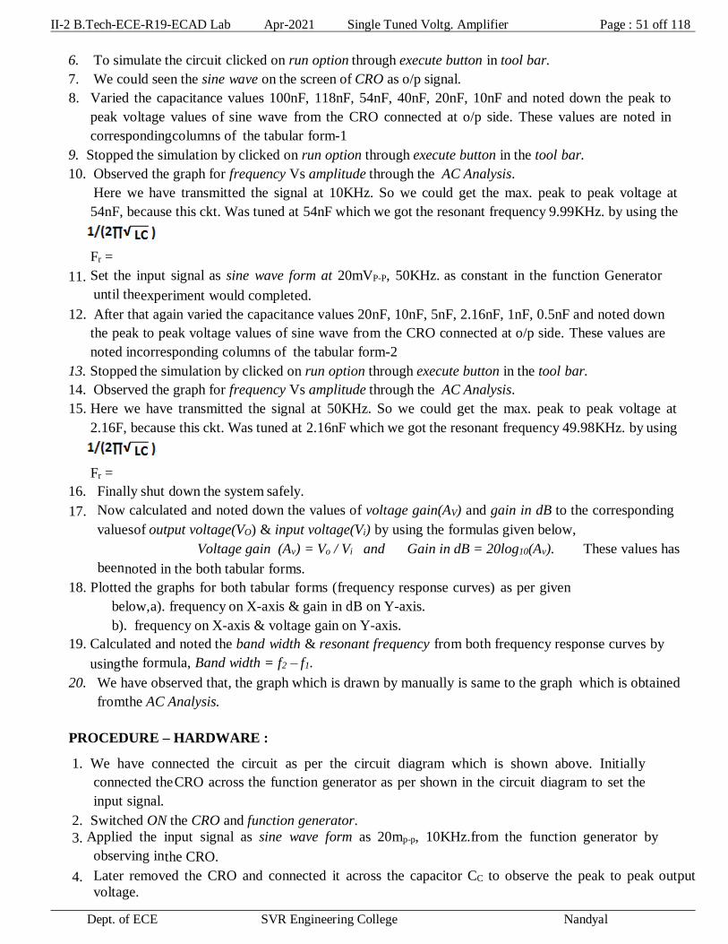
II-2 B.Tech-ECE-R19-ECAD Lab Apr-2021 Single Tuned Voltg. Amplifier Page : 51 off 118
Dept. of ECE SVR Engineering College Nandyal
6. To simulate the circuit clicked on run option through execute button in tool bar.
7. We could seen the sine wave on the screen of CRO as o/p signal.
8. Varied the capacitance values 100nF, 118nF, 54nF, 40nF, 20nF, 10nF and noted down the peak to
peak voltage values of sine wave from the CRO connected at o/p side. These values are noted in
corresponding columns of the tabular form-1
9. Stopped the simulation by clicked on run option through execute button in the tool bar.
10. Observed the graph for frequency Vs amplitude through the AC Analysis.
Here we have transmitted the signal at 10KHz. So we could get the max. peak to peak voltage at
54nF, because this ckt. Was tuned at 54nF which we got the resonant frequency 9.99KHz. by using the
formula
Fr =
11. Set the input signal as sine wave form at 20mVP-P, 50KHz. as constant in the function Generator
until the experiment would completed.
12. After that again varied the capacitance values 20nF, 10nF, 5nF, 2.16nF, 1nF, 0.5nF and noted down
the peak to peak voltage values of sine wave from the CRO connected at o/p side. These values are
noted in corresponding columns of the tabular form-2
13. Stopped the simulation by clicked on run option through execute button in the tool bar.
14. Observed the graph for frequency Vs amplitude through the AC Analysis.
15. Here we have transmitted the signal at 50KHz. So we could get the max. peak to peak voltage at
2.16F, because this ckt. Was tuned at 2.16nF which we got the resonant frequency 49.98KHz. by using
the formula
Fr =
16. Finally shut down the system safely.
17. Now calculated and noted down the values of voltage gain(AV) and gain in dB to the corresponding
values of output voltage(VO) & input voltage(Vi) by using the formulas given below,
Voltage gain (Av) = Vo / Vi and Gain in dB = 20log10(Av). These values has
been noted in the both tabular forms.
18. Plotted the graphs for both tabular forms (frequency response curves) as per given
below, a). frequency on X-axis & gain in dB on Y-axis.
b). frequency on X-axis & voltage gain on Y-axis.
19. Calculated and noted the band width & resonant frequency from both frequency response curves by
using the formula, Band width = f2 – f1.
20. We have observed that, the graph which is drawn by manually is same to the graph which is obtained
from the AC Analysis.
PROCEDURE – HARDWARE :
1. We have connected the circuit as per the circuit diagram which is shown above. Initially
connected the CRO across the function generator as per shown in the circuit diagram to set the
input signal.
2. Switched ON the CRO and function generator.
3. Applied the input signal as sine wave form as 20mp-p, 10KHz.from the function generator by
observing in the CRO.
4. Later removed the CRO and connected it across the capacitor CC to observe the peak to peak output
voltage.

II-2 B.Tech-ECE-R19-ECAD Lab Apr-2021 Single Tuned Voltg. Amplifier Page : 52 off 118
Dept. of ECE SVR Engineering College Nandyal
5. Kept the L=4.7mH in the DIB.
6. Switched ON the RPS and kept the 12V as VCC.
7. Now Noted down the peak to peak voltage of o/p signal by varied capacitance values- 100nF, 118nF,
54nF, 40nF, 20nF, 10nF from the DCB in the corresponding column of the tabular form-3
8. If we observed, for C=54nF only we got max. peak to peak voltage, because this ckt. Was
tuned at frequency of 10KHz.
9. Again, Applied the input signal as sine wave form as 20mp-p, 50KHz.from the function
generator by observing in the CRO, and L=4.7mH.
10. Now Noted down the peak to peak voltage of o/p signal by varied capacitance values- 20nF, 10nF,
5nF, 2.16nF, 1nF, 0.5nF from the DCB. In corresponding column of the tabular form-4
11. If we observed, for C=2.16nF only we got max. peak to peak voltage, because this ckt. Was tuned
at frequency of 50KHz.
12. Now calculated and noted down the values of voltage gain(AV) and gain in dB to the
corresponding values of output voltage(VO) & input voltage(Vi) by using the formulas given
below,
i. Voltage gain (Av) = Vo / Vi and Gain in dB = 20log10(Av). These values has been
noted in the both tabular forms-3 & 4.
13. Plotted the graphs for both tabular forms – 3&4 (frequency response curves) as per given
below, a). frequency on X-axis & gain in dB on Y-axis.
a. b). frequency on X-axis & voltage gain on Y-axis.
14. Calculated and noted the band width & resonant frequency from both frequency response
curves by using the formula, Band width = f2 – f1.
TABULAR FORM – 1 – SOFTWARE :
Input voltage (Vi) = 20mVp-p (0.02v) is constant for all readings.
When fr = 10Khz. , C = 54 nF, L = 4.7mH,
Sl.
No.
Induct-
ance (L)
In mH
Capacit-
Ance (C)
In nF
Capacitance
Setting in %
Resonant
Frequency
in KHz.
Output
Voltage
(VO)
In Volts.
Volt-age
gain
AV =
Vo/Vi
Gain in
dB =
20log10
(AV)
1 4.7 100 100 7.34
2 4.7 118 118 8.21
3 4.7 54 54 9.99
4 4.7 40 40 11.61
5 4.7 20 20 16.42
6 4.7 10 10 23.22
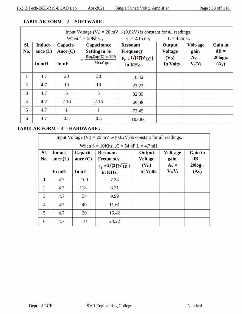
II-2 B.Tech-ECE-R19-ECAD Lab Apr-2021 Single Tuned Voltg. Amplifier Page : 53 off 118
Dept. of ECE SVR Engineering College Nandyal
TABULAR FORM – 2 – SOFTWARE :
Input Voltage (Vi) = 20 mVP-P (0.02V) is constant for all readings.
When fr = 50Khz. , C = 2.16 nF, L = 4.7mH,
Sl.
No.
Induct-
ance (L)
In mH
Capacit-
Ance (C)
In nF
Capacitance
Setting in %
Resonant
Frequency
in KHz.
Output
Voltage
(VO)
In Volts.
Volt-age
gain
AV =
Vo/Vi
Gain in
dB =
20log10
(AV)
1 4.7 20 20 16.42
2 4.7 10 10 23.23
3 4.7 5 5 32.85
4 4.7 2.16 2.16 49.98
5 4.7 1 1 73.45
6 4.7 0.5 0.5 103.87
TABULAR FORM – 3 – HARDWARE :
Input Voltage (Vi) = 20 mVP-P (0.02V) is constant for all readings.
When fr = 10Khz. ,C = 54 nF,L = 4.7mH,
Sl.
No.
Induct-
ance (L)
In mH
Capacit-
ance (C)
In nF
Resonant
Frequency
in KHz.
Output
Voltage
(VO)
In Volts.
Volt-age
gain
AV =
Vo/Vi
Gain in
dB =
20log10
(AV)
1 4.7 100 7.34
2 4.7 118 8.21
3 4.7 54 9.99
4 4.7 40 11.61
5 4.7 20 16.42
6 4.7 10 23.22
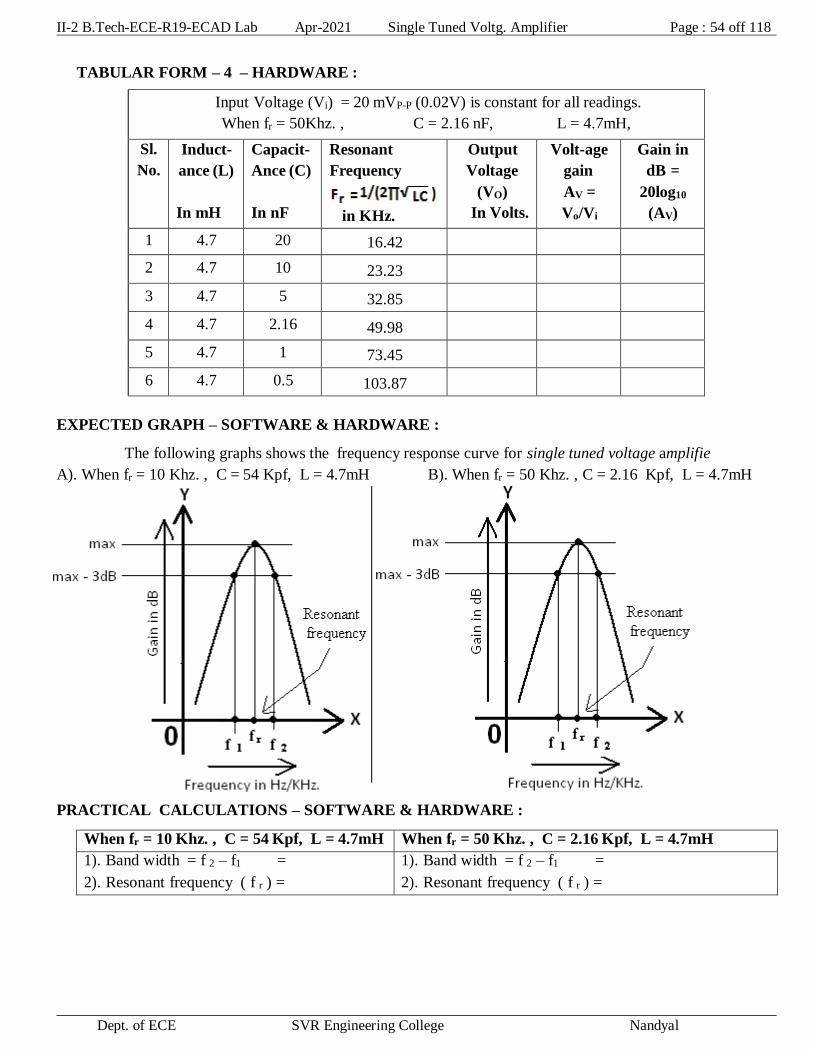
II-2 B.Tech-ECE-R19-ECAD Lab Apr-2021 Single Tuned Voltg. Amplifier Page : 54 off 118
Dept. of ECE SVR Engineering College Nandyal
TABULAR FORM – 4 – HARDWARE :
Input Voltage (Vi) = 20 mVP-P (0.02V) is constant for all readings.
When fr = 50Khz. , C = 2.16 nF, L = 4.7mH,
Sl.
No.
Induct-
ance (L)
In mH
Capacit-
Ance (C)
In nF
Resonant
Frequency
in KHz.
Output
Voltage
(VO)
In Volts.
Volt-age
gain
AV =
Vo/Vi
Gain in
dB =
20log10
(AV)
1 4.7 20 16.42
2 4.7 10 23.23
3 4.7 5 32.85
4 4.7 2.16 49.98
5 4.7 1 73.45
6 4.7 0.5 103.87
EXPECTED GRAPH – SOFTWARE & HARDWARE :
The following graphs shows the frequency response curve for single tuned voltage amplifie
A). When fr = 10 Khz. , C = 54 Kpf, L = 4.7mH B). When fr = 50 Khz. , C = 2.16 Kpf, L = 4.7mH
PRACTICAL CALCULATIONS – SOFTWARE & HARDWARE :
When fr = 10 Khz. , C = 54 Kpf, L = 4.7mH When fr = 50 Khz. , C = 2.16 Kpf, L = 4.7mH
1). Band width = f 2 – f1 =
2). Resonant frequency ( f r ) =
1). Band width = f 2 – f1 =
2). Resonant frequency ( f r ) =
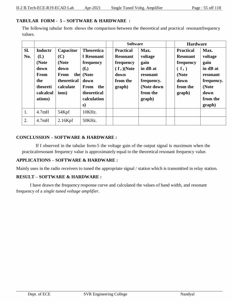
II-2 B.Tech-ECE-R19-ECAD Lab Apr-2021 Single Tuned Voltg. Amplifier Page : 55 off 118
Dept. of ECE SVR Engineering College Nandyal
TABULAR FORM - 5 – SOFTWARE & HARDWARE :
The following tabular form shows the comparison between the theoretical and practical resonant frequency
values.
Software Hardware
Sl.
No.
Inductr
(L)
(Note
down
From
the
theoreti
calcalcul
ations)
Capacitor
(C)
(Note
down
From the
theoretical
calculate
ions)
Theoretica
l Resonant
frequency
(fr)
(Note
down
From the
theoretical
calculation
s)
Practical
Resonant
frequency
( f r )(Note
down
from the
graph)
Max.
voltage
gain
in dB at
resonant
frequency.
(Note down
from the
graph)
Practical
Resonant
frequency
( f r )
(Note
down
from the
graph)
Max.
voltage
gain
in dB at
resonant
frequency.
(Note
down
from the
graph)
1. 4.7mH 54Kpf 10KHz.
2. 4.7mH 2.16Kpf 50KHz.
CONCLUSSION – SOFTWARE & HARDWARE :
If I observed in the tabular form-5 the voltage gain of the output signal is maximum when the
practical resonant frequency value is approximately equal to the theoretical resonant frequency value.
APPLICATIONS – SOFTWARE & HARDWARE :
Mainly uses in the radio receivers to tuned the appropriate signal / station which is transmitted in relay station.
RESULT – SOFTWARE & HARDWARE :
I have drawn the frequency response curve and calculated the values of band width, and resonant
frequency of a single tuned voltage amplifier.
II-2 B.Tech-ECE-R19-ECAD Lab Apr-2021 Single Tuned Voltg. Amplifier Page : 56 off 118
Dept. of ECE SVR Engineering College Nandyal
VIVA VOICE Questions:
1. What is single Tuned Amplifier?
2. What is Q factor?
3. What is tank circuit?
4. Mention Applications of single Tuned Amplifier.
5. What is the resonant frequency of single tuned Amplifier?
6. Tuned Amplifier is Narrow or Wide BW Amplifier?
7. Difference between single tuned and double tuned Amplifier?
8. What is stagger tuned Amplifier?
9. Effect of cascading of single tuned Amplifier on BW?
10. What is frequency response?

II-2 B.Tech-ECE-R19-ECAD Lab Apr-2021 Class A Power Amplifier Page : 57 off 118
Dept. of ECE SVR Engineering College Nandyal
AIM :
1. To verify / plot the output signal (sine wave form) of a given Class-A Series-fed Power Aamplifier by
using software & hardware .
2. To calculate the conversion efficiency of a given amplifier.
APPARATUS :
1. System with Multisim software --------------- 1 No.
2. Regulated Power Supply (0-30)V, 1A ------------ 1 No.
3. Function generator 1MHz. --------------- 1 No.
4. Probes ------- --------------- 1 No.
5. Bread board ------- --------------- 1 No.
6. Connecting wires ------- --------------- A few Nos.
7. Ammeters (0-10)mA DC Type 1 No.
COMPONENTS :
1. Transistors BC 547 --------------- 1 No.
2. Resistors 1KΩ, 10 KΩ, 47 KΩ Each 1 No.
3. Capacitors 0.22µF --------------- 2 No.
33 µF --------------- 1 No.
THEORY :
Class A power amplifier is a type of power amplifier where the output transistor is ON full time and the
output current flows for the entire cycle of the input wave form. Class A power amplifier is the simplest of all
power amplifier configurations. They have high fidelity and are totally immune to crossover distortion. Even
though the class A power amplifier have a handful of good feature, they are not the prime choice because of
their poor efficiency. Since the active elements (transistors) are forward biased full time, some current will flow
through them even though there is no input signal and this is the main reason for the inefficiency
The theoretical maximum efficiency of a Class A power amplifier is 50%. In practical scenario, with
capacitive coupling and inductive loads (loud speakers), the efficiency can come down as low as 25%. This
means 75% of power drawn by the amplifier from the supply line is wasted. Majority of the power wasted is lost
as heat on the active elements (transistor).As a result, even a moderately powered Class A power amplifier
require a large power supply and a large heatsink.
Experiment No. 9 Date :
Name of the Experiment : CLASS A POWER AMPLIFIER
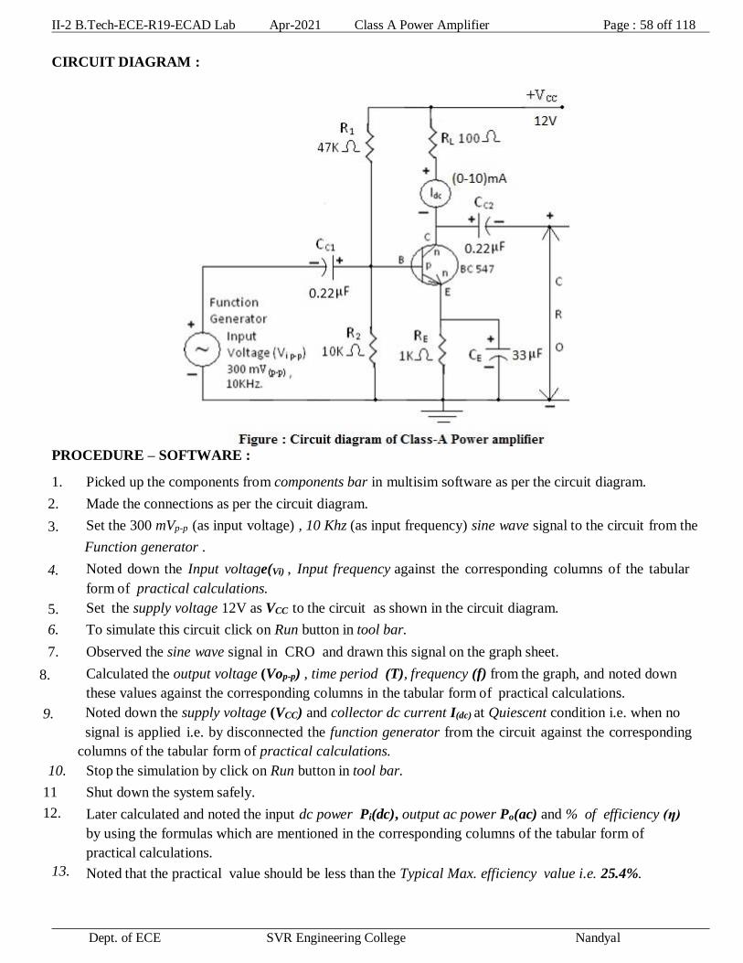
II-2 B.Tech-ECE-R19-ECAD Lab Apr-2021 Class A Power Amplifier Page : 58 off 118
Dept. of ECE SVR Engineering College Nandyal
CIRCUIT DIAGRAM :
PROCEDURE – SOFTWARE :
1. Picked up the components from components bar in multisim software as per the circuit diagram.
2. Made the connections as per the circuit diagram.
3. Set the 300 mVp-p (as input voltage) , 10 Khz (as input frequency) sine wave signal to the circuit from the
Function generator .
4. Noted down the Input voltage(Vi) , Input frequency against the corresponding columns of the tabular
form of practical calculations.
5. Set the supply voltage 12V as VCC to the circuit as shown in the circuit diagram.
6. To simulate this circuit click on Run button in tool bar.
7. Observed the sine wave signal in CRO and drawn this signal on the graph sheet.
8. Calculated the output voltage (Vop-p) , time period (T), frequency (f) from the graph, and noted down
these values against the corresponding columns in the tabular form of practical calculations.
9. Noted down the supply voltage (VCC) and collector dc current I(dc) at Quiescent condition i.e. when no
signal is applied i.e. by disconnected the function generator from the circuit against the corresponding
columns of the tabular form of practical calculations.
10. Stop the simulation by click on Run button in tool bar.
11 Shut down the system safely.
12. Later calculated and noted the input dc power Pi(dc), output ac power Po(ac) and % of efficiency (η)
by using the formulas which are mentioned in the corresponding columns of the tabular form of
practical calculations.
13. Noted that the practical value should be less than the Typical Max. efficiency value i.e. 25.4%.

II-2 B.Tech-ECE-R19-ECAD Lab Apr-2021 Class A Power Amplifier Page : 59 off 118
Dept. of ECE SVR Engineering College Nandyal
PROCEDURE – HARDWARE :
1. Connections are made as per the circuit diagram.
2. Initially connected the CRO across the Function generator.
3. Switched ON the Cathode ray oscilloscope (CRO) and Function generator.
4. Applied the 300 mVp-p , 10 Khz sine wave signal to the circuit from the Function
generator by observing on the
crt of the CRO.
5. Later connected the CRO across RL i.e at output side.
6. Now switched ON the Regulated Power Supply (RPS) and apply the supply voltage 12V as VCC
to the circuit as per shown in the figure.
7. Observed the sine wave signal on the CRT of the CRO and draw this signal on the graph sheet.
8. Now noted down the collector dc current I(dc) at Quiescent condition i.e. when no signal is applied
and supply voltage (VCC) by disconnected the function generator from the circuit against the
corresponding columns in the tabular form of practical calculations.
9. Switched OFF the function generator, RPS, CRO.
10. Noted down the Input voltage(Vi) , Input frequency against the corresponding columns in the
tabular form.
11. Calculated the output voltage (Vop-p) , time period (T), frequency (f) from the graph, and noted
down these values against the corresponding columns in the tabular form.
12. Later calculated the Input dc power Pi(dc), output ac power Po(ac) and % of efficiency (η) by
using the formulas which are mentioned in the corresponding columns in the tabular form.
13. Noted that The practical value should be less than the Typical Max. efficiency value i.e. 25.4%.
PRACTICAL CALCULATIONS – SOFTWARE & HARDWARE :
The practical calculations for the parameters are shown in the following tabular form.
Sl.No. Name of the parameter Value from
Software
Value From
Hardware
01. Input Voltage (Vi) p-p ( In mV). 300
02 Input frequency (In Khz.). 10
03 Supply DC Voltage ( VCC) (in Volts.) 10
04 Output voltage VO(p-p) (In volts.).
05 Time period (T) for output signal (In ms)
06 Fequency for output signal = 1/ T (In Khz.)
07 Collector dc current (Idc) (At quesient condition
i.e.
When no input signal is applied) (In mA.).

II-2 B.Tech-ECE-R19-ECAD Lab Apr-2021 Class A Power Amplifier Page : 60 off 118
Dept. of ECE SVR Engineering College Nandyal
Sl.No. Name of the parameter Value from
Software
Value From
Hardware
08 Collector DC current when sine wave (AC)
signal is applied as input signal ( Iac )
09 Input DC power Pi(dc) = Idc × VCC (In Watts).
10
11 % of efficiency (η) = [ PO(ac) / Pi (dc) ] ×100 =
12 Typical Max. efficiency (η) = 25.40%
EXPECTED WAVEFORM – SOFTWARE & HARDWARE :
The following waveform shows the output signal of Class A Series-fed Power Amplifier .
RESULT – SOFTWARE & HARDWARE :
I have verified / drawn the output signal and calculated the conversion efficiency of given
Class-A Series-fed Power amplifier.

II-2 B.Tech-ECE-R19-ECAD Lab Apr-2021 Class A Power Amplifier Page : 61 off 118
Dept. of ECE SVR Engineering College Nandyal
VIVA VOICE Questions:
1. What is Power Amplifier?
2. Classifications of power Amplifiers.
3. Efficiency of class A power Amplifier.
4. Difference between Direct coupled and Transformer coupled class A power Amplifier?
5. What is the amplitude (Harmonic) Distortion?
6. Where is the Q point in class A power Amplifier?
7. Applications of class A power Amplifier.
8. What are the disadvantages of class A power Amplifier.
9. Mention the conduction angle of class A power Amplifier.
10. What are the disadvantages of class A power Amplifier.

II-2 B.Tech-ECE-R19-ECAD Lab Apr-2021 Class B Power Amplr Page : 63 off 118
Dept. of ECE SVR Engineering College Nandyal
AIM :
1. To verify / plot the output signal (sine wave form) of a given Class-B Power Aamplifier by
using software & hardware .
2. To calculate the conversion efficiency of a given amplifier.
APPARATUS :
1. System with Multisim software --------------- 1 No.
2. Regulated Power Supply (0-30)V, 1A ------------ 1 No.
3. Function generator 1MHz. --------------- 1 No.
4. Probes ------- --------------- 1 No.
5. Bread board ------- --------------- 1 No.
6. Connecting wires ------- --------------- A few Nos.
7. Ammeters (0-10)mA DC Type 1 No.
COMPONENTS :
1. Transistors BC 547, Bc557--------------- Each 1 No.
2. Resistors 220KΩ, 18 KΩ Each 2 No.
1KΩ ---------------- 1 No.
10Ω ---------------- 3 No.
3. Capacitors 10µF --------------- 2 No.
THEORY :
Class B amplifier is a type of power amplifier where the active device (transistor) conducts only for one
half cycle of the input signal. That means the conduction angle is 190° for a Class B amplifier. Since the active
device is switched off for half the input cycle, the active device dissipates less power and hence the efficiency is
improved. Theoretical maximum efficiency of Class B power amplifier is 78.5%.
Class-B or Push-pull amplifiers use two “complementary” or matching transistors, one being an NPN-
type and the other being a PNP-type with both power transistors receiving the same input signal together that is
equal in magnitude, but in opposite phase to each other. This results in one transistor only amplifying one half
or 190o of the input waveform cycle while the other transistor amplifies the other half or remaining 190o of the
input waveform cycle with the resulting “two-halves” being put back together again at the output terminal.
Then the conduction angle for this type of amplifier circuit is only 190o or 50% of the input signal. This pushing
and pulling effect of the alternating half cycles by the transistors gives this type of circuit its amusing “push-
pull” name, but are more generally known as the Class B Amplifier
Experiment No. 10 Date :
Name of the Experiment : COMPLEMENTARY SYMMETRY PUSH PULL
CLASS B POWER AMPLIFIER
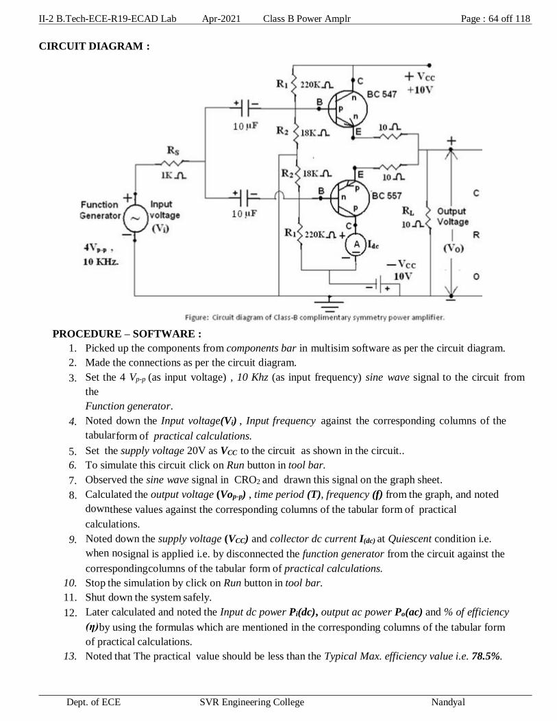
II-2 B.Tech-ECE-R19-ECAD Lab Apr-2021 Class B Power Amplr Page : 64 off 118
Dept. of ECE SVR Engineering College Nandyal
CIRCUIT DIAGRAM :
PROCEDURE – SOFTWARE :
1. Picked up the components from components bar in multisim software as per the circuit diagram.
2. Made the connections as per the circuit diagram.
3. Set the 4 Vp-p (as input voltage) , 10 Khz (as input frequency) sine wave signal to the circuit from
the
Function generator.
4. Noted down the Input voltage(Vi) , Input frequency against the corresponding columns of the
tabular form of practical calculations.
5. Set the supply voltage 20V as VCC to the circuit as shown in the circuit..
6. To simulate this circuit click on Run button in tool bar.
7. Observed the sine wave signal in CRO2 and drawn this signal on the graph sheet.
8. Calculated the output voltage (Vop-p) , time period (T), frequency (f) from the graph, and noted
down these values against the corresponding columns of the tabular form of practical
calculations.
9. Noted down the supply voltage (VCC) and collector dc current I(dc) at Quiescent condition i.e.
when no signal is applied i.e. by disconnected the function generator from the circuit against the
corresponding columns of the tabular form of practical calculations.
10. Stop the simulation by click on Run button in tool bar.
11. Shut down the system safely.
12. Later calculated and noted the Input dc power Pi(dc), output ac power Po(ac) and % of efficiency
(η) by using the formulas which are mentioned in the corresponding columns of the tabular form
of practical calculations.
13. Noted that The practical value should be less than the Typical Max. efficiency value i.e. 78.5%.

II-2 B.Tech-ECE-R19-ECAD Lab Apr-2021 Class B Power Amplr Page : 65 off 118
Dept. of ECE SVR Engineering College Nandyal
PROCEDURE – HARDWARE :
1. Connections are made as per the circuit diagram.
2. Initially connected the CRO across the Function generator.
3. Switched ON the Cathode ray oscilloscope (CRO) and Function generator.
4. Applied the 4Vp-p , 10 KHz sine wave signal to the circuit from the Function generator by
observing on the crt of the CRO.
5. Later connected the CRO across RL i.e. at output side.
6. Now switched ON the Regulated Power Supply (RPS) and apply the supply voltage +10V
from one channel (+VCC) and -10V from another (-VCC) to the circuit as per shown in the
figure.
7. Observed the sine wave signal on the CRT of the CRO and draw this signal on the graph sheet.
8. Now noted down the collector dc current I(dc) at Quiescent condition i.e. when no signal is applied
by disconnected the function generator from the circuit and supply voltage (VCC) against the
corresponding columns of the tabular form of practical calculations.
9. Noted down the Input voltage(Vi) , Input frequency against the corresponding columns of the
tabular form of practical calculations.
10. Switched OFF the function generator, RPS, CRO.
11. Calculated the peak to peak voltage (Vop-p) , peak voltage (Vm), time period (T), frequency (f)
from the graph, and noted down these values against the corresponding columns of the tabular form
of practical calculations.
12. Later calculated the Input dc power Pi(dc), output ac power Po(ac) and % of efficiency (η) by
using the formulas which are mentioned in the corresponding columns of the tabular form of
practical calculations.
13. Noted that The practical value should be less than the Typical Max. efficiency value i.e. 78.5%.
PRACTICAL CALCULATIONS – SOFTWARE & HARDWARE :
The practical calculations for the parameters are shown in the following tabular form,
Sl.
No.
Name of the parameter Value from
software
Value from
hardware
01. Input peak to peak voltage (Vi) ( In Volts). 4 4
02 Input frequency (In Khz.). 10 10
03 Positive supply DC Voltage ( +VCC) (in Volts.) 10 10
Negative supply DC Voltage ( -VCC) (in Volts.) 10 10
04 Peak to peak voltage of output VO(p-p) (In volts.).
05 Peak voltage of output (Vm) = VO(p-p) / 2 (In volts).
06 Time period (T) for output signal (In ms)
07 Fequency for output signal = 1/ T (In Khz.)
08 Collector dc current (Idc) (At quesient condition i.e.
When no input signal is applied) (In mA.).
09 Collector DC current when sine wave (AC)
signal is applied as input signal ( Iac )

II-2 B.Tech-ECE-R19-ECAD Lab Apr-2021 Class B Power Amplr Page : 66 off 118
Dept. of ECE SVR Engineering College Nandyal
Sl.
No.
Name of the parameter Value from
software
Value from
hardware
10 Input DC power Pi(dc) = Idc × VCC (In mWatts).
11
V 2
m
Output ac power Po (ac) = (In mWatts) =
2RL
12
13 Typical Max. efficiency (η) = 78.50 %
EXPECTED GRAPH - SOFTWARE & HARDWARE :
The following graph shows for Class B complementary symmetry power amplifier.
RESULT - SOFTWARE & HARDWARE :
I have drawn the graph for output signal and calculated the conversion efficiency of given
complementary symmetry Class-B push-pull power amplifier.

II-2 B.Tech-ECE-R19-ECAD Lab Apr-2021 Class B Power Amplr Page : 67 off 118
Dept. of ECE SVR Engineering College Nandyal
VIVA VOICE Questions:
1. What is Power Amplifier?
2. Classifications of power Amplifiers.
3. Efficiency of class B power Amplifier.
4. Difference between Transformer coupled and Complementary symmetry class B power Amplifier?
5. What is the Crossover Distortion?
6. Where is the Q point in class B power Amplifier?
7. Applications of class B power Amplifier.
8. What are the disadvantages of class B power Amplifier.
9. Mention the conduction angle of class B power Amplifier.
10. What are the disadvantages of class B power Amplifier.

II-2 B.Tech-ECE-R19-ECAD Lab Apr-2021 RC Phase shift Oscillator Page : 69 off 118
Dept. of ECE SVR Engineering College Nandyal
AIM :
To verify the sine wave form and to calculate its frequency values of a given RC Phase shift
Oscillator
by using software and hardware.
APPARATUS :
1. System with Multisim Software ------------------------ 1 No.
2. Regulated power supply ( RPS ) ---------------------------- 1 No.
3. Cathode ray oscilloscope ------------------------------------ 1 No.
4. Decade Resistance Box ( DRB ) ----------------------- 1 No.
5. Decade Capacitance Box ( DCB ) ----------------------- 1 No
6. Bread board ----------------------- 1 No.
7. Connecting wires ----------------------- A few Nos.
COMPONENTS : 1. Resistors : 1KΩ 1 No.
4.7 KΩ 1 No.
47 KΩ 1 No.
10 KΩ 3 No.
2. Capacitors : 0.047µF ------------------------------------ 1 No.
1000 µF 1 No.
3. Transistor : BC547 -------------------------------------- 1 No
THEORY :
A phase shift oscillator can be defined as; it is one kind of linear oscillator which is used to generate a sine
wave output. It comprises of an inverting amplifier component like operational amplifier otherwise a transistor.
The output of this amplifier can be given as input with the help of the phase shifting network. This network can
be built with resistors as well as capacitors in the form of a ladder network. The phase of the amplifier can be
shifted to 1900 at the oscillation frequency by using a feedback network to provide a positive response.
These types of oscillators are frequently used as audio oscillators on audio frequency. This article discusses an
overview of RC phase shift oscillator.
RC phase-shift oscillator circuit can be built with a resistor as well as a capacitor. This circuit offers the
required phase shift with the feedback signal. They have outstanding frequency strength and can give a clean
sine wave for an extensive range of loads. Preferably an easy RC network can be expected to include an o/p
which directs the input with 90o.
Experiment No. : 11.A Date :
Name of the Experiment : RC PHASE SHIFT OSCILLATOR
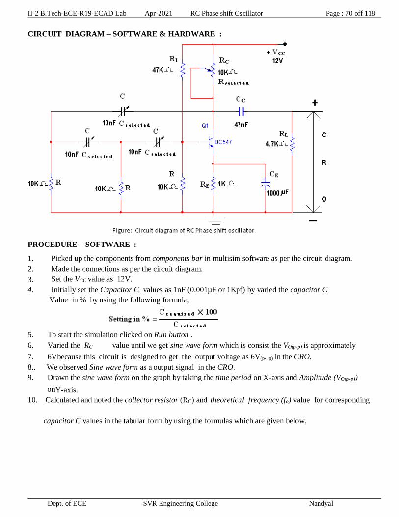
II-2 B.Tech-ECE-R19-ECAD Lab Apr-2021 RC Phase shift Oscillator Page : 70 off 118
Dept. of ECE SVR Engineering College Nandyal
CIRCUIT DIAGRAM – SOFTWARE & HARDWARE :
PROCEDURE – SOFTWARE :
1. Picked up the components from components bar in multisim software as per the circuit diagram.
2. Made the connections as per the circuit diagram.
3. Set the VCC value as 12V.
4. Initially set the Capacitor C values as 1nF (0.001µF or 1Kpf) by varied the capacitor C
Value in % by using the following formula,
5. To start the simulation clicked on Run button .
6. Varied the RC value until we get sine wave form which is consist the VO(p-p) is approximately
7. 6V because this circuit is designed to get the output voltage as 6V(p- p) in the CRO.
8.. We observed Sine wave form as a output signal in the CRO.
9. Drawn the sine wave form on the graph by taking the time period on X-axis and Amplitude (VO(p-p))
on Y-axis.
10. Calculated and noted the collector resistor (RC) and theoretical frequency (fo) value for corresponding
capacitor C values in the tabular form by using the formulas which are given below,
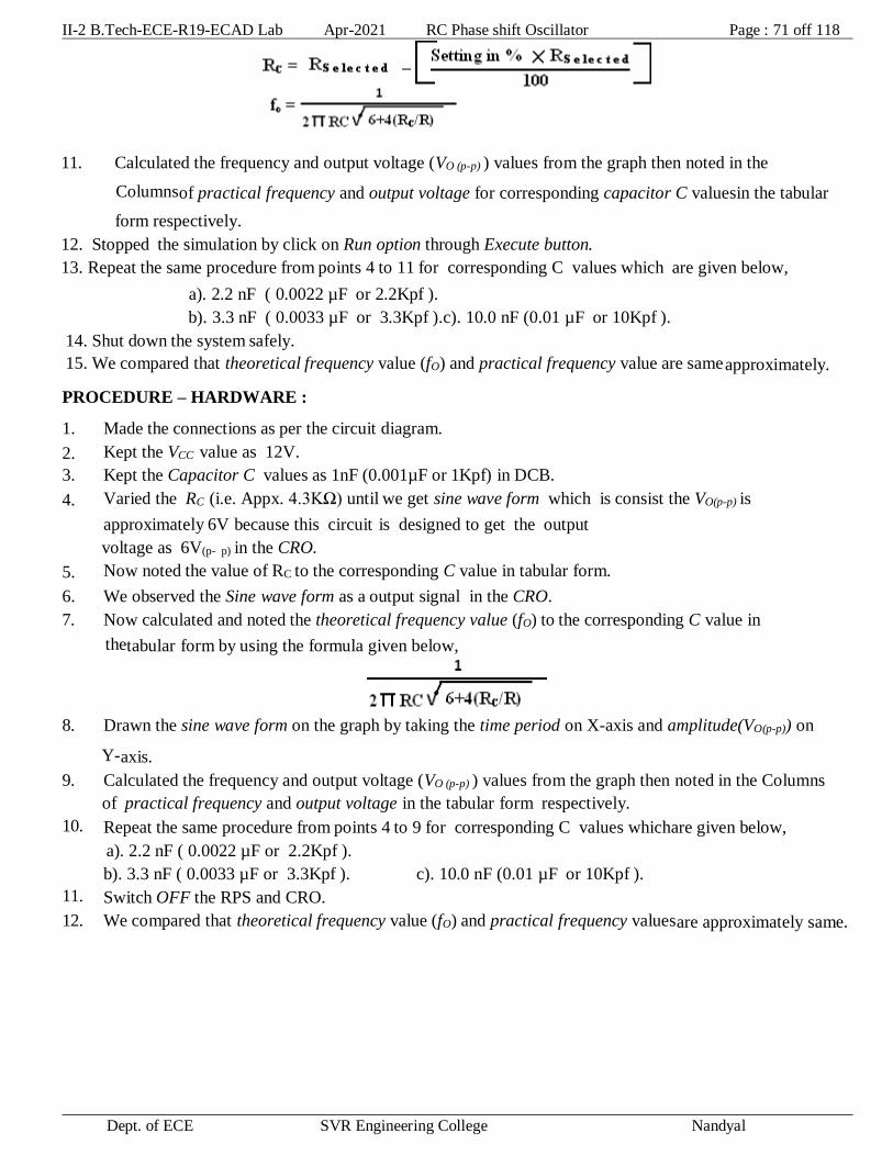
II-2 B.Tech-ECE-R19-ECAD Lab Apr-2021 RC Phase shift Oscillator Page : 71 off 118
Dept. of ECE SVR Engineering College Nandyal
11. Calculated the frequency and output voltage (VO (p-p) ) values from the graph then noted in the
Columns of practical frequency and output voltage for corresponding capacitor C valuesin the tabular
form respectively.
12. Stopped the simulation by click on Run option through Execute button.
13. Repeat the same procedure from points 4 to 11 for corresponding C values which are given below,
a). 2.2 nF ( 0.0022 µF or 2.2Kpf ).
b). 3.3 nF ( 0.0033 µF or 3.3Kpf ). c). 10.0 nF (0.01 µF or 10Kpf ).
14. Shut down the system safely.
15. We compared that theoretical frequency value (fO) and practical frequency value are same approximately.
PROCEDURE – HARDWARE :
1. Made the connections as per the circuit diagram.
2. Kept the VCC value as 12V.
3. Kept the Capacitor C values as 1nF (0.001µF or 1Kpf) in DCB.
4. Varied the RC (i.e. Appx. 4.3KΩ) until we get sine wave form which is consist the VO(p-p) is
approximately 6V because this circuit is designed to get the output
voltage as 6V(p- p) in the CRO.
5. Now noted the value of RC to the corresponding C value in tabular form.
6. We observed the Sine wave form as a output signal in the CRO.
7. Now calculated and noted the theoretical frequency value (fO) to the corresponding C value in
the tabular form by using the formula given below,
8. Drawn the sine wave form on the graph by taking the time period on X-axis and amplitude(VO(p-p)) on
Y- axis.
9. Calculated the frequency and output voltage (VO (p-p) ) values from the graph then noted in the Columns
of practical frequency and output voltage in the tabular form respectively.
10. Repeat the same procedure from points 4 to 9 for corresponding C values which are given below,
a). 2.2 nF ( 0.0022 µF or 2.2Kpf ).
b). 3.3 nF ( 0.0033 µF or 3.3Kpf ). c). 10.0 nF (0.01 µF or 10Kpf ).
11. Switch OFF the RPS and CRO.
12. We compared that theoretical frequency value (fO) and practical frequency values are approximately same.

II-2 B.Tech-ECE-R19-ECAD Lab Apr-2021 RC Phase shift Oscillator Page : 72 off 118
Dept. of ECE SVR Engineering College Nandyal
EXPECTED WAVEFORM – SOFTWARE & HARDWARE :
The following waveform shows the output signal for different capacitor values of RC phase shift Oscillator,
CALCULATIONS – SOFTWARE :
Sl.
No.
Rei
sto
r
(R)
In
KΩ
Capa-
citor
( C )
In
Kpf
RC = Rs e l e c t e d -
In
KΩ
Theoretical frequency
( fO)
In Hz/KHz.
Practical
Time
Period
(In
µS)
Pract-
Ical Fre
quency
In
Hz/KHz.
Output
Voltage
( VO(p-p))
In
Volts
1 10 1
2 10 2.2
3 10 3.3
4 10 10
CALCULATIONS – HARDWARE :
Sl.
No.
Reistor
(R)
In
KΩ
Capa-citor
( C )
In
Kpf
RC
In
KΩ
Theoretical frequency
( fO)
In Hz/KHz.
Practical
Time
Period
(InµS)
Pract-
Ical Fre
quency
In
Hz/KHz.
Output
Voltage
( VO(p-p))
In
Volts
1 10 1
2 10 2.2
3 10 3.3
4 10 10
RESULT : I have verified / drawn the output signal and calculated the frequency values of a given RC phase
shift oscillator.

II-2 B.Tech-ECE-R19-ECAD Lab Apr-2021 RC Phase shift Oscillator Page : 73 off 118
Dept. of ECE SVR Engineering College Nandyal
VIVA VOICE QUESTIONS:
1. What is positive feedback Amplifier?
2. State Barkhausen condition for oscillation.
3. What are the classifications of oscillators?
4. What are the types of RC oscillators?
5. What is the frequency of RC phase shift oscillator?
6. Applications of RC oscillators?
7. In RC phase shift oscillator, each RC section gives how much phase shift?
8. In AF oscillators which oscillators are used?

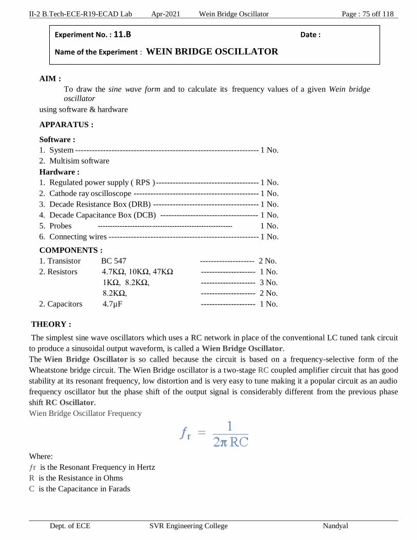
II-2 B.Tech-ECE-R19-ECAD Lab Apr-2021 Wein Bridge Oscillator Page : 75 off 118
Dept. of ECE SVR Engineering College Nandyal
AIM :
To draw the sine wave form and to calculate its frequency values of a given Wein bridge
oscillator
using software & hardware
APPARATUS :
Software :
1. System ------------------------------------------------------------------ 1 No.
2. Multisim software
Hardware :
1. Regulated power supply ( RPS ) ------------------------------------- 1 No.
2. Cathode ray oscilloscope --------------------------------------------- 1 No.
3. Decade Resistance Box (DRB) -------------------------------------- 1 No.
4. Decade Capacitance Box (DCB) ------------------------------------ 1 No.
5. Probes 1 No.
6. Connecting wires ------------------------------------------------------ 1 No.
COMPONENTS :
1. Transistor BC 547 -------------------- 2 No.
2. Resistors 4.7KΩ, 10KΩ, 47KΩ -------------------- 1 No.
1KΩ, 8.2KΩ, -------------------- 3 No.
8.2KΩ, -------------------- 2 No.
2. Capacitors 4.7µF -------------------- 1 No.
THEORY :
The simplest sine wave oscillators which uses a RC network in place of the conventional LC tuned tank circuit
to produce a sinusoidal output waveform, is called a Wien Bridge Oscillator.
The Wien Bridge Oscillator is so called because the circuit is based on a frequency-selective form of the
Wheatstone bridge circuit. The Wien Bridge oscillator is a two-stage RC coupled amplifier circuit that has good
stability at its resonant frequency, low distortion and is very easy to tune making it a popular circuit as an audio
frequency oscillator but the phase shift of the output signal is considerably different from the previous phase
shift RC Oscillator.
Wien Bridge Oscillator Frequency
Where:
ƒr is the Resonant Frequency in Hertz
R is the Resistance in Ohms
C is the Capacitance in Farads
Experiment No. : 11.B Date :
Name of the Experiment : WEIN BRIDGE OSCILLATOR

II-2 B.Tech-ECE-R19-ECAD Lab Apr-2021 Wein Bridge Oscillator Page : 76 off 118
Dept. of ECE SVR Engineering College Nandyal
Some of the applications of the Wein bridge oscillator as given below. These are highly
used for audio testing. Clock signals for testing filter circuits can be generated by this oscillator. Used in
distortion testing of power amplifiers.
Due to the advantages like good frequency stability, very low distortion and ease of
tuning, a Wien bridge oscillator becomes the most popular audio frequency range signal generator circuit.
CIRCUIT DIAGRAM :
PROCEDURE – SOFTWARE :
1. Picked up the components from components bar in multisim software as per the circuit diagram.
2. Made the connections as per the circuit diagram.
3. Set the VCC value as 12V.
4. Initially set the Capacitor C values as 1nF (0.001µF or 1Kpf) by varied the capacitor C
Value in % by using the following formula,
5. To start the simulation clicked on Run button .
6. Varied the R3 value until we get sine wave form which is consist the VO(p-p) is approximately 2.4V
because this circuit is designed to get the output voltage as 2.4V(p- p) in the CRO.
7.. We observed Sine wave form as a output signal in the CRO.
8. Drawn the sine wave form on the graph by taking the time period on X-axis and Amplitude (VO(p-p))
on Y-axis.

II-2 B.Tech-ECE-R19-ECAD Lab Apr-2021 Wein Bridge Oscillator Page : 77 off 118
Dept. of ECE SVR Engineering College Nandyal
9. Calculated and noted the resistor (R3) and theoretical frequency (fo) value for corresponding
capacitor C values in the tabular form by using the formulas which are given below,
10. Calculated the frequency and output voltage (VO (p-p) ) values from the graph then noted in the Columns
of practical frequency and output voltage for corresponding capacitor C valuesin the tabular form
respectively.
11. Stopped the simulation by click on Run option through Execute button.
12. Repeated the same procedure from points 4 to 11 for corresponding C values which are given below,
a). 10 nF ( 0.01µF/10Kpf ). b). 22 nF ( 0.022 µF/22Kpf ). c). 33 nF (0.033µF/33Kpf ).
13. Shut down the system safely.
14. We compared that theoretical frequency value (fO) and practical frequency value are
same approximately.
PROCEDURE – HARDWARE :
1. Calculated and noted the values of theoretical frequency(fo) values to the corresponding
capacitor C values in the tabular form by using the formula given below,
2. Made the connections as per the circuit diagram.
3. Switched ON the RPS and CRO.
4. Kept the VCC value as 12V in RPS.
5. Kept the Capacitor C value as 10nF (0.01µF or 10Kpf) in DCB and varied the R3 un till we
got sine wave form as output signal in the CRO.
6. Drawn the sine wave form on the graph by taking the time period on X-axis and amplitude(VO(p-
p)) on Y- axis.
7. Calculated the frequency and output voltage (VO (p-p) ) values from the graph then noted in the
columns of practical frequency and output voltage to the corresponding values in the tabular
form respectively.
8. Repeated the same procedure from steps points 5 to 7 for corresponding C alues which are given below,
a). 22 nF ( 0.022 µF/22Kpf b). 33 nF (0.033µF/33Kpf ).
9. Switch OFF the RPS and CRO.
10. I compared that theoretical frequency value (FO) and practical frequency values are approximately same.

II-2 B.Tech-ECE-R19-ECAD Lab Apr-2021 Wein Bridge Oscillator Page : 78 off 118
Dept. of ECE SVR Engineering College Nandyal
TABULAR FORM / CALCULATIONS - SOFTWARE :
Sl.
No.
R = Rs e l e c t e d -
In
KΩ
Capa-
citor
( C )
In
Kpf
Theoretical
frequency
( fO)
In Hz/KHz.
Practical
Time
Period
In
µS/mS
Pract-
Ical Fre
quency
In
Hz/KHz.
Output
Voltage
( VO(p-p))
In
Volts
1 10 0.52mS
2 22 1mS
3 33 1.6mS
TABULAR FORM / CALCULATIONS – HARDWARE :
Sl.No. Resistor (R)
In KΩ
Capacitor (C)
In Kpf/nF
Theoretical
Frequency (fO)
In Hz / KHz.
Practical
Time
Period
In µS/mS
Practical
Frequency
In
Hz./KHz.
Practical
Voltage
(VO(p-p))
In Volts
1
10
0.52mS
2
22
1mS
3
33
1.6mS
EXPECTED WAVEFORM :
The following waveform shows the output signal for Hartley Oscillator,
RESULT : I have drawn the output signal and calculated the frequency values of a given
Wein bridge Oscillator using software & hardware.

II-2 B.Tech-ECE-R19-ECAD Lab Apr-2021 Wein Bridge Oscillator Page : 79 off 118
Dept. of ECE SVR Engineering College Nandyal
VIVA VOICE Questions:
1. What is positive feedback Amplifier?
2. What are the conditions for oscillations?
3. What are the classifications of oscillators?
4. What are the types of RC oscillators?
5. What is the frequency of RC phase shift oscillator?
6. What is the frequency of Wien Bridge oscillator?
7. Applications of RC oscillators?
8. In RC phase shift oscillator, each RC section gives how much phase shift?
9. In Wien Bridge oscillator, feedback circuit gives how much phase shift?
10. In AF oscillators which oscillators are used?


II-2 B.Tech-ECE-R19-ECAD Lab Apr-2021 Colpitts Oscillator Page : 81 off 118
Dept. of ECE SVR Engineering College Nandyal
AIM :
To draw the sine wave form and to calculate its frequency values of a given Colpitts
Oscillator using software & hardware
APPARATUS :
Software :
1. System ------------------- 1 No.
2. Multisim software
Hardware :
1. Regulated power supply ( RPS ) ----------------------------- 1 No.
2. Cathode ray oscilloscope ------------------------------------- 1 No.
3. Decade Inductance Box ( DIB ) ----------------------------- 1 No.
4. Decade Capacitance (DCB) ---------------------- 1 No.
5. Bread board ---------------------- 1 No.
6. Probes ---------------------- 1 No.
7. Connecting wires ---------------------- 1 No.
COMPONENTS :
1. Transistor BC547 ---------------------- 1 No.
2. Resistors : 1KΩ, 1.5KΩ, 10KΩ, 47KΩ ------------- Each 1 No.
3. 0.1µF, 0.01µF ------------- Each 1 No.
THEORY :
The basic configuration of the Colpitts Oscillator resembles that of the Hartley Oscillator but the
difference this time is that the centre tapping of the tank sub-circuit is now made at the junction of a “capacitive
voltage divider” network instead of a tapped autotransformer type inductor as in the Hartley oscillator.
the resonant frequency of the LC tank circuit and is given as:
where CT is the capacitance of C1 and C2 connected in series and is given as:
The configuration of the transistor amplifier is of a Common Emitter Amplifier with the output
signal 180o out of phase with regards to the input signal. The additional 180o phase shift require for oscillation is
achieved by the fact that the two capacitors are connected together in series but in parallel with the inductive
coil resulting in overall phase shift of the circuit being zero or 360o.
Experiment No. : 12.A Date :
Name of the Experiment : COLPITTS OSCILLATOR

II-2 B.Tech-ECE-R19-ECAD Lab Apr-2021 Colpitts Oscillator Page : 82 off 118
Dept. of ECE SVR Engineering College Nandyal
CIRCUIT DIAGRAM – SOFTWARE & HARDWARE :
PROCEDURE - SOFTWARE :
1. First calculated the theoretical frequency for all capacitor C2 values by using the formula which is
available in the tabular form.
2. Picked up the components from components bar in multisim software as per the circuit diagram.
3. Made the connections as per the circuit diagram.
4. Set the VCC value as 12V.
5. Set the inductance(L) value as 5mH in DIB for all readings .
6. Initially set the Capacitor C values as 1nF (0.001µF/1Kpf/1nF) by varied the capacitor C Value in %
by using the following formula,
7. To start the simulation clicked on Run button .
8. We observed Sine wave form as a output signal in the CRO.
9. Drawn the sine wave form on the graph by taking the time period on X-axis and Amplitude (VO(p-p)) on Y-
axis.
10. Calculated the time period and output voltage (VO (p-p) ) values from the graph then noted in the Columns
of practical time period and output voltage for corresponding capacitor C2 values in the tabular form
respectively.

II-2 B.Tech-ECE-R19-ECAD Lab Apr-2021 Colpitts Oscillator Page : 83 off 118
Dept. of ECE SVR Engineering College Nandyal
11. Stopped the simulation by click on Run option through Execute button.
12. Repeated the same procedure from points 6 to 10 for corresponding C2 values which are given below,
a). 2.2 nF/2.2Kpf. b). 3.3 nF/3.3Kpf. c). 10.0 nF/10Kpf.
13. Shut down the system safely.
14. Now calculated the practical frequency by using formula 1/T and noted it in corresponding columns of C2
15. We compared that theoretical frequency value (fO) and practical frequency value are
same approximately.
PROCEDURE - HARDWARE :
1. Made the connections as per the circuit diagram.
2. Switched ON the RPS and CRO.
3. Set the VCC value as 12V in RPS.
4. Set the inductance(L) value as 5mH in DIB .
5. Set the Capacitor C2 value as 1nF (0.001µF or 1Kpf) in DCB. 6..
6. We observed Sine wave form as a output signal in the CRO.
7. Drawn the sine wave form on the graph by taking the time period on X-axis and amplitude(VO(p-p)) on
Y- axis.
8. Calculated the frequency and output voltage (VO (p-p) ) values from the graph then noted in the
columns of practical frequency and output voltage in the tabular form respectively.
9. Repeat the same procedure from points 5 to 7 for corresponding C2 values which are given below,
a). 2.2 nF ( 0.0022 µF or 2.2Kpf ). b). 3.3 nF ( 0.0033 µF or 3.3Kpf ).
7. Switch OFF the RPS and CRO.
8. Finally calculated and noted down the theoretical frequency value (FO) by using the formula,
1 / (2∏√(LCT) ) in the tabular form.
9. I compared that theoretical frequency value (FO) and practical frequency values are approximately same.
TABULAR FORM / CALCULATIONS – SOFTWARE :
Sl
No.
Capa
Citor
(C1)
Capa Citor
(C2)
Indu-
ctor.
(L)
In
mH
Total
Capaci-
tance (CT)
In nF
Theoretical
Frequency (fo) =
In
KHz
Pract-
ical –
Time-
Period.
In µS
Pract-
Ical
frequency
In KHz.
Output
voltage
(VO p-p)
In
Volts.
1. 10Kpf 1Kpf 5
2. 10Kpf 2.2Kpf 5
3. 10Kpf 3.3Kpf 5

II-2 B.Tech-ECE-R19-ECAD Lab Apr-2021 Colpitts Oscillator Page : 84 off 118
Dept. of ECE SVR Engineering College Nandyal
TABULAR FORM / CALCULATIONS – HARDWARE :
Sl
No.
Capa
Citor
(C1)
Capa
Citor
(C2)
Indu-
ctor.
(L)
In
mH
Total
Capaci-
tance (CT)
In nF
Theoretical
Frequency (fo) =
In
KHz
Pract-
ical –
Time-
Period.
In µS
Pract-
Ical
frequency
In KHz.
Output
voltage
(VO p-p)
In Volts.
1. 10Kpf 1Kpf 5
2. 10Kpf 2.2Kpf 5
3. 10Kpf 3.3Kpf 5
EXPECTED WAVEFORM – SOFTWARE & HARDWARE :
The following waveform shows the output signal for Colpitts Oscillator
RESULT : I have drawn the output signal and calculated the frequency values of a given Colpitts Oscillator.
II-2 B.Tech-ECE-R19-ECAD Lab Apr-2021 Colpitts Oscillator Page : 85 off 118
Dept. of ECE SVR Engineering College Nandyal
VIVA VOICE Questions:
1. What are LC oscillators?
2. What is the frequency of Colpitts oscillator?
3. What is the condition for sustained oscillation in Colpitts oscillator?
4. Applications of LC oscillators?
5. In Colpitts oscillator, feedback circuit consists of how many Inductors and capacitors?
6. Which type of feedback is used for Colpitts oscillator?
7. What is Q in Colpitts oscillator?
8. What is the advantage of Colpitts oscillator?
9. How does Colpitts oscillator calculate frequency?
10. What are the advantages and disadvantages of LC oscillator?

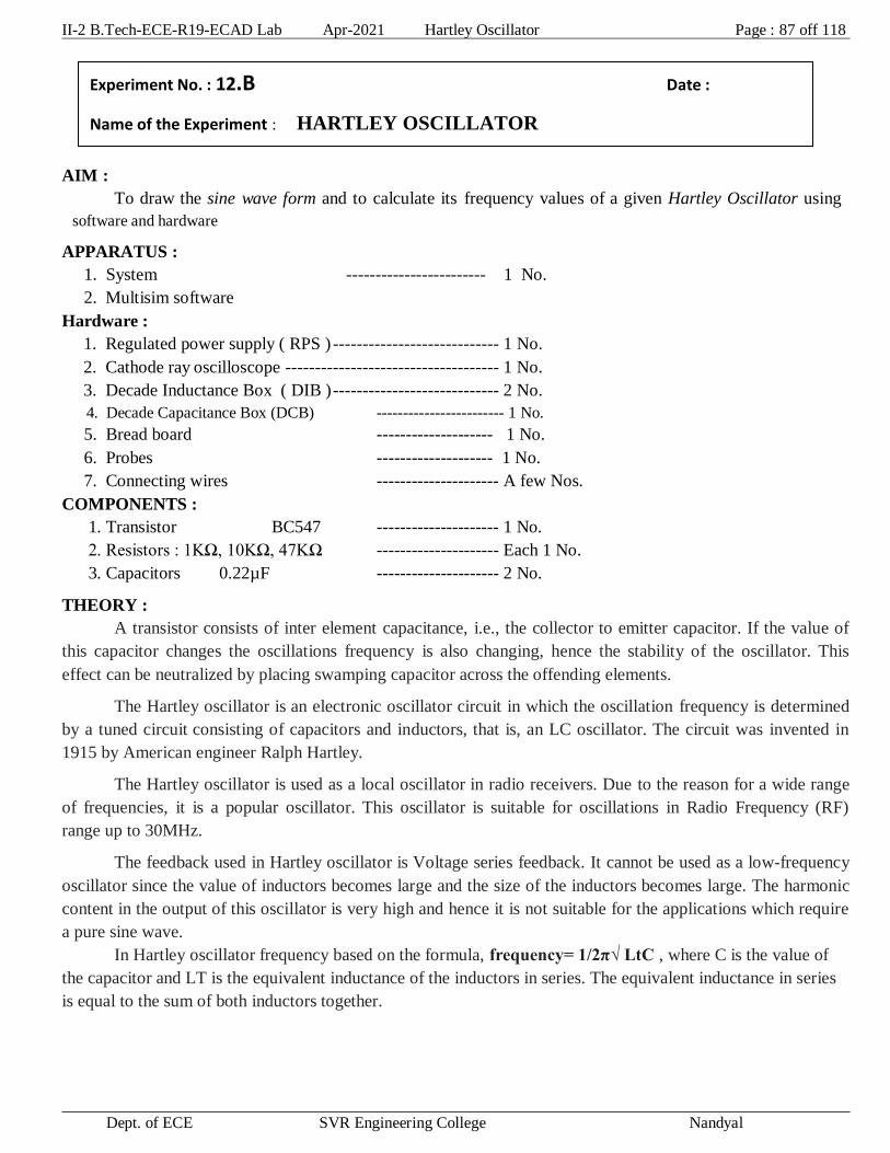
II-2 B.Tech-ECE-R19-ECAD Lab Apr-2021 Hartley Oscillator Page : 87 off 118
Dept. of ECE SVR Engineering College Nandyal
AIM :
To draw the sine wave form and to calculate its frequency values of a given Hartley Oscillator using
software and hardware
APPARATUS :
1. System ------------------------ 1 No.
2. Multisim software
Hardware :
1. Regulated power supply ( RPS ) ---------------------------- 1 No.
2. Cathode ray oscilloscope ------------------------------------ 1 No.
3. Decade Inductance Box ( DIB ) ---------------------------- 2 No.
4. Decade Capacitance Box (DCB) ------------------------ 1 No.
5. Bread board -------------------- 1 No.
6. Probes -------------------- 1 No.
7. Connecting wires --------------------- A few Nos.
COMPONENTS :
1. Transistor BC547 --------------------- 1 No.
2. Resistors : 1KΩ, 10KΩ, 47KΩ --------------------- Each 1 No.
3. Capacitors 0.22µF --------------------- 2 No.
THEORY :
A transistor consists of inter element capacitance, i.e., the collector to emitter capacitor. If the value of
this capacitor changes the oscillations frequency is also changing, hence the stability of the oscillator. This
effect can be neutralized by placing swamping capacitor across the offending elements.
The Hartley oscillator is an electronic oscillator circuit in which the oscillation frequency is determined
by a tuned circuit consisting of capacitors and inductors, that is, an LC oscillator. The circuit was invented in
1915 by American engineer Ralph Hartley.
The Hartley oscillator is used as a local oscillator in radio receivers. Due to the reason for a wide range
of frequencies, it is a popular oscillator. This oscillator is suitable for oscillations in Radio Frequency (RF)
range up to 30MHz.
The feedback used in Hartley oscillator is Voltage series feedback. It cannot be used as a low-frequency
oscillator since the value of inductors becomes large and the size of the inductors becomes large. The harmonic
content in the output of this oscillator is very high and hence it is not suitable for the applications which require
a pure sine wave.
In Hartley oscillator frequency based on the formula, frequency= 1/2π√ LtC , where C is the value of
the capacitor and LT is the equivalent inductance of the inductors in series. The equivalent inductance in series
is equal to the sum of both inductors together.
Experiment No. : 12.B Date :
Name of the Experiment : HARTLEY OSCILLATOR

II-2 B.Tech-ECE-R19-ECAD Lab Apr-2021 Hartley Oscillator Page : 88 off 118
Dept. of ECE SVR Engineering College Nandyal
CIRCUIT DIAGRAM :
PROCEDURE - SOFTWARE :
1. First calculated the theoretical frequency for all capacitor C values by using the formula
which is available in the tabular form.
2. Picked up the components from components bar in multisim software as per the circuit diagram.
3. Made the connections as per the circuit diagram.
4. Set the VCC value as 12V.
5. Set the inductance L1 & L2 values as 5mH in both DIB’s for all readings .
6. Initially set the Capacitor C values as 10nF (0.01µF/10Kpf/10nF) by varied the capacitor C
Value in % by using the following formula,
7. To start the simulation clicked on Run button .
8. We observed Sine wave form as a output signal in the CRO.
9. Drawn the sine wave form on the graph by taking the time period on X-axis and Amplitude (VO(p-
p)) on Y-axis.

II-2 B.Tech-ECE-R19-ECAD Lab Apr-2021 Hartley Oscillator Page : 89 off 118
Dept. of ECE SVR Engineering College Nandyal
10.Calculated the time period and output voltage (VO (p-p) ) values from the graph then noted in
the Columns of practical time period and output voltage for corresponding capacitor C
values in the tabular form respectively.
11. Stopped the simulation by click on Run option through Execute button.
12. Repeated the same procedure from points 6 to 10 for corresponding C2 values which are given
below, a). 33nF/33Kpf. b). 47 nF/47Kpf.
13. Shut down the system safely.
14. Now calculated the practical frequency by using formula 1/T and noted it in corresponding
columns of C
15. We compared that theoretical frequency value (fO) and practical frequency value are
same approximately.
PROCEDURE - HARDWARE :
1. Calculated and noted the values of theoretical frequency(fo) values to the corresponding
capacitor C
values in the tabular form by using the formula given below,
2. Made the connections as per the circuit diagram.
3. Switched ON the RPS and CRO.
4. Kept the VCC value as 12V in RPS.
5. Kept the Capacitor C value as 10nF (0.01µF or 10Kpf) in DCB and 5mH in both
Inductors and maintained the 5mH value as a constant in both DIB’s up to the experiment is
completed..
6. I observed Sine wave form as a output signal in the CRO.
7. Drawn the sine wave form on the graph by taking the time period on X-axis and amplitude(VO(p-p))
on Y- axis.
8. Calculated the frequency and output voltage (VO (p-p) ) values from the graph then noted in the
columns of practical frequency and output voltage to the corresponding values in the tabular
form respectively.
9. Repeated the same procedure from points 6 to 8 for corresponding C valu which are given below,
a). 33nF ( 0.01 µF or
33Kpf ). b). 47nF ( 0.047
µF or 47Kpf ).
10. Switch OFF the RPS and CRO.
11. I compared that theoretical frequency value (FO) and practical frequency values are approximately
same.
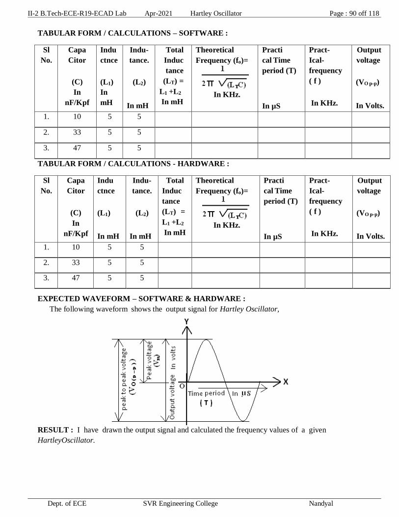
II-2 B.Tech-ECE-R19-ECAD Lab Apr-2021 Hartley Oscillator Page : 90 off 118
Dept. of ECE SVR Engineering College Nandyal
TABULAR FORM / CALCULATIONS – SOFTWARE :
Sl
No.
Capa
Citor
(C)
In
nF/Kpf
Indu
ctnce
(L1)
In
mH
Indu-
tance.
(L2)
In mH
Total
Induc
tance
(LT) =
L1 +L2
In mH
Theoretical
Frequency (fo)=
In KHz.
Practi
cal Time
period (T)
In µS
Pract-
Ical-
frequency
( f )
In KHz.
Output
voltage
(VO p-p)
In Volts.
1. 10 5 5
2. 33 5 5
3. 47 5 5
TABULAR FORM / CALCULATIONS - HARDWARE :
Sl
No.
Capa
Citor
(C)
In
nF/Kpf
Indu
ctnce
(L1)
In mH
Indu-
tance.
(L2)
In mH
Total
Induc
tance
(LT) =
L1 +L2
In mH
Theoretical
Frequency (fo)=
In KHz.
Practi
cal Time
period (T)
In µS
Pract-
Ical-
frequency
( f )
In KHz.
Output
voltage
(VO p-p)
In Volts.
1. 10 5 5
2. 33 5 5
3. 47 5 5
EXPECTED WAVEFORM – SOFTWARE & HARDWARE :
The following waveform shows the output signal for Hartley Oscillator,
RESULT : I have drawn the output signal and calculated the frequency values of a given
Hartley Oscillator.

II-2 B.Tech-ECE-R19-ECAD Lab Apr-2021 Hartley Oscillator Page : 91 off 118
Dept. of ECE SVR Engineering College Nandyal
VIVA VOICE Questions:
1. What is positive feedback Amplifier?
2. What are the conditions for oscillations?
3. What are the classifications of oscillators?
4. What are the types of LC oscillators?
5. What is the frequency of Hartley oscillator?
6. Applications of LC oscillators?
7. In Hartley oscillator, feedback circuit consists of how many Inductors and capacitors?
8. In RF oscillators which oscillators are used?
9. Why Hartley oscillator is used?
10. Why Hartley oscillator is used?

II-2 B.Tech-ECE-R19-ECAD Lab Apr-2021 Bootstraped Emitter follower Page : 93 off 118
Dept. of ECE SVR Engineering College Nandyal
AIM :
To obtain the frequency response of Bootstrapped Emitter Follower using software and hardware
APPARATUS :
1. System --------------------------------------------------------------------- 1 No.
2. Multisim software
APPARATUS :
1. Regulated power supply ( RPS ) ----------------------------------- 1 No.
2. Cathode Ray Oscilloscope ( CRO) ----------------------------------- 1 No.
3. Function generator ------------------------------------------------------- 1 No.
4. Probes ---------------------------------------------------------------------- 1 No.
5. Bread board --------------------------------------------------------------- 1 No.
6. Connecting wires --------------------------------------------------------- A few Nos.
COMPONENTS :
1. Transistor BC 547 -------------------------------------------------------- 2 No.
2. Capacitors :
ii). 10 µF ------------------------------------------------------------------- 2 No.
i). 22 µF ----------------------------------------------------------------- 1 No.
3. Resistors :
i). 100 KΩ --------------------------------------------------------------- 2 No.
ii). 10 KΩ --------------------------------------------------------------- 2 No.
iii). 100 Ω --------------------------------------------------------------- 2 No
THEORY :
Typically Bootstrapping is technique where some part of output is used at the startup. In Bootstrap
amplifier, bootstrapping is used to increase the input impedance. Due to which the loading effect on the input
source also decreases. The design looks similar to the Darlington pair, having a bootstrap capacitor. Bootstrap
capacitor is used to provide AC signal’s positive feedback to the base of the transistor. This positive feedback
help in improving the effective value of the base resistance. This increment in the base resistance also
determined by the voltage gain of the amplifier circuit.
High input impedance improves the amplification of the input signal and thus required in various
amplifier applications. If we have low input impedance we will get low amplification. Generally, BJT (Bipolar
Junction Transistor) have low input impedance (typically 1 ohm to 50 kilo ohm). So for this, bootstrapping
technique is used to increase the input impedance.
The voltage across the input impedance is calculated by using the below formula:
V = (Vin.Zin) / (Vin + Z.Vin)
Hence, according to the formula, the input impedance is proportional to the voltage across it. If the input
impedance is increased the voltage across it will also increase and vice versa.
Experiment No. : 13 Date :
Name of the Experiment : BOOTSTRAPPED EMITTER FOLLOWER (Beyond the Syllabus-Using Software & Hardware)

II-2 B.Tech-ECE-R19-ECAD Lab Apr-2021 Bootstraped Emitter follower Page : 94 off 118
Dept. of ECE SVR Engineering College Nandyal
CIRCUIT DIAGRAM – SOFTWARE & HARDWARE :
PROCEDURE – SOFTWARE :
1. We have picked up the components from the components bar as per above circuit.
2. Made the connections as per the above circuit diagram by using the components which we have picked
up.
3. Connected the CRO across the Emitter capacitor to ground.
4. Set the input signal as sine wave form which is having the value 20mVP-P as constant in the function
generator.
5. Initially set the input signal frequency value is 1KHz in the function generator.
6. To simulate the circuit clicked on run option through execute button in tool bar.
7. We have seen the sine wave on the CRO screen as o/p signal.
8. Calculated the peak to peak voltage (VO(p-p)) and noted down in the tabular form Against the column of
1KHz.
9. Stopped the simulation by clicked on run option through execute button in the tool bar.
10. Repeat the same procedure from points 6 to 9 for the corresponding frequency values by setting in the
function generator for the steps of 10Hz, 500Hz, 1KHz, 100KHz, 200KHz, 400KHz,600KHz, 1180KHz,
1MHz, 100MHz, 500MHz. in the function generator.
11. Observed the graph for frequency Vs amplitude through the AC Analysis.
12. Finally shut down the system safely.
13. We have observed that, the graph which is drawn by manually is same to the graph which is obtained from
the AC Analysis.
14. Now calculated and noted down the values of voltage gain(AV) and gain in dB to the corresponding values
of output voltage(VO) & input voltage(Vi) by using the formulas given below,
Voltage gain (Av) = Vo / Vi and Gain in dB = 20log10(Av).
15). Plotted the graphs (frequency response curves) as per below
a). frequency on X-axis & gain in dB on Y-axis.
b). frequency on X-axis & voltage gain on Y-axis.
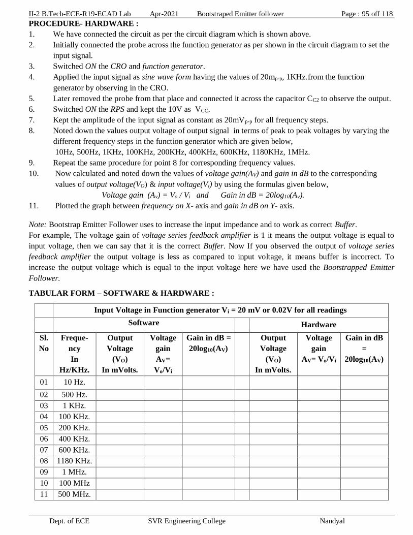
II-2 B.Tech-ECE-R19-ECAD Lab Apr-2021 Bootstraped Emitter follower Page : 95 off 118
Dept. of ECE SVR Engineering College Nandyal
PROCEDURE- HARDWARE :
1. We have connected the circuit as per the circuit diagram which is shown above.
2. Initially connected the probe across the function generator as per shown in the circuit diagram to set the
input signal.
3. Switched ON the CRO and function generator.
4. Applied the input signal as sine wave form having the values of 20mp-p, 1KHz.from the function
generator by observing in the CRO.
5. Later removed the probe from that place and connected it across the capacitor CC2 to observe the output.
6. Switched ON the RPS and kept the 10V as VCC.
7. Kept the amplitude of the input signal as constant as 20mVp-p for all frequency steps.
8. Noted down the values output voltage of output signal in terms of peak to peak voltages by varying the
different frequency steps in the function generator which are given below,
10Hz, 500Hz, 1KHz, 100KHz, 200KHz, 400KHz, 600KHz, 1180KHz, 1MHz.
9. Repeat the same procedure for point 8 for corresponding frequency values.
10. Now calculated and noted down the values of voltage gain(AV) and gain in dB to the corresponding
values of output voltage(VO) & input voltage(Vi) by using the formulas given below,
Voltage gain (Av) = Vo / Vi and Gain in dB = 20log10(Av).
11. Plotted the graph between frequency on X- axis and gain in dB on Y- axis.
Note: Bootstrap Emitter Follower uses to increase the input impedance and to work as correct Buffer.
For example, The voltage gain of voltage series feedback amplifier is 1 it means the output voltage is equal to
input voltage, then we can say that it is the correct Buffer. Now If you observed the output of voltage series
feedback amplifier the output voltage is less as compared to input voltage, it means buffer is incorrect. To
increase the output voltage which is equal to the input voltage here we have used the Bootstrapped Emitter
Follower.
TABULAR FORM – SOFTWARE & HARDWARE :
Input Voltage in Function generator Vi = 20 mV or 0.02V for all readings
Software Hardware
Sl.
No
Freque-
ncy
In
Hz/KHz.
Output
Voltage
(VO)
In mVolts.
Voltage
gain
AV=
Vo/Vi
Gain in dB =
20log10(AV)
Output
Voltage
(VO)
In mVolts.
Voltage
gain
AV= Vo/Vi
Gain in dB
=
20log10(AV)
01 10 Hz.
02 500 Hz.
03 1 KHz.
04 100 KHz.
05 200 KHz.
06 400 KHz.
07 600 KHz.
08 1180 KHz.
09 1 MHz.
10 100 MHz
11 500 MHz.
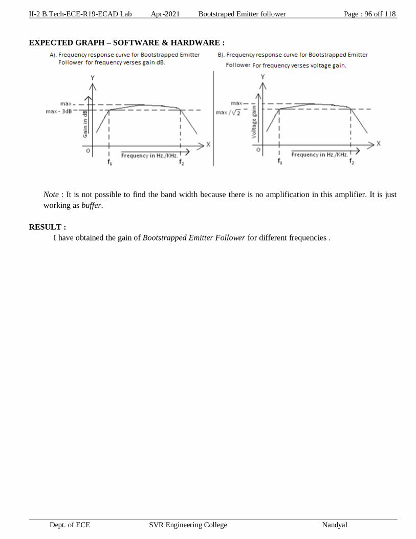
II-2 B.Tech-ECE-R19-ECAD Lab Apr-2021 Bootstraped Emitter follower Page : 96 off 118
Dept. of ECE SVR Engineering College Nandyal
EXPECTED GRAPH – SOFTWARE & HARDWARE :
Note : It is not possible to find the band width because there is no amplification in this amplifier. It is just
working as buffer.
RESULT :
I have obtained the gain of Bootstrapped Emitter Follower for different frequencies .
II-2 B.Tech-ECE-R19-ECAD Lab Apr-2021 Bootstraped Emitter follower Page : 97 off 118
Dept. of ECE SVR Engineering College Nandyal
VIVA VOICE Questions:
1. What is bootstrapped emitter follower?
2. Effect of bootstrapping in amplifier circuit ?
3. How to determine the input resistance of a bootstrapped emitter follower ?
4. What is the need of boot strap emitter follower ?
5. What is the effect of bootstrap technique on emitter follower?
6. What is bootstrapped Darlington circuit?
7. What is a bootstrapped supply?

II-2 B.Tech-ECE-R19-ECAD Lab Apr-2021 Astable Multivibrator Page : 99 off 118
Dept. of ECE SVR Engineering College Nandyal
AIM :
To conduct and verify the Astable multi vibrator and to draw the waveforms using software and hardware
APPARATUS :
1. System with Multisim software ------------------------- 1 No.
2. Regulated power supply ( RPS ) ------------------------- 1 No.
3. Cathode ray oscilloscope --------------------------------- 1 No.
4. Function Generator ------------------------ 1 No.
5. Bread board ------------------------------------------------ 1 No.
6. Probes ------------------------------------------------------ 1 No.
7. Connecting wires ------------------------------------------ 1 No.
COMPONENTS :
1. Resistors : 1KΩ -------------------------------------- 2 No.
10 KΩ -------------------------------------- 2 No.
100 KΩ ------------------------------------- 2 No.
2. Capacitors : 0.1µF / 100nF ---------------------------- 2 No.
3. Transistor : BC547 ------------------------------------- 2 No.
THEORY :
Astable Multivibrator is a two stage switching circuit in which the output of the first stage is fed to the
input of the second stage and vice versa. The outputs of both the stages are complementary. This free running
multivibrator generates square wave without any external triggering pulse.
It is also called free-running relaxation oscillator. It has no stable state but only two quasi-stable states
between which it keeps oscillating continuously of its own accord without any external excitation. When one
transistor is in ON state and other remains in OFF state.
As a timing oscillator or clock of a computer system. It is also used for a flashing lights, switching and
power supply circuits.
Advantages :
1. They work consistently and are not influenced by any outside forces or events.
2. They are inexpensive.
3. They are simple in design.
4. They can remain functional for an extraordinary length of time.
Disadvantages :
They do not transfer the entire output signal to the input due to several reasons like:
1. There is resistance within the circuit.
2. Absence of a completely closed loop at the output terminals.
3. One capacitor or transistor has a tendency to absorb energy at a slightly different rate than the other.
4. Even though the amplifier restores the lost energy when it amplifies the signal, the signal is too small.
Experiment No. : 14 Date :
Name of the Experiment : ASTABLE MULTIVIBRATOR (Beyond the Syllabus-Using Software & Hardware)

II-2 B.Tech-ECE-R19-ECAD Lab Apr-2021 Astable Multivibrator Page : 100 off 118
Dept. of ECE SVR Engineering College Nandyal
CIRCUIT DIAGRAMS – SOFTWARE & HARDWARE:
Design Procedure :
The period T is given by T = T1 + T2 = 0.69 (R1C1 + R2C2)
For symmetrical circuit, with R1 = R2 = R & C1 = C2 = C
T = 1.38 RC
Let VCC = 12V; hfe = 51 (for BC107), VBESat = 0.7V; VCESat = 0.3V Let C = 0.1 F & T = 1mSec.
10-3 = 1.38 x R X 0.1 X 10⁻⁶
R = 7.24K (Practically choose 10K ) i.e., R1 and R2 resistors = 10KΩ
Let ICmax = 10mA
RC = = 1.17K ( Practically choose 1KΩ ) i.e., Rc1 and Rc2 resistors =
1KΩ
Theoretical calculations :
F = 1/ T = (1/1.38RC)
R = 10K C = 0.1 F
II-2 B.Tech-ECE-R19-ECAD Lab Apr-2021 Astable Multivibrator Page : 101 off 118
Dept. of ECE SVR Engineering College Nandyal
PROCEDURE - SOFTWARE :
1. I have picked up the components from the components bar as per above circuit.
2. Made the connections as per the above circuit diagram by using the components which we have picked
up.
3. Connected the CRO across VC1 and VC2 .
6. To simulate the circuit clicked on run option through execute button in tool bar.
7. I have observed the wave forms as shown under the heading of Expected graphs .
8. Observed the Base Voltage and Collector Voltages of Q1 & Q2 on CRO in DC mode and measured
the frequency (f = 1/T).
9. Traced the waveforms at collector and base as each transistor with the help of dual trace CRO and plot the
waveforms.
10. Verified the practical output frequency with theoretical values f = 1/T, where T = 1.38RC
11. Shut down the system safely.
12. Plotted the graphs for VB1 & VC1 and VB2 and VC2 by taking the Time period on X-axis and Voltage on
Y-axis for all graphs as per shown in the Expected graphs heading.
13. Noted the practical Time period T values at VB1 & VC1 and VB2 and VC2 and noted down in the
corresponding columns of the Tabular form.
14. Calculated the practical frequency values by using formula 1/T and noted down in the corresponding
columns of the Tabular form.
15. I Compared the Theoretical and practical values are approximately same.
PROCEDURE - HARDWARE :
1. I have made the connections as per the circuit diagram.
2. Observed the Base Voltage and Collector Voltages of Q1 & Q2 on CRO in DC mode and measured
the frequency (f = 1/T).
3. Traced the waveforms at collector and base as each transistor with the help of dual
trace CRO and plot the waveforms.
4. Verified the practical output frequency with theoretical values f = 1/T, where T = 1.38RC
5. Switched off the RPS and CRO.
6. Plotted the graphs for VB1 & VC1 and VB2 and VC2 by taking the Time period on X-axis and Voltage on
Y-axis for all graphs as per shown in the Expected graphs heading.
7. Noted the practical Time period T values at VB1 & VC1 and VB2 and VC2 and noted down in the
corresponding columns of the Tabular form.
8. Calculated the practical frequency values by using formula 1/T and noted down in the corresponding
columns of the Tabular form.
9. I Compared the Theoretical and practical values are approximately same.
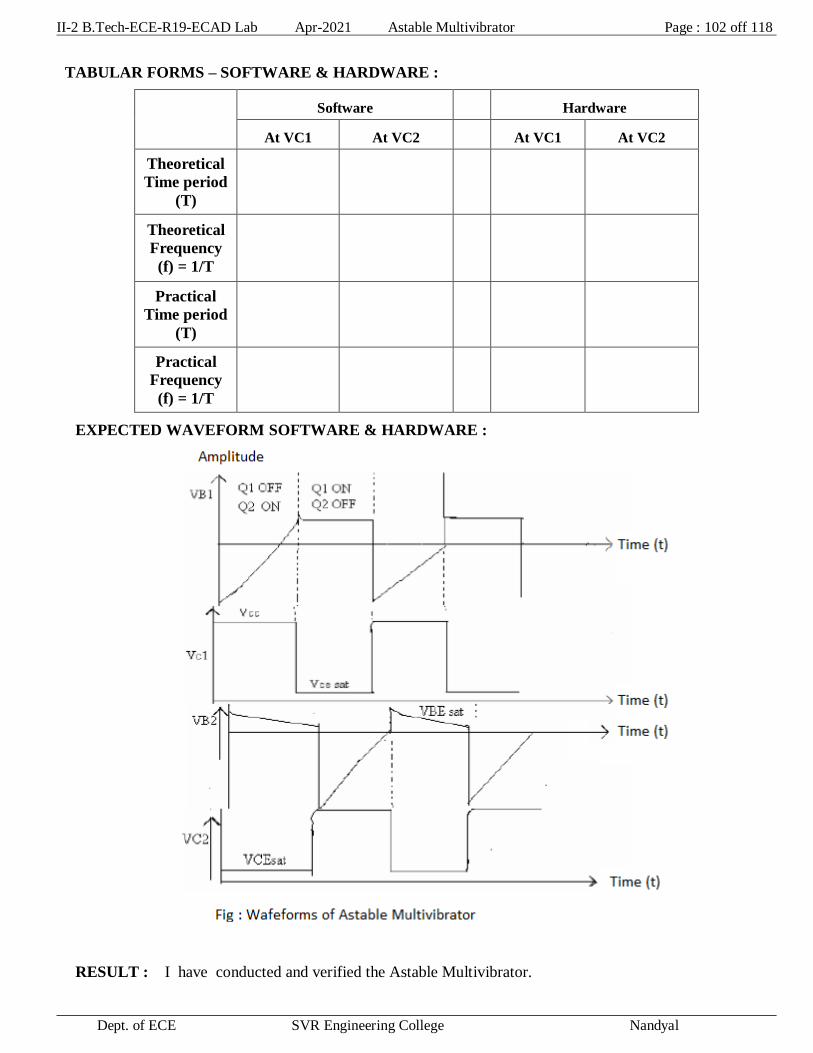
II-2 B.Tech-ECE-R19-ECAD Lab Apr-2021 Astable Multivibrator Page : 102 off 118
Dept. of ECE SVR Engineering College Nandyal
TABULAR FORMS – SOFTWARE & HARDWARE :
Software Hardware
At VC1 At VC2 At VC1 At VC2
Theoretical
Time period
(T)
Theoretical
Frequency
(f) = 1/T
Practical
Time period
(T)
Practical
Frequency
(f) = 1/T
EXPECTED WAVEFORM SOFTWARE & HARDWARE :
RESULT : I have conducted and verified the Astable Multivibrator.

II-2 B.Tech-ECE-R19-ECAD Lab Apr-2021 Astable Multivibrator Page : 103 off 118
Dept. of ECE SVR Engineering College Nandyal
VIVA VOICE Questions:
1. What is Multi-vibrator?
2. What are the types of Multi-vibrators?
3. What is Astable Multi-vibrator?
4. Mention the Applications of Astable Multi-vibrator.
5. Astable Multi-vibrator is having how many stable states?
6. Which one is Square wave oscillator?
7. Which of the multi-vibrator used in Relaxation oscillators?
11. Compare Mono-stable, Bi-stable and Astable multi-vibrators.
12. What is Quasi stable?
13. Free running Multi vibrator generates Square wave. ( True or False)


II-2 B.Tech-ECE-R19-ECAD Lab Apr-2021 Data sheets Page : 105 off 118
Dept. of ECE SVR Engineering College Nandyal
A. DATA SHEETS
PN JUNCTION DIODE :
Maximum Ratings and Electrical Characteristics (@TA = +25°C unless otherwise specified.) Single phase, half wave,
For capacitive load, derate current by 20%.
Characteristic Symbol 1N4001 1N4002 1N4003 1N4004 1N4005 1N4006 1N4007 Unit
Peak Repetitive Reverse Voltage
Working Peak Reverse Voltage DC
Blocking Voltage
VRRM
VRW
M VR
50
100
200
400
1180
1180
1000
V
RMS Reverse Voltage VR(RMS) 35 70 140 2118 420 5118 700 V
Average Rectified Output Current (Note 1) @ TA =+75C IO 1.0 A
Non-Repetitive Peak Forward Surge Current 8.3ms Single Half Sine-Wave Superimposed on Rated Load
IFSM
30
A
Forward Voltage @ IF = 1.0A VFM 1.0 V
Peak Reverse Current @TA = +25C at Rated DC Blocking Voltage @ TA = +100C
IRM
5.0
50
A
Typical Junction Capacitance (Note 2) Cj 15 8 pF
Typical Thermal Resistance Junction to Ambient RJA 100 K/W
Maximum DC Blocking Voltage Temperature TA +150 C
Operating and Storage Temperature Range TJ, TSTG -65 to +150 C
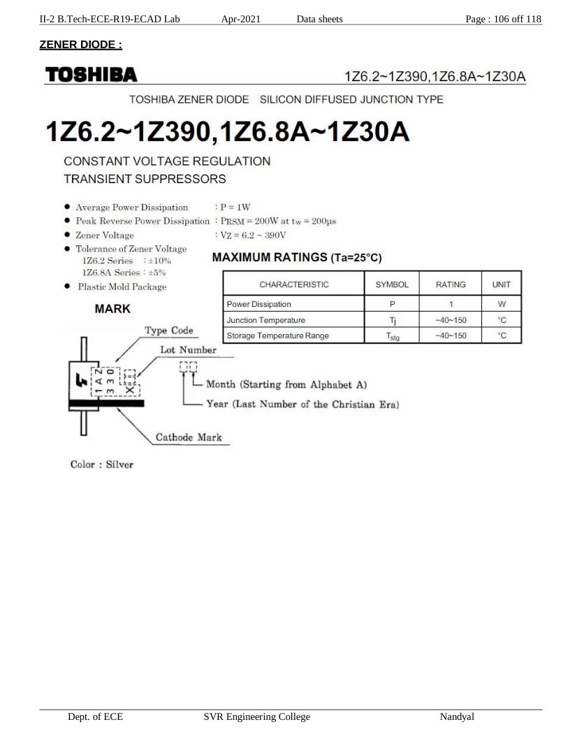
II-2 B.Tech-ECE-R19-ECAD Lab Apr-2021 Data sheets Page : 106 off 118
Dept. of ECE SVR Engineering College Nandyal
ZENER DIODE :
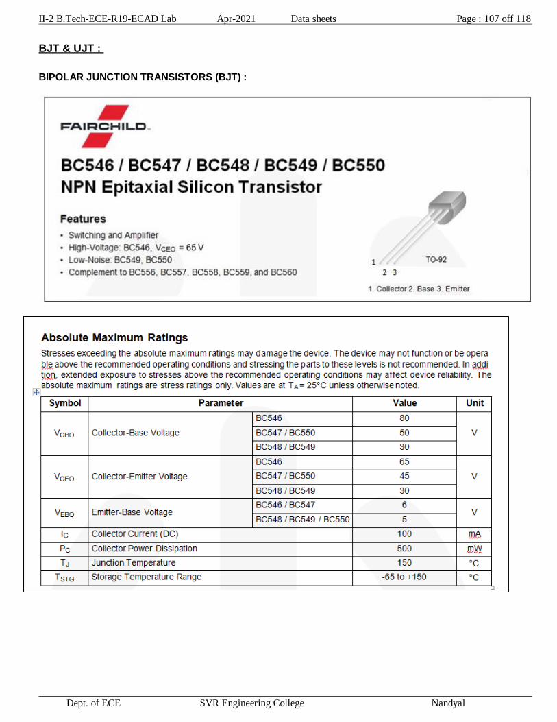
II-2 B.Tech-ECE-R19-ECAD Lab Apr-2021 Data sheets Page : 107 off 118
Dept. of ECE SVR Engineering College Nandyal
BJT & UJT :
BIPOLAR JUNCTION TRANSISTORS (BJT) :

II-2 B.Tech-ECE-R19-ECAD Lab Apr-2021 Data sheets Page : 108 off 118
Dept. of ECE SVR Engineering College Nandyal

II-2 B.Tech-ECE-R19-ECAD Lab Apr-2021 Data sheets Page : 109 off 118
Dept. of ECE SVR Engineering College Nandyal
UNIJUNCTION TRANSISTOR (UJT) :
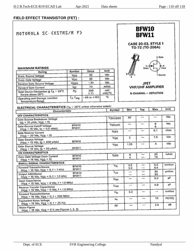
II-2 B.Tech-ECE-R19-ECAD Lab Apr-2021 Data sheets Page : 110 off 118
Dept. of ECE SVR Engineering College Nandyal
FIELD EFFECT TRANSISTOR (FET) :
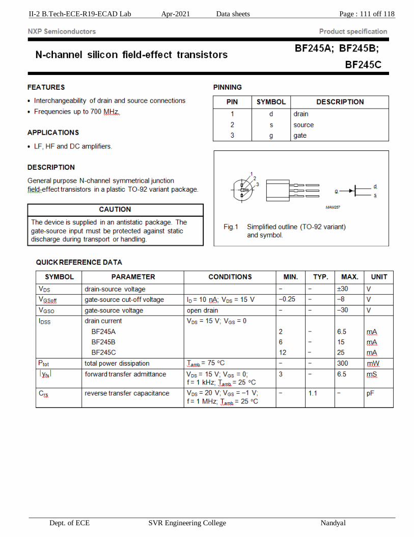
II-2 B.Tech-ECE-R19-ECAD Lab Apr-2021 Data sheets Page : 111 off 118
Dept. of ECE SVR Engineering College Nandyal

II-2 B.Tech-ECE-R19-ECAD Lab Apr-2021 Data sheets Page : 112 off 118
Dept. of ECE SVR Engineering College Nandyal
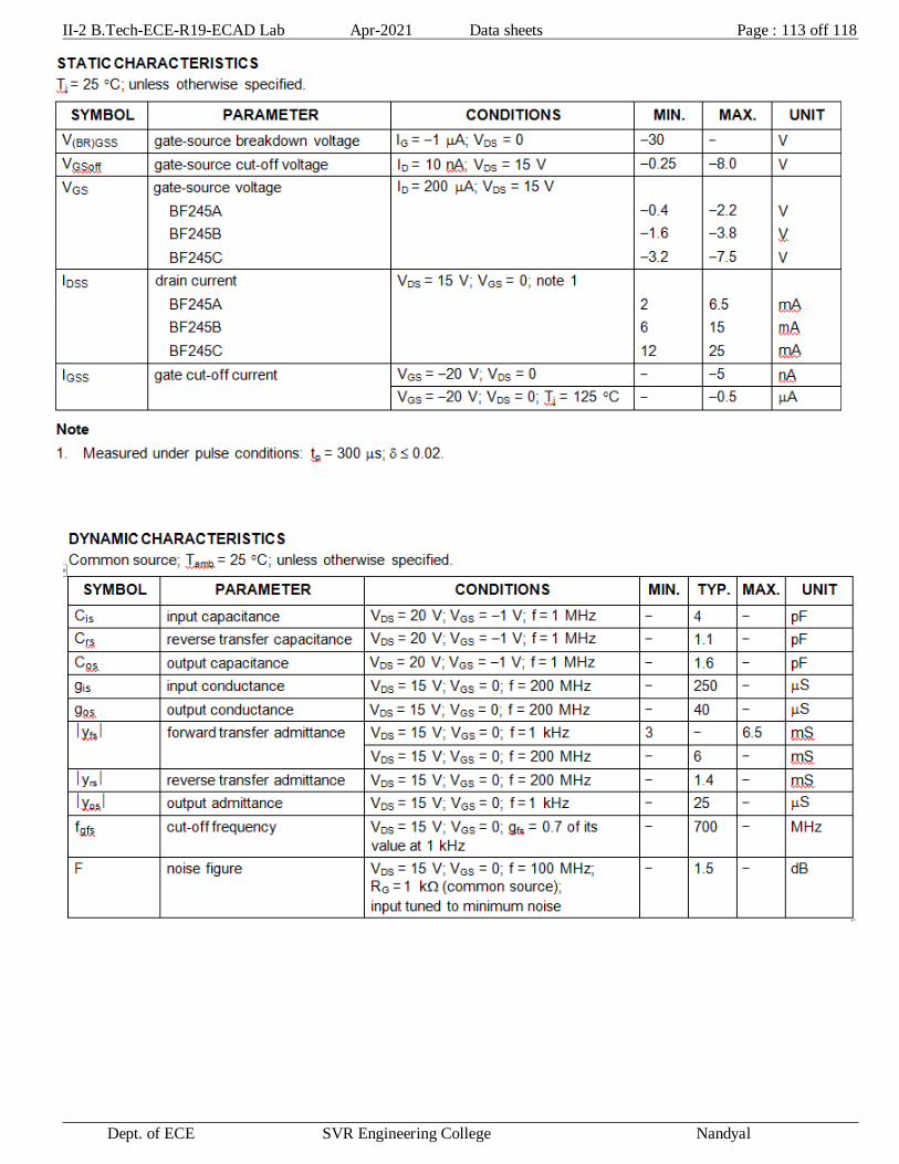
II-2 B.Tech-ECE-R19-ECAD Lab Apr-2021 Data sheets Page : 113 off 118
Dept. of ECE SVR Engineering College Nandyal

II-2 B.Tech-ECE-R19-ECAD Lab Apr-2021 Data sheets Page : 114 off 118
Dept. of ECE SVR Engineering College Nandyal
MOSFET IRFZ 44N

II-2 B.Tech-ECE-R19-ECAD Lab Apr-2021 Data sheets Page : 115 off 118
Dept. of ECE SVR Engineering College Nandyal

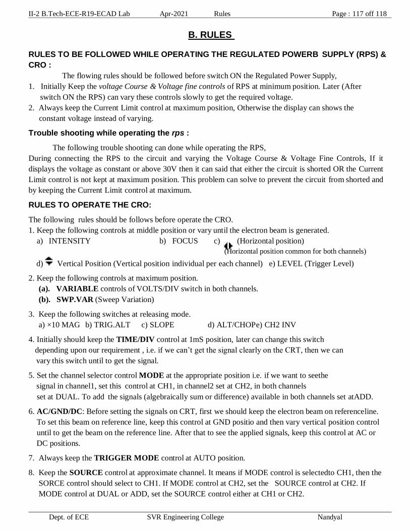
II-2 B.Tech-ECE-R19-ECAD Lab Apr-2021 Rules Page : 117 off 118
Dept. of ECE SVR Engineering College Nandyal
B. RULES
RULES TO BE FOLLOWED WHILE OPERATING THE REGULATED POWERB SUPPLY (RPS) &
CRO :
The flowing rules should be followed before switch ON the Regulated Power Supply,
1. Initially Keep the voltage Course & Voltage fine controls of RPS at minimum position. Later (After
switch ON the RPS) can vary these controls slowly to get the required voltage.
2. Always keep the Current Limit control at maximum position, Otherwise the display can shows the
constant voltage instead of varying.
Trouble shooting while operating the rps :
The following trouble shooting can done while operating the RPS,
During connecting the RPS to the circuit and varying the Voltage Course & Voltage Fine Controls, If it
displays the voltage as constant or above 30V then it can said that either the circuit is shorted OR the Current
Limit control is not kept at maximum position. This problem can solve to prevent the circuit from shorted and
by keeping the Current Limit control at maximum.
RULES TO OPERATE THE CRO:
The following rules should be follows before operate the CRO.
1. Keep the following controls at middle position or vary until the electron beam is generated.
a) INTENSITY b) FOCUS c) (Horizontal position)
(Horizontal position common for both channels)
d) Vertical Position (Vertical position individual per each channel) e) LEVEL (Trigger Level)
2. Keep the following controls at maximum position.
(a). VARIABLE controls of VOLTS/DIV switch in both channels.
(b). SWP.VAR (Sweep Variation)
3. Keep the following switches at releasing mode.
a) ×10 MAG b) TRIG.ALT c) SLOPE d) ALT/CHOP e) CH2 INV
4. Initially should keep the TIME/DIV control at 1mS position, later can change this switch
depending upon our requirement , i.e. if we can’t get the signal clearly on the CRT, then we can
vary this switch until to get the signal.
5. Set the channel selector control MODE at the appropriate position i.e. if we want to see the
signal in channel1, set this control at CH1, in channel2 set at CH2, in both channels
set at DUAL. To add the signals (algebraically sum or difference) available in both channels set at ADD.
6. AC/GND/DC: Before setting the signals on CRT, first we should keep the electron beam on reference line.
To set this beam on reference line, keep this control at GND positio and then vary vertical position control
until to get the beam on the reference line. After that to see the applied signals, keep this control at AC or
DC positions.
7. Always keep the TRIGGER MODE control at AUTO position.
8. Keep the SOURCE control at approximate channel. It means if MODE control is selected to CH1, then the
SORCE control should select to CH1. If MODE control at CH2, set the SOURCE control at CH2. If
MODE control at DUAL or ADD, set the SOURCE control either at CH1 or CH2.
II-2 B.Tech-ECE-R19-ECAD Lab Apr-2021 Rules Page : 118 off 118
Dept. of ECE SVR Engineering College Nandyal
RULES FOR HOW TO WRITE THE OBSERVATION AND RECORDS:
1. Make the top & right margins in each page of right side.
2. In top margin make the headings as Experiment No., date and name of the experiment.
3. Circuit diagrams, tabular columns, expected graphs and parameters/calculations should write on
left side page (even No. page) .
4. Aim, apparatus, components, theory, procedure, applications, conclusion and result should write
on right side page (Odd No. Page) .
5. Headings should underline with any other ink except red, orange and green.
6. The every new experiment should start with right side page.
7. leave the half of the page under the heading of theory.
Related Documents