266 IEEE TRANSACTIONS ON POWER ELECTRONICS, VOL. 29, NO. 1, JANUARY 2014 Space Vector Pulsewidth Amplitude Modulation for a Buck–Boost Voltage/Current Source Inverter Qin Lei, Student Member, IEEE, and Fang Zheng Peng, Fellow, IEEE Abstract—This paper proposes a space vector pulsewidth am- plitude modulation (SVPWAM) method for a buck–boost volt- age/current source inverter. For a voltage source inverter, the switching loss is reduced by 87%, compared to a conventional sinusoidal pulsewidth modulation (SPWM) method. For a current source inverter, the switching loss is reduced by 60%. In both cases, the power density is increased by a factor of 2 to 3. In addition, it is also verified that the output harmonic distortions of SVPWAM is lower than SPWM, by only using one-third switching frequency of the latter one. A 1-kW boost-converter-inverter prototype has been built and tested using this modulation method. The maxi- mum overall system efficiency of 96.7% has been attained at full power rating. The whole system power density reaches 2.3 kW/L and 0.5 kW/lb. The numbers are remarkable at this power rating. As a result, it is feasible to use SVPWAM to make the buck–boost inverter suitable for applications that require high efficiency, high power density, high temperature, and low cost. Such applications include electric vehicle motor drive or engine starter/alternator. Index Terms—Buck-boost, SVPWAM, switching loss reduction, THD. I. INTRODUCTION C URRENTLY, two existing inverter topologies are used for hybrid electric vehicles (HEVs) and electric vehicles (EVs): the conventional three-phase inverter with a high volt- age battery and a three-phase pulsewidth modulation (PWM) inverter with a dc/dc boost front end. The conventional PWM inverter imposes high stress on switching devices and motor thus limits the motor’s constant power speed range (CPSR), which can be alleviated through the dc–dc boosted PWM inverter. Fig. 1 shows a typical configuration of the series plug-in electric vehicle (PHEV). The inverter is required to inject low harmonic current to the motor, in order to reduce the winding loss and core loss. For this purpose, the switching frequency of the inverter is designed within a high range from 15 to 20 kHz, resulting in the switching loss increase in switching device and also the core loss increase in the motor stator. To solve this problem, various soft-switching methods have been proposed [1]–[3]. Active switching rectifier or a diode rectifier with small Manuscript received April 18, 2012; revised June 21, 2012 and August 23, 2012; accepted October 2, 2012. Date of current version July 18, 2013. Recom- mended for publication by Associate Editor J.-I. Itoh. Q. Lei is with the Department of Electrical Engineering, Michigan State Uni- versity, Lansing, MI 48824 USA (e-mail: [email protected]). F. Z. Peng is with the Department of Electrical and Computer Engineering, Michigan State University, Lansing, MI 48824 USA (e-mail: [email protected]). Color versions of one or more of the figures in this paper are available online at http://ieeexplore.ieee.org. Digital Object Identifier 10.1109/TPEL.2012.2225847 Fig. 1. Typical configuration of a series PHEV. DC link capacitor have been proposed in [4], [5], [8]–[12]. Varies types of modulation method have been proposed previ- ously such as optimized pulse-width-modulation [13], improved Space-Vector-PWM control for different optimization targets and applications [14]–[16], and discontinuous PWM (DPWM) [17]. Different switching sequence arrangement can also af- fect the harmonics, power loss and voltage/current ripples [18]. DPWM has been widely used to reduce the switching frequency, by selecting only one zero vector in one sector. It results in 50% switching frequency reduction. However, if an equal out- put THD is required, DPWM can not reduce switching loss than SPWM. Moreover, it will worsen the device heat transfer because the temperature variation. A double 120 flattop mod- ulation method has been proposed in [6] and [7] to reduce the period of PWM switching to only 1/3 of the whole fundamen- tal period. However, these papers didnt compare the spectrum of this method with others, which is not fair. In addition, the method is only specified to a fixed topology, which can not be applied widely. This paper proposes a novel generalized space vector pulsewidth amplitude modulation (SVPWAM) method for the buck/boost voltage source inverter (VSI) and current source in- verter (CSI). By eliminating the conventional zero vector in the space vector modulation, two-third and one-third switching frequency reduction can be achieved in VSI and CSI, respec- tively. If a unity power factor is assumed, an 87% switching loss reduction can be implemented in VSI, and a 74% reduction can be implemented in CSI. A 1-kW boost-converter inverter system has been developed and tested based on the SVPWAM method. A 90% power loss reduction compared to SPWM has been observed. The two stage efficiency reaches 96.7% at the full power rating. The power volume density of the prototype is 2.3 kW/L. The total weight of the system is 1.51 lb. Therefore, a 0885-8993/$31.00 © 2013 IEEE

Welcome message from author
This document is posted to help you gain knowledge. Please leave a comment to let me know what you think about it! Share it to your friends and learn new things together.
Transcript
266 IEEE TRANSACTIONS ON POWER ELECTRONICS, VOL. 29, NO. 1, JANUARY 2014
Space Vector Pulsewidth Amplitude Modulation for aBuck–Boost Voltage/Current Source Inverter
Qin Lei, Student Member, IEEE, and Fang Zheng Peng, Fellow, IEEE
Abstract—This paper proposes a space vector pulsewidth am-plitude modulation (SVPWAM) method for a buck–boost volt-age/current source inverter. For a voltage source inverter, theswitching loss is reduced by 87%, compared to a conventionalsinusoidal pulsewidth modulation (SPWM) method. For a currentsource inverter, the switching loss is reduced by 60%. In both cases,the power density is increased by a factor of 2 to 3. In addition, itis also verified that the output harmonic distortions of SVPWAMis lower than SPWM, by only using one-third switching frequencyof the latter one. A 1-kW boost-converter-inverter prototype hasbeen built and tested using this modulation method. The maxi-mum overall system efficiency of 96.7% has been attained at fullpower rating. The whole system power density reaches 2.3 kW/Land 0.5 kW/lb. The numbers are remarkable at this power rating.As a result, it is feasible to use SVPWAM to make the buck–boostinverter suitable for applications that require high efficiency, highpower density, high temperature, and low cost. Such applicationsinclude electric vehicle motor drive or engine starter/alternator.
Index Terms—Buck-boost, SVPWAM, switching loss reduction,THD.
I. INTRODUCTION
CURRENTLY, two existing inverter topologies are usedfor hybrid electric vehicles (HEVs) and electric vehicles
(EVs): the conventional three-phase inverter with a high volt-age battery and a three-phase pulsewidth modulation (PWM)inverter with a dc/dc boost front end. The conventional PWMinverter imposes high stress on switching devices and motor thuslimits the motor’s constant power speed range (CPSR), whichcan be alleviated through the dc–dc boosted PWM inverter.
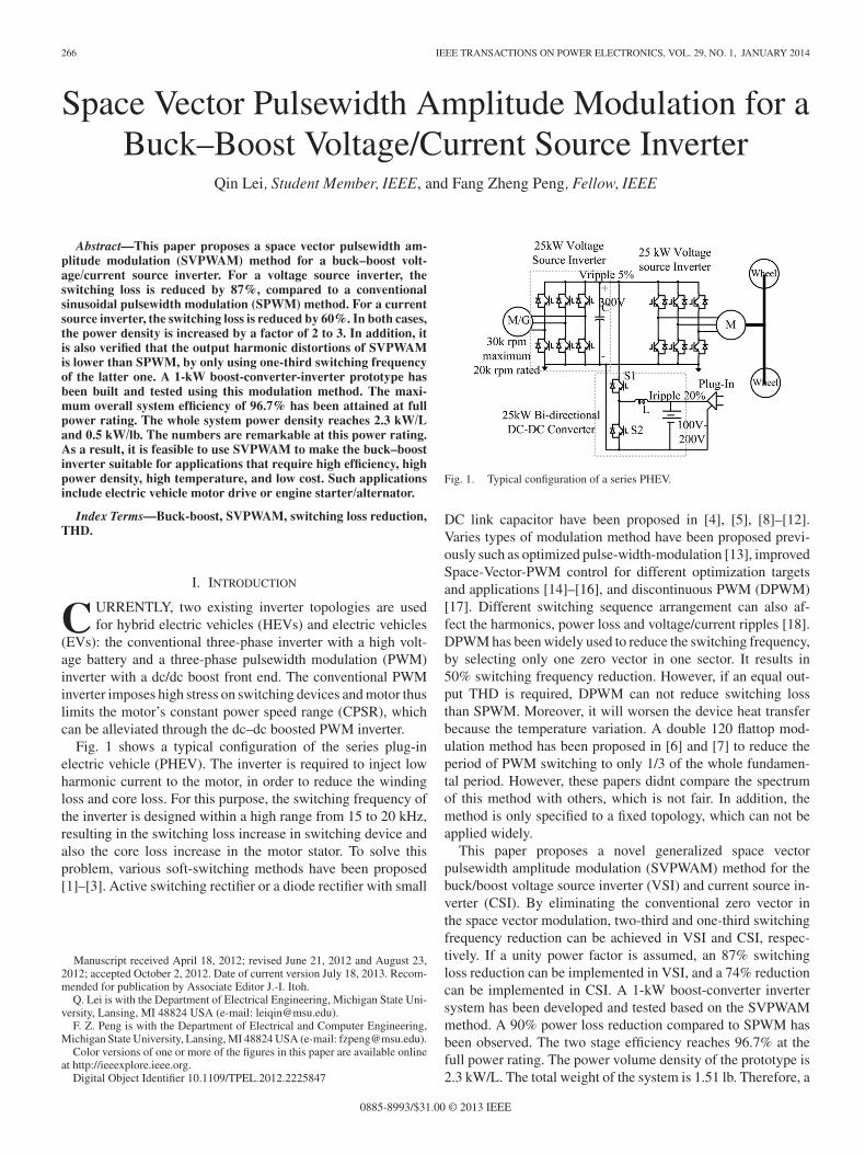
Fig. 1 shows a typical configuration of the series plug-inelectric vehicle (PHEV). The inverter is required to inject lowharmonic current to the motor, in order to reduce the windingloss and core loss. For this purpose, the switching frequency ofthe inverter is designed within a high range from 15 to 20 kHz,resulting in the switching loss increase in switching device andalso the core loss increase in the motor stator. To solve thisproblem, various soft-switching methods have been proposed[1]–[3]. Active switching rectifier or a diode rectifier with small
Manuscript received April 18, 2012; revised June 21, 2012 and August 23,2012; accepted October 2, 2012. Date of current version July 18, 2013. Recom-mended for publication by Associate Editor J.-I. Itoh.
Q. Lei is with the Department of Electrical Engineering, Michigan State Uni-versity, Lansing, MI 48824 USA (e-mail: [email protected]).
F. Z. Peng is with the Department of Electrical and Computer Engineering,Michigan State University, Lansing, MI 48824 USA (e-mail: [email protected]).
Color versions of one or more of the figures in this paper are available onlineat http://ieeexplore.ieee.org.
Digital Object Identifier 10.1109/TPEL.2012.2225847
Fig. 1. Typical configuration of a series PHEV.
DC link capacitor have been proposed in [4], [5], [8]–[12].Varies types of modulation method have been proposed previ-ously such as optimized pulse-width-modulation [13], improvedSpace-Vector-PWM control for different optimization targetsand applications [14]–[16], and discontinuous PWM (DPWM)[17]. Different switching sequence arrangement can also af-fect the harmonics, power loss and voltage/current ripples [18].DPWM has been widely used to reduce the switching frequency,by selecting only one zero vector in one sector. It results in50% switching frequency reduction. However, if an equal out-put THD is required, DPWM can not reduce switching lossthan SPWM. Moreover, it will worsen the device heat transferbecause the temperature variation. A double 120 flattop mod-ulation method has been proposed in [6] and [7] to reduce theperiod of PWM switching to only 1/3 of the whole fundamen-tal period. However, these papers didnt compare the spectrumof this method with others, which is not fair. In addition, themethod is only specified to a fixed topology, which can not beapplied widely.
This paper proposes a novel generalized space vectorpulsewidth amplitude modulation (SVPWAM) method for thebuck/boost voltage source inverter (VSI) and current source in-verter (CSI). By eliminating the conventional zero vector inthe space vector modulation, two-third and one-third switchingfrequency reduction can be achieved in VSI and CSI, respec-tively. If a unity power factor is assumed, an 87% switchingloss reduction can be implemented in VSI, and a 74% reductioncan be implemented in CSI. A 1-kW boost-converter invertersystem has been developed and tested based on the SVPWAMmethod. A 90% power loss reduction compared to SPWM hasbeen observed. The two stage efficiency reaches 96.7% at thefull power rating. The power volume density of the prototype is2.3 kW/L. The total weight of the system is 1.51 lb. Therefore, a
0885-8993/$31.00 © 2013 IEEE
LEI AND PENG: SPACE VECTOR PULSEWIDTH AMPLITUDE MODULATION FOR A BUCK–BOOST VOLTAGE/CURRENT SOURCE INVERTER 267
Fig. 2. SVPWAM for VSI.
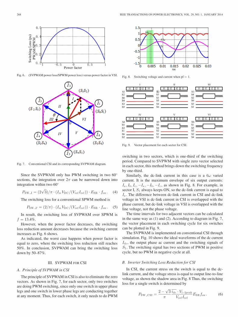
Fig. 3. DC-link voltage of SVPWAM in VSI.
high-efficiency, high-power density, high-temperature, and low-cost 1-kW inverter is achieved by using an SVPWAM method.
II. SVPWAM FOR VSI
A. Principle of SVPWAM Control in VSI
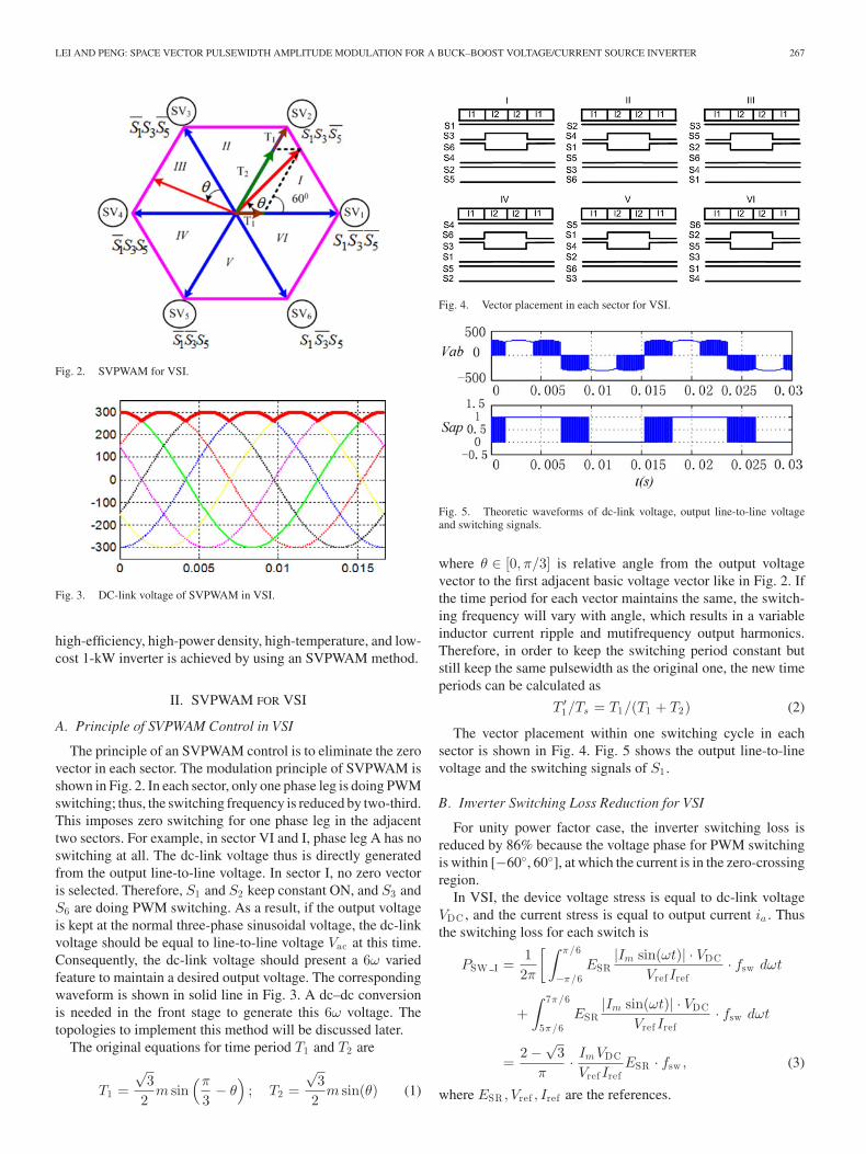
The principle of an SVPWAM control is to eliminate the zerovector in each sector. The modulation principle of SVPWAM isshown in Fig. 2. In each sector, only one phase leg is doing PWMswitching; thus, the switching frequency is reduced by two-third.This imposes zero switching for one phase leg in the adjacenttwo sectors. For example, in sector VI and I, phase leg A has noswitching at all. The dc-link voltage thus is directly generatedfrom the output line-to-line voltage. In sector I, no zero vectoris selected. Therefore, S1 and S2 keep constant ON, and S3 andS6 are doing PWM switching. As a result, if the output voltageis kept at the normal three-phase sinusoidal voltage, the dc-linkvoltage should be equal to line-to-line voltage Vac at this time.Consequently, the dc-link voltage should present a 6ω variedfeature to maintain a desired output voltage. The correspondingwaveform is shown in solid line in Fig. 3. A dc–dc conversionis needed in the front stage to generate this 6ω voltage. Thetopologies to implement this method will be discussed later.
The original equations for time period T1 and T2 are
T1 =√
32
m sin(π
3− θ
); T2 =
√3
2m sin(θ) (1)
Fig. 4. Vector placement in each sector for VSI.
Fig. 5. Theoretic waveforms of dc-link voltage, output line-to-line voltageand switching signals.
where θ ∈ [0, π/3] is relative angle from the output voltagevector to the first adjacent basic voltage vector like in Fig. 2. Ifthe time period for each vector maintains the same, the switch-ing frequency will vary with angle, which results in a variableinductor current ripple and mutifrequency output harmonics.Therefore, in order to keep the switching period constant butstill keep the same pulsewidth as the original one, the new timeperiods can be calculated as
T ′1/Ts = T1/(T1 + T2) (2)
The vector placement within one switching cycle in eachsector is shown in Fig. 4. Fig. 5 shows the output line-to-linevoltage and the switching signals of S1 .
B. Inverter Switching Loss Reduction for VSI
For unity power factor case, the inverter switching loss isreduced by 86% because the voltage phase for PWM switchingis within [−60◦, 60◦], at which the current is in the zero-crossingregion.
In VSI, the device voltage stress is equal to dc-link voltageVDC , and the current stress is equal to output current ia . Thusthe switching loss for each switch is
PSW I =12π
[ ∫ π/6
−π/6ESR
|Im sin(ωt)| · VDC
Vref Iref· fsw dωt
+∫ 7π/6
5π/6ESR
|Im sin(ωt)| · VDC
Vref Iref· fsw dωt
=2 −
√3
π· Im VDC
Vref IrefESR · fsw , (3)
where ESR , Vref , Iref are the references.
268 IEEE TRANSACTIONS ON POWER ELECTRONICS, VOL. 29, NO. 1, JANUARY 2014
Fig. 6. (SVPWAM power loss/SPWM power loss) versus power factor in VSI.
Fig. 7. Conventional CSI and its corresponding SVPWAM diagram.
Since the SVPWAM only has PWM switching in two 60◦
sections, the integration over 2π can be narrowed down intointegration within two 60◦
PSW I = (2√
3)/π · (Im VDC/(Vref Iref )) · ESR · fsw . (4)
The switching loss for a conventional SPWM method is
PSW I′ = (2/π) · (Im VDC/(Vref Iref )) · ESR · fsw . (5)
In result, the switching loss of SVPWAM over SPWM isf = 13.4%.
However, when the power factor decreases, the switchingloss reduction amount decreases because the switching currentincreases as Fig. 6 shows.
As indicated, the worst case happens when power factor isequal to zero, where the switching loss reduction still reaches50%. In conclusion, SVPWAM can bring the switching lossdown by 50–87%.
III. SVPWAM FOR CSI
A. Principle of SVPWAM in CSI
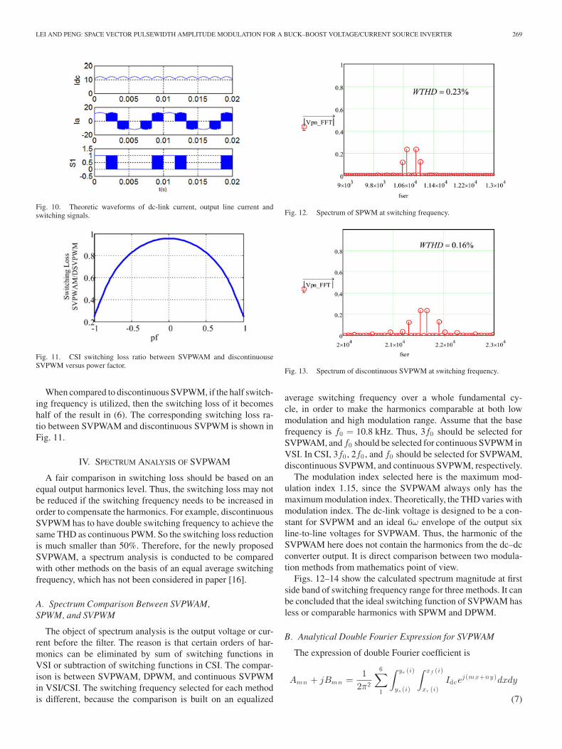
The principle of SVPWAM in CSI is also to eliminate the zerovectors. As shown in Fig. 7, for each sector, only two switchesare doing PWM switching, since only one switch in upper phaselegs and one switch in lower phase legs are conducting togetherat any moment. Thus, for each switch, it only needs to do PWM
Fig. 8. Switching voltage and current when pf = 1.
Fig. 9. Vector placement for each sector for CSI.
switching in two sectors, which is one-third of the switchingperiod. Compared to SVPWM with single zero vector selectedin each sector, this method brings down the switching frequencyby one-third.
Similarly, the dc-link current in this case is a 6ω variedcurrent. It is the maximum envelope of six output currents:Ia , Ib , Ic ,−Ia ,−Ib ,−Ic , as shown in Fig. 8. For example, insector I, S1 always keeps ON, so the dc-link current is equal toIa . The difference between dc-link current in CSI and dc-linkvoltage in VSI is dc-link current in CSI is overlapped with thephase current, but dc-link voltage in VSI is overlapped with theline voltage, not the phase voltage.
The time intervals for two adjacent vectors can be calculatedin the same way as (1) and (2). According to diagram in Fig. 7,the vector placement in each switching cycle for six switchescan be plotted in Fig. 9.
The SVPWAM is implemented on conventional CSI throughsimulation. Fig. 10 shows the ideal waveforms of the dc currentIdc , the output phase ac current and the switching signals ofS1 . The switching signal has two sections of PWM in positivecycle, but no PWM in negative cycle at all.
B. Inverter Switching Loss Reduction for CSI
In CSI, the current stress on the switch is equal to the dc-link current, and the voltage stress is equal to output line-to-linevoltage, as shown the shadow area in Fig. 8 Thus, the switchingloss for a single switch is determined by
PSW CSI =2 −
√3
π
idc · Vl−lpeak
Vref IrefESRfsw . (6)
LEI AND PENG: SPACE VECTOR PULSEWIDTH AMPLITUDE MODULATION FOR A BUCK–BOOST VOLTAGE/CURRENT SOURCE INVERTER 269
Fig. 10. Theoretic waveforms of dc-link current, output line current andswitching signals.
Fig. 11. CSI switching loss ratio between SVPWAM and discontinuouseSVPWM versus power factor.
When compared to discontinuous SVPWM, if the half switch-ing frequency is utilized, then the switching loss of it becomeshalf of the result in (6). The corresponding switching loss ra-tio between SVPWAM and discontinuous SVPWM is shown inFig. 11.
IV. SPECTRUM ANALYSIS OF SVPWAM
A fair comparison in switching loss should be based on anequal output harmonics level. Thus, the switching loss may notbe reduced if the switching frequency needs to be increased inorder to compensate the harmonics. For example, discontinuousSVPWM has to have double switching frequency to achieve thesame THD as continuous PWM. So the switching loss reductionis much smaller than 50%. Therefore, for the newly proposedSVPWAM, a spectrum analysis is conducted to be comparedwith other methods on the basis of an equal average switchingfrequency, which has not been considered in paper [16].
A. Spectrum Comparison Between SVPWAM,SPWM, and SVPWM
The object of spectrum analysis is the output voltage or cur-rent before the filter. The reason is that certain orders of har-monics can be eliminated by sum of switching functions inVSI or subtraction of switching functions in CSI. The compar-ison is between SVPWAM, DPWM, and continuous SVPWMin VSI/CSI. The switching frequency selected for each methodis different, because the comparison is built on an equalized
Fig. 12. Spectrum of SPWM at switching frequency.
Fig. 13. Spectrum of discontinuous SVPWM at switching frequency.
average switching frequency over a whole fundamental cy-cle, in order to make the harmonics comparable at both lowmodulation and high modulation range. Assume that the basefrequency is f0 = 10.8 kHz. Thus, 3f0 should be selected forSVPWAM, and f0 should be selected for continuous SVPWM inVSI. In CSI, 3f0 , 2f0 , and f0 should be selected for SVPWAM,discontinuous SVPWM, and continuous SVPWM, respectively.
The modulation index selected here is the maximum mod-ulation index 1.15, since the SVPWAM always only has themaximum modulation index. Theoretically, the THD varies withmodulation index. The dc-link voltage is designed to be a con-stant for SVPWM and an ideal 6ω envelope of the output sixline-to-line voltages for SVPWAM. Thus, the harmonic of theSVPWAM here does not contain the harmonics from the dc–dcconverter output. It is direct comparison between two modula-tion methods from mathematics point of view.
Figs. 12–14 show the calculated spectrum magnitude at firstside band of switching frequency range for three methods. It canbe concluded that the ideal switching function of SVPWAM hasless or comparable harmonics with SPWM and DPWM.
B. Analytical Double Fourier Expression for SVPWAM
The expression of double Fourier coefficient is
Amn + jBmn =1
2π2
6∑1
∫ ye (i)
ys (i)
∫ xf (i)
xr (i)Idce
j (mx+ny )dxdy
(7)
270 IEEE TRANSACTIONS ON POWER ELECTRONICS, VOL. 29, NO. 1, JANUARY 2014
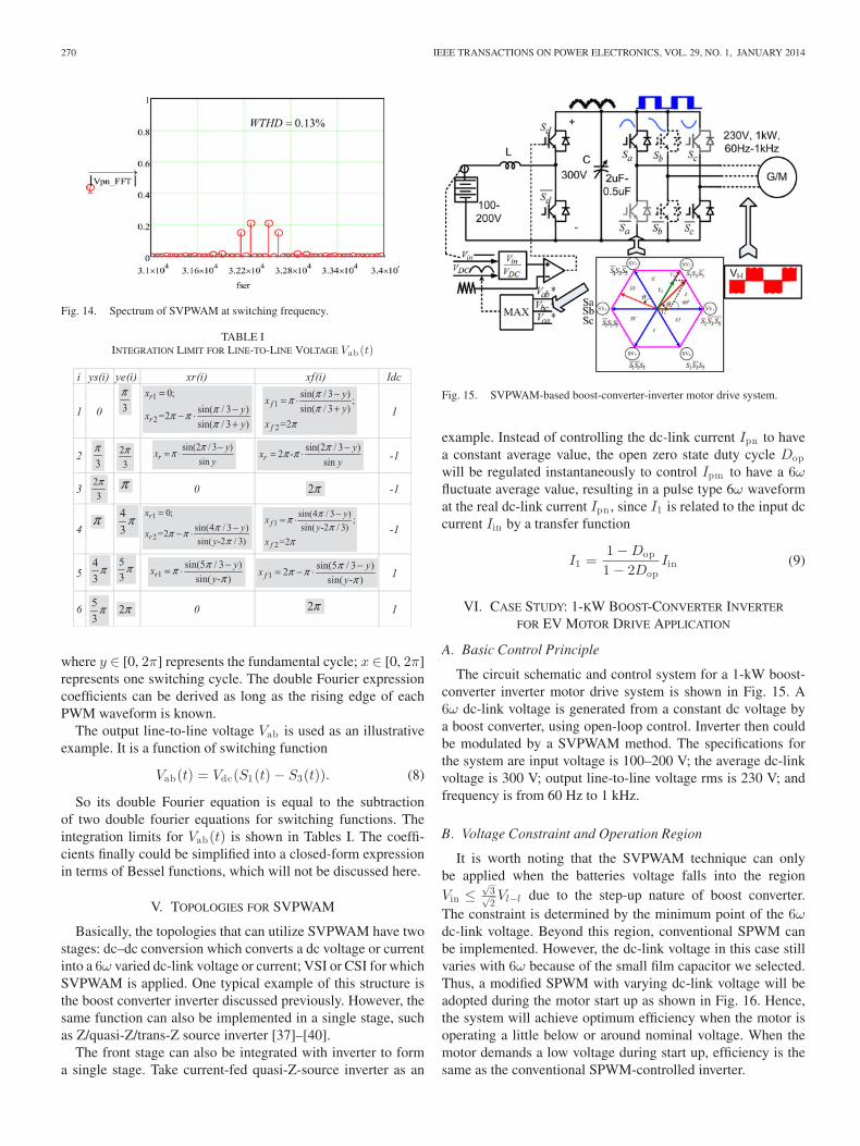
Fig. 14. Spectrum of SVPWAM at switching frequency.
TABLE IINTEGRATION LIMIT FOR LINE-TO-LINE VOLTAGE Vab (t)
i ys(i) ye(i) xr(i) xf(i) Idc
1 0 1
2 -1
3 0 -1
4 -1
5 1
6 0 1
3
π
3
π 2
3
π
2
3
π π
π 4
3π
4
3π
5
3π
5
3π 2π
sin(2 / 3 )
sinry
xy
ππ −= ⋅
1sin(5 / 3 )
sin( - )ry
xy
πππ−= ⋅ 1
sin(5 / 3 )2
sin( - )fy
xy
ππ ππ−= − ⋅
2π
1
2
0;
sin( / 3 )=2
sin( / 3 )
r
r
x
yx
y
ππ ππ
=−− ⋅+
1
2
sin( / 3 );
sin( / 3 )
=2
f
f
yx
y
x
πππ
π
−= ⋅+
sin(2 / 3 )2 -
sinry
xy
ππ π −= ⋅
1
2
0;
sin(4 / 3 )=2
sin( -2 / 3)
r
r
x
yx
y
ππ ππ
=−− ⋅
1
2
sin(4 / 3 );
sin( -2 / 3)
=2
f
f
yx
y
x
πππ
π
−= ⋅
2π
where y ∈ [0, 2π] represents the fundamental cycle; x ∈ [0, 2π]represents one switching cycle. The double Fourier expressioncoefficients can be derived as long as the rising edge of eachPWM waveform is known.
The output line-to-line voltage Vab is used as an illustrativeexample. It is a function of switching function
Vab(t) = Vdc(S1(t) − S3(t)). (8)
So its double Fourier equation is equal to the subtractionof two double fourier equations for switching functions. Theintegration limits for Vab(t) is shown in Tables I. The coeffi-cients finally could be simplified into a closed-form expressionin terms of Bessel functions, which will not be discussed here.
V. TOPOLOGIES FOR SVPWAM
Basically, the topologies that can utilize SVPWAM have twostages: dc–dc conversion which converts a dc voltage or currentinto a 6ω varied dc-link voltage or current; VSI or CSI for whichSVPWAM is applied. One typical example of this structure isthe boost converter inverter discussed previously. However, thesame function can also be implemented in a single stage, suchas Z/quasi-Z/trans-Z source inverter [37]–[40].
The front stage can also be integrated with inverter to forma single stage. Take current-fed quasi-Z-source inverter as an
Fig. 15. SVPWAM-based boost-converter-inverter motor drive system.
example. Instead of controlling the dc-link current Ipn to havea constant average value, the open zero state duty cycle Dopwill be regulated instantaneously to control Ipm to have a 6ωfluctuate average value, resulting in a pulse type 6ω waveformat the real dc-link current Ipn , since I1 is related to the input dccurrent Iin by a transfer function
I1 =1 − Dop
1 − 2DopIin (9)
VI. CASE STUDY: 1-KW BOOST-CONVERTER INVERTER
FOR EV MOTOR DRIVE APPLICATION
A. Basic Control Principle
The circuit schematic and control system for a 1-kW boost-converter inverter motor drive system is shown in Fig. 15. A6ω dc-link voltage is generated from a constant dc voltage bya boost converter, using open-loop control. Inverter then couldbe modulated by a SVPWAM method. The specifications forthe system are input voltage is 100–200 V; the average dc-linkvoltage is 300 V; output line-to-line voltage rms is 230 V; andfrequency is from 60 Hz to 1 kHz.
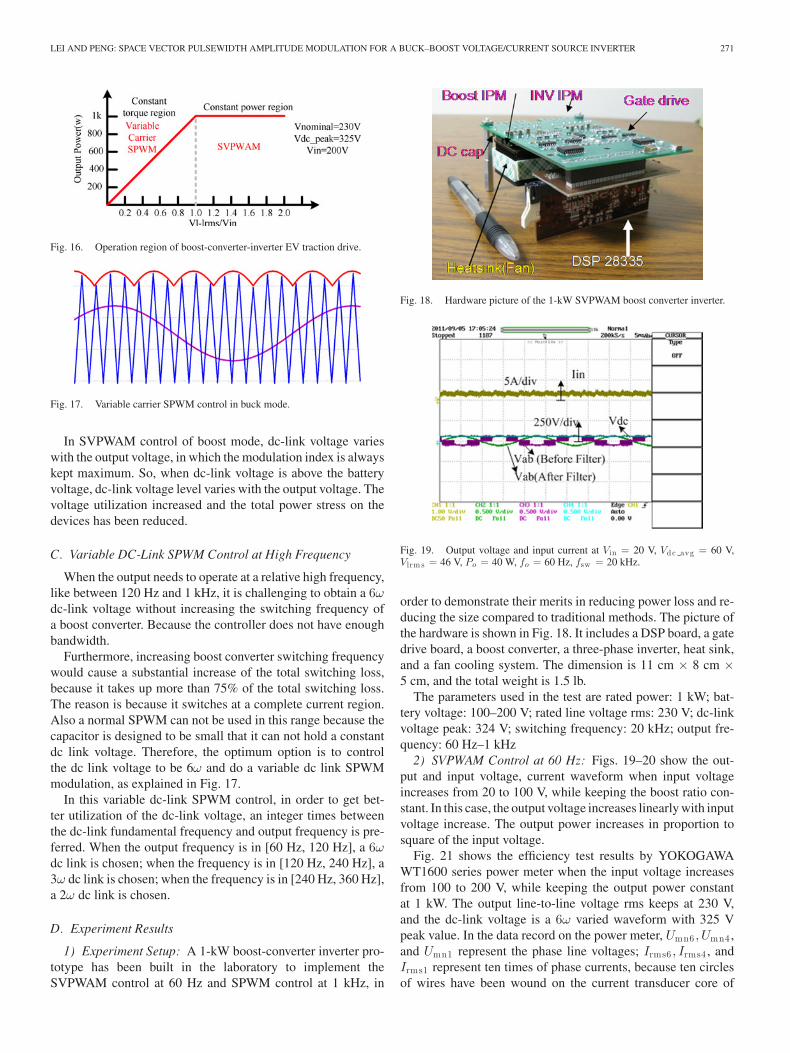
B. Voltage Constraint and Operation Region
It is worth noting that the SVPWAM technique can onlybe applied when the batteries voltage falls into the regionVin ≤
√3√2Vl−l due to the step-up nature of boost converter.
The constraint is determined by the minimum point of the 6ωdc-link voltage. Beyond this region, conventional SPWM canbe implemented. However, the dc-link voltage in this case stillvaries with 6ω because of the small film capacitor we selected.Thus, a modified SPWM with varying dc-link voltage will beadopted during the motor start up as shown in Fig. 16. Hence,the system will achieve optimum efficiency when the motor isoperating a little below or around nominal voltage. When themotor demands a low voltage during start up, efficiency is thesame as the conventional SPWM-controlled inverter.
LEI AND PENG: SPACE VECTOR PULSEWIDTH AMPLITUDE MODULATION FOR A BUCK–BOOST VOLTAGE/CURRENT SOURCE INVERTER 271
Fig. 16. Operation region of boost-converter-inverter EV traction drive.
Fig. 17. Variable carrier SPWM control in buck mode.
In SVPWAM control of boost mode, dc-link voltage varieswith the output voltage, in which the modulation index is alwayskept maximum. So, when dc-link voltage is above the batteryvoltage, dc-link voltage level varies with the output voltage. Thevoltage utilization increased and the total power stress on thedevices has been reduced.
C. Variable DC-Link SPWM Control at High Frequency
When the output needs to operate at a relative high frequency,like between 120 Hz and 1 kHz, it is challenging to obtain a 6ωdc-link voltage without increasing the switching frequency ofa boost converter. Because the controller does not have enoughbandwidth.
Furthermore, increasing boost converter switching frequencywould cause a substantial increase of the total switching loss,because it takes up more than 75% of the total switching loss.The reason is because it switches at a complete current region.Also a normal SPWM can not be used in this range because thecapacitor is designed to be small that it can not hold a constantdc link voltage. Therefore, the optimum option is to controlthe dc link voltage to be 6ω and do a variable dc link SPWMmodulation, as explained in Fig. 17.
In this variable dc-link SPWM control, in order to get bet-ter utilization of the dc-link voltage, an integer times betweenthe dc-link fundamental frequency and output frequency is pre-ferred. When the output frequency is in [60 Hz, 120 Hz], a 6ωdc link is chosen; when the frequency is in [120 Hz, 240 Hz], a3ω dc link is chosen; when the frequency is in [240 Hz, 360 Hz],a 2ω dc link is chosen.
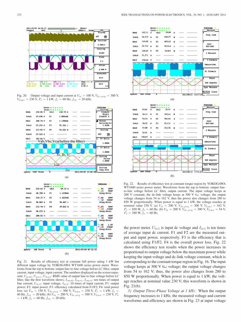
D. Experiment Results
1) Experiment Setup: A 1-kW boost-converter inverter pro-totype has been built in the laboratory to implement theSVPWAM control at 60 Hz and SPWM control at 1 kHz, in
Fig. 18. Hardware picture of the 1-kW SVPWAM boost converter inverter.
Fig. 19. Output voltage and input current at Vin = 20 V, Vdc avg = 60 V,Vlrm s = 46 V, Po = 40 W, fo = 60 Hz, fsw = 20 kHz.
order to demonstrate their merits in reducing power loss and re-ducing the size compared to traditional methods. The picture ofthe hardware is shown in Fig. 18. It includes a DSP board, a gatedrive board, a boost converter, a three-phase inverter, heat sink,and a fan cooling system. The dimension is 11 cm × 8 cm ×5 cm, and the total weight is 1.5 lb.
The parameters used in the test are rated power: 1 kW; bat-tery voltage: 100–200 V; rated line voltage rms: 230 V; dc-linkvoltage peak: 324 V; switching frequency: 20 kHz; output fre-quency: 60 Hz–1 kHz
2) SVPWAM Control at 60 Hz: Figs. 19–20 show the out-put and input voltage, current waveform when input voltageincreases from 20 to 100 V, while keeping the boost ratio con-stant. In this case, the output voltage increases linearly with inputvoltage increase. The output power increases in proportion tosquare of the input voltage.
Fig. 21 shows the efficiency test results by YOKOGAWAWT1600 series power meter when the input voltage increasesfrom 100 to 200 V, while keeping the output power constantat 1 kW. The output line-to-line voltage rms keeps at 230 V,and the dc-link voltage is a 6ω varied waveform with 325 Vpeak value. In the data record on the power meter, Umn6 , Umn4 ,and Umn1 represent the phase line voltages; Irms6 , Irms4 , andIrms1 represent ten times of phase currents, because ten circlesof wires have been wound on the current transducer core of
272 IEEE TRANSACTIONS ON POWER ELECTRONICS, VOL. 29, NO. 1, JANUARY 2014
Fig. 20. Output voltage and input current at Vin = 100 V, Vdc avg = 300 V,Vlrm s = 230 V, Po = 1 kW, fo = 60 Hz, fsw = 20 kHz.
Fig. 21. Results of efficiency test at constant full power rating 1 kW butdifferent input voltage by YOKOGAWA WT1600 series power meter. Wave-forms from the top to bottom: output line-to-line voltage before LC filter, outputcurrent, input voltage, input current. The numbers displayed on the screen repre-sent: Um n6 , Um n1 , Um n4 : RMS value of output line-to-line voltage before LCfilter, like the first waveform shows; Irm s6 , Irm s1 , Irm s4 : ten times of outputline current; Udc2 : input voltage; Idc2 : 10 times of input current; F1: outputpower; F2: input power; F3: efficiency calculated from F1/F2; F4: total powerloss: (a) Vin = 150 V, Vdc avg = 300 V, Vlrm s = 230 V, Po = 1 kW, fo =60 Hz, fsw = 20 kHz; (b) Vin = 200 V, Vdc avg = 300 V, Vlrm s = 230 V, Po
= 1 kW, fo = 60 Hz, fsw = 20 kHz.
Fig. 22. Results of efficiency test at constant torque region by YOKOGAWAWT1600 series power meter. Waveforms from the top to bottom: output line-to-line voltage before LC filter, output current. The input voltage keeps at200 V constant; the dc-link voltage keeps at 300 V 6ω voltage; the outputvoltage changes from 54 to 162 V, thus the power also changes from 280 to850 W proportionally. When power is equal to 1 kW, the voltage reaches atnominal value 230 V. (a) Vin = 200 V, Vdc avg = 300 V, Vlrm s = 162 V,Po = 850 W, fo = 60 Hz. (b) Vin = 200 V, Vdc avg = 300 V, Vlrm s = 54 V,Po = 280 W, fo = 60 Hz.
the power meter. Udc2 is input dc voltage and Idc2 is ten timesof average input dc current. F1 and F2 are the measured out-put and input power, respectively. F3 is the efficiency that iscalculated using F1/F2. F4 is the overall power loss. Fig. 22shows the efficiency test results when the power increases inproportional to output voltage below the maximum power whilekeeping the input voltage and dc-link voltage constant, which iscorresponding to the constant torque region in Fig. 16. The inputvoltage keeps at 300 V 6ω voltage; the output voltage changesfrom 54 to 162 V; thus, the power also changes from 280 to850 W proportionally. When power is equal to 1 kW, the volt-age reaches at nominal value 230 V; this waveform is shown inFig. 21(b).
3) Output Three-Phase Voltage at 1 kHz: When the outputfrequency increases to 1 kHz, the measured voltage and currentwaveforms and efficiency are shown in Fig. 23 at input voltage
LEI AND PENG: SPACE VECTOR PULSEWIDTH AMPLITUDE MODULATION FOR A BUCK–BOOST VOLTAGE/CURRENT SOURCE INVERTER 273
Fig. 23. The efficiency test at Vin = 150 V at fo = 1 kHz: from top to bottom:output line voltage, output current, and input current.
Fig. 24. Measured overall efficiency when input voltage changes from 100to 200 V at 1-kW power rating corresponding to Fig. 23 (fo = 60 Hz, fsw =20 kHz, Vdc p eak = 325 V, V ol-lrm s = 230 V).
150 V. The efficiency is around 84% for both cases, lower than60 Hz case.
E. Overall Efficiency and Power Loss Comparison BetweenSVPWAM and SPWM
Fig. 24 shows the measured efficiency when the input voltageincreases from 100 to 200 V, all at 1-kW power rating. The over-all efficiency increases as the input voltage increases, becausethe efficiency of a boost converter increases when the input volt-age increases. The maximum efficiency at 1 kW reaches 96.7%at input voltage 200 V. Fig. 25 shows the joined results of theconstant torque region and constant power region in Fig. 16.It can be seen that the maximum efficiency at constant torqueregion happens at its maximum output voltage where the volt-age gain is equal to 1, and the maximum efficiency at constantpower region power happens at its minimum voltage gain point,which is also equal to 1. At constant power region, the efficiencydecreases as the voltage increases while keeping the power con-stant.
Fig. 26(a) and (b) shows the power loss estimation (from theloss model mentioned before) of the inverter when the power
Fig. 25. Efficiency versus voltage gain results corresponding to Fig. 19.
Fig. 26. Comparison between inverter power losses in the condition that dc-link voltage changes from 0 to full rating at 300 V: (a) SVPWAM, (b) SPWM.
increases from 0 to full rating under two methods. Since theresearch target is only inverter, the test condition is based onvarying the output power by changing output voltage from 0to 230 V. It is observed that in the SVPWAM method, conduc-tion loss accounts for 80% of the total power loss, but in theSPWM method, switching loss is higher than conduction loss.The switching loss is reduced from 10 to 1.4 W from SPWMto SVPWAM. An estimated 87% switching loss reduction hasbeen achieved.
VII. CONCLUSION
The SVPWAM control method preserves the following ad-vantages compared to traditional SPWM and SVPWM method.
1) The switching power loss is reduced by 90% comparedwith the conventional SPWM inverter system.

274 IEEE TRANSACTIONS ON POWER ELECTRONICS, VOL. 29, NO. 1, JANUARY 2014
2) The power density is increased by a factor of 2 becauseof reduced dc capacitor (from 40 to 6 μF) and small heatsink is needed.
3) The cost is reduced by 30% because of reduced passives,heat sink, and semiconductor stress.
A high-efficiency, high-power density, high-temperature, andlow-cost 1-kW inverter engine drive system has been developedand tested. The effectiveness of the proposed method in reduc-tion of power losses has been validated by the experimentalresults that were obtained from the laboratory scale prototype.
REFERENCES
[1] D. M. Divan and G. Skibinski, “Zero-switching-loss inverters for high-power applications,” IEEE Trans. Ind. Appl., vol. 25, no. 4, pp. 634–643,Jul./Aug. 1989.
[2] W. McMurray, “Resonant snubbers with auxiliary switches,” IEEE Trans.Ind. Appl., vol. 29, no. 2, pp. 355–362, Mar./Apr. 1993.
[3] J.-S. Lai, R. W. Young, Sr., G. W. Ott, Jr., J. W. McKeever, and F. Z. Peng,“A delta-configured auxiliary resonant snubber inverter,” IEEE Trans. Ind.Appl., vol. 32, no. 3, pp. 518–525, May/Jun. 1996.
[4] J. S. Kim and S. K. Sul, “New control scheme for ac-dc-ac converterwithout dc link electrolytic capacitor,” in Proc. 24th Annu. IEEE PowerElectron. Spec. Conf., Jun. 1993, pp. 300–306.
[5] K. Rigbers, S. Thomas, U. Boke, and R. W. De Doncker, “Behavior andloss modeling of a three-phase resonant pole inverter operating with 120Adouble flattop modulation,” in Proc. 41st IAS Annu. Meeting IEEE Ind.Appl. Conf., Oct. 8–12, 2006, vol. 4, pp. 1694–1701.
[6] J. Shen, K Rigbers, C. P. Dick, and R. W. De Doncker, “A dynamic boostconverter input stage for a double 120◦ flattop modulation based three-phase inverter,” in Proc. IEEE Ind. Appl. Soc. Annu. Meeting, Oct. 5–9,2008, pp. 1–7.
[7] H. Fujita, “A three-phase voltage-source solar power conditioner usinga single-phase PWM control method,” in Proc. IEEE Energy Convers.Congr. Expo., 2009, pp. 3748–3754.
[8] H. Haga, K. Nishiya, S. Kondo, and K. Ohishi, “High power factor controlof electrolytic capacitor less current-fed single-phase to three-phase powerconverter,” in Proc. Int. Power Electron. Conf., Jun. 21–24, 2010, pp. 443–448.
[9] X. Chen and M. Kazerani, “Space vector modulation control of an ac-dc-acconverter with a front-end diode rectifier and reduced dc-link capacitor,”IEEE Trans. Power Electron., vol. 21, no. 5, pp. 1470–1478, Sep. 2006.
[10] M. Hinkkanen and J. Luomi, “Induction motor drives equipped withdiode rectifier and small dc-link capacitance,” IEEE Trans. Ind. Electron.,vol. 55, no. 1, pp. 312–320, Jan. 2008.
[11] J. Jung, S. Lim, and K. Nam, “A feedback linearizing control scheme fora PWM converter-inverter having a very small dc-link capacitor,” IEEETrans. Ind. Appl., vol. 35, no. 5, pp. 1124–1131, Sep./Oct. 1999.
[12] L. Malesani, L. Rossetto, P. Tenti, and P. Tomasin, “AC/DC/AC PWMconverter with reduced energy storage in the dc link,” IEEE Trans. Ind.Appl., vol. 31, no. 2, pp. 287–292, Mar./Apr. 1995.
[13] T. Bruckner and D. G. Holmes, “Optimal pulse-width modulation forthree-level inverters,” IEEE Trans. Power Electron., vol. 20, no. 1, pp. 82–89, Jan. 2005.
[14] F. Blaabjerg, S. Freysson, H.-H. Hansen, and S. Hansen, “A new op-timized space-vector modulation strategy for a component-minimizedvoltage source inverter,” IEEE Trans. Power Electron., vol. 12, no. 4,pp. 704–714, Jul. 1997.
[15] M. M. Bech, F. Blaabjerg, and J. K. Pedersen, “Random modulation tech-niques with fixed switching frequency for three-phase power converters,”IEEE Trans. Power Electron., vol. 15, no. 4, pp. 753–761, Jul. 2000.
[16] F. Blaabjerg, D. O. Neacsu, and J. K. Pedersen, “Adaptive SVM to com-pensate dc-link voltage ripple for four-switch three-phase voltage-sourceinverters,” IEEE Trans. Power Electron., vol. 14, no. 4, pp. 743–752, Jul.1999.
[17] L. Asiminoaei, P. Rodriguez, and F. Blaabjerg, “Application of discon-tinuous PWM modulation in active power filters,” IEEE Trans. PowerElectron., vol. 23, no. 4, pp. 1692–1706, Jul. 2008.
[18] B. P. McGrath, D. G. Holmes, and T. Lipo, “Optimized space vectorswitching sequences for multilevel inverters,” IEEE Trans. Power Elec-tron., vol. 18, no. 6, pp. 1293–1301, Nov. 2003.
[19] R. Zhang, V. H. Prasad, D. Boroyevich, and F. C. Lee, “Three-dimensionalspace vector modulation for four-leg voltage-source converters,” IEEETrans. Power Electron., vol. 17, no. 3, pp. 314–326, May 2002.
[20] R. Burgos, R. Lai, Y. Pei, F. Wang, D. Boroyevich, and J. Pou, “Spacevector modulator for vienna-type rectifiersbased on the equivalencebetweentwo- and three-level converters: A carrier-based implementation,”IEEE Trans. Power Electron., vol. 23, no. 4, pp. 1888–1898, Jul. 2008.
[21] P. C. Loh, D. M. Vilathgamuwa, Y. S. Lai, G. T. Chua, and Y. Li, “Pulse-width modulation of Z-source inverters,” IEEE Trans. Power Electron.,vol. 20, no. 6, pp. 1346–1355, Nov. 2005.
[22] F. Z. Peng, “Z-source inverter,” IEEE Trans. Ind. Appl., vol. 39, no. 2,pp. 504–510, Mar./Apr. 2003.
Qin Lei (S’09) received the B. S. degree in electri-cal engineering from Huazhong University of Scienceand Technology, Wuhan, China, in 2006, and the Ph.Ddegree in electrical engineering from Michigan StateUniversity, Ann Arbor, MI, USA, in Sep. 2012.
After graduation, she joined General ElectricGlobal Research Center, Niskayuna, where she is anElectric Engineer now. Her research interests includehigh power converter control, HEV/EV motor drive,microgrid, and Z-source inverter.
Fang Zheng Peng (M’92-SM’96-F’04) received theB.S. degree in electrical engineering from WuhanUniversity, China, in 1983, and the M.S. and Ph.D.degrees, both in electrical engineering, from NagaokaUniversity of Technology, Japan, in 1987 and 1990,respectively.
From 1990 to 1992, he was a Research Scientistwith Toyo Electric Manufacturing Co., Ltd., where hewas engaged in research and development of activepower filters, utility applications, and motor drives.From 1992 to 1994, he worked with Tokyo Institute
of Technology as a Research Assistant Professor, where he initiated a multilevelinverter program and a speed-sensorless vector control project. From 1994 to2000, he worked for Oak Ridge National Laboratory (ORNL), first as a ResearchAssistant Professor at the University of Tennessee, Knoxville from 1994 to 1997and was then a Staff Member, Lead (principal) Scientist of the Power Electronicsand Electric Machinery Research Center at ORNL from 1997 to 2000. In 2000,he joined Michigan State University as an Associate Professor and he is now aFull Professor of the Department of Electrical and Computer Engineering. Heholds over 10 patents and two of them have been used extensively in industry.
Dr. Peng received many awards including the 1991 First Prize Paper Awardin IEEE TRANSACTIONS ON INDUSTRY APPLICATIONS and the 1990Best Paper Award in the Transactions of the IEE of Japan, the Promotion Awardof Electrical Academy. He has served the IEEE Power Electronics Society inmany including as Awards Chair, Chair of Technical Committee, an AssociateEditor for the Transactions, Region 1-6 Liaison and AdCom Member-at-Large.He was an IEEE/IAS Distinguished Lecturer for the 2010–2011 term.
Related Documents