Top Banner
Survey on Photonics and Novel Op6cal Materials Minghao Qi Purdue University DLA 2011 SLAC Na=onal Accelerator Laboratory September 15, 2011
36

SurveyonPhotonicsandNovel Op6cal’Materials’ · SurveyonPhotonicsandNovel Op6cal’Materials’ Minghao(Qi(Purdue(University(DLA2011 SLAC(Naonal(Accelerator(Laboratory(September15,2011

Sep 12, 2018

Download

Documents

hoangthu
Welcome message from author
This document is posted to help you gain knowledge. Please leave a comment to let me know what you think about it! Share it to your friends and learn new things together.
Transcript
Page 1: SurveyonPhotonicsandNovel Op6cal’Materials’ · SurveyonPhotonicsandNovel Op6cal’Materials’ Minghao(Qi(Purdue(University(DLA2011 SLAC(Naonal(Accelerator(Laboratory(September15,2011

Survey  on  Photonics  and  Novel  Op6cal  Materials  

Minghao  Qi  Purdue  University  

DLA  2011  

SLAC  Na=onal  Accelerator  Laboratory  

September  15,  2011  

Page 2: SurveyonPhotonicsandNovel Op6cal’Materials’ · SurveyonPhotonicsandNovel Op6cal’Materials’ Minghao(Qi(Purdue(University(DLA2011 SLAC(Naonal(Accelerator(Laboratory(September15,2011

Photonics  and  Novel  Op=cal  Materials  

•  Outline  –  On-­‐chip  hollow  TM  structures  –  On-­‐chip  accelerator  based  on  Omniguide  waveguides  

–  Fiber  to  waveguide  couplers,  power  spliJers  – Materials  and  Damage    

–  New  fabrica=on  approach  to  Woodpile  3D  photonic  crystals  

Page 3: SurveyonPhotonicsandNovel Op6cal’Materials’ · SurveyonPhotonicsandNovel Op6cal’Materials’ Minghao(Qi(Purdue(University(DLA2011 SLAC(Naonal(Accelerator(Laboratory(September15,2011

On-­‐Chip  TM-­‐Mode  Waveguides  •  Must  be  hollow  •  Need  to  have  a  phase  speed  matched  with  the  speed  of  the  bunch  – At  high  par=cle  energy,  phase  velocity  must  match  c  

•  Prefer  to  be  strongly  confined  – Higher  gradient  

•  Omniguide  fiber,  PhC  fibers,  3D  photonic  crystals  – Tunable  to  tolerate  fabrica=on  varia=ons  – Low  nonlinearity?  

Page 4: SurveyonPhotonicsandNovel Op6cal’Materials’ · SurveyonPhotonicsandNovel Op6cal’Materials’ Minghao(Qi(Purdue(University(DLA2011 SLAC(Naonal(Accelerator(Laboratory(September15,2011

Omni-­‐Guide  Fibers  

•  Direct  analogy  with  hollow  metallic  waveguides  –  Cylindrical  symmetry  may  facilitate  TM  modes  

•  Also  called  Bragg  Fibers  

•  We  need  to  bring  them  onto  chips  

S.  G.  Johnson,  et  al,  Op=cs  Express,  9,  748-­‐779,  (2001)  

Page 5: SurveyonPhotonicsandNovel Op6cal’Materials’ · SurveyonPhotonicsandNovel Op6cal’Materials’ Minghao(Qi(Purdue(University(DLA2011 SLAC(Naonal(Accelerator(Laboratory(September15,2011

Engineering  Op=ons  

•  Indices:  Red:  2.8,  blue:  1.5  •  TM  band  gap  intersects  light  line.  

T.  D.  Engeness,  et  al,  Op=cs  Express,  10,    1175-­‐1196,  (2003)  

Page 6: SurveyonPhotonicsandNovel Op6cal’Materials’ · SurveyonPhotonicsandNovel Op6cal’Materials’ Minghao(Qi(Purdue(University(DLA2011 SLAC(Naonal(Accelerator(Laboratory(September15,2011

Hybrid  Modes  can  Intersect  Light  Line  

T.  D.  Engeness,  et  al,  Op=cs  Express,  10,    1175-­‐1196,  (2003)  

Page 7: SurveyonPhotonicsandNovel Op6cal’Materials’ · SurveyonPhotonicsandNovel Op6cal’Materials’ Minghao(Qi(Purdue(University(DLA2011 SLAC(Naonal(Accelerator(Laboratory(September15,2011

Higher  Order  TM  Modes  Could  Intersect  with  Light  Line  

G.  Ouyang,  et  al,  Op=cs  Express,  10,    899-­‐908,  (2002)  

Page 8: SurveyonPhotonicsandNovel Op6cal’Materials’ · SurveyonPhotonicsandNovel Op6cal’Materials’ Minghao(Qi(Purdue(University(DLA2011 SLAC(Naonal(Accelerator(Laboratory(September15,2011

Proposal  of  an  On-­‐Chip  Accelerator  

Electron  bunches  

Beam  posi=on  sensor  

Accelera=on  module  

Focusing  module  

Laser  input  fiber,  l1  

Laser  input  fiber,  l2  

Si

W SiO2

•  Inner  diameters  can  be  different  and  controlled  

Page 9: SurveyonPhotonicsandNovel Op6cal’Materials’ · SurveyonPhotonicsandNovel Op6cal’Materials’ Minghao(Qi(Purdue(University(DLA2011 SLAC(Naonal(Accelerator(Laboratory(September15,2011

How  to  Fabricate  It?  

•  Standard  CMOS  process  except  wafer  bonding  •  Does  not  require  deep  submicron  technology  

•  Can  control  the  inner  diameter  

Si W

Si W

SiN SiN

Page 10: SurveyonPhotonicsandNovel Op6cal’Materials’ · SurveyonPhotonicsandNovel Op6cal’Materials’ Minghao(Qi(Purdue(University(DLA2011 SLAC(Naonal(Accelerator(Laboratory(September15,2011

Oxida=on  to  Achieve  Circular  Shape  

•  Require  aligned  wafer  bonding  (but  just  once)  •  Tungsten  as  quadruple-­‐poles  to  withstand  high  temperature.  

SiN SiN SiN SiN

Si

W

Si

W

Page 11: SurveyonPhotonicsandNovel Op6cal’Materials’ · SurveyonPhotonicsandNovel Op6cal’Materials’ Minghao(Qi(Purdue(University(DLA2011 SLAC(Naonal(Accelerator(Laboratory(September15,2011

Chop  the  hollow  waveguide  to  right  length  

•  Right  module  length  for  accelera=on  and  focusing  •  Short  enough  for  atomic  layer  deposi=on  to  work  

Page 12: SurveyonPhotonicsandNovel Op6cal’Materials’ · SurveyonPhotonicsandNovel Op6cal’Materials’ Minghao(Qi(Purdue(University(DLA2011 SLAC(Naonal(Accelerator(Laboratory(September15,2011

ALD  to  coat  the  inner  Bragg  layers  

•  Atomic  Layer  Deposi=on  is  extremely  uniform  

Short distance to waveguide terminals

Page 13: SurveyonPhotonicsandNovel Op6cal’Materials’ · SurveyonPhotonicsandNovel Op6cal’Materials’ Minghao(Qi(Purdue(University(DLA2011 SLAC(Naonal(Accelerator(Laboratory(September15,2011

Previous  Demonstra=on  on  Chip  

T.  C.  Shen,  et  al,  Journal  of  Lightwave  Technology,  28,  1714,  (2011)  

G.  R.  Hadley,  et  al,  Op=cs  LeJers,  29,    809,  (2004)  

•  Not  using  ALD  •  With  deposi=on  of  Si  followed  by  oxida=on  of  Si  
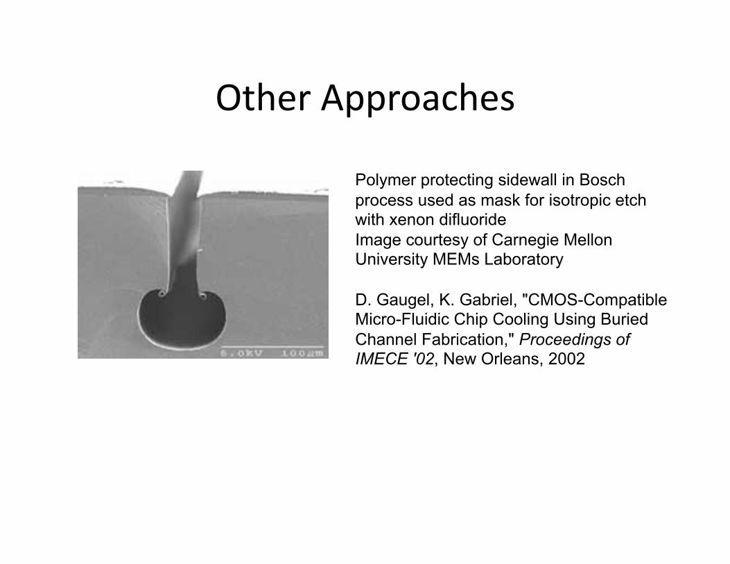
Page 14: SurveyonPhotonicsandNovel Op6cal’Materials’ · SurveyonPhotonicsandNovel Op6cal’Materials’ Minghao(Qi(Purdue(University(DLA2011 SLAC(Naonal(Accelerator(Laboratory(September15,2011

Other  Approaches  

Polymer protecting sidewall in Bosch process used as mask for isotropic etch with xenon difluoride Image courtesy of Carnegie Mellon University MEMs Laboratory

D. Gaugel, K. Gabriel, "CMOS-Compatible Micro-Fluidic Chip Cooling Using Buried Channel Fabrication," Proceedings of IMECE '02, New Orleans, 2002

Page 15: SurveyonPhotonicsandNovel Op6cal’Materials’ · SurveyonPhotonicsandNovel Op6cal’Materials’ Minghao(Qi(Purdue(University(DLA2011 SLAC(Naonal(Accelerator(Laboratory(September15,2011

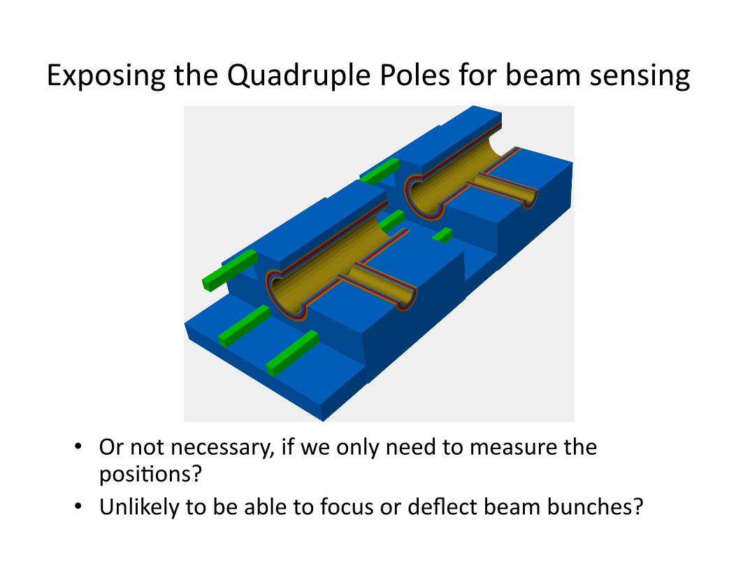
Exposing  the  Quadruple  Poles  for  beam  sensing    

•  Or  not  necessary,  if  we  only  need  to  measure  the  posi=ons?  

•  Unlikely  to  be  able  to  focus  or  deflect  beam  bunches?  

Page 16: SurveyonPhotonicsandNovel Op6cal’Materials’ · SurveyonPhotonicsandNovel Op6cal’Materials’ Minghao(Qi(Purdue(University(DLA2011 SLAC(Naonal(Accelerator(Laboratory(September15,2011

Fiber  Pigtailing  

•  The  hollow  coupler  could  be  short  and  tapered  •  Fiber  =ps  could  be  tapered  •  Add  heater  to  achieve  tunability  

TE mode

Short coupler

Page 17: SurveyonPhotonicsandNovel Op6cal’Materials’ · SurveyonPhotonicsandNovel Op6cal’Materials’ Minghao(Qi(Purdue(University(DLA2011 SLAC(Naonal(Accelerator(Laboratory(September15,2011

Fiber  to  Waveguide  Coupling  •  Fiber  splicing  <  0.1dB  (>  97.7%  power  coupling)  

•  Fiber  to  waveguides  on  chip  – Pigtailed  fiber  in  V-­‐grooves  –  Inverse  taper  

•  Gra=ng  couplers  – ~70%  coupling  in  a  CMOS  line  using  Si  based  structures  

– SiN  gra=ng  couplers  with  ~60%  efficiency  – 82%  in  theory  

Page 18: SurveyonPhotonicsandNovel Op6cal’Materials’ · SurveyonPhotonicsandNovel Op6cal’Materials’ Minghao(Qi(Purdue(University(DLA2011 SLAC(Naonal(Accelerator(Laboratory(September15,2011

Inverse  Taper  for  Fiber  to  Waveguide  Coupling  

•  ~  1dB  loss  per  facet  is  predicted  •  ~1.6dB  per  facet  loss  realized  

overcladding Silicon  or  SiN  core

Silicon  waveguides

Polymer  waveguides Doped  Silicon  dioxide  core  

Undercladding

Page 19: SurveyonPhotonicsandNovel Op6cal’Materials’ · SurveyonPhotonicsandNovel Op6cal’Materials’ Minghao(Qi(Purdue(University(DLA2011 SLAC(Naonal(Accelerator(Laboratory(September15,2011

Gra=ng  Coupler:  Ver=cal  to  Horizontal  coupling  

Page 20: SurveyonPhotonicsandNovel Op6cal’Materials’ · SurveyonPhotonicsandNovel Op6cal’Materials’ Minghao(Qi(Purdue(University(DLA2011 SLAC(Naonal(Accelerator(Laboratory(September15,2011

Gra=ng  coupler  achieving  -­‐1.6dB/coupler  

•  D.  Vermeulen,  et  al,  Op=cs  Express,  18,  18278,  2010  

Page 21: SurveyonPhotonicsandNovel Op6cal’Materials’ · SurveyonPhotonicsandNovel Op6cal’Materials’ Minghao(Qi(Purdue(University(DLA2011 SLAC(Naonal(Accelerator(Laboratory(September15,2011

220nm

150nm 220nm

370nm

240nm

Design  op=miza=on  

Ziran’s Design

Page 22: SurveyonPhotonicsandNovel Op6cal’Materials’ · SurveyonPhotonicsandNovel Op6cal’Materials’ Minghao(Qi(Purdue(University(DLA2011 SLAC(Naonal(Accelerator(Laboratory(September15,2011

Fabricated  Si  Gra=ng  Coupler  

Page 23: SurveyonPhotonicsandNovel Op6cal’Materials’ · SurveyonPhotonicsandNovel Op6cal’Materials’ Minghao(Qi(Purdue(University(DLA2011 SLAC(Naonal(Accelerator(Laboratory(September15,2011

Tes=ng  setup:  fiber  bundle  

Page 24: SurveyonPhotonicsandNovel Op6cal’Materials’ · SurveyonPhotonicsandNovel Op6cal’Materials’ Minghao(Qi(Purdue(University(DLA2011 SLAC(Naonal(Accelerator(Laboratory(September15,2011

Material  Guidelines  •  High  power  handling  capability  

– High-­‐damage  threshold  

– Low  nonlinearity  •  Conduc=vity:  avoid  electron  trapping  

– Dielectrics  – Semiconductor  

– Metal  – Graphene?  

•  CMOS  compa=bility  – SiO2,  SiN,  Si  

•  Other  semiconductors  or  exo=c  materials?  

Page 25: SurveyonPhotonicsandNovel Op6cal’Materials’ · SurveyonPhotonicsandNovel Op6cal’Materials’ Minghao(Qi(Purdue(University(DLA2011 SLAC(Naonal(Accelerator(Laboratory(September15,2011

Material  Damage  •  Con=nuous  wave  laser  characteriza=on  of  gra=ng  couplers  – Can  extract  power  enhancement  factor  from  resonant  structures.  

•  Si  has  high  two-­‐photon  absorp=on  probability  – Generates  free  carriers  – Absorbs  light  – Heat  up  structures  

•  Silicon  nitride  has  larger  band  gap  and  does  not  suffer  from  two-­‐photon  absorp=on  – Expected  to  have  much  higher  damage  threshold  

Page 26: SurveyonPhotonicsandNovel Op6cal’Materials’ · SurveyonPhotonicsandNovel Op6cal’Materials’ Minghao(Qi(Purdue(University(DLA2011 SLAC(Naonal(Accelerator(Laboratory(September15,2011

Silicon  Nitride  Waveguides  •  570nm Si3N4 by LPCVD •  3um buried silicon dioxide (BOX) •  4.5um Top Oxide Cladding by PECVD

SEM Picture is taken after Si3N4 etch. Sidewall has a slope of about 78°. HSQ is the etch mask

Oxide  Cladding  

BOX  

Si3N4  

Si  

Si3N4

HSQ

BOX

Etching Profile

Page 27: SurveyonPhotonicsandNovel Op6cal’Materials’ · SurveyonPhotonicsandNovel Op6cal’Materials’ Minghao(Qi(Purdue(University(DLA2011 SLAC(Naonal(Accelerator(Laboratory(September15,2011

Nitride  Ring  R=40um  with  Taper  

•  WG  width  =  1um  

•  Gap  =  700nm  

•  3dB bandwidth at 1558nm is about 7pm. •  Q ≈ 223K low propagation loss ~ 2dB/cm •  Grating couplers with SiN is being fabricated

Page 28: SurveyonPhotonicsandNovel Op6cal’Materials’ · SurveyonPhotonicsandNovel Op6cal’Materials’ Minghao(Qi(Purdue(University(DLA2011 SLAC(Naonal(Accelerator(Laboratory(September15,2011

On-­‐Chip  power  splipng:  SOI  Y-­‐junc=on  

•  Flat  power  splipng  across  a  large  bandwidth  

•  Arbitrary  splipng  ra=o?  

•  Post-­‐fabrica=on  trimming?  

Port#1

Port#2

Port#3

10dBm input power

Page 29: SurveyonPhotonicsandNovel Op6cal’Materials’ · SurveyonPhotonicsandNovel Op6cal’Materials’ Minghao(Qi(Purdue(University(DLA2011 SLAC(Naonal(Accelerator(Laboratory(September15,2011

Woodpile 3D Photonic Crystals •  Best flexibility in

designing hollow waveguides

•  17 layers are needed

Layer  7

300  nm Si  substrate

HSQ

6

1 2 3 4

5

100  nm

100  nm 300  nm

Page 30: SurveyonPhotonicsandNovel Op6cal’Materials’ · SurveyonPhotonicsandNovel Op6cal’Materials’ Minghao(Qi(Purdue(University(DLA2011 SLAC(Naonal(Accelerator(Laboratory(September15,2011

Membrane Transfer Technique 1. Fabricate all 17 layers in one step

+

+

+

2. Assemble layers to form 3D photonic crystal

waveguide

Page 31: SurveyonPhotonicsandNovel Op6cal’Materials’ · SurveyonPhotonicsandNovel Op6cal’Materials’ Minghao(Qi(Purdue(University(DLA2011 SLAC(Naonal(Accelerator(Laboratory(September15,2011

Woodpile structures before release

•  Grating lines may stick together due to capillary forces –  May need more spacers

Page 32: SurveyonPhotonicsandNovel Op6cal’Materials’ · SurveyonPhotonicsandNovel Op6cal’Materials’ Minghao(Qi(Purdue(University(DLA2011 SLAC(Naonal(Accelerator(Laboratory(September15,2011

Structures Released Successfully and Can be Stacked up

•  The residuals are water debris and can be eliminated. •  2nd layer does not have the same debris.

Page 33: SurveyonPhotonicsandNovel Op6cal’Materials’ · SurveyonPhotonicsandNovel Op6cal’Materials’ Minghao(Qi(Purdue(University(DLA2011 SLAC(Naonal(Accelerator(Laboratory(September15,2011

Two layer Woodpile Structures with Reasonable Alignment

•  Small particles within the membrane region. Can be avoided, we think.

Page 34: SurveyonPhotonicsandNovel Op6cal’Materials’ · SurveyonPhotonicsandNovel Op6cal’Materials’ Minghao(Qi(Purdue(University(DLA2011 SLAC(Naonal(Accelerator(Laboratory(September15,2011

Advantages •  Every layer has the exact thickness

–  They are from the same film

•  No patterning for each layers –  One can produce 100s or 1000s layers

in one wafer

•  No stress problem –  Assembly done in room temperature

•  For 9mm (CO2 laser) operating wavelength, can use optical lithography for patterning and alignment –  Period is 4.2 mm, rod width 1.2 mm,

and layer thickness 1.6 mm

500  nm  Silicon  

Layer  1  Layer  2  

Page 35: SurveyonPhotonicsandNovel Op6cal’Materials’ · SurveyonPhotonicsandNovel Op6cal’Materials’ Minghao(Qi(Purdue(University(DLA2011 SLAC(Naonal(Accelerator(Laboratory(September15,2011

3 Layer Membrane Bonding

•  High precision alignment is required

1  2  Layer  3  Layer  1  

Layer  2  Layer  3  

Page 36: SurveyonPhotonicsandNovel Op6cal’Materials’ · SurveyonPhotonicsandNovel Op6cal’Materials’ Minghao(Qi(Purdue(University(DLA2011 SLAC(Naonal(Accelerator(Laboratory(September15,2011

Questions?