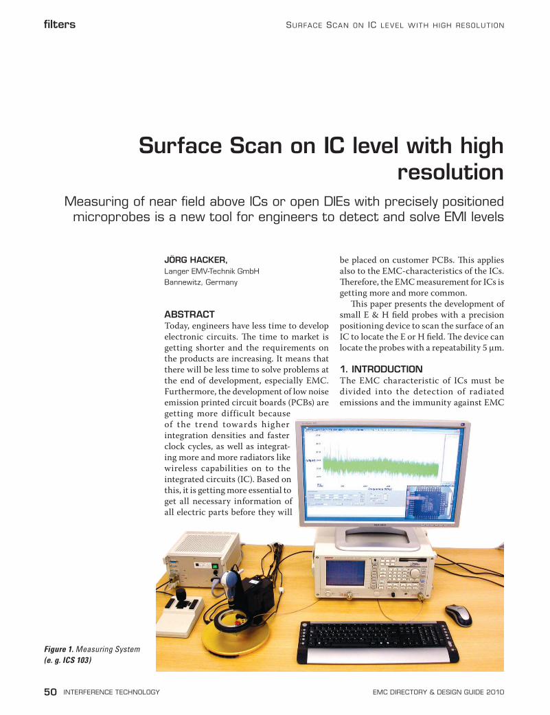
50 INTERFERENCE TECHNOLOGY EMC DIRECTORY & DESIGN GUIDE 2010 S URFACE S CAN ON IC LEVEL WITH HIGH RESOLUTION filters JÖRG HACKER, Langer EMV-Technik GmbH Bannewitz, Germany ABSTRACT Today, engineers have less time to develop electronic circuits. e time to market is getting shorter and the requirements on the products are increasing. It means that there will be less time to solve problems at the end of development, especially EMC. Furthermore, the development of low noise emission printed circuit boards (PCBs) are getting more difficult because of the trend towards higher integration densities and faster clock cycles, as well as integrat- ing more and more radiators like wireless capabilities on to the integrated circuits (IC). Based on this, it is getting more essential to get all necessary information of all electric parts before they will be placed on customer PCBs. is applies also to the EMC-characteristics of the ICs. erefore, the EMC measurement for ICs is getting more and more common. is paper presents the development of small E & H field probes with a precision positioning device to scan the surface of an IC to locate the E or H field. e device can locate the probes with a repeatability 5 µm. 1. INTRODUCTION The EMC characteristic of ICs must be divided into the detection of radiated emissions and the immunity against EMC Surface Scan on IC level with high resolution Measuring of near field above ICs or open DIEs with precisely positioned microprobes is a new tool for engineers to detect and solve EMI levels Figure 1. Measuring System (e. g. ICS 103)

Welcome message from author
This document is posted to help you gain knowledge. Please leave a comment to let me know what you think about it! Share it to your friends and learn new things together.
Transcript
50 INTERFERENCE TECHNOLOGY EMC DIRECTORY & DESIGN GUIDE 2010
Surface Scan on Ic level wIth hIgh reSolut Ionfilters
JÖRG HACKER, Langer EMV-Technik GmbH Bannewitz, Germany
ABSTRACT Today, engineers have less time to develop electronic circuits. The time to market is getting shorter and the requirements on the products are increasing. It means that there will be less time to solve problems at the end of development, especially EMC. Furthermore, the development of low noise emission printed circuit boards (PCBs) are getting more difficult because of the trend towards higher integration densities and faster clock cycles, as well as integrat-ing more and more radiators like wireless capabilities on to the integrated circuits (IC). Based on this, it is getting more essential to get all necessary information of all electric parts before they will
be placed on customer PCBs. This applies also to the EMC-characteristics of the ICs. Therefore, the EMC measurement for ICs is getting more and more common.
This paper presents the development of small E & H field probes with a precision positioning device to scan the surface of an IC to locate the E or H field. The device can locate the probes with a repeatability 5 µm.
1. INTRODUCTION The EMC characteristic of ICs must be divided into the detection of radiated emissions and the immunity against EMC
Surface Scan on IC level with high resolution
Measuring of near field above ICs or open DIEs with precisely positioned microprobes is a new tool for engineers to detect and solve EMI levels
Figure 1. Measuring System (e. g. ICS 103)

hacker
interferencetechnology.com INTERFERENCE TECHNOLOGY 51
filters
disturbance. This paper will discuss the detection of electromagnetic disturbance above ICs and open DIE with near-field microprobes. According to international EMC standards for ICs, near-field microprobes are used that clearly exceed IEC standard requirements (as defined in IEC 61697-3) in terms of their measurement parameters, such as resolution and frequency range. They allow the developers to measure electromagnetic disturbance emission on IC and open DIE and precisely localize the respective field sources in the IC or DIE. IC redesign could be planned on a better knowledge of the EMC issues in the IC and the final result could be verified with provable measurements. Therefore, it is possible to reduce the cost and the time for the devel-opment of new IC or redesign. Also for the developer of electrical circuits based on IC a precise detection of radiated emission above the IC is clearly with a benefit. With this information, it is possible to conclude for the PCB, e.g. which signal should be additionally shielded or which signal/pin is not critical for the radiation. For this purpose, Langer EMV developed near-field microprobes based on IEC 61697-3, to detect electromagnetic fields with a preci-sion in the µm-range of the IC's surface. Due to their high resolution and sensitivity, the near-field microprobes can no longer be guided by hand but must be precisely moved by a scanner system.
2. MEASURING SYSTEM Measuring spatial amplitude-frequency characteristics of electromagnetic emissions requires an IC test system architecture with the following components: 1. Near-field Microprobes 2. Scanner 3. Spectrum Analyzer
Figure 2. Test result of a Volume Scan, shown frequency: 200 MHz
The largest range of impulse test equipment up to 100kV and 100kA A Swiss Company [email protected] www.emc-partner.com
ESD
EFT / Burst
CWG / Surge
Magnetic Fields
Power Fail
Common Mode
Compact Transient Generator
PARTNEREMC -
TRA3000
A Swiss Company [email protected] www.emc-partner.com
NEWWebServerSave to USB Ethernet Atmospheric

52 INTERFERENCE TECHNOLOGY EMC DIRECTORY & DESIGN GUIDE 2010
Surface Scan on Ic level wIth hIgh reSolut Ionfilters
4. PC + Software (e. g. ChipScan) Figure 1 shows a schematic diagram of IC test system
setup for measurements based on the surface scan method in accordance with IEC 61967-3.
Three types of Microprobes are necessary to detect the entire electromagnetic field with a location accuracy in the µm range. To achieve this, Langer EMV developed several microprobes, each probe for a special case. The E-field probes are built to detect the electrical field. H-field probes are built to measure the magnetic field. Two mag-netic field probes are required; they differ in their plane of polarization: The „H„ type H-field probe has a horizontal polarization and the „V„ type H-field probe has a vertical polarization. The directional pattern of the vertically polar-
Figure 3. Types of probe tips, a - E-field, b - vertical H-field, c - horizontal H-field
Figure 4. General application layout
Figure 5. Set up for current measurement
ized H-field probe has two zero values for physical reasons. The field components located in the plane of the vertical probe can only be detected by rotating the HV-field probe.
The Scanner brings the microprobes in position with a high mechanical resolution and high repeatability. For measuring an electromagnetic field with high resolution the accuracy should be at least 20 µm and the repeatability less than 5 µm. At least four axes are necessary to com-pletely detect EMC emissions from the IC. Three axes are required for the movement in X-, Y- and Z-direction and the fourth is to rotate the microprobe, which is necessary for the vertical H-field probe.
The basic design of the microprobes is constructed to accomodate the Langer EMV Scanner. Furthermore, the mounting option of the microprobes was built to fit the common scanner systems.
The third part of the measuring system is a PC with a controlling and measuring software. Functions are: (1)de-tection of all connecting devices; (2) control of the scanner system; (3) initialization of the spectrum analyzer; (4) de-tection of the measuring results of the spectrum analyzer; and (5) visualization of the measuring results in a descrip-tive way. EMC emission measurements on ICs provide large quantities of data which are compiled in six dimensions in a database. Not all six dimensions can be represented graphically at the same time, so that the representation is therefore reduced to feasible five dimensions.
Figure 2 shows an example for a volume scan over an IC with a horizontal H-field probe.
The software allows executing automatic scans. Each scan volume could be easily defined via scripts and can be executed in ChipScan.
3. NEAR-FIELD MICROPROBES
3.1 Probe Design The IEC 61697-3 describes the parameters of microprobes, for example the mechanical construction, frequency range and resolution. According to the norm, the probe tip con-sists of a semi-rigid cable with a single coil for measuring the electromagnetic emissions. The disadvantage of this measuring setup is, it could not differentiate between the measured voltage at the probe tip and the magnetic or electrical field. Because of this Langer EMV designed two different types of microprobes, one type for measuring the electrical field and the second for measuring the magnetic field. The magnetic field probes are additionally shielded against coupling of the electric field. Therefore, the micro-probes allow the user to separately examine the electrical and the magnetic emissions on IC and DIE surfaces, e. g. bonding wires and pins. It is also possible to measure with a magnetic probe above a conductor or IC-Pin and to make a conclusion about the current, which flows through the conductor.
Currently the smallest position resolution that could be achieved with an E-field probe is 65 µm. Figure 3a shows the general construction of an E-field probe. The electri-

hacker
interferencetechnology.com INTERFERENCE TECHNOLOGY 53
filters
Figure 6. Measuring example - stripline
cal field strength is detected between the electrode on the probe tip and the shield-ing of the probe tip.
The resolution of the H-field probes is defined by their inside diameter. The magnetic probe tips consist of a coil with specified winding and inside diameter, refer to Figure 3b and 3c. Both these pa-rameters basically define the size of mag-netic field (resolution) and the strength which is detected. Today the smallest inside diameter is specified at 150 µm, for horizontal and vertical polarization. This results in a position resolution of the measured magnetic field of 80 µm. In the future there will be a smaller resolu-tion possible, approximately 60 µm or less with a probe diameter of 100 µm. All magnetic probes are shielded against coupling from the electrical field.
All microprobes are equipped with an internal 30 dB pre-amplifier. The amplifier allows to detect low signals clearly. The frequency range of the microprobes is calibrated from 1 MHz up to 3 GHz. This range will be extended to a higher frequency to accom-modate the IC development with higher clock frequencies.
Magnetic field strength and current determination The magnetic field strength HRF in the magnetic field probe coil can be calculated from the voltage output signal UProbe of the magnetic field probe by means of the calibration
54 INTERFERENCE TECHNOLOGY EMC DIRECTORY & DESIGN GUIDE 2010
Surface Scan on Ic level wIth hIgh reSolut Ionfilters
characteristic. The correction factor KH of the magnetic field probe is independent of the measurement geometry in each individual application,
i.e. the probe can be guided at an arbitrary distance and
angle relative to the electric conductor without any correc-tion error (Figure 4). The result is the average magnetic field that is coupling to the probe coil.
CURRENT CORRECTION: There is a consistent physical correlation between the magnetic field HRF and the current IRF which depends on the geometry of the current conductor layout. The given correction factor KI thus refers to a defined reference setup.
The determined current values ICorr are only correct if the geometric parameters coincide with the reference setup (Fig. 5) when the probes are used. If there are deviations from this setup, the current values ICorr will also deviate. The calculated current value ICorr can only be used as an orientation value.
Use of the correction factor KI in the adapted quantity equation:
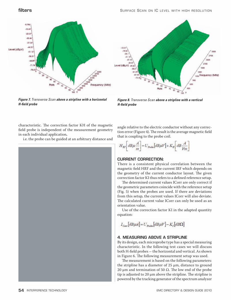
4. MEASURING ABOVE A STRIPLINE By its design, each microprobe type has a special measuring characteristic. In the following test cases we will discuss both H-field probes - the horizontal and vertical. As shown in Figure 6. The following measurement setup was used.
The measurement is based on the following parameters: the stripline has a diameter of 25 µm, distance to ground 20 µm and termination of 50 Ω. The low end of the probe tip is adjusted to 20 µm above the stripline. The stripline is powered by the tracking generator of the spectrum analyzer
Figure 7. Transverse Scan above a stripline with a horizontal H-field probe
Figure 8. Transverse Scan above a stripline with a vertical H-field probe
hacker
interferencetechnology.com INTERFERENCE TECHNOLOGY 55
filters
with a voltage level of 100 dBµV. The probe was moving above the stripline on a line with length 3 mm and the measuring steps were 30 µm. Figure 7 and Figure 8 show the measurement results for both H-field types. For each measurement point (plot) the amplitude with reference to the frequency is indicated.
It can be easily seen, both probe types are measuring in a different way. The horizontal probe measures a minimum at the center of the stripline. Intensive magnetic fields are
located at the edges of the stripline, which is also the site of the respective local maximum values of the scan volume. This behavior depends on the direction of the magnetic field lines and on the position of the measuring coil in relation to the field lines. At positions where the coil is parallel to the field lines, the probe could not detect a magnetic field. Only the electrical field is measured.
Unlike the horizontal polarized probe, the vertical probe measures a high magnetic field strength over the conduc-tor path. At the edges of the stripline, the vertical version measures a local minimum.
In each test case the amplitude and the width of a mea-sured minimum or maximum depend on the distance of the probe tip to the measuring object and the width of a measured stripline or any other electrical line. With the knowledge of the ratio of electrical field in comparison to magnetic field, each magnetic microprobe can be qualified.
5. IC-SCAN
5.1 IC-Volume Scan In the following test case two surface scans were per-formed on an IC. The DUT was a 8051-model from Maxim - DS89C430, system clock at 20 MHz.
The first Scan was done with a horizontal H-field probe and the second scan with a vertical one. The following set-
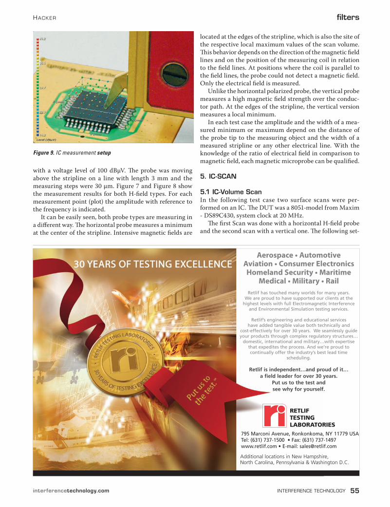
Figure 9. IC measurement setup
Additional locations in New Hampshire, North Carolina, Pennsylvania & Washington D.C.
795 Marconi Avenue, Ronkonkoma, NY 11779 USATel: (631) 737-1500 • Fax: (631) 737-1497www.retlif.com • E-mail: [email protected]
Aerospace • AutomotiveAviation • Consumer Electronics Homeland Security • Maritime
Medical • Military • RailRetlif has touched many worlds for many years.
We are proud to have supported our clients at thehighest levels with full Electromagnetic Interference
and Environmental Simulation testing services.
Retlif’s engineering and educational services have added tangible value both technically and
cost-effectively for over 30 years. We seamlessly guideyour products through complex regulatory structures…
domestic, international and military…with expertisethat expedites the process. And we’re proud tocontinually offer the industry’s best lead time
scheduling.
Retlif is independent…and proud of it…a field leader for over 30 years.
Put us to the test and see why for yourself.
7233 Retlif ITEM EMC Half_4c 4/30/09 11:28 AM Page 1

56 INTERFERENCE TECHNOLOGY EMC DIRECTORY & DESIGN GUIDE 2010
Surface Scan on Ic level wIth hIgh reSolut Ionfilters
tings were met: • Scan Volume: 11.0 x 11.0 mm • Step width: 200 µm • Measured spectra 10.000 • Points per spectrum 500
The driving of the scanner, the detection and the interpretation of the measuring results were done by ChipScan software.
Figure 9 shows the measurement setup. As it is shown, the IC was mounted on a ground plane. All other electrical parts were mounted on the back of the ground plane. This setup helps to minimize boundary effects from other electrical parts. Three pins were used for driving LEDs to monitor the program. All other pins were programmed as inputs.
The measurement results are illustrated in Figure 10 and Figure 11. The bar on the right side of both screen-
shots shows the relation between colour and strength of magnetic field. Red means a high signal strength of about 80 dBµV and blue stands for 20 dBµV (of the probe output).
Both measurements were done above the same DUT, but with different probes. As we discussed in chapter 4, the horizontal H-field probe measures directly above with the current runs a local minimum, and on the edges a local maximum. These can also be clearly seen in Fig. 11. From the VCC Pin the supply current flows via the bond conductor into the IC. At the chip the current takes different paths and is returned via the bond conductor and the VSS Pin to the board.
The vertical H-field Probe could only measure the magnetic field, where the current flows parallel to the probe measuring coil. There are some locations where the magnetic field is measured, especially in the power supply region of the IC. In other locations of the IC the microprobe is hardly detecting a magnetic field. Maybe
there is no magnetic field or the magnetic field is not in the sensitive probe direction. As a consequence of this, there should be done a second measurement, where the measuring coil (microprobe) is turned by an angle of 90°. This way the magnetic field could be detected, which is located 90° to the first measured one.
If such a surface scan is done with different dis-tances to the IC the magnetic field can be displayed in the entire volume above the IC. In Figure 12 all points with the same probe voltage output are displayed.
This diagram is very helpful for examining the coupling effects from the IC to other metallic parts which could be placed near to the IC in real applica-tions – e.g. heat sink, connectors, shielding parts.
5.2 IC-Pin Scan Using a vertical H-field probe offers the additional opportunity to measure the high frequency current flowing trough IC-pins. By using the basic measure-
ment setup shown in Figure 4, it is very simple to place the
Figure 10. Surface Scan over Test IC with vertical H-field probe, shown frequency 40MHz
Figure 11. Surface Scan over Test IC with horizontal H-field probe, shown frequency 40MHz
Figure 12. Surface Scan over Test IC with horizontal H-field probe, shown frequency is 40MHz

hacker
interferencetechnology.com INTERFERENCE TECHNOLOGY 57
filters
probe automatically close to every IC-pin and measure the current. One result is shown in Figure 13.
Typically each pin of an IC can be a source of high fre-quency current – power- and output-pins as well as input-pins. It depends on the IC itself and the impedance of the connected electronic circuit. Therefore, the knowledge of these currents enables the designer of the board the op-portunity to place series resistors or capacitors to GND in an optimal way.
6. CONCLUSION In this paper a measurement method to detect the probe output representing the magnetic and electric field in the location of the EUT in the µm-range is shown. It is shown that the measuring of near field above the ICs or open DIEs with precisely positioned microprobes is a new tool for engi-neers to detect EMI levels and to solve these in a reliable way. The measurement was done on reference PCB-assemblies or on the customer PCBs.
In the future there are a lot of opportunities to improve the measurement of electromagnetic fields in the µm range. With a smaller resolution, the detection over DIEs could be done more precisely; therefore smaller parts of integrated circuits could be scanned with a higher resolution. The frequency range must be increased. Because of higher clock cycles the product standards will be increased, so therefore there will be a requirement of EMI disturbance measure-ments to be performed in the higher frequency range above 3 GHz.
Today, a lot of simulation is performed on the EMC behavior of ICs. Right now it is not possible to compare simulation results with measuring results.
7 REFERENCES • [1] www.langer-emv.de • [2] product description MAXIM DS89C430: http://www.maxim-ic.
com/appnotes.cfm/an_pk/2
YOUR WEEKLY EMC UPDATE!
Interference Technology eNews provides news, standards updates, buyers guides,
product developments and more direct to your inbox once a week. Join the growing number
of subscribers to stay up to date – subscribe online today.
Sign up today at www.interferencetechnology.com
ITEM™
Figure 13. Result of a pin-scan
Related Documents