Surface plasmons in terahertz metamaterials G. Acuna 1 , S. F. Heucke 1 , F. Kuchler 1 , H.-T. Chen 2 , A. J. Taylor 2 , and R. Kersting 1 1 Photonics and Optoelectronics Group & Center for NanoScience, University of Munich, 80799 Munich, Germany 2 Los Alamos National Laboratory, MPA-CINT, MS K771, Los Alamos,New Mexico 87545, USA [email protected] http://www.thz.physik.uni-muenchen.de Abstract: We characterize terahertz metamaterials by applying aperture- less near-field microscopy with a bandwidth that covers the entire spectral response of the structures. The observations agree with the interpretation of the fundamental mode of the metamaterial. But the high frequency resonance shows properties that deviate from the common interpretation. We show that the high frequency response is governed by surface plasmon excitations, which have a comparable oscillator strength as the fundamental mode. © 2008 Optical Society of America OCIS codes: (180.4243) Near-field microscopy; (300.6495) Spectroscopy, terahertz; (160.3918) Metamaterials References and links 1. J. Pendry and D. R. Smith, “Reversing light with negative refraction,” Phys. Today 57, 37-43 (2004). 2. V. M. Shalaev, “Optical negative-index metamaterials,” Nat. Photonics 1, 41-48 (2007). 3. J. B. Pendry, A. J. Holden, D. J. Robbins, and W. Stewart, “Magnetism from conductors and enhanced nonlinear phenomena,” IEEE Trans. Microwave Theory Tech. 47, 2075-2084 (1999). 4. G. Mie, “Beitr¨ age zur Optik tr¨ uber Medien, speziell kolloidaler Metall¨ osungen,” Ann. Phys. 25, 377-445 (1908). 5. C. Enkrich, M. Wegener, S. Linden, S. Burger, L. Zschiedrich, F. Schmidt, J. F. Zhou, T. Koschny, and C. M. Soukoulis, “Magnetic metamaterials at telecommunication and visible frequencies,” Phys. Rev. Lett. 95, 203901 (2005). 6. H. Raether, Surface plasmons on smooth and rough surfaces and on gratings (Springer tracts in modern physics, 1998). 7. E. Shamonina and L. Solymar, “Magneto-inductive waves supported by metamaterial elements: components for a one-dimensional waveguide,” J. Phys. D 37, 362-367 (2004). 8. H. Liu, D. A. Genov, D. M. Wu, Y. M. Liu, J. M. Steele, C. Sun, S. N. Zhu, and X. Zhang, “Magnetic plasmon propagation along a chain of connected subwavelength resonators at infrared frequencies,” Phys. Rev. Lett. 97, 243902 (5 pages) (2006). 9. H.-T.Chen, W.J. Padilla, J. M. O. Zide, A. C. Gossard, A. J. Taylor, and R. D. Averitt, “Active terahertz meta- material devices,” Nature (London) 444, 597-600 (2006). 10. T. Zentgraf, J. Dorfm¨ uller, C. Rockstuhl, C. E.R. Vogelsang, K. Kern, T. Pertsch, F. Lederer, and H. Giessen, “Amplitude- and phase-resolved optical near fields of split-ring-resonator-based metamaterials,” Opt. Lett. 33, 848-850 (2008). 11. H.-T. Chen, R. Kersting, and G. C. Cho, “Terahertz imaging with nanometer resolution,” Appl. Phys. Lett 83, 3009-3012 (2003). 12. F. Buersgens, G. Acuna, C. H. Lang, S. I. Potrebic, S. Manus, and R. Kersting, “Shear force control for a THz near field microscope,” Rev. Sci. Instrum. 78, 113701 (2007). (C) 2008 OSA 10 November 2008 / Vol. 16, No. 23 / OPTICS EXPRESS 18745 #101635 - $15.00 USD Received 16 Sep 2008; revised 23 Oct 2008; accepted 23 Oct 2008; published 29 Oct 2008

Welcome message from author
This document is posted to help you gain knowledge. Please leave a comment to let me know what you think about it! Share it to your friends and learn new things together.
Transcript

Surface plasmons in terahertzmetamaterials
G. Acuna1, S. F. Heucke1, F. Kuchler1, H.-T. Chen2, A. J. Taylor2, andR. Kersting1
1Photonics and Optoelectronics Group & Center for NanoScience, University of Munich,80799 Munich, Germany
2Los Alamos National Laboratory, MPA-CINT, MS K771, Los Alamos, New Mexico 87545,USA
http://www.thz.physik.uni-muenchen.de
Abstract: We characterize terahertz metamaterials by applying aperture-less near-field microscopy with a bandwidth that covers the entire spectralresponse of the structures. The observations agree with the interpretationof the fundamental mode of the metamaterial. But the high frequencyresonance shows properties that deviate from the common interpretation.We show that the high frequency response is governed by surface plasmonexcitations, which have a comparable oscillator strength as the fundamentalmode.
© 2008 Optical Society of America
OCIS codes: (180.4243) Near-field microscopy; (300.6495) Spectroscopy, terahertz;(160.3918) Metamaterials
References and links1. J. Pendry and D. R. Smith, “Reversing light with negative refraction,” Phys. Today 57, 37-43 (2004).2. V. M. Shalaev, “Optical negative-index metamaterials,” Nat. Photonics 1, 41-48 (2007).3. J. B. Pendry, A. J. Holden, D. J. Robbins, and W. Stewart, “Magnetism from conductors and enhanced nonlinear
phenomena,” IEEE Trans. Microwave Theory Tech. 47, 2075-2084 (1999).4. G. Mie, “Beitrage zur Optik truber Medien, speziell kolloidaler Metallosungen,” Ann. Phys. 25, 377-445 (1908).5. C. Enkrich, M. Wegener, S. Linden, S. Burger, L. Zschiedrich, F. Schmidt, J. F. Zhou, T. Koschny, and C. M.
Soukoulis, “Magnetic metamaterials at telecommunication and visible frequencies,” Phys. Rev. Lett. 95, 203901(2005).
6. H. Raether, Surface plasmons on smooth and rough surfaces and on gratings (Springer tracts in modern physics,1998).
7. E. Shamonina and L. Solymar, “Magneto-inductive waves supported by metamaterial elements: components fora one-dimensional waveguide,” J. Phys. D 37, 362-367 (2004).
8. H. Liu, D. A. Genov, D. M. Wu, Y. M. Liu, J. M. Steele, C. Sun, S. N. Zhu, and X. Zhang, “Magnetic plasmonpropagation along a chain of connected subwavelength resonators at infrared frequencies,” Phys. Rev. Lett. 97,243902 (5 pages) (2006).
9. H.-T. Chen, W. J. Padilla, J. M. O. Zide, A. C. Gossard, A. J. Taylor, and R. D. Averitt, “Active terahertz meta-material devices,” Nature (London) 444, 597-600 (2006).
10. T. Zentgraf, J. Dorfmuller, C. Rockstuhl, C. E. R. Vogelsang, K. Kern, T. Pertsch, F. Lederer, and H. Giessen,“Amplitude- and phase-resolved optical near fields of split-ring-resonator-based metamaterials,” Opt. Lett. 33,848-850 (2008).
11. H.-T. Chen, R. Kersting, and G. C. Cho, “Terahertz imaging with nanometer resolution,” Appl. Phys. Lett 83,3009-3012 (2003).
12. F. Buersgens, G. Acuna, C. H. Lang, S. I. Potrebic, S. Manus, and R. Kersting, “Shear force control for a THznear field microscope,” Rev. Sci. Instrum. 78, 113701 (2007).
(C) 2008 OSA 10 November 2008 / Vol. 16, No. 23 / OPTICS EXPRESS 18745#101635 - $15.00 USD Received 16 Sep 2008; revised 23 Oct 2008; accepted 23 Oct 2008; published 29 Oct 2008

13. H.-T. Chen, S. Kraatz, G. C. Cho, and R. Kersting, “Identification of a resonant imaging process in aperturelessnear-field microscopy,” Phys. Rev. Lett. 93, 267401 (2004).
14. M. Abashin, U. Levy, K. Ikeda, and Y. Fainman, “Effects produced by metal-coated near-field probes on theperformance of silicon waveguides and resonators,” Opt. Lett. 32, 2602-2604 (2007).
15. G. Acuna, F. Buersgens, C. H. Lang, M. Handloser, A. Guggenmos and R. Kersting, “Interdigitated terahertzemitters,” Elec. Lett. 44, 229-231 (2008).
16. W. J. Padilla, A. J. Taylor, C. Highstrete, M. Lee, and R. D. Averitt, “Dynamical electric and magnetic metama-terial response at terahertz frequencies,” Phys. Rev. Lett. 96, 107401 (2006).
17. R. Singh, E. Smirnova, A. J. Taylor, J. F. O’Hara, and W. Zhang, “Optically thin terahertz metamaterials,” Opt.Express 16, 6537-6543 (2008).
18. A. K. Azad, A. J. Taylor, E. Smirnova, and J. F. O’Hara, “Characterization and analysis of terahertz metamaterialsbased on rectangular split-ring resonators,” Appl. Phys. Lett. 92, 011119 (2008).
1. Introduction
Metamaterials offer outstanding opportunities for designing the electromagnetic properties ofmatter [1, 2]. Their response to light is determined by the structure embossed into the ma-terial rather than by its composition. The most common approach for tailoring electrical andmagnetic properties of the metamaterials is to design metallic resonators and arrange them inperiodic patterns [3]. Obviously, the unit cells of such patterns have to be smaller than thelight’s wavelength if a spatially homogeneous response in the far-field is desired. The primaryresonances of both, the dielectric permittivity and the magnetic susceptibility are determinedby the geometric properties of the elements within the unit cells. Examples are LC-resonancesof circuits comprising inductances and capacitances or Mie resonances within the individualmicroscopic elements [4, 5]. Besides these modes the periodicity of the structures itself maylead to further excitations with distinct resonances. Periodic patterns are known to support col-lective excitations such as dielectric plasmon polaritons [6] and magneto plasmon polaritons[7, 8]. These collective excitations can reach oscillator strengths, which are comparable to thatof the elements within the unit cell. In this work we identify the modes of metamaterials usingTHz microscopy with extreme subwavelength resolution. Our experimental data show, that onemode, which is commonly attributed to a Mie resonance, in fact results from surface plasmonexcitations. It is assumed that surface plasmon resonances are a generic property of virtuallyall metamaterials, because the only requirement for the excitation of these surface waves is theperiodicity of the metal structure.
2. Method
The experiments were performed on metamaterials that allow for switching the dielectric reso-nances by electronic means [9]. The schematic in Fig. 1(a) shows a typical structure and sum-marizes the most important dimensions. The array of electric split-ring resonators is fabricatedon a GaAs substrate with a 1 μm thick n-doped epitaxial layer. Further details of the structurecan be found in Ref. [9]. Electronic control over the optical properties is achieved by switchingthe width of the depletion zone underneath the surface of the structure. The metallic structureforms a Schottky contact to the electron gas in the GaAs as shown in Fig. 1(b). Without ap-plied bias, mobile electrons are close to the metallic structure, and short-circuit the element’scentral capacitor. When a positive bias is applied, the increased depletion width prevents short-circuiting and the structure reveals a resonance given by the capacitances and inductances of theloops. Far-field transmission data show two resonances when the polarization of the excitingfield is oriented as illustrated in Fig. 1(c). The resonance f A = 0.7 THz is due to the funda-mental mode, which oscillates between the terminals of the capacitor (mode α in the inset ofFig 1(c)). The resonance fB = 1.6 THz agrees with numerical calculations of a Mie-type modeat the side of the element (mode β in Fig. 1(c)). In the following, we show that the resonance
(C) 2008 OSA 10 November 2008 / Vol. 16, No. 23 / OPTICS EXPRESS 18746#101635 - $15.00 USD Received 16 Sep 2008; revised 23 Oct 2008; accepted 23 Oct 2008; published 29 Oct 2008

at this frequency in fact results from the collective excitation of the elements. The oscillatorstrength of this collective mode exceeds that of the Mie resonance and dominates the spectralresponse in this frequency range.
The advance of near-field microscopy makes it possible to resolve the modes along the el-ements of a metamaterial [10]. In this study, we apply apertureless terahertz near-field mi-croscopy with a spatial resolution of about 1 μm [11]. Further details of our technique and theelectro-optic detection can be found in [12]. Figure 2(a) illustrates the microscope head. Theincident THz pulses are concentrated by the tungsten probe to a spot size of about 1 μm under-neath the tip. This spot size is comparable to the lateral resolution of the microscope. It shouldbe emphasized that the image contrast in apertureless THz microscopy is proportional to thecapacitive coupling of the near-field into the structure underneath [13]. Thus, the spot size alsodefines the area where the metamaterial is locally excited by the near-field. This differs fromapertureless techniques operated in the near infrared and visible, where non-metallic probespick up field energy and emit it into the far-field [10, 14]. One outstanding strength of aperture-less THz microscopy is its band width. With our recently developed THz emitter [15], it extendsover more than 2 octaves from 0.5 THz to about 2.5 THz and covers the entire response spec-trum of the metamaterials investigated. This property allows for the spectral characterization ofthe local response, which is the main merit of this work.
Ohmic Schottky
E
H
a
b
c
0.5 1.0 1.5 2.0 2.50.0
0.2
0.4
0.6
0.8
1.0
Tra
nsm
issi
on
Frequency (THz)
a)
Mobile Carriers
Mobile Carriers
�U > 0 V
b)
c)
�U = 0 V
fA
fB
�U = 0 V
�U = 15 V
� �
Fig. 1. (a) Top view onto the metamaterial, which consists of a metallic structure fabricatedon n-doped GaAs, with a = 50 μm and b = c = 36 μm. (b) Cross section through the device.Application of a bias between ohmic contact and Schottky contact enlarges the depletionzone, which prevents short-circuiting of the capacitor. (c) Far-field transmission spectrafor two different biases. The inset illustrates the polarization of the incident light and twopossible modes within one element.
(C) 2008 OSA 10 November 2008 / Vol. 16, No. 23 / OPTICS EXPRESS 18747#101635 - $15.00 USD Received 16 Sep 2008; revised 23 Oct 2008; accepted 23 Oct 2008; published 29 Oct 2008

3. Results
Figure 2(b) shows the THz image of one element. All details of the metallic structure are re-solved with an image contrast of about 3%. Further insight into the spatial distribution of modesis obtained by differential THz imaging. The differential signal is recorded while the metama-terial is electronically switched between the on- and off-state. This image shows an enhancedcontrast close to the central capacitor, while other regions of the device show no measurablesignal. We interpret the data in terms of the capacitive coupling between scanning probe andstructure. The capacitive coupling is most efficient at the anti-nodes of the resonator, which arelocated at the capacitor. Here, the fundamental mode α is excited. Following this interpretation,the excitation of mode β should be visible at the edges of the structure. In contrast, no signifi-cant signal is recorded here, as Fig. 2(c) shows. From this unexpected fact we conclude that theMie-type mode β has an oscillator strength, which is much smaller than that of the fundamentalmode α . Apparently, the strong resonance at f B (see Fig. 1(c)) results from another mechanism,which couples much more efficiently to radiation.
Contrast [%]
0
0.5
1.0
1.5
2.0
Contrast [%]
0
0.5
1.0
1.5
2.0
2.5
3.0
3.5
TungstenProbe
ReflectedTHz Pulse
IncidentTHz Pulse
b)
c)
a)
10 µm
10 µm
Fig. 2. (a) Schematic of the apertureless THz microscope. The tungsten probe concentratesthe incident radiation to the area underneath the tip. (b) Terahertz near-field image of oneunit cell. The lateral resolution is about 1 μm. (c) Differential image obtained by switchingthe structure on and off. The dotted lines illustrate the position of the element.
(C) 2008 OSA 10 November 2008 / Vol. 16, No. 23 / OPTICS EXPRESS 18748#101635 - $15.00 USD Received 16 Sep 2008; revised 23 Oct 2008; accepted 23 Oct 2008; published 29 Oct 2008

In the following, we will show that the resonance at f B = 1.6 THz results from the collectiveresponse of the entire metamaterial. The extreme bandwidth of apertureless THz microscopyallows for recording the entire spectral response at distinct positions of the structure, as shownin Fig. 3. At position 1 the response of the fundamental mode at 0.7 THz should be strongestwhile the response of the Mie mode at 1.6 THz is expected to appear at position 2. However,this is not observed. No measurable response is observed at position 2, which confirms thatthe Mie-mode β has a smaller oscillator strength than the fundamental mode α . In fact, bothresonances are found at position 1, which makes a reinterpretation of the resonance at 1.6 THznecessary.
0.5 1.0 1.5 2.0 2.50.8
0.9
1.0
1.1
1.2D
iffere
ntia
lCouplin
g(n
orm
.)
Frequency (THz)
1
2
Fig. 3. Spectrally resolved coupling of the near-field to the metamaterial. The spectra wereobtained at two different positions of the metamaterial.
Fig. 4. Dispersion relation for surface plasmon excitations propagating on a metal/air in-terface and on a metal/GaAs interface. Coupling between light and surface plasmons ispossible at 1.6 THz, when an inverse lattice vector G = 2π
a is gained from the grating.
(C) 2008 OSA 10 November 2008 / Vol. 16, No. 23 / OPTICS EXPRESS 18749#101635 - $15.00 USD Received 16 Sep 2008; revised 23 Oct 2008; accepted 23 Oct 2008; published 29 Oct 2008
4. Discussion
The resonance at 1.6 THz results from the excitation of surface plasmons along the surface ofthe structure. Figure 4 illustrates the surface plasmon dispersion, which can be approximatedfor the THz range by ω = kc/
√ε , where c is the speed of light. At perpendicular incidence,
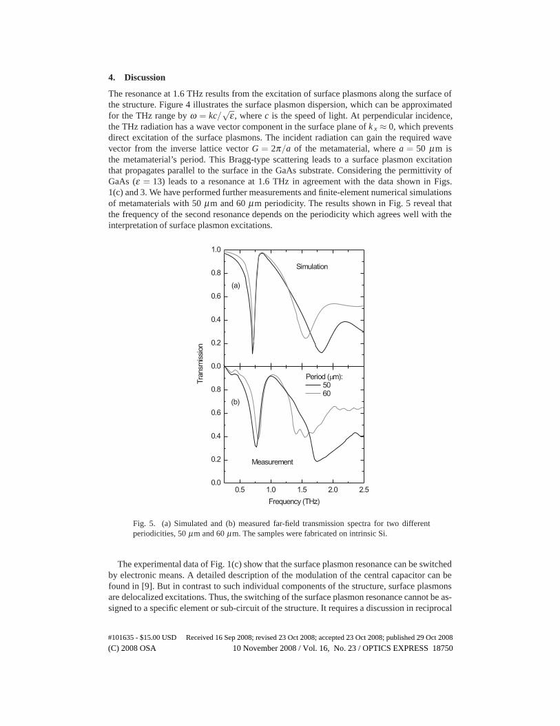
the THz radiation has a wave vector component in the surface plane of k x ≈ 0, which preventsdirect excitation of the surface plasmons. The incident radiation can gain the required wavevector from the inverse lattice vector G = 2π/a of the metamaterial, where a = 50 μm isthe metamaterial’s period. This Bragg-type scattering leads to a surface plasmon excitationthat propagates parallel to the surface in the GaAs substrate. Considering the permittivity ofGaAs (ε = 13) leads to a resonance at 1.6 THz in agreement with the data shown in Figs.1(c) and 3. We have performed further measurements and finite-element numerical simulationsof metamaterials with 50 μm and 60 μm periodicity. The results shown in Fig. 5 reveal thatthe frequency of the second resonance depends on the periodicity which agrees well with theinterpretation of surface plasmon excitations.
0.0
0.2
0.4
0.6
0.8
1.0
(b)
Measurement
Tra
nsm
issi
on
Period (�m):5060
Simulation
(a)
0.5 1.0 1.5 2.0 2.50.0
0.2
0.4
0.6
0.8
Frequency (THz)
Fig. 5. (a) Simulated and (b) measured far-field transmission spectra for two differentperiodicities, 50 μm and 60 μm. The samples were fabricated on intrinsic Si.
The experimental data of Fig. 1(c) show that the surface plasmon resonance can be switchedby electronic means. A detailed description of the modulation of the central capacitor can befound in [9]. But in contrast to such individual components of the structure, surface plasmonsare delocalized excitations. Thus, the switching of the surface plasmon resonance cannot be as-signed to a specific element or sub-circuit of the structure. It requires a discussion in reciprocal
(C) 2008 OSA 10 November 2008 / Vol. 16, No. 23 / OPTICS EXPRESS 18750#101635 - $15.00 USD Received 16 Sep 2008; revised 23 Oct 2008; accepted 23 Oct 2008; published 29 Oct 2008

space rather than in the original lattice. The electro-modulation of any periodic lattice propertyleads to a modulation at wave vector G = 2π/a in reciprocal space. At this inverse lattice vec-tor the surface plasmon couples to light. This modulation of Fourier components in reciprocalspace suffices for electromodulating the surface plasmon. In the micrographs (Fig. 2) and inthe spectral measurements in Fig. 3 the surface plasmon resonance has an enhanced visibilityin the region of the capacitor because here the electrical field energy is stored every half cycle.
Finally, it should be mentioned that the framework of surface plasmons in metamaterialsagrees with resonances reported in other works [16, 17, 18]. The fact that these works covera variety of metamaterial structures emphasizes the generic role of surface plasmons in THzmetamaterials.
5. Conclusions
In summary, we have shown that plasmonic resonances significantly affect the optical propertiesof metamaterials. The strength of plasmonic resonances can exceed that of Mie resonanceswithin the unit cell. The finding suggests that future design and interpretation of metamaterialsshould consider collective excitations.
Acknowledgments
This work is partially supported by the Nanosystems Initiative Munich (NIM), the InternationalDoctorate Program Nano-Bio-Technology (IDK-NBT) of the Elite Network of Bavaria, and bythe Deutsche Forschungsgemeinschaft (DFG), contract KE516/1-1. H.T.C and A.J.T acknowl-edge support from the Los Alamos National Laboratory LDRD Program and the Center forIntegrated Nanotechnologies, a U.S. Department of Energy, Office of Basic Energy SciencesNanoscale Science Research Center operated jointly by Los Alamos and Sandia National Lab-oratories. The authors acknowledge technical support by F. Buersgens, W. H. Nitsche, and S.Schloegl, and material growth by J. M. O. Zide and A. C. Gossard at UCSB.
(C) 2008 OSA 10 November 2008 / Vol. 16, No. 23 / OPTICS EXPRESS 18751#101635 - $15.00 USD Received 16 Sep 2008; revised 23 Oct 2008; accepted 23 Oct 2008; published 29 Oct 2008
Related Documents