SURFACE PLASMONIC CORE-SHELL PARTICLES FOR SOLAR ENERGY HARVESTING by Bo Ding ME, Zhejiang University, China, 2008 BE, Tianjin University, China, 2006 Submitted to the Graduate Faculty of the Swanson School of Engineering in partial fulfillment of the requirements for the degree of Doctor of Philosophy University of Pittsburgh 2014

Welcome message from author
This document is posted to help you gain knowledge. Please leave a comment to let me know what you think about it! Share it to your friends and learn new things together.
Transcript

SURFACE PLASMONIC CORE-SHELL PARTICLES FOR
SOLAR ENERGY HARVESTING
by
Bo Ding
ME, Zhejiang University, China, 2008
BE, Tianjin University, China, 2006
Submitted to the Graduate Faculty of
the Swanson School of Engineering in partial fulfillment
of the requirements for the degree of
Doctor of Philosophy
University of Pittsburgh
2014
ii
UNIVERSITY OF PITTSBURGH
SWANSON SCHOOL OF ENGINEERING
This dissertation was presented
by
Bo Ding
It was defended on
July 10th, 2013
and approved by
Jung-Kun Lee, PhD, Associate Professor, Department of Mechanical Engineering and
Materials Science
Paul W. Leu, PhD, Assistant Professor, Department of Industry Engineering
John A. Barnard, PhD, Professor, Department of Mechanical Engineering and Materials
Science
Ian Nettleship, PhD, Associate Professor, Department of Mechanical Engineering and
Materials Science
Guofeng Wang, PhD, Assistant Professor, Department of Mechanical Engineering and
Materials Science
Dissertation Director: Jung-Kun Lee, PhD, Associate Professor,
Department of Mechanical Engineering and Materials Science

iii
Copyright © by Bo Ding
2014

iv
Plasmonic core-shell particles, consisting of a spherical dielectric core coated with a concentric
layer of metallic nanoshell, are versatile subwavelength optical components. Their surface
plasmon resonance can be tuned by simply varying the thickness of the metallic nanoshell and
the diameter of the inner core. A facile two step method has been developed to synthesize core-
shell particles with well coated Ag nanoshell. Embedding these plasmonic core-shell particles
into TiO2 mesoporous photoelectrode enlarges the optical cross-section of dye sensitizers coated
onto the photoelectrode and increases the energy conversion efficiency of dye sensitized solar
cells (DSSCs). The enhanced photon-electron conversion is attributed to localized surface
plasmons of the core-shell particles, which increase the absorption and scattering of the incoming
light in the photoelectrode. We also show that the extinction spectra of the photoelectrode can be
effectively controlled by changing the geometric factor of the plasmonic particles. This tuning
capability allows us to design the surface plasmons of the core-shell particles to maximize the
absorption of the dye molecules with different optical absorption spectrum for dye sensitized
solar cells. In addition, simulation has been applied based on Mie scattering theory to
demonstrate the plasmon absorption and scattering effect of the core-shell particles. Furthermore,
we report that the light harvesting efficiency of PbS nanoparticle solar cells is significantly
increased by SiO2@Au@SiO2 plasmonic particles (SGSs). A mechanism underlying enhanced
light harvesting of F-doped SnO2 (FTO)/TiO2/PbS/Au heterojunction solar cells is investigated
SURFACE PLASMONIC CORE-SHELL PARTICLES FOR SOLAR ENERGY
HARVESTING
Bo Ding, PhD
University of Pittsburgh, 2014
v
using both experimental and theoretical methods. Finite-difference time-domain (FDTD)
simulation demonstrates that the effect of the plasmonic particles on the light absorption by PbS
nanoparticles depends on the location of the plasmonic particles. When SGSs are placed between
PbS and TiO2, nanodomes are formed on a top Au layer and additional light scattering at the
nanodomes is found. Our results demonstrate that SGSs can promote the light harvesting of the
thin film solar cells in two ways. The first enhancement effect is due to the localized surface
plasmon resonance of SGSs themselves and the second one is attributed to the increased
roughness of the top Au electrode with the nandomes.

vi
TABLE OF CONTENTS
LIST OF TABLES ...................................................................................................................... IX
LIST OF FIGURES……………………………………………………………........…………..X
PREFACE……………………………………………………………………………………...XX
1.0 INTRODUCTION ........................................................................................................ 1
1.0.1 Plasmonic Metal Nanoparticles ................................................................... 2
1.0.2 Plasmonic Dielectric Core-Metal Shell Nanostructures ............................ 3
1.1 DYE SENSITIZED SOLAR CELLS ................................................................. 5
1.2 APPLICATION OF THE PLASMONIC STRUCTURES .............................. 8
1.2.1 Photovoltaic ................................................................................................... 8
1.2.2 Other Applications. ..................................................................................... 10
1.2.2 .1 Surface-Enhanced Raman Spectroscopy .............................................. 10
1.2.2 .2 Photoacoustic Signal Nanoamplifiers .................................................... 11
1.3 CHALLENGES OF METALLIC CORE-SHELL PARTICLES ................. 13
2.0 OPTICAL SIMULATION OF PLASMONIC STRUCTURES .............................. 1
2.1 MOTIVATION .................................................................................................... 1
2.2 SIMULATION OF PLASMONIC CORE-SHELL PARTICLES ................ 18
2.2.1 Formulas for Optical Simulation of Silver Nanoparticles ...................... 18
2.2.2 Formulas for Optical Simulation of Ag@SiO2 Nanostructures ............. 21
vii
2.2.3 Results and Discussions .............................................................................. 22
3.0 SURFACE-PLASMON ASSISTED ENERGY CONVERSION IN DSSC .......... 27
3.1 BACKGROUND ................................................................................................ 27
3.1.1 Motivation .................................................................................................... 27
3.1.2 Electron Lifetime Measurement ................................................................ 29
3.1.3 Electrochemcial Impedance Spectroscopy ............................................... 33
3.2 PERFORMANCE ENHANCEMENT BY CORE-SHELL PARTICLES ... 36
3.2.1 Sample Preparation and Characterization ............................................... 36
3.2.2 Results and Discussions .............................................................................. 40
4.0 PLASMONIC TUNING EFFECT IN DSSC ........................................................... 57
4.1 BACKGROUND ................................................................................................ 57
4.2 TUNING EFFECT OF CORE-SEHLL PARTICLES IN DSSC .................. 60
4.2.1 Sample Preparation and Characterization ............................................... 60
4.2.2 Results and Discussions .............................................................................. 61
5.0 DUAL PLASMON ASSISTED LEAD SULFIDE SOALR CELLS ...................... 75
5.1 BACKGROUND ................................................................................................ 75
5.1.1 PbS QDs and Surface Ligands ................................................................... 78
5.1.2 Schottky Solar Cells Based on Lead Chalcogenide Film ......................... 81
5.1.3 PbS QDs Based Heterojunction Solar Cells ............................................. 85
5.1.4 X-ray Photoelectron Spectroscopy ............................................................ 89
5.2 DUAL PLASMON EFFECT IN HETEROJUNCTION SOLAR CELLS ... 90
5.2.1 Sample Preparation and Characterization ............................................... 90
5.2.2 Results and Discussions .............................................................................. 95
viii
6.0 CONCLUSIONS AND FUTURE WORK ............................................................. 115
6.1 CONCLUSIONS .............................................................................................. 115
6.2 FUTURE WORK ............................................................................................. 116
6.2.1 SGS Application in DSSCs with Low Temperature UV Annealing ..... 116
6.2.2 Applying MoOx Layer in Plasmon Assisted PbS QDs Solar Cells ....... 118
BIBLIOGRAPHY ..................................................................................................................... 120
ix
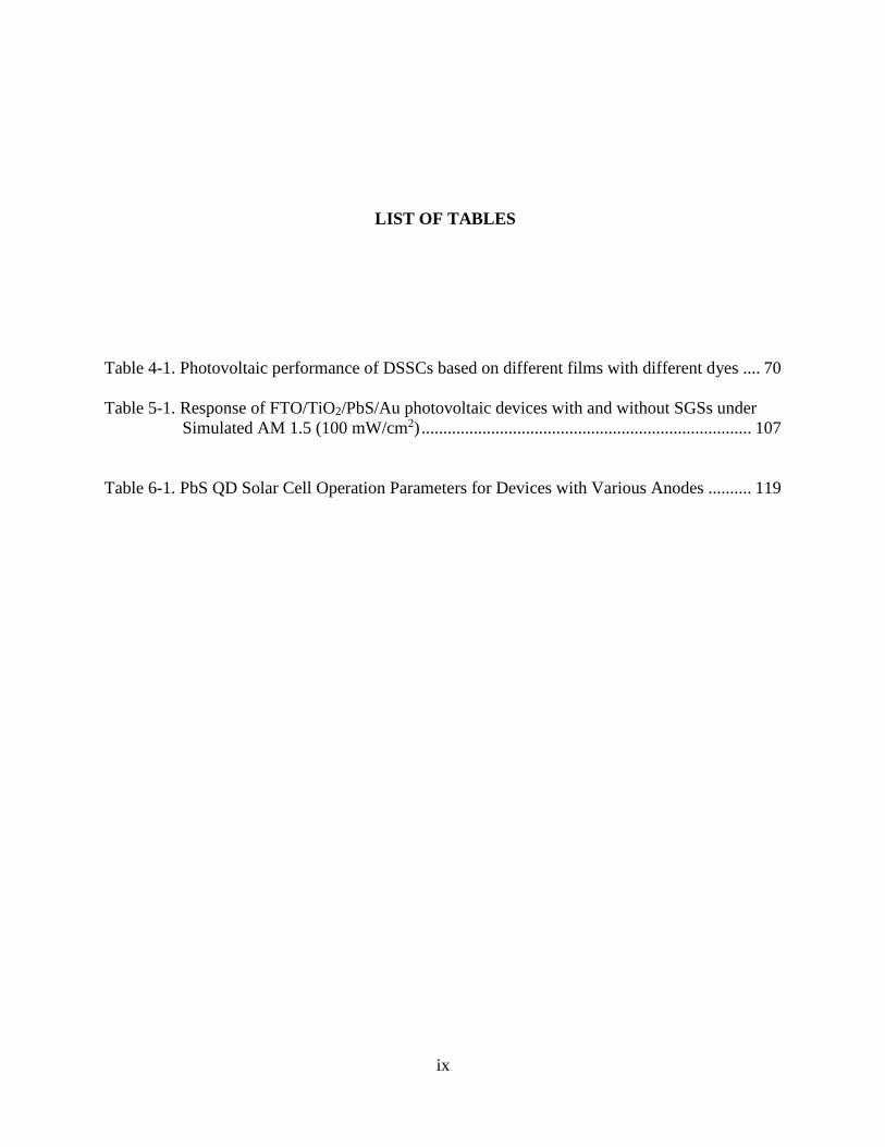
LIST OF TABLES
Table 4-1. Photovoltaic performance of DSSCs based on different films with different dyes .... 70
Table 5-1. Response of FTO/TiO2/PbS/Au photovoltaic devices with and without SGSs under
Simulated AM 1.5 (100 mW/cm2) ............................................................................ 107
Table 6-1. PbS QD Solar Cell Operation Parameters for Devices with Various Anodes .......... 119

x
LIST OF FIGURES
Figure 1-1. Schematic diagrams illustrating (a) a surface plasmon polariton and (b) a localized
surface plasmon .......................................................................................................... 3
Figure 1-2. Visual demonstration of the tunability of metal nanoshells (top), and optical spectra
of Au shell – silica core nanostructures as a function of their core/shell ratio .......... 4
Figure 1-3. Energy level diagrams (A) depicting plasmon hybridization in metal nanoshells
resulting from interacting sphere and cavity plasmons with two hybridized plasmon
modes and (B) illustrating the dependence of nanoshell plasmon energies ............... 5
Figure 1-4. DSSC structure and energy band alignment superposition diagram ........................... 7
Figure 1-5. Plasmonic light-trapping geometries for thin-film solar cells. .................................... 9
Figure 1-6. Left: microscope images of (a) stimulated and (b) unstimulated cells. Fluorescence
images of (c) stimulated and (d) unstimulated cells. Right: Photoacoustic imaging
system ....................................................................................................................... 12
Figure 1-7. TEM images of incomplete Ag nanoshells with silica cores .................................... 14
Figure 1-8. (Top) Molecule structures of N719 and black dyes. (Bottom left) Absorption spectra
of N719 and black dyes. (Bottom right) Prototype DSSCs employing N719 and
black dyes.................................................................................................................. 15
Figure 2-1. Calculated absorption efficiency (a) and scattering efficiency (b) of core-shell
particles using two different models ......................................................................... 24
Figure 2-2. UV-vis extinction spectra of theoretical data calculated by Mie scattering approach.
(A) 110 nm Ag@SiO2 core-shell particles in aqueous solution. (B) 470 nm
Ag@SiO2 core-shell particles in aqueous solution ................................................... 25
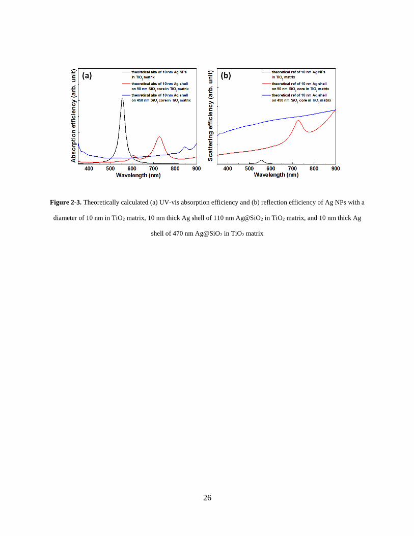
Figure 2-3. Theoretically calculated (A) UV-vis absorption efficiency and (B) reflection
efficiency of Ag NPs with a diameter of 10 nm in TiO2 matrix, 10 nm thick Ag shell

xi
of 110 nm Ag@SiO2 in TiO2 matrix, and 10 nm thick Ag shell of 470 nm Ag@SiO2
in TiO2 matrix ........................................................................................................... 26
Figure 3-1. Setup of OCVD measurement ................................................................................... 30
Figure 3-2 (a) Experimental Voc decay at different light intensities. (b) The electron lifetime
derived from eq. 3-1 as a function of Voc ................................................................... 31
Figure 3-3. Configuration of SLIM-PCV measurement .............................................................. 32
Figure 3-4. (left) Current responses and (right) voltage transients induced by different stepped
laser intensities .......................................................................................................... 33
Figure 3-5. Representations of the impedance of an equivalent circuit. R1 takes on values 5, 4, 2
kΩ, C1 = 10mF, τ1 = 50, 40, 20 s, R2 = 1 kΩ. (a) The equivalent circuit, (b) Nyquist
plot and (c) Bode plot ............................................................................................... 34
Figure 3-6. Equivalent circuits of DSSC, including (a) quantitative collection of photoinjected
electron and (b) incomplete electron collection. (c) Bode plot and (d) Nyquist plot of
DSSC using N719 dye .............................................................................................. 35
Figure 3-7. Schematic procedure of preparation Ag@SiO2 core-shell particles by a seed
mediated two-step method ........................................................................................ 37
Figure 3-8. TEM image of TiO2 nanoparticles that are prepared by a hydrothermal route ......... 38
Figure 3-9. Schematic structure of the device which contains the core-shell particles embedded
composite film .......................................................................................................... 39
Figure 3-10. TEM micrographs of (a) bare silica spheres, (b) silica particles coated with Ag
seeds, (c) two-step grown silica@Ag core-shell particles with the Ag layer being
deposited for 1 hr, and (d) two-step grown silica@Ag core-shell particles with the
Ag layer being deposited for 3 hrs (black scale bar in insets = 200 nm) ................ 41
Figure 3-11. SEM micrographs of (a) bare silica spheres, (b) silica particles coated with Ag
seeds, (c) two-step grown silica@Ag core-shell particles with the Ag layer being
deposited for 1 hr, and (d) two-step grown silica@Ag core-shell particles with the
Ag layer being deposited for 3 hrs .......................................................................... 42
Figure 3-12. XRD patterns of (a) bare silica, silica particles coated with Ag seeds, and silica
particles deposited with Ag layer for 1 hr, and (b) TiO2 nanoparticle and silica@Ag
core-shell particle mixture films that are annealed in N2 atmosphere at 400 oC for 1
hr ............................................................................................................................. 43
Figure 3-13. UV/Vis absorption curves of silica particles coated with Ag seeds and SiO2 core –
Ag shell particles with Ag layer being coated for 1 and 3 hrs ................................ 44
xii
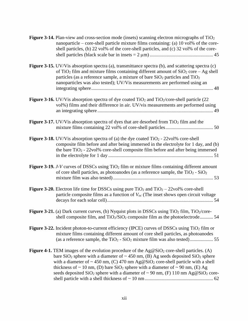
Figure 3-14. Plan-view and cross-section mode (insets) scanning electron micrographs of TiO2
nanoparticle – core-shell particle mixture films containing: (a) 10 vol% of the core-
shell particles, (b) 22 vol% of the core-shell particles, and (c) 32 vol% of the core-
shell particles (black scale bar in insets = 2 m) .................................................... 45
Figure 3-15. UV/Vis absorption spectra (a), transmittance spectra (b), and scattering spectra (c)
of TiO2 film and mixture films containing different amount of SiO2 core – Ag shell
particles (as a reference sample, a mixture of bare SiO2 particles and TiO2
nanoparticles was also tested); UV/Vis measurements are performed using an
integrating sphere .................................................................................................... 48
Figure 3-16. UV/Vis absorption spectra of dye coated TiO2 and TiO2/core-shell particle (22
vol%) films and their difference in air. UV/vis measurements are performed using
an integrating sphere ............................................................................................... 49
Figure 3-17. UV/Vis absorption spectra of dyes that are desorbed from TiO2 film and the
mixture films containing 22 vol% of core-shell particles ....................................... 50
Figure 3-18. UV/Vis absorption spectra of (a) the dye coated TiO2 - 22vol% core-shell
composite film before and after being immersed in the electrolyte for 1 day, and (b)
the bare TiO2 - 22vol% core-shell composite film before and after being immersed
in the electrolyte for 1 day ...................................................................................... 51
Figure 3-19. J-V curves of DSSCs using TiO2 film or mixture films containing different amount
of core shell particles, as photoanodes (as a reference sample, the TiO2 - SiO2
mixture film was also tested) .................................................................................. 53
Figure 3-20. Electron life time for DSSCs using pure TiO2 and TiO2 – 22vol% core-shell
particle composite films as a function of Voc (The inset shows open circuit voltage
decays for each solar cell) ....................................................................................... 54
Figure 3-21. (a) Dark current curves, (b) Nyquist plots in DSSCs using TiO2 film, TiO2/core-
shell composite film, and TiO2/SiO2 composite film as the photoelectrode ........... 54
Figure 3-22. Incident photon-to-current efficiency (IPCE) curves of DSSCs using TiO2 film or
mixture films containing different amount of core shell particles, as photoanodes
(as a reference sample, the TiO2 - SiO2 mixture film was also tested) ................... 55
Figure 4-1. TEM images of the evolution procedure of the Ag@SiO2 core-shell particles. (A)
bare SiO2 sphere with a diameter of ~ 450 nm, (B) Ag seeds deposited SiO2 sphere
with a diameter of ~ 450 nm, (C) 470 nm Ag@SiO2 core-shell particle with a shell
thickness of ~ 10 nm, (D) bare SiO2 sphere with a diameter of ~ 90 nm, (E) Ag
seeds deposited SiO2 sphere with a diameter of ~ 90 nm, (F) 110 nm Ag@SiO2 core-
shell particle with a shell thickness of ~ 10 nm ........................................................ 62
xiii
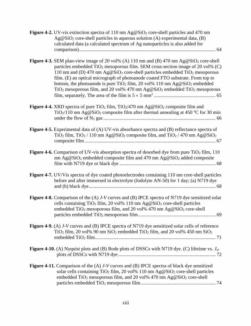
Figure 4-2. UV-vis extinction spectra of 110 nm Ag@SiO2 core-shell particles and 470 nm
Ag@SiO2 core-shell particles in aqueous solution (A) experimental data, (B)
calculated data (a calculated spectrum of Ag nanoparticles is also added for
comparison)............................................................................................................... 64
Figure 4-3. SEM plan-view image of 20 vol% (A) 110 nm and (B) 470 nm Ag@SiO2 core-shell
particles embedded TiO2 mesoporous film. SEM cross-section image of 20 vol% (C)
110 nm and (D) 470 nm Ag@SiO2 core-shell particles embedded TiO2 mesoporous
film. (E) an optical micrograph of photoanode coated FTO substrate. From top to
bottom, the photoanode is pure TiO2 film, 20 vol% 110 nm Ag@SiO2 embedded
TiO2 mesoporous film, and 20 vol% 470 nm Ag@SiO2 embedded TiO2 mesoporous
film, separately. The area of the film is 5 5 mm2 .................................................. 65
Figure 4-4. XRD spectra of pure TiO2 film, TiO2/470 nm Ag@SiO2 composite film and
TiO2/110 nm Ag@SiO2 composite film after thermal annealing at 450 oC for 30 min
under the flow of N2 gas ........................................................................................... 66
Figure 4-5. Experimental data of (A) UV-vis absorbance spectra and (B) reflectance spectra of
TiO2 film, TiO2 / 110 nm Ag@SiO2 composite film, and TiO2 / 470 nm Ag@SiO2
composite film .......................................................................................................... 67
Figure 4-6. Comparison of UV-vis absorption spectra of desorbed dye from pure TiO2 film, 110
nm Ag@SiO2 embedded composite film and 470 nm Ag@SiO2 added composite
film with N719 dye or black dye .............................................................................. 68
Figure 4-7. UV/Vis spectra of dye coated photoelectrodes containing 110 nm core-shell particles
before and after immersed in electrolyte (Iodolyte AN-50) for 1 day; (a) N719 dye
and (b) black dye ....................................................................................................... 68
Figure 4-8. Comparison of the (A) J-V curves and (B) IPCE spectra of N719 dye sensitized solar
cells containing TiO2 film, 20 vol% 110 nm Ag@SiO2 core-shell particles
embedded TiO2 mesoporous film, and 20 vol% 470 nm Ag@SiO2 core-shell
particles embedded TiO2 mesoporous film ............................................................... 69
Figure 4-9. (A) J-V curves and (B) IPCE spectra of N719 dye sensitized solar cells of reference
TiO2 film, 20 vol% 90 nm SiO2 embedded TiO2 film, and 20 vol% 450 nm SiO2
embedded TiO2 film .................................................................................................. 71
Figure 4-10. (A) Nyquist plots and (B) Bode plots of DSSCs with N719 dye. (C) lifetime vs. Jsc
plots of DSSCs with N719 dye ............................................................................... 72
Figure 4-11. Comparison of the (A) J-V curves and (B) IPCE spectra of black dye sensitized
solar cells containing TiO2 film, 20 vol% 110 nm Ag@SiO2 core-shell particles
embedded TiO2 mesoporous film, and 20 vol% 470 nm Ag@SiO2 core-shell
particles embedded TiO2 mesoporous film ............................................................. 74

xiv
Figure 5-1. (a) HRTEM images of colloidal PbS QDs with an average diameter of 6.5 nm. (b)
Optical characterization of toluene solutions of oleic acid capped PbS QDs ........... 79
Figure 5-2. Different Types of Surface Ligands Used in Nanocrystals and Nanocrystal Solids . 80
Figure 5-3. In the organic passivation route for PbS QDs, EDT substitutes the long OA ligands
and binds to Pb2+ on the surface ............................................................................... 81
Figure 5-4. (a) Scanning electron microscopy cross-section of the ITO/PbSe_QDs/metal device
stack. The metal is 20 nm Ca/100 nm Al. The scale bar represents 100 nm. (b) A
cartoon of the PbSe QDs Schottky solar device.155 (c) Proposed equilibrium band
diagram. Showing the presence of a Schottky barrier and bending in the conduction
band and valence band near the metal/PbSe QDs interface. The built-in electric field
within the depletion region of electrons and holes.156 (d) Similar band diagram of
Schottky barrier near the Al/PbS QDs interface ....................................................... 82
Figure 5-5. Current transient signals used to extract (a) the hole mobility (CELIV, 80000 V s-1
ramp rate) and (b) the electron mobility (time-of-flight, under 40 V bias). (c) Voc
decay signal (after 975 nm, 16 mW cm-2 illumination turn off) and a linear best fit
(dashed red line) used to determine the recombination-llimited lifetime. (d) Lifetime
(blue crosses, left axis) and EQE (red circles, right axis) and as a function of
illumination intensity at 975 nm ............................................................................... 84
Figure 5-6. Comparison of three QDs based photovoltaic architectures under photovoltaic
operation close to maximum Voc. Ef,n and Ef,p are the electron and hole quasi-Fermi
levels; Ec and Ev are the conduction and valence band edges; Jp,PV and Jn,PV are the
hole and electron photocurrents (and are equal at steady state); Jp,fwd is the hole
current in the forward bias direction ......................................................................... 86
Figure 5-7. Schematic diagram of a p-n junction. qVoc is the difference between the quasi-Fermi
level Fn of electrons in the n-type material and quasi-Fermi level Fp of holes in the
p-type material under illumination. Mid-gap states and shallow traps are present in
both the p- and n-type materials................................................................................ 88
Figure 5-8. (a) Energy level alignment of TiO2 and PbS QDs of different sizes. The Fermi level
is shown as a dashed line. (b) Solution absorption spectra in toluene of the three
different PbS QDs used in device fabrication. The experimental values of Voc are
shown above each excitonic peak, and the upper limit to Voc, calculated from the
difference in Fermi levels shown in panel (a) is drawn as a dashed line. (c) Cross-
section TEM of a photovoltaic device. The sample was prepared by focused-ion-
beam milling. The line plot shows the elemental distribution as determined by
energy-dispersive X-ray analysis (yellow, S; blue, Pb; green, Ti; cyan, Sn; red, O;
light blue, Au). Scale bar is 200 nm.......................................................................... 89
Figure 5-9. (a) Schematics of XPS process of 1s signal.190 (b) Fitting of O 1s spectra for air
annealed film with chemical species and corresponding atomic percentages .......... 90
xv
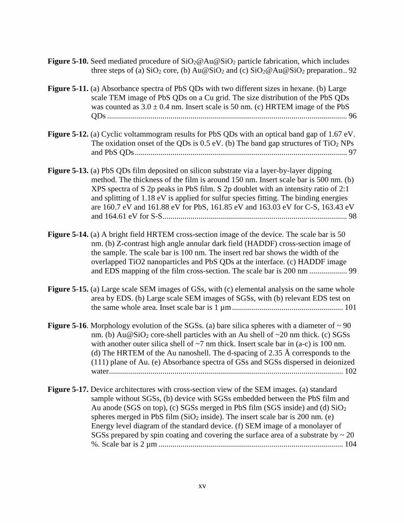
Figure 5-10. Seed mediated procedure of SiO2@Au@SiO2 particle fabrication, which includes
three steps of (a) SiO2 core, (b) Au@SiO2 and (c) SiO2@Au@SiO2 preparation .. 92
Figure 5-11. (a) Absorbance spectra of PbS QDs with two different sizes in hexane. (b) Large
scale TEM image of PbS QDs on a Cu grid. The size distribution of the PbS QDs
was counted as 3.0 ± 0.4 nm. Insert scale is 50 nm. (c) HRTEM image of the PbS
QDs ......................................................................................................................... 96
Figure 5-12. (a) Cyclic voltammogram results for PbS QDs with an optical band gap of 1.67 eV.
The oxidation onset of the QDs is 0.5 eV. (b) The band gap structures of TiO2 NPs
and PbS QDs ........................................................................................................... 97
Figure 5-13. (a) PbS QDs film deposited on silicon substrate via a layer-by-layer dipping
method. The thickness of the film is around 150 nm. Insert scale bar is 500 nm. (b)
XPS spectra of S 2p peaks in PbS film. S 2p doublet with an intensity ratio of 2:1
and splitting of 1.18 eV is applied for sulfur species fitting. The binding energies
are 160.7 eV and 161.88 eV for PbS, 161.85 eV and 163.03 eV for C-S, 163.43 eV
and 164.61 eV for S-S ............................................................................................. 98
Figure 5-14. (a) A bright field HRTEM cross-section image of the device. The scale bar is 50
nm. (b) Z-contrast high angle annular dark field (HADDF) cross-section image of
the sample. The scale bar is 100 nm. The insert red bar shows the width of the
overlapped TiO2 nanoparticles and PbS QDs at the interface. (c) HADDF image
and EDS mapping of the film cross-section. The scale bar is 200 nm ................... 99
Figure 5-15. (a) Large scale SEM images of GSs, with (c) elemental analysis on the same whole
area by EDS. (b) Large scale SEM images of SGSs, with (b) relevant EDS test on
the same whole area. Inset scale bar is 1 µm ........................................................ 101
Figure 5-16. Morphology evolution of the SGSs. (a) bare silica spheres with a diameter of ~ 90
nm. (b) Au@SiO2 core-shell particles with an Au shell of ~20 nm thick. (c) SGSs
with another outer silica shell of ~7 nm thick. Insert scale bar in (a-c) is 100 nm.
(d) The HRTEM of the Au nanoshell. The d-spacing of 2.35 Å corresponds to the
(111) plane of Au. (e) Absorbance spectra of GSs and SGSs dispersed in deionized
water ...................................................................................................................... 102
Figure 5-17. Device architectures with cross-section view of the SEM images. (a) standard
sample without SGSs, (b) device with SGSs embedded between the PbS film and
Au anode (SGS on top), (c) SGSs merged in PbS film (SGS inside) and (d) SiO2
spheres merged in PbS film (SiO2 inside). The insert scale bar is 200 nm. (e)
Energy level diagram of the standard device. (f) SEM image of a monolayer of
SGSs prepared by spin coating and covering the surface area of a substrate by ~ 20
%. Scale bar is 2 µm ............................................................................................. 104
xvi
Figure 5-18. Cross-section view and top view of the SGS_inside device. The scale bar is 500 nm
............................................................................................................................... 105
Figure 5-19. (a) J-V curve and (b) IPCE spectra of the devices including standard sample
without SGS, SGS on top, SGS inside and SiO2 spheres inside. (c) IPCE
enhancement spectra. i.e. (IPCE of device with SGS on top/IPCE of the standard
device). (d) Absorbance spectra of various tandem films: PbS/TiO2/FTO,
SGS/TiO2/FTO, SGS/PbS/TiO2/FTO, and PbS/SGS/TiO2/FTO .......................... 107
Figure 5-20. The optical constants of the PbS QDs film relative to values for bulk PbS .......... 109
Figure 5-21. (a) Schematics of the (i) 150 nm PbS QD thin film on 20 nm Au back reflector and
(ii) same structure with SGSs on the backside, (b) absorption per volume (in units
of 1/nm3) at λ = 680 nm for the two structures (the incident light is from the bottom
and hits the PbS QD layer first) ............................................................................ 111
Figure 5-22. Absorption per volume at λ = 680 nm for (a) PbS QD thin film with embedded
SGS, (b) PbS QD thin film with the curved PbS surface, and (c) PbS QD thin film
with SGS and the curved Au surface .................................................................... 112
Figure 5-23. (a) Electron lifetime of the devices measured by an open-circuit voltage decay
(OCVD) technique. (b) Comparison of the Nyquist plots of the devices with real
data (hollow dot), generated from electrochemical impedance spectroscopy (EIS)
test, and fitting data (solid line) ............................................................................ 114
Figure 6-1. (a) Absorbance spectra of the TiO2 and TiO2/SGSs_10 % composite films, as well as
the theoretical absorption coefficient spectrum of the SGSs. (b) Absorbance spectra
of the composite film after different annealing treatments. Inset shows the schematic
setup of UV annealing ............................................................................................ 117
Figure 6-2. (a) Schematic PbS heterojunction solar device structure with a MoOx hole extraction
layer.200 (b) Schematic energy diagram of interfacial layers PbS/MoOx ................ 118

xvii
PREFACE
This dissertation includes some contents published/submitted in peer reviewed journal papers,
and a list of journal papers is as following:
Chapter 3 Bo Ding, Bong Jae Lee, Mengjin Yang, Hyun Suk Jung and Jung-Kun Lee,
Surface-Plasmon Assisted Energy Conversion in Dye-Sensitized Solar Cells, Adv. Energy
Mater. 2011, 1, (3), 415-421.
Chapter 4. Bo Ding, Mengjin Yang, Bong Jae Lee, and Jung-Kun Lee, Tunable Surface
Plasmons of Dielectric Core-Metal Shell Particles for Dye Sensitized Solar Cells, RSC Advances
2013, 3, (25), 9690-9697.
During my PhD study, I got a lot of help and encouragement. I would glad to express my
appreciation and acknowledgement during this exciting journey.
First and foremost, I would like to thank my advisor Professor Jung-Kun Lee for his kind
guidance during my PhD study. His passionate, diligent, critic-thinking influences my research
tremendously. I am impressed by his knowledge, strong logic and creativity. Without his
mentoring, it is impossible for me to survive and finish my PhD study.
Also, thanks a lot to the other committee members, Professor Paul W. Leu, Professor
John A. Barnard, Professor Ian Nettleship and Professor Guofeng Wang. Their kindness and
pertinent advice always broaden my horizons in research. Here, I especially appreciate the great
help from Professor Paul W. Leu, Professor David Waldeck and Professor Bong Jae Lee, who

xviii
are the collaborators with our group. Professor Leu is very professional in nanophotonics
simulation and helps me a lot in explaining and proving the plasmon effect in PbS based solar
cells by theoretical calculations. Professor Waldeck is a very kind and generous expert in
interfacial charge transfer and nanophotonics, and shares brilliant ideas and some test tools for
my research. Professor Bong Jae Lee is a knowledgeable researcher and contributed a lot at the
beginning of my study in plasmon assisted DSSCs.
I am very lucky to have great members in our dynamic group: You-Hwan Son, Mengjin
Yang, Po-shun Huang, Youngsoo Jung and Salim Caliskan. They are smart and diligent.
Particularly grateful to Mengjin, who helped me a lot either in research or daily life when I
joined this group. Also, he setup the OCVD and SLIM-PCV systems for electron lifetime
measurement, which brings convenience to solar device characterization.
Thanks to my other colleagues and friends, who give selfless collaboration and
contribution to my work: Matt Barry, Yang He, Xiahan Sang, Feng Zhou, Zhongfan Zhang,
Gautam Reddy, and especially Tongchuan Gao and Yang Wang, who are very smart and patient
collaborators and friends. With their assistance, my research became much easier and more
productive.
Moreover, thanks to Materials Science Characterization Lab and Nano-Scale Fabrication
and Characterization facility, and their staffs: Albert Stewart, who is always the best staff I ever
met, Cole Van Ormer, Shusheng Tan, Matthew France and Joel Gillespie.
Finally, I want to express my gratitude to my parents, who give me life and support me
unconditionally and constantly.
1
1.0 INTRODUCTION
Surface plasmons (SPs) are a result of electromagnetic radiation induced coherent oscillations of
free electrons on a metal.1, 2 Their unique properties have attracted much attention due to its
practical applications, including light guiding and manipulation at the nanoscale, high resolution
optical imaging below the diffraction limit, as well as biodetection at the single molecule level.
This diverse and rapidly growing field of research on such optical-metallic interactions is well
known as ‘plasmonics’.3-5
The first scientific study of surface plasmons dates back to 1902 when Prof. Robert W.
Wood observed unexplained phenonema in optical reflection test on metallic gratings.6, 7 In 1908,
Gustav Mie developed his famous and widely used Mie theory, a rigorous analytical solution of
Maxwell’s equations for light scattering by spherical particles.8 In 1957, Rufus Ritchie found
that plasmon modes could exist near the surface of metal, which represents the first theoretical
description of surface plasmons.9 A main breakthrough was made in 1968 by Andreas Otto et
al.10, 11 who designed methods for optical excitation of surface plasmons on metallic films,
facilitating experiments on surface plasmons to many other researchers.
Surface plasmon resonances (SPRs) usually can be divided into two kinds: (i)
propagating surface plasmon polaritons (SPPs) and (ii) nonpropagating localized surface
plasmon resonances (LSPRs).12 The SPP, firstly introduced by Stephen Cunningham et al. in
1974,13 can be excited on the thin metallic film by using prism or grating couplers. LSPR is

2
excited by ordinary or nonevanescent propagating light, and intimately coupled to such light as
well. In other words, it is nonpropagating plasmon excitations that can be resonantly excited on
metal nanoparticles (NPs) or in metal films. These two types of SPRs propagate along the metal
film with an associated electric field which decays normally and exponentially from the metal-
dielectric interface.14 In addition, the plasmon resonance peak can be shifted by changing the
refractive index above the metal.
1.0.1 Plasmonic Metal Nanoparticles
Nobel metal NPs, especially gold (Au) and silver (Ag), are frequently studied due to their strong
SPRs in the visible wavelength range.15 The incident photon frequency can be resonant with
collective oscillation of the free electrons in the metal NPs, causing LSPRs. The free electrons in
the particle will all move in phase under plane-wave excitation, leading to a buildup polarization
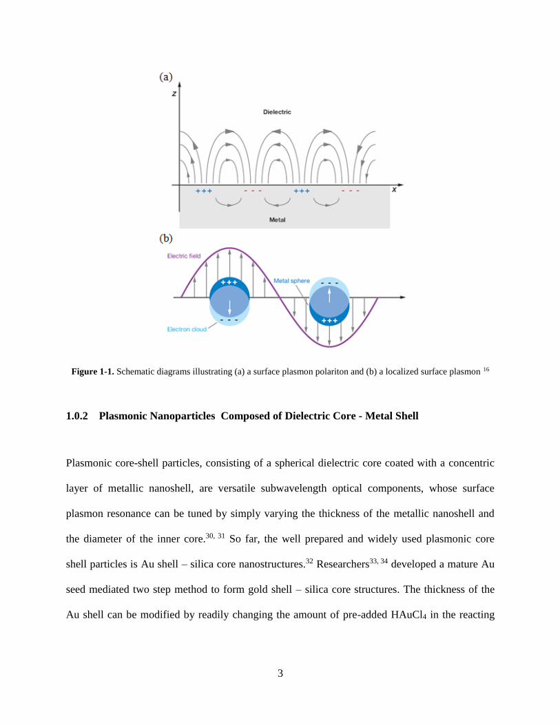
charges on the surface of the particle as a restoring force (Fig. 1-1).16 This restoring force will
allow a resonance to occur at a specific frequency named particle dipole plasmon frequency. In
the meanwhile, a dipolar field is produced outside, resulting in an intensified surface plasmon
absorption band, and enhanced near-field in the vicinity of the particle surface. The absorption
bandwidth and the position and intensity of the maximum absorption peak is determined by the
material, as well as its morphology and dimension.17
Thanks to the talented chemist and physicist, in the past decades, various synthetic
methodologies for generating nanostructures with well controlled sizes and shapes from a variety
of materials were set up.18-21 By this way, plasmonic metal nanostructures with different
morphologies and dimensions, like spheres,22 cubes,23, 24 rods25, 26 and plates27 were designed,
merging the ability to accurately control and tailor their optical properties.28, 29
3
Figure 1-1. Schematic diagrams illustrating (a) a surface plasmon polariton and (b) a localized surface plasmon 16
1.0.2 Plasmonic Nanoparticles Composed of Dielectric Core - Metal Shell
Plasmonic core-shell particles, consisting of a spherical dielectric core coated with a concentric
layer of metallic nanoshell, are versatile subwavelength optical components, whose surface
plasmon resonance can be tuned by simply varying the thickness of the metallic nanoshell and
the diameter of the inner core.30, 31 So far, the well prepared and widely used plasmonic core
shell particles is Au shell – silica core nanostructures.32 Researchers33, 34 developed a mature Au
seed mediated two step method to form gold shell – silica core structures. The thickness of the
Au shell can be modified by readily changing the amount of pre-added HAuCl4 in the reacting
4
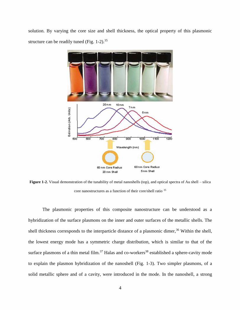
solution. By varying the core size and shell thickness, the optical property of this plasmonic
structure can be readily tuned (Fig. 1-2).35
Figure 1-2. Visual demonstration of the tunability of metal nanoshells (top), and optical spectra of Au shell – silica
core nanostructures as a function of their core/shell ratio 35
The plasmonic properties of this composite nanostructure can be understood as a
hybridization of the surface plasmons on the inner and outer surfaces of the metallic shells. The
shell thickness corresponds to the interparticle distance of a plasmonic dimer,36 Within the shell,
the lowest energy mode has a symmetric charge distribution, which is similar to that of the
surface plasmons of a thin metal film.37 Halas and co-workers38 established a sphere-cavity mode
to explain the plasmon hybridization of the nanoshell (Fig. 1-3). Two simpler plasmons, of a
solid metallic sphere and of a cavity, were introduced in the mode. In the nanoshell, a strong
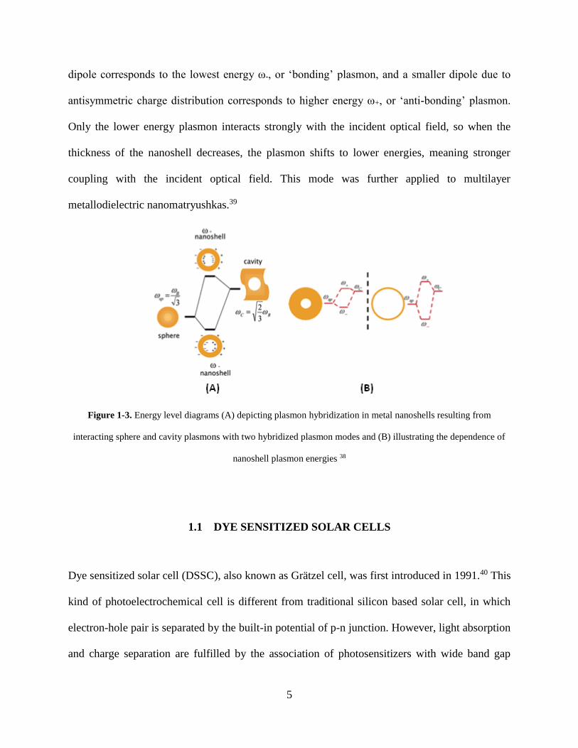
5
dipole corresponds to the lowest energy ω-, or ‘bonding’ plasmon, and a smaller dipole due to
antisymmetric charge distribution corresponds to higher energy ω+, or ‘anti-bonding’ plasmon.
Only the lower energy plasmon interacts strongly with the incident optical field, so when the
thickness of the nanoshell decreases, the plasmon shifts to lower energies, meaning stronger
coupling with the incident optical field. This mode was further applied to multilayer
metallodielectric nanomatryushkas.39
Figure 1-3. Energy level diagrams (A) depicting plasmon hybridization in metal nanoshells resulting from
interacting sphere and cavity plasmons with two hybridized plasmon modes and (B) illustrating the dependence of
nanoshell plasmon energies 38
1.1 DYE SENSITIZED SOLAR CELLS
Dye sensitized solar cell (DSSC), also known as Grätzel cell, was first introduced in 1991.40 This
kind of photoelectrochemical cell is different from traditional silicon based solar cell, in which
electron-hole pair is separated by the built-in potential of p-n junction. However, light absorption
and charge separation are fulfilled by the association of photosensitizers with wide band gap
6
semiconductors. The theoretical efficiency of the DSSC is as high as 19.6 % and very compatible
to that of commercial silicon based solar cell.41 Furthermore, several other advantages, like low
fabrication cost, easy scale-up using flexible substrate, and good performance under
weak/diffuse light, make DSSC to be a promising alternative to high cost and polluted silicon
industry in the future. During the last two decades, DSSCs have been greatly studied, leading to
a great increase of the cell performance. So far, the best efficiency of the DSSCs in the lab scale
has already surpassed 11 %.42, 43 And the manufacturers, like Sharp and Sony, announce that the
submodule efficiencies have been reaching up to 10.4 % and 9.2 % separately,44 which means a
pioneer footstep to commercial market.
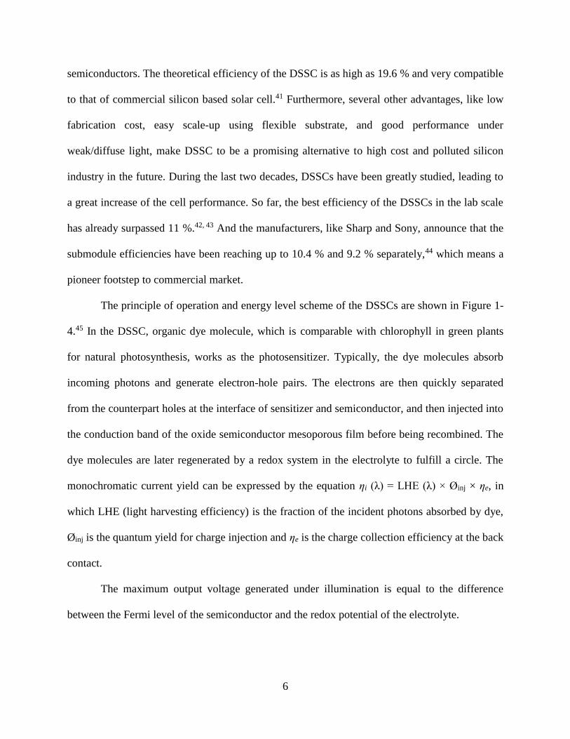
The principle of operation and energy level scheme of the DSSCs are shown in Figure 1-
4.45 In the DSSC, organic dye molecule, which is comparable with chlorophyll in green plants
for natural photosynthesis, works as the photosensitizer. Typically, the dye molecules absorb
incoming photons and generate electron-hole pairs. The electrons are then quickly separated
from the counterpart holes at the interface of sensitizer and semiconductor, and then injected into
the conduction band of the oxide semiconductor mesoporous film before being recombined. The
dye molecules are later regenerated by a redox system in the electrolyte to fulfill a circle. The
monochromatic current yield can be expressed by the equation ηi (λ) = LHE (λ) × Øinj × ηe, in
which LHE (light harvesting efficiency) is the fraction of the incident photons absorbed by dye,
Øinj is the quantum yield for charge injection and ηe is the charge collection efficiency at the back
contact.
The maximum output voltage generated under illumination is equal to the difference
between the Fermi level of the semiconductor and the redox potential of the electrolyte.
7
Figure 1-4. DSSC structure and energy band alignment superposition diagram 45
The photosensitizer plays a critical role in generating electron-hole pairs in the DSSC.
Although quantum dots such as CdSe46 and PbSe47 were employed as the sensitizing materials
recently, organic dyes containing polypyridyl complex of ruthenium (Ru) are widely used as the
photosensitizer due to its high efficiency and long term stability.
The photoanode acts as electron transport path, light path, and dye anchoring scaffold.
The use of TiO2 nanocrystals with high surface area in DSSCs matches the lowest unoccupied
molecular orbital (LUMO) and the conduction level of the anodes and improves the charge
transfer properties, leading to high energy conversion efficiency.48
Electrolyte works as an electron-transfer mediator which regenerates the dye sensitizer
from its oxidized state. So far, liquid electrolytes are mostly common used because of the
effective catalytic reaction at the counter electrode and its fast ionic diffusion. Although some
new redox systems, such as Br- /Br3-,49 cobalt (II/III),50 disulfide / thiolate,51 and ferrocene /
ferrocenium52 redox mediator, have been investigated, they are still unrivaled to conventional I- /
8
I3- electrolyte, which keeps the record efficiency of 12 %,42 for its very low recombination
kinetic between electrons in TiO2 and triiodide.53 However, liquid volatile electrolyte will cause
leaking problem under thermal and light-soaking dual stress, and evaporation of the organic
solvent drops the long-term stability of the cell.54 Recently, solvent-free ionic liquid electrolyte,55
solid-state electrolyte56, 57 and quasi-solid electrolyte58, 59 have been explored to overcome the
weakness of the liquid electrolyte and enhance the long stability of the DSSC.
1.2 APPLICATION OF THE PLASMONIC STRUCTURES
1.2.1 Photovoltaic
Photovoltaics (PVs), conversion of solar energy to electricity, has been growing rapidly and
attracting much attention of researchers and government energy agencies, due to the urgent
global demand for renewable energy sources. In order to lower the production cost and make
large scale PV panel, thin film solar cell has become the main trend,60 and convenient roll-to-roll
technique is applied for flexible module fabrication.61 In addition, thin film with thickness
smaller than the carrier diffusion length (Ln) would greatly suppress the bulk recombination.
Apart from above mentioned DSSC, various semiconductors have been used for thin film solar
cell, such as monocrystalline and polycrystalline silicons, GaAs, CdTe and CuInSe2, as well as
organic semiconductors.62 One major limitation of the thin film solar cell is that the absorbance
of near-bandgap light is suppressed due to small light path length. However, traditional light
trapping method, using pyramidal surface texture,63 is not proper to thin film solar cell, since the
9
surface roughness would surpass the film thickness, and minority carrier recombination is
increased due to larger surface area and junction regions.
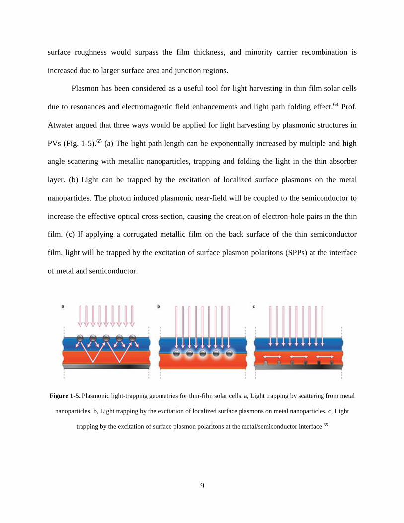
Plasmon has been considered as a useful tool for light harvesting in thin film solar cells
due to resonances and electromagnetic field enhancements and light path folding effect.64 Prof.
Atwater argued that three ways would be applied for light harvesting by plasmonic structures in
PVs (Fig. 1-5).65 (a) The light path length can be exponentially increased by multiple and high
angle scattering with metallic nanoparticles, trapping and folding the light in the thin absorber
layer. (b) Light can be trapped by the excitation of localized surface plasmons on the metal
nanoparticles. The photon induced plasmonic near-field will be coupled to the semiconductor to
increase the effective optical cross-section, causing the creation of electron-hole pairs in the thin
film. (c) If applying a corrugated metallic film on the back surface of the thin semiconductor
film, light will be trapped by the excitation of surface plasmon polaritons (SPPs) at the interface
of metal and semiconductor.
Figure 1-5. Plasmonic light-trapping geometries for thin-film solar cells. a, Light trapping by scattering from metal
nanoparticles. b, Light trapping by the excitation of localized surface plasmons on metal nanoparticles. c, Light
trapping by the excitation of surface plasmon polaritons at the metal/semiconductor interface 65
10
Due to the unique plamonic properties, metallic nanostructures have been largely
employed in thin film PVs with various methods, resulting in an improved photocurrent and
energy conversion efficiency. Such as embedding metal nanoparticles in single-crystalline Si,66
contacting Ag film in organic solar cells,67 and mixing small metal clusters in DSSCs.68
1.2.2 Other Applications
1.2.2.1 Surface-Enhanced Raman Spectroscopy
Raman spectroscopy is a very useful tool for capturing molecule-specific data, since the Raman
signal contains detailed information of the molecule vibration. However, it lacks the intrinsic
sensitivity required for high output detection due to weak signal intensity. To address this
problem, plasmonic nanostructures were employed for signal enhancement. A million-fold
enhancement can be realized attributing to excitation of surface plasmons of the metallic
substrate.69 The strong local fields at the metal surface coupled with its plasmon resonance are
responsible for this dramatic enhancement. This high sensitivity of surface-enhanced Raman
scattering (SERS) can even be applied to much complex environment, like inside live cells.70
Researchers later found that aggregated Au and Ag clusters or films had larger enhancement
effect than individual metal nanoparticle, for the high-field intensities are associated with dimer
plasmons or junctions between neighbor nanoparticles.71
SERS in near-infrared region has become a very attracting research area, since unwanted
background fluorescence from molecules is dramatically suppressed when probing chemical
complex environments, and Raman scattering signal is much weaker in infrared region than that
of visible wavelengths. In order to solve this problem, metal nanoshells are designed, and the
11
plasmon resonance is tuned near the pump laser wavelength via changing the geometry of the
core-shell nanostructures.72 Three Stokes modes were applied to understand the nanoshell
accompanied SERS. And the significant enhancement was found when absorption of the Stokes
emission is minimized.73
1.2.2.2 Photoacoustic Signal Nanoamplifiers
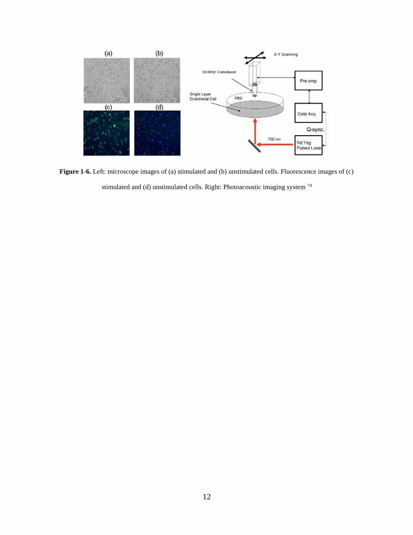
Photoacoustic is the effect of absorbed light on matter by means of acoustic detection. This
phenomenon was firstly discovered by Alexander Graham Bell in 1880 that is after exposing to
sunlight, a thin disc produced sound in response. Photoacoustic was originally controlled by an
energy conversion procedure from light to local heating. Later on, photoacoustic imaging
technology was developed by applying a laser pulse on an object, and photogenerated heat was
expanded and captured by a remote sensor as acoustic wave. The distribution of optical
absorption within such object can be depicted as acoustic field.74 The contrast of photoacoustic
imaging depends upon the optoacoustic efficiency, which is determined by the number of
absorbed incident photons for heat generation and the speed of heat release during thermal
expansion and wave generation.75 Au nanostructures have usually been chosen as contrast and
therapeutic agents due to their excellent plasmonic effect.76 The photoacoustic contrast can be
optimized by maximizing the optical absorption cross section of the metallic nanostructures. So
far, Au nanorods,77 nanocages78 and nanoshells79 have been successfully applied as the
photoacoustic amplifier. The photoacoustic imaging system and typical image are shown in
Figure 1-6.
12
Figure 1-6. Left: microscope images of (a) stimulated and (b) unstimulated cells. Fluorescence images of (c)
stimulated and (d) unstimulated cells. Right: Photoacoustic imaging system 74

13
1.3 CHALLENGES OF METALLIC CORE-SHELL PARTICLES
As described above, metallic nanoshell - silica core structures have unique properties that
advance current technology in the fields of photovoltaics, SERS, and photoacoustic imaging.
However, several issues still have to be addressed to maximize the potential of plasmonic core-
shell structures.
First of all, although Au nanoshell - silica core (Au@SiO2) structures have been well
prepared and widely used so far, another noble element Ag has been less considered as a
plasmonic core-shell structure, due to lacking of effective method to synthesize complete Ag
nanoshell – silica core (Ag@SiO2) particles. Ag nanoshell owns some unique optical properties,
like strong scattering spectrum and tunable blue shifted extinction (absorption + scattering)
spectrum. In addition, Ag has stronger resonance strength80 and much cheaper cost than Au, so
there is no reason to hide it from shining. Several methods, like sonication,81 seed mediation82
and electroless plating,83, 84 have been explored for Ag@SiO2 preparation, however, only Ag
nanoparticles or nanoclusters have been achieved for surface decorating instead of forming
complete Ag nanoshells. Therefore, it is required to develop a new way to form complete Ag
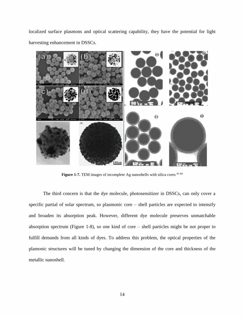
nanoshell on silica core. Figure 1-7 shows the TEM images of the incomplete Ag nanoshell –
silica core particles prepared by previous trials.
Second issue is that no metallic shell - dielectric core plasmonic structures have been
applied in DSSCs. Although plasmonic nanoparticles have been widely used in various PVs as
we discussed before, however, only until very recently, metal nanoparticles have been
investigated in DSSCs.85, 86 Since plasmonic core – shell particles are considered to have strong
14
localized surface plasmons and optical scattering capability, they have the potential for light
harvesting enhancement in DSSCs.
Figure 1-7. TEM images of incomplete Ag nanoshells with silica cores 81-84
The third concern is that the dye molecule, photosensitizer in DSSCs, can only cover a
specific partial of solar spectrum, so plasmonic core – shell particles are expected to intensify
and broaden its absorption peak. However, different dye molecule preserves unmatchable
absorption spectrum (Figure 1-8), so one kind of core – shell particles might be not proper to
fulfill demands from all kinds of dyes. To address this problem, the optical properties of the
plamonic structures will be tuned by changing the dimension of the core and thickness of the
metallic nanoshell.

15
Figure 1-8. (Top) Molecule structures of N719 and black dyes. (Bottom left) Absorption spectra of N719 and black
dyes. (Bottom right) Prototype DSSCs employing N719 and black dyes

16
2.0 OPTICAL SIMULATION OF PLASMONIC STRUCTURES
2.1 MOTIVATION
Surface plasmons can be successfully described by macroscopic electromagnetic theory, and the
most classical one is Maxwell’s equations.87 Although, strictly speaking, this theory is applicable
in a macroscopic sense, however, so far, it has been well extrapolated to the region of nanometer
scale.88 The Maxwell’s equations describe how electric charges and currents influence electric
and magnetic fields. Typically, four equations are included to describe the electromagnetic field
at a time t and any point r in a medium characterized by their bulk dielectric constant ε (r, t) and
magnetic permeability µ (r, t). Conceptually, Gauss’s law and Gauss’s law for magnetism
describe how charges emanate fields, and Ampere’s law and Faraday’s law depict how fields
circulate around relevant sources. The differential form of the equations is defined below, in
which E is the electric field, the charge density, B the magnetic induction, H the magnetic
field, J the current density, and D the displacement.
(Gauss’s Law) (1.1)
(Gauss’s Law for Magnetism) (1.2)
17
(Ampere’s Law) (1.3)
(Faraday’s Law) (1.4)
Above classical Maxwell’s equations are not sufficient in themselves, and constitutive
relations are needed as well. These relations have the form as follows where P is the electric
polarization, M the magnetization, σ the conductivity. In addition, µ and χ are the permeability
and electric susceptibility of the medium separately; and are the permittivity and
permeability of the free space individually.
(1.5)
(1.6)
σE (1.7)
µH (1.8)
To solve the optical scattering problem, two parameters have to be considered: d, the
physical size of the scattering object and λ, the wavelength of electromagnetic waves. For one
extreme case when d >> λ, the problem is readily solved without involving Maxwell’s equations.
With respect to another limiting case when d << λ, the solution in the quasistatic limit is obtained
by invoking Laplace’s equation. However, the problem is further more complicated when d ~ λ.
In this case, many numerical methods have been developed to fulfill the requirement, such as
Green dyadic method (GDM),89 discrete dipole approximation (DDA),90-92 finite-difference
frequency-domain method,93 and finite-difference time-domain (FDTD).94 In particular, to obtain

18
a FDTD solution of Maxwell’s equation, a computational domain is established first to describe
the corresponding physical region in the sample, and every point within the computational
domain needs to be processed to describe the electric or magnetic field around the whole region.
The advantage of these numerical methods is that it can be applied to objects with arbitrary
geometries. However, these methods are based on discretization of the fields on a numerical grid,
and a very fine grid resolution is necessary at the metal-dielectric interface to resolve the local
fields adequately. As a result, more coding complexity leads to less calculation efficiency.
Another way is to use analytical method, e.g. Mie theory. Based on this theory, the
incident plane wave and the scattering field are expanded into radiating spherical vector wave
functions. On the other hand, the internal field is expanded into regular spherical vector wave
functions. Finally, the expansion coefficients of the scattered field can be calculated by applying
the boundary condition on the spherical surface.95 Although this method, in principle, can only
be applied to objects with specific shapes, such as planar geometries, spheres and cylinders, to
some extent, it is still applicable to nonspherical particles.15 In sum, the Mie theory is far more
eligible to depict and calculate the optical properties of plasmonic nanoparticles and core-shell
structures in most cases.
2.2 SIMULATION OF PLASMONIC CORE-SHELL PARTICLES
2.2.1 Formulas for Optical Simulation of Silver Nanoparticles
Based on the excellent descriptions of Mie Scattering by Bohren and Huffman,15 Mie
calculations are realized by applying formulas below in MATLAB. For simulation of

19
homogeneous spheres, the key parameters are the Mie coefficients an, bn, cn and dn, which are
defined by equation 4.1-4.4. The amplitude of the scattered field can be computed from
parameter an and bn, and internal field from cn and dn.
(4.1)
(4.2)
(4.3)
(4.4)
In above equations, m is the refractive index of the sphere relative to the ambient
medium; is the average radius of the spherical particles; x, the production of k and , is the size
parameter; k, which is equal to 2π/λ, is the wave number of the electromagnetic wave; λ is the
corresponding wavelength. In addition, is the ratio of the magnetic permeability of the particle
to that of the ambient medium. The spherical Bessel functions, and are involved in
Mie coefficients calculation. can be obtained by defining
(4.5)
The primes mean derivatives, which following from the spherical Bessel functions
themselves
20
(4.6)
(4.7)
The relationships between Bessel and spherical Bessel functions are expressed as
(4.8)
(4.9)
where Jn and Yn are Bessel functions of the first and second kind. The recurrence formula
is defined as
(4.10)
and for n = 0 and 1, we have initial functions
; (4.11)
; (4.12)
The optical efficiencies Qi, which describe the interaction of radiation with a scattering
sphere, can be calculated by the cross section σi and geometrical particle cross section πa2,
shown as
(4.13)
Since extinction is equal to the summation of absorption and scattering, energy
conservation deduces the following expression
21
(4.14)
where Qsca is obtained from the integration of the scattered power on all directions, and
Qsca can be deduced from forward-scattering theorem, as
(4.15)
(4.16)
2.2.2 Formulas for Optical Simulation of Ag@SiO2 Nanostructures
For silver nanoshell - silica core particles, Mie coefficients an and bn are sufficient enough to
compute cross sections and scattering diagrams. The corresponding formulas are shown as
(4.17)
(4.18)
(4.19)
(4.20)
(4.21)
(4.22)
22
(4.23)
where a is the kernel radius and b is the outer radius, and m1 and m2 are the
refractive index of the inner core and outer shell, separately. Size parameters of the model
are x = ka and y = kb. , and are called Riccati-Bessel functions and can
be expressed as
(4.24)
(4.25)
(4.26)
The logarithmic derivative Dn is given by
(4.27)
The optical efficiencies Qi of the metallic shell – dielectric core structures can be derived
from the same functions (4.14 - 4.16) metioned before.
2.2.3 Results and Discussions
The absorption and scattering efficiencies were calculated for Ag nanoparticle (d=10 nm), SiO2
particle (d=320 nm), and Ag nanoshell with SiO2 core (d=340 nm) and Ag film (thickness = 10
nm). In the calculation, the Mie scattering coefficients of the core-shell particles were calculated
in two different ways. In the first case, it is assumed that the Ag film is a collection of individual
Ag nanoparticles on a SiO2 core and there is no interaction between Ag nanoparticles. In the
23
second case, the Ag layer was treated in a way similar to multilayer thin films.96 Here, the
dielectric function of Ag was calculated using the Drude critical point model, and the refractive
index of the surrounding medium was approximated as 2.37 by considering the mixed phases in
the TiO2 - core-shell mixed films.94
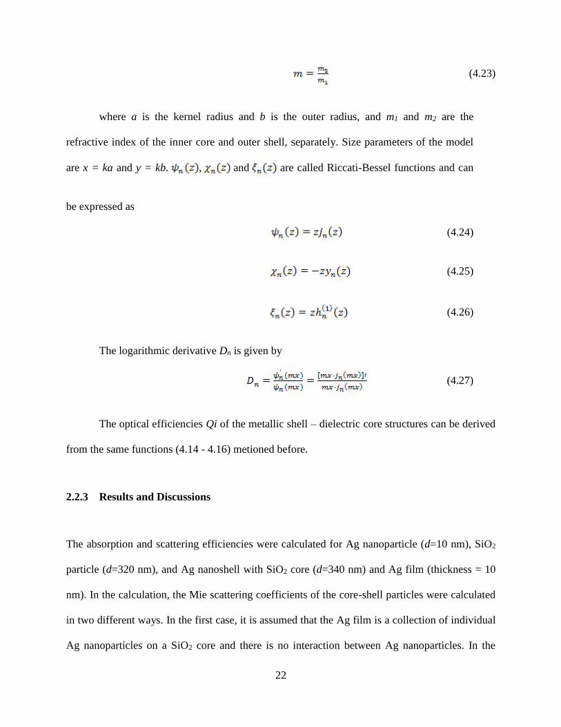
Figure 2-1 shows two different results for the absorption efficiency (i.e., absorption cross
section divided by cross sectional area) of the core-shell particles. The absorption efficiency of
Ag nanoparticles (10 nm) dramatically increases by almost two orders of magnitude near the
surface plasmon resonance wavelength of 556 nm. On the assumption that the Ag layer is a
perfect film, the calculated absorption efficiency does not exhibit the plasmonic resonance in the
visible range. The scattering efficiency (i.e., scattering cross section divided by the cross
sectional area) of the core-shell particles is also plotted in Figure 2-1b. To examine the effect of
SiO2 cores, the scattering efficiency of SiO2 particles with d = 320 nm was also calculated. In the
case of Ag nanoparticles, the calculated scattering efficiency of Ag nanoparticles also displays a
peak near the surface plasmon resonance. However, the assumption of the Ag film leads to
monotonic increase in the calculated scattering efficiency with increasing wavelength of the
incident light.
The tuning effect of the silica core – silver shell particles is shown in the simulated UV-
vis spectra by changing the size of the silica cores. Here, the silver shell is set to be 10 nm, and
two sizes of silica cores (d= 90 nm or 450 nm) are chosen to illustrate the size effect.
24
Figure 2-1. Calculated absorption efficiency (a) and scattering efficiency (b) of core-shell particles using two
different models (agglomerated Ag nanoparticles and Ag thin film) showing the nature of Ag layer (the scattering
efficiency of SiO2 particles is also calculated as a reference)
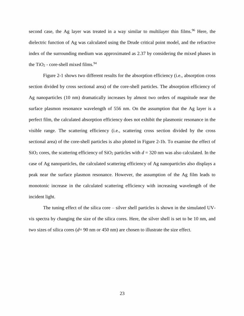
Figure 2-2 shows the extinction (absorption + scattering) spectra of Ag nanoparticle
(d=10 nm) and silica core – silver shell particles dispersed in water. Comparing with the strong
plasmonic extinction peak at 410 nm for Ag nanoparticles, plasmon peak found near 650 nm
corresponds to the Ag nanoshell with the core-shell diameter of 110 nm (Fig. 2-2a) and near 750
nm for the Ag nanoshell with the core-shell diameter of 470nm (Fig. 2-2b). The extinction of
light at red and infrared regime results from the absorption and scattering by Ag nanoshells. Its
dependence on the size clearly indicates that the wavelength of the coupled plasmon mode in
core-shell particles can be controlled by simply changing the size of the core. An increase in the
extinction in the longer wavelength is the unique plasmonic behavior of the core-shell particles,
which is explained by a hybridization model.
25
Figure 2-2. UV-vis extinction spectra of theoretical data calculated by Mie scattering approach. (a) 110 nm
Ag@SiO2 core-shell particles in aqueous solution. (b) 470 nm Ag@SiO2 core-shell particles in aqueous solution
Simulated light absorption and scattering properties of the Ag nanoparticles and core-
shell particles, which are dispersed in TiO2 matrix, are shown in Figure 2-3. Since the refractive
index of TiO2 (n=2.37) surrounding the core-shell particles is larger than water, the peaks of the
spectra shift to longer wavelength. It indicates that although the strength of absorption peak for
core-shell particles is a little weaker than that of Ag nanoparticles, the scattering efficiency is
much higher for core-shell particles.
26
Figure 2-3. Theoretically calculated (a) UV-vis absorption efficiency and (b) reflection efficiency of Ag NPs with a
diameter of 10 nm in TiO2 matrix, 10 nm thick Ag shell of 110 nm Ag@SiO2 in TiO2 matrix, and 10 nm thick Ag
shell of 470 nm Ag@SiO2 in TiO2 matrix
27
3.0 SURFACE-PLASMON ASSISTED ENERGY CONVERSION IN DSSC
3.1 BACKGROUND
3.1.1 Motivation
While DSSCs have several advantages that potentially offer an alternative to currently dominant
Si-based photovoltaics, there are still problems that need to be solved to make DSSCs as efficient
as other semiconductor-based photovoltaics. In particular, a single type of a dye material used in
DSSCs cannot absorb a full range of the solar spectrum due to the mismatch between the solar
spectrum and the light absorption spectrum of dyes.97-99 Currently, the dyes of DSSCs absorb
only part of the solar spectrum and the LHE of DSSCs is not uniformly high even in the visible
range of the solar spectrum.
To address this issue, we incorporate plasmonic nanostructures in DSSCs to control the
passage of photons. When both the energy and momentum of the incident light match those of
the plasmons, the incident light can be coupled to the plasmons. This coupling amplifies local
field intensity in the vicinity of nanostructures and enhances absorption and scattering cross-
sections.100 Recently, localized plasmons have attracted considerable attention as a promising
tool that can enhance the energy conversion efficiency of PVs. Nakayama et al., demonstrated
that high aspect-ratio Ag nanoparticles grown on the surface of optically thin GaAs solar cells
28
scattered the incident light and increased the short circuit current density of GaAs solar cells by 8
%.101 The effect of the surface plasmons on enhanced light absorption was also proved in organic
photovoltaics. Morfa et al., added a Ag nanoparticles layer into a photoactive layer in the
herterojunction photovoltaics.102 An improvement factor of 1.7 was achieved by increasing the
optical absorption and output current at long wavelengths. Similarly, Kim et al., have
systematically investigated the enhanced absorption of the organic layer due to the presence of
Ag nanoparticles.103 By incorporating plasmonic Ag nanoparticles on the surface of the ITO
electrodes, the overall energy conversion efficiency of the organic photovoltaics was increased
from 3.05% to 3.69%. The increase in the energy conversion efficiency is traced to surface
plasmon coupled light absorption, which can increase the optical cross section of the thin organic
layer. The surface plasmon effect of metal nanoparticles has been also studied in DSSCs. When
flat TiO2 films were sensitized by a combination of dye molecules and arrays of nanofabricated
elliptical gold disks, the charge carrier generation rate of the dyes increased. Standridge, et al,
used atomic layer deposition (ALD) to conformably coat arrays of silver nanoparticles with a
very thin layer of TiO2 and demonstrated plasmon enhanced photocurrent.104 In addition, Ag
nanoparticles were added to TiO2 films to increase the efficiency of DSSCs through plasmon
resonance.105, 106 In these studies, Ag nanoparticles were employed to increase the scattering of
the TiO2 films or form a photonic band gap with the TiO2 films.
In this study, we explore the influence of dielectric core - metallic nanoshell particles on
solar energy conversion in DSSCs. Because the optical resonances and the near electro-magnetic
field response can be tuned by changing the dimension of the core and shell components, the
dielectric core - metallic nanoshell particles have great potential for optoelectronic and
biomedical applications. Here, the structure of the core-shell particles is designed to arouse the
29
coupling of the surface plasmons with visible light. This coupling is expected to increase the
absorption and scattering of the light in the photoelectrodes, which contributes to enhancing the
energy conversion efficiency of the DSSCs. The new core-shell particles were distributed in
TiO2 films so that the entire photoelectrode was uniformly exposed to the plasmonic effect of the
core-shell particles. The advantage of particulate nanostructures is that they excite localized
surface plasmons regardless of the incidence geometry and polarization states of incoming light.
In newly designed DSSCs, we systematically explore the role of localized surface plasmons on
the light absorption, scattering, and energy conversion efficiency using spectroscopic and
electrochemical characterization techniques.
3.1.2 Electron Lifetime Measurement
It is important to measure the photogenerated electron lifetime in the solar cell, since the
electron-transfer kinetics play a main role in determining the conversion efficiency of the device.
So far, two methods have been mainly used in electron lifetime characterization, including open
circuit voltage decay (OCVD)107, 108 and stepped light-induced transient measurements of
photocurrent and photovoltage (SLIM-PCV).109, 110
OCVD is a powerful and simple tool to measure the electron lifetime of the DSSCs as a
function of the photovoltage (Voc). This method consists of turning off the illumination in a
steady state and monitoring the subsequent photovoltage decay.108 It provides a continuous
reading of the lifetime change against the Voc, and the data treatment based on the carrier
recombination mechanisms is quite simple. Figure 3-1 shows the measurement setup.
Monichromatic laser beam with an instant turning off at a steady state is generated from a laser
diode (λ=660 nm) which is controlled by a function generator (Agilent 33220A). A voltage

30
decay from the steady state is monitored by a digital storage oscilloscope (Tektronix,
TDS2024B) that is synchronized with the function generator.
Figure 3-1. Setup of OCVD measurement
The electron lifetime is theoretically derived from a general recombination rate, which
involves a higher reaction order electron transportation mediated by internal trapping and de-
trapping processes. For a common nonlinear case, the electron lifetime is given by the reciprocal
of the derivative of the decay curve normalized by the thermal voltage107:
(3-1)
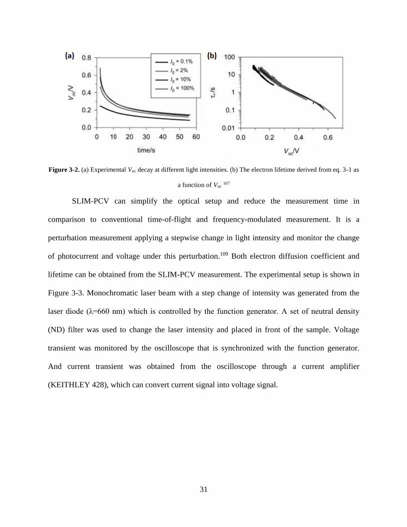
Typical results shown in Figure 3-2 consist of OCVD decay curves at different light
intensities and relevant electron lifetime values obtained from eq. 3-1 as a function of Voc.
31
Figure 3-2. (a) Experimental Voc decay at different light intensities. (b) The electron lifetime derived from eq. 3-1 as
a function of Voc 107
SLIM-PCV can simplify the optical setup and reduce the measurement time in
comparison to conventional time-of-flight and frequency-modulated measurement. It is a
perturbation measurement applying a stepwise change in light intensity and monitor the change
of photocurrent and voltage under this perturbation.109 Both electron diffusion coefficient and
lifetime can be obtained from the SLIM-PCV measurement. The experimental setup is shown in
Figure 3-3. Monochromatic laser beam with a step change of intensity was generated from the
laser diode (λ=660 nm) which is controlled by the function generator. A set of neutral density
(ND) filter was used to change the laser intensity and placed in front of the sample. Voltage
transient was monitored by the oscilloscope that is synchronized with the function generator.
And current transient was obtained from the oscilloscope through a current amplifier
(KEITHLEY 428), which can convert current signal into voltage signal.

32
Figure 3-3. Configuration of SLIM-PCV measurement
At a short circuit condition of the DSSCs, initial light intensity, which corresponds to the
short circuit current (Jsc), drops to a constant value instantly. This sudden reduction of partial
light intensity induces the current transient. The time to reach the constant current value depends
on the electron diffusion coefficient, which can be expressed as
(3-2)
where L is the thickness of the electrode, and τC is the exponential decay time constant.109
The electron lifetime is measured from the photovoltage response of the DSSCs against
the perturbation of light intensity at the open circuit condition. The electron density has the
following relation
(3-3)
where A is Δn, the difference of electron densities before and after the light intensity
change.109 Under the small perturbation of light intensity, Voc should be proportional to eq 3-3.
Thus, the carrier lifetime can be derived from fitting of the relaxation time of the open circuit
33
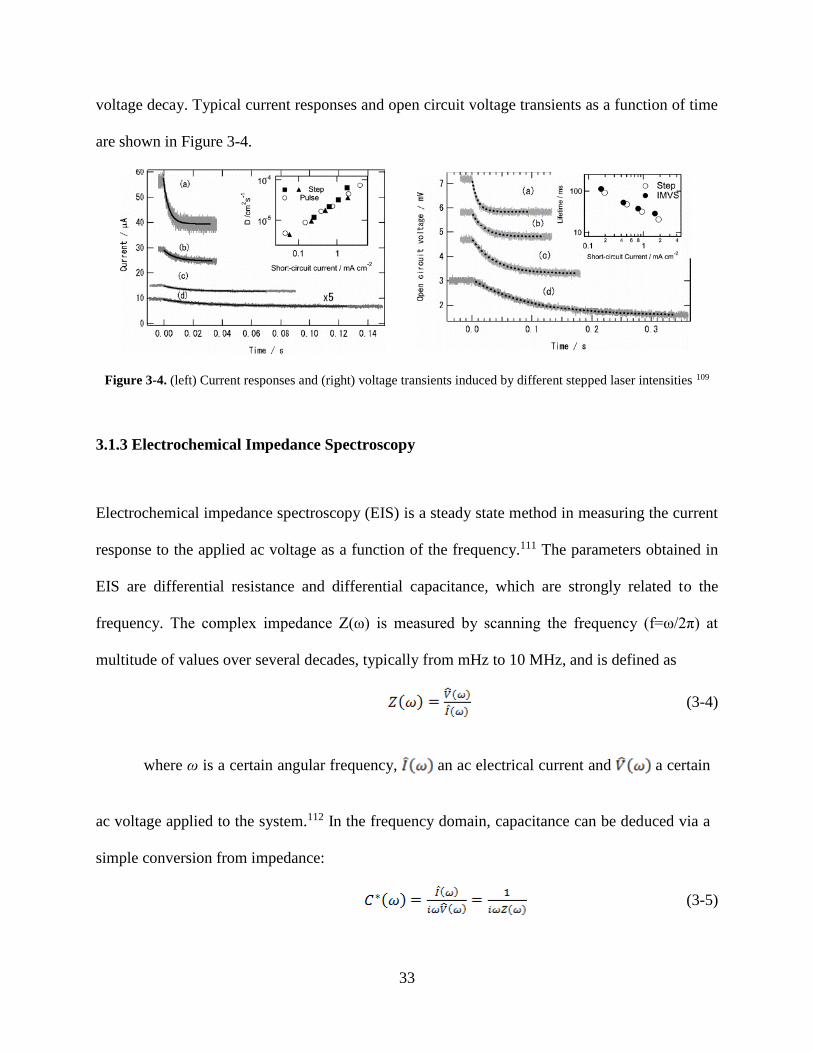
voltage decay. Typical current responses and open circuit voltage transients as a function of time
are shown in Figure 3-4.
Figure 3-4. (left) Current responses and (right) voltage transients induced by different stepped laser intensities 109
3.1.3 Electrochemical Impedance Spectroscopy
Electrochemical impedance spectroscopy (EIS) is a steady state method in measuring the current
response to the applied ac voltage as a function of the frequency.111 The parameters obtained in
EIS are differential resistance and differential capacitance, which are strongly related to the
frequency. The complex impedance Z(ω) is measured by scanning the frequency (f=ω/2π) at
multitude of values over several decades, typically from mHz to 10 MHz, and is defined as
(3-4)
where ω is a certain angular frequency, an ac electrical current and a certain
ac voltage applied to the system.112 In the frequency domain, capacitance can be deduced via a
simple conversion from impedance:
(3-5)
34
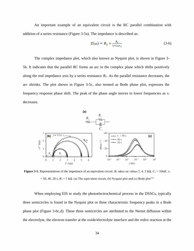
An important example of an equivalent circuit is the RC parallel combination with
addition of a series resistance (Figure 3-5a). The impedance is described as:
(3-6)
The complex impedance plot, which also known as Nyquist plot, is shown in Figure 3-
5b. It indicates that the parallel RC forms an arc in the complex plane which shifts positively
along the real impedance axis by a series resistance R2. As the parallel resistance decreases, the
arc shrinks. The plot shown in Figure 3-5c, also termed as Bode phase plot, expresses the
frequency response phase shift. The peak of the phase angle moves to lower frequencies as τ1
decreases.
Figure 3-5. Representations of the impedance of an equivalent circuit. R1 takes on values 5, 4, 2 kΩ, C1 = 10mF, τ1
= 50, 40, 20 s, R2 = 1 kΩ. (a) The equivalent circuit, (b) Nyquist plot and (c) Bode plot112
When employing EIS to study the photoelectrochemical process in the DSSCs, typically
three semicircles is found in the Nyquist plot or three characteristic frequency peaks in a Bode
phase plot (Figure 3-6c,d). These three semicircles are attributed to the Nernst diffusion within
the electrolyte, the electron transfer at the oxide/electrolyte interface and the redox reaction at the
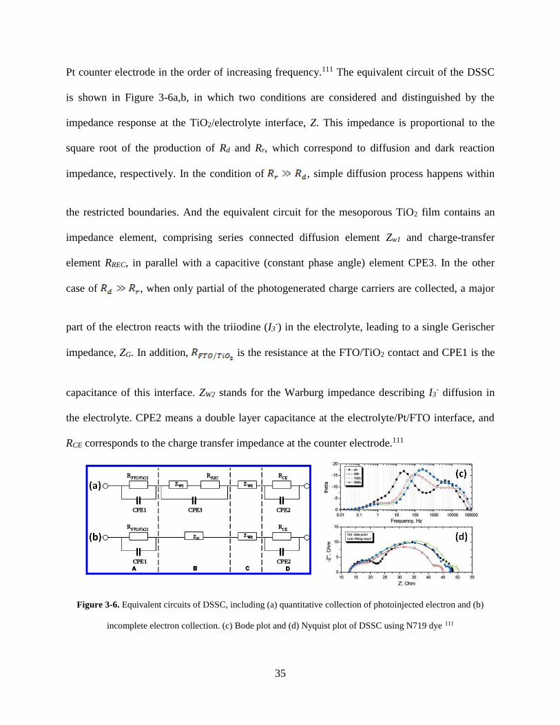
35
Pt counter electrode in the order of increasing frequency.111 The equivalent circuit of the DSSC
is shown in Figure 3-6a,b, in which two conditions are considered and distinguished by the
impedance response at the TiO2/electrolyte interface, Z. This impedance is proportional to the
square root of the production of Rd and Rr, which correspond to diffusion and dark reaction
impedance, respectively. In the condition of , simple diffusion process happens within
the restricted boundaries. And the equivalent circuit for the mesoporous TiO2 film contains an
impedance element, comprising series connected diffusion element Zw1 and charge-transfer
element RREC, in parallel with a capacitive (constant phase angle) element CPE3. In the other
case of , when only partial of the photogenerated charge carriers are collected, a major
part of the electron reacts with the triiodine (I3-) in the electrolyte, leading to a single Gerischer
impedance, ZG. In addition, is the resistance at the FTO/TiO2 contact and CPE1 is the
capacitance of this interface. ZW2 stands for the Warburg impedance describing I3- diffusion in
the electrolyte. CPE2 means a double layer capacitance at the electrolyte/Pt/FTO interface, and
RCE corresponds to the charge transfer impedance at the counter electrode.111
Figure 3-6. Equivalent circuits of DSSC, including (a) quantitative collection of photoinjected electron and (b)
incomplete electron collection. (c) Bode plot and (d) Nyquist plot of DSSC using N719 dye 111
36
3.2 PERFORMANCE ENHANCEMENT BY CORE-SHELL PARTICLES113
3.2.1 Sample Preparation and Characterization
Synthesis of SiO2 spheres and SiO2 core - Ag shell composites. The uniform SiO2 spheres
were prepared via Stöber method.114 Ammonium hydroxide (J. K. Baker, 28%) and tetra ethoxy
silane (TEOS, Sigma-Aldrich, 98%) were used as raw materials. The average diameter of silica
particles was controlled to be 400 nm.
The SiO2 core – Ag shell composites were synthesized by a seed mediated two-step
method (Figure 3-7). Ag nanoparticles were first formed on the surface of SiO2 particles, which
was followed by the subsequent deposition of the Ag thin layer. Ag nanoshell seeds were
synthesized by modifying the sonochemical reaction.81 Silica particles were added into deionized
water. Then, silver nitrate (Sigma-Aldrich, 99.8%) was dissolved in ammonium hydroxide
solution that was subsequently poured into the aqueous slurry of the SiO2 particles. After Ag
source and SiO2 particles were mixed, the slurry was sonicated for 3 hrs by using the high-
intensity ultrasound radiation. During the sonochemical reaction, temperature of the slurry was
maintained at 20 oC. Resulting particles were centrifuged and washed to remove residual
reagents. Purified particles were heated at a temperature of 100 oC under nitrogen gas flow for 3
hrs to crystallize silver nanoparticles on the surface of SiO2 particles. After thermal annealing,
the particles turned to be dark brown, indicating that Ag nanoparticles were nucleated on the
surface of the SiO2 particles.
37
Figure 3-7. Schematic procedure of preparation Ag@SiO2 core-shell particles by a seed mediated two-step method
These Ag nanoparticles were used as seeds to grow the thin silver layer in the next
reaction step. Dark brown powder (Ag seeds - SiO2 core), silver nitrate, and deionized water
were sequentially added into a 250 ml three-neck bottle and mixed well. At 85 oC, sodium
citrate was added into the aqueous mixture and was maintained at 85 oC for 1 - 3 hrs under
vigorous stirring. After the second reaction was finished, the SiO2 core – Ag shell composite
particles were obtained.
Preparation and characterization of TiO2 nanoparticle - composite mixture films.
Anatase TiO2 nanoparticles were prepared using a hydrothermal reaction.115 A mixture of
titanium (IV) isopropoxide (TTIP, Sigma-Aldrich, 97 %) and 2-propanol (J. K. Baker) was
slowly dripped into a mixture of acetic acid (Glacial, J. K. Baker) and deionized water at 0 oC.
Then, the solution was preheated at 80 oC for 8 hrs and was reacted at 220 oC for 6 hrs in a
microwave accelerated reaction system (MARS, CEM Co.). The phase of TiO2 nanoparticles is
anatase and the other phases (rutile and brookite) are not found in XRD patterns. A
38
microstructure of the hydrothermally grown nanoparticles is shown in a TEM micrograph of
Figure 3-8.
Figure 3-8. TEM image of TiO2 nanoparticles that are prepared by a hydrothermal route
Pure TiO2 nanoparticle films and TiO2 – composite mixture films were fabricated by a
recently reported chemical sintering method.116 A mixture of TiO2 slurry and core-shell
composite slurry were added with a small amount of ammonium hydroxide to increase the
viscosity of the mixed slurry. As a reference sample, a viscous paste of TiO2 nanoparticle -
uncoated SiO2 particle mixture was also prepared using a same method. The paste was spreaded
on a transparent conducting glass substrate (FTO) by the doctor-blade technique and annealed at
400 oC for 2 hrs under the flow of nitrogen gas.
The microstructure of the core-shell composite particles and the mixture films was
examined using scanning electron microscopy (SEM) (Model Philips XL 30) and transmission
electron microscopy (TEM) (Model JEM-200 CX, JEOL). The crystal structure of the core-shell
composite particles was determined using an X-ray diffractometer (XRD) (Model Philips
Analytical X-Ray). Absorption, transmission, and scattering of the core-shell particles and
39
mixture films were analyzed by UV/Vis spectrometer (Perkin Elmer, Lambda 35 UV/vis
Spectrometer) attached with an integrating sphere in the range from 300 nm to 900 nm.
Fabrication of DSSCs and characterization of their photovoltaic properties. The
TiO2 mixture films were sensitized in the solution of N719 dye [ruthenium (2,2’-bipyridy-4, 4’-
dicarboxylate)2(NCS)2, Solaronix SA, dissolved in ethanol] at room temperature for 24 hrs, and
then sandwiched with thermally platinized FTO counter electrode. Two substrates were
separated by 25 μm thick hot melt sealing tape (SX-1170-25, Solaronix SA) and the internal
space of the cell was filled with liquid electrolyte (Iodolyte AN-50, Solaronix SA) (Figure 3-9).
Figure 3-9. Schematic structure of the device which contains the core-shell particles embedded composite film
A part of sensitized thick films were immersed in NaOH solution to desorb the dyes. The
amounts of dyes desorbed from different photoelectrodes were examined by measuring UV/Vis
absorption spectra. The photovoltaic properties of the DSSCs were tested under AM 1.5 G
simulated sunlight (PV Measurements, Inc) with the aid of the electrochemical workstation (CHI
660 C). Incident photon to current efficiency curves (IPCE) of DSSCs was also measured by
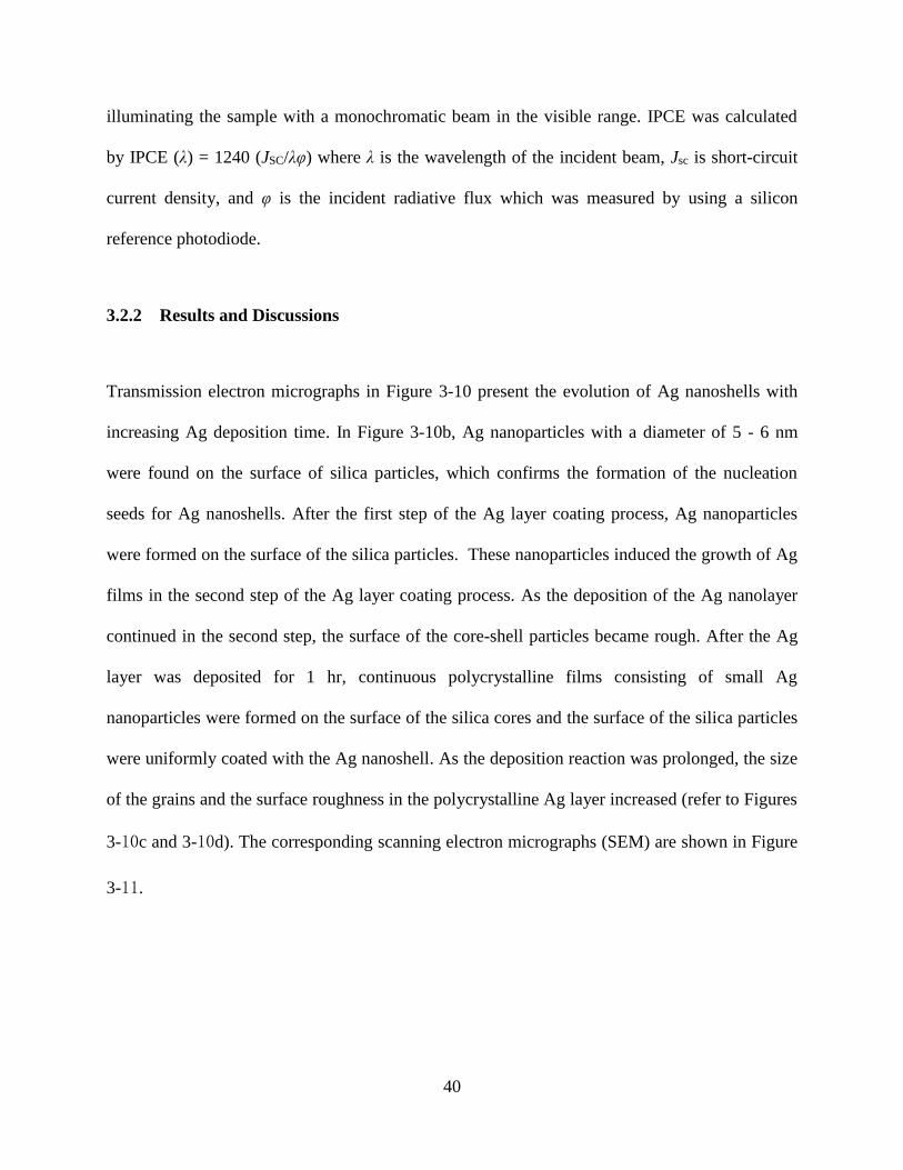
40
illuminating the sample with a monochromatic beam in the visible range. IPCE was calculated
by IPCE (λ) = 1240 (JSC/λφ) where λ is the wavelength of the incident beam, Jsc is short-circuit
current density, and φ is the incident radiative flux which was measured by using a silicon
reference photodiode.
3.2.2 Results and Discussions
Transmission electron micrographs in Figure 3-10 present the evolution of Ag nanoshells with
increasing Ag deposition time. In Figure 3-10b, Ag nanoparticles with a diameter of 5 - 6 nm
were found on the surface of silica particles, which confirms the formation of the nucleation
seeds for Ag nanoshells. After the first step of the Ag layer coating process, Ag nanoparticles
were formed on the surface of the silica particles. These nanoparticles induced the growth of Ag
films in the second step of the Ag layer coating process. As the deposition of the Ag nanolayer
continued in the second step, the surface of the core-shell particles became rough. After the Ag
layer was deposited for 1 hr, continuous polycrystalline films consisting of small Ag
nanoparticles were formed on the surface of the silica cores and the surface of the silica particles
were uniformly coated with the Ag nanoshell. As the deposition reaction was prolonged, the size
of the grains and the surface roughness in the polycrystalline Ag layer increased (refer to Figures
3-10c and 3-10d). The corresponding scanning electron micrographs (SEM) are shown in Figure
3-11.

41
Figure 3-10. TEM micrographs of (a) bare silica spheres, (b) silica particles coated with Ag seeds, (c) two-step
grown silica@Ag core-shell particles with the Ag layer being deposited for 1 hr, and (d) two-step grown silica@Ag
core-shell particles with the Ag layer being deposited for 3 hrs (black scale bar in insets = 200 nm)
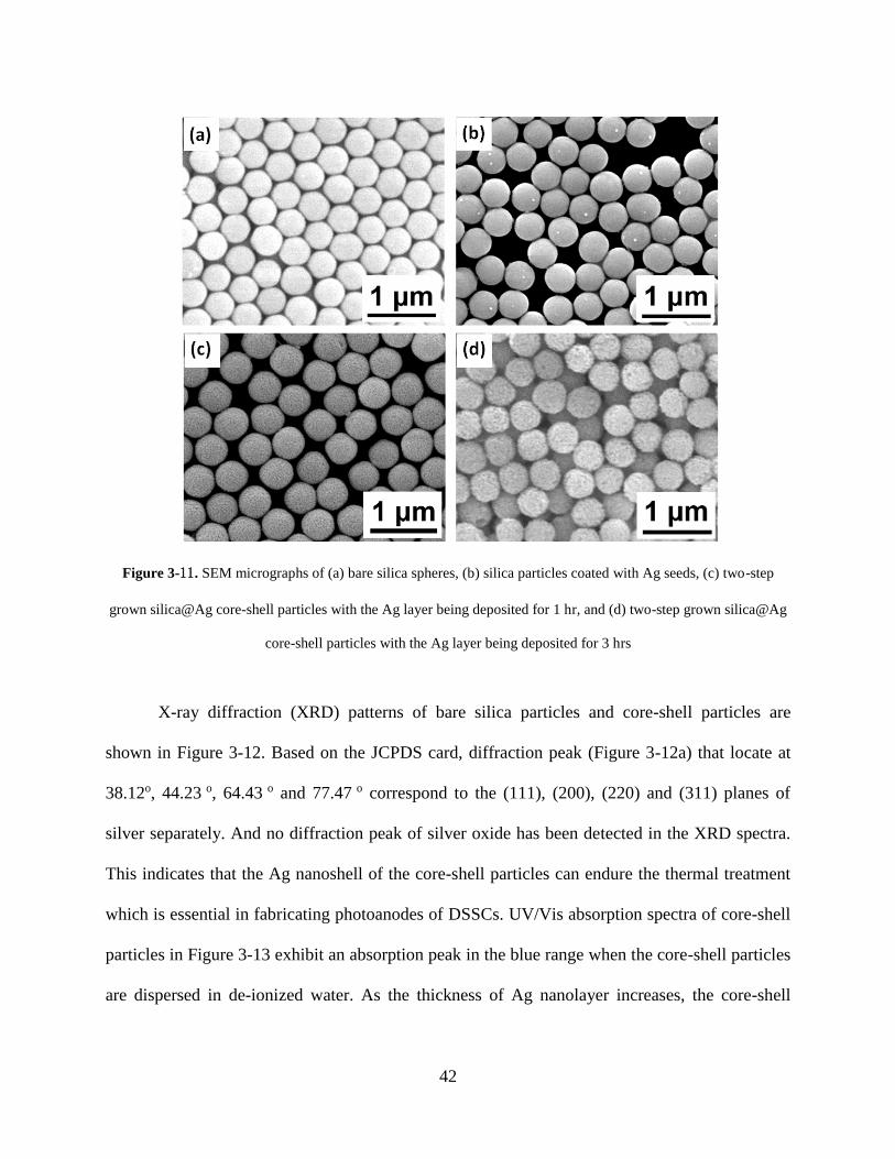
42
Figure 3-11. SEM micrographs of (a) bare silica spheres, (b) silica particles coated with Ag seeds, (c) two-step
grown silica@Ag core-shell particles with the Ag layer being deposited for 1 hr, and (d) two-step grown silica@Ag
core-shell particles with the Ag layer being deposited for 3 hrs
X-ray diffraction (XRD) patterns of bare silica particles and core-shell particles are
shown in Figure 3-12. Based on the JCPDS card, diffraction peak (Figure 3-12a) that locate at
38.12o, 44.23 o, 64.43 o and 77.47 o correspond to the (111), (200), (220) and (311) planes of
silver separately. And no diffraction peak of silver oxide has been detected in the XRD spectra.
This indicates that the Ag nanoshell of the core-shell particles can endure the thermal treatment
which is essential in fabricating photoanodes of DSSCs. UV/Vis absorption spectra of core-shell
particles in Figure 3-13 exhibit an absorption peak in the blue range when the core-shell particles
are dispersed in de-ionized water. As the thickness of Ag nanolayer increases, the core-shell
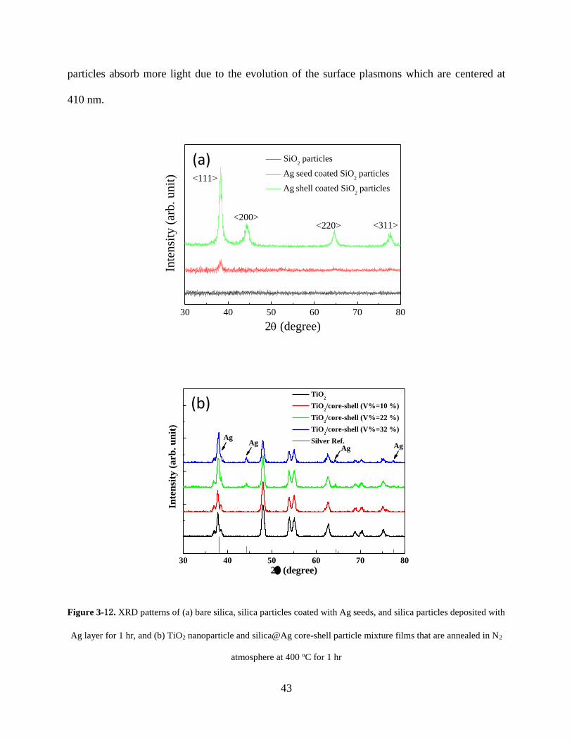
43
particles absorb more light due to the evolution of the surface plasmons which are centered at
410 nm.
30 40 50 60 70 80
<311><220><200>
Inte
nsi
ty (
arb
. u
nit
)
2 (degree)
SiO2 particles
Ag seed coated SiO2 particles
Ag shell coated SiO2 particles
<111>
(a)
30 40 50 60 70 80
AgAg
Ag
2 (degree)
TiO2
TiO2/core-shell (V%=10 %)
TiO2/core-shell (V%=22 %)
TiO2/core-shell (V%=32 %)
Silver Ref.
Inte
nsi
ty (
arb
. u
nit
)
Ag
(b)
Figure 3-12. XRD patterns of (a) bare silica, silica particles coated with Ag seeds, and silica particles deposited with
Ag layer for 1 hr, and (b) TiO2 nanoparticle and silica@Ag core-shell particle mixture films that are annealed in N2
atmosphere at 400 oC for 1 hr
44
300 400 500 600 700 800 900
4
3
2
1
0
Wavelength (nm)
Ab
sorb
ance
Figure 3-13. UV/Vis absorption curves of silica particles coated with Ag seeds and SiO2 core – Ag shell particles
with Ag layer being coated for 1 and 3 hrs
Structural and optical analyses of the core-shell particles show that 1 hr deposition
provides a uniform, smooth, and highly-crystalline Ag layer that can absorb enough light to
excite the surface plasmons. Therefore, 1 hr reaction was selected as the coating time of Ag
shells onto SiO2 cores in examining the effect of the surface plasmons on the light absorption and
photon-electron conversion of DSSCs. The 1 hr reacted core-shell particles were mixed with
TiO2 nanoparticles and chemically agglomerated to yield several m thick composite films.
Figure 3-14 shows SEM micrographs of the composite films in both plane-view and cross-
section. Large particles in the micrographs are core-shell particles that are uniformly dispersed
within the composite films. The distance between core-shell particles decreases as the volume
fraction of core-shell particles increases. For 22 vol% core-shell particles the mean distance
between the surfaces of core-shell particles was about 300 nm. To confirm the uniform
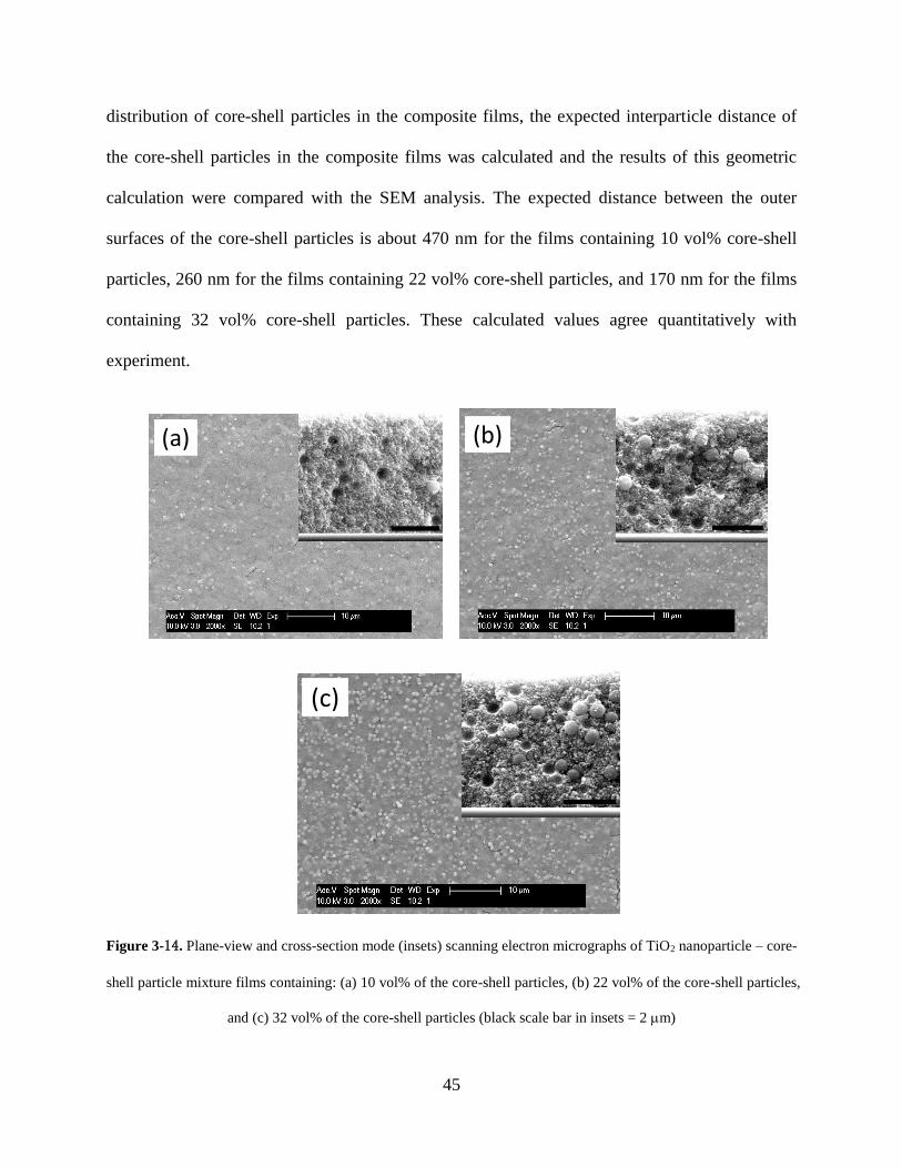
45
distribution of core-shell particles in the composite films, the expected interparticle distance of
the core-shell particles in the composite films was calculated and the results of this geometric
calculation were compared with the SEM analysis. The expected distance between the outer
surfaces of the core-shell particles is about 470 nm for the films containing 10 vol% core-shell
particles, 260 nm for the films containing 22 vol% core-shell particles, and 170 nm for the films
containing 32 vol% core-shell particles. These calculated values agree quantitatively with
experiment.
A(a) B(b)
C(c)
Figure 3-14. Plane-view and cross-section mode (insets) scanning electron micrographs of TiO2 nanoparticle – core-
shell particle mixture films containing: (a) 10 vol% of the core-shell particles, (b) 22 vol% of the core-shell particles,
and (c) 32 vol% of the core-shell particles (black scale bar in insets = 2 m)
46
UV/Vis absorption spectra of 5 m thick composite films are presented in Figure 3-15a.
For the precise measurement of thick films, UV/Vis spectroscopy analysis was performed in air
using an integrating sphere. Since there is a tradeoff between the plasmonic effect and the
decreased surface area in the core-shell particle added TiO2 film, the change in the optical
properties of the composite films with different core-shell loadings was systematically
investigated. A composite film of bare SiO2 particles and TiO2 nanoparticles was also prepared
as a control sample to qualitatively separate the surface plasmonic effect of the Ag shell from the
geometrical scattering effect of SiO2 cores. When the content of core-shell particles reaches 22
vol%, the mixed films show a dramatic increase in the absorption spectrum in visible range with
the appearance of a broad peak ranging from 450 nm to 700 nm. Compared with the absorption
spectra of core-shell particles dispersed in water, the absorption peak of the composite films
exhibits red-shift to 550 nm, which is due to the change in the refractive index of the medium
surrounding the core-shell particles. Since the porosity of the mixture films is larger than 50%,
the space near the core-shell particles is occupied by anatase TiO2 and air. Given that the
refractive index is ~2.49 in anatase TiO2, ~1.33 in water and ~1 in air, the refractive index of the
composite films increases and the absorption of the peak moves to longer wavelength. This
broad absorption peak is also observed in the transmittance spectra of core-shell particle added
TiO2 films in Figure 3-15b. In a bare SiO2 particle added composite film, the decrease in the
transmittance is less than that of the film containing the same amount of the core-shell particles
and a specific peak is not found. In Figure 3-15c, the reflectance of the core-shell particle added
mixture films is increased in the red range, which is not found in TiO2 films and TiO2-SiO2
composite films. The increase in the reflectance of the core-shell particle added films is traced to
the large scattering cross-section and multiple scattering of the core-shell particles.
47
In contrast to the core-shell particles, a bare SiO2 particle added film exhibits a
reflectance spectrum whose shape is very similar to the pure TiO2 film. A difference in the level
of absolute reflectance between these two films is attributed to the scattering of large SiO2
particles in the visible range. This clearly indicates that the core-shell particles change the
passage of the photons in the composite films and simple geometrical scattering of SiO2 cores is
not mainly responsible for the optical properties of the composite films. UV/Vis spectra shown
in Figure 3-15 suggest that localized surface plasmons in the core-shell type composites increase
the scattering and absorption of incoming light. A comparison of the experimental results with
the theoretical calculations (Fig. 2-1) shows that the reflectance of TiO2/core-shell mixture films
is well explained when the Ag nanoshell is assumed to be a perfect film. Contradictory
conclusions from the absorption and scattering efficiencies indicate that the Ag shells used in our
study have characteristics of both particles and films and those two different mechanisms
contribute to enhancing the optical field near the core-shell particles.
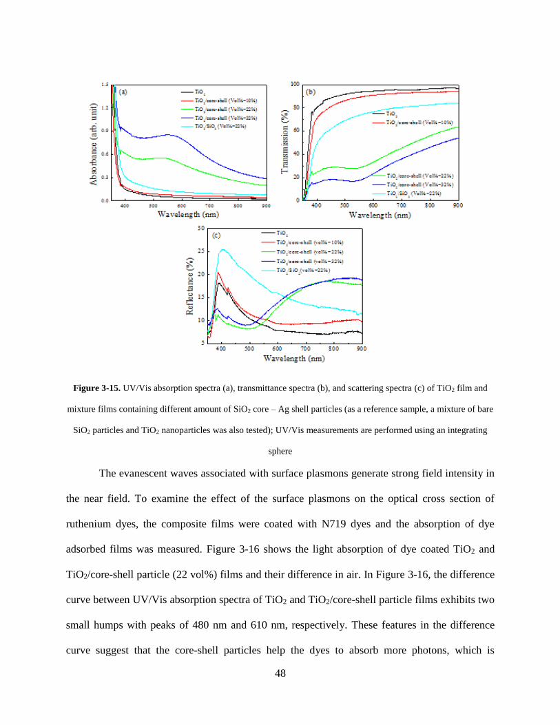
48
Figure 3-15. UV/Vis absorption spectra (a), transmittance spectra (b), and scattering spectra (c) of TiO2 film and
mixture films containing different amount of SiO2 core – Ag shell particles (as a reference sample, a mixture of bare
SiO2 particles and TiO2 nanoparticles was also tested); UV/Vis measurements are performed using an integrating
sphere
The evanescent waves associated with surface plasmons generate strong field intensity in
the near field. To examine the effect of the surface plasmons on the optical cross section of
ruthenium dyes, the composite films were coated with N719 dyes and the absorption of dye
adsorbed films was measured. Figure 3-16 shows the light absorption of dye coated TiO2 and
TiO2/core-shell particle (22 vol%) films and their difference in air. In Figure 3-16, the difference
curve between UV/Vis absorption spectra of TiO2 and TiO2/core-shell particle films exhibits two
small humps with peaks of 480 nm and 610 nm, respectively. These features in the difference
curve suggest that the core-shell particles help the dyes to absorb more photons, which is
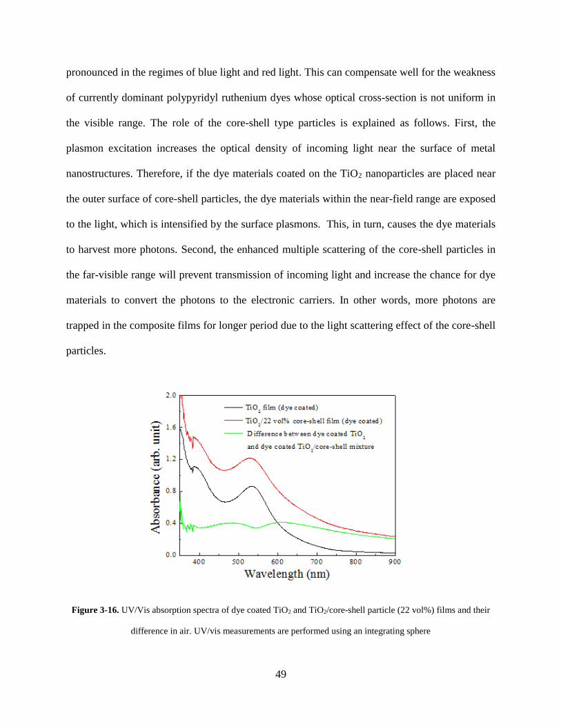
49
pronounced in the regimes of blue light and red light. This can compensate well for the weakness
of currently dominant polypyridyl ruthenium dyes whose optical cross-section is not uniform in
the visible range. The role of the core-shell type particles is explained as follows. First, the
plasmon excitation increases the optical density of incoming light near the surface of metal
nanostructures. Therefore, if the dye materials coated on the TiO2 nanoparticles are placed near
the outer surface of core-shell particles, the dye materials within the near-field range are exposed
to the light, which is intensified by the surface plasmons. This, in turn, causes the dye materials
to harvest more photons. Second, the enhanced multiple scattering of the core-shell particles in
the far-visible range will prevent transmission of incoming light and increase the chance for dye
materials to convert the photons to the electronic carriers. In other words, more photons are
trapped in the composite films for longer period due to the light scattering effect of the core-shell
particles.
Figure 3-16. UV/Vis absorption spectra of dye coated TiO2 and TiO2/core-shell particle (22 vol%) films and their
difference in air. UV/vis measurements are performed using an integrating sphere
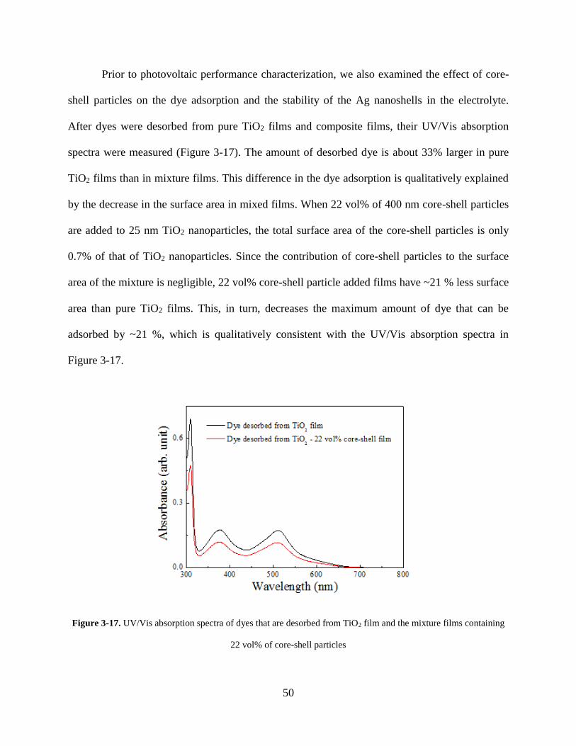
50
Prior to photovoltaic performance characterization, we also examined the effect of core-
shell particles on the dye adsorption and the stability of the Ag nanoshells in the electrolyte.
After dyes were desorbed from pure TiO2 films and composite films, their UV/Vis absorption
spectra were measured (Figure 3-17). The amount of desorbed dye is about 33% larger in pure
TiO2 films than in mixture films. This difference in the dye adsorption is qualitatively explained
by the decrease in the surface area in mixed films. When 22 vol% of 400 nm core-shell particles
are added to 25 nm TiO2 nanoparticles, the total surface area of the core-shell particles is only
0.7% of that of TiO2 nanoparticles. Since the contribution of core-shell particles to the surface
area of the mixture is negligible, 22 vol% core-shell particle added films have ~21 % less surface
area than pure TiO2 films. This, in turn, decreases the maximum amount of dye that can be
adsorbed by ~21 %, which is qualitatively consistent with the UV/Vis absorption spectra in
Figure 3-17.
Figure 3-17. UV/Vis absorption spectra of dyes that are desorbed from TiO2 film and the mixture films containing
22 vol% of core-shell particles
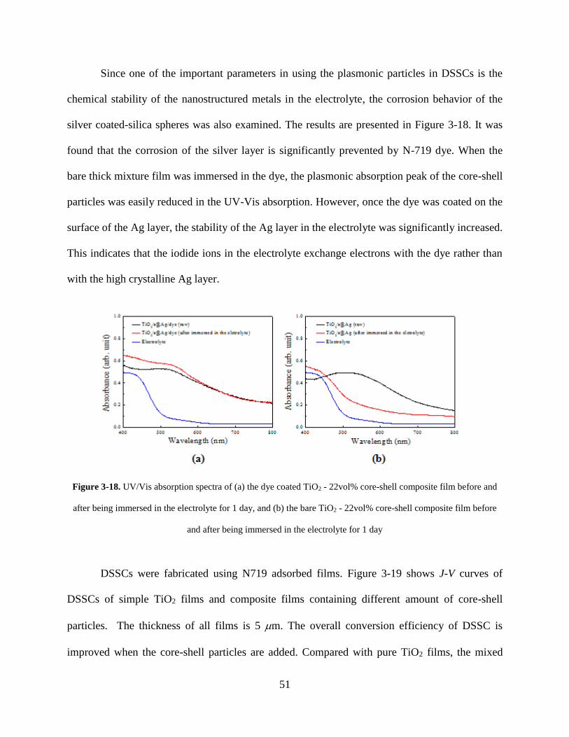
51
Since one of the important parameters in using the plasmonic particles in DSSCs is the
chemical stability of the nanostructured metals in the electrolyte, the corrosion behavior of the
silver coated-silica spheres was also examined. The results are presented in Figure 3-18. It was
found that the corrosion of the silver layer is significantly prevented by N-719 dye. When the
bare thick mixture film was immersed in the dye, the plasmonic absorption peak of the core-shell
particles was easily reduced in the UV-Vis absorption. However, once the dye was coated on the
surface of the Ag layer, the stability of the Ag layer in the electrolyte was significantly increased.
This indicates that the iodide ions in the electrolyte exchange electrons with the dye rather than
with the high crystalline Ag layer.
Figure 3-18. UV/Vis absorption spectra of (a) the dye coated TiO2 - 22vol% core-shell composite film before and
after being immersed in the electrolyte for 1 day, and (b) the bare TiO2 - 22vol% core-shell composite film before
and after being immersed in the electrolyte for 1 day
DSSCs were fabricated using N719 adsorbed films. Figure 3-19 shows J-V curves of
DSSCs of simple TiO2 films and composite films containing different amount of core-shell
particles. The thickness of all films is 5 m. The overall conversion efficiency of DSSC is
improved when the core-shell particles are added. Compared with pure TiO2 films, the mixed
52
films containing 22 vol% core-shell particles increase the efficiency from 2.7 % to 4.0 %. Given
that 22% decrease in the surface area of the composite film reduces the amount of the adsorbed
dye, this increase in the efficiency indicates that the well-arranged core-shell particles can
enhance the energy conversion capability of the dye molecule in the near-field by up to 80%.
The higher energy conversion efficiency of core-shell particle embedded DSSC is due to the
increase in both short circuit current (Jsc) and open circuit voltage (Voc). Jsc of DSSCs containing
22 vol% core-shell particles is 7.8 mA cm-2, which is higher than the Jsc of pure TiO2 film based
DSSCs (5.9 mA cm-2). The addition of core-shell particles also slightly increases Voc from 0.63
V to 0.76 V. Given that the amount of dye adsorbed on TiO2 films is 33% larger than the mixed
films and the same TiO2 nanoparticles are used in both films, this difference cannot be attributed
to dye content or transport kinetics of electrons in the films. The energy conversion efficiency of
DSSCs is moderately improved to 3.0 % and 3.4 % for core-shell particle fractions of 10 vol%
and 32 vol%. The effect of the core-shell particles on Jsc is attributed to the combined effect of
the increased light intensity and the decreased surface area (see next section for explanation). In
addition, it is noted that DSSCs using 32 vol% core-shell particles possess higher open circuit
voltage and slightly lower short circuit current than DSSCs using only TiO2. This increase in Voc
may be attributed to the reduced recombination of photogenerated carriers, with the large core-
shell particles impeding back-reaction with tri-iodide ions in the electrolyte.

53
Figure 3-19. J-V curves of DSSCs using TiO2 film or mixture films containing different amount of core shell
particles, as photoanodes (as a reference sample, the TiO2 - SiO2 mixture film was also tested)
Figure 3-20 shows the lifetime of electrons in DSSCs using pure TiO2 and TiO2 –
22vol% core-shell particle composite films to examine the correlation between the core-shell
particles and the retarded back electron transfer. The transient of Voc was measured as a function
of time by using a 633nm photodiode laser as the light source. Then, the carrier lifetime in
different DSSCs were calculated from the decay curves of Voc (inset of Figure 3-20).107 The
addition of the core-shell particles significantly increases the carrier lifetime, indicating the
suppressed recombination of the photogenerated carriers and the backward transfer of electrons
from the TiO2 films to the electrolyte in the presence of the core-shell particles. Additional
information on the backward electron transfer and carrier life time that is consistent with the
transient of Voc, are presented in Figure 3-21.
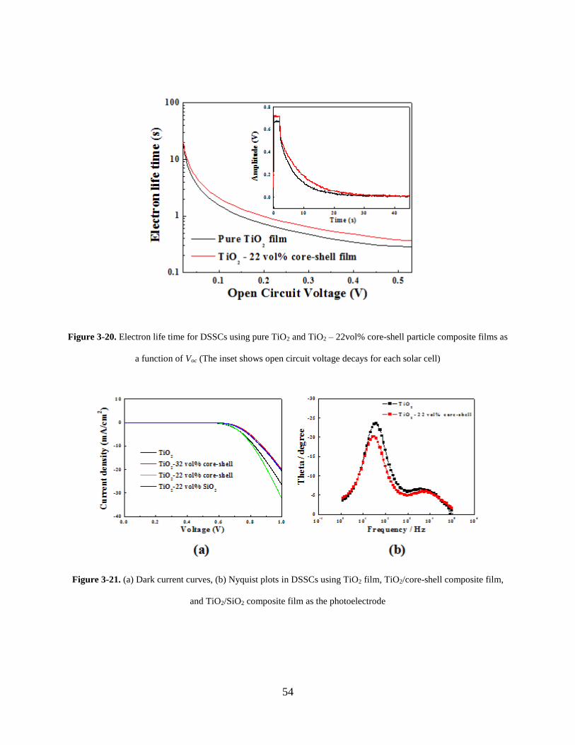
54
Figure 3-20. Electron life time for DSSCs using pure TiO2 and TiO2 – 22vol% core-shell particle composite films as
a function of Voc (The inset shows open circuit voltage decays for each solar cell)
Figure 3-21. (a) Dark current curves, (b) Nyquist plots in DSSCs using TiO2 film, TiO2/core-shell composite film,
and TiO2/SiO2 composite film as the photoelectrode
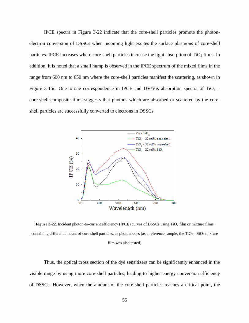
55
IPCE spectra in Figure 3-22 indicate that the core-shell particles promote the photon-
electron conversion of DSSCs when incoming light excites the surface plasmons of core-shell
particles. IPCE increases where core-shell particles increase the light absorption of TiO2 films. In
addition, it is noted that a small hump is observed in the IPCE spectrum of the mixed films in the
range from 600 nm to 650 nm where the core-shell particles manifest the scattering, as shown in
Figure 3-15c. One-to-one correspondence in IPCE and UV/Vis absorption spectra of TiO2 –
core-shell composite films suggests that photons which are absorbed or scattered by the core-
shell particles are successfully converted to electrons in DSSCs.
Figure 3-22. Incident photon-to-current efficiency (IPCE) curves of DSSCs using TiO2 film or mixture films
containing different amount of core shell particles, as photoanodes (as a reference sample, the TiO2 - SiO2 mixture
film was also tested)
Thus, the optical cross section of the dye sensitizers can be significantly enhanced in the
visible range by using more core-shell particles, leading to higher energy conversion efficiency
of DSSCs. However, when the amount of the core-shell particles reaches a critical point, the

56
trade-off between the smaller surface area and the increase in the optical cross section of the dye
restricts the effect of the surface plasmons on the photon-electron conversion, as demonstrated in
DSSCs containing 32 vol% core-shell particles.

57
4.0 PLASMONIC TUNING EFFECT IN DSSC
4.1 BACKGROUND
Metallic nanostructures, a new class of photonic components, have rapidly developed during the
past decade. This is due to their ability to control and manipulate light at the nanoscale level,
which is related on localized surface plasmons (SPs).1, 2 SPs are a result of optically induced
oscillations of the free electrons,64 which can be coupled to the optical wave as propagating
surface waves or localized excitations. SPs are strongly depended on the topology and geometry
of the metallic nanostructures.117-119 In particular, plasmonic core-shell particles, which consist of
a spherical dielectric core coated with a concentric layer of metallic nanoshell, are versatile
subwavelength optical components, the surface plasmon resonance of which can be tuned by
simply varying the thickness of the metallic nanoshell and the diameter of the inner core.30, 31
This unique adjustable nature of the plasmonic core-shell particles facilitates their applications in
surface-enhanced Raman spectroscopy,120, 121 high-resolusion bioimaging,122, 123 thermal
therapy,124 and drug delivery.125
Recently, SPs have been extensively studied to determine their ability to enhance the
light absorption of solar cells.65 Specifically, analysis has focused on the extent to which the
excitation of localized SPs traps incoming photons and is coupled to light absorption capability
of surrounding semiconductor. Furthermore, studies show that the effective optical path length

58
can be dramatically increased by multiple and high-angle light scattering from the metallic
nanostructures in the cell.
TiO2 nanoparticle-based dye sensitized solar cells (DSSCs) have attracted a vast amount
of scientific and technological interest for their potential cost effectiveness.40 However, DSSCs
suffer from a relatively small optical cross section of dye molecules and a mismatch between the
dye absorption spectrum and the solar spectrum.41-43 One possible way to improve the light
absorption of DSSCs is to increase the thickness of the photoelectrode. However, as the
photoelectrode gets thicker, carrier diffusion length becomes comparable to the thickness of the
photoelectrode and carrier collection efficiency starts to decrease.65 Hence, when the
photoelectrode is thicker than 20 μm, the effect of the photoelectrode thickness on the efficiency
of DSSCs is saturated.126 In addition, the increase in the thickness of TiO2 film deteriorates open
circuit voltage (Voc) and fill factor, because of the increased back electron transfer between I3-
ions and conduction band electrons in TiO2 film.127
SPs have been found to be an effective way to improve the energy conversion efficiency
in DSSCs without increasing the thickness of the photoelectrode, since its generated plasmonic
near-field can increase the absorption and/or scattering of incoming light. Both bare128 and
surface coated metallic nanoparticles85, 86, 104 were successfully explored in DSSCs for light
harvesting. However, their plasmonic frequency is pre-determined by the type of metals and less
influenced by the size of the nanoparticles. Therefore, the metal nanoparticles may have
difficulty in matching the frequency of the surface plasmons with the dye absorption spectrum,
which depend on the unique molecular structure of dyes.129-132 To address this problem, several
groups have changed the shape of the nanostructure metals and shifted the surface plasmon
frequency within the absorption spectrum of DSSCs. Chang et al. investigated the role of Au
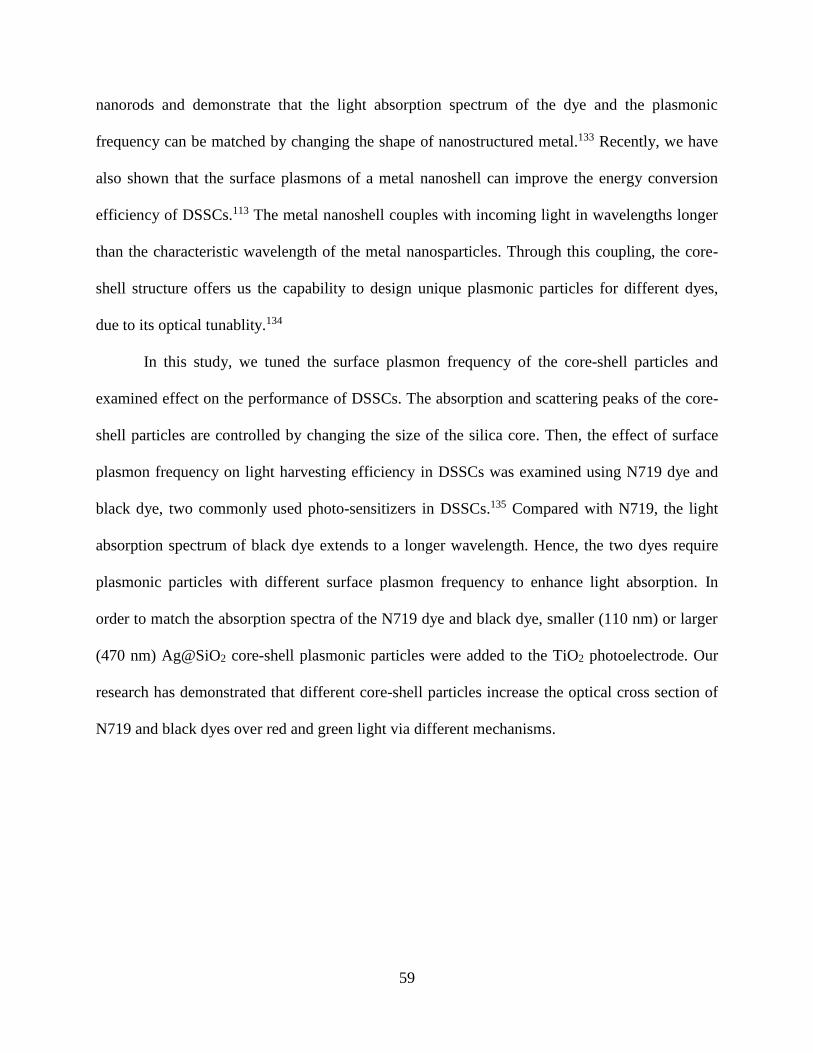
59
nanorods and demonstrate that the light absorption spectrum of the dye and the plasmonic
frequency can be matched by changing the shape of nanostructured metal.133 Recently, we have
also shown that the surface plasmons of a metal nanoshell can improve the energy conversion
efficiency of DSSCs.113 The metal nanoshell couples with incoming light in wavelengths longer
than the characteristic wavelength of the metal nanosparticles. Through this coupling, the core-
shell structure offers us the capability to design unique plasmonic particles for different dyes,
due to its optical tunablity.134
In this study, we tuned the surface plasmon frequency of the core-shell particles and
examined effect on the performance of DSSCs. The absorption and scattering peaks of the core-
shell particles are controlled by changing the size of the silica core. Then, the effect of surface
plasmon frequency on light harvesting efficiency in DSSCs was examined using N719 dye and
black dye, two commonly used photo-sensitizers in DSSCs.135 Compared with N719, the light
absorption spectrum of black dye extends to a longer wavelength. Hence, the two dyes require
plasmonic particles with different surface plasmon frequency to enhance light absorption. In
order to match the absorption spectra of the N719 dye and black dye, smaller (110 nm) or larger
(470 nm) Ag@SiO2 core-shell plasmonic particles were added to the TiO2 photoelectrode. Our
research has demonstrated that different core-shell particles increase the optical cross section of
N719 and black dyes over red and green light via different mechanisms.
60
4.2 TUNING EFFECT OF SILVER NANOSHELL – SILICA CORE PARTICLES IN
DSSC136
4.2.1 Sample Preparation and Characterization
SiO2 spheres with uniform diameters were synthesized by Stöber method. By varying the volume
ratio of these chemicals, the diameters of the silica spheres could be controlled as 90 nm and 450
nm separately. Ag@SiO2 core – shell particles were fabricated following a two-step method.113
Typically, to prepare core-shell particles with an average diameter of 110 nm, 15 ml of freshly
prepared [Ag(NH3)2]+ ion solution was added into 100 ml aqueous solution containing 225 mg
silica nanospheres whose average diameter was 90 nm. The mixture was then sonicated for 3 hrs
at 20 oC by using the high-intensity ultrasound radiation. Resulting particles were centrifuged
and washed to remove residual reagents. Purified particles were heated at 100 oC under nitrogen
gas flow for 3 hrs to crystallize silver nanoparticles on the surface of SiO2 particles. After
thermal annealing, the fine powder turned to be dark brown, indicating that Ag nanoparticles
were nucleated on the surface of the SiO2 particles. These attached Ag nanoparticles were used
as seeds to grow the thin silver layer on the silica cores in the future. During the second step, 27
mg dark brown powder (Ag seeds - SiO2 core) and 100 ml aqueous solution containing 2.4 mM
silver nitrate were sequentially added into a 250 ml three-neck bottle and mixed well. At 85 oC,
55 mg sodium citrate was added into the aqueous mixture and was maintained at 85 oC for 1 hr
under vigorous stirring. After purification, Ag@SiO2 core – shell particles with an average
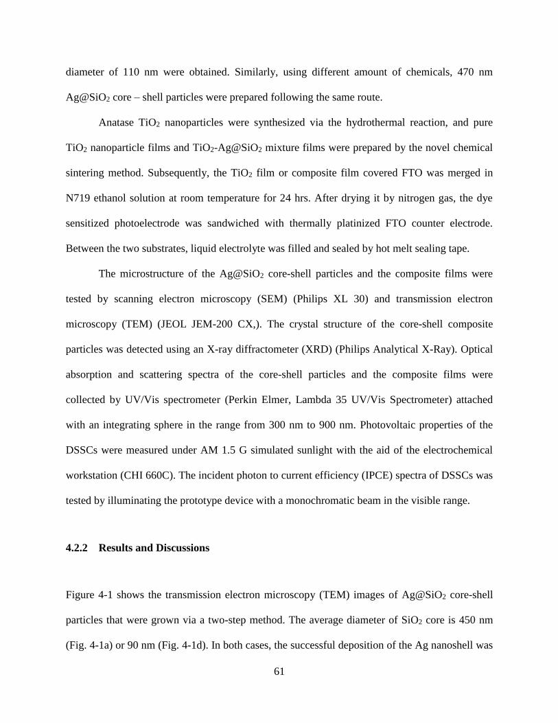
61
diameter of 110 nm were obtained. Similarly, using different amount of chemicals, 470 nm
Ag@SiO2 core – shell particles were prepared following the same route.
Anatase TiO2 nanoparticles were synthesized via the hydrothermal reaction, and pure
TiO2 nanoparticle films and TiO2-Ag@SiO2 mixture films were prepared by the novel chemical
sintering method. Subsequently, the TiO2 film or composite film covered FTO was merged in
N719 ethanol solution at room temperature for 24 hrs. After drying it by nitrogen gas, the dye
sensitized photoelectrode was sandwiched with thermally platinized FTO counter electrode.
Between the two substrates, liquid electrolyte was filled and sealed by hot melt sealing tape.
The microstructure of the Ag@SiO2 core-shell particles and the composite films were
tested by scanning electron microscopy (SEM) (Philips XL 30) and transmission electron
microscopy (TEM) (JEOL JEM-200 CX,). The crystal structure of the core-shell composite
particles was detected using an X-ray diffractometer (XRD) (Philips Analytical X-Ray). Optical
absorption and scattering spectra of the core-shell particles and the composite films were
collected by UV/Vis spectrometer (Perkin Elmer, Lambda 35 UV/Vis Spectrometer) attached
with an integrating sphere in the range from 300 nm to 900 nm. Photovoltaic properties of the
DSSCs were measured under AM 1.5 G simulated sunlight with the aid of the electrochemical
workstation (CHI 660C). The incident photon to current efficiency (IPCE) spectra of DSSCs was
tested by illuminating the prototype device with a monochromatic beam in the visible range.
4.2.2 Results and Discussions
Figure 4-1 shows the transmission electron microscopy (TEM) images of Ag@SiO2 core-shell
particles that were grown via a two-step method. The average diameter of SiO2 core is 450 nm
(Fig. 4-1a) or 90 nm (Fig. 4-1d). In both cases, the successful deposition of the Ag nanoshell was
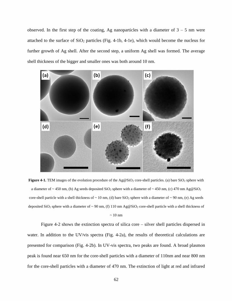
62
observed. In the first step of the coating, Ag nanoparticles with a diameter of 3 – 5 nm were
attached to the surface of SiO2 particles (Fig. 4-1b, 4-1e), which would become the nucleus for
further growth of Ag shell. After the second step, a uniform Ag shell was formed. The average
shell thickness of the bigger and smaller ones was both around 10 nm.
Figure 4-1. TEM images of the evolution procedure of the Ag@SiO2 core-shell particles. (a) bare SiO2 sphere with
a diameter of ~ 450 nm, (b) Ag seeds deposited SiO2 sphere with a diameter of ~ 450 nm, (c) 470 nm Ag@SiO2
core-shell particle with a shell thickness of ~ 10 nm, (d) bare SiO2 sphere with a diameter of ~ 90 nm, (e) Ag seeds
deposited SiO2 sphere with a diameter of ~ 90 nm, (f) 110 nm Ag@SiO2 core-shell particle with a shell thickness of
~ 10 nm
Figure 4-2 shows the extinction spectra of silica core – silver shell particles dispersed in
water. In addition to the UV/vis spectra (Fig. 4-2a), the results of theoretical calculations are
presented for comparison (Fig. 4-2b). In UV-vis spectra, two peaks are found. A broad plasmon
peak is found near 650 nm for the core-shell particles with a diameter of 110nm and near 800 nm
for the core-shell particles with a diameter of 470 nm. The extinction of light at red and infrared
63
regime is the result of absorption and scattering by Ag nanoshells. The correlation with size
clearly indicates that the wavelength of the coupled plasmon mode in core-shell particles can be
controlled by simply changing the size of the core. An increase in the extinction in the longer
wavelength is due to the size of the core-shell particles, and an appearance of the multiple peals
is attributed to a hybridization of charge oscillations at the outer and inner surfaces of the shell.31
In addition, both samples have a peak at 410 nm that corresponds to the plasmon resonance
frequency of silver nanoparticles. The shorter wavelength peak implies that Ag nanoshells also
interact with incoming light as nanoparticles that are physically attached to the outer surface of
the shell. The extinction coefficieny of the metal nanoshells or metal nanoparticles was
calculated via a generalized Mie scattering approach. Fig. 4-2b shows that the increase in the
core size shifts the peak of the extinction spectrum to a longer wavelength. Similarities in the
general trend between the experimental and theoretical results confirm our analysis of the
experimentally measured extinction spectra of the core-shell particles.94, 96 It is noted that the
width of the experimentally observed plasmon peaks is broader than the width of the calculated
plasmon peaks. Several factors contribute to this broadening effect of the plasmon peaks of the
silver nanoshell. One is the size distribution of the silica core diameter and the silver shell
thickness and the other is surface roughness of the silver nanoshells.31 In addition, if the mean
free path of the electrons is larger than the dimension of the nanoparticle, an extra broadening of
the surface plasmon peaks occurs.17
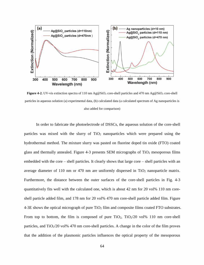
64
Figure 4-2. UV-vis extinction spectra of 110 nm Ag@SiO2 core-shell particles and 470 nm Ag@SiO2 core-shell
particles in aqueous solution (a) experimental data, (b) calculated data (a calculated spectrum of Ag nanoparticles is
also added for comparison)
In order to fabricate the photoelectrode of DSSCs, the aqueous solution of the core-shell
particles was mixed with the slurry of TiO2 nanoparticles which were prepared using the
hydrothermal method. The mixture slurry was pasted on fluorine doped tin oxide (FTO) coated
glass and thermally annealed. Figure 4-3 presents SEM micrographs of TiO2 mesoporous films
embedded with the core – shell particles. It clearly shows that large core – shell particles with an
average diameter of 110 nm or 470 nm are uniformly dispersed in TiO2 nanoparticle matrix.
Furthermore, the distance between the outer surfaces of the core-shell particles in Fig. 4-3
quantitatively fits well with the calculated one, which is about 42 nm for 20 vol% 110 nm core-
shell particle added film, and 178 nm for 20 vol% 470 nm core-shell particle added film. Figure
4-3E shows the optical micrograph of pure TiO2 film and composite films coated FTO substrates.
From top to bottom, the film is composed of pure TiO2, TiO2/20 vol% 110 nm core-shell
particles, and TiO2/20 vol% 470 nm core-shell particles. A change in the color of the film proves
that the addition of the plasmonic particles influences the optical property of the mesoporous

65
films. The silver phase in the mixture film is well crystallized during a thermal annealing
procedure. In addition, a stronger intensity of silver XRD peaks for the 110 nm core-shell
particle added film, is due to the higher surface area of smaller core-shell particles (Fig. 4-4).
Figure 4-3. SEM plan-view image of 20 vol% (a) 110 nm and (b) 470 nm Ag@SiO2 core-shell particles embedded
TiO2 mesoporous film. SEM cross-section image of 20 vol% (c) 110 nm and (d) 470 nm Ag@SiO2 core-shell
particles embedded TiO2 mesoporous film. (e) an optical micrograph of photoanode coated FTO substrate. From top
to bottom, the photoanode is pure TiO2 film, 20 vol% 110 nm Ag@SiO2 embedded TiO2 mesoporous film, and 20
vol% 470 nm Ag@SiO2 embedded TiO2 mesoporous film, separately. The area of the film is 5 5 mm2
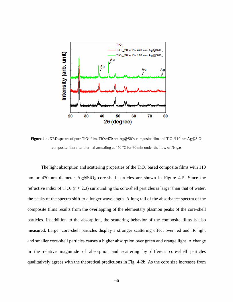
66
Figure 4-4. XRD spectra of pure TiO2 film, TiO2/470 nm Ag@SiO2 composite film and TiO2/110 nm Ag@SiO2
composite film after thermal annealing at 450 oC for 30 min under the flow of N2 gas
The light absorption and scattering properties of the TiO2 based composite films with 110
nm or 470 nm diameter Ag@SiO2 core-shell particles are shown in Figure 4-5. Since the
refractive index of TiO2 (n ≈ 2.3) surrounding the core-shell particles is larger than that of water,
the peaks of the spectra shift to a longer wavelength. A long tail of the absorbance spectra of the
composite films results from the overlapping of the elementary plasmon peaks of the core-shell
particles. In addition to the absorption, the scattering behavior of the composite films is also
measured. Larger core-shell particles display a stronger scattering effect over red and IR light
and smaller core-shell particles causes a higher absorption over green and orange light. A change
in the relative magnitude of absorption and scattering by different core-shell particles
qualitatively agrees with the theoretical predictions in Fig. 4-2b. As the core size increases from
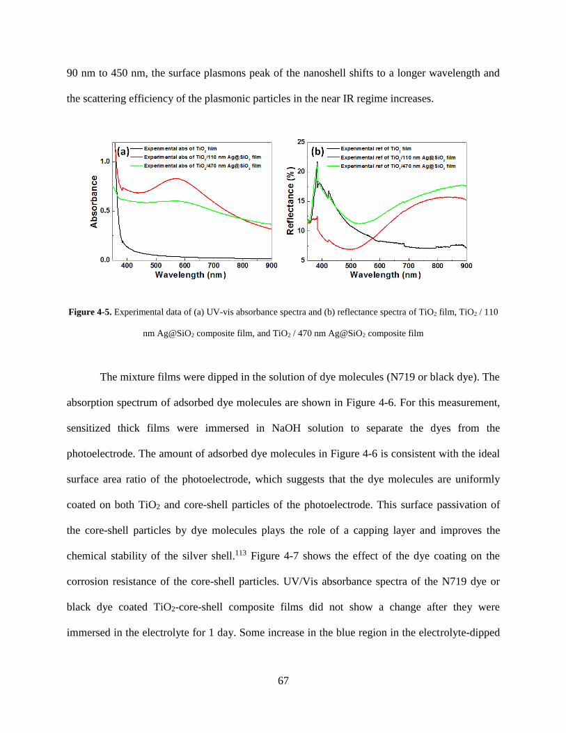
67
90 nm to 450 nm, the surface plasmons peak of the nanoshell shifts to a longer wavelength and
the scattering efficiency of the plasmonic particles in the near IR regime increases.
Figure 4-5. Experimental data of (a) UV-vis absorbance spectra and (b) reflectance spectra of TiO2 film, TiO2 / 110
nm Ag@SiO2 composite film, and TiO2 / 470 nm Ag@SiO2 composite film
The mixture films were dipped in the solution of dye molecules (N719 or black dye). The
absorption spectrum of adsorbed dye molecules are shown in Figure 4-6. For this measurement,
sensitized thick films were immersed in NaOH solution to separate the dyes from the
photoelectrode. The amount of adsorbed dye molecules in Figure 4-6 is consistent with the ideal
surface area ratio of the photoelectrode, which suggests that the dye molecules are uniformly
coated on both TiO2 and core-shell particles of the photoelectrode. This surface passivation of
the core-shell particles by dye molecules plays the role of a capping layer and improves the
chemical stability of the silver shell.113 Figure 4-7 shows the effect of the dye coating on the
corrosion resistance of the core-shell particles. UV/Vis absorbance spectra of the N719 dye or
black dye coated TiO2-core-shell composite films did not show a change after they were
immersed in the electrolyte for 1 day. Some increase in the blue region in the electrolyte-dipped
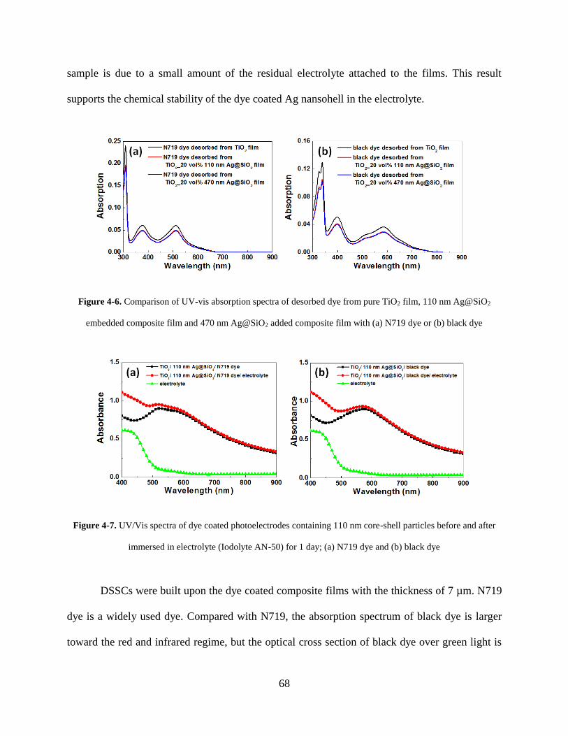
68
sample is due to a small amount of the residual electrolyte attached to the films. This result
supports the chemical stability of the dye coated Ag nansohell in the electrolyte.
Figure 4-6. Comparison of UV-vis absorption spectra of desorbed dye from pure TiO2 film, 110 nm Ag@SiO2
embedded composite film and 470 nm Ag@SiO2 added composite film with (a) N719 dye or (b) black dye
Figure 4-7. UV/Vis spectra of dye coated photoelectrodes containing 110 nm core-shell particles before and after
immersed in electrolyte (Iodolyte AN-50) for 1 day; (a) N719 dye and (b) black dye
DSSCs were built upon the dye coated composite films with the thickness of 7 µm. N719
dye is a widely used dye. Compared with N719, the absorption spectrum of black dye is larger
toward the red and infrared regime, but the optical cross section of black dye over green light is
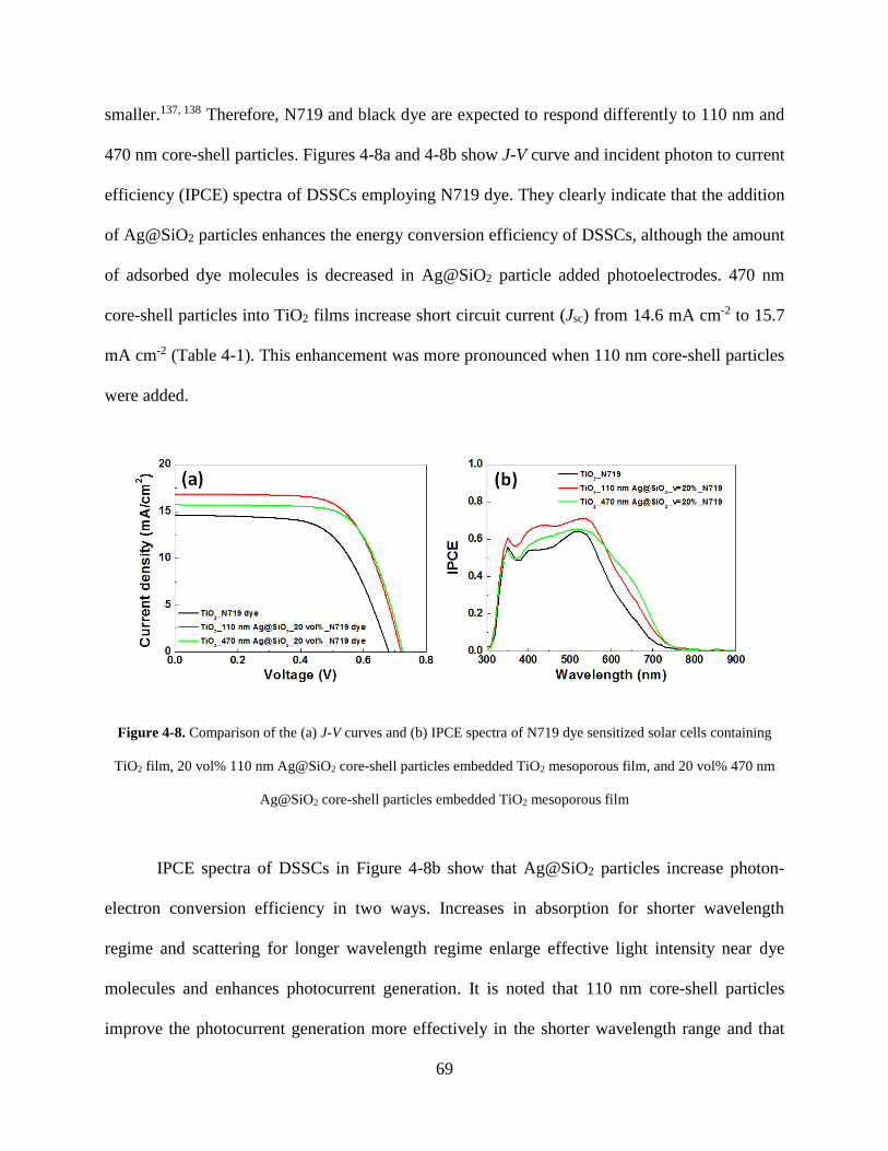
69
smaller.137, 138 Therefore, N719 and black dye are expected to respond differently to 110 nm and
470 nm core-shell particles. Figures 4-8a and 4-8b show J-V curve and incident photon to current
efficiency (IPCE) spectra of DSSCs employing N719 dye. They clearly indicate that the addition
of Ag@SiO2 particles enhances the energy conversion efficiency of DSSCs, although the amount
of adsorbed dye molecules is decreased in Ag@SiO2 particle added photoelectrodes. 470 nm
core-shell particles into TiO2 films increase short circuit current (Jsc) from 14.6 mA cm-2 to 15.7
mA cm-2 (Table 4-1). This enhancement was more pronounced when 110 nm core-shell particles
were added.
Figure 4-8. Comparison of the (a) J-V curves and (b) IPCE spectra of N719 dye sensitized solar cells containing
TiO2 film, 20 vol% 110 nm Ag@SiO2 core-shell particles embedded TiO2 mesoporous film, and 20 vol% 470 nm
Ag@SiO2 core-shell particles embedded TiO2 mesoporous film
IPCE spectra of DSSCs in Figure 4-8b show that Ag@SiO2 particles increase photon-
electron conversion efficiency in two ways. Increases in absorption for shorter wavelength
regime and scattering for longer wavelength regime enlarge effective light intensity near dye
molecules and enhances photocurrent generation. It is noted that 110 nm core-shell particles
improve the photocurrent generation more effectively in the shorter wavelength range and that

70
470 nm ones work better in longer wavelength range. At the wavelength of 650 nm, the
normalized IPCE is very dependent on the size of the Ag nanoshell. A difference in the
improvement of IPCE spectra by two kinds of core-shell particles agrees well with their different
spectral response shown in Figure 4-2. This indicates that a change in the geometric factor of the
core-shell particles can be used to tune the photon-electron conversion process of the solar cells.
Table 4-1. Photovoltaic performance of DSSCs based on different films with different dyes
Film Dye Voc (V) Jsc (mA/cm2) FF (%) PCE (%)
TiO2 N719 dye 0.68 14.6 63 6.2
TiO2/110 nm Ag@SiO2 N719 dye 0.72 16.8 67 8.1
TiO2/470 nm Ag@SiO2 N719 dye 0.73 15.7 69 7.9
TiO2/90 nm SiO2 N719 dye 0.72 11.6 70 5.9
TiO2/450 nm SiO2 N719 dye 0.70 12.3 71 6.1
TiO2 Black dye 0.63 7.4 72 3.4
TiO2/110 nm Ag@SiO2 Black dye 0.70 9.0 70 4.4
TiO2/470 nm Ag@SiO2 Black dye 0.70 11.7 72 5.9
Since 20 vol % of the composite film was occupied by large core-shell particles, the
surface area of the mixture film for dye absorption also almost 20% decreased. In order to show
the real improvement of the cell performance after employing core-shell particles, a control
experiment was conducted using composite films containing the same amount of bare silica
particles without silver layer coating. Both the J-V curve and IPCE show a dramatic decrease in
the cell performance (Figure 4-9), due to the decreased total surface area for dye absorption. This
indicates that it is mainly the plasmonic Ag nanoshell enhances the performance of DSSCs.
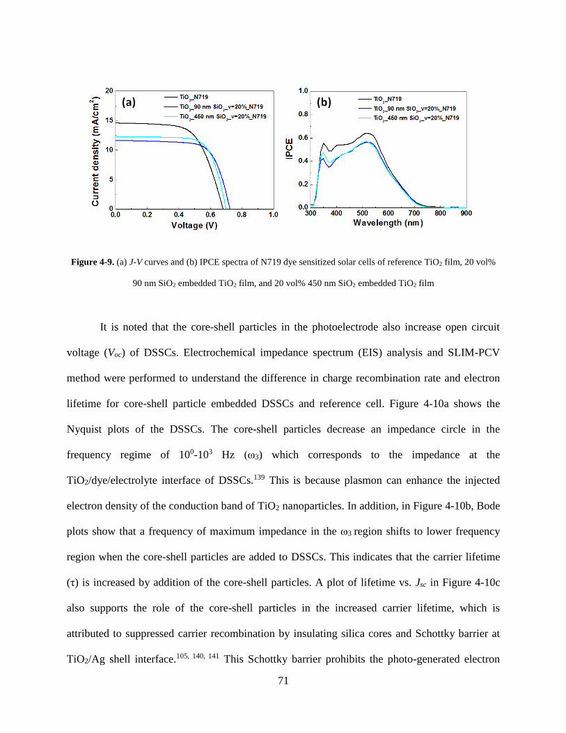
71
Figure 4-9. (a) J-V curves and (b) IPCE spectra of N719 dye sensitized solar cells of reference TiO2 film, 20 vol%
90 nm SiO2 embedded TiO2 film, and 20 vol% 450 nm SiO2 embedded TiO2 film
It is noted that the core-shell particles in the photoelectrode also increase open circuit
voltage (Voc) of DSSCs. Electrochemical impedance spectrum (EIS) analysis and SLIM-PCV
method were performed to understand the difference in charge recombination rate and electron
lifetime for core-shell particle embedded DSSCs and reference cell. Figure 4-10a shows the
Nyquist plots of the DSSCs. The core-shell particles decrease an impedance circle in the
frequency regime of 100-103 Hz (ω3) which corresponds to the impedance at the
TiO2/dye/electrolyte interface of DSSCs.139 This is because plasmon can enhance the injected
electron density of the conduction band of TiO2 nanoparticles. In addition, in Figure 4-10b, Bode
plots show that a frequency of maximum impedance in the ω3 region shifts to lower frequency
region when the core-shell particles are added to DSSCs. This indicates that the carrier lifetime
(τ) is increased by addition of the core-shell particles. A plot of lifetime vs. Jsc in Figure 4-10c
also supports the role of the core-shell particles in the increased carrier lifetime, which is
attributed to suppressed carrier recombination by insulating silica cores and Schottky barrier at
TiO2/Ag shell interface.105, 140, 141 This Schottky barrier prohibits the photo-generated electron

72
transferring from TiO2 to Ag nanoshell, so it can suppress the carrier trapping and recombination
by the silver nanoshell.
Figure 4-10. (a) Nyquist plots and (b) Bode plots of DSSCs with N719 dye. (c) Lifetime vs. Jsc plots of DSSCs with
N719 dye
The enhanced photon-electron conversion by the core-shell particles is more clearly
observed in black dye DSSCs. The light absorption ability of black dye molecules is smaller than
that of N719 dye, due to the low extinction coefficient and surface coverage of black dye.138
Therefore, the role of core-shell particles in light management is more critical in the light
harvesting of black dye DSSCs than N719 DSSCs. As shown in Figure 4-11a, Jsc of typical black
dye DSSCs increases from 7.4 mA cm-2 to 9.0 mA cm-2 when 110 nm core-shell particles are
added into TiO2 mesoporous films. The increase in Jsc is more dramatic when the same amount
of 470 nm core-shell particles is added. Jsc reaches 11.7 mA cm-2 in the core-shell particle added
black dye DSSCs (Table 4-1). Better performance of 470 nm core-shell particles in black dye
DSSCs is traced to the fact that the absorption and scattering spectra of larger core-shell particles
73
are pushed to longer wavelength range where black dye works better than N719 dye. Voc of the
core-shell particle embedded DSSCs is slightly larger than that of a control sample of pure TiO2
nanoparticle based DSSCs, which is similar to the core-shell particle added N719 dye. Given that
the addition of 20 vol% core-shell particles decreases the amount of adsorbed dye almost by 20%,
an increase in Jsc from 7.4 mA cm-2 to 11.7 mA cm-2 indicates that the core-shell particles of 470
nm can improve the cross section of black dye in DSSCs by a factor of two. In this high
efficiency DSSCs consisting of black dye and core-shell particles, aging or corrosion is
negligibly observed.
Figure 4-11b shows the IPCE spectra of black dye DSSCs. Both 110 nm and 470 nm
core-shell particles increase the photon-electron energy conversion efficiency. Compared with
110 nm particles, a uniform increase in IPCE is observed in the range of 500 nm to 800 nm
where larger core-shell particles cause higher scattering and absorption of incoming light. It
reveals that the enhanced photocurrent generation of black dye DSSCs is correlated to the
enhanced scattering and absorption by the core-shell particles. The performance of DSSCs using
black dye as the sensitizer exemplifies the benefit of the tuning capability of the Ag nanoshell.
Compared with N719, which is widely used in dye sensitized solar cells, the black dye has an
advantage of a broad light absorption spectrum. Black dye can collect more photons in red and
infrared light than N719 dye, which can increase the theoretical energy conversion efficiency of
the DSSCs. However, black dye has the critical problem of a small optical cross section and
weak surface coverage. Hence, DSSCs with black dye should employ a very thick
photoelectrode to absorb a large enough amount of solar light. The thick photoelectrode is likely
to prevent the electron transport, which, in turn, reduces the energy conversion efficiency of
DSSCs greatly below the theoretical limit. Results in Fig. 4-11 attest that the Ag nanoshell can

74
solve the problem of the small optical cross section of black dye and increase the theoretical limit
of DSSCs.
Figure 4-11. Comparison of the (a) J-V curves and (b) IPCE spectra of black dye sensitized solar cells containing
TiO2 film, 20 vol% 110 nm Ag@SiO2 core-shell particles embedded TiO2 mesoporous film, and 20 vol% 470 nm
Ag@SiO2 core-shell particles embedded TiO2 mesoporous film
75
5.0 DUAL PLASMON ASSISTED HIGH PERFORMANCE IN LEAD SULFIDE SOLAR
CELLS
5.1 BACKGROUND
Quantum Dots (QDs) have attracted a great deal of research interest over the past few decades
due to their unique optical and electronic properties.142 Their large optical cross section, tunable
band gap and slow phonon relaxation are valuable physical properties that are driving their use in
solar energy conversion devices, i.e., solar cells. In addition, QDs can be made through
inexpensive solution-based synthesis, and they are proving amenable to facile and large-scale
device fabrication methods. Hence, QDs have been used recently for different types of
photovoltaic devices.143 However, better device structures are needed for QD-based
photovoltaics to compete with the conventional technologies which are already commercialized.
QDs of lead chalcogenide , such as PbS and PbSe, have large Bohr exciton radius, low
exciton binding energy, and are considered excellent absorbers of visible and near IR light.144
Because of this promise, several groups have performed exploratory research to pave the way
toward creation of hybrid solar cells using p-type lead chalcogenide QDs as the photoactive
component of the solar cells.145 Moreover, QD solar cells have the potential of generating
multiple excitons from a single hot carrier, which is an inverse Auger type process.146, 147
76
Recently, the concept of multiple exciton generation (MEG) has been experimentally proven in a
thin-film type solar cell.148-151 The configuration of a so called thin-film type colloidal quantum
dots (CQDs) solar cell, as proposed by Sargent152-154 and Nozik,155, 156 contains a Schottky barrier
between a QDs semiconductor film and a metal thin film, where the photogenerated carriers are
collected.. From the standpoint of processing, this QD layer has the strength of easy deposition
using a spin coating process154, 157 or a layer-by-layer dip coating process.158 One main drawback
of the QD/metal structure is a low open circuit voltage (Voc), which is determined by the
separation of the quasi-Fermi levels at the contacts to the photoactive layer.159 To solve the
problem of low Voc, a layer of an n-type wide bandgap semiconductor such as TiO2159, 160 or ZnO
has been inserted between the QD layer and transparent conducting layer to form a depleted
heterojunction structure.161 This heterojunction changes the electron transport direction and
increases the quasi-Fermi level difference, leading to a higher Voc.159
In the thin-film type solar cells with Schottky junction and p-n junction, a tradeoff
between light absorption and carrier extraction is an important issue.162, 163 As the thickness of
the QD film increases to several hundreds of nanometer, the QD film can absorb more incoming
photons. However, since diffusion length of minority carrier becomes comparable to the QD film
thickness in a thick QD film, a probability for the carrier recombination increases and a charge
collection efficiency decreases.156 This shows an importance of increasing light absorption
without changing the QD layer thickness in heterojunction-type chalcogenide QD solar cells.
To date, many groups have worked on improving the energy conversion efficiency of
CQDs solar cells. For this purpose, the effect of the QD size on the injection and potential energy
of electrons has been investigated. One such group achieved optimum efficiency of the CQDs
solar cell by employing medium size PbS QDs with a band gap of 1.53 eV. Smaller QD
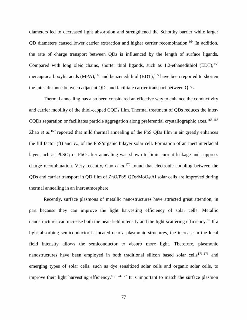
77
diameters led to decreased light absorption and strengthened the Schottky barrier while larger
QD diameters caused lower carrier extraction and higher carrier recombination.164 In addition,
the rate of charge transport between QDs is influenced by the length of surface ligands.
Compared with long oleic chains, shorter thiol ligands, such as 1,2-ethanedithiol (EDT),158
mercaptocarboxylic acids (MPA),160 and benzenedithiol (BDT),165 have been reported to shorten
the inter-distance between adjacent QDs and facilitate carrier transport between QDs.
Thermal annealing has also been considered an effective way to enhance the conductivity
and carrier mobility of the thiol-capped CQDs film. Thermal treatment of QDs reduces the inter-
CQDs separation or facilitates particle aggregation along preferential crystallographic axes.166-168
Zhao et al.169 reported that mild thermal annealing of the PbS QDs film in air greatly enhances
the fill factor (ff) and Voc of the PbS/organic bilayer solar cell. Formation of an inert interfacial
layer such as PbSO3 or PbO after annealing was shown to limit current leakage and suppress
charge recombination. Very recently, Gao et al.170 found that electronic coupling between the
QDs and carrier transport in QD film of ZnO/PbS QDs/MoOx/Al solar cells are improved during
thermal annealing in an inert atmosphere.
Recently, surface plasmons of metallic nanostructures have attracted great attention, in
part because they can improve the light harvesting efficiency of solar cells. Metallic
nanostructures can increase both the near-field intensity and the light scattering efficiency.65 If a
light absorbing semiconductor is located near a plasmonic structures, the increase in the local
field intensity allows the semiconductor to absorb more light. Therefore, plasmonic
nanostructures have been employed in both traditional silicon based solar cells171-173 and
emerging types of solar cells, such as dye sensitized solar cells and organic solar cells, to
improve their light harvesting efficiency.86, 174-177 It is important to match the surface plasmon

78
frequency with the light absorption spectrum of the photoactive materials. Thus different
metallic nanostructures have been studied, for example, nanoshells,30, 35, 178 nanocages,179, 180
nanoeggs181-183 and nanorods,184-186 because they provide tunable surface plasmons which are
exploited to improve the light absorption capability of photovoltaic devices.113, 133, 187, 188
Particularly, the plasmonic core-shell nanostructures, consisting of a silica sphere as the
dielectric core and a metal as the nanoshell, have been successfully utilized in PV devices such
as dye sensitized solar cells and QD solar cells.113, 136 Their unique surface plasmonic behavior
arises from the symmetric or anti-symmetric coupling of plasmons produced on the inner surface
and outer surface of the metal shell.39
Here, we employed plasmonic SiO2@Au@SiO2 (SGS) core-shell-shell particles to
enhance the photon-electron conversion efficiency in PbS QD thin film solar cells. The outer
silica layer, which overcoats the intermediate Au shell, enhances its chemical stability and
inhibits carrier trapping by the metal shell. In the plasmonic PbS QD solar cells, we
systematically studied the effect of the location of the plasmonic particles on the performance of
PbS QD heterojunction-type thin film solar cells (fluorine doped SnO2 (FTO) /TiO2/PbS/Au)
from the standpoint of light absorption enhancement. For this purpose, we chose two different
designs with the SGSs placed either at the PbS-Au interface or the PbS-TiO2 interface. We found
that a dual enhancement was achieved for the devices with the SGSs at the PbS-TiO2 interface
because it causes nanodome structures to form on the top Au electrode.
5.1.1 PbS QDs and Surface Ligands
Comparing with the first excitonic transition peak at λ = 3200 nm for bulk PbS (Eg = 0.41 eV),
the first excitonic transition of the PbS QDs, whose average diameter is less than 10 nm, can

79
reach to near IR or visible regime. Then a strong quantum confinement will be realized due to a
large Bohr radius (18 nm) of the PbS. The PbS QDs can be prepared by a classical procedure
developed by Hines and Scholes,144 in which the long oleic chain is used as the passivation layer
for size and stability control. Typical morphology of the PbS QDs with an average diameter of
6.5 nm is shown in Figure 5-1a. The first excitonic absorption of the PbS QDs can be readily
tuned from 800 nm to 1700 nm as the diameter of the particle increases from 3 nm to 7 nm (Fig.
5-1b).144, 164
Figure 5-1. (a) HRTEM images of colloidal PbS QDs with an average diameter of 6.5 nm. (b) Optical
characterization of toluene solutions of oleic acid capped PbS QDs 144
Surface ligands play an important role in colloidal QDs synthesis, since they control the
nanoparticle nucleation, growth and surface passivation. In addition, surface ligand is a key
factor for assembling individual particles into ordered NC solid and film. So far, four types of
ligands have been widely utilized in nanocrystal preparation, such as molecules with single head
group and a long hydrocarbon chain, short-chain molecules with single head group, cross-linking
molecules with two end groups and metal chalcogenide complexes (Figure 5-2).142

80
Figure 5-2. Different Types of Surface Ligands Used in Nanocrystals and Nanocrystal Solids 142
Surface ligand with a long organic chain can passivate the charged surface of the
nanoparticles and prohibit particle agglomeration and precipitation in the solution. However, it
acts as bulky insulating barrier and hinders the inter-particle charge transportation. On the other
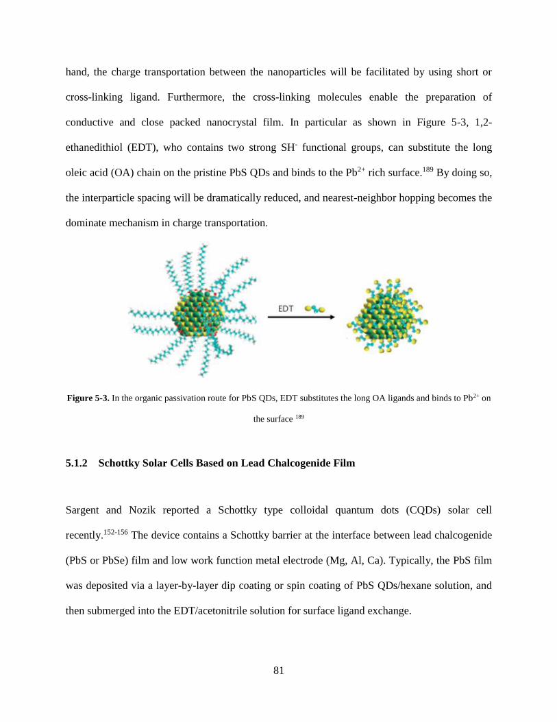
81
hand, the charge transportation between the nanoparticles will be facilitated by using short or
cross-linking ligand. Furthermore, the cross-linking molecules enable the preparation of
conductive and close packed nanocrystal film. In particular as shown in Figure 5-3, 1,2-
ethanedithiol (EDT), who contains two strong SH- functional groups, can substitute the long
oleic acid (OA) chain on the pristine PbS QDs and binds to the Pb2+ rich surface.189 By doing so,
the interparticle spacing will be dramatically reduced, and nearest-neighbor hopping becomes the
dominate mechanism in charge transportation.
Figure 5-3. In the organic passivation route for PbS QDs, EDT substitutes the long OA ligands and binds to Pb2+ on
the surface 189
5.1.2 Schottky Solar Cells Based on Lead Chalcogenide Film
Sargent and Nozik reported a Schottky type colloidal quantum dots (CQDs) solar cell
recently.152-156 The device contains a Schottky barrier at the interface between lead chalcogenide
(PbS or PbSe) film and low work function metal electrode (Mg, Al, Ca). Typically, the PbS film
was deposited via a layer-by-layer dip coating or spin coating of PbS QDs/hexane solution, and
then submerged into the EDT/acetonitrile solution for surface ligand exchange.
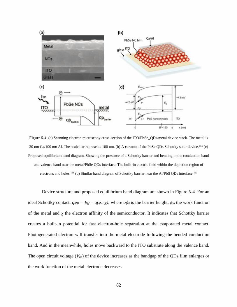
82
Figure 5-4. (a) Scanning electron microscopy cross-section of the ITO/PbSe_QDs/metal device stack. The metal is
20 nm Ca/100 nm Al. The scale bar represents 100 nm. (b) A cartoon of the PbSe QDs Schottky solar device.155 (c)
Proposed equilibrium band diagram. Showing the presence of a Schottky barrier and bending in the conduction band
and valence band near the metal/PbSe QDs interface. The built-in electric field within the depletion region of
electrons and holes.156 (d) Similar band diagram of Schottky barrier near the Al/PbS QDs interface 163
Device structure and proposed equilibrium band diagram are shown in Figure 5-4. For an
ideal Schottky contact, qϕB = Eg – q(ϕm-χ), where qϕB is the barrier height, ϕm the work function
of the metal and χ the electron affinity of the semiconductor. It indicates that Schottky barrier
creates a built-in potential for fast electron-hole separation at the evaporated metal contact.
Photogenerated electron will transfer into the metal electrode following the bended conduction
band. And in the meanwhile, holes move backward to the ITO substrate along the valence band.
The open circuit voltage (Voc) of the device increases as the bandgap of the QDs film enlarges or
the work function of the metal electrode decreases.

83
Mott-Schottky analysis permits a determination of depletion width, built-in potential and
carrier concentration in the semiconductor film. The depletion width (W) of the Schottky
junction is equal to
(5-1)
where ɛ is the static dielectric constant of the QDs film, ɛ0 the permittivity of the free
space, ϕbi the built-in potential, V the applied bias, and N the carrier concentration at the edge of
the depletion layer. In addition, N can be calculated from the equation
(5-2)
where C is the capacitance of the depletion region and can be measured from the Mott-
Schottky plots (1/C2 vs. Voltage).
Time-of-flight technique (Figure 5-5a,b) can be applied to obtain the electron mobility
and transient open circuit voltage decay (OCVD) to measure the recombination-limited lifetime
of carriers (Figure 5-5c,d).
84
Figure 5-5. Current transient signals used to extract (a) the hole mobility (CELIV, 80000 V s-1 ramp rate) and (b)
the electron mobility (time-of-flight, under 40 V bias). (c) Voc decay signal (after 975 nm, 16 mW cm-2 illumination
turn off) and a linear best fit (dashed red line) used to determine the recombination-llimited lifetime. (d) Lifetime
(blue crosses, left axis) and EQE (red circles, right axis) and as a function of illumination intensity at 975 nm 163
The time-of-flight transients were obtained by illuminating the ITO/PbS QD film/Al
device with a 10 ns pulse at 532 nm using an yttrium aluminum garnet laser. To isolate the
electron transport dynamics, devices were reverse biased. The obtained electron mobility in the
fully depleted region was (2 ± 1) × 10-4 cm2 V-1 s-1.163 For the OCVD measurement, the ITO/PbS
QD film/Al device was illuminated by a 975 nm diode laser, modulated using a digital pulse

85
generator, at room temperature. Immediately after turn off the laser, an initial slope of the decay
(dVoc/dt) is related to the lifetime (τ) by
(5-3)
where k is the Boltzman constant, T the temperature, q the elementary charge and F1
ranges between 1 at low injection and 2 at high injection. Measured lifetime of PbS and PbSe
QDs reveals that the lifetime increases steadily from ~ 10 µs at high light intensities to 1 ms at
low light intensities.163 The drift length of the carriers is given by . By
calculation, at 12 mW cm-2, the hole and electron drift length in ITO/PbS QD film/Al device is
of 10 and 1 µm,163 which are far longer than the depletion width (~ 150 nm).
Thus, the efficiency of the Schottky device depends on the balance between light
absorption and carrier extraction. In the device with a thick photosensitizer layer, efficiency is
limited by the rate of the carrier diffusion through the neutral region. Although thicker PbS QDs
layer can absorb more photons for carrier generation, however, carriers have a higher
recombination chance when transporting to the opposite contact. As a result, ~ 230 nm is the
optimized thickness of PbS QDs film in the Schottky-type solar device.
5.1.3 Heterojunction Solar Cells Based on PbS QDs Film
By inserting another n-type semiconductor film with wide bandgap, such as TiO2 and ZnO,
between the PbS QDs and metal electrode, another planar heterojunction will be introduced into
the Shottky solar device, if the metal electrode is substituted by high work function metal, like
Au or Ag. This planar heterojunction will change the carrier transportation directions and a so-
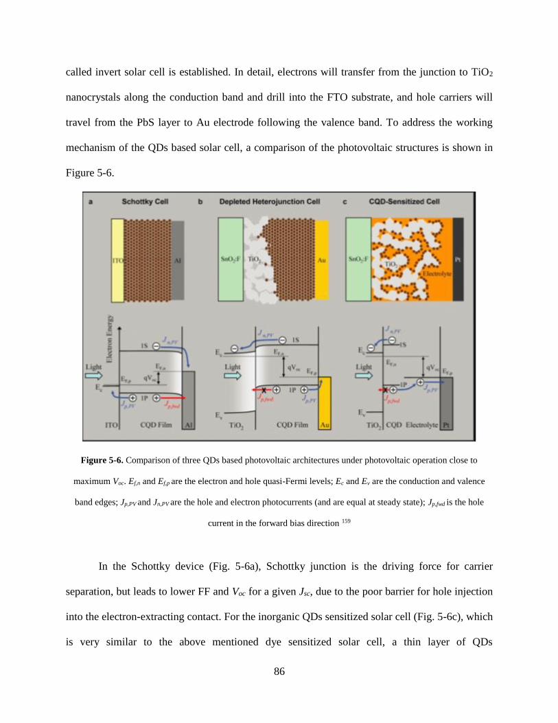
86
called invert solar cell is established. In detail, electrons will transfer from the junction to TiO2
nanocrystals along the conduction band and drill into the FTO substrate, and hole carriers will
travel from the PbS layer to Au electrode following the valence band. To address the working
mechanism of the QDs based solar cell, a comparison of the photovoltaic structures is shown in
Figure 5-6.
Figure 5-6. Comparison of three QDs based photovoltaic architectures under photovoltaic operation close to
maximum Voc. Ef,n and Ef,p are the electron and hole quasi-Fermi levels; Ec and Ev are the conduction and valence
band edges; Jp,PV and Jn,PV are the hole and electron photocurrents (and are equal at steady state); Jp,fwd is the hole
current in the forward bias direction 159
In the Schottky device (Fig. 5-6a), Schottky junction is the driving force for carrier
separation, but leads to lower FF and Voc for a given Jsc, due to the poor barrier for hole injection
into the electron-extracting contact. For the inorganic QDs sensitized solar cell (Fig. 5-6c), which
is very similar to the above mentioned dye sensitized solar cell, a thin layer of QDs
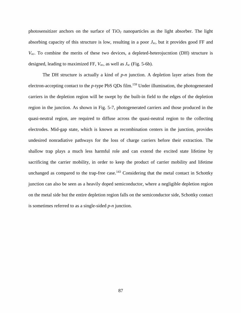
87
photosensitizer anchors on the surface of TiO2 nanoparticles as the light absorber. The light
absorbing capacity of this structure is low, resulting in a poor Jsc, but it provides good FF and
Voc. To combine the merits of these two devices, a depleted-heterojucntion (DH) structure is
designed, leading to maximized FF, Voc, as well as Jsc (Fig. 5-6b).
The DH structure is actually a kind of p-n junction. A depletion layer arises from the
electron-accepting contact to the p-type PbS QDs film.159 Under illumination, the photogenerated
carriers in the depletion region will be swept by the built-in field to the edges of the depletion
region in the junction. As shown in Fig. 5-7, photogenerated carriers and those produced in the
quasi-neutral region, are required to diffuse across the quasi-neutral region to the collecting
electrodes. Mid-gap state, which is known as recombination centers in the junction, provides
undesired nonradiative pathways for the loss of charge carriers before their extraction. The
shallow trap plays a much less harmful role and can extend the excited state lifetime by
sacrificing the carrier mobility, in order to keep the product of carrier mobility and lifetime
unchanged as compared to the trap-free case.143 Considering that the metal contact in Schottky
junction can also be seen as a heavily doped semiconductor, where a negligible depletion region
on the metal side but the entire depletion region falls on the semiconductor side, Schottky contact
is sometimes referred to as a single-sided p-n junction.

88
Figure 5-7. Schematic diagram of a p-n junction. qVoc is the difference between the quasi-Fermi level Fn of
electrons in the n-type material and quasi-Fermi level Fp of holes in the p-type material under illumination. Mid-gap
states and shallow traps are present in both the p- and n-type materials 143
Figure 5-8 shows the energy level of the TiO2 and PbS QDs with various sizes. It
indicates that as the QDs size grows, the first excitonic absorption shifts red and a wider solar
spectrum will be covered, leading to an expected higher Jsc. But the as-narrowed bandgap of the
QDs will cause continuous decrease of Voc. A clear cross-section view of the device is shown in
a TEM image (Fig. 5-8c) and each layer was characterized by the energy dispersive X-ray
analysis.
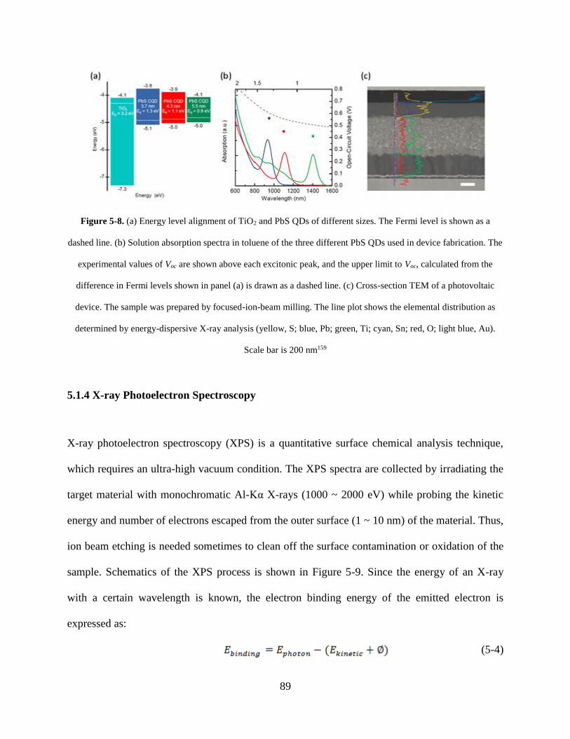
89
Figure 5-8. (a) Energy level alignment of TiO2 and PbS QDs of different sizes. The Fermi level is shown as a
dashed line. (b) Solution absorption spectra in toluene of the three different PbS QDs used in device fabrication. The
experimental values of Voc are shown above each excitonic peak, and the upper limit to Voc, calculated from the
difference in Fermi levels shown in panel (a) is drawn as a dashed line. (c) Cross-section TEM of a photovoltaic
device. The sample was prepared by focused-ion-beam milling. The line plot shows the elemental distribution as
determined by energy-dispersive X-ray analysis (yellow, S; blue, Pb; green, Ti; cyan, Sn; red, O; light blue, Au).
Scale bar is 200 nm159
5.1.4 X-ray Photoelectron Spectroscopy
X-ray photoelectron spectroscopy (XPS) is a quantitative surface chemical analysis technique,
which requires an ultra-high vacuum condition. The XPS spectra are collected by irradiating the
target material with monochromatic Al-Kα X-rays (1000 ~ 2000 eV) while probing the kinetic
energy and number of electrons escaped from the outer surface (1 ~ 10 nm) of the material. Thus,
ion beam etching is needed sometimes to clean off the surface contamination or oxidation of the
sample. Schematics of the XPS process is shown in Figure 5-9. Since the energy of an X-ray
with a certain wavelength is known, the electron binding energy of the emitted electron is
expressed as:
(5-4)
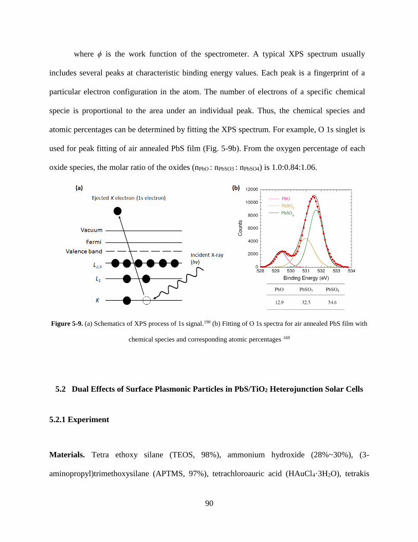
90
where ϕ is the work function of the spectrometer. A typical XPS spectrum usually
includes several peaks at characteristic binding energy values. Each peak is a fingerprint of a
particular electron configuration in the atom. The number of electrons of a specific chemical
specie is proportional to the area under an individual peak. Thus, the chemical species and
atomic percentages can be determined by fitting the XPS spectrum. For example, O 1s singlet is
used for peak fitting of air annealed PbS film (Fig. 5-9b). From the oxygen percentage of each
oxide species, the molar ratio of the oxides (nPbO : nPbSO3 : nPbSO4) is 1.0:0.84:1.06.
Figure 5-9. (a) Schematics of XPS process of 1s signal.190 (b) Fitting of O 1s spectra for air annealed PbS film with
chemical species and corresponding atomic percentages 169
5.2 Dual Effects of Surface Plasmonic Particles in PbS/TiO2 Heterojunction Solar Cells
5.2.1 Experiment
Materials. Tetra ethoxy silane (TEOS, 98%), ammonium hydroxide (28%~30%), (3-
aminopropyl)trimethoxysilane (APTMS, 97%), tetrachloroauric acid (HAuCl4·3H2O), tetrakis
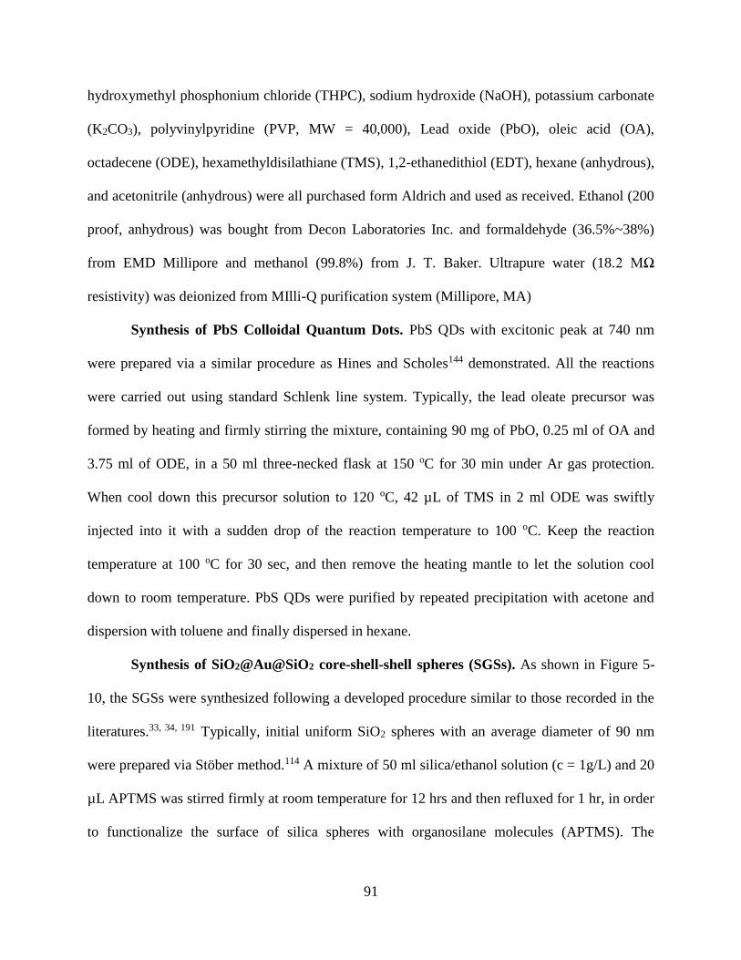
91
hydroxymethyl phosphonium chloride (THPC), sodium hydroxide (NaOH), potassium carbonate
(K2CO3), polyvinylpyridine (PVP, MW = 40,000), Lead oxide (PbO), oleic acid (OA),
octadecene (ODE), hexamethyldisilathiane (TMS), 1,2-ethanedithiol (EDT), hexane (anhydrous),
and acetonitrile (anhydrous) were all purchased form Aldrich and used as received. Ethanol (200
proof, anhydrous) was bought from Decon Laboratories Inc. and formaldehyde (36.5%~38%)
from EMD Millipore and methanol (99.8%) from J. T. Baker. Ultrapure water (18.2 MΩ
resistivity) was deionized from MIlli-Q purification system (Millipore, MA)
Synthesis of PbS Colloidal Quantum Dots. PbS QDs with excitonic peak at 740 nm
were prepared via a similar procedure as Hines and Scholes144 demonstrated. All the reactions
were carried out using standard Schlenk line system. Typically, the lead oleate precursor was
formed by heating and firmly stirring the mixture, containing 90 mg of PbO, 0.25 ml of OA and
3.75 ml of ODE, in a 50 ml three-necked flask at 150 oC for 30 min under Ar gas protection.
When cool down this precursor solution to 120 oC, 42 µL of TMS in 2 ml ODE was swiftly
injected into it with a sudden drop of the reaction temperature to 100 oC. Keep the reaction
temperature at 100 oC for 30 sec, and then remove the heating mantle to let the solution cool
down to room temperature. PbS QDs were purified by repeated precipitation with acetone and
dispersion with toluene and finally dispersed in hexane.
Synthesis of SiO2@Au@SiO2 core-shell-shell spheres (SGSs). As shown in Figure 5-
10, the SGSs were synthesized following a developed procedure similar to those recorded in the
literatures.33, 34, 191 Typically, initial uniform SiO2 spheres with an average diameter of 90 nm
were prepared via Stöber method.114 A mixture of 50 ml silica/ethanol solution (c = 1g/L) and 20
µL APTMS was stirred firmly at room temperature for 12 hrs and then refluxed for 1 hr, in order
to functionalize the surface of silica spheres with organosilane molecules (APTMS). The
92
functionalized silica spheres were centrifuged and redispersed in pure ethanol several times to
remove the excess APTMS. Aqueous solution of tiny gold nanoparticles with a diameter of ~2
nm were prepared via Duff’s method,192 and further diluted to 100 ml. The as formed
silica/ethanol solution was concentrated to 25 ml, and drop by drop added to this rapidly stirred
gold aqueous solution. After stirring for 12 hrs at room temperature, non-attached gold
nanoparticles were removed by centrifugation, leaving behind silica spheres decorated with gold
nanoparticles through the gold-amine interactions. These attached gold seeds played the role of
nucleation sites for further gold shell growth.
Figure 5-10. Seed mediated procedure of SiO2@Au@SiO2 particle fabrication, which includes three steps of (a)
SiO2 core, (b) Au@SiO2 and (c) SiO2@Au@SiO2 preparation
93
Au plating solution was prepared by adding 17.1 mg (25 mM) HAuCl4·3H2O and 124.5
mg (1.8 mM) of K2CO3 into 100 ml deionized water, and after aging 2 days, seeded silica
aqueous solution was dropped in it with vigorous stirring at room temperature. The AuCl− ions
reduction started after 200 µL of formaldehyde was added to the mixture, and complete gold
nanoshell with a thickness of 20 nm was formed within 20 min. In order to coat another silica
shell out of the Au@SiO2 particles (GSs), no purification was needed to the pristine GSs aqueous
solution, and 10 ml of 0.5 mM PVP aqueous solution was immediately added once the GSs were
formed. After stirring for another 24 hrs, the PVP stabilized GSs were centrifuged and purified in
deionized water and ethanol several times. Resulting particles were redispersed in 194 ml of pure
ethanol, with subsequently adding 8.5 ml of ammonium hydroxide and 0.9 ml of TEOS solution
(10 vol% in pure ethanol). This mixture was then stirred for 12 hrs at room temperature to form
SGSs. Final product was washed by pure ethanol and restored in methol.
Device Fabrication. Patterned fluorine-doped tin oxide (FTO) (Pilington TEC 8) coated
glass substrates were cleaned by merging in ethanol/acetone (1:1) mixture under sonication for
10 min. TiO2 sol made of TTIP acidic solution was spin coated on the precleaned FTO and
subsequently annealed in O2 at 500 oC for 2 hrs, resulting in a 80 nm hole blocking layer. Then
TiO2 paste, composed of TiO2 nanoparticles with a diameter of ~ 20 nm and prepared via a
hydrothermal reaction, was printed on the blocking layer by a doctor blading method. After
annealing at 450 oC for 30 min under N2 gas protection, a second TiO2 film formed with a
thickness of ~ 1µm. In order to build a planar heterojunction for carrier separation, on top of this
TiO2 mesoporous film, PbS QD film was prepared by a layer-by-layer dip coating method in an
Ar gas filled glove box. Typically, the substrate with TiO2 film was merged into PbS
QDs/hexane solution (20 mg/ml) by hand, and after 5 sec, slowly dragged out of the solution at a
94
velocity of ~0.2 cm s-1. Subsequently, it was re-dipped into 0.1 M EDT/acetonitrile for 10 sec
and quickly removed. This dipping procedure was repeated 14 times, resulting in a 150 nm close
packed PbS film. In order to locate the SGSs on top of the PbS film or inside of the film, a
monolayer of SGSs, which covers ~ 20 % area of the substrate, was drop coated in the device
after and before the PbS deposition separately from a diluted SGSs/methanol solution, and
loosely attached particles were then washed away by methanol after solvent evaporated
naturally. Similarly, SiO2 spheres, whose average diameter is of 150 nm and prepared by the
Stöber method as well, were drop coated on the TiO2 film as a control sample. Finally, 20 nm
thick gold layer was deposited onto the PbS film by electron beam evaporation as the top
electrode. Each device has an active area of 0.04 cm2.
PbS QDs, PbS film, GSs and SGSs Characterization. The morphologies of the GSs,
SGSs, PbS QDs and cross-section view of the Au/PbS/TiO2 films were tested by high-resolution
electron microscopy (HRTEM, JEOL JEM-2100F). The Z-contrast high angle annular dark field
(HADDF) cross-section images of the films were tested in STEM mode. And the element
distribution was studied with EDS mapping. The PbS QD sample was prepared on a Cu grid,
with a post ligand exchange in 0.1 M EDT/acetonitrile solution for 10 sec. The film sample was
deposited on silicon substrate and prepared by mechanical polishing and ion milling. The optical
properties of the GSs, SGSs, PbS QDs and PbS film were investigated with the UV-vis
spectrophotometer (Lambda 35, Perkin Elmer) attached to an integrating sphere ranging from
300 nm to 1100 nm. X-ray photoelectron spectra (XPS) were collected with monochromatic Al-
Kα X-rays (1487 eV) at 150W power on a custom built multi-technique surface analysis
instrument. In order to increase the accuracy and sensitivity of the analysis, surface
contamination or oxidation of the PbS films were cleaned off by ion beam etching before signal
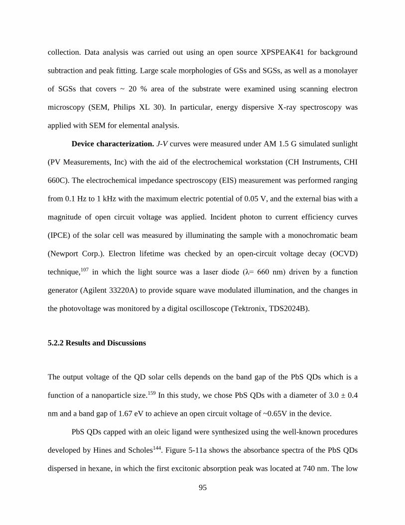
95
collection. Data analysis was carried out using an open source XPSPEAK41 for background
subtraction and peak fitting. Large scale morphologies of GSs and SGSs, as well as a monolayer
of SGSs that covers ~ 20 % area of the substrate were examined using scanning electron
microscopy (SEM, Philips XL 30). In particular, energy dispersive X-ray spectroscopy was
applied with SEM for elemental analysis.
Device characterization. J-V curves were measured under AM 1.5 G simulated sunlight
(PV Measurements, Inc) with the aid of the electrochemical workstation (CH Instruments, CHI
660C). The electrochemical impedance spectroscopy (EIS) measurement was performed ranging
from 0.1 Hz to 1 kHz with the maximum electric potential of 0.05 V, and the external bias with a
magnitude of open circuit voltage was applied. Incident photon to current efficiency curves
(IPCE) of the solar cell was measured by illuminating the sample with a monochromatic beam
(Newport Corp.). Electron lifetime was checked by an open-circuit voltage decay (OCVD)
technique,107 in which the light source was a laser diode (λ= 660 nm) driven by a function
generator (Agilent 33220A) to provide square wave modulated illumination, and the changes in
the photovoltage was monitored by a digital oscilloscope (Tektronix, TDS2024B).
5.2.2 Results and Discussions
The output voltage of the QD solar cells depends on the band gap of the PbS QDs which is a
function of a nanoparticle size.159 In this study, we chose PbS QDs with a diameter of 3.0 ± 0.4
nm and a band gap of 1.67 eV to achieve an open circuit voltage of ~0.65V in the device.
PbS QDs capped with an oleic ligand were synthesized using the well-known procedures
developed by Hines and Scholes144. Figure 5-11a shows the absorbance spectra of the PbS QDs
dispersed in hexane, in which the first excitonic absorption peak was located at 740 nm. The low
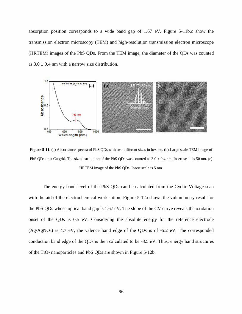
96
absorption position corresponds to a wide band gap of 1.67 eV. Figure 5-11b,c show the
transmission electron microscopy (TEM) and high-resolution transmission electron microscope
(HRTEM) images of the PbS QDs. From the TEM image, the diameter of the QDs was counted
as 3.0 ± 0.4 nm with a narrow size distribution.
Figure 5-11. (a) Absorbance spectra of PbS QDs with two different sizes in hexane. (b) Large scale TEM image of
PbS QDs on a Cu grid. The size distribution of the PbS QDs was counted as 3.0 ± 0.4 nm. Insert scale is 50 nm. (c)
HRTEM image of the PbS QDs. Insert scale is 5 nm.
The energy band level of the PbS QDs can be calculated from the Cyclic Voltage scan
with the aid of the electrochemical workstation. Figure 5-12a shows the voltammetry result for
the PbS QDs whose optical band gap is 1.67 eV. The slope of the CV curve reveals the oxidation
onset of the QDs is 0.5 eV. Considering the absolute energy for the reference electrode
(Ag/AgNO3) is 4.7 eV, the valence band edge of the QDs is of -5.2 eV. The corresponded
conduction band edge of the QDs is then calculated to be -3.5 eV. Thus, energy band structures
of the TiO2 nanoparticles and PbS QDs are shown in Figure 5-12b.
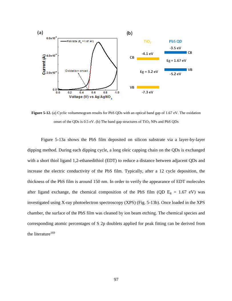
97
Figure 5-12. (a) Cyclic voltammogram results for PbS QDs with an optical band gap of 1.67 eV. The oxidation
onset of the QDs is 0.5 eV. (b) The band gap structures of TiO2 NPs and PbS QDs
Figure 5-13a shows the PbS film deposited on silicon substrate via a layer-by-layer
dipping method. During each dipping cycle, a long oleic capping chain on the QDs is exchanged
with a short thiol ligand 1,2-ethanedithiol (EDT) to reduce a distance between adjacent QDs and
increase the electric conductivity of the PbS film. Typically, after a 12 cycle deposition, the
thickness of the PbS film is around 150 nm. In order to verify the appearance of EDT molecules
after ligand exchange, the chemical composition of the PbS film (QD Eg = 1.67 eV) was
investigated using X-ray photoelectron spectroscopy (XPS) (Fig. 5-13b). Once loaded in the XPS
chamber, the surface of the PbS film was cleaned by ion beam etching. The chemical species and
corresponding atomic percentages of S 2p doublets applied for peak fitting can be derived from
the literature169
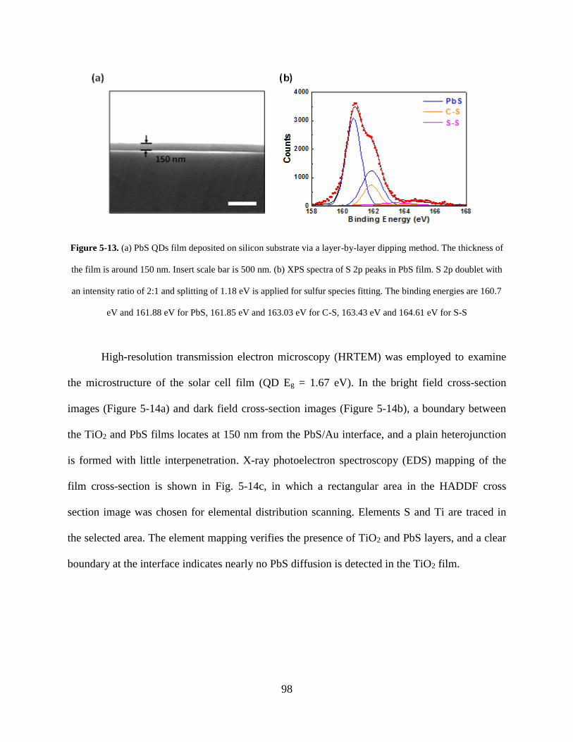
98
Figure 5-13. (a) PbS QDs film deposited on silicon substrate via a layer-by-layer dipping method. The thickness of
the film is around 150 nm. Insert scale bar is 500 nm. (b) XPS spectra of S 2p peaks in PbS film. S 2p doublet with
an intensity ratio of 2:1 and splitting of 1.18 eV is applied for sulfur species fitting. The binding energies are 160.7
eV and 161.88 eV for PbS, 161.85 eV and 163.03 eV for C-S, 163.43 eV and 164.61 eV for S-S
High-resolution transmission electron microscopy (HRTEM) was employed to examine
the microstructure of the solar cell film (QD Eg = 1.67 eV). In the bright field cross-section
images (Figure 5-14a) and dark field cross-section images (Figure 5-14b), a boundary between
the TiO2 and PbS films locates at 150 nm from the PbS/Au interface, and a plain heterojunction
is formed with little interpenetration. X-ray photoelectron spectroscopy (EDS) mapping of the
film cross-section is shown in Fig. 5-14c, in which a rectangular area in the HADDF cross
section image was chosen for elemental distribution scanning. Elements S and Ti are traced in
the selected area. The element mapping verifies the presence of TiO2 and PbS layers, and a clear
boundary at the interface indicates nearly no PbS diffusion is detected in the TiO2 film.
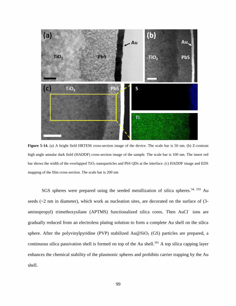
99
Figure 5-14. (a) A bright field HRTEM cross-section image of the device. The scale bar is 50 nm. (b) Z-contrast
high angle annular dark field (HADDF) cross-section image of the sample. The scale bar is 100 nm. The insert red
bar shows the width of the overlapped TiO2 nanoparticles and PbS QDs at the interface. (c) HADDF image and EDS
mapping of the film cross-section. The scale bar is 200 nm
SGS spheres were prepared using the seeded metallization of silica spheres.34, 193 Au
seeds (~2 nm in diameter), which work as nucleation sites, are decorated on the surface of (3-
aminopropyl) trimethoxysilane (APTMS) functionalized silica cores. Then AuCl− ions are
gradually reduced from an electroless plating solution to form a complete Au shell on the silica
sphere. After the polyvinylpyridine (PVP) stabilized Au@SiO2 (GS) particles are prepared, a
continuous silica passivation shell is formed on top of the Au shell.191 A top silica capping layer
enhances the chemical stability of the plasmonic spheres and prohibits carrier trapping by the Au
shell.
100
Based on preliminary results, SGSs which consist of a silica core with 90 nm diameter,
20 nm gold intermediate layer, and 7 nm outer silica shell were chosen as the plasmon
contributor, since they exhibit increased light absorption and scattering at 600 nm ~ 1000 nm
where PbS QDs with a bandgap of 1.67 eV need field-enhancement effect for better light
harvesting. The outer silica shell was thinner than 10 nm to minimize a change in the near-field
intensity at the outer silica shell.194 The large scale morphologies of the GSs and SGSs were
tested by SEM (Figure 5-15a,b). It indicates that the GSs and SGSs are uniform sub-
microspheres with a diameter of 130 ± 10 nm and 144 ± 10 nm, respectively. In order to
investigate the component of the spheres, EDS test was applied to detect the elemental
information on the whole area as that shown in the SEM image. In particular, Figure 5-15c
shows the element analysis of GSs, where strong Au peak corresponds to the Au nanoshells, and
Si and O peaks are related to the inner silica cores. Otherwise, Figure 5-16d shows the result for
SGSs, in which the signals of Si and O are enhanced comparatively, due to another outer silica
shell coating.

101
Figure 5-15. (a) Large scale SEM images of GSs, with (c) elemental analysis on the same whole area by EDS. (b)
Large scale SEM images of SGSs, with (b) relevant EDS test on the same whole area. Inset scale bar is 1 µm
Figure 5-16a-c shows transmission electron microscopy (TEM) images of the
morphology evolution of these SGSs from bare silica spheres (~90 nm in diameter) to final core-
shell-shell particles. Typically, the Au shell is ~ 20 nm thick and outer silica shell is ~7 nm. The
high resolution TEM (HRTEM) image in Figure 1d shows a d-spacing between atomic layers of
2.35Å which corresponds to the (111) plane of Au. The thin outer silica shell is designed to
separate direct contact between Au shell and PbS QDs in the device, in order to prohibit carrier
trapping and recombination at the Au shell. The optical properties of GSs and SGSs were
measured by UV-vis spectrometer (Fig. 5-16e). Their main plasmon peaks locate at 660 nm and
680 nm, respectively. The red-shift of the plasmon peak from GS to SGS is due to a slight

102
change in a dielectric constant of media after the outer silica shell was coated. Compared to
water or air, silica has a higher dielectric constant, which decreases the plamonic frequency of
embedded metallic nanostructures.
Figure 5-16. Morphology evolution of the SGSs. (a) bare silica spheres with a diameter of ~ 90 nm. (b) Au@SiO2
core-shell particles with an Au shell of ~20 nm thick. (c) SGSs with another outer silica shell of ~7 nm thick. Insert
scale bar in (a-c) is 100 nm. (d) The HRTEM of the Au nanoshell. The d-spacing of 2.35 Å corresponds to the (111)
plane of Au. (e) Absorbance spectra of GSs and SGSs dispersed in deionized water
Figure 5-17 shows the schematics of the device structures. A controlled solar cell without
the plasmonic particles consists of four layers deposited on FTO coated glass substrate: 80 nm
thick TiO2 hole blocking layer, 1 µm thick TiO2 mesoporous film, 150 nm thick PbS QDs film
and 20 nm thick Au electrode. In principle, PbS film acts as light absorber and hole

103
transportation layer, and TiO2 film works as the electron transportation layer. The energy level
diagram of the device is illustrated in Figure 5-17e. The electron is injected from the conduction
band of PbS QDs to that of TiO2 and moves to FTO, and the hole path is formed from the
valance band of PbS QDs to the valence band of Au anode. A built-in potential at the TiO2/PbS
interface promotes electron-hole separation and carrier injection.
To investigate the dual effect of the plasmonic particles on the performance of thin film
solar cells, plasmonic SGSs are added into the devices in two different ways (Figure 5-17b,c).
One is to coat a monolayer of SGSs on top of the PbS film via a dip coating before Au electrode
deposition, and the other is to place the SGSs on TiO2 film first and coat the PbS film on SGS
decorated TiO2 film. In the latter case, SGSs covers 20% of FTO surface. Figure 5-17f shows the
distribution of SGSs on the substrate before the dip coating of PbS QDs. SGSs cover 20% of the
surface area and an average distance between adjacent SGSs is about 400 nm. These two
different structures are expected to manage incoming light differently. SGSs on the top of the
PbS QD film are intended couple LSPRs with photons after light passes through PbS film. An
advantage of this design is to minimize energy dissipation at the Au shell, since photons hit PbS
film first. On the other hand, SGSs between the PbS film and TiO2 film cause a dual effect. In
this configuration, SGSs at the bottom increases the near-field intensity and nanodomes formed
on the top Au layer induce additional light scattering and near-field enhancement effects.

104
Figure 5-17. Device architectures with cross-section view of the SEM images. (a) Standard sample without SGSs,
(b) device with SGSs embedded between the PbS film and Au anode (SGS on top), (c) SGSs merged in PbS film
(SGS inside) and (d) SiO2 spheres merged in PbS film (SiO2 inside). The insert scale bar is 200 nm. (e) Energy level
diagram of the standard device. (f) SEM image of a monolayer of SGSs prepared by spin coating and covering the
surface area of a substrate by ~ 20 %. Scale bar is 2 µm
A theoretical simulation predicts that the second nanodome effect facilitates additional
light absorption in the wavelength range of 500 nm ~ 800 nm.174 Though this geometry causes
small light absorption in a front end of the device, the plasmonic particles and nanodomes

105
located at both interfaces of PbS films may compensate light loss and creates a synergistic effect.
In order to investigate a pure effect of the nanodomes on the top surface of Au electrode, bare
silica spheres with an average diameter of 150 nm were added to the device, as shown in Figure
5-17d. In addition, the cross-sectional SEM image of each device confirms its schematic
structure. Extra SEM images of the nanodome structures in the SGS_inside device is shown in
Figure 5-18.
Figure 5-18. Cross-section view and top view of the SGS_inside device. The scale bar is 500 nm
The performance of the photovoltaic devices were tested under AM 1.5 condition.
Current-voltage (J-V) characteristics of solar cells with four structures are shown in Figure 5-
19a, and performance parameters of the solar cells are summarized in Table 5-1. Addition of the
SGSs to the top of PbS film increased the short circuit current (Jsc) from 12.52 mA·cm-2 to 15.10
mA·cm-2. When the SGSs were placed between PbS film and TiO2 film, a further enhancement
was observed and Jsc was as high as 16.15 mA·cm-2, giving a 29% improvement over the control
device. Consequently, power conversion efficiency (PCE) increased from 3.09 % (without SGSs)
to 3.83 % (SGSs inside PbS film), and an enhancement of 24% was achieved. To elucidate the
physics underlying the enhancement of the photocurrent by SGSs, incident photon-to-electron
conversion efficiency (IPCE) and UV-Vis absorption spectra of the different solar cells were
analyzed. Figure 5-19b shows the IPCE spectra of control devices and plasmonic assisted
106
devices. SGSs on top of the PbS film promote photon-to-electron conversion in the red and near
IR regions. A positive effect of the surface plasmons on the IPCE in a broad range is consistent
with the result of the theoretical study demonstrating that SGSs intensify the near-field at
wavelengths longer than 600 nm. Compared with the previous case, the insertion of SGSs
between PbS film and TiO2 film increases IPCE more in wavelength range of 600 nm to 750 nm.
The device containing only bare SiO2 particles exhibits an increase in IPCE mainly at the
wavelength ranging from 600 nm to 750 nm. Since only nanodomes influence the photo-electron
conversion in the solar cell embedded with bare SiO2 particles, the additional enhancement of
IPCE at 600 – 750 nm in the case of SGS inside is attributed to the increase in the near-field
intensity and light scattering by the nanodomes of Au electrode.
A relative ratio of the change in IPCE spectra over the control solar cell is plotted in
Figure 5-19c. IPCE values at 600 nm - 1000 nm are higher for plasmonic solar cells than for bare
solar cells. Light absorbance spectra of the multilayer films are shown in Figure 5-19d. The light
absorption at 600 nm - 1000 nm by SGSs matches well with the improved light harvesting ranges
in the IPCE spectra. This indicates that overlap of absorption spectra of PbS QDs and SGSs
improve light absorption in the visible and near-IR regime. A slight redshift of the absorption
peak in the PbS/SGS/TiO2 structure is due to a high refractive index of the PbS matrix.
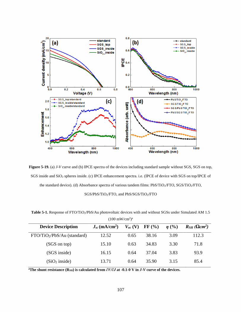
107
Figure 5-19. (a) J-V curve and (b) IPCE spectra of the devices including standard sample without SGS, SGS on top,
SGS inside and SiO2 spheres inside. (c) IPCE enhancement spectra. i.e. (IPCE of device with SGS on top/IPCE of
the standard device). (d) Absorbance spectra of various tandem films: PbS/TiO2/FTO, SGS/TiO2/FTO,
SGS/PbS/TiO2/FTO, and PbS/SGS/TiO2/FTO
Table 5-1. Response of FTO/TiO2/PbS/Au photovoltaic devices with and without SGSs under Simulated AM 1.5
(100 mW/cm2)a
Device Description Jsc (mA/cm2) Voc (V) FF (%) η (%) RSH (Ωcm2)
FTO/TiO2/PbS/Au (standard) 12.52 0.65 38.16 3.09 112.3
(SGS on top) 15.10 0.63 34.83 3.30 71.8
(SGS inside) 16.15 0.64 37.04 3.83 93.9
(SiO2 inside) 13.71 0.64 35.90 3.15 85.4
aThe shunt resistance (RSH) is calculated from ∂V/∂J at -0.1-0 V in J-V curve of the devices.

108
SGSs improve IPCE of the solar cells via multiple different mechanisms. First, an
increase in the photocurrent by SGS is due to plasmonic near-field coupling by LSPRs, which
decays concentrically from the outer surface of SGSs. A coupling of plasmon with incident light
generates a strong local electromagnetic field which stores the incident energy and facilitates
light absorption by the PbS films.65 Second, when SGSs are placed below PbS film, the
nanodomes are formed in the top Au electrode and produces an additional surface plasmonic
effect in visible region. Therefore, in SGS inside device, light intensity is locally increased from
the top and bottom surfaces of PbS film, leading to an even higher light absorption in near IR
regime. Third, the nanodome of Au electrode provides the second surface plasmon resonance.
This surface wave propagates along PbS-Au interface and gives more chance of light absorption
to the PbS film.195 These multiple effects of SGSs improve Jsc of SGS inside device at plasmonic
frequencies, which is manifested in IPCE spectra.
To further investigate the impact of the SGSs on the PbS-QD solar cells, we carried out
numerical simulation using a finite-difference time-domain (FDTD) method. In order to do the
simulation analysis of the plasmonic effect in PbS QD based solar cells, the geometric
parameters were approximated from electron microscopy pictures (Fig. 5-18), and the real
refractive index of the PbS QDs film was required and measured by a spectroscopic phase
modulated ellipsometer (Ellipsometer VUV-NIR, Horiba Jobin Yvon), since the optical
properties of the semiconductor materials are size dependent. The complex refractive index
contains real part and imaginary part and described as ṅ(λ) = n(λ) + ik(λ). The resulting n(λ) and
k(λ), captured from a ~ 150 nm thick PbS QDs film deposited on quartz substrate by dip coating,
are shown in Figure 5-20, in which the real values of the optical constants are much smaller than
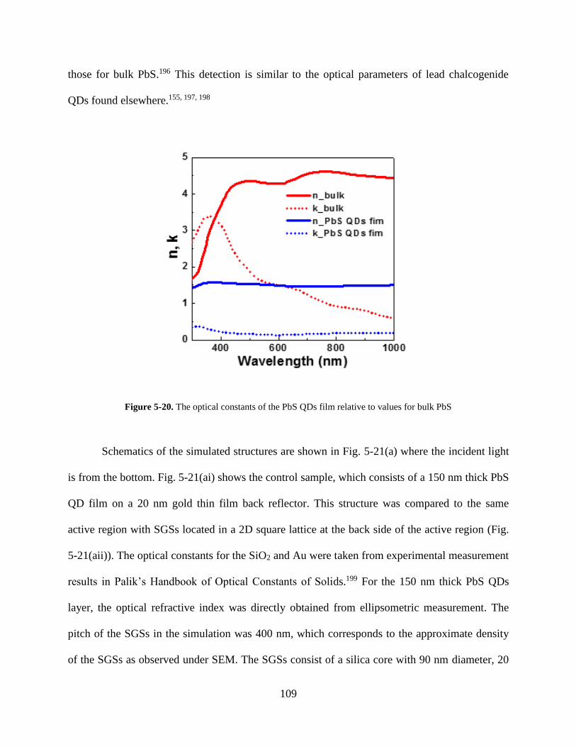
109
those for bulk PbS.196 This detection is similar to the optical parameters of lead chalcogenide
QDs found elsewhere.155, 197, 198
Figure 5-20. The optical constants of the PbS QDs film relative to values for bulk PbS
Schematics of the simulated structures are shown in Fig. 5-21(a) where the incident light
is from the bottom. Fig. 5-21(ai) shows the control sample, which consists of a 150 nm thick PbS
QD film on a 20 nm gold thin film back reflector. This structure was compared to the same
active region with SGSs located in a 2D square lattice at the back side of the active region (Fig.
5-21(aii)). The optical constants for the SiO2 and Au were taken from experimental measurement
results in Palik’s Handbook of Optical Constants of Solids.199 For the 150 nm thick PbS QDs
layer, the optical refractive index was directly obtained from ellipsometric measurement. The
pitch of the SGSs in the simulation was 400 nm, which corresponds to the approximate density
of the SGSs as observed under SEM. The SGSs consist of a silica core with 90 nm diameter, 20

110
nm gold intermediate layer, and 7 nm outer silica shell. The position dependent absorption per
unit volume is calculated from the divergence of the Poynting vector :
(5-4)
where εi(λ) is the imaginary part of the permittivity, ω = 2πc/λ is the photon angular
frequency, c is the speed of light, and E(r, λ) is the position and wavelength-dependent electric
field vector. The absorption spectra A(λ) is obtained by integrating over the PbS,
. This eliminates any parasitic absorption that may occur in the SGSs.
This eliminates any parasitic absorption that may occur in the SGSs. Results of the calculations
indicate that the addition of the plasmonic SGSs enhances the absorption for wavelengths larger
than 520 nm. Fig. 5-21(b) shows the local absorption per unit volume (in units of 1/nm3) for the
two structures shown in Fig. 5-21(a) at = 680 nm where a significant increase in IPCE by SGS
particles was experimentally observed (Fig. 5-19). The incident light is from the PbS QD layer
toward the Au layer and the electric vector of the incident light is parallel to x-axis in the
simulation. Dashed white lines indicate the location of the 150 nm thick PbS QD layer, the 20
nm thick Au reflector, as well as the outline of the SGSs. About 60% enhancement in absorption
occurs through the photoactive region at this wavelength ( = 680 nm) when the localized
surface plasmon is excited by the SGS. This clearly supports the experimental observation that
the SGS at the backside of the PbS film increased the IPCE by 50%.
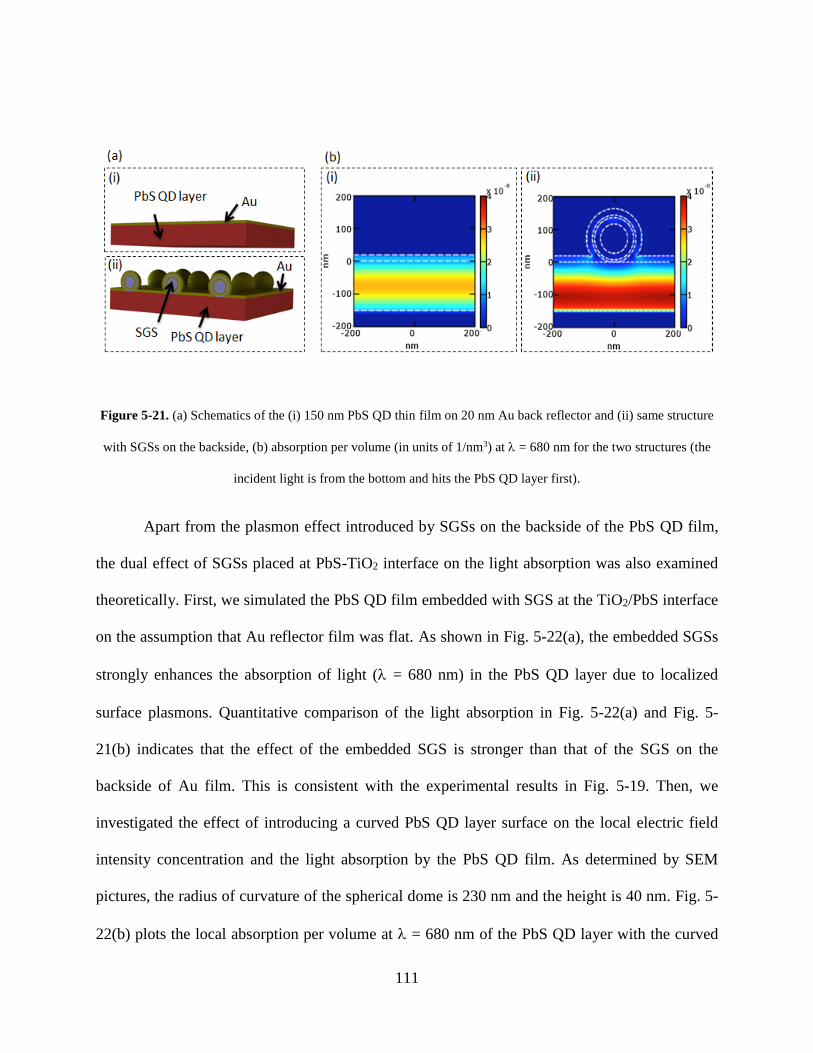
111
Figure 5-21. (a) Schematics of the (i) 150 nm PbS QD thin film on 20 nm Au back reflector and (ii) same structure
with SGSs on the backside, (b) absorption per volume (in units of 1/nm3) at = 680 nm for the two structures (the
incident light is from the bottom and hits the PbS QD layer first).
Apart from the plasmon effect introduced by SGSs on the backside of the PbS QD film,
the dual effect of SGSs placed at PbS-TiO2 interface on the light absorption was also examined
theoretically. First, we simulated the PbS QD film embedded with SGS at the TiO2/PbS interface
on the assumption that Au reflector film was flat. As shown in Fig. 5-22(a), the embedded SGSs
strongly enhances the absorption of light ( = 680 nm) in the PbS QD layer due to localized
surface plasmons. Quantitative comparison of the light absorption in Fig. 5-22(a) and Fig. 5-
21(b) indicates that the effect of the embedded SGS is stronger than that of the SGS on the
backside of Au film. This is consistent with the experimental results in Fig. 5-19. Then, we
investigated the effect of introducing a curved PbS QD layer surface on the local electric field
intensity concentration and the light absorption by the PbS QD film. As determined by SEM
pictures, the radius of curvature of the spherical dome is 230 nm and the height is 40 nm. Fig. 5-
22(b) plots the local absorption per volume at = 680 nm of the PbS QD layer with the curved

112
surface to illustrate the role of the nanodome separately. The result means that an additional
increase in the local electric field intensity by the uneven surface is introduced due to scattering
incident sunlight into the solar cell. These two effects may be combined to further enhance the
photoactive region absorption as shown in Fig. 5-22(c). A series of simulation results supports
the dual effect SGSs on the performance of PbS solar cells once the SGSs are placed between the
PbS film and the TiO2 film.
Figure 5-22. Absorption per volume at = 680 nm for (a) PbS QD thin film with embedded SGS, (b) PbS QD thin
film with the curved PbS surface, and (c) PbS QD thin film with SGS and the curved Au surface .
In order to illustrate the possible reason why, to some extent, the Voc and ff in the
plasmonic assisted device are suppressed, electron lifetime (τ) of the device was measured by the
open-circuit voltage decay (OCVD) technique, in which transient of Voc was measured as a
function of time using a 633 nm photodiode laser as the illumination source. Figure 5-23a shows
the τ in different devices, calculated from the decay curves of the Voc. When the SGSs are
submerged into the PbS film, the electron lifetime slightly decreased, indicating a higher charge
carrier recombination rate. This is due to the increased carrier diffusion length under the
113
protuberance of the PbS film and the decreased recombination resistance at the TiO2/PbS
interface. When the recombination rate is increase, Voc and ff are lowered. On the other hand, if
the SGSs are attached to the upper surface of the PbS film, the SGSs covered a part of the PbS
film beneath them and blocked the Au electrode penetration, leading to insufficient Schottky
contact. These result in small hollows which work as carrier recombination sites.
The electrochemical impedance spectroscopy (EIS) analysis was performed to study the
internal electrical parameters of the devices. For the FTO/TiO2/PbS/Au heterojunction device,
low frequency response ranging from ~kHz to mHz corresponds to the TiO2/PbS interface.160
Figure 5-23b shows the Nyquist plots of the devices with and without SGSs. In order to study the
impedance of the TiO2/PbS interface, complex impedance was measured from 0.1 Hz to 1 kHz in
illuminated condition under an external bias with a magnitude of open circuit voltage. The
results of the impedance measurement were fitted using a ZARC element which contains a
parallel resistance and a non-intuitive circuit element (CPE). The experimental data, plotted as
hollow dots, are simulated using multiple ZARC elements. The results of fitting for three cases
were presented in solid lines of Fig. 5-23b. Fitting results indicate that the recombination
resistance is 518 Ω for the control device, 486 Ω for the SGS top case, and 406 Ω for the SGS
bottom case. Lower recombination resistance means higher charge carrier recombination
probability. A difference in the recombination resistance results from the non-conformal coating
of PbS QDs. Since PbS films were deposited by a solution method, PbS QDs fill empty space
under the SGSs in the SGS inside case. However, when Au electrode was deposited on SGS
particles by E-beam evaporation technique (the SGS top case), Au did not conformally coat SGS
particles and photogenerated charges of PbS QDs were temporarily trapped in the empty space
and the carrier recombination rate was increased.
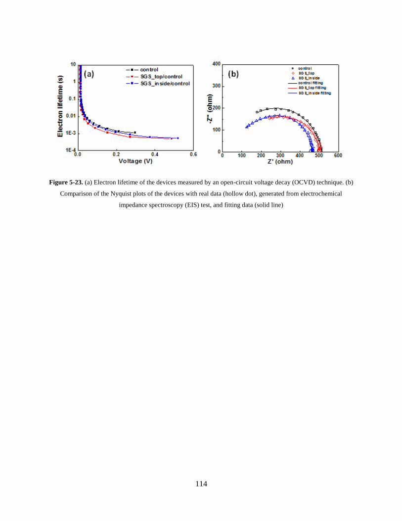
114
Figure 5-23. (a) Electron lifetime of the devices measured by an open-circuit voltage decay (OCVD) technique. (b)
Comparison of the Nyquist plots of the devices with real data (hollow dot), generated from electrochemical
impedance spectroscopy (EIS) test, and fitting data (solid line)
115
6.0 CONCLUSIONS AND FUTURE WORK
6.1 CONCLUSIONS
The research topics discussed in this dissertation cover the preparation of two kinds of plasmon
core-shell particles, Ag@SiO2 and SiO2@Au@SiO2, and their application in DSSCs and PbS
QDs based thin film heterojunction solar cells, respectively. In addition, plasmon tuning effect in
DSSCs has also been studied. Detail conclusions are summarized as following.
Core-shell particles coated with a uniform Ag layer were synthesized by a two-step
method. Light absorption and scattering in the visible range is significantly enhanced in
composite films containing the core-shell particles, leading to higher optical cross section of dyes
adsorbed on the mesoporous mixed films. The effect of the core-shell particles is theoretically
explained from the viewpoint of local field intensity and scattering efficiency. For 22 vol% core-
shell particles, the conversion rate of incident photons to electrons increases by more than 20%.
It is found that a balance among the near-field intensity, light scattering efficiency, and surface
area in the photoanodes determines the energy conversion efficiency of DSCs containing core-
shell particles.
Plasmon tuning effect was investigated in the DSSCs. It demonstrated that the observed
light harvesting enhancement is strongly size dependent. As the size of core increases, light
interacts with the surface plasmons of the core-shell particles in longer wavelength regime.

116
Tuning of the surface plasmons frequency is also found to benefit the energy conversion
efficiency of DSSCs with different sensitizing dyes. When the extinction spectrum of the
plasmonic particles is overlaid with the absorption spectrum of black dye with small optical cross
section, the short circuit current of DSSCs is almost doubled, with a negligible change in the
open circuit voltage. Our results provide a facile method to enhance light absorption of various
dyes with different light absorption spectra, via the surface plamsons.
Another plasmonic SGSs were prepared using the seeded metallization of silica spheres,
and successfully applied in the PbS based thin film heterojunction solar cell for light harvesting
enhancement. The SGSs can make up improved light absorption at visible and near IR regime,
600 nm ~ 700 nm and 800 nm ~ 1000 nm which PbS QDs (~ 1.67 eV) absorb photons weakly. It
proves from practical and theoretical studies that, either locating the SGSs on top of the PbS film
or inside of it, enhanced light absorption is attributed to the LSPRs of the SGSs. In addition, a
dual effect is realized by submerging the SGSs in the thin PbS film, since nanodome structures
are formed in the top Au anode. This self-made dual plasmon resonance can be further applied to
the other thin film photovoltaic devices for improved cell performance contribution.
6.2 FUTURE WORK
6.2.1 SGSs Application in DSSCs with Low Temperature UV Annealing
As mentioned above, the SGSs can enhance the light harvesting efficiency in the PbS QDs film
based solar cell. Initial trial also shows that the SGSs have the potential to increase the
conversion efficiency of the DSSCs, especially at longer wavelength region, since the plasmon

117
improved light absorption from Au nanoshell can cover a longer wavelength region comparing
with that from Ag nanoshell (Fig. 6-1a). However, initial trial shows that photoanode annealing
at high temperature will lose some light absorption enhancement at 600 nm ~ 900 nm (Fig. 6-
1b), revealing that the Au nanoshell is not stable at high temperature, so low temperature
annealing is necessary for the Au nanoshell case.
So far, low temperature photoanode annealing for DSSCs has attracted a great amount of
attention due to the potential application with the low cost flexible substrate, since the melting
point of the conductive polymer substrate, like polyethylene terephthalate (PET), is usually lower
than 250 oC. Thus, a modified UV annealing process combing a UV lamp (λ = 354 nm) with a
hot plate is demonstrated here. After annealing at 200 oC for 30 min under simultaneously UV
light exposure, the optical property of the composite film is retained.
Figure 6-1. (a) Absorbance spectra of the TiO2 and TiO2/SGSs_10 % composite films, as well as the theoretical
absorption coefficient spectrum of the SGSs. (b) Absorbance spectra of the composite film after different annealing
treatments. Inset shows the schematic setup of UV annealing
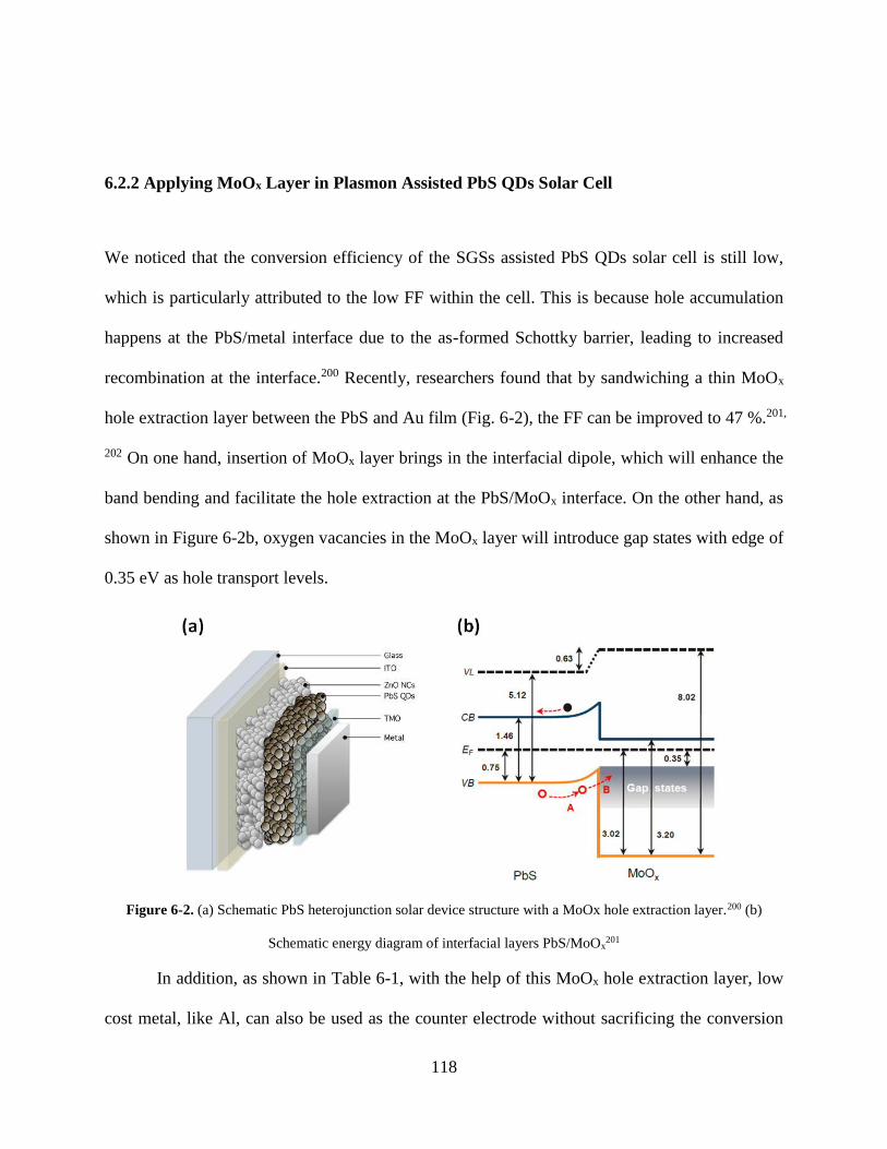
118
6.2.2 Applying MoOx Layer in Plasmon Assisted PbS QDs Solar Cell
We noticed that the conversion efficiency of the SGSs assisted PbS QDs solar cell is still low,
which is particularly attributed to the low FF within the cell. This is because hole accumulation
happens at the PbS/metal interface due to the as-formed Schottky barrier, leading to increased
recombination at the interface.200 Recently, researchers found that by sandwiching a thin MoOx
hole extraction layer between the PbS and Au film (Fig. 6-2), the FF can be improved to 47 %.201,
202 On one hand, insertion of MoOx layer brings in the interfacial dipole, which will enhance the
band bending and facilitate the hole extraction at the PbS/MoOx interface. On the other hand, as
shown in Figure 6-2b, oxygen vacancies in the MoOx layer will introduce gap states with edge of
0.35 eV as hole transport levels.
Figure 6-2. (a) Schematic PbS heterojunction solar device structure with a MoOx hole extraction layer.200 (b)
Schematic energy diagram of interfacial layers PbS/MoOx201
In addition, as shown in Table 6-1, with the help of this MoOx hole extraction layer, low
cost metal, like Al, can also be used as the counter electrode without sacrificing the conversion

119
efficiency of the solar cell. Thus, applying an extra MoOx layer in the SGSs assisted PbS QDs
solar cell will further enhance the total conversion efficiency of the device.
Table 6-1. PbS QD Solar Cell Operation Parameters for Devices with Various Anodes201
anode Voc (mV) Jsc (mA/cm2) FF (%) PCE (%)
10 nm MoOx/Al 524.5 17.9 48.7 4.46
20 nm MoOx/Al 549.5 17.9 41.5 4.20
10 nm MoOx/Ag 530.4 18.7 47.6 4.53
10 nm MoOx/Au 540.0 17.4 47.0 4.41
Al 83.8 5.6 26.0 0.12
Ag 212.1 11.4 30.2 0.73
Au 399.5 15.5 43 2.66
120
BIBLIOGRAPHY
1. Barnes, W. L.; Dereux, A.; Ebbesen, T. W. Nature 2003, 424, 824.
2. Wang, H.; Goodrich, G. P.; Tam, F.; Oubre, C.; Nordlander, P.; Halas, N. J. J. Phys.
Chem. B 2005, 109, 11083.
3. Maier, S. A.; Atwater, H. A. J. Appl. Phys. 2005, 98, 011101.
4. Ozbay, E. Science 2006, 311, 189.
5. Atwater, H. A. Sci. Am. 2007, 296, 56.
6. Wood, R. W. Phil. Mag. 1902, 4, 396.
7. Brongersma, M. L., Surface Plasmon Nanophotonics. Springer: New York, 2007.
8. Mie, G. Ann. Phys. 1908, 25, 377.
9. Ritchie, R. H. Phys. Rev. 1957, 106, 874.
10. Otto, A. Z Phys. 1968, 216, 398.
11. Kretschmann, E. R., H. Z. Naturf. 1968, A 23, 2135.
12. Stewart, M. E.; Anderton, C. R.; Thompson, L. B.; Maria, J.; Gray, S. K.; Rogers, J. A.;
Nuzzo, R. G. Chem. Rev. 2008, 108, 494.
13. Cunningh.Sl; Maradudi.Aa; Wallis, R. F. Phys. Rev. B 1974, 10, 3342.
14. Wark, A. W.; Lee, H. J.; Corn, R. M. Anal. Chem. 2005, 77, 3904.
15. Bohren, C. F.; Huffman, D. R., Absorption and Scattering of Light by Small Particles.
John Wiley and Sons: New York, 1983.
16. Willets, K. A.; Van Duyne, R. P. Ann. Rev. Phys. Chem. 2007, 58, 267.
121
17. Kreibig, U.; Vollmer, M. Optical Properties of Metal Clusters. Springer: New York,
1995.
18. Su, K. H.; Wei, Q. H.; Zhang, X.; Mock, J. J.; Smith, D. R.; Schultz, S. Nano Lett. 2003,
3, 1087.
19. Grand, J.; Adam, P. M.; Grimault, A. S.; Vial, A.; De la Chapelle, M. L.; Bijeon, J. L.;
Kostcheev, S.; Royer, P. Plasmonics 2006, 1, 135.
20. Prikulis, J.; Hanarp, P.; Olofsson, L.; Sutherland, D.; Kall, M. Nano Lett. 2004, 4, 1003.
21. Whitesides, G. M.; Love, J. C. Sci. Am. 2001, 285, 38.
22. Turkevitch, J. S., P. C.; Hillier, J. Discuss. Faraday Soc. 1951, 11.
23. Sun, Y. G.; Xia, Y. N. Science 2002, 298, 2176.
24. Sau, T. K.; Rogach, A. L. Adv. Mater. 2010, 22, 1781.
25. Murphy, C. J.; San, T. K.; Gole, A. M.; Orendorff, C. J.; Gao, J. X.; Gou, L.; Hunyadi, S.
E.; Li, T. J. Phys. Chem. B 2005, 109, 13857.
26. Perez-Juste, J.; Pastoriza-Santos, I.; Liz-Marzan, L. M.; Mulvaney, P. Coordin. Chem.
Rev. 2005, 249, 1870.
27. Xia, Y. N. X., Y. J.; Lim, B. K.; Skrabalak, S. E. Angew. Chem. Int. Ed. 2009, 48, 60.
28. Sau, T. K.; Rogach, A. L.; Jackel, F.; Klar, T. A.; Feldmann, J. Adv. Mater. 2010, 22,
1805.
29. Giannini, V.; Fernandez-Dominguez, A. I.; Sonnefraud, Y.; Roschuk, T.; Fernandez-
Garcia, R.; Maier, S. A. Small 2010, 6, 2498.
30. Oldenburg, S. J.; Averitt, R. D.; Westcott, S. L.; Halas, N. J. Chem. Phys. Lett. 1998, 288,
243.
31. Prodan, E.; Nordlander, P.; Halas, N. J. Nano Lett. 2003, 3, 1411.
32. Wang, H. B., D. W.; Nordlander, P.; Halas, N. J. Acc. Chem. Res. 2007, 40, 53.
33. Brinson, B. E.; Lassiter, J. B.; Levin, C. S.; Bardhan, R.; Mirin, N.; Halas, N. J. Langmuir
2008, 24, 14166.
34. Graf, C.; van Blaaderen, A. Langmuir 2002, 18, 524.

122
35. Loo, C.; Lin, A.; Hirsch, L.; Lee, M. H.; Barton, J.; Halas, N. J.; West, J.; Drezek, R.
Technol. Cancer Res. T. 2004, 3, 33.
36. Jain, P. K.; El-Sayed, M. A. Nano Lett. 2007, 7, 2854.
37. Halas, N. J.; Lal, S.; Chang, W. S.; Link, S.; Nordlander, P. Chem. Rev. 2011, 111, 3913.
38. Halas, N. J. Mrs Bull. 2005, 30, 362.
39. Prodan, E.; Radloff, C.; Halas, N. J.; Nordlander, P. Science 2003, 302, 419.
40. Oregan, B.; Gratzel, M. Nature 1991, 353, 737.
41. Frank, A. J.; Kopidakis, N.; van de Lagemaat, J. Coordin. Chem. Rev. 2004, 248, 1165.
42. Chen, C. Y.; Wang, M. K.; Li, J. Y.; Pootrakulchote, N.; Alibabaei, L.; Ngoc-le, C. H.;
Decoppet, J. D.; Tsai, J. H.; Gratzel, C.; Wu, C. G.; Zakeeruddin, S. M.; Gratzel, M. Acs
Nano 2009, 3, 3103.
43. Li, L.; Hao, Y.; Yang, X. C.; Zhao, J. Z.; Tian, H. N.; Teng, C.; Hagfeldt, A.; Sun, L. C.
Chemsuschem 2011, 4, 609.
44. Green, M. A.; Emery, K.; Hishikawa, Y.; Warta, W. Prog. Photovoltaics 2010, 18, 346.
45. Lee, J. K.; Yang, M. J. Mat. Sci. & Eng. B 2011, 176. 1142.
46. Robel, I.; Subramanian, V.; Kuno, M.; Kamat, P. V. J. Am. Chem. Soc. 2006, 128, 2385.
47. Tisdale, W. A.; Williams, K. J.; Timp, B. A.; Norris, D. J.; Aydil, E. S.; Zhu, X. Y.
Science 2010, 328, 1543.
48. Gratzel, M. Nature 2001, 414, 338.
49. Teng, C.; Yang, X. C.; Yuan, C. Z.; Li, C. Y.; Chen, R. K.; Tian, H. N.; Li, S. F.;
Hagfeldt, A.; Sun, L. C. Org. Lett. 2009, 11, 5542.
50. Sapp, S. A.; Elliott, C. M.; Contado, C.; Caramori, S.; Bignozzi, C. A. J. Am. Chem. Soc.
2002, 124, 11215.
51. Wang, M. K.; Chamberland, N.; Breau, L.; Moser, J. E.; Humphry-Baker, R.; Marsan, B.;
Zakeeruddin, S. M.; Gratzel, M. Nat. Chem. 2010, 2, 385.
52. Daeneke, T.; Kwon, T. H.; Holmes, A. B.; Duffy, N. W.; Bach, U.; Spiccia, L. Nat.
Chem. 2011, 3, 211.
53. Boschloo, G.; Hagfeldt, A. Acc. Chem. Res. 2009, 42, 1819.
123
54. Bai, Y.; Cao, Y. M.; Zhang, J.; Wang, M.; Li, R. Z.; Wang, P.; Zakeeruddin, S. M.;
Gratzel, M. Nat. Mater. 2008, 7, 626.
55. Cao, Y. M.; Zhang, J.; Bai, Y.; Li, R. Z.; Zakeeruddin, S. M.; Gratzel, M.; Wang, P. J.
Phys. Chem. C 2008, 112, 13775.
56. Bach, U.; Lupo, D.; Comte, P.; Moser, J. E.; Weissortel, F.; Salbeck, J.; Spreitzer, H.;
Gratzel, M. Nature 1998, 395, 583.
57. Ding, I. K.; Tetreault, N.; Brillet, J.; Hardin, B. E.; Smith, E. H.; Rosenthal, S. J.;
Sauvage, F.; Gratzel, M.; McGehee, M. D. Adv. Funct. Mater. 2009, 19, 2431.
58. Wang, P.; Zakeeruddin, S. M.; Comte, P.; Exnar, I.; Gratzel, M. J. Am. Chem. Soc. 2003,
125, 1166.
59. Stergiopoulos, T.; Arabatzis, I. M.; Katsaros, G.; Falaras, P. Nano Lett. 2002, 2, 1259.
60. Shah, A.; Torres, P.; Tscharner, R.; Wyrsch, N.; Keppner, H. Science 1999, 285, 692.
61. Krebs, F. C.; Tromholt, T.; Jorgensen, M. Nanoscale 2010, 2, 873.
62. Hoppe, H.; Sariciftci, N. S. J. Mater. Res. 2004, 19, 1924.
63. Deckman, H. W.; Roxlo, C. B.; Yablonovitch, E. Opt. Lett. 1983, 8, 491.
64. Polman, A. Science 2008, 322, 868.
65. Atwater, H. A.; Polman, A. Nat. Mater. 2010, 9, 205.
66. Hagglund, C.; Zach, M.; Petersson, G.; Kasemo, B. Appl. Phys. Lett. 2008, 92, 053110.
67. Westphalen, M.; Kreibig, U.; Rostalski, J.; Lüth, H.; Meissner, D. Sol. Energy Mater. Sol.
C 2000, 61, 97.
68. Slooff, L. H.; Veenstra, S. C.; Kroon, J. M.; Moet, D. J. D.; Sweelssen, J.; Koetse, M. M.
Appl. Phys. Lett. 2007, 90, 143506.
69. Moskovits, M. Rev. Mod. Phys. 1985, 57, 783.
70. Souza, G. R.; Levin, C. S.; Hajitou, A.; Pasqualini, R.; Arap, W.; Miller, J. H. Anal.
Chem. 2006, 78, 6232.
71. Jiang, J.; Bosnick, K.; Maillard, M.; Brus, L. J. Phys. Chem. B 2003, 107, 9964.
124
72. Jackson, J. B.; Westcott, S. L.; Hirsch, L. R.; West, J. L.; Halas, N. J. Appl. Phys. Lett.
2003, 82, 257.
73. Jackson, J. B.; Halas, N. J. P. Natl. Acad. Sci. 2004, 101, 17930.
74. Kim, K.; Huang, S. W.; Ashkenazi, S.; O'Donnell, M.; Agarwal, A.; Kotov, N. A.;
Denny, M. F.; Kaplan, M. J. Appl. Phys. Lett. 2007, 90, 223901.
75. Chen, Y. S.; Frey, W.; Kim, S.; Kruizinga, P.; Homan, K.; Emelianov, S. Nano Lett.
2011, 11, 348.
76. Kim, J. W.; Galanzha, E. I.; Shashkov, E. V.; Moon, H. M.; Zharov, V. P. Nat.
Nanotechnol. 2009, 4, 688.
77. Oraevsky, A. A.; Karabutov, A. A.; Savateeva, E. V. Proc. SPIE 2001, 4434.
78. Agarwal, A.; Huang, S. W.; O'Donnell, M.; Day, K. C.; Day, M.; Kotov, N.; Ashkenazi,
S. J. Appl. Phys. 2007, 102, 064701.
79. Skrabalak, S. E.; Chen, J. Y.; Sun, Y. G.; Lu, X. M.; Au, L.; Cobley, C. M.; Xia, Y. N.
Acc. Chem. Res. 2008, 41, 1587.
80. Kim, K.; Kim, H. S.; Park, H. K. Langmuir 2006, 22, 8083.
81. Pol, V. G.; Srivastava, D. N.; Palchik, O.; Palchik, V.; Slifkin, M. A.; Weiss, A. M.;
Gedanken, A. Langmuir 2002, 18, 3352.
82. Jiang, Z. J.; Liu, C. Y. J. Phys. Chem. B 2003, 107, 12411.
83. Kobayashi, Y.; Salgueirino-Maceira, V.; Liz-Marzan, L. M. Chem. Mater. 2001, 13,
1630.
84. Deng, Z. W.; Chen, M.; Wu, L. M. J. Phys. Chem. C 2007, 111, 11692.
85. Brown, M. D.; Suteewong, T.; Kumar, R. S. S.; D'Innocenzo, V.; Petrozza, A.; Lee, M.
M.; Wiesner, U.; Snaith, H. J. Nano Lett. 2011, 11, 438.
86. Qi, J. F.; Dang, X. N.; Hammond, P. T.; Belcher, A. M. Acs Nano 2011, 5, 7108.
87. Novotny, L.; Hecht, B.; Pohl, D. W. J. Appl. Phys. 1997, 81, 1798.
88. Prodan, E.; Nordlander, P.; Halas, N. J. Chem. Phys. Lett. 2003, 368, 94.
89. Weeber, J. C.; Dereux, A.; Girard, C.; Krenn, J. R.; Goudonnet, J. P. Phys. Rev. B 1999,
60, 9061.
125
90. Purcell, E. M.; Pennypac, Cr. Astrophys. J. 1973, 186, 705.
91. Draine, B. T.; Flatau, P. J. J. Opt. Soc. Am. A 1994, 11, 1491.
92. Jain, P. K.; Lee, K. S.; El-Sayed, I. H.; El-Sayed, M. A. J. Phys. Chem. B 2006, 110,
7238.
93. Taflove, A. Computational Electrodynamics. Artech House: Boston, 1995.
94. Vial, A.; Laroche, T. J. Phys. D Appl. Phys. 2007, 40, 7152.
95. Stratton, J. A., Electromagnetic Theory. McGraw-Hill: New York, 1941.
96. Smith, D. D.; Fuller, K. A. J. Opt. Soc. Am. B 2002, 19, 2449.
97. Hamann, T. W.; Jensen, R. A.; Martinson, A. B. F.; Van Ryswyk, H.; Hupp, J. T. Energ.
Environ. Sci. 2008, 1, 66.
98. Argazzi, R.; Iha, N. Y. M.; Zabri, H.; Odobel, F.; Bignozzi, C. A. Coordin. Chem. Rev.
2004, 248, 1299.
99. Raether, H., Surface Plasmons on Smooth and Rough Surfaces and on Gratings.
Springer-Verlag: Berlin, New York, 1988.
100. Hallermann, F.; Rockstuhl, C.; Fahr, S.; Seifert, G.; Wackerow, S.; Graener, H.; Plessen,
G. V.; Lederer, F. Phys. Stat. Sol. (a) 2008, 205, 2844.
101. Nakayama, K.; Tanabe, K.; Atwater, H. A. Appl. Phys. Lett. 2008, 93, 121904.
102. Morfa, A. J.; Rowlen, K. L.; Reilly, T. H.; Romero, M. J.; Van de Lagemaat, J. Appl.
Phys. Lett. 2008, 92, 013504.
103. Kim, S. S.; Na, S. I.; Jo, J.; Kim, D. Y.; Nah, Y. C. Appl. Phys. Lett. 2008, 93, 073307.
104. Standridge, S. D.; Schatz, G. C.; Hupp, J. T. J. Am. Chem. Soc. 2009, 131, 8407.
105. Chou, C. S.; Yang, R. Y.; Yeh, C. K.; Lin, Y. J. Powder Technol. 2009, 194, 95.
106. Wen, C. I., K.; Kishima, M.; Yamada, K. Sol. Energ. Mat. Sol. Cells 2000, 61, 339.
107. Zaban, A.; Greenshtein, M.; Bisquert, J. Chemphyschem 2003, 4, 859.
108. Bisquert, J.; Zaban, A.; Greenshtein, M.; Mora-Sero, I. J. Am. Chem. Soc. 2004, 126,
13550.
109. Nakade, S.; Kanzaki, T.; Wada, Y.; Yanagida, S. Langmuir 2005, 21, 10803.

126
110. Nakade, S.; Kanzaki, T.; Kambe, S.; Wada, Y. J.; Yanagida, S. Langmuir 2005, 21,
11414.
111. Wang, Q.; Moser, J. E.; Gratzel, M. J. Phys. Chem. B 2005, 109, 14945.
112. Kalyanasundaram, K. Dye-sensitized solar cells. EPFL Press: 2010.
113. Ding, B.; Lee, B. J.; Yang, M. J.; Jung, H. S.; Lee, J. K. Adv. Energy Mater. 2011, 1, 415.
114. Stober, W.; Fink, A.; Bohn, E. J. Colloid Interf. Sci. 1968, 26, 62.
115. Zaban, A.; Ferrere, S.; Sprague, J.; Gregg, B. A. J. Phys. Chem. B 1997, 101, 55.
116. Park, N. G.; Kim, K. M.; Kang, M. G.; Ryu, K. S.; Chang, S. H.; Shin, Y. J. Adv. Mater.
2005, 17, 2349.
117. Preston, T. C.; Signorell, R. Acs Nano 2009, 3, 3696.
118. Wei, H.; Reyes-Coronado, A.; Nordlander, P.; Aizpurua, J.; Xu, H. X. Acs Nano 2010, 4,
2649.
119. Zuloaga, J.; Prodan, E.; Nordlander, P. Acs Nano 2010, 4, 5269.
120. Lal, S.; Link, S.; Halas, N. J. Nat. Photonics 2007, 1, 641.
121. Le, F.; Brandl, D. W.; Urzhumov, Y. A.; Wang, H.; Kundu, J.; Halas, N. J.; Aizpurua, J.;
Nordlander, P. Acs Nano 2008, 2, 707.
122. Love, S. A.; Marquis, B. J.; Haynes, C. L. Appl. Spectrosc. 2008, 62, 346a.
123. Loo, C.; Lowery, A.; Halas, N. J.; West, J.; Drezek, R. Nano Lett. 2005, 5, 709.
124. Hirsch, L. R.; Stafford, R. J.; Bankson, J. A.; Sershen, S. R.; Rivera, B.; Price, R. E.;
Hazle, J. D.; Halas, N. J.; West, J. L. P. Natl. Acad. Sci. 2003, 100, 13549.
125. Sershen, S. R.; Westcott, S. L.; Halas, N. J.; West, J. L. J. Biomed. Mater. Res. 2000, 51,
293.
126. Huang, C. Y.; Hsu, Y. C.; Chen, J. G.; Suryanarayanan, V.; Lee, K. M.; Ho, K. C. Sol.
Energ. Mat. Sol. C 2006, 90, 2391.
127. Kang, M. G.; Ryu, K. S.; Chang, S. H.; Park, N. G.; Hong, J. S.; Kim, K. J. B Kor. Chem.
Soc. 2004, 25, 742.
128. Chou, C. S.; Yang, R. Y.; Yeh, C. K.; Lin, Y. J. Powder. Technol. 2009, 194, 95.

127
129. Gratzel, M. Prog. Photovoltaics 2000, 8, 171.
130. Hara, K.; Nishikawa, T.; Kurashige, M.; Kawauchi, H.; Kashima, T.; Sayama, K.; Alka,
K.; Arakawa, H. Sol. Energ. Mat. Sol. C 2005, 85, 21.
131. Altobello, S.; Argazzi, R.; Caramori, S.; Contado, C.; Da Fre, S.; Rubino, P.; Chone, C.;
Larramona, G.; Bignozzi, C. A. J. Am. Chem. Soc. 2005, 127, 15342.
132. Wang, Z. S.; Cui, Y.; Dan-Oh, Y.; Kasada, C.; Shinpo, A.; Hara, K. J. Phys. Chem. C
2007, 111, 7224.
133. Chang, S.; Li, Q.; Xiao, X. D.; Wong, K. Y.; Chen, T. Energ. Environ. Sci. 2012, 5,
9444.
134. Averitt, R. D.; Sarkar, D.; Halas, N. J. Phys. Rev. Lett. 1997, 78, 4217.
135. Wang, Z. S.; Kawauchi, H.; Kashima, T.; Arakawa, H. Coordin. Chem. Rev. 2004, 248,
1381.
136. Ding, B.; Yang, M. J.; Lee, B. J.; Lee, J. K. RSC Advances 2013, 3, 9690.
137. Nazeeruddin, M. K.; Kay, A.; Rodicio, I.; Humphrybaker, R.; Muller, E.; Liska, P.;
Vlachopoulos, N.; Gratzel, M. J. Am. Chem. Soc. 1993, 115, 6382.
138. Nazeeruddin, M. K.; Pechy, P.; Renouard, T.; Zakeeruddin, S. M.; Humphry-Baker, R.;
Comte, P.; Liska, P.; Cevey, L.; Costa, E.; Shklover, V.; Spiccia, L.; Deacon, G. B.;
Bignozzi, C. A.; Gratzel, M. J. Am. Chem. Soc. 2001, 123, 1613.
139. Lee, S.; Cho, I. S.; Lee, J. H.; Kim, D. H.; Kim, D. W.; Kim, J. Y.; Shin, H.; Lee, J. K.;
Jung, H. S.; Park, N. G.; Kim, K.; Ko, M. J.; Hong, K. S. Chem. Mater. 2010, 22, 1958.
140. Huang, F. Z.; Chen, D. H.; Zhang, X. L.; Caruso, R. A.; Cheng, Y. B. Adv. Funct. Mater.
2010, 20, 1301.
141. Lee, J. K.; Jeong, B. H.; Jang, S. I.; Yeo, Y. S.; Park, S. H.; Kim, J. U.; Kim, Y. G.; Jang,
Y. W.; Kim, M. R. J. Mater. Sci.-Mater. El. 2009, 20, 446.
142. Talapin, D. V.; Lee, J. S.; Kovalenko, M. V.; Shevchenko, E. V. Chem. Rev. 2010, 110,
389.
143. Tang, J. A.; Sargent, E. H. Adv. Mater. 2011, 23, 12.
144. Hines, M. A.; Scholes, G. D. Adv. Mater. 2003, 15, 1844.
145. McDonald, S. A.; Konstantatos, G.; Zhang, S. G.; Cyr, P. W.; Klem, E. J. D.; Levina, L.;
Sargent, E. H. Nat. Mater. 2005, 4, 138.

128
146. Nozik, A. J. Annu. Rev. Phys. Chem. 2001, 52, 193.
147. Nozik, A. J. Physica E 2002, 14, 115.
148. Ellingson, R. J.; Beard, M. C.; Johnson, J. C.; Yu, P. R.; Micic, O. I.; Nozik, A. J.;
Shabaev, A.; Efros, A. L. Nano Lett. 2005, 5, 865.
149. Sukhovatkin, V.; Hinds, S.; Brzozowski, L.; Sargent, E. H. Science 2009, 324, 1542.
150. Sambur, J. B.; Novet, T.; Parkinson, B. A. Science 2010, 330, 63.
151. Semonin, O. E.; Luther, J. M.; Choi, S.; Chen, H. Y.; Gao, J. B.; Nozik, A. J.; Beard, M.
C. Science 2011, 334, 1530.
152. Sargent, E. H. Adv. Mater. 2008, 20, 3958.
153. Klem, E. J. D.; MacNeil, D. D.; Levina, L.; Sargent, E. H. Adv. Mater. 2008, 20, 3433.
154. Koleilat, G. I.; Levina, L.; Shukla, H.; Myrskog, S. H.; Hinds, S.; Pattantyus-Abraham,
A. G.; Sargent, E. H. Acs Nano 2008, 2, 833.
155. Law, M.; Beard, M. C.; Choi, S.; Luther, J. M.; Hanna, M. C.; Nozik, A. J. Nano Lett.
2008, 8, 3904.
156. Luther, J. M.; Law, M.; Beard, M. C.; Song, Q.; Reese, M. O.; Ellingson, R. J.; Nozik, A.
J. Nano Lett. 2008, 8, 3488.
157. Law, M.; Luther, J. M.; Song, O.; Hughes, B. K.; Perkins, C. L.; Nozik, A. J. J. Am.
Chem. Soc. 2008, 130, 5974.
158. Luther, J. M.; Law, M.; Song, Q.; Perkins, C. L.; Beard, M. C.; Nozik, A. J. Acs Nano
2008, 2, 271.
159. Pattantyus-Abraham, A. G.; Kramer, I. J.; Barkhouse, A. R.; Wang, X. H.; Konstantatos,
G.; Debnath, R.; Levina, L.; Raabe, I.; Nazeeruddin, M. K.; Gratzel, M. Sargent. E. H.
ACS Nano 2010, 4, 3374.
160. Etgar, L.; Moehl, T.; Gabriel, S.; Hickey, S. G.; Eychmuller, A.; Gratzel, M. Acs Nano
2012, 6, 3092.
161. Luther, J. M.; Gao, J. B.; Lloyd, M. T.; Semonin, O. E.; Beard, M. C.; Nozik, A. J. Adv.
Mater. 2010, 22, 3704.
162. Barkhouse, D. A. R.; Pattantyus-Abraham, A. G.; Levina, L.; Sargent, E. H. Acs Nano
2008, 2, 2356.

129
163. Johnston, K. W.; Pattantyus-Abraham, A. G.; Clifford, J. P.; Myrskog, S. H.; Hoogland,
S.; Shukla, H.; Klem, J. D.; Levina, L.; Sargent, E. H. Appl. Phys. Lett. 2008, 92, 122111.
164. Gao, J. B.; Luther, J. M.; Semonin, O. E.; Ellingson, R. J.; Nozik, A. J.; Beard, M. C.
Nano Lett. 2011, 11, 1002.
165. Szendrei, K.; Gomulya, W.; Yarema, M.; Heiss, W.; Loi, M. A. Appl. Phys. Lett. 2010,
97, 061103.
166. Klem, E. J. D.; Shukla, H.; Hinds, S.; MacNeil, D. D.; Levina, L.; Sargent, E. H. Appl.
Phys. Lett. 2008, 92, 151115.
167. Turyanska, L.; Elfurawi, U.; Li, M.; Fay, M. W.; Thomas, N. R.; Mann, S.; Blokland, J.
H.; Christianen, P. C. M.; Patane, A. Nanotechnology 2009, 20, 315604.
168. Baik, S. J.; Kim, K.; Lim, K. S.; Jung, S.; Park, Y. C.; Han, D. G.; Lim, S.; Yoo, S.;
Jeong, S. J. Phys. Chem. C 2011, 115, 607.
169. Zhao, N.; Osedach, T. P.; Chang, L. Y.; Geyer, S. M.; Wanger, D.; Binda, M. T.; Arango,
A. C.; Bawendi, M. G.; Bulovic, V. Acs Nano 2010, 4, 3743.
170. Gao, J. B.; Jeong, S.; Lin, F.; Erslev, P. T.; Semonin, O. E.; Luther, J. M.; Beard, M. C.
Appl. Phys. Lett. 2013, 102, 043506.
171. Ferry, V. E.; Verschuuren, M. A.; Li, H. B. T.; Verhagen, E.; Walters, R. J.; Schropp, R.
E. I.; Atwater, H. A.; Polman, A. Opt. Express 2010, 18, A237.
172. Spinelli, P.; Ferry, V. E.; van de Groep, J.; van Lare, M.; Verschuuren, M. A.; Schropp,
R. E. I.; Atwater, H. A.; Polman, A. J. Optics 2012, 14, 24002.
173. Deceglie, M. G.; Ferry, V. E.; Alivisatos, A. P.; Atwater, H. A. Nano Lett. 2012, 12,
2894.
174. Ding, I. K.; Zhu, J.; Cai, W. S.; Moon, S. J.; Cai, N.; Wang, P.; Zakeeruddin, S. M.;
Gratzel, M.; Brongersma, M. L.; Cui, Y.; McGehee, M. D. Adv. Energy Mater. 2011, 1,
52.
175. Li, X. H.; Choy, W. C. H.; Huo, L. J.; Xie, F. X.; Sha, W. E. I.; Ding, B. F.; Guo, X.; Li,
Y. F.; Hou, J. H.; You, J. B.; Yang, Y. Adv. Mater. 2012, 24, 3046.
176. Wang, D. H.; Kim, D. Y.; Choi, K. W.; Seo, J. H.; Im, S. H.; Park, J. H.; Park, O. O.;
Heeger, A. J. Angew. Chem. Int. Edit 2011, 50, 5519.
177. Kulkarni, A. P.; Noone, K. M.; Munechika, K.; Guyer, S. R.; Ginger, D. S. Nano Lett.
2010, 10, (4), 1501-1505.
130
178. Schwartzberg, A. M.; Olson, T. Y.; Talley, C. E.; Zhang, J. Z. J. Phys. Chem. B 2006,
110, 19935.
179. Chen, J. Y.; McLellan, J. M.; Siekkinen, A.; Xiong, Y. J.; Li, Z. Y.; Xia, Y. N. J. Am.
Chem. Soc. 2006, 128, 14776.
180. Skrabalak, S. E.; Chen, J. Y.; Sun, Y. G.; Lu, X. M.; Au, L.; Cobley, C. M.; Xia, Y. N.
Accounts Chem. Res. 2008, 41, 1587.
181. Wang, H.; Wu, Y. P.; Lassiter, B.; Nehl, C. L.; Hafner, J. H.; Nordlander, P.; Halas, N. J.
P. Natl. Acad. Sci. 2006, 103, 10856.
182. Lassiter, J. B.; Knight, M. W.; Mirin, N. A.; Halas, N. J. Nano Lett. 2009, 9, 4326.
183. Lu, Y.; Liu, G. L.; Kim, J.; Mejia, Y. X.; Lee, L. P. Nano Lett. 2005, 5, 119.
184. Sau, T. K.; Murphy, C. J. Langmuir 2004, 20, 6414.
185. Dreaden, E. C.; Alkilany, A. M.; Huang, X. H.; Murphy, C. J.; El-Sayed, M. A. Chem.
Soc. Rev. 2012, 41, 2740.
186. Huang, X. H.; El-Sayed, I. H.; Qian, W.; El-Sayed, M. A. J. Am. Chem. Soc. 2006, 128,
2115.
187. Dang, X. N.; Qi, J. F.; Klug, M. T.; Chen, P. Y.; Yun, D. S.; Fang, N. X.; Hammond, P.
T.; Belcher, A. M. Nano Lett. 2013, 13, 637.
188. Paz-Soldan, D.; Lee, A.; Thon, S. M.; Adachi, M. M.; Dong, H.; Maraghechi, P.; Yuan,
M.; Labelle, A. J.; Hoogland, S.; Liu, K.; Kumacheva, E.; Sargent, E. H. Nano Lett. 2013,
13, 1502.
189. Tang, J.; Kemp, K. W.; Hoogland, S.; Jeong, K. S.; Liu, H.; Levina, L.; Furukawa, M.;
Wang, X. H.; Debnath, R.; Cha, D. K.; Chou, K. W.; Fischer, A.; Amassian, A.; Asbury,
J. B.; Sargent, E. H. Nat. Mater. 2011, 10, 765.
190. Watts, J. F.; Wolstenholme, J.; Wiley, J. An introduction to surface analysis by XPS and
AES. Wiley Online Library: 2003.
191. Graf, C.; Vossen, D. L. J.; Imhof, A.; Van Blaaderen, A. Langmuir 2003, 19, 6693.
192. Duff, D. G.; Baiker, A.; Edwards, P. P. Langmuir 1993, 9, 2301.
193. Wang, H.; Brandl, D. W.; Le, F.; Nordlander, P.; Halas, N. J. Nano Lett. 2006, 6, 827.
194. Li, J. F.; Huang, Y. F.; Ding, Y.; Yang, Z. L.; Li, S. B.; Zhou, X. S.; Fan, F. R.; Zhang,
W.; Zhou, Z. Y.; Wu, D. Y.; Ren, B.; Wang, Z. L.; Tian, Z. Q. Nature 2010, 464, 392.
131
195. Ferry, V. E.; Sweatlock, L. A.; Pacifici, D.; Atwater, H. A. Nano Lett. 2008, 8, 4391.
196. Kanazawa, H.; Adachi, S. J. Appl. Phys. 1998, 83, 5997.
197. Paquet, C.; Yoshino, F.; Levina, L.; Gourevich, I.; Sargent, E. H.; Kumacheva, E. Adv.
Funct. Mater. 2006, 16, 1892.
198. Ehrler, B.; Wilson, M. W. B.; Rao, A.; Friend, R. H.; Greenham, N. C. Nano Lett. 2012,
12, 1053.
199. Palik, E. D., Handbook of Optical Constants of Solids. Academic Press: 1997.
200. Gao, J. B.; Jeong, S. H.; Semonin, O. E.; Ellingso, R. J.; Nozik, A. J.; Beard, M. C.,
Annealing Effect of PbS Quantum Dot Solar Cells. In Photovoltaic Specialists
Conference (PVSC), 2011 37th IEEE, Seattle, WA, 2011; pp 002619.
201. Gao, J. B.; Perkins, C. L.; Luther, J. M.; Hanna, M. C.; Chen, H. Y.; Semonin, O. E.;
Nozik, A. J.; Ellingson, R. J.; Beard, M. C. Nano Lett. 2011, 11, 3263.
202. Jean, J.; Chang, S.; Brown, P. R.; Cheng, J. J.; Rekemeyer, P. H.; Bawendi, M. C.;
Gradecak, S.; Bulovic, V. Adv. Mater. 2013, 25, 2790.
Related Documents


![Enhancing the Angular Sensitivity of Plasmonic Sensors ...biotheory.phys.cwru.edu/PDF/AOM.pdf · ultrasensitive plasmonic biosensors.[29,30] A plasmonic nanorod metamaterial (Type](https://static.cupdf.com/doc/110x72/5fcdd2c6db367d06a677e7be/enhancing-the-angular-sensitivity-of-plasmonic-sensors-ultrasensitive-plasmonic.jpg)


