Surface plasmon sensor with enhanced sensitivity using top nano dielectric layer Amit Lahav, a Atef Shalabaney, b and Ibrahim Abdulhalim c Department of Electro-optic Engineering Ben Gurion University, Beer Sheva 84105, Israel a [email protected] , b [email protected] , c [email protected] Abstract. Increasing the sensitivity of surface plasmon resonance (SPR) sensors is important to enable controlling small concentrations of materials in liquid solutions or for gas sensing. Upon using a 10-15 nm top layer of dielectric film with a high value of the real part ′ ε of the dielectric function, on top of an SPR sensor in the Kretschmann configuration, the sensitivity is improved by few times. The imaginary part ′′ ε of the top nano layer permittivity needs to be small enough in order to reduce the losses and get sharper dips. The stability of the sensor is also improved because the nano layer is protecting the silver from interacting with the environment. In the near infrared range, the sensitivity is enhanced contrary to the standard SPR mode without top nanolayer. The calculated evanescent field is enhanced near the top layer – analyte interface, thus the enhancement is partially due to this fact and partially due to an increase of the interaction length as a waveguiding effect. Keywords: SPR and GWSPR sensors, evanescent field, field enhancement, sensitivity. 1 INTRODUCTION Optical sensors have improved significantly both due to the discovery of new enhancement physical phenomena [1] and due to the developed electronic, computing, signal processing and other mature technologies when integrated into a system [2]. Surface plasmon resonance (SPR) sensors are widely recognized as valuable tools for investigating surface interactions and sensing of gases and biomaterials [3]. A surface plasmon is a longitudinal charge density wave propagating along the metal dielectric interface [4-6]. The guided wave SPR (GWSPR) configuration is similar to the SPR with an addition of a thin film between the metal layer and the cover material (the analyte to be sensed) thick enough to support guided modes. In the last two decades few methods were proposed to improve the sensitivity of the SPR sensor using the long range SPR method [7-8], combinations of metals [9-12], addition of gratings on top of the metal [13-14] and interferometric methods based on phase measurement [15-19], although recent study [20] showed that the enhanced sensitivity reported by phase measurement techniques is questionable because its accuracy is still limited by the accuracy of intensity measurement. In this work we present a method to improve the sensitivity and stability of the SPR in the Kretschmann configuration by adding a top nanolayer on the metal film using standard materials. The GWSPR mode is possible by introducing a dielectric layer between the metal and the dielectric cover thick enough to support guided optical waves so that an asymmetric metal clad waveguide is produced in which TE and TM modes can exist as shown in Fig. 1. These modes are propagating along the film and can also be used for sensing of the cover dielectric medium due to the evanescent field. In our case the top layer is thinner than the cutoff required for the TM modes to be guided and therefore we call it the near GWSPR (NGWSPR). The introduction of thin ZrO 2 layer on top of the silver film was done by Gent et al. [21] for the purpose of protection and they observed Journal of Nanophotonics, Vol. 3, 031501 (21 January 2009) © 2009 Society of Photo-Optical Instrumentation Engineers [DOI: 10.1117/1.3079803] Received 19 Dec 2008; accepted 14 Jan 2009; published 21 Jan 2009 [CCC: 19342608/2009/$25.00] Journal of Nanophotonics, Vol. 3, 031501 (2009) Page 1

Welcome message from author
This document is posted to help you gain knowledge. Please leave a comment to let me know what you think about it! Share it to your friends and learn new things together.
Transcript
Surface plasmon sensor with enhanced sensitivity using top nano dielectric layer
Amit Lahav,a Atef Shalabaney, b and Ibrahim Abdulhalimc
Department of Electro-optic Engineering Ben Gurion University, Beer Sheva 84105, Israel
[email protected], [email protected], [email protected]
Abstract. Increasing the sensitivity of surface plasmon resonance (SPR) sensors is important to enable controlling small concentrations of materials in liquid solutions or for gas sensing. Upon using a 10-15 nm top layer of dielectric film with a high value of the real part ′ε of the dielectric function, on top of an SPR sensor in the Kretschmann configuration, the sensitivity is improved by few times. The imaginary part ′′ε of the top nano layer permittivity needs to be small enough in order to reduce the losses and get sharper dips. The stability of the sensor is also improved because the nano layer is protecting the silver from interacting with the environment. In the near infrared range, the sensitivity is enhanced contrary to the standard SPR mode without top nanolayer. The calculated evanescent field is enhanced near the top layer – analyte interface, thus the enhancement is partially due to this fact and partially due to an increase of the interaction length as a waveguiding effect.
Keywords: SPR and GWSPR sensors, evanescent field, field enhancement, sensitivity.
1 INTRODUCTION Optical sensors have improved significantly both due to the discovery of new enhancement physical phenomena [1] and due to the developed electronic, computing, signal processing and other mature technologies when integrated into a system [2]. Surface plasmon resonance (SPR) sensors are widely recognized as valuable tools for investigating surface interactions and sensing of gases and biomaterials [3]. A surface plasmon is a longitudinal charge density wave propagating along the metal dielectric interface [4-6]. The guided wave SPR (GWSPR) configuration is similar to the SPR with an addition of a thin film between the metal layer and the cover material (the analyte to be sensed) thick enough to support guided modes. In the last two decades few methods were proposed to improve the sensitivity of the SPR sensor using the long range SPR method [7-8], combinations of metals [9-12], addition of gratings on top of the metal [13-14] and interferometric methods based on phase measurement [15-19], although recent study [20] showed that the enhanced sensitivity reported by phase measurement techniques is questionable because its accuracy is still limited by the accuracy of intensity measurement.
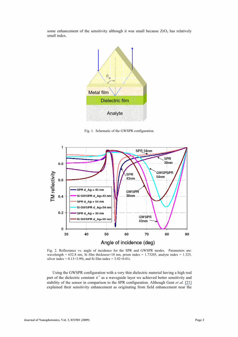
In this work we present a method to improve the sensitivity and stability of the SPR in the Kretschmann configuration by adding a top nanolayer on the metal film using standard materials. The GWSPR mode is possible by introducing a dielectric layer between the metal and the dielectric cover thick enough to support guided optical waves so that an asymmetric metal clad waveguide is produced in which TE and TM modes can exist as shown in Fig. 1. These modes are propagating along the film and can also be used for sensing of the cover dielectric medium due to the evanescent field. In our case the top layer is thinner than the cutoff required for the TM modes to be guided and therefore we call it the near GWSPR (NGWSPR). The introduction of thin ZrO2 layer on top of the silver film was done by Gent et al. [21] for the purpose of protection and they observed
Journal of Nanophotonics, Vol. 3, 031501 (21 January 2009)
© 2009 Society of Photo-Optical Instrumentation Engineers [DOI: 10.1117/1.3079803]Received 19 Dec 2008; accepted 14 Jan 2009; published 21 Jan 2009 [CCC: 19342608/2009/$25.00]Journal of Nanophotonics, Vol. 3, 031501 (2009) Page 1
some enhancement of the sensitivity although it was small because ZrO2 has relatively small index.
Fig. 1. Schematic of the GWSPR configuration.
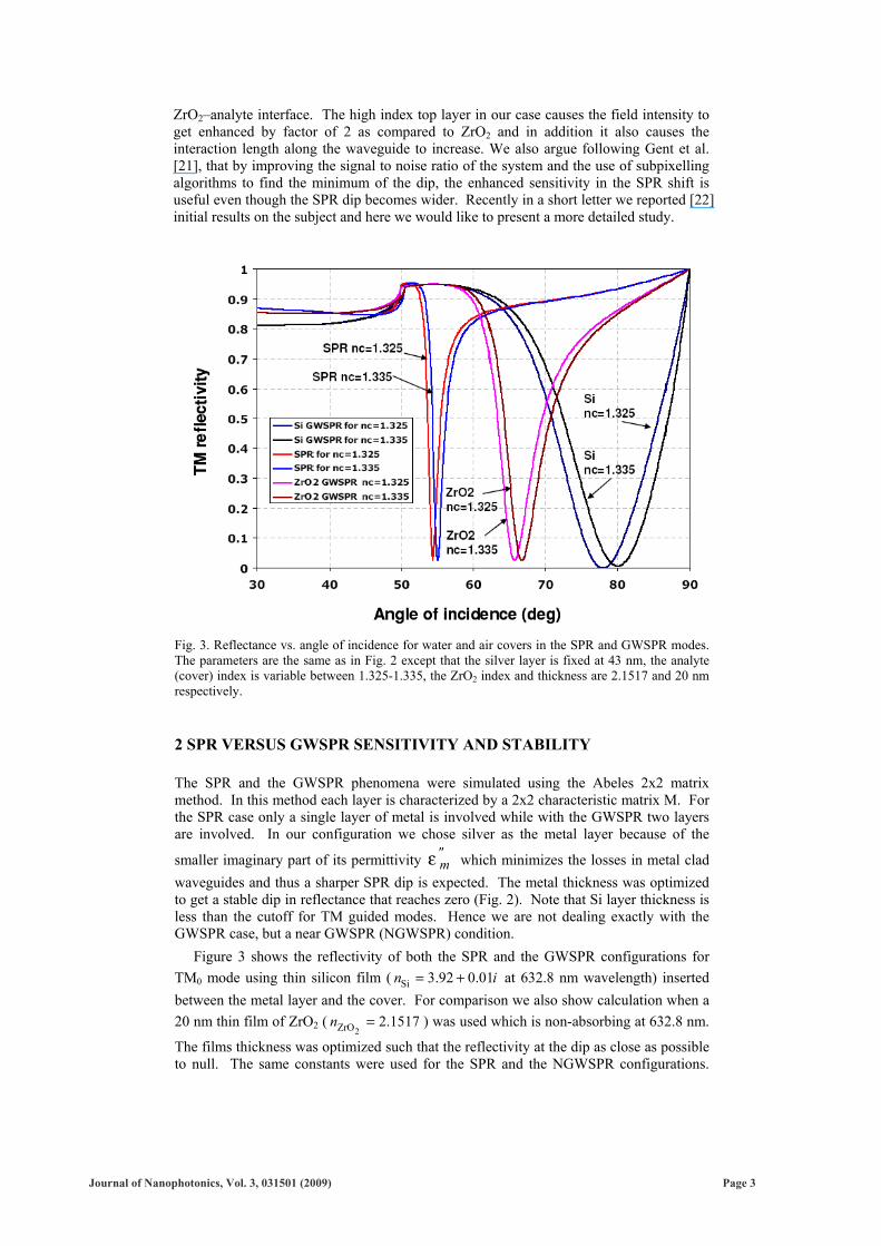
Fig. 2. Reflectance vs. angle of incidence for the SPR and GWSPR modes. Parameters are: wavelength = 632.8 nm, Si film thickness=10 nm, prism index = 1.73205, analyte index = 1.325, silver index = 0.13+3.99i, and Si film index = 3.92+0.01i.
Using the GWSPR configuration with a very thin dielectric material having a high real part of the dielectric constant ′ε as a waveguide layer we achieved better sensitivity and stability of the sensor in comparison to the SPR configuration. Although Gent et al. [21] explained their sensitivity enhancement as originating from field enhancement near the
Analyte
Dielectric film
θp
Metal film
Analyte
Dielectric film
θp
Metal film
Journal of Nanophotonics, Vol. 3, 031501 (2009) Page 2
ZrO2–analyte interface. The high index top layer in our case causes the field intensity to get enhanced by factor of 2 as compared to ZrO2 and in addition it also causes the interaction length along the waveguide to increase. We also argue following Gent et al. [21], that by improving the signal to noise ratio of the system and the use of subpixelling algorithms to find the minimum of the dip, the enhanced sensitivity in the SPR shift is useful even though the SPR dip becomes wider. Recently in a short letter we reported [22] initial results on the subject and here we would like to present a more detailed study.
Fig. 3. Reflectance vs. angle of incidence for water and air covers in the SPR and GWSPR modes. The parameters are the same as in Fig. 2 except that the silver layer is fixed at 43 nm, the analyte (cover) index is variable between 1.325-1.335, the ZrO2 index and thickness are 2.1517 and 20 nm respectively.
2 SPR VERSUS GWSPR SENSITIVITY AND STABILITY
The SPR and the GWSPR phenomena were simulated using the Abeles 2x2 matrix method. In this method each layer is characterized by a 2x2 characteristic matrix M. For the SPR case only a single layer of metal is involved while with the GWSPR two layers are involved. In our configuration we chose silver as the metal layer because of the
smaller imaginary part of its permittivity "mε which minimizes the losses in metal clad
waveguides and thus a sharper SPR dip is expected. The metal thickness was optimized to get a stable dip in reflectance that reaches zero (Fig. 2). Note that Si layer thickness is less than the cutoff for TM guided modes. Hence we are not dealing exactly with the GWSPR case, but a near GWSPR (NGWSPR) condition.
Figure 3 shows the reflectivity of both the SPR and the GWSPR configurations for TM0 mode using thin silicon film ( Si 3.92 0.01n i= + at 632.8 nm wavelength) inserted between the metal layer and the cover. For comparison we also show calculation when a 20 nm thin film of ZrO2 (
2ZrO 2.1517n = ) was used which is non-absorbing at 632.8 nm.
The films thickness was optimized such that the reflectivity at the dip as close as possible to null. The same constants were used for the SPR and the NGWSPR configurations.
Journal of Nanophotonics, Vol. 3, 031501 (2009) Page 3
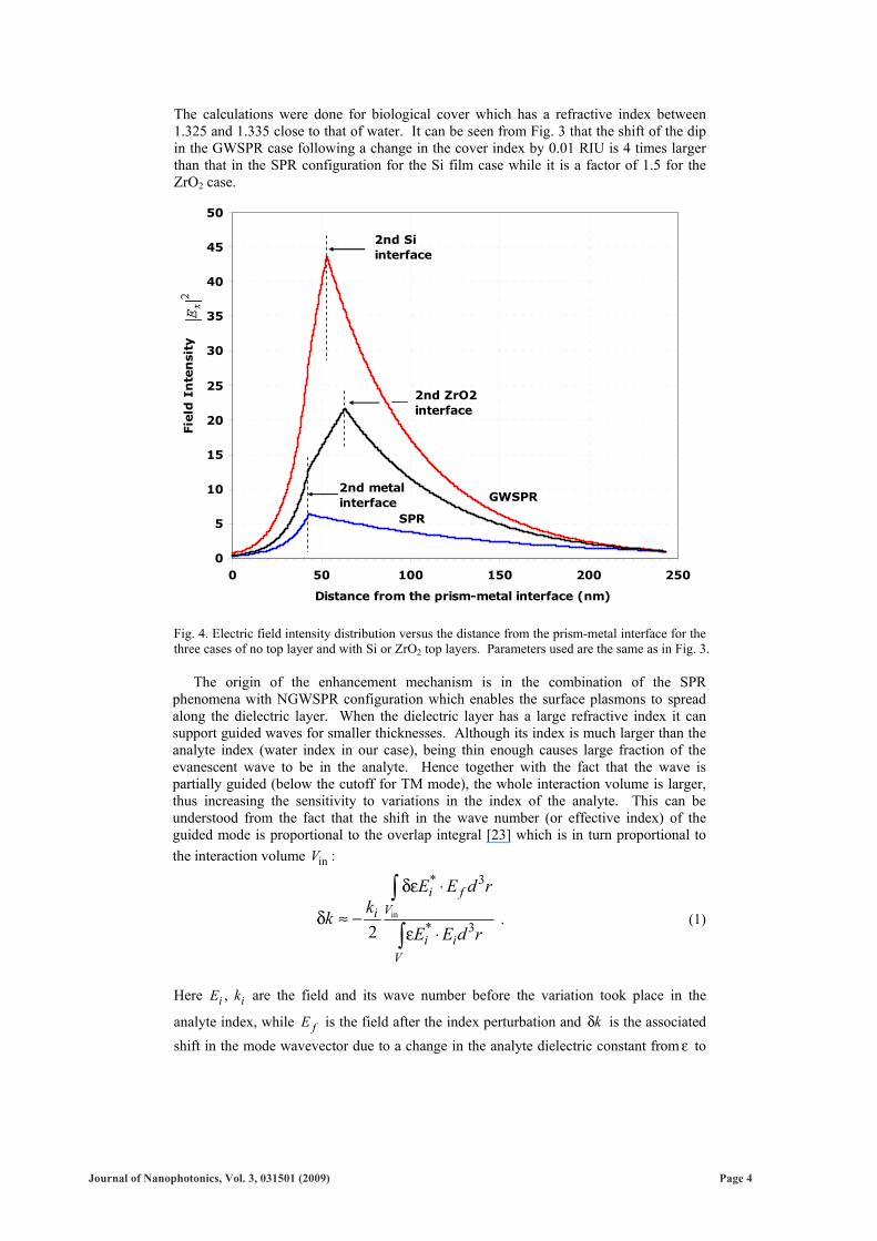
The calculations were done for biological cover which has a refractive index between 1.325 and 1.335 close to that of water. It can be seen from Fig. 3 that the shift of the dip in the GWSPR case following a change in the cover index by 0.01 RIU is 4 times larger than that in the SPR configuration for the Si film case while it is a factor of 1.5 for the ZrO2 case.
0
5
10
15
20
25
30
35
40
45
50
0 50 100 150 200 250
Distance from the prism-metal interface (nm)
Fie
ld I
nte
nsi
ty
SPR
GWSPR2nd metal interface
2nd Si interface
2nd ZrO2 interface
Fig. 4. Electric field intensity distribution versus the distance from the prism-metal interface for the three cases of no top layer and with Si or ZrO2 top layers. Parameters used are the same as in Fig. 3.
The origin of the enhancement mechanism is in the combination of the SPR phenomena with NGWSPR configuration which enables the surface plasmons to spread along the dielectric layer. When the dielectric layer has a large refractive index it can support guided waves for smaller thicknesses. Although its index is much larger than the analyte index (water index in our case), being thin enough causes large fraction of the evanescent wave to be in the analyte. Hence together with the fact that the wave is partially guided (below the cutoff for TM mode), the whole interaction volume is larger, thus increasing the sensitivity to variations in the index of the analyte. This can be understood from the fact that the shift in the wave number (or effective index) of the guided mode is proportional to the overlap integral [23] which is in turn proportional to the interaction volume inV :
in
* 3
* 32
i fVi
i iV
E E d rkk
E E d r
δε ⋅
δ ≈ −ε ⋅
∫
∫ . (1)
Here , i iE k are the field and its wave number before the variation took place in the
analyte index, while fE is the field after the index perturbation and kδ is the associated shift in the mode wavevector due to a change in the analyte dielectric constant from ε to
Journal of Nanophotonics, Vol. 3, 031501 (2009) Page 4
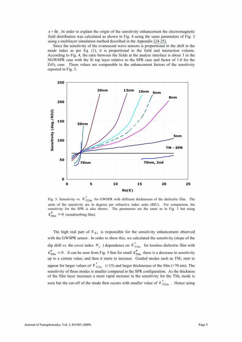
ε + δε . In order to explain the origin of the sensitivity enhancement the electromagnetic field distribution was calculated as shown in Fig. 4 using the same parameters of Fig. 3 using a multilayer simulation method described in the Appendix [24-25].
Since the sensitivity of the evanescent wave sensors is proportional to the shift in the mode index as per Eq. (1), it is proportional to the field and interaction volume. According to Fig. 4, the ratio between the fields at the analyte interface is about 3 in the NGWSPR case with the Si top layer relative to the SPR case and factor of 1.8 for the ZrO2 case. These values are comparable to the enhancement factors of the sensitivity reported in Fig. 3.
0
50
100
150
200
250
0 5 10 15 20 25
Re(Є)
Sen
siti
vit
y (
deg
./R
IU)
TM - SPR
70nm, 2nd
5nm
8nm9nm10nm12nm20nm
50nm
70nm
Fig. 5. Sensitivity vs. f i lm′ε for GWSPR with different thicknesses of the dielectric film. The units of the sensitivity are in degrees per refractive index units (RIU). For comparison, the sensitivity for the SPR is also shown. The parameters are the same as in Fig. 3 but using
film 0′′ε = (nonabsorbing film).
The high real part of S iε is responsible for the sensitivity enhancement observed with the GWSPR sensor. In order to show this, we calculated the sensitivity (slope of the
dip shift vs. the cover index cn ) dependence on fi lm′ε for lossless dielectric film with
film 0′′ε = . It can be seen from Fig. 5 that for small film′′ε there is a decrease in sensitivity up to a certain value, and then it starts to increase. Guided modes such as TM1 start to
appear for larger values of f i lm′ε (>15) and larger thicknesses of the film (>70 nm). The sensitivity of these modes is smaller compared to the SPR configuration. As the thickness of the film layer increases a more rapid increase in the sensitivity for the TM0 mode is
seen but the cut-off of the mode then occurs with smaller value of f i lm′ε . Hence using
Journal of Nanophotonics, Vol. 3, 031501 (2009) Page 5
Si as the film material one expects to observe this behavior due to the high value of S i′ε as a film layer. Doing that allows achieving better sensitivity and better stability of the sensor because Si can act as a protecting layer for silver which otherwise has high interaction with other substances.
30
35
40
45
50
55
60
65
70
0 5 10 15 20 25 30
Re {Є}
Sen
siti
vity
(deg
. /
RIU
)
60 nm
35
28 20 nm
TM - SPR
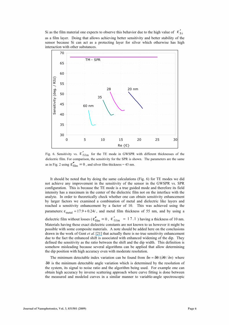
Fig. 6. Sensitivity vs. f i lm′ε for the TE mode in GWSPR with different thicknesses of the dielectric film. For comparison, the sensitivity for the SPR is shown. The parameters are the same as in Fig. 2 using film 0′′ε = , and silver film thickness = 43 nm.
It should be noted that by doing the same calculations (Fig. 6) for TE modes we did not achieve any improvement in the sensitivity of the sensor in the GWSPR vs. SPR configuration. This is because the TE mode is a true guided mode and therefore its field intensity has a maximum in the center of the dielectric film not on the interface with the analyte. In order to theoretically check whether one can obtain sensitivity enhancement by larger factors we examined a combination of metal and dielectric like layers and reached a sensitivity enhancement by a factor of 10. This was achieved using the parameters: metal 17.9 0.24iε = + , and metal film thickness of 55 nm, and by using a
dielectric film without losses ( film 0′′ε = , f i lm 1 7 .1=′ε ) having a thickness of 10 nm. Materials having these exact dielectric constants are not known to us however it might be possible with some composite materials. A note should be added here on the conclusions drawn in the work of Gent et al. [21] that actually there is no true sensitivity enhancement due to the fact the enhanced shift is associated with enhanced widening of the dip. They defined the sensitivity as the ratio between the shift and the dip width. This definition is somehow misleading because several algorithms can be applied that allow determining the dip position with high accuracy even with moderate resolution.
The minimum detectable index variation can be found from /( / )n nδ = δθ ∂θ ∂ where δθ is the minimum detectable angle variation which is determined by the resolution of the system, its signal to noise ratio and the algorithm being used. For example one can obtain high accuracy by inverse scattering approach where curve fitting is done between the measured and modeled curves in a similar manner to variable-angle spectroscopic
Journal of Nanophotonics, Vol. 3, 031501 (2009) Page 6
ellipsometry where one can obtain sub Angstrom accuracy of the layer thicknesses measurement. Another sub-pixelling algorithm used frequently to find minimum or maximum positions of dips and peaks uses fitting the extremum neighborhood to parabolic function. Another possibility is to take the derivative of the dip curve and look for the zero crossing point. We have tried the parabolic fit approach to determine the dip position and found improvement of the sensitivity by a factor of 2 when 1% system error was introduced.
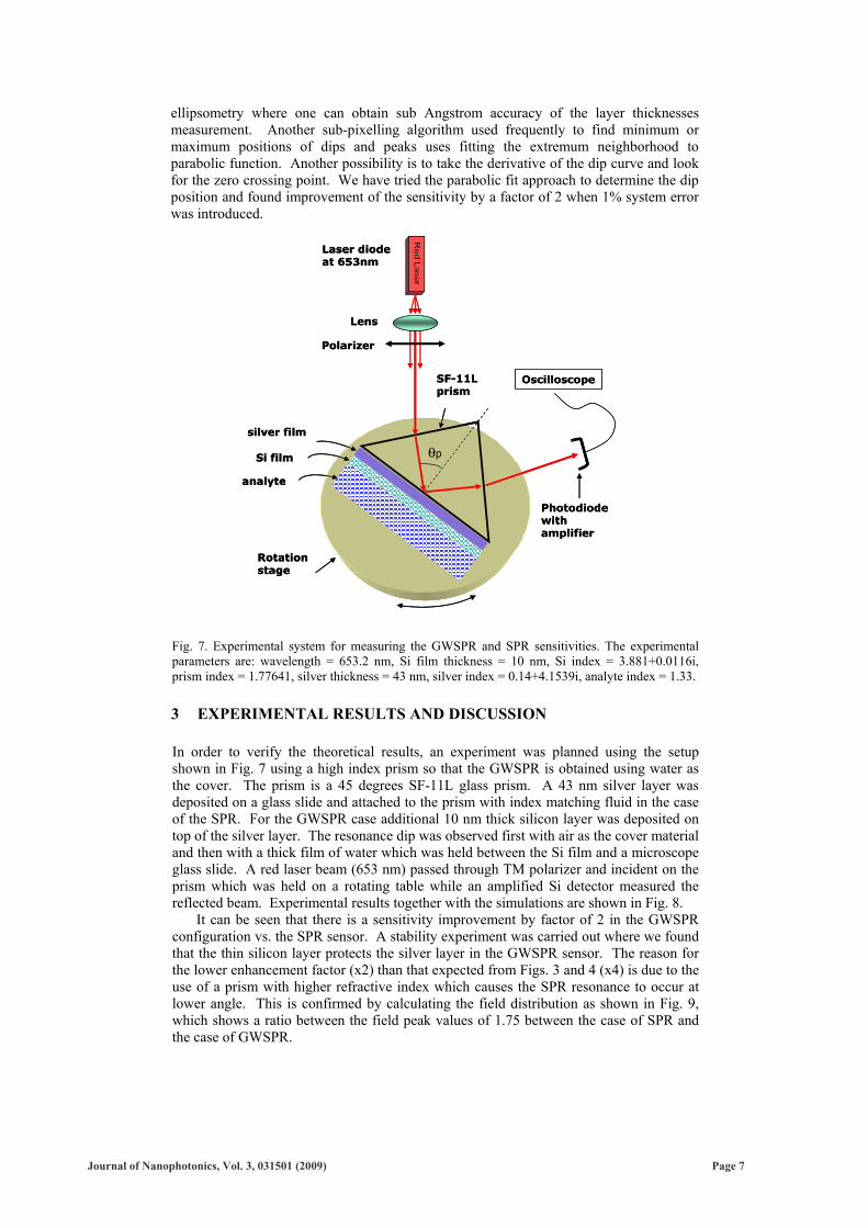
Fig. 7. Experimental system for measuring the GWSPR and SPR sensitivities. The experimental parameters are: wavelength = 653.2 nm, Si film thickness = 10 nm, Si index = 3.881+0.0116i, prism index = 1.77641, silver thickness = 43 nm, silver index = 0.14+4.1539i, analyte index = 1.33.
3 EXPERIMENTAL RESULTS AND DISCUSSION
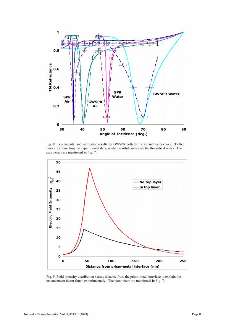
In order to verify the theoretical results, an experiment was planned using the setup shown in Fig. 7 using a high index prism so that the GWSPR is obtained using water as the cover. The prism is a 45 degrees SF-11L glass prism. A 43 nm silver layer was deposited on a glass slide and attached to the prism with index matching fluid in the case of the SPR. For the GWSPR case additional 10 nm thick silicon layer was deposited on top of the silver layer. The resonance dip was observed first with air as the cover material and then with a thick film of water which was held between the Si film and a microscope glass slide. A red laser beam (653 nm) passed through TM polarizer and incident on the prism which was held on a rotating table while an amplified Si detector measured the reflected beam. Experimental results together with the simulations are shown in Fig. 8.
It can be seen that there is a sensitivity improvement by factor of 2 in the GWSPR configuration vs. the SPR sensor. A stability experiment was carried out where we found that the thin silicon layer protects the silver layer in the GWSPR sensor. The reason for the lower enhancement factor (x2) than that expected from Figs. 3 and 4 (x4) is due to the use of a prism with higher refractive index which causes the SPR resonance to occur at lower angle. This is confirmed by calculating the field distribution as shown in Fig. 9, which shows a ratio between the field peak values of 1.75 between the case of SPR and the case of GWSPR.
Laser diode at 653nm
Polarizer
SF-11L prism
silver film
Si film θp
Oscilloscope
Photodiode with amplifier
Rotation stage
Lens
analyte
Laser diode at 653nm
Polarizer
SF-11L prism
silver film
Si film θp
Oscilloscope
Photodiode with amplifier
Rotation stage
Lens
analyte
Journal of Nanophotonics, Vol. 3, 031501 (2009) Page 7
SPRAir
SPRWater
GWSPRAir
GWSPR Water
0
0.2
0.4
0.6
0.8
1
30 40 50 60 70 80 90Angle of Incidence (deg.)
TM
Refl
ect
an
ce
Fig. 8. Experimental and simulation results for GWSPR both for the air and water cover. (Dotted lines are connecting the experimental data, while the solid curves are the theoretical ones). The parameters are mentioned in Fig. 7.
0
5
10
15
20
25
30
35
40
45
50
0 50 100 150 200 250
Distance from prism-metal interface (nm)
Ele
ctri
c Fie
ld I
nte
nsi
ty
No top layer
Si top layer
Fig. 9. Field intensity distribution versus distance from the prism-metal interface to explain the enhancement factor found experimentally. The parameters are mentioned in Fig. 7.
Journal of Nanophotonics, Vol. 3, 031501 (2009) Page 8
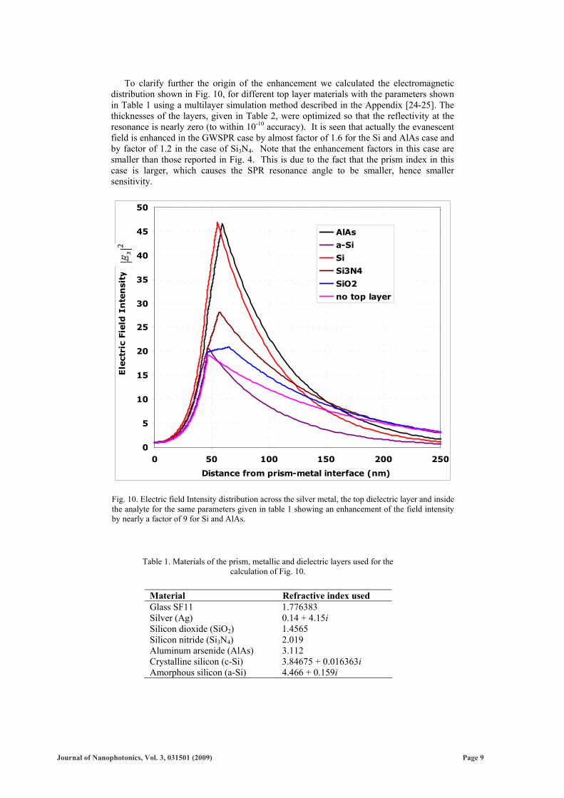
To clarify further the origin of the enhancement we calculated the electromagnetic
distribution shown in Fig. 10, for different top layer materials with the parameters shown in Table 1 using a multilayer simulation method described in the Appendix [24-25]. The thicknesses of the layers, given in Table 2, were optimized so that the reflectivity at the resonance is nearly zero (to within 10-10 accuracy). It is seen that actually the evanescent field is enhanced in the GWSPR case by almost factor of 1.6 for the Si and AlAs case and by factor of 1.2 in the case of Si3N4. Note that the enhancement factors in this case are smaller than those reported in Fig. 4. This is due to the fact that the prism index in this case is larger, which causes the SPR resonance angle to be smaller, hence smaller sensitivity.
0
5
10
15
20
25
30
35
40
45
50
0 50 100 150 200 250
Distance from prism-metal interface (nm)
Ele
ctri
c Fie
ld I
nte
nsi
ty
AlAs
a-Si
Si
Si3N4
SiO2
no top layer
Fig. 10. Electric field Intensity distribution across the silver metal, the top dielectric layer and inside the analyte for the same parameters given in table 1 showing an enhancement of the field intensity by nearly a factor of 9 for Si and AlAs.
Table 1. Materials of the prism, metallic and dielectric layers used for the calculation of Fig. 10.
Material Refractive index used Glass SF11 1.776383 Silver (Ag) 0.14 + 4.15i Silicon dioxide (SiO2) 1.4565 Silicon nitride (Si3N4) 2.019 Aluminum arsenide (AlAs) 3.112 Crystalline silicon (c-Si) 3.84675 + 0.016363i Amorphous silicon (a-Si) 4.466 + 0.159i
Journal of Nanophotonics, Vol. 3, 031501 (2009) Page 9
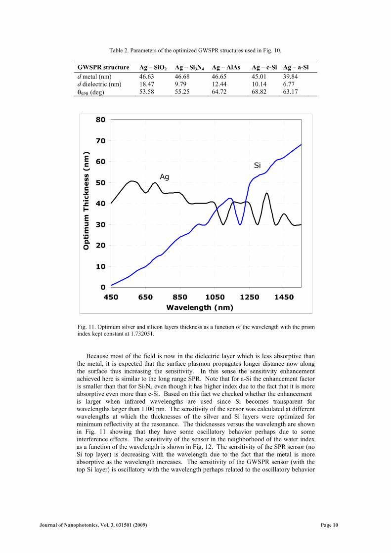
Table 2. Parameters of the optimized GWSPR structures used in Fig. 10.
GWSPR structure Ag – SiO2 Ag – Si3N4 Ag – AlAs Ag – c-Si Ag – a-Si d metal (nm) 46.63 46.68 46.65 45.01 39.84 d dielectric (nm) 18.47 9.79 12.44 10.14 6.77 θSPR (deg) 53.58 55.25 64.72 68.82 63.17
0
10
20
30
40
50
60
70
80
450 650 850 1050 1250 1450Wavelength (nm)
Op
tim
um
Th
ickn
ess
(n
m)
Ag
Si
Fig. 11. Optimum silver and silicon layers thickness as a function of the wavelength with the prism index kept constant at 1.732051.
Because most of the field is now in the dielectric layer which is less absorptive than the metal, it is expected that the surface plasmon propagates longer distance now along the surface thus increasing the sensitivity. In this sense the sensitivity enhancement achieved here is similar to the long range SPR. Note that for a-Si the enhancement factor is smaller than that for Si3N4 even though it has higher index due to the fact that it is more absorptive even more than c-Si. Based on this fact we checked whether the enhancement is larger when infrared wavelengths are used since Si becomes transparent for wavelengths larger than 1100 nm. The sensitivity of the sensor was calculated at different wavelengths at which the thicknesses of the silver and Si layers were optimized for minimum reflectivity at the resonance. The thicknesses versus the wavelength are shown in Fig. 11 showing that they have some oscillatory behavior perhaps due to some interference effects. The sensitivity of the sensor in the neighborhood of the water index as a function of the wavelength is shown in Fig. 12. The sensitivity of the SPR sensor (no Si top layer) is decreasing with the wavelength due to the fact that the metal is more absorptive as the wavelength increases. The sensitivity of the GWSPR sensor (with the top Si layer) is oscillatory with the wavelength perhaps related to the oscillatory behavior
Journal of Nanophotonics, Vol. 3, 031501 (2009) Page 10
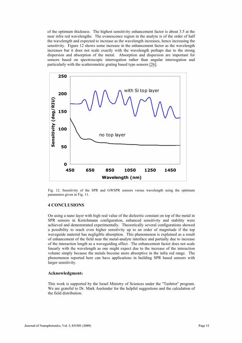
of the optimum thickness. The highest sensitivity enhancement factor is about 3.5 at the near infra red wavelengths. The evanescence region in the analyte is of the order of half the wavelength and expected to increase as the wavelength increases, hence increasing the sensitivity. Figure 12 shows some increase in the enhancement factor as the wavelength increases but it does not scale exactly with the wavelength perhaps due to the strong dispersion and absorption of the metal. Absorption and dispersion are important for sensors based on spectroscopic interrogation rather than angular interrogation and particularly with the scatterometric grating based type sensors [26].
0
50
100
150
200
250
450 650 850 1050 1250 1450
Wavelength (nm)
Sen
siti
vit
y (
deg
/R
IU)
no top layer
with Si top layer
Fig. 12. Sensitivity of the SPR and GWSPR sensors versus wavelength using the optimum parameters given in Fig. 11.
4 CONCLUSIONS
On using a nano layer with high real value of the dielectric constant on top of the metal in SPR sensors in Kretchmann configuration, enhanced sensitivity and stability were achieved and demonstrated experimentally. Theoretically several configurations showed a possibility to reach even higher sensitivity up to an order of magnitude if the top waveguide material has negligible absorption. This phenomenon is explained as a result of enhancement of the field near the metal-analyte interface and partially due to increase of the interaction length as a waveguiding effect. The enhancement factor does not scale linearly with the wavelength as one might expect due to the increase of the interaction volume simply because the metals become more absorptive in the infra red range. The phenomenon reported here can have applications in building SPR based sensors with larger sensitivity.
Acknowledgments
This work is supported by the Israel Ministry of Sciences under the "Tashtiot" program. We are grateful to Dr. Mark Auslender for the helpful suggestions and the calculation of the field distribution.
Journal of Nanophotonics, Vol. 3, 031501 (2009) Page 11
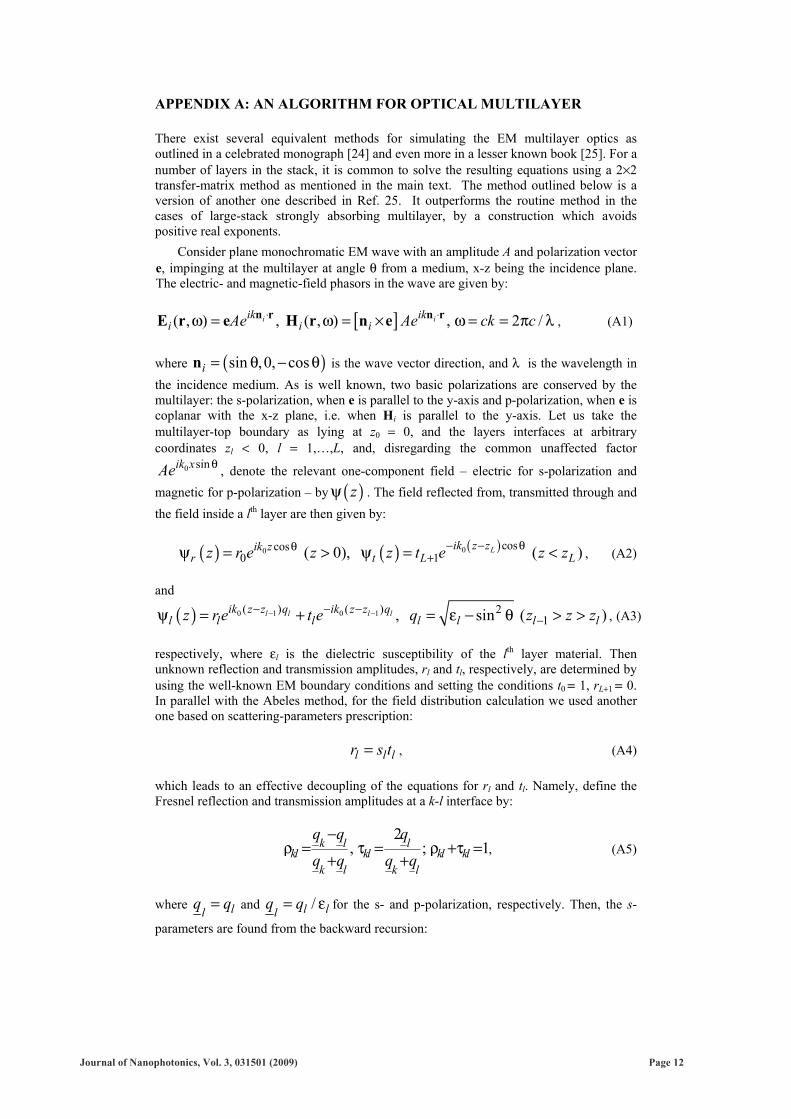
APPENDIX A: AN ALGORITHM FOR OPTICAL MULTILAYER
There exist several equivalent methods for simulating the EM multilayer optics as outlined in a celebrated monograph [24] and even more in a lesser known book [25]. For a number of layers in the stack, it is common to solve the resulting equations using a 2×2 transfer-matrix method as mentioned in the main text. The method outlined below is a version of another one described in Ref. 25. It outperforms the routine method in the cases of large-stack strongly absorbing multilayer, by a construction which avoids positive real exponents.
Consider plane monochromatic EM wave with an amplitude A and polarization vector e, impinging at the multilayer at angle θ from a medium, x-z being the incidence plane. The electric- and magnetic-field phasors in the wave are given by:
[ ]( , ) , ( , ) , 2 /i iik iki i iAe Ae ck c⋅ ⋅ω = ω = × ω = = π λn r n rE r e H r n e , (A1)
where ( )sin ,0, cosi = θ − θn is the wave vector direction, and λ is the wavelength in the incidence medium. As is well known, two basic polarizations are conserved by the multilayer: the s-polarization, when e is parallel to the y-axis and p-polarization, when e is coplanar with the x-z plane, i.e. when Hi is parallel to the y-axis. Let us take the multilayer-top boundary as lying at z0 = 0, and the layers interfaces at arbitrary coordinates zl < 0, l = 1,…,L, and, disregarding the common unaffected factor
0 sinik xAe θ , denote the relevant one-component field – electric for s-polarization and magnetic for p-polarization – by ( )zψ . The field reflected from, transmitted through and the field inside a lth layer are then given by:
( ) ( ) ( )00 coscos0 1 ( 0), ( )Lik z zik z
r t L Lz r e z z t e z z− − θθ+ψ = > ψ = < , (A2)
and
( ) 0 1 0 1( ) ( ) 21, sin ( )l l l lik z z q ik z z q
l l l l l l lz r e t e q z z z− −− − −−ψ = + = ε − θ > > , (A3)
respectively, where εl is the dielectric susceptibility of the lth layer material. Then unknown reflection and transmission amplitudes, rl and tl, respectively, are determined by using the well-known EM boundary conditions and setting the conditions t0 = 1, rL+1 = 0. In parallel with the Abeles method, for the field distribution calculation we used another one based on scattering-parameters prescription:
l l lr s t= , (A4) which leads to an effective decoupling of the equations for rl and tl. Namely, define the Fresnel reflection and transmission amplitudes at a k-l interface by:
2, ; 1k l l
kl kl kl klk l k l
q q q
q q q q
−ρ = τ = ρ +τ =
+ +, (A5)
where ll
q q= and /l llq q= ε for the s- and p-polarization, respectively. Then, the s-
parameters are found from the backward recursion:
Journal of Nanophotonics, Vol. 3, 031501 (2009) Page 12
, 1 1 21
, 1 1, , 1, ,1; 0
1l ll l l ikdq
l Ll l l
ss e l L L s
s+ +
++ +
ρ += = − =
+ρ… , (A6)
where dl is the lth layer thickness (with the agreement dl = 0), and the t-amplitudes from the forward recursive equation:
1,
1 0, 1 1
, 0,2, , ; 11
l likd ql l
l ll l l
et t l L t
s+
++ +
τ= = =
+ρ… . (A7)
After solving Eqs. (A6) and (A7), the reflection and transmission coefficients are calculated by:
2
12
0 , +== LtTsR , (A8)
whereas the inlayer fields are calculated by using Eq. (A3).
References
[1] S. A. Kalele, N. R. Tiwari, S. W. Gosavi, and S. K. Kulkarni, "Plasmon-assisted photonics at the nanoscale," J. Nanophoton. 1, 012501 (2007) [doi:10.1117/1.2748429].
[2] Z. Zalevsky, "Integrated micro and nano photonic dynamic devices: a review," J. Nanophoton. 1, 012504 (2007) [doi:10.1117/1.2795715].
[3] I. Abdulhalim, M. Zourob, and A. Lakhtakia, "Surface plasmon resonance sensors: a mini review," Electromagnetics 28, 213-242 (2008) [doi: 10.1080/02726340801921650].
[4] J. M. Pitarke, V. M. Silkin, E. V. Chulkov, and P. M. Echenique, "Theory of surface plasmons and surface-plasmon polaritons," Rept. Prog. Phys. 70, 1-87 (2007) [doi:10.1088/0034-4885/70/1/R01].
[5] H. Raether, Surface Plasmons on Smooth and Rough Surfaces and on Gratings, Springer, Berlin (1988).
[6] D. Felbacq, "Plasmons go quantum," J. Nanophoton. 2, 020302 (2008) [doi:10.1117/1.2953244].
[7] R. T. Deck, D. Sarid, G. A. Olson, and J. M. Elson, "Coupling between finite electromagnetic beam and long-range surface-plasmon mode," Appl. Opt. 22, 3397-3405 (1983).
[8] G. G. Nenningera, P. TobisÏkab, J. Homola, and S. S. Yee, "Long-range surface plasmons for high-resolution surface plasmon resonance sensors," Sens. Actuat. B: Chem. 74 145-151 (2001) [doi:10.1016/S0925-4005(00)00724-3].
[9] N. Skivesen, R. Horvath, and H. C. Pederson, "Optimization of metal clad waveguide sensors," Sens. Actuat. B: Chem. 106, 668-676 (2005) [doi:10.1016/j.snb.2004.09.014].
[10] X.-C. Yuan, B. H. Ong, Y. G. Tan, D. W. Zhang, R. Irawan, and S. C. Tjin, "Sensitivity-stability-optimized surface plasmon resonance sensing with double metal layers," J. Opt. A: Pure Appl. Opt. 8, 959-963 (2006) [doi:10.1088/1464-4258/8/11/005].
[11] B. H. Ong, X. Yuan, S. C. Tjuin, J. Zhang, and H. M. Ng, "Optimized film thickness for maximum field enhancement of a bimetallic surface plasmon
Journal of Nanophotonics, Vol. 3, 031501 (2009) Page 13
resonance biosensor," Sens. Actuat. B: Chem. 114, 1028–1034 (2006) [doi: 10.1016/j.snb.2005.07.064].
[12] S. Y. Wu and H. P. Ho, "Sensitivity improvement of the surface plasmon resonance optical sensor by using a gold-silver transducing layer," Proc. IEEE Electron Devices Meeting, 63-68 (2002) [doi: 10.1109/HKEDM.2002.1029158].
[13] W. Bin and W. Qing-Kang, "High sensitivity transmission-type SPR sensor by using metallic dielectric mixed gratings," Chin. Phys. Lett. 25, 1668-1671 (2008) [doi:10.1088/0256-307X/25/5/040].
[14] C. J. Alleyne, A. G. Kirk, R. C. McPhedran, N. A. P. Nicorovici, and D. Maystre, "Enhanced SPR sensitivity using periodic metallic structures," Opt. Exp. 15, 8163-8169 (2007) [doi:10.1364/OE.15.008163].
[15] A. V. Kabashin and P. I. Nikitin, "Surface plasmon resonance interferometer for bio- and chemical-sensors," Opt. Commun. 150, 5-8 (1998) [doi:10.1016/S0030-4018(97)00726-8].
[16] S. Y. Wu, H. P. Ho, W. C. Law, C. Lin, and S. K. Kong, "Highly sensitive differential phase-sensitive surface plasmon resonance biosensor based on the Mach–Zehnder configuration," Opt. Lett. 29, 2378-2381 (2004) [doi:10.1364/OL.29.002378].
[17] M. H. Chiu, S. F. Wang, and R. S. Chang, "D-type fiber biosensor based on surface-plasmon resonance technology and heterodyne interferometry," Opt. Lett. 30, 233-236 (2005) [doi:10.1364/OL.30.000233].
[18] H. P. Ho, W. Yuan, C. L. Wong, S. Y. Wu , Y. K. Suen, S. K. Kong, and C. Lin, "Sensitivity enhancement based on application of multi-pass interferometry in phase-sensitive surface plasmon resonance biosensor," Opt. Commun. 275, 491-496 (2007) [doi:10.1016/j.optcom.2007.03.067].
[19] J. Y. Lee, H.-C. Shih, C.-T. Hong, and T. K. Chou, "Measurement of refractive index change by surface plasmon resonance and phase quadrature interferometry," Opt. Commun. 276, 283-287 (2007) [doi:10.1016/j.optcom.2007.04.021].
[20] B. Ran and S. G. Lipson, "Comparison between sensitivities of phase and intensity detection in surface plasmon resonance," Opt. Exp. 14, 5641-4650 (2006) [doi:10.1364/OE.14.005641].
[21] J. van Gent, P. V. Lambeck, H. J. M. Kreuwel, G. J. Gerritsma, E. J. R. Sudholter, D. N. Reinhoudt, and T. J. A. Popma, "Optimization of a chemooptical surface plasmon resonance based sensor," Appl. Opt. 29, 2843-2849 (1990).
[22] A. Lahav, M. Auslender, and I. Abdulhalim, "Sensitivity enhancement of guided wave surface plasmon resonance sensors," Opt. Lett. 33, 2539-2541 (2008) [doi:10.1364/OL.33.002539].
[23] I. Abdulhalim, "Biosensing configurations using guided wave resonant structures," in Optical Waveguide Sensing and Imaging, W. J. Bock, I. Gannot, and S. Tanev, Eds., Springer, Berlin (2008).
[24] O. S. Heavens, Optical Properties of Thin Solid Films, Dover Publications, New York (1991).
[25] Z. Knittl, Optics of Thin Films, Wiley, New York (1976). [26] I. Abdulhalim, M. Auslender, and S. Hava, "Resonant and scatterometric
gratings based nano-photonic structures for biosensing," J. Nanophoton. 1, 011680 (2007) [doi:10.1117/1.2811923].
Journal of Nanophotonics, Vol. 3, 031501 (2009) Page 14
Related Documents