© KEMET Electronics Corporation • P.O. Box 5928 • Greenville, SC 29606 • 864-963-6300 • www.kemet.com C1009_C0G_HV_SMD • 6/27/2017 1 One world. One KEMET Ordering Information C 1210 C 332 J C G A C TU Ceramic Case Size (L" x W") Specification/ Series Capacitance Code (pF) Capacitance Tolerance 1 Rated Voltage (VDC) Dielectric Failure Rate/ Design Termination Finish 2 Packaging/ Grade (C-Spec) 0603 0805 1206 1210 1808 1812 1825 2220 2225 2824 3040 3640 4540 C = Standard Two significant digits and number of zeros. B = ±0.10 pF C = ±0.25 pF D = ±0.5 pF F = ±1% G = ±2% J = ±5% K = ±10% M = ±20% C = 500 B = 630 D = 1,000 F = 1,500 G = 2,000 Z = 2,500 H = 3,000 G = C0G A = N/A C = 100% Matte Sn L = SnPb (5% Pb minimum) See "Packaging C-Spec Ordering Options Table" below 1 Additional capacitance tolerance offerings may be available. Contact KEMET for details. 2 Additional termination finish options may be available. Contact KEMET for details. Surface Mount Multilayer Ceramic Chip Capacitors (SMD MLCCs) High Voltage C0G Dielectric, 500 – 3,000 VDC (Commercial Grade) Overview KEMET’s High Voltage surface mount MLCCs in C0G dielectric feature a 125°C maximum operating temperature and are considered “stable.” The Electronics Industries Alliance (EIA) characterizes C0G dielectric as a Class I material. Components of this classification are temperature compensating and are suited for resonant circuit applications or those where Q and stability of capacitance characteristics are required. C0G exhibits no change in capacitance with respect to time and voltage and boasts a negligible change in capacitance with reference to ambient temperature. Capacitance change is limited to ±30ppm/ºC from −55°C to +125°C. These devices exhibit low ESR at high frequencies and find conventional use as snubbers or filters in applications such as switching power supplies and lighting ballasts. Their exceptional performance at high frequencies has made high voltage MLCC's the preferred dielectric choice of design engineers worldwide. In addition to their use in power supplies, these capacitors are widely used in industries related to automotive(hybrid), telecommunications, medical, military, aerospace, semiconductors and test/diagnostic equipment. In addition to Commercial Grade, Automotive Grade devices are available which meet the demanding Automotive Electronics Council's AEC-Q200 qualification requirements.

Welcome message from author
This document is posted to help you gain knowledge. Please leave a comment to let me know what you think about it! Share it to your friends and learn new things together.
Transcript

© KEMET Electronics Corporation • P.O. Box 5928 • Greenville, SC 29606 • 864-963-6300 • www.kemet.com C1009_C0G_HV_SMD • 6/27/2017 1One world. One KEMET
Ordering InformationC 1210 C 332 J C G A C TU
CeramicCase Size (L" x W")
Specification/Series
Capacitance Code (pF)
Capacitance Tolerance1
Rated Voltage (VDC)
DielectricFailure Rate/
DesignTermination Finish2 Packaging/
Grade (C-Spec)
0603080512061210180818121825222022252824304036404540
C = Standard Two significant digits and number of
zeros.
B = ±0.10 pFC = ±0.25 pFD = ±0.5 pFF = ±1%G = ±2%J = ±5%K = ±10%M = ±20%
C = 500 B = 630 D = 1,000 F = 1,500 G = 2,000 Z = 2,500 H = 3,000
G = C0G A = N/A C = 100% Matte SnL = SnPb (5% Pb minimum)
See"Packaging
C-Spec Ordering Options
Table" below
1 Additional capacitance tolerance offerings may be available. Contact KEMET for details.2 Additional termination finish options may be available. Contact KEMET for details.
Surface Mount Multilayer Ceramic Chip Capacitors (SMD MLCCs)
High Voltage C0G Dielectric, 500 – 3,000 VDC(Commercial Grade)
Overview
KEMET’s High Voltage surface mount MLCCs in C0G dielectric feature a 125°C maximum operating temperature and are considered “stable.” The Electronics Industries Alliance (EIA) characterizes C0G dielectric as a Class I material. Components of this classification are temperature compensating and are suited for resonant circuit applications or those where Q and stability of capacitance characteristics are required. C0G exhibits no change in capacitance with respect to time and voltage and boasts a negligible change in capacitance with reference to ambient temperature. Capacitance change is limited to ±30ppm/ºC from −55°C to +125°C.
These devices exhibit low ESR at high frequencies and find conventional use as snubbers or filters in applications such as switching power supplies and lighting ballasts. Their exceptional performance at high frequencies has made high voltage MLCC's the preferred dielectric choice of design engineers worldwide. In addition to their use in power supplies, these capacitors are widely used in industries related to automotive(hybrid), telecommunications, medical, military, aerospace, semiconductors and test/diagnostic equipment.
In addition to Commercial Grade, Automotive Grade devices are available which meet the demanding Automotive Electronics Council's AEC-Q200 qualification requirements.

© KEMET Electronics Corporation • P.O. Box 5928 • Greenville, SC 29606 • 864-963-6300 • www.kemet.com C1009_C0G_HV_SMD • 6/27/2017 2
Surface Mount Multilayer Ceramic Chip Capacitors (SMD MLCCs)High Voltage C0G Dielectric, 500 – 3,000 VDC (Commercial Grade)
Packaging C-Spec Ordering Options Table
Packaging Type1 Packaging/Grade Ordering Code (C-Spec)
Bulk Bag/Unmarked Not required (Blank)7" Reel/Unmarked TU
13" Reel/Unmarked 7411 (EIA 0603 and smaller case sizes)7210 (EIA 0805 and larger case sizes)
7" Reel/Unmarked/2 mm pitch2 708113" Reel/Unmarked/2 mm pitch2 7082
1 Default packaging is “Bulk Bag”. An ordering code C-Spec is not required for “Bulk Bag” packaging.1 "Bulk Bag" packaging option is not available for case sizes larger than 2225 (5664 Metric).1 The terms “Marked” and “Unmarked” pertain to laser marking option of capacitors. All packaging options labeled as “Unmarked” will contain
capacitors that have not been laser marked. The option to laser mark is not available on these devices. For more information see “Capacitor Marking”.2 The 2 mm pitch option allows for double the packaging quantity of capacitors on a given reel size. This option is limited to EIA 0603 (1608 metric) case
size devices. For more information regarding 2 mm pitch option see “Tape & Reel Packaging Information”.
Benefits
• Operating temperature range of −55°C to +125°C• Lead (Pb)-Free, RoHS and REACH compliant• EIA 0603, 0805, 1206, 1210, 1808, 1812, 1825, 2220,
2225, 2824, 3040, 3640 and 4540 case sizes• DC voltage ratings of 500 V, 630 V, 1 KV, 1.5 KV, 2 KV,
2.5 KV and 3 KV• Capacitance offerings ranging from 1pF to 0.150μF• Available capacitance tolerances of ±0.10pF, ±0.25pF,
±0.5pF, ±1%, ±2%, ±5%, ±10% and ±20%• No piezoelectric noise• Extremely low ESR and ESL• High thermal stability• High ripple current capability
• Preferred capacitance solution at line frequencies and into the MHz range
• No capacitance change with respect to applied rated DC voltage
• Negligible capacitance change with respect to temperature from −55°C to +125°C
• No capacitance decay with time• Non-polar device, minimizing installation concerns• Automotive (AEC–Q200) grade available • 100% pure matte tin-plated termination finish allowing
for excellent solderability• SnPb plated termination finish option available upon
request (5% Pb minimum)
Applications
Typical applications include switch mode power supplies (input filters, resonators, tank circuits, snubbed circuits, output filters), high voltage coupling and DC blocking, lighting ballasts, voltage multiplier circuits, DC/DC converters and coupling capacitors in Ćuk converters. Markets include power supply, LCD fluorescent backlight ballasts, HID lighting, telecom equipment, industrial and medical equipment/control, LAN/WAN interface, analog and digital modems, and automotive.
© KEMET Electronics Corporation • P.O. Box 5928 • Greenville, SC 29606 • 864-963-6300 • www.kemet.com C1009_C0G_HV_SMD • 6/27/2017 3
Surface Mount Multilayer Ceramic Chip Capacitors (SMD MLCCs)High Voltage C0G Dielectric, 500 – 3,000 VDC (Commercial Grade)
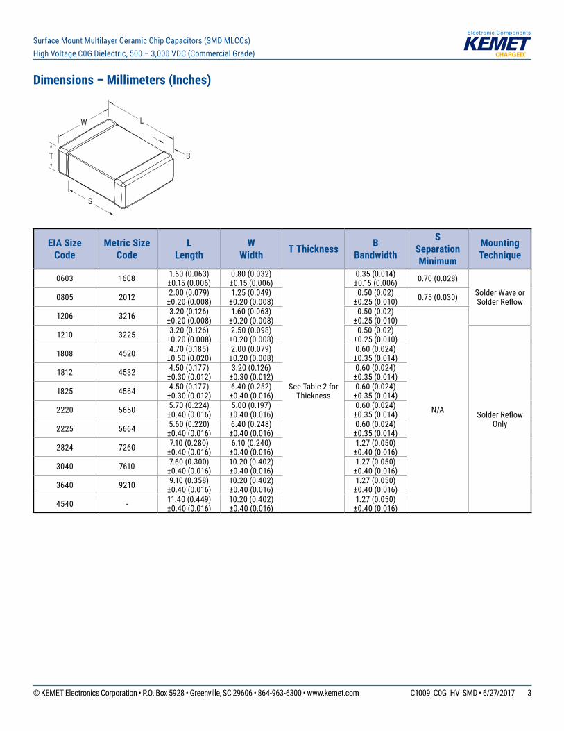
Dimensions – Millimeters (Inches)
L
B
W
S
T
EIA Size Code
Metric Size Code
L Length
W Width T Thickness B
Bandwidth
SSeparation Minimum
Mounting Technique
0603 1608 1.60 (0.063) ±0.15 (0.006)
0.80 (0.032) ±0.15 (0.006)
See Table 2 for Thickness
0.35 (0.014) ±0.15 (0.006) 0.70 (0.028)
Solder Wave or Solder Reflow0805 2012 2.00 (0.079)
±0.20 (0.008)1.25 (0.049)
±0.20 (0.008)0.50 (0.02)
±0.25 (0.010) 0.75 (0.030)
1206 3216 3.20 (0.126) ±0.20 (0.008)
1.60 (0.063) ±0.20 (0.008)
0.50 (0.02) ±0.25 (0.010)
N/A
1210 3225 3.20 (0.126) ±0.20 (0.008)
2.50 (0.098) ±0.20 (0.008)
0.50 (0.02) ±0.25 (0.010)
Solder Reflow Only
1808 4520 4.70 (0.185) ±0.50 (0.020)
2.00 (0.079) ±0.20 (0.008)
0.60 (0.024) ±0.35 (0.014)
1812 4532 4.50 (0.177) ±0.30 (0.012)
3.20 (0.126) ±0.30 (0.012)
0.60 (0.024) ±0.35 (0.014)
1825 4564 4.50 (0.177) ±0.30 (0.012)
6.40 (0.252) ±0.40 (0.016)
0.60 (0.024) ±0.35 (0.014)
2220 5650 5.70 (0.224) ±0.40 (0.016)
5.00 (0.197) ±0.40 (0.016)
0.60 (0.024) ±0.35 (0.014)
2225 5664 5.60 (0.220) ±0.40 (0.016)
6.40 (0.248) ±0.40 (0.016)
0.60 (0.024) ±0.35 (0.014)
2824 7260 7.10 (0.280) ±0.40 (0.016)
6.10 (0.240) ±0.40 (0.016)
1.27 (0.050) ±0.40 (0.016)
3040 7610 7.60 (0.300) ±0.40 (0.016)
10.20 (0.402) ±0.40 (0.016)
1.27 (0.050) ±0.40 (0.016)
3640 9210 9.10 (0.358) ±0.40 (0.016)
10.20 (0.402) ±0.40 (0.016)
1.27 (0.050) ±0.40 (0.016)
4540 - 11.40 (0.449) ±0.40 (0.016)
10.20 (0.402) ±0.40 (0.016)
1.27 (0.050) ±0.40 (0.016)

© KEMET Electronics Corporation • P.O. Box 5928 • Greenville, SC 29606 • 864-963-6300 • www.kemet.com C1009_C0G_HV_SMD • 6/27/2017 4
Surface Mount Multilayer Ceramic Chip Capacitors (SMD MLCCs)High Voltage C0G Dielectric, 500 – 3,000 VDC (Commercial Grade)
Qualification/Certification
Commercial Grade products are subject to internal qualification. Details regarding test methods and conditions are referenced in Table 4, Performance & Reliability.
Environmental Compliance
Lead (Pb)-free, RoHS, and REACH compliant without exemptions (excluding SnPb termination finish option).
Electrical Parameters/Characteristics
Item Parameters/CharacteristicsOperating Temperature Range −55°C to +125°C
Capacitance Change with Reference to +25°C and 0 VDC Applied (TCC) ±30 ppm/ºC
Aging Rate (Maximum % Capacitance Loss/Decade Hour) 0%
1Dielectric Withstanding Voltage (DWV) See Dielectric Withstanding Voltage (DWV) Table(5 ±1 seconds and charge/discharge not exceeding 50 mA)
2Dissipation Factor (DF) Maximum Limit at 25ºC 0.1%
3Insulation Resistance (IR) Limit at 25°C 1,000 megohm microfarads or 100 GΩ(500 VDC applied for 120 ±5 seconds at 25°C)
1DWV is the voltage a capacitor can withstand (survive) for a short period of time. It exceeds the nominal and continuous working voltage of the capacitor.
2Capacitance and dissipation factor (DF) measured under the following conditions: 1 MHz ±100 kHz and 1.0 Vrms ±0.2 V if capacitance ≤ 1,000 pF 1 kHz ±50 Hz and 1.0 Vrms ±0.2 V if capacitance > 1,000 pF3To obtain IR limit, divide MΩ-µF value by the capacitance and compare to GΩ limit. Select the lower of the two limits.Note: When measuring capacitance it is important to ensure the set voltage level is held constant. The HP4284 and Agilent E4980 have a feature known as Automatic Level Control (ALC). The ALC feature should be switched to "ON."

© KEMET Electronics Corporation • P.O. Box 5928 • Greenville, SC 29606 • 864-963-6300 • www.kemet.com C1009_C0G_HV_SMD • 6/27/2017 5
Surface Mount Multilayer Ceramic Chip Capacitors (SMD MLCCs)High Voltage C0G Dielectric, 500 – 3,000 VDC (Commercial Grade)
Dielectric Withstanding Voltage (DWV)
EIA Case Size 500V 630V ≥ 1000V0603
150% of rated voltage
130% of rated voltage
120% of rated voltage
0805 < 620pF 150% of rated voltage ≥ 620pF 130% of rated voltage
1206 < 5.1nF 150% of rated voltage ≥ 5.1nF 130% of rated voltage
1210 < 7.5nF 150% of rated voltage ≥ 7.5nF 130% of rated voltage
1808 < 5.1nF 150% of rated voltage ≥ 5.1nF 130% of rated voltage
1812 < 12nF 150% of rated voltage ≥ 12nF 130% of rated voltage
≥1825 150% of rated voltage
Post Environmental Limits
High Temperature Life, Biased Humidity, Moisture Resistance
DielectricRated DCVoltage
CapacitanceValue
Dissipation Factor (Maximum %)
CapacitanceShift
Insulation Resistance
C0G All All 0.5 0.3% or ±0.25 pF 10% of Initial Limit

© KEMET Electronics Corporation • P.O. Box 5928 • Greenville, SC 29606 • 864-963-6300 • www.kemet.com C1009_C0G_HV_SMD • 6/27/2017 6
Surface Mount Multilayer Ceramic Chip Capacitors (SMD MLCCs)High Voltage C0G Dielectric, 500 – 3,000 VDC (Commercial Grade)
Table 1A – Capacitance Range/Selection Waterfall (0603 – 1808 Case Sizes)
*Capacitance range Includes E24 decade values only. (i.e., 10, 11, 12, 13, 15, 16, 18, 20, 22, 24, 27, 30, 33, 36, 39, 43, 47, 51, 56, 62, 68, 75, 82 and 91)KEMET reserves the right to substitute product with an improved temperature characteristic, tighter capacitance tolerance and/or higher voltage capability within the same form factor (configuration and dimensions).These products are protected under US Patents 7,172,985 and 7,670,981, other patents pending, and any foreign counterparts.
Capacitance Cap Code
Case Size/Series C0603C C0805C C1206C C1210C C1808CVoltage Code C B D C B D C B D F G C B D F G C B D F G Z H
Rated Voltage (VDC) 500
630
1000
500
630
1000
500
630
1000
1500
2000
500
630
1000
1500
2000
500
630
1000
1500
2000
2500
3000
Capacitance Tolerance
Product Availability and Chip Thickness Codes See Table 2 for Chip Thickness Dimensions
1.0 - 9.1 pF* 109 - 919* B C D DG DG DG LB LB LB LB LB LB LB10 pF - 47pF* 100 - 470* F G J K M DG DG DG ED ED ED ED ED FM FM FM FM FM LB LB LB LB LB LB LB
11 pF 110 F G J K M DG DG DG ED ED ED ED ED FM FM FM FM FM LB LB LB LB LB LB LB12 pF 120 F G J K M DG DG DG ED ED ED ED ED FM FM FM FM FM LB LB LB LB LB LB LB13 pF 130 F G J K M DG DG DG ED ED ED ED ED FM FM FM FM FM LB LB LB LB LB LB LB15 pF 150 F G J K M DG DG DG ED ED ED ED ED FM FM FM FM FM LB LB LB LB LB LB LB16 pF 160 F G J K M DG DG DG ED ED ED ED ED FM FM FM FM FM LB LB LB LB LB LB LB18 pF 180 F G J K M DG DG DG ED ED ED ED ED FM FM FM FM FM LB LB LB LB LB LB LB20 pF 200 F G J K M DG DG DG ED ED ED ED ED FM FM FM FM FM LB LB LB LB LB LB LB22 pF 220 F G J K M DG DG DG ED ED ED ED ED FM FM FM FM FM LB LB LB LB LB LB LB24 pF 240 F G J K M DG DG DG ED ED ED ED ED FM FM FM FM FM LB LB LB LB LB LB LB27 pF 270 F G J K M DG DG DG ED ED ED ED ED FM FM FM FM FM LB LB LB LB LB LB LB30 pF 300 F G J K M DG DG DG ED ED ED ED ED FM FM FM FM FM LB LB LB LB LB LB LB33 pF 330 F G J K M DG DG DG ED ED ED ED ED FM FM FM FM FM LB LB LB LB LB LB LB36 pF 360 F G J K M DG DG DG ED ED ED ED ED FM FM FM FM FM LB LB LB LB LB LB LB39 pF 390 F G J K M DG DG DG ED ED ED ED ED FM FM FM FM FM LB LB LB LB LB LB LB43 pF 430 F G J K M DG DG DG ED ED ED ED ED FM FM FM FM FM LB LB LB LB LB LB LB47 pF 470 F G J K M DG DG DG ED ED ED ED ED FM FM FM FM FM LB LB LB LB LB LB LB51 pF 510 F G J K M DG DG DG ED ED ED ED ED FM FM FM FM FM LB LB LB LB LB LB LB56 pF 560 F G J K M DG DG DG ED ED ED ED ED FM FM FM FM FM LB LB LB LB LB LB LB62 pF 620 F G J K M DG DG DG ED ED ED ED ED FM FM FM FM FM LB LB LB LB LB LB LB68 pF 680 F G J K M DG DG DG ED ED ED ED ED FM FM FM FM FM LB LB LB LB LB LB LB75 pF 750 F G J K M DG DG DG ED ED ED ED EF FM FM FM FM FM LB LB LB LB LB LB LB82 pF 820 F G J K M DG DG DG ED ED ED ED EF FM FM FM FM FM LB LB LB LB LB LB LB91 pF 910 F G J K M DG DG DG ED ED ED ED EF FM FM FM FM FM LB LB LB LB LB LB LB
100 pF 101 F G J K M CG CG CG DG DG DG ED ED ED ED EF FM FM FM FM FM LB LB LB LB LB LC LB110 pF 111 F G J K M CG CG CG DG DG DG ED ED ED ED EG FM FM FM FM FM LB LB LB LB LB LC LB120 pF 121 F G J K M CG CG CG DG DG DG ED ED ED ED EG FG FG FG FM FM LA LA LA LA LB LC LB130 pF 131 F G J K M CG CG CG DG DG DG ED ED ED ED EG FG FG FG FM FM LA LA LA LA LB LC LC150 pF 151 F G J K M CG CG CG DG DG DG ED ED ED EF EG FG FG FG FM FM LA LA LA LA LB LC LC160 pF 161 F G J K M CG CG CG DG DG DG ED ED ED EF EG FG FG FG FM FM LA LA LA LA LC LC LC180 pF 181 F G J K M CG CG CG DG DG DG ED ED ED EF EG FG FG FG FM FM LA LA LA LA LC LC LC200 pF 201 F G J K M CG CG CG DG DG DG ED ED ED EF EG FG FG FG FM FM LA LA LA LA LC LC220 pF 221 F G J K M CG CG CG DG DG DG ED ED ED EG EG FG FG FG FM FM LA LA LA LA LC LC240 pF 241 F G J K M CG CG DG DG DG ED ED ED EG EG FG FG FG FM FM LA LA LA LB LC LC270 pF 271 F G J K M CG CG DG DG DG ED ED ED EG EG FG FG FG FK FK LA LA LA LB LC LC300 pF 301 F G J K M CG CG DG DG DN ED ED EF EG FG FG FG FK FK LA LA LA LB LC LC330 pF 331 F G J K M CG CG DG DG DN ED ED EF EG FG FG FG FK FK LA LA LA LB LC LC360 pF 361 F G J K M CG CG DG DG DN ED ED EF EG FG FG FG FK FS LA LA LA LB LA LC390 pF 391 F G J K M CG CG DG DG DN ED ED EF EG FG FG FG FK FS LA LA LA LB LA LC430 pF 431 F G J K M CG CG DG DG DP ED ED EF EG FG FM FM FS FS LA LB LB LC LA470 pF 471 F G J K M CG CG DG DG DP ED ED EG EG FG FM FM FS FS LA LB LB LC LA510 pF 511 F G J K M CG CG DG DG DP ED ED EG EG FG FM FM FS FS LA LB LB LC LB560 pF 561 F G J K M CG CG DG DG DG ED ED EG EG FG FM FM FS FS LA LB LB LC LB620 pF 621 F G J K M CG CG DG DG DG ED ED EG FG FM FM FS FS LA LB LB LA LC680 pF 681 F G J K M CG CG DG DG DG ED ED EG FG FM FM FS FS LB LB LB LA LC750 pF 751 F G J K M DG DG DG ED EF EG FG FM FM FM LB LB LB LA820 pF 821 F G J K M DG DG DG ED EF EG FG FM FM FM LB LB LB LA910 pF 911 F G J K M DN DN ED EF EG FM FM FM FY LB LB LB LA
1,000 pF 102 F G J K M DN DN ED EF EG FM FM FM FY LB LB LB LB1,100 pF 112 F G J K M DN DN EF EG ED FM FK FK FS LC LC LC LB
Capacitance Cap Code
Rated Voltage (VDC) 500
630
1000
500
630
1000
500
630
1000
1500
2000
500
630
1000
1500
2000
500
630
1000
1500
2000
2500
3000
Voltage Code C B D C B D C B D F G C B D F G C B D F G Z H
Case Size/Series C0603C C0805C C1206C C1210C C1808C
© KEMET Electronics Corporation • P.O. Box 5928 • Greenville, SC 29606 • 864-963-6300 • www.kemet.com C1009_C0G_HV_SMD • 6/27/2017 7
Surface Mount Multilayer Ceramic Chip Capacitors (SMD MLCCs)High Voltage C0G Dielectric, 500 – 3,000 VDC (Commercial Grade)
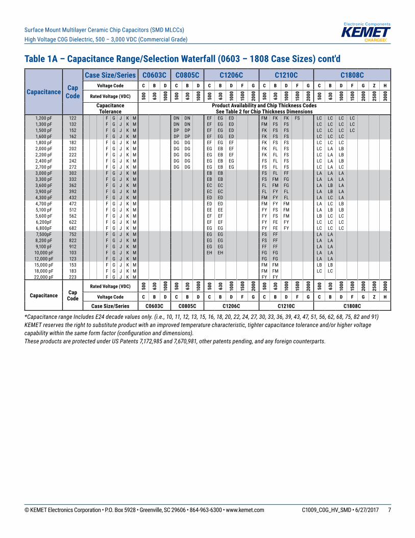
Table 1A – Capacitance Range/Selection Waterfall (0603 – 1808 Case Sizes) cont'd
*Capacitance range Includes E24 decade values only. (i.e., 10, 11, 12, 13, 15, 16, 18, 20, 22, 24, 27, 30, 33, 36, 39, 43, 47, 51, 56, 62, 68, 75, 82 and 91)KEMET reserves the right to substitute product with an improved temperature characteristic, tighter capacitance tolerance and/or higher voltage capability within the same form factor (configuration and dimensions).These products are protected under US Patents 7,172,985 and 7,670,981, other patents pending, and any foreign counterparts.
Capacitance Cap Code
Case Size/Series C0603C C0805C C1206C C1210C C1808CVoltage Code C B D C B D C B D F G C B D F G C B D F G Z H
Rated Voltage (VDC) 500
630
1000
500
630
1000
500
630
1000
1500
2000
500
630
1000
1500
2000
500
630
1000
1500
2000
2500
3000
Capacitance Tolerance
Product Availability and Chip Thickness Codes See Table 2 for Chip Thickness Dimensions
1,200 pF 122 F G J K M DN DN EF EG ED FM FK FK FS LC LC LC LC1,300 pF 132 F G J K M DN DN EF EG ED FM FS FS LC LC LC LC1,500 pF 152 F G J K M DP DP EF EG ED FK FS FS LC LC LC LC1,600 pF 162 F G J K M DP DP EF EG ED FK FS FS LC LC LC1,800 pF 182 F G J K M DG DG EF EG EF FK FS FS LC LC LC2,000 pF 202 F G J K M DG DG EG EB EF FK FL FS LC LA LB2,200 pF 222 F G J K M DG DG EG EB EF FK FL FS LC LA LB2,400 pF 242 F G J K M DG DG EG EB EG FS FL FS LC LA LB2,700 pF 272 F G J K M DG DG EG EB EG FS FL FS LC LA LC3,000 pF 302 F G J K M EB EB FS FL FF LA LA LA3,300 pF 332 F G J K M EB EB FS FM FG LA LA LA3,600 pF 362 F G J K M EC EC FL FM FG LA LB LA3,900 pF 392 F G J K M EC EC FL FY FL LA LB LA4,300 pF 432 F G J K M ED ED FM FY FL LA LC LA4,700 pF 472 F G J K M ED ED FM FY FM LA LC LB5,100 pF 512 F G J K M EE EE FY FS FM LA LB LB5,600 pF 562 F G J K M EF EF FY FS FM LB LC LC6,200pF 622 F G J K M EF EF FY FE FY LC LC LC6,800pF 682 F G J K M EG EG FY FE FY LC LC LC7,500pF 752 F G J K M EG EG FS FF LA LA8,200 pF 822 F G J K M EG EG FS FF LA LA9,100 pF 912 F G J K M EG EG FF FF LA LA
10,000 pF 103 F G J K M EH EH FG FG LA LA12,000 pF 123 F G J K M FG FG LA LA15,000 pF 153 F G J K M FM FM LB LB18,000 pF 183 F G J K M FM FM LC LC22,000 pF 223 F G J K M FY FY
Capacitance Cap Code
Rated Voltage (VDC) 500
630
1000
500
630
1000
500
630
1000
1500
2000
500
630
1000
1500
2000
500
630
1000
1500
2000
2500
3000
Voltage Code C B D C B D C B D F G C B D F G C B D F G Z H
Case Size/Series C0603C C0805C C1206C C1210C C1808C
© KEMET Electronics Corporation • P.O. Box 5928 • Greenville, SC 29606 • 864-963-6300 • www.kemet.com C1009_C0G_HV_SMD • 6/27/2017 8
Surface Mount Multilayer Ceramic Chip Capacitors (SMD MLCCs)High Voltage C0G Dielectric, 500 – 3,000 VDC (Commercial Grade)
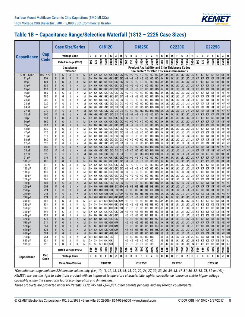
Table 1B – Capacitance Range/Selection Waterfall (1812 – 2225 Case Sizes)
*Capacitance range Includes E24 decade values only. (i.e., 10, 11, 12, 13, 15, 16, 18, 20, 22, 24, 27, 30, 33, 36, 39, 43, 47, 51, 56, 62, 68, 75, 82 and 91)KEMET reserves the right to substitute product with an improved temperature characteristic, tighter capacitance tolerance and/or higher voltage capability within the same form factor (configuration and dimensions).These products are protected under US Patents 7,172,985 and 7,670,981, other patents pending, and any foreign counterparts.
Capacitance Cap Code
Case Size/Series C1812C C1825C C2220C C2225C
Voltage Code C B D F G Z H C B D F G Z H C B D F G Z H C B D F G Z H
Rated Voltage (VDC) 500
630
1000
1500
2000
2500
3000
500
630
1000
1500
2000
2500
3000
500
630
1000
1500
2000
2500
3000
500
630
1000
1500
2000
2500
3000
CapacitanceTolerance
Product Availability and Chip Thickness Codes See Table 2 for Chip Thickness Dimensions
10 pF - 47pF* 100 - 470* F G J K M GK GK GK GK GK GK GK HG HG HG HG HG HG HG JK JK JK JK JK JK JK KF KF KF KF KF KF KF11 pF 110 F G J K M GK GK GK GK GK GK GK HG HG HG HG HG HG HG JK JK JK JK JK JK JK KF KF KF KF KF KF KF12 pF 120 F G J K M GK GK GK GK GK GK GK HG HG HG HG HG HG HG JK JK JK JK JK JK JK KF KF KF KF KF KF KF13 pF 130 F G J K M GK GK GK GK GK GK GK HG HG HG HG HG HG HG JK JK JK JK JK JK JK KF KF KF KF KF KF KF15 pF 150 F G J K M GK GK GK GK GK GK GK HG HG HG HG HG HG HG JK JK JK JK JK JK JK KF KF KF KF KF KF KF16 pF 160 F G J K M GK GK GK GK GK GK GK HG HG HG HG HG HG HG JK JK JK JK JK JK JK KF KF KF KF KF KF KF18 pF 180 F G J K M GK GK GK GK GK GK GK HG HG HG HG HG HG HG JK JK JK JK JK JK JK KF KF KF KF KF KF KF20 pF 200 F G J K M GK GK GK GK GK GK GK HG HG HG HG HG HG HG JK JK JK JK JK JK JK KF KF KF KF KF KF KF22 pF 220 F G J K M GK GK GK GK GK GK GK HG HG HG HG HG HG HG JK JK JK JK JK JK JK KF KF KF KF KF KF KF24 pF 240 F G J K M GK GK GK GK GK GK GK HG HG HG HG HG HG HG JK JK JK JK JK JK JK KF KF KF KF KF KF KF27 pF 270 F G J K M GK GK GK GK GK GK GK HG HG HG HG HG HG HG JK JK JK JK JK JK JK KF KF KF KF KF KF KF30 pF 300 F G J K M GK GK GK GK GK GK GK HG HG HG HG HG HG HG JK JK JK JK JK JK JK KF KF KF KF KF KF KF33 pF 330 F G J K M GK GK GK GK GK GK GK HG HG HG HG HG HG HG JK JK JK JK JK JK JK KF KF KF KF KF KF KF36 pF 360 F G J K M GK GK GK GK GK GK GK HG HG HG HG HG HG HG JK JK JK JK JK JK JK KF KF KF KF KF KF KF39 pF 390 F G J K M GK GK GK GK GK GK GK HG HG HG HG HG HG HG JK JK JK JK JK JK JK KF KF KF KF KF KF KF43 pF 430 F G J K M GK GK GK GK GK GK GK HG HG HG HG HG HG HG JK JK JK JK JK JK JK KF KF KF KF KF KF KF47 pF 470 F G J K M GK GK GK GK GK GK GK HG HG HG HG HG HG HG JK JK JK JK JK JK JK KF KF KF KF KF KF KF51 pF 510 F G J K M GK GK GK GK GK GK GK HG HG HG HG HG HG HG JK JK JK JK JK JK JK KF KF KF KF KF KF KF56 pF 560 F G J K M GK GK GK GK GK GK GK HG HG HG HG HG HG HG JK JK JK JK JK JK JK KF KF KF KF KF KF KF62 pF 620 F G J K M GK GK GK GK GK GK GK HG HG HG HG HG HG HG JK JK JK JK JK JK JK KF KF KF KF KF KF KF68 pF 680 F G J K M GK GK GK GK GK GK GK HG HG HG HG HG HG HG JK JK JK JK JK JK JK KF KF KF KF KF KF KF75 pF 750 F G J K M GK GK GK GK GK GK GK HG HG HG HG HG HG HG JK JK JK JK JK JK JK KF KF KF KF KF KF KF82 pF 820 F G J K M GK GK GK GK GK GK GK HG HG HG HG HG HG HG JK JK JK JK JK JK JK KF KF KF KF KF KF KF91 pF 910 F G J K M GK GK GK GK GK GK GK HG HG HG HG HG HG HG JK JK JK JK JK JK JK KF KF KF KF KF KF KF
100 pF 101 F G J K M GK GK GK GK GK GK GK HG HG HG HG HG HG HG JK JK JK JK JK JK JK KF KF KF KF KF KF KF110 pF 111 F G J K M GK GK GK GK GK GK GK HG HG HG HG HG HG HG JK JK JK JK JK JK JK KF KF KF KF KF KF KF120 pF 121 F G J K M GK GK GK GK GK GK GK HG HG HG HG HG HG HG JK JK JK JK JK JK JK KF KF KF KF KF KF KF130 pF 131 F G J K M GK GK GK GK GK GK GK HG HG HG HG HG HG HG JK JK JK JK JK JK JK KF KF KF KF KF KF KF150 pF 151 F G J K M GK GK GK GK GK GK GK HG HG HG HG HG HG HG JK JK JK JK JK JK JK KF KF KF KF KF KF KF160 pF 161 F G J K M GK GK GK GK GK GK GK HG HG HG HG HG HG HG JK JK JK JK JK JK JK KF KF KF KF KF KF KF180 pF 181 F G J K M GK GK GK GK GK GK GK HG HG HG HG HG HG HG JK JK JK JK JK JK JK KF KF KF KF KF KF KF200 pF 201 F G J K M GH GH GH GH GH GK GM HE HE HE HE HE HE HG JK JK JK JK JK JK JK KF KF KF KF KF KF KF220 pF 221 F G J K M GH GH GH GH GH GK GM HE HE HE HE HE HE HG JK JK JK JK JK JK JK KF KF KF KF KF KF KF240 pF 241 F G J K M GH GH GH GH GH GK GM HE HE HE HE HE HE HG JK JK JK JK JK JK JK KE KE KE KE KE KE KF270 pF 271 F G J K M GH GH GH GH GH GK GM HE HE HE HE HE HE HG JK JK JK JK JK JK JK KE KE KE KE KE KE KF300 pF 301 F G J K M GH GH GH GH GH GK GM HE HE HE HE HE HE HG JK JK JK JK JK JK JK KE KE KE KE KE KE KF330 pF 331 F G J K M GH GH GH GH GH GK GO HE HE HE HE HE HE HG JE JE JE JE JE JK JK KE KE KE KE KE KE KF360 pF 361 F G J K M GK GK GK GK GH GK GO HE HE HE HE HE HE HG JE JE JE JE JE JK JK KE KE KE KE KE KE KF390 pF 391 F G J K M GK GK GK GK GK GK GO HE HE HE HE HE HE HG JE JE JE JE JE JK JK KE KE KE KE KE KE KF430 pF 431 F G J K M GK GK GK GK GK GK HE HE HE HE HE HE HJ JE JE JE JE JE JK JE KE KE KE KE KE KE KF470 pF 471 F G J K M GK GK GK GK GK GK HE HE HE HE HE HE HJ JE JE JE JE JE JK JK KF KF KF KF KE KE KF510 pF 511 F G J K M GH GH GH GK GH GM HE HE HE HE HE HE HJ JK JK JK JK JK JK JK KF KF KF KF KE KE KF560 pF 561 F G J K M GH GH GH GK GH GM HE HE HE HE HG HE HJ JK JK JK JK JK JK JL KF KF KF KF KE KE KF620 pF 621 F G J K M GH GH GH GK GH GM HE HE HE HE HG HE HK JK JK JK JK JK JK JL KF KF KF KF KE KF KH680 pF 681 F G J K M GH GH GH GK GH GO HE HE HE HE HG HG HK JE JE JE JK JK JK JL KF KF KF KF KE KF KH750 pF 751 F G J K M GH GH GH GK GK HE HE HE HG HG HG JE JE JE JK JK JK JL KE KE KE KF KE KF KH820 pF 821 F G J K M GH GH GH GK GK HE HE HE HG HG HG JE JE JE JK JK JK JN KE KE KE KF KE KF KJ910 pF 911 F G J K M GH GH GH GH GM HE HE HE HG HG HG JE JK JK JK JK JK JN KE KE KE KF KE KF KJ
Capacitance Cap Code
Rated Voltage (VDC) 500
630
1000
1500
2000
2500
3000
500
630
1000
1500
2000
2500
3000
500
630
1000
1500
2000
2500
3000
500
630
1000
1500
2000
2500
3000
Voltage Code C B D F G Z H C B D F G Z H C B D F G Z H C B D F G Z H
Case Size/Series C1812C C1825C C2220C C2225C

© KEMET Electronics Corporation • P.O. Box 5928 • Greenville, SC 29606 • 864-963-6300 • www.kemet.com C1009_C0G_HV_SMD • 6/27/2017 9
Surface Mount Multilayer Ceramic Chip Capacitors (SMD MLCCs)High Voltage C0G Dielectric, 500 – 3,000 VDC (Commercial Grade)
Table 1B – Capacitance Range/Selection Waterfall (1812 – 2225 Case Sizes) cont'd
*Capacitance range Includes E24 decade values only. (i.e., 10, 11, 12, 13, 15, 16, 18, 20, 22, 24, 27, 30, 33, 36, 39, 43, 47, 51, 56, 62, 68, 75, 82 and 91)KEMET reserves the right to substitute product with an improved temperature characteristic, tighter capacitance tolerance and/or higher voltage capability within the same form factor (configuration and dimensions).These products are protected under US Patents 7,172,985 and 7,670,981, other patents pending, and any foreign counterparts.
Capacitance Cap Code
Case Size/Series C1812C C1825C C2220C C2225C
Voltage Code C B D F G Z H C B D F G Z H C B D F G Z H C B D F G Z H
Rated Voltage (VDC) 500
630
1000
1500
2000
2500
3000
500
630
1000
1500
2000
2500
3000
500
630
1000
1500
2000
2500
3000
500
630
1000
1500
2000
2500
3000
CapacitanceTolerance
Product Availability and Chip Thickness Codes See Table 2 for Chip Thickness Dimensions
1,000 pF 102 F G J K M GH GH GH GH GM HE HE HE HG HG HG JE JK JK JK JK JK JN KE KE KE KF KE KF KJ1,100 pF 112 F G J K M GH GK GK GH GO HE HE HE HG HG HJ JE JK JK JK JK JK KE KE KE KF KF KF1,200 pF 122 F G J K M GH GK GK GH GO HE HE HE HG HG HJ JE JK JK JK JK JL KE KE KE KF KF KF1,300 pF 132 F G J K M GH GK GK GH GO HE HE HE HG HE HJ JE JK JK JK JE JL KE KE KE KF KF KH1,500 pF 152 F G J K M GK GK GK GK GO HE HE HE HG HE HK JE JK JK JK JE JL KE KE KE KF KF KH1,600 pF 162 F G J K M GK GK GK GK HE HG HG HG HG HK JE JK JK JK JE JL KE KE KE KF KE KH1,800 pF 182 F G J K M GK GK GK GM HE HG HG HG HG JE JK JK JK JE JN KE KE KE KF KE KH2,000 pF 202 F G J K M GK GK GK GM HE HG HG HE HJ JE JK JK JE JK KE KE KE KF KE KJ2,200 pF 222 F G J K M GK GK GK GO HE HG HG HE HJ JE JK JK JE JK KE KE KE KF KF KJ2,400 pF 242 F G J K M GK GH GK GO HE HG HG HE HJ JK JK JK JE JL KE KE KE KE KH2,700 pF 272 F G J K M GK GH GK GO HE HG HG HE HK JK JK JK JE JL KE KE KE KE KH3,000 pF 302 F G J K M GK GH GK HG HG HG HE HK JK JK JK JE JL KE KE KE KE KH3,300 pF 332 F G J K M GK GH GK HG HG HG HG JK JK JK JK JN KE KE KE KE KJ3,600 pF 362 F G J K M GK GH GM HG HG HG HG JK JK JK JK JN KE KF KF KF KJ3,900 pF 392 F G J K M GK GH GM HG HG HG HJ JK JK JK JK JN KE KF KF KF KJ4,300 pF 432 F G J K M GH GH GO HG HG HG HJ JK JK JK JK KE KF KF KF4,700 pF 472 F G J K M GH GH GO HG HG HG HJ JK JK JK JL KE KF KF KH5,100 pF 512 F G J K M GH GK GO HG HE HG HK JK JK JK JL KE KF KF KH5,600 pF 562 F G J K M GH GK GO HG HE HG HK JK JK JK JN KE KF KF KH6,200pF 622 F G J K M GH GK GH HG HE HG JK JE JE JN KE KF KF KJ6,800pF 682 F G J K M GH GM GH HG HE HJ JK JE JK JN KE KF KF KJ7,500pF 752 F G J K M GH GM GK HG HE HJ JK JE JK KF KE KF8,200 pF 822 F G J K M GK GO GK HG HE HJ JK JE JL KF KE KF9,100 pF 912 F G J K M GM GO GM HE HG HK JE JE JL KF KE KH
10,000 pF 103 F G J K M GM GO GM HE HG HK JE JE JL KF KE KH12,000 pF 123 F G J K M GO GH HE HG JE JK JN KE KE KH15,000 pF 153 F G J K M GO GH HE HJ JE JL KE KF KJ18,000 pF 183 F G J K M GH GH HG HK JE JL KE KH22,000 pF 223 F G J K M GH GH HJ JK JN KF KJ27,000 pF 273 F G J K M GK GK HJ JL JN KF KJ33,000 pF 333 F G J K M GM GM HK JN KH39,000 pF 393 F G J K M KJ
Capacitance Cap Code
Rated Voltage (VDC) 500
630
1000
1500
2000
2500
3000
500
630
1000
1500
2000
2500
3000
500
630
1000
1500
2000
2500
3000
500
630
1000
1500
2000
2500
3000
Voltage Code C B D F G Z H C B D F G Z H C B D F G Z H C B D F G Z H
Case Size/Series C1812C C1825C C2220C C2225C
© KEMET Electronics Corporation • P.O. Box 5928 • Greenville, SC 29606 • 864-963-6300 • www.kemet.com C1009_C0G_HV_SMD • 6/27/2017 10
Surface Mount Multilayer Ceramic Chip Capacitors (SMD MLCCs)High Voltage C0G Dielectric, 500 – 3,000 VDC (Commercial Grade)
Capacitance Cap Code
Case Size/ Series C2824C C3040C C3640C C4540C
Voltage Code C B D F G C B D F G C B D F G C B D F GRated
Voltage (VDC) 500
630
1000
1500
2000
500
630
1000
1500
2000
500
630
1000
1500
2000
500
630
1000
1500
2000
CapacitanceTolerance
Product Availability and Chip Thickness Codes See Table 2 for Chip Thickness Dimensions
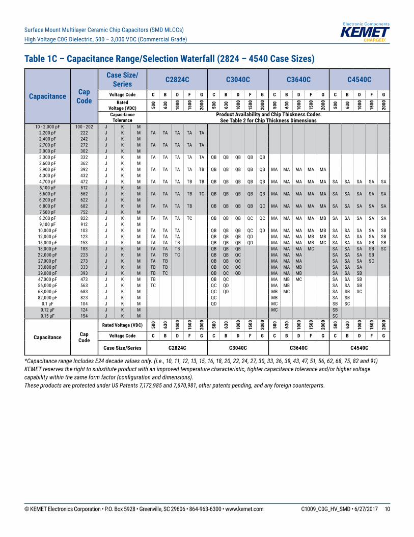
10 - 2,000 pF 100 - 202 J K M2,200 pF 222 J K M TA TA TA TA TA2,400 pF 242 J K M2,700 pF 272 J K M TA TA TA TA TA3,000 pF 302 J K M3,300 pF 332 J K M TA TA TA TA TA QB QB QB QB QB3,600 pF 362 J K M3,900 pF 392 J K M TA TA TA TA TB QB QB QB QB QB MA MA MA MA MA4,300 pF 432 J K M4,700 pF 472 J K M TA TA TA TB TB QB QB QB QB QB MA MA MA MA MA SA SA SA SA SA5,100 pF 512 J K M5,600 pF 562 J K M TA TA TA TB TC QB QB QB QB QB MA MA MA MA MA SA SA SA SA SA6,200 pF 622 J K M6,800 pF 682 J K M TA TA TA TB QB QB QB QB QC MA MA MA MA MA SA SA SA SA SA7,500 pF 752 J K M8,200 pF 822 J K M TA TA TA TC QB QB QB QC QC MA MA MA MA MB SA SA SA SA SA9,100 pF 912 J K M
10,000 pF 103 J K M TA TA TA QB QB QB QC QD MA MA MA MA MB SA SA SA SA SB12,000 pF 123 J K M TA TA TA QB QB QB QD MA MA MA MB MB SA SA SA SA SB15,000 pF 153 J K M TA TA TB QB QB QB QD MA MA MA MB MC SA SA SA SB SB18,000 pF 183 J K M TA TA TB QB QB QB MA MA MA MC SA SA SA SB SC22,000 pF 223 J K M TA TB TC QB QB QC MA MA MA SA SA SA SB27,000 pF 273 J K M TA TB QB QB QC MA MA MA SA SA SA SC33,000 pF 333 J K M TB TB QB QC QC MA MA MB SA SA SA39,000 pF 393 J K M TB TC QB QC QD MA MA MB SA SA SB47,000 pF 473 J K M TB QB QC MA MB MC SA SA SB56,000 pF 563 J K M TC QC QD MA MB SA SA SB68,000 pF 683 J K M QC QD MB MC SA SB SC82,000 pF 823 J K M QC MB SA SB
0.1 µF 104 J K M QD MC SB SC0.12 µF 124 J K M MC SB0.15 µF 154 J K M SC
Capacitance Cap Code
Rated Voltage (VDC) 500
630
1000
1500
2000
500
630
1000
1500
2000
500
630
1000
1500
2000
500
630
1000
1500
2000
Voltage Code C B D F G C B D F G C B D F G C B D F G
Case Size/Series C2824C C3040C C3640C C4540C
Table 1C – Capacitance Range/Selection Waterfall (2824 – 4540 Case Sizes)
*Capacitance range Includes E24 decade values only. (i.e., 10, 11, 12, 13, 15, 16, 18, 20, 22, 24, 27, 30, 33, 36, 39, 43, 47, 51, 56, 62, 68, 75, 82 and 91)KEMET reserves the right to substitute product with an improved temperature characteristic, tighter capacitance tolerance and/or higher voltage capability within the same form factor (configuration and dimensions).These products are protected under US Patents 7,172,985 and 7,670,981, other patents pending, and any foreign counterparts.

© KEMET Electronics Corporation • P.O. Box 5928 • Greenville, SC 29606 • 864-963-6300 • www.kemet.com C1009_C0G_HV_SMD • 6/27/2017 11
Surface Mount Multilayer Ceramic Chip Capacitors (SMD MLCCs)High Voltage C0G Dielectric, 500 – 3,000 VDC (Commercial Grade)
Table 2A – Chip Thickness/Tape & Reel Packaging Quantities
Thickness Code
Case Size
Thickness ± Range (mm)
Paper Quantity Plastic Quantity7" Reel 13" Reel 7" Reel 13" Reel
CG 0603 0.80 ± 0.10* 4,000 15,000 0 0DN 0805 0.78 ± 0.10* 4,000 15,000 0 0 DP 0805 0.90 ± 0.10* 4,000 15,000 0 0 DG 0805 1.25 ± 0.15 0 0 2,500 10,000 EB 1206 0.78 ± 0.10 4,000 10,000 4,000 10,000EC 1206 0.90 ± 0.10 0 0 4,000 10,000ED 1206 1.00 ± 0.10 0 0 2,500 10,000 EE 1206 1.10 ± 0.10 0 0 2,500 10,000EF 1206 1.20 ± 0.15 0 0 2,500 10,000EG 1206 1.60 ± 0.15 0 0 2,000 8,000 EH 1206 1.60 ± 0.20 0 0 2,000 8,000FE 1210 1.00 ± 0.10 0 0 2,500 10,000FF 1210 1.10 ± 0.10 0 0 2,500 10,000FG 1210 1.25 ± 0.15 0 0 2,500 10,000 FL 1210 1.40 ± 0.15 0 0 2,000 8,000FM 1210 1.70 ± 0.20 0 0 2,000 8,000FY 1210 2.00 ± 0.20 0 0 2,000 8,000 FK 1210 2.10 ± 0.20 0 0 2,000 8,000FS 1210 2.50 ± 0.30 0 0 1,000 4,000LA 1808 1.40 ± 0.15 0 0 1,000 4,000LB 1808 1.60 ± 0.15 0 0 1,000 4,000LC 1808 2.00 ± 0.15 0 0 1,000 4,000GH 1812 1.40 ± 0.15 0 0 1,000 4,000GK 1812 1.60 ± 0.20 0 0 1,000 4,000GM 1812 2.00 ± 0.20 0 0 500 2,000GO 1812 2.50 ± 0.20 0 0 500 2,000HE 1825 1.40 ± 0.15 0 0 1,000 4,000HG 1825 1.60 ± 0.20 0 0 1,000 4,000HJ 1825 2.00 ± 0.20 0 0 500 2,000HK 1825 2.50 ± 0.20 0 0 500 2,000JE 2220 1.40 ± 0.15 0 0 1,000 4,000JK 2220 1.60 ± 0.20 0 0 1,000 4,000JL 2220 2.00 ± 0.20 0 0 500 2,000JN 2220 2.50 ± 0.20 0 0 500 2,000KE 2225 1.40 ± 0.15 0 0 1,000 4,000KF 2225 1.60 ± 0.20 0 0 1,000 4,000KH 2225 2.00 ± 0.20 0 0 500 2,000KJ 2225 2.50 ± 0.20 0 0 500 2,000TA 2824 1.40 ± 0.15 0 0 750 2,500TB 2824 2.00 ± 0.20 0 0 300 2,000TC 2824 2.50 ± 0.20 0 0 300 2,000QB 3040 1.40 ± 0.15 0 0 500 1,650QC 3040 2.00 ± 0.20 0 0 500 1,650QD 3040 2.50 ± 0.20 0 0 350 1,400MA 3640 1.40 ± 0.15 0 0 250 1,550MB 3640 2.00 ± 0.20 0 0 250 1,550MC 3640 2.50 ± 0.20 0 0 250 1,550SA 4540 1.40 ± 0.15 0 0 200 1,500SB 4540 2.00 ± 0.20 0 0 200 1,500SC 4540 2.50 ± 0.20 0 0 200 1,500
Thickness Code
Case Size
Thickness ± Range (mm)
7" Reel 13" Reel 7" Reel 13" Reel
Paper Quantity Plastic Quantity
Package quantity based on finished chip thickness specifications.

© KEMET Electronics Corporation • P.O. Box 5928 • Greenville, SC 29606 • 864-963-6300 • www.kemet.com C1009_C0G_HV_SMD • 6/27/2017 12
Surface Mount Multilayer Ceramic Chip Capacitors (SMD MLCCs)High Voltage C0G Dielectric, 500 – 3,000 VDC (Commercial Grade)
Table 2B – Bulk Packaging Quantities
Packaging TypeLoose PackagingBulk Bag (default)
Packaging C-Spec1 N/A2
Case Size Packaging Quantities (pieces/unit packaging)EIA (in) Metric (mm) Minimum Maximum
0603 1608
1
50,0000805 20121206 32161210 32251808 4520
20,0001812 45321825 45642220 56502225 5664
1 The "Packaging C-Spec" is a 4 to 8 digit code which identifies the packaging type and/or product grade. When ordering, the proper code must be included in the 15th through 22nd character positions of the ordering code. See "Ordering Information" section of this document for further details. Commercial Grade product ordered without a packaging C-Spec will default to our standard "Bulk Bag" packaging. Contact KEMET if you require a bulk bag packaging option for Automotive Grade products.
2 A packaging C-Spec (see note 1 above) is not required for "Bulk Bag" packaging (excluding Anti-Static Bulk Bag and Automotive Grade products). The 15th through 22nd character positions of the ordering code should be left blank. All product ordered without a packaging C-Spec will default to our standard "Bulk Bag" packaging.

© KEMET Electronics Corporation • P.O. Box 5928 • Greenville, SC 29606 • 864-963-6300 • www.kemet.com C1009_C0G_HV_SMD • 6/27/2017 13
Surface Mount Multilayer Ceramic Chip Capacitors (SMD MLCCs)High Voltage C0G Dielectric, 500 – 3,000 VDC (Commercial Grade)
Table 3 – Chip Capacitor Land Pattern Design Recommendations per IPC–7351
EIA Size Code
Metric Size Code
Density Level A: Maximum (Most)
Land Protrusion (mm)
Density Level B: Median (Nominal)
Land Protrusion (mm)
Density Level C: Minimum (Least)
Land Protrusion (mm)C Y X V1 V2 C Y X V1 V2 C Y X V1 V2
0603 1608 0.90 1.15 1.10 4.00 2.10 0.80 0.95 1.00 3.10 1.50 0.60 0.75 0.90 2.40 1.20
0805 2012 1.00 1.35 1.55 4.40 2.60 0.90 1.15 1.45 3.50 2.00 0.75 0.95 1.35 2.80 1.70
1206 3216 1.60 1.35 1.90 5.60 2.90 1.50 1.15 1.80 4.70 2.30 1.40 0.95 1.70 4.00 2.00
1210 3225 1.60 1.35 2.80 5.65 3.80 1.50 1.15 2.70 4.70 3.20 1.40 0.95 2.60 4.00 2.90
1808 4520 2.30 1.75 2.30 7.40 3.30 2.20 1.55 2.20 6.50 2.70 2.10 1.35 2.10 5.80 2.40
1812 4532 2.15 1.60 3.60 6.90 4.60 2.05 1.40 3.50 6.00 4.00 1.95 1.20 3.40 5.30 3.70
1825 4564 2.15 1.60 6.90 6.90 7.90 2.05 1.40 6.80 6.00 7.30 1.95 1.20 6.70 5.30 7.00
2220 5650 2.75 1.70 5.50 8.20 6.50 2.65 1.50 5.40 7.30 5.90 2.55 1.30 5.30 6.60 5.60
2225 5664 2.70 1.70 6.90 8.10 7.90 2.60 1.50 6.80 7.20 7.30 2.50 1.30 6.70 6.50 7.00
2824 7260 3.45 1.70 6.60 9.60 7.60 3.35 1.50 6.50 8.70 7.00 3.25 1.30 6.40 8.00 6.70
3040 7610 3.70 1.70 10.70 10.10 11.70 3.60 1.50 10.60 9.20 11.10 3.50 1.30 10.50 8.50 10.80
3640 9210 4.45 1.70 10.70 11.60 11.70 4.35 1.50 10.60 10.70 11.10 4.25 1.30 10.50 10.00 10.80
4540 - 5.60 1.70 10.70 13.90 11.70 5.50 1.50 10.60 13.00 11.10 5.40 1.30 10.50 12.30 10.80
Density Level A: For low-density product applications. Recommended for wave solder applications and provides a wider process window for reflow solder processes. KEMET only recommends wave soldering of EIA 0603, 0805 and 1206 case sizes.Density Level B: For products with a moderate level of component density. Provides a robust solder attachment condition for reflow solder processes.Density Level C: For high component density product applications. Before adapting the minimum land pattern variations the user should perform qualification testing based on the conditions outlined in IPC Standard 7351 (IPC–7351).
Image below based on Density Level B for an EIA 1210 case size.
Y
C C
X X
V1
V2
Grid Placement Courtyard
Y
© KEMET Electronics Corporation • P.O. Box 5928 • Greenville, SC 29606 • 864-963-6300 • www.kemet.com C1009_C0G_HV_SMD • 6/27/2017 14
Surface Mount Multilayer Ceramic Chip Capacitors (SMD MLCCs)High Voltage C0G Dielectric, 500 – 3,000 VDC (Commercial Grade)
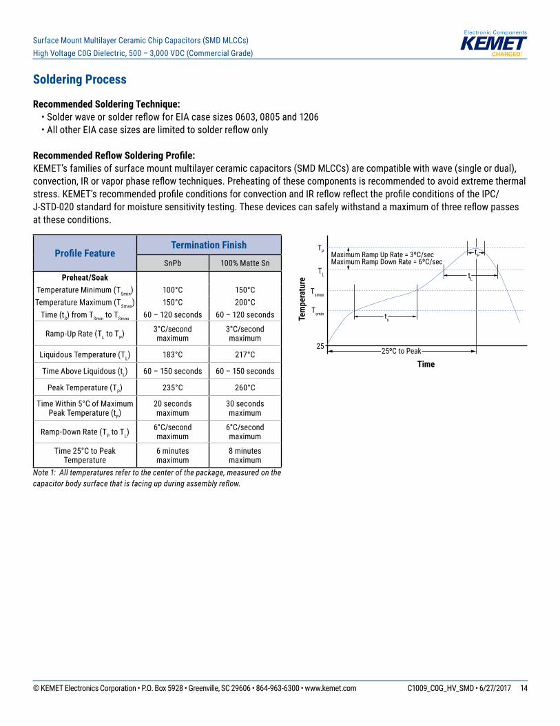
Soldering Process
Recommended Soldering Technique: • Solder wave or solder reflow for EIA case sizes 0603, 0805 and 1206 • All other EIA case sizes are limited to solder reflow only
Recommended Reflow Soldering Profile:KEMET’s families of surface mount multilayer ceramic capacitors (SMD MLCCs) are compatible with wave (single or dual), convection, IR or vapor phase reflow techniques. Preheating of these components is recommended to avoid extreme thermal stress. KEMET’s recommended profile conditions for convection and IR reflow reflect the profile conditions of the IPC/ J-STD-020 standard for moisture sensitivity testing. These devices can safely withstand a maximum of three reflow passes at these conditions.
Profile FeatureTermination Finish
SnPb 100% Matte Sn
Preheat/SoakTemperature Minimum (TSmin) 100°C 150°CTemperature Maximum (TSmax) 150°C 200°C
Time (tS) from TSmin to TSmax 60 – 120 seconds 60 – 120 seconds
Ramp-Up Rate (TL to TP) 3°C/second maximum
3°C/second maximum
Liquidous Temperature (TL) 183°C 217°C
Time Above Liquidous (tL) 60 – 150 seconds 60 – 150 seconds
Peak Temperature (TP) 235°C 260°C
Time Within 5°C of Maximum Peak Temperature (tP)
20 seconds maximum
30 seconds maximum
Ramp-Down Rate (TP to TL)6°C/second maximum
6°C/second maximum
Time 25°C to Peak Temperature
6 minutes maximum
8 minutes maximum
Note 1: All temperatures refer to the center of the package, measured on the capacitor body surface that is facing up during assembly reflow.
Time
Tem
pera
ture
Tsmin
25
Tsmax
TL
TP Maximum Ramp Up Rate = 3ºC/secMaximum Ramp Down Rate = 6ºC/sec
tP
tL
ts
25ºC to Peak

© KEMET Electronics Corporation • P.O. Box 5928 • Greenville, SC 29606 • 864-963-6300 • www.kemet.com C1009_C0G_HV_SMD • 6/27/2017 15
Surface Mount Multilayer Ceramic Chip Capacitors (SMD MLCCs)High Voltage C0G Dielectric, 500 – 3,000 VDC (Commercial Grade)
Table 4 – Performance & Reliability: Test Methods and Conditions
Stress Reference Test or Inspection MethodTerminal Strength JIS–C–6429 Appendix 1, Note: Force of 1.8 kg for 60 seconds.
Board Flex JIS–C–6429 Appendix 2, Note: Standard termination system – 2.0 mm (minimum) for all except 3 mm for C0G. Flexible termination system – 3.0 mm (minimum).
Solderability J–STD–002
Magnification 50 X. Conditions:
a) Method B, 4 hours at 155°C, dry heat at 235°C
b) Method B at 215°C category 3
c) Method D, category 3 at 260°C
Temperature Cycling JESD22 Method JA–104 1,000 cycles (−55°C to +125°C). Measurement at 24 hours +/−4 hours after test conclusion.
Biased Humidity MIL–STD–202 Method 103
Load Humidity: 1,000 hours 85°C/85% RH and 200 VDC maximum. Add 100 K ohm resistor. Measurement at 24 hours +/−4 hours after test conclusion.Low Volt Humidity: 1,000 hours 85°C/85% RH and 1.5 V. Add 100 K ohm resistor. Measurement at 24 hours +/−4 hours after test conclusion.
Moisture Resistance MIL–STD–202 Method 106
t = 24 hours/cycle. Steps 7a and 7b not required. Measurement at 24 hours +/−4 hours after test conclusion.
Thermal Shock MIL–STD–202 Method 107
−55°C/+125°C. Note: Number of cycles required – 300. Maximum transfer time – 20 seconds. Dwell time – 15 minutes. Air – Air.
High Temperature Life MIL–STD–202 Method 108 1,000 hours at 125°C (85°C for X5R, Z5U and Y5V) with 1.2 X rated voltage applied.
Storage Life MIL–STD–202 Method 108 150°C, 0 VDC for 1,000 hours.
Vibration MIL–STD–202 Method 204
5 g's for 20 min., 12 cycles each of 3 orientations. Note: Use 8" X 5" PCB 0.031" thick 7 secure points on one long side and 2 secure points at corners of opposite sides. Parts mounted within 2" from any secure point. Test from 10 – 2,000 Hz
Mechanical Shock MIL–STD–202 Method 213 Figure 1 of Method 213, Condition F.
Resistance to Solvents MIL–STD–202 Method 215 Add aqueous wash chemical, OKEM Clean or equivalent.
Storage and Handling
Ceramic chip capacitors should be stored in normal working environments. While the chips themselves are quite robust in other environments, solderability will be degraded by exposure to high temperatures, high humidity, corrosive atmospheres, and long term storage. In addition, packaging materials will be degraded by high temperature–reels may soften or warp and tape peel force may increase. KEMET recommends that maximum storage temperature not exceed 40ºC and maximum storage humidity not exceed 70% relative humidity. Temperature fluctuations should be minimized to avoid condensation on the parts and atmospheres should be free of chlorine and sulfur bearing compounds. For optimized solderability chip stock should be used promptly, preferably within 1.5 years of receipt.

© KEMET Electronics Corporation • P.O. Box 5928 • Greenville, SC 29606 • 864-963-6300 • www.kemet.com C1009_C0G_HV_SMD • 6/27/2017 16
Surface Mount Multilayer Ceramic Chip Capacitors (SMD MLCCs)High Voltage C0G Dielectric, 500 – 3,000 VDC (Commercial Grade)
Construction
Detailed Cross Section
Barrier Layer(Ni)
Inner Electrodes(Ni)
Barrier Layer(Ni)
Inner Electrodes(Ni)
Dielectric Material(CaZrO3)Dielectric Material
(CaZrO3)
Termination Finish(100% Matte Sn / SnPb - 5% Pb min)
Termination Finish(100% Matte Sn / SnPb - 5% Pb min)
End Termination/External Electrode
(Cu)
End Termination/External Electrode
(Cu)
Capacitor Marking (Optional):
Laser marking option is not available on:
• C0G, Ultra Stable X8R and Y5V dielectric devices • EIA 0402 case size devices • EIA 0603 case size devices with Flexible Termination option.• KPS Commercial and Automotive grade stacked devices.
These capacitors are supplied unmarked only.

© KEMET Electronics Corporation • P.O. Box 5928 • Greenville, SC 29606 • 864-963-6300 • www.kemet.com C1009_C0G_HV_SMD • 6/27/2017 17
Surface Mount Multilayer Ceramic Chip Capacitors (SMD MLCCs)High Voltage C0G Dielectric, 500 – 3,000 VDC (Commercial Grade)
Tape & Reel Packaging InformationKEMET offers multilayer ceramic chip capacitors packaged in 8, 12, 16 and 24 mm tape on 7" and 13" reels in accordance with EIA Standard 481. This packaging system is compatible with all tape-fed automatic pick and place systems. See Table 2 for details on reeling quantities for commercial chips.
8 mm, 12 mmor 16 mm Carrier Tape 178 mm (7.00")
or330 mm (13.00")
Anti-Static Reel
Embossed Plastic* or Punched Paper Carrier.
Embossment or Punched Cavity
Anti-Static Cover Tape(.10 mm (.004") Maximum Thickness)
Chip and KPS Orientation in Pocket(except 1825 Commercial, and 1825 and 2225 Military)
*EIA 01005, 0201, 0402 and 0603 case sizes available on punched paper carrier only.
KEMET®
Bar Code Label
Sprocket Holes
Table 5 – Carrier Tape Confi guration, Embossed Plastic & Punched Paper (mm)
EIA Case SizeTape Size (W)*
Embossed Plastic Punched Paper7" Reel 13" Reel 7" Reel 13" Reel
Pitch (P1)* Pitch (P1)*
01005 – 0402 8 2 2
0603 8 2/4 2/4
0805 8 4 4 4 4
1206 – 1210 8 4 4 4 4
1805 – 1808 12 4 4
≥ 1812 12 8 8
2824 16 12 12
3040 – 4540 24 16 16
KPS 1210 12 8 8
KPS 1812 & 2220 16 12 12
Array 0508 & 0612 8 4 4
*Refer to Figures 1 & 2 for W and P1 carrier tape reference locations.*Refer to Tables 6 & 7 for tolerance specifi cations.
New 2 mm Pitch Reel Options*
PackagingOrdering Code
(C-Spec)Packaging Type/Options
C-3190 Automotive grade 7" reel unmarkedC-3191 Automotive grade 13" reel unmarkedC-7081 Commercial grade 7" reel unmarkedC-7082 Commercial grade 13" reel unmarked
* 2 mm pitch reel only available for 0603 EIA case size. 2 mm pitch reel for 0805 EIA case size under development.
Benefi ts of Changing from 4 mm to 2 mm Pitching Spacing• Lower placement costs• Double the parts on each reel results in fewer reel
changes and increased effi ciency• Fewer reels result in lower packaging, shipping and
storage costs, reducing waste

© KEMET Electronics Corporation • P.O. Box 5928 • Greenville, SC 29606 • 864-963-6300 • www.kemet.com C1009_C0G_HV_SMD • 6/27/2017 18
Surface Mount Multilayer Ceramic Chip Capacitors (SMD MLCCs)High Voltage C0G Dielectric, 500 – 3,000 VDC (Commercial Grade)
Figure 1 – Embossed (Plastic) Carrier Tape Dimensions
PoT
F
W
Center Lines of Cavity
Ao
Bo
User Direction of Unreeling
Cover Tape
Ko
B 1 is for tape feeder reference only, including draft concentric about Bo.
T 2
ØD 1
ØDo
B 1
S 1
T1
E 1
E 2
P 1
P 2
EmbossmentFor cavity size,see Note 1 Table 4
[10 pitches cumulativetolerance on tape ± 0.2 mm]
Table 6 – Embossed (Plastic) Carrier Tape DimensionsMetric will govern
Constant Dimensions — Millimeters (Inches)
Tape Size D0 E1 P0 P2 R Reference
Note 2S1 Minimum
Note 3T
MaximumT1
Maximum
8 mm
1.5+0.10/−0.0(0.059+0.004/−0.0)
1.75±0.10(0.069±0.004)
4.0±0.10(0.157±0.004)
2.0±0.05(0.079±0.002)
25.0(0.984)
0.600(0.024)
0.600(0.024)
0.100(0.004)12 mm
30(1.181)
16 mm
24 mm 1.5+0.10/−0.0(0.059+0.004/−0.0)
1.75±0.10(0.069±0.004)
4.0±0.10(0.157±0.004)
2.0±0.10(0.078±0.003)
30(1.181)
5(0.196)
0.250(0.009)
0.350(0.013)
Variable Dimensions — Millimeters (Inches)
Tape Size Pitch E2Minimum F P1
T2Maximum
WMaximum A0,B0 & K0
8 mm Single (4 mm) 6.25(0.246)
3.5±0.05(0.138±0.002)
4.0±0.10(0.157±0.004)
2.5(0.098)
8.3(0.327)
Note 512 mm Single (4 mm) &
Double (8 mm)10.25
(0.404)5.5±0.05
(0.217±0.002)8.0±0.10
(0.315±0.004)4.6
(0.181)12.3
(0.484)
16 mm Triple (12 mm) 14.25(0.561)
7.5±0.05(0.138±0.002)
12.0±0.10(0.157±0.004)
4.6(0.181)
16.3(0.642)
24 mm 16 mm 22.25(0.875)
11.5±0.10(0.452±0.003)
16.0±0.10(0.629±0.004)
3(0.118)
24.3(0.956)
1. The embossment hole location shall be measured from the sprocket hole controlling the location of the embossment. Dimensions of embossment location and hole location shall be applied independent of each other.
2. The tape with or without components shall pass around R without damage (see Figure 6).3. If S1 < 1.0 mm, there may not be enough area for cover tape to be properly applied (see EIA Standard 481 paragraph 4.3 section b).4. B1 dimension is a reference dimension for tape feeder clearance only.5. The cavity defi ned by A0, B0 and K0 shall surround the component with suffi cient clearance that: (a) the component does not protrude above the top surface of the carrier tape. (b) the component can be removed from the cavity in a vertical direction without mechanical restriction, after the top cover tape has been removed. (c) rotation of the component is limited to 20° maximum for 8 and 12 mm tapes and 10° maximum for 16 mm tapes (see Figure 3). (d) lateral movement of the component is restricted to 0.5 mm maximum for 8 and 12 mm wide tape and to 1.0 mm maximum for 16 mm tape (see
Figure 4). (e) for KPS Series product, A0 and B0 are measured on a plane 0.3 mm above the bottom of the pocket. (f) see Addendum in EIA Standard 481 for standards relating to more precise taping requirements.

© KEMET Electronics Corporation • P.O. Box 5928 • Greenville, SC 29606 • 864-963-6300 • www.kemet.com C1009_C0G_HV_SMD • 6/27/2017 19
Surface Mount Multilayer Ceramic Chip Capacitors (SMD MLCCs)High Voltage C0G Dielectric, 500 – 3,000 VDC (Commercial Grade)
Figure 2 – Punched (Paper) Carrier Tape Dimensions
User Direction of Unreeling
Top Cover Tape
T
Center Lines of Cavity
P1
ØDo Po E1
F
E2W
G
A0
B0
Cavity Size,SeeNote 1, Table 7
Bottom Cover Tape
T1
T1
Bottom Cover Tape
[10 pitches cumulativetolerance on tape ± 0.2 mm]
Table 7 – Punched (Paper) Carrier Tape Dimensions Metric will govern
Constant Dimensions — Millimeters (Inches)Tape Size D0 E1 P0 P2 T1 Maximum G Minimum R Reference
Note 2
8 mm 1.5+0.10/−0.0(0.059+0.004/−0.0)
1.75±0.10(0.069±0.004)
4.0±0.10(0.157±0.004)
2.0±0.05(0.079±0.002)
0.10(0.004)
Maximum0.75
(0.030) 2
(0.984)
Variable Dimensions — Millimeters (Inches)Tape Size Pitch E2 Minimum F P1 T Maximum W Maximum A0 B0
8 mm Half (2 mm) 6.25(0.246)
3.5±0.05(0.138±0.002)
2.0±0.05(0.079±0.002) 1.1
(0.098)
8.3(0.327) Note 1
8 mm Single (4 mm) 4.0±0.10(0.157±0.004)
8.3(0.327)
1. The cavity defi ned by A0, B0 and T shall surround the component with suffi cient clearance that: a) the component does not protrude beyond either surface of the carrier tape. b) the component can be removed from the cavity in a vertical direction without mechanical restriction, after the top cover tape has been removed. c) rotation of the component is limited to 20° maximum (see Figure 3). d) lateral movement of the component is restricted to 0.5 mm maximum (see Figure 4). e) see Addendum in EIA Standard 481 for standards relating to more precise taping requirements.2. The tape with or without components shall pass around R without damage (see Figure 6).

© KEMET Electronics Corporation • P.O. Box 5928 • Greenville, SC 29606 • 864-963-6300 • www.kemet.com C1009_C0G_HV_SMD • 6/27/2017 20
Surface Mount Multilayer Ceramic Chip Capacitors (SMD MLCCs)High Voltage C0G Dielectric, 500 – 3,000 VDC (Commercial Grade)
Packaging Information Performance Notes
1. Cover Tape Break Force: 1.0 Kg minimum.2. Cover Tape Peel Strength: The total peel strength of the cover tape from the carrier tape shall be:
Tape Width Peel Strength8 mm 0.1 to 1.0 Newton (10 to 100 gf)
12 and 16 mm 0.1 to 1.3 Newton (10 to 130 gf)
24 mm 0.1 to 1.6 Newton (10 to 160 gf)
The direction of the pull shall be opposite the direction of the carrier tape travel. The pull angle of the carrier tape shall be 165° to 180° from the plane of the carrier tape. During peeling, the carrier and/or cover tape shall be pulled at a velocity of 300±10 mm/minute.3. Labeling: Bar code labeling (standard or custom) shall be on the side of the reel opposite the sprocket holes. Refer to EIA Standards 556 and 624.
Figure 3 – Maximum Component Rotation
Ao
Bo
°T
°s
Maximum Component RotationTop View
Maximum Component RotationSide View
Tape MaximumWidth (mm) Rotation ( °
T)8,12 20 16 – 200 10 Tape Maximum
Width (mm) Rotation ( °S)
8,12 20 16 – 56 1072 – 200 5
Typical Pocket Centerline
Typical Component Centerline
Figure 4 – Maximum Lateral Movement
0.5 mm maximum0.5 mm maximum
8 mm & 12 mm Tape
1.0 mm maximum1.0 mm maximum
16 mm Tape
Figure 5 – Bending Radius
RRBending
Radius
EmbossedCarrier
PunchedCarrier

© KEMET Electronics Corporation • P.O. Box 5928 • Greenville, SC 29606 • 864-963-6300 • www.kemet.com C1009_C0G_HV_SMD • 6/27/2017 21
Surface Mount Multilayer Ceramic Chip Capacitors (SMD MLCCs)High Voltage C0G Dielectric, 500 – 3,000 VDC (Commercial Grade)
Figure 6 – Reel Dimensions
A D (See Note)
Full Radius,See Note
B (see Note)
Access Hole atSlot Location(Ø 40 mm minimum)
If present,tape slot in corefor tape start:2.5 mm minimum width x10.0 mm minimum depth
W3 (Includes flange distortion at outer edge)
W2 (Measured at hub)
W1 (Measured at hub)
C(Arbor holediameter)
Note: Drive spokes optional; if used, dimensions B and D shall apply.
N
Table 8 – Reel DimensionsMetric will govern
Constant Dimensions — Millimeters (Inches) Tape Size A B Minimum C D Minimum
8 mm178±0.20
(7.008±0.008) or
330±0.20(13.000±0.008)
1.5 (0.059)
13.0+0.5/−0.2 (0.521+0.02/−0.008)
20.2 (0.795)12 mm
16 mm
24 mm 1.2(0.047)
13.0 + −0.2 (0.521 + −0.008)
21(0.826)
Variable Dimensions — Millimeters (Inches) Tape Size N Minimum W1 W2 Maximum W3
8 mm
50 (1.969)
8.4+1.5/−0.0(0.331+0.059/−0.0)
14.4 (0.567)
Shall accommodate tape width without interference
12 mm 12.4+2.0/−0.0(0.488+0.078/−0.0)
18.4 (0.724)
16 mm 16.4+2.0/−0.0(0.646+0.078/−0.0)
22.4 (0.882)
24 mm 25+1.0/−0.0(0.984+0.039/−0.0)
27.4+1.0/−1.0(1.078+0.039/−0.039)

© KEMET Electronics Corporation • P.O. Box 5928 • Greenville, SC 29606 • 864-963-6300 • www.kemet.com C1009_C0G_HV_SMD • 6/27/2017 22
Surface Mount Multilayer Ceramic Chip Capacitors (SMD MLCCs)High Voltage C0G Dielectric, 500 – 3,000 VDC (Commercial Grade)
Figure 7 – Tape Leader & Trailer Dimensions
Trailer160 mm Minimum
Carrier Tape
END STARTRound Sprocket Holes
Elongated Sprocket Holes(32 mm tape and wider)
Top Cover Tape
Top Cover Tape
Punched Carrier8 mm & 12 mm only
Embossed Carrier
Components
100 mm Minimum Leader
400 mm Minimum
Figure 8 – Maximum Camber
Carrier TapeRound Sprocket Holes
2 mm Maximum, either direction for 8 mm wide tape
Straight Edge
250 mm
Elongated Sprocket Holes(32 mm & wider tapes)

© KEMET Electronics Corporation • P.O. Box 5928 • Greenville, SC 29606 • 864-963-6300 • www.kemet.com C1009_C0G_HV_SMD • 6/27/2017 23
Surface Mount Multilayer Ceramic Chip Capacitors (SMD MLCCs)High Voltage C0G Dielectric, 500 – 3,000 VDC (Commercial Grade)
KEMET Electronics Corporation Sales Offi ces
For a complete list of our global sales offi ces, please visit www.kemet.com/sales.
DisclaimerAll product specifi cations, statements, information and data (collectively, the “Information”) in this datasheet are subject to change. The customer is responsible for checking and verifying the extent to which the Information contained in this publication is applicable to an order at the time the order is placed.
All Information given herein is believed to be accurate and reliable, but it is presented without guarantee, warranty, or responsibility of any kind, expressed or implied.
Statements of suitability for certain applications are based on KEMET Electronics Corporation’s (“KEMET”) knowledge of typical operating conditions for such applications, but are not intended to constitute – and KEMET specifi cally disclaims – any warranty concerning suitability for a specifi c customer application or use. The Information is intended for use only by customers who have the requisite experience and capability to determine the correct products for their application. Any technical advice inferred from this Information or otherwise provided by KEMET with reference to the use of KEMET’s products is given gratis, and KEMET assumes no obligation or liability for the advice given or results obtained.
Although KEMET designs and manufactures its products to the most stringent quality and safety standards, given the current state of the art, isolated component failures may still occur. Accordingly, customer applications which require a high degree of reliability or safety should employ suitable designs or other safeguards (such as installation of protective circuitry or redundancies) in order to ensure that the failure of an electrical component does not result in a risk of personal injury or property damage.
Although all product–related warnings, cautions and notes must be observed, the customer should not assume that all safety measures are indicted or that other measures may not be required.
KEMET is a registered trademark of KEMET Electronics Corporation.
Related Documents