HAL Id: hal-01795072 https://hal.archives-ouvertes.fr/hal-01795072 Submitted on 18 May 2018 HAL is a multi-disciplinary open access archive for the deposit and dissemination of sci- entific research documents, whether they are pub- lished or not. The documents may come from teaching and research institutions in France or abroad, or from public or private research centers. L’archive ouverte pluridisciplinaire HAL, est destinée au dépôt et à la diffusion de documents scientifiques de niveau recherche, publiés ou non, émanant des établissements d’enseignement et de recherche français ou étrangers, des laboratoires publics ou privés. Surface morphology in tungsten and RAFM steel exposed to helium plasma in PSI-2 Ryuichi Sakamoto, Elodie Bernard, Arkadi Kreter, Céline Martin, Bernard Pegourié, Grégory Pieters, Bernard Rousseau, Christian Grisolia, Naoaki Yoshida To cite this version: Ryuichi Sakamoto, Elodie Bernard, Arkadi Kreter, Céline Martin, Bernard Pegourié, et al.. Surface morphology in tungsten and RAFM steel exposed to helium plasma in PSI-2. Physica Scripta, IOP Publishing, 2017, T170, pp.014062. 10.1088/1402-4896/aa93a2. hal-01795072

Welcome message from author
This document is posted to help you gain knowledge. Please leave a comment to let me know what you think about it! Share it to your friends and learn new things together.
Transcript

HAL Id: hal-01795072https://hal.archives-ouvertes.fr/hal-01795072
Submitted on 18 May 2018
HAL is a multi-disciplinary open accessarchive for the deposit and dissemination of sci-entific research documents, whether they are pub-lished or not. The documents may come fromteaching and research institutions in France orabroad, or from public or private research centers.
L’archive ouverte pluridisciplinaire HAL, estdestinée au dépôt et à la diffusion de documentsscientifiques de niveau recherche, publiés ou non,émanant des établissements d’enseignement et derecherche français ou étrangers, des laboratoirespublics ou privés.
Surface morphology in tungsten and RAFM steelexposed to helium plasma in PSI-2
Ryuichi Sakamoto, Elodie Bernard, Arkadi Kreter, Céline Martin, BernardPegourié, Grégory Pieters, Bernard Rousseau, Christian Grisolia, Naoaki
Yoshida
To cite this version:Ryuichi Sakamoto, Elodie Bernard, Arkadi Kreter, Céline Martin, Bernard Pegourié, et al.. Surfacemorphology in tungsten and RAFM steel exposed to helium plasma in PSI-2. Physica Scripta, IOPPublishing, 2017, T170, pp.014062. �10.1088/1402-4896/aa93a2�. �hal-01795072�

Surface morphology in tungsten and RAFM steel
exposed to helium plasma in PSI-2
Ryuichi Sakamoto1,7§, Elodie Bernard2, Arkadi Kreter3,
Celine Martin4, Bernard Pegourie2, Gregory Pieters5,
Bernard Rousseau5, Christian Grisolia2,8 and Naoaki Yoshida6
1 NINS, National Institute for Fusion Science, Toki, Gifu 509-5292, Japan2 CEA, IRFM, F-13108 Saint-Paul-lez-Durance, France3 Forschungszentrum Julich GmbH, Institut fur Energie- und Klimaforschung -
Plasmaphysik, 52425 Julich, Germany4 Universite Aix-Marseille, PIIM, 13397 Marseille, France5 CEA Saclay, SCBM, F-91191 Gif-sur-Yvette, France6 Kyushu University, RIAM, Kasuga, Fukuoka 816-8580, Japan7 The Graduate University for Advanced Studies, Toki, Gifu 509-5292, Japan8 National Research Nuclear University“MEPhI”, Moscow, 115409 Russian
Federation
Abstract. Impact of the helium plasma exposure on the surface modification
in tungsten and RAFM (Reduced Activation Ferritic/Martensitic) steel have been
investigated on the linear plasma device PSI-2 assuming the condition of DEMO first
wall. In tungsten, a nanoscale undulating surface structure, which has a periodic
arrangement, is formed under low temperature conditions below fuzz nanostructure
formation threshold ∼ 1000 K. Interval and direction of the undulation shows
dependence on the crystal orientation. A large variation in surface level up to 200 nm
has been observed among grains at a fluence of 3 × 1026 He/m2 showing dependence
of the surface erosion rate on the crystal orientation. The {100} plane in which
the undulating surface structure is not formed shows the highest erosion rate. This
significant erosion is due to the multistage sputtering through impurity. In RAFM
steel, sponge-like nanostructure is developed and it grows with increasing helium
fluence beyond 1 µm. In the sponge-like nanostructure, a composition change from
the base material is observed in which the tungsten ratio increases while the iron ratio
decreases showing differences in sputtering ratio depending on the atomic mass.
Submitted to: Phys. Scr.
§ Corresponding author: [email protected]

Surface morphology in tungsten and RAFM steel exposed to helium plasma in PSI-2 2
1. Introduction
In a demonstration fusion plant (DEMO), tungsten is a primary candidate for plasma
facing materials, which are exposed not only to hydrogen isotope fuel but also to
helium ash from the burning plasma, due to its excellent high temperature properties,
high sputtering threshold energy, low hydrogen retention and acceptable induced
radioactivity [1]. Assuming tungsten usa conditions at the first wall, which is exposed
to the radiation and charge exchange particles from the main plasma and scrape-
off-layer (SOL) plasma, the total incident particle flux is estimated as 1021 − 1022
particles/m2/s, and several % of helium will be part of the incident flux. From the
viewpoint of protection of the in vessel components from the above mentioned heat
and particle load, a robust first wall will be required. At the same time, from the
viewpoint of maximization of the tritium breeding ratio in the blanket, minimization
of neutron attenuation will be required by reducing the thickness of the tungsten first
wall. Consequently, only a thin tungsten coating layer (sub mm to few mm) on the
blanket surface is envisaged as the first wall to protect the blanket from the incident
heat and particles [2,3]. The lifetime of the blanket, therefore, will be affected by erosion
characteristics of the tungsten first wall. Since Reduced Activation Ferritic/Martensitic
(RAFM) steels are presently considered as a primary candidates for structural materials
of the blanket in a demonstration fusion plant, tolerance of RAFM steel to the plasma
exposure is another issue for the unexpected situation in which the tungsten first wall
is removed accidentally.
Over the past decade a considerable number of studies have been made on tungsten
as a plasma facing material from both experimental and theoretical aspect [4, 5].
These results show strong impact of the helium exposure on surface modifications of
tungsten even at low incident energy below the displacement damage threshold. These
results imply the importance of helium effects on tungsten as a plasma facing material.
Considering the first wall structure, the operational temperature should be limited by
the maximum allowable temperature of the blanket, that is ∼ 823 K in the case in
which the RAFM steel is chosen as a blanket structure material [6]. This temperature
is significantly below the lower threshold of the fuzz nanostructure formation, that
is, ∼ 1000 K [7]. Although a large number of studies have been conducted on the fuzz
nanostructure [7–10], little attention has been given to such low temperature ranges [11].
This motivates us to investigate helium exposure at relatively low temperature.
In this study, we have investigated helium exposure effect on tungsten and RAFM
steel at the operational temperature of a demonstration fusion plant (∼ 800 K) using the
linear plasma device PSI-2. The samples exposed to helium plasma have been analyzed
from the viewpoint of micro-structural morphology of the material surface.
Surface morphology in tungsten and RAFM steel exposed to helium plasma in PSI-2 3
2. Experimental setup
For tungsten, high-purity tungsten (> 99.995 %, Toho Kinzoku Co. Ltd.) samples were
mechanically polished and then annealed at 1773 K under vacuum conditions for 2 h
in order to obtain a several 10 µm monocrystal grain for the surface analysis, releasing
rolling stress and enhancing recrystallization. For RAFM steel, JLF-1 (Japanese Low
activation Ferritic steel) JOYO-II HEAT, which compositions are Fe, 9.00 wt% Cr,
1.98 wt% W, 0.49 wt% Mn, 0.20 wt% V, 0.083 wt% Ta, 0.09 wt% C, were mechanically
polished and then finished by electrolytic polishing for removing a mechanical processing
affected layer. The dimensions of both tungsten and RAFM steel samples are 7 mm×7
mm square and 0.3 mm thick.
Helium exposure experiments were carried out using linear plasma device PSI-2 [12].
Typical incident helium energy was mono-energetic 75 eV. This incident helium energy
is slightly lower than the threshold energy of the sputtering yield for tungsten [13, 14],
while it is above the threshold energy for RAFM. The sample temperature was controlled
to around 800 K by a combination of forced water cooling and electric heaters, taking
into account the heat flux from the plasma. The sample temperature was measured
by an infrared (IR) camera and cross-checked with a thermocouple installed under the
sample. Two tungsten and two RAFM steel samples, four samples in total, were fixed at
the sample-holder by a bolted molybdenum mask plate and exposed to helium plasma
at a flux of ∼ 1.6× 10²² He/m2/s.
The helium exposure effects on tungsten and RAFM steel have been investigated
from the viewpoint of micro-structural morphology using the multi surface analysis
techniques, including transmission and scanning electron microscopy (TEM, STEM and
SEM), energy dispersive X-ray spectrometry (EDS), focused ion beam (FIB), electron
backscatter diffraction (EBSD), and confocal laser microscopy (CLM).
3. Helium exposure impact on surface modification
3.1. Tungsten
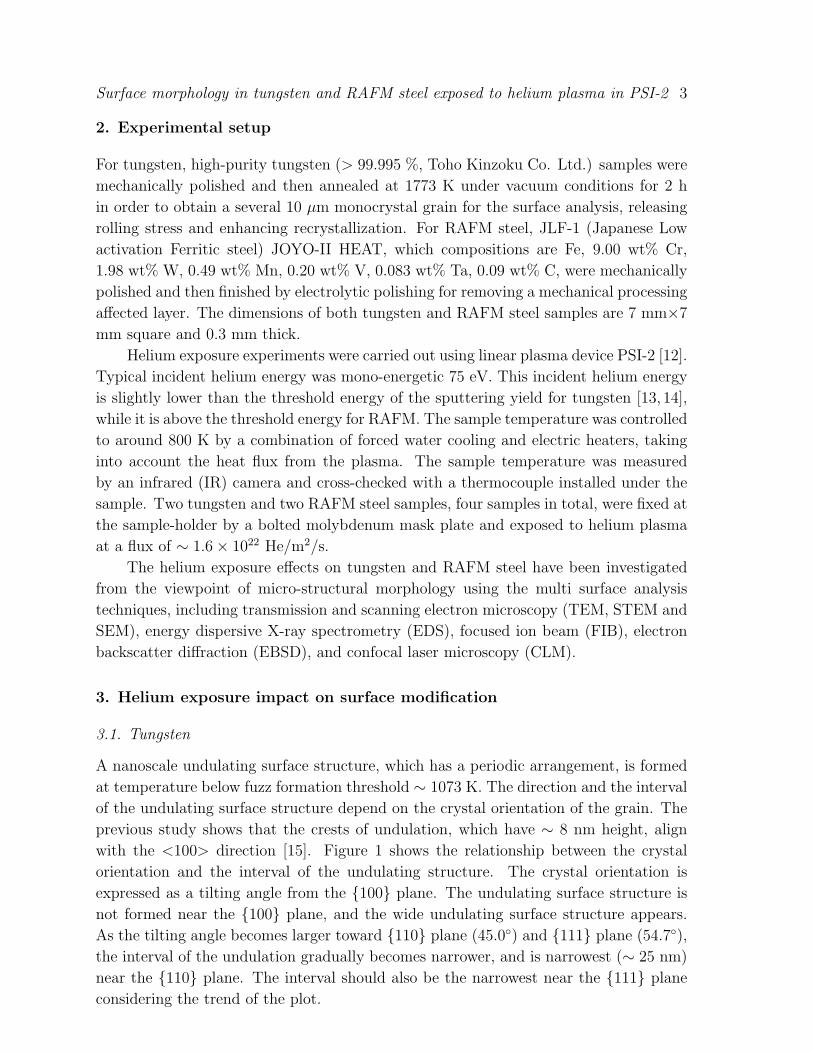
A nanoscale undulating surface structure, which has a periodic arrangement, is formed
at temperature below fuzz formation threshold ∼ 1073 K. The direction and the interval
of the undulating surface structure depend on the crystal orientation of the grain. The
previous study shows that the crests of undulation, which have ∼ 8 nm height, align
with the <100> direction [15]. Figure 1 shows the relationship between the crystal
orientation and the interval of the undulating structure. The crystal orientation is
expressed as a tilting angle from the {100} plane. The undulating surface structure is
not formed near the {100} plane, and the wide undulating surface structure appears.
As the tilting angle becomes larger toward {110} plane (45.0◦) and {111} plane (54.7◦),
the interval of the undulation gradually becomes narrower, and is narrowest (∼ 25 nm)
near the {110} plane. The interval should also be the narrowest near the {111} plane
considering the trend of the plot.

Surface morphology in tungsten and RAFM steel exposed to helium plasma in PSI-2 4
Figure 2 (a) shows typical SEM image of the grain boundary between grains, which
have surface near the {100} and the {110} plane, at a fluence of 3 × 1026 He/m2.
In addition to the undulating surface structure, which is developed in the right hand
side grain, holes (small black dot contrast) and flakes (small white dot contrast) which
originate from the aggregation of the helium bubbles are observed all over the surface,
showing the possibility of nano-dust generation. Hole and flake, which are developed
from the aggregation of the helium bubbles, are shown in Figure 2 (b).
The undulating surface structure begins to form at a fluence above 1024 He/m2, and
its development is almost saturated at a fluence above 1025 He/m2. On the other hand,
surface erosion should continue to progress during exposure because large variations in
surface level among grains have been observed by the SEM images as shown in Figure
3. The black band at the center of the SEM image is carbon deposit for the FIB process
to make a cross-sectional sample. From the cross-sectional observation at the grain
boundary (Figure 3 (b)), the maximum difference in surface level reaches to 140 nm.
This fact shows that the surface erosion rate varies depending on the crystal orientation
of the grain.
Figure 4 shows histograms of the relative surface level measured by the CLM in a
region of 129 µm square with 0.129 µm spatial resolution. In the case of 1×1025 He/m2,
the width of the histogram is within 50 nm. This width is the same width as the pristine
sample before the plasma exposure. Therefore, the erosion is not obvious at fluence of
1 × 1025 He/m2, and it can be said that the ambiguity of the measurement, which
includes the initial distortion of the sample and measurement error, is approximately
50 nm. The histogram width becomes wider with increasing helium fluence, 120 nm at
1 × 1026 He/m2 and 200 nm at 3 × 1026 He/m2, showing an increase of erosion. There
are three obvious peaks in the histogram as shown by vertical arrows and plotted in
Figure 4. This peak may indicate three groups of specific crystal orientations. Since
the peak height can be affected by not only the crystal orientation dependence of the
erosion but also the initial distribution of the crystal orientation, additional information
on the crystal orientation is required for a full understanding.
In order to investigate a crystal orientation dependence of the erosion rate, crystal
orientation mapping by the EBSD analysis and surface level mapping by the CLM
analysis have been compared. Figure 5 (a) shows SEM image, crystal orientation map
and surface level map of the identical area. The distribution of crystal orientation and
relative grain size within the area of interest are indicated in the orientation triangle
(Figure 5 (b)). Moreover, the distribution of crystal orientation is projected against
the surface tilting angle from the {100} plane in Figure 5 (c). The {100} and {111}
planes correspond to the 45.0◦ and 54.7◦ in the surface tilting angle. As is obvious from
the crystal orientation map which is dominated by red color, the crystal orientation is
broadly concentrated near the {100} plane (distribution peak at 10◦ − 15◦) and mainly
spreads to the {111} plane. This may be the texture due to the recrystallization process
at the sample preparation. Nevertheless, there is a green color grain which shows
the {110} plane. Therefore, whole orientation grains are contained within the area

Surface morphology in tungsten and RAFM steel exposed to helium plasma in PSI-2 5
of interest. The area of the circles in Figure 5 (b) relatively corresponds with the grain
size (area), which is distributed between 5 - 1500 µm2. There is no clear dependence of
the grain size on crystal orientation.
The relative surface level, which is measured by the CLM, is plotted against the
surface tilting angle from the {100} plane in Figure 6. At the {100} plane, where
the nanoscale undulating surface structure cannot be formed, the surface level is the
minimum level which shows that the surface erosion reached the maximum. And the
relative surface level is increased proportionally as the tilting angle increases. At the
{110} and the {111} planes where the nanoscale undulating surface structure is formed,
the surface level is relatively high, showing that the erosion rate is slower than the {100}
plane. It became clear that the large difference in surface level up to 200 nm is formed at
a fluence of 3× 1026 He/m2 due to the crystal orientation impact on the surface erosion
rate. The highest erosion yield for the grains with orientation close to the {100} is also
observed in the Ar or Ne seeding deuterium plasma exposure experiments [16]. On the
other hand, theoretical study [14] predicted that the {110} plane have a significantly
higher sputtering yield than the {100} plane or the {111} plane, because the {110}
plane is the most closely-packed of the three, and hence most likely to produce a direct
helium−tungsten collision.
Despite the fact that there is a large erosion up to 200 nm at a fluence of 3× 1026
He/m2, the undulating surface structure, which has small scale structures which are less
than 10 nm, remains unchanged. Therefore, the undulating surface structure achieves
stable equilibrium.
3.2. RAFM steel
Figure 7 shows typical surface damage structure of RAFM steel (JLF-1) with He plasma
exposure at a fluence of 1×1025 He/m2 and 3×1026 He/m2, from the top to the bottom,
(a), (d) lower-magnification SEM images, (b), (e) higher-magnification SEM images, and
(c), (f) cross-sectional STEM image at the same magnification with higher-magnification
SEM image. In order to protect a complex damage structure from the FIB processing,
at first carbon deposit layer was made on the sample surface, then tungsten deposit
layer was made on the carbon layer before the cross-sectional processing with FIB.
Since the carbon deposition could not enter deep inside the complex damage structure,
only the top of the damage structure is covered by the carbon deposition, and still there
are empty spaces at the bottom of the damage structure. At the fluence of 1 × 1025
He/m2, the lower-magnification SEM image remains unchanged from the unexposed
samples. However, sponge-like complex damage structure which have 500 nm depth are
developed (Figure 7 (b), (c)). When the fluence increases to 3 × 1026 He/m2, a larger-
scale round shape structure with 1 − 2 µm size is developed (Figure 7 (d)), and the
sponge-like structure grows in the depth direction beyond 1 µm (Figure 7 (f)). Similar
surface modification was observed in the the deuterium plasma exposed RAFM steel,
F82H and EUROFER-97 [17, 18]. In the case of the deuterium exposure, however, the

Surface morphology in tungsten and RAFM steel exposed to helium plasma in PSI-2 6
depth of the damaged layer is less than half of the one of the helium exposure case.
Furthermore, no bubbles are observed in the case of deuterium plasma exposure. In
contrast, the sponge-like structure filled up with many bubbles as is clear from Figure 7
(f)). It should be noted that there is a clear boundary between the sponge-like structure
and bulk material, and almost no bubbles can be observed in the bulk side.
Figure 8 shows composition mapping with STEM-EDS analysis. The intensity of
each map is of relative value with respect to each element. In the left upper corne of
tungsten EDS map (red), the signal intensity is high even though it should be dark
as well as the other maps. This tungsten signal is due to the surface protection layer,
which consists of the double layers of carbon and tungsten, on the sample surface for the
FIB processing. In the bulk material, according to the EDS quantitative analysis, the
composition ratio of iron, chromium and tungsten are 88 %, 10 % and 2 % as a natural
result from the composition of JLF-1. In the sponge-like structure, there is considerable
reduction of the iron intensity from the bulk material. The chromium intensity was
also reduced. The tungsten intensity, however, remains unchanged between bulk and
sponge-like structure. Consequently, tungsten ratio increases up to 33 % in the sponge-
like structure showing differences in sputtering ratio depending on the atomic mass.
Similar tungsten surface enrichment is also reported on the deuterium plasma exposed
RAFM steel F82H [17] and EUROFER [19].
Special attention should be paid to the detection of molybdenum, which is an
extrinsic element of JLF-1, on the sponge-like structure showing impurity deposition.
Since the possibility of contamination with molybdenum during the FIB processing has
been eliminated in this study, a feasible explanation for the molybdenum deposition
is that the sputtered molybdenum come from other than the samples during helium
plasma exposure. The molybdenum source should be the mask plate and/or the bolt
of the sample holder. The existence of molybdenum impurity during exposure makes
understanding of surface modifications difficult because such a heavy impurity may have
strong impact on the surface modification by increasing sputtering yield. This matter
is taken up in the next section.
4. Discussion
Previous theoretical and experimental studies show that the threshold energy of helium
to sputter tungsten is above 105 eV [13, 14]. Therefore, no erosion is expected in our
experimental conditions. Unexpectedly large erosion rate, however, is observed in the
low energy helium plasma exposure below the threshold energy of sputtering. Therefore,
the erosion rate is too large to explain with only impact of helium exposure.
The surface level variation could be explained by the swelling of some grain due to
the helium bubble formation. However, because the range of helium bubble formation
is up to several 10 nm depth which is considerably shallower than erosion depth, it
could not be the main effect. Furthermore, helium bubble distributes equally all over
the plasma exposed surface.

Surface morphology in tungsten and RAFM steel exposed to helium plasma in PSI-2 7
One feasible explanation for the unexpected erosion may be that there is a
sputtering enhancement effect with heavier elements, which originate from RAFM steel
sample. Since tungsten samples were exposed to helium plasma together with RAFM
steel samples, iron and chromium, which can be sputtered by low energy helium plasma,
may get mixed in the plasma as an impurity. If so, then such a heavy impurity has the
potential to sputter molybdenum and tungsten. If a simple two-body collision is assumed
to obtain fundamental idea, the maximum energy transfer ratio from incident particle
to target atom is expressed by the following equation,
η =4MiMt
(Mi +Mt)2,
where Mi and Mt denote mass of incident particle and target atom, respectively. The
maximum energy transfer ratio of atoms of interest and maximum transferring energy
from incident particle with an energy of 75 eV are summarized in Table 1. Since the
surface binding energy of tungsten is 8.8− 11.75 eV [20,21], the maximum transferring
energy of 75 eV helium to tungsten (6.3 eV) is insufficient for yielding sputtering, while
the maximum transferring energy to iron (18.7 eV) is sufficient for yielding sputtering.
Furthermore, a part of molybdenum mask plate is also exposed to plasma, and the
maximum transferring energy of 75 eV helium to molybdenum (11.5 eV) is marginal for
yielding sputtering. Once impurities mixed into the plasma, the energized impurities
will strike the target with the efficient energy transfer ratio. For example, the maximum
transferring energy of 75 eV iron to tungsten and molybdenum are 53.6 eV and 69.8 eV.
The above-mentioned multistage sputtering is supported by the fact that the unexpected
tungsten erosion is observed when tungsten was exposed by helium plasma together with
the RAFM steel samples. Clear erosion cannot be observed in the case of the tungsten-
only exposure to helium plasma, or in the case of deuterium majority plasma exposure
even together with the RAFM steel samples.
Erosion enhancement with the multistage sputtering seems likely to occur in
DEMO, because it will be mandatory to inject impurity gas for the divertor detachment
[22]. In addition to exposure to the low temperature SOL plasma, higher energy
charge exchange particles from the high-density and high-temperature main plasma will
enhance the impurity generation. Careful consideration is required for the design of the
surface materials of the plasma facing components including all in-vessel components
which are situated at a remote area.
5. Conclusion
In tungsten, crystal orientation has a impact on surface structural modification and
erosion. The nanoscale undulating surface structure, which align with <100> directions,
is formed depending on crystal orientation at temperatures below fuzz formation
threshold. Near the {100} plane, the undulating surface structure cannot develop and
significant erosion around 200 nm at 3× 1026 He/m2 is observed. As a grain surface tilt

Surface morphology in tungsten and RAFM steel exposed to helium plasma in PSI-2 8
from {100} plane, the interval of undulating surface structure becomes narrower and
erosion gradually becomes suppressed.
In general, significant tungsten erosion was not expected with a low energy helium
exposure. In this study, however, significant erosion with helium plasma exposure
accidentally occurs owing to the material combination used in the experiment, that
is, the presence of RAFM steel. This result warns of an erosion enhancement due to the
multistage sputtering effects on the plasma facing materials in a real device which will
consist of several materials.
In RAFM steel (JLF-1), the helium exposed surface is damaged considerably deep
and a sponge-like structure, which is filled with helium bubbles, is developed. The
sponge-like structure becomes deeper with increasing fluence and it reaches a depth of
1 µm at 3 × 1026 He/m2. A composition change from the base material is observed
in which the tungsten ratio increases while the iron ratio decreases showing a selective
sputtering depending on the atomic mass. It seems that the RAFM steel has low
tolerance for plasma exposure and an adequate armor is required to use as a plasma
facing material in the demonstration fusion plant not only for preventing damages but
also for suppressing impurity generation.
Acknowledgments
The authors are grateful to the staff of the PSI-2 team for their experimental support and
to Mr. D. Nagata for preparing the TEM samples. The JLF-1 JOYO-II HEAT samples
are provided by Dr. T. Nagasaka. This work is supported by the IEA Technology
Collaboration Programme on the Development and Research on PlasmaWall Interaction
Facilities for Fusion Reactors (PWI TCP).
References
[1] G. Pintsuk, ”Tungsten as a plasma-facing material”, Reference Module in Comprehensive Nuclear
Materials, Vol. 4, pp. 551-581 (2012). http://doi.org/10.1016/B978-0-08-056033-5.00118-X
[2] Y. Someya, K. Tobita, H. Utoh, S. Tokunaga, K. Hoshino, N. Asakura, M. Nakamura, Y. Sakamoto,
”Design study of blanket structure based on a water-cooled solid breeder for DEMO”, Fusion
Engineering and Design 98-99 (2015) 1872-1875. http://doi.org/10.1016/j.fusengdes.2015.05.042
[3] P. Pereslavtsev, C. Bachmann and U. Fischer, ”Neutronic analyses of design issues affecting the
tritium breeding performance in different DEMO blanket concepts”, Fusion Engineering and
Design (2015), In Press. http://doi.org/10.1016/j.fusengdes.2015.12.053
[4] J. Roth, E. Tsitrone, A. Loarte, T. Loarer, G. Counsell, R. Neu, V. Philipps, S. Brezinsek, M.
Lehnen, P. Coad, Ch. Grisolia, K. Schmid, K. Krieger, A. Kallenbach, B. Lipschultz, R. Doerner,
R. Causey, V. Alimov, W. Shu, O. Ogorodnikova, A. Kirschner, G. Federici, A. Kukushkin,
”Recent analysis of key plasma wall interactions issues for ITER”, Journal of Nuclear Materials
390-391 (2009) 1-9. http://doi.org/10.1016/j.jnucmat.2009.01.037
[5] B.D. Wirth, K.D. Hammond, S.I. Krasheninnikov, D. Maroudas, ”Challenges and opportunities of
modeling plasma-surface interactions in tungsten using high-performance computing”, Journal
of Nuclear Materials 463 (2015) 30-38. http://doi.org/10.1016/j.jnucmat.2014.11.072

Surface morphology in tungsten and RAFM steel exposed to helium plasma in PSI-2 9
[6] E. Lucon, P. Benoit, P. Jacquet, E. Diegele, R. Lasser, A. Alamo, R. Coppola, F. Gillemot,
P. Jung, A. Lind, S. Messoloras, P. Novosad, R. Lindau, D. Preininger, M. Klimiankou, C.
Petersen, M. Rieth, E. Materna-Morris, H.-C. Schneider, J.-W. Rensman, B. van der Schaaf,
B.K. Singh, P. Spaetig ”The European effort towards the development of a demo structural
material: Irradiation behaviour of the European reference RAFM steel EUROFER”, Fusion
Engineering and Design 81 (2006) 917-923. http://doi.org/10.1016/j.fusengdes.2005.08.044
[7] S. Kajita, W. Sakaguchi, N. Ohno, N. Yoshida and T. Saeki, ”Formation process of tungsten
nanostructure by the exposure to helium plasma under fusion relevant plasma conditions”,
Nuclear Fusion 49 (2009) 095005. http://doi.org/10.1088/0029-5515/49/9/095005
[8] G. De Temmerman, K. Bystrov, J.J. Zielinski, M. Balden, G. Matern, C. Arnas and L. Marot,
”Nanostructuring of molybdenum and tungsten surfaces by low-energy helium ions”, Journal of
Vacuum Science & Technology A 30 (2012) 041306. http://doi.org/10.1116/1.4731196
[9] M.J. Baldwin, R.P. Doerner, ”Helium induced nanoscopic morphology on tungsten under fusion
relevant plasma conditions”, Nuclear Fusion 48 (2008) 035001. http://doi.org/10.1088/0029-
5515/48/3/035001
[10] S. Takamura and Y. Uesugi, ”Experimental identification for physical mechanism of fiber-form
nanostructure growth on metal surfaces with helium plasma irradiation”, Applied Surface
Science 356 (2015) 888-897. http://doi.org/10.1016/j.apsusc.2015.08.112
[11] M. Miyamoto, S. Mikami, H. Nagashima, N. Iijima, D. Nishijima, R.P. Doerner, N.
Yoshida, H. Watanabe, Y. Ueda, A. Sagara, ”Systematic investigation of the formation
behavior of helium bubbles in tungsten”, Journal of Nuclear Materials 463 (2015) 333-336.
http://doi.org/10.1016/j.jnucmat.2014.10.098
[12] A. Kreter, C. Brandt, A. Huber, S. Kraus, S. Moeller, M. Reinhart, B. Schweer, G. Sergienko and
B. Unterberg, ”Linear Plasma Device PSI-2 for Plasma-Material Interaction Studies”, Fusion
Science and Technology 68 (2015) 8-14. http://doi.org/10.13182/FST14-906
[13] R.E.H. Clark, (Ed.), ”Atomic and Plasma-Material Interaction Data for Fusion”, vol. 7B,
International Atomic Energy Agency, Vienna, 2001, STI/PUB/023/APID/07/B.
[14] F. Ferroni, K.D. Hammond, B.D. Wirth, ”Sputtering yields of pure and helium-implanted tungsten
under fusion-relevant conditions calculated using molecular dynamics”, Journal of Nuclear
Materials 458 (2015) 419-424. http://doi.org/10.1016/j.jnucmat.2014.12.090
[15] R. Sakamoto, E. Bernard, A. Kreter, N. Yoshida, ”Surface morphology of tungsten exposed to
helium plasma at temperatures below fuzz formation threshold 1073 K”, Nuclear Fusion 57
(2016) 016040. http://doi.org/10.1088/1741-4326/57/1/016040
[16] M. Rasinski, A. Kreter, Y. Torikai, C. Linsmeier, ”The microstructure of tungsten
exposed to D plasma with different impurities”, Nuclear Materials and Energy. in press
http://doi.org/10.1016/j.nme.2016.11.001
[17] V.K. Alimov, Y. Hatano, N. Yoshida, H. Watanabe, M. Oyaidzu, M. Tokitani and T. Hayashi,
”Surface modification and sputtering erosion of reduced activation ferritic martensitic steel F82H
exposed to low-energy, high flux deuterium plasma”, Nuclear Materials and Energy 7 (2016) 25-
32. http://doi.org/10.1016/j.nme.2016.01.001
[18] M. Rasinski, S. Moller, J. Steffens, B. Unterberg, K. Sugiyama, T. Schwarz-Selinger, A.
Kreter, C. Linsmeier, ”Morphology and composition of Fe-W coatings after deuterium
plasma exposure as a model system for RAFM steels”, Physica Scripta T167 (2016) 014013.
http://doi.org/10.1088/0031-8949/2016/T167/014013
[19] J. Roth, K. Sugiyama, V. Alimov, T. Hoschen, M. Baldwin and R. Doerner, ”EUROFER as wall
material: Reduced sputtering yields due to W surface enrichment”, Journal of Nuclear Materials
454 (2014) 1-6. http://doi.org/10.1016/j.jnucmat.2014.07.042
[20] G.M. McCracken, ”The behaviour of surfaces under ion bombardment”, Reports on Progress in
Physics 38 (2001) 241-327. http://doi.org/10.1088/0034-4885/38/2/002
[21] X. Yang, A. Hassanein, ”Atomic scale calculations of tungsten surface binding energy and
beryllium-induced tungsten sputtering”, Applied Surface Science 293 A (2014) 187-190.

Surface morphology in tungsten and RAFM steel exposed to helium plasma in PSI-2 10
http://doi.org/10.1016/j.apsusc.2013.12.129
[22] N. Asakura, K. Shimizu, K. Hoshino, K. Tobita, S. Tokunaga, T. Takizuka, ”A simulation study
of large power handling in the divertor for a Demo reactor”, Nuclear Fusion 53 (2013) 123013.
http://doi.org/10.1088/0029-5515/53/12/123013

Surface morphology in tungsten and RAFM steel exposed to helium plasma in PSI-2 11
150
100
50
0
Inte
rval [n
m]
50403020100
Tilting angle from {100} plane
No undulation
Figure 1. Variation of the averaged interval of undulations with the grain surface
orientation based on the tilting angle from the {100} surface. The symbol color shows
crystal orientation which is shown in the orientation triangle (Figure 5).

Surface morphology in tungsten and RAFM steel exposed to helium plasma in PSI-2 12
100 nm
20 nm
(a) (b)
(b)
Gra
in b
oundar
y
{100} surface
{110} surface[100]
Figure 2. (a) SEM image of the grain boundary between grains, which have surface
near the {100} and the {110} plane, at a fluence of 3×1026 He/m2. The flaking bubble
is magnified in (b)

Surface morphology in tungsten and RAFM steel exposed to helium plasma in PSI-2 13
20 µm
140 nm
1 µm
(a) (b)
Figure 3. (a) SEM image of the helium plasma exposed tungsten surface at a fluence
of 3 × 1026 He/m2. (b) Cross-sectional SEM observation at the grain boundaries.
Black band on the surface is carbon deposition for protecting surface from the FIB
processing.

Surface morphology in tungsten and RAFM steel exposed to helium plasma in PSI-2 14
1×1025 He/m2
1×1026 He/m2
Relative surface level [nm]100 2000
3×1026 He/m2
Peak 1, 2, 3
Peak 1Peak 3
Peak 2
Peak 1
Peak 2Peak 3
200
150
100
50
0Re
lative
su
rfa
ce
le
ve
l
[nm
]43210
Fulence 1026
[/m2]
Peak 1
Peak 2
Peak 3
Figure 4. The histograms of the relative surface level at fluences of 1× 1025 He/m2,
1 × 1026 He/m2 and 3 × 1026 He/m2. The relative surface level of the peaks are also
plotted against the fluence.

Surface morphology in tungsten and RAFM steel exposed to helium plasma in PSI-2 15
{100} {110}
{111}(b)
0 10 20 30 40 50Tilting angle from {100} surface [°]
(c)
50 µm
-100 0 10050-50
z [nm]
{100}
{111}
{110}
SEM EBSD CLSM
(a)
Distribution ofcrystal orientation
Figure 5. (a) Comparison among SEM image, crystal orientation and relative surface
level at the same area. (b) Crystal orientation distribution in the interested area. The
area of the circles relatively correspond with the area of the grains. (c) Projection of
the crystal orientation distribution onto the surface tilting angle from the {100} plane.

Surface morphology in tungsten and RAFM steel exposed to helium plasma in PSI-2 16
0 10 20 30 40 50Tilting angle from {100} surface [°]
0.20
0.15
0.10
0.05
0
Rela
tive s
urf
ace level [µ
m]
Figure 6. Variation of the relative surface level with the grain surface orientation
based on the tilting angle from the {100} surface. The area of the circles relatively
correspond with the area of the grains.

Surface morphology in tungsten and RAFM steel exposed to helium plasma in PSI-2 17
100 nm
10 µm
3.0×1026 He/m21.0×1025 He/m2
100 nm
(a) (d)
(b) (e)
(c) (f)
Figure 7. Typical surface damage structure of RAFM steel (JLF-1) with He plasma
exposure at a fluence of 1×1025 He/m2 and 3×1026 He/m2. (a), (d) lower-magnification
surface SEM images, (b), (e) higher-magnification surface SEM images, and (c), (f)
cross-sectional STEM images.

Surface morphology in tungsten and RAFM steel exposed to helium plasma in PSI-2 18
Fe Cr W Mo
Figure 8. Cross-sectional STEM bright field images and EDS-maps of Fe, Cr, W and
Mo for sponge-like structures of RAFM (JLF-1) surface under helium plasma exposure
at a fluence of 3× 1026 He/m2.

Surface morphology in tungsten and RAFM steel exposed to helium plasma in PSI-2 19
Plasma WallMax. Energy
Transfer Ratio Transferring
Energy @ 75 eV
D W 0.043 3.2
D Mo 0.080 6.0
He W 0.083 6.3
D Fe 0.134 10.0
He Mo 0.154 11.5
He Fe 0.249 18.7
Fe W 0.715 53.6
Fe Mo 0.930 69.8
Table 1. The maximum energy transfer ratio and maximum transferring energy from
incident particle with an energy of 75 eV.
Related Documents


![Tungsten and Selected Tungsten Compounds · Tungsten and Selected Tungsten Compounds Tungsten [7440-33-7] Sodium Tungstate [13472-45-2] Tungsten Trioxide [1314-35-8] Review of Toxicological](https://static.cupdf.com/doc/110x72/5b4beb687f8b9afe4d8b49dd/tungsten-and-selected-tungsten-compounds-tungsten-and-selected-tungsten-compounds.jpg)


