SURFACE MANIPULATION AND CHARACTERIZATION OF COMPOUND SEMICONDUCTORS USING ELECTROCHEMICAL ULTRA-HIGH VACUUM TECHNIQUES by LINDELL C. WARD (Under the direction of Dr. John L. Stickney) ABSTRACT The formation of compound semiconductors by electrochemical methods is an important area of research for materials science. Electrochemical Atomic Layer Epitaxy (EC-ALE) provides a technique to produce compound semiconductors at room temperatures and pressures. This technique uses an electrochemical phenomenon called underpotential deposition (UPD) to grow these materials one atomic layer at a time. These UPD processes must be investigated by surface analysis techniques. The UPD of antimony on the low-index planes of copper was studied using ultra- high vacuum electrochemistry (UHV-EC) techniques. Antimony was deposited from acidic chloride solutions and then analyzed by surface science methods. This analysis revealed an UPD process did occur for the electrodeposition of antimony onto copper single crystal substrates. The antimony coverages and structures varied with the deposition potential for each of the low-index planes of copper. Gallium arsenide single crystal substrates were studied by surface analysis techniques. The GaAs crystals were to be chemically prepared to be used as substrates for compound semiconductor electrodeposition. This would produce a semiconductor heterojunction by EC-ALE. These GaAs samples were treated with various chemical etches to remove any contamination or damaged layers. Electrochemically-assisted etches were applied to the samples. Individual electrochemical treatments were developed to remove either gallium or arsenic from the surface. This gives a method for removing excess gallium and arsenic from the sample. INDEX WORDS: Electrochemical atomic layer epitaxy, Compound semiconductor, Electrodeposition, Ultra-high vacuum, Surface analysis, Copper, Antimony, Gallium arsenide.

Welcome message from author
This document is posted to help you gain knowledge. Please leave a comment to let me know what you think about it! Share it to your friends and learn new things together.
Transcript
SURFACE MANIPULATION AND CHARACTERIZATION OF COMPOUND
SEMICONDUCTORS USING ELECTROCHEMICAL ULTRA-HIGH VACUUM
TECHNIQUES
by
LINDELL C. WARD
(Under the direction of Dr. John L. Stickney)
ABSTRACT
The formation of compound semiconductors by electrochemical methods is an important area of research for materials science. Electrochemical Atomic Layer Epitaxy (EC-ALE) provides a technique to produce compound semiconductors at room temperatures and pressures. This technique uses an electrochemical phenomenon called underpotential deposition (UPD) to grow these materials one atomic layer at a time. These UPD processes must be investigated by surface analysis techniques. The UPD of antimony on the low-index planes of copper was studied using ultra-high vacuum electrochemistry (UHV-EC) techniques. Antimony was deposited from acidic chloride solutions and then analyzed by surface science methods. This analysis revealed an UPD process did occur for the electrodeposition of antimony onto copper single crystal substrates. The antimony coverages and structures varied with the deposition potential for each of the low-index planes of copper. Gallium arsenide single crystal substrates were studied by surface analysis techniques. The GaAs crystals were to be chemically prepared to be used as substrates for compound semiconductor electrodeposition. This would produce a semiconductor heterojunction by EC-ALE. These GaAs samples were treated with various chemical etches to remove any contamination or damaged layers. Electrochemically-assisted etches were applied to the samples. Individual electrochemical treatments were developed to remove either gallium or arsenic from the surface. This gives a method for removing excess gallium and arsenic from the sample. INDEX WORDS: Electrochemical atomic layer epitaxy, Compound semiconductor, Electrodeposition, Ultra-high vacuum, Surface analysis, Copper, Antimony, Gallium arsenide.

SURFACE MANIPULATION AND CHARACTERIZATION OF COMPOUND
SEMICONDUCTORS USING ELECTROCHEMICAL ULTRA-HIGH VACUUM
TECHNIQUES
by
LINDELL C. WARD
B.S., Central Missouri State University, 1997
A Dissertation Submitted to the Graduate Faculty
of The University of Georgia in Partial Fulfillment
of the Requirements for the Degree
DOCTOR OF PHILOSOPHY
ATHENS, GEORGIA
2002

© 2002
Lindell C. Ward
All Rights Reserved

SURFACE MANIPULATION AND CHARACTERIZATION OF COMPOUND
SEMICONDUCTORS USING ELECTROCHEMICAL ULTRA-HIGH VACUUM
TECHNIQUES
by
LINDELL C. WARD
Major Professor: John Stickney James Anderson Jon Amster Electronic Version Approved: Maureen Grasso Dean of the Graduate School The University of Georgia December 2002

iv
DEDICATION
I could not have made this journey through graduate school alone, so this work is
dedicated to family. My parents, Rick and Phyllis, have always been there to listen to
me, and have given me more guidance and advice than they will ever realize. Thank you
for teaching me right from wrong, how to stand up for myself, and most of all, for
picking me up when I stumbled. I would not be where I am today without your love and
support. Make sure that you realize that your pride felt towards me and my
accomplishments is a direct reflection on the way you raised me and the lessons that you
taught me. I love you both. Thanks Mom and Dad.
My sister, Rhianna Woods, is one of the few people that has made me cry with
joy multiple times, and for that, I cannot thank her enough. Just hearing your voice made
many of the worst days seem better. You make me proud to be your big-brother
everyday, and have blessed me with a great brother-in-law in Nic, and with a beautiful
niece in Hadlee. Thanks Rhi. I love you.
Most of all, this is dedicated to Tracey Cash/Ward. Words cannot describe the
feelings I have for you. My appreciation for you always being there for me has increased
these last few months while we have been apart. This time separated has solidified the
fact that I cannot wait to start my life with you. Thank you for listening to me and being
that beautiful person that I fell in love with. I have often said that I came to Georgia to
get a degree, not a wife. I am utterly thrilled that I am leaving here with both. I love you.

v
ACKNOWLEDGEMENTS
I could not write these words if I did not start by thanking my major professor,
John Stickney. He has given me more guidance and knowledge in the last few years than
any other single person in my life. I feel forever indebted to him for this. I will wear my
degree from you as a badge of honor and pride. And, I hope that I have taught you a few
things about computers while I was at Georgia. Remember, if all else fails…reboot.
In my few years stay at Georgia, many students have come and gone through the
Stickney group. These people were instrumental in my success here. Tom Sorenson,
Billy Flowers, Robert Herrick II, Travis Wade, Kris Varazo, Matt Diamond, Raman
Vaidyanathan, Ken (Mkhulu) Mathe, Marcus Lay, Nattapong Srisook, Madhi Muthuvel,
and uncountable undergraduates helped me daily with innumerable tasks. I thank you all.
A special thanks goes to Billy Flowers. He was always at my side, willing to pick me up
when I needed it, calm me down when I was about to fly off the handle, and offer advice
when I didn’t know what to do. You made grad school fun, and I will always value those
experiences…even if I could never whip your butt in pool.
I would like to acknowledge Glenn Petrie, Steve Boone, and Robert Zey for
encouraging me to attend graduate school. The knowledge they imparted on me during
my undergraduate degree helped prepare me for graduate school and to become a
chemist.

vi
I have to thank my family for supporting me throughout my stay at UGA. All of
you have been overwhelmingly supportive during this experience. Many times the only
thing that would keep me going was your pride in me. I would especially like to
acknowledge my grandparents, Lindell and Ruby Wilson and Marvie Ward. The three of
you have always had the right thing to say when I needed to hear a familiar voice. I love
you for that. Thank you.
To all of my friends that I met while at Georgia, I would like to thank you for all
of the good times. The people that I have met in the past years are too numerous to
mention individually, but I would like to name a special few. Andy Todebush, Andrew
Thomas, Jeremi Johnson, Andrew Pearson, and Jessica Jarman showed me that you could
actually have fun while being in grad school. And while most of you need to practice up
on your pool and/or golf games, I enjoyed every minute that we got to spend together.
To those of you that were my roommates, thanks for putting up with all of the Star Wars
toys around the house. Good luck in all that you do.
All of my friends back in Missouri (and elsewhere) have always looked to me as
someone who knew where he was going and was driven enough to get there. While this
is not always true, your perception of me pushed me when I began to doubt myself. To
Scott Pierce, Bubba (Brian) Halbert, Jason Pecaut, and many, many others: Thanks.
A few people deserve special recognition for being extraordinary friends. Monte
and Sallie Davis helped me more than once, not only while I was here, but also before I

vii
moved to Georgia. I wish you two the best of luck, and I appreciate all the advice you
have given me (whether I asked for it or not…). Finally, my best friend Tippy (Tim)
Horton. We have been through all sorts of adventures, and our friendship has never once
faltered. You are a good friend in the truest sense of the word. Thanks for listening to
me gripe and moan about life (and women) all of those times. Keep that neck out and
your shell dry.
Finally I would like to thank the department that allowed me to earn this degree.
Multiple professors always had time to listen to me or help me solve my problems. Also,
the facilities on campus, such as the glass shop and the instrument design shop, provided
services crucial to my success. Specifically, Lewis Fortner at the instrument design shop
always had the right plan for any part I needed made. I must also acknowledge funding
support from the National Science Foundation and the University of Georgia.
viii
TABLE OF CONTENTS
Page
ACKNOWLEDGMENTS ...................................................................................................v CHAPTER 1 INTRODUCTION AND LITERATURE REVIEW ...................................1 Introduction......................................................................................2
Literature Review...........................................................................34
Cited References ............................................................................38
2 ELECTRODEPOSITION OF SB ONTO THE LOW-INDEX PLANES
OF CU IN AQUEOUS CHLORIDE SOLUTIONS: STUDIES BY
LEED, AES, AND ELECTROCHEMISTRY...........................................42
Abstract ..........................................................................................43
Introduction....................................................................................44
Experimental ..................................................................................47
Results and Discussion ..................................................................51
Conclusions....................................................................................87
Cited References ............................................................................88
3 ELECTROCHEMICAL SURFACE MANIPULATION AND
ANALYSIS OF GALLIUM ARSENIDE .................................................94
Introduction....................................................................................95
Experimental ................................................................................102
Results and Discussion ................................................................106

ix
Conclusions..................................................................................137
Cited References ..........................................................................138
4 CONCLUSIONS AND FUTURE STUDIES..........................................143
Conclusions..................................................................................144
Future Studies ..............................................................................147
Cited References ..........................................................................149

1
Chapter 1
INTRODUCTION AND LITERATURE REVIEW
2
Introduction
The control of growth processes at the nanometer level is a major limit of material
science. With the ability to control at this precision, structures such as superlattices,
nanowires, and others can be used to engineer the bandgaps of compound
semiconductors. This allows specific applications for semiconducting materials, and
opens a new area for the electronics industry.
Most compound semiconductors are grown in a layer-by-layer method.
Techniques, such as molecular beam epitaxy (MBE), vapor phase epitaxy (VPE) and
metalorganic chemical vapor deposition (MOCVD), are employed to construct these
compounds [1-4]. These growth processes utilize surface limited reactions to form the
semiconductor an atomic layer at a time. This gives high control of dopant
concentrations, crystal structure, and contamination levels.
The major disadvantages to these procedures are that the processes must occur at
high levels of heat and vacuum. The temperatures needed to form the compounds
destroy sharp interfaces between different layers of compounds. This inter-diffusion
cannot be avoided with techniques that require heating the substrate as deposition occurs.
If diffusion occurs across the interfaces, the layers mix to form an alloy instead of distinct
compounds. This deteriorates the efficiency of the material. Also, the precursors used to
form the semiconductors with these techniques are usually highly toxic. This leads to
safety and waste disposal concerns.
The electrochemical analog to these techniques is electrochemical atomic layer
epitaxy (EC-ALE) [5-9]. This compound semiconductor formation method utilizes the
phenomenon of underpotential deposition (UPD) to deposit atomic layers of the

3
semiconductor substituents. Underpotential deposition occurs when it is
thermodynamically more favorable for an element to deposit upon a second element than
it is to deposit on itself. This acts as a surface-limited reaction and controls the growth of
the semiconductor at the atomic level. Once one atomic layer of the element is deposited,
the reaction does not have sufficient energy to deposit another layer of atoms onto the
substrate. Once the first atomic layer is formed, a second precursor ion can be introduced
and deposited underpotentially, to form one layer of the compound semiconductor
(Figure 1.1).
EC-ALE has many advantages over its vacuum epitaxial counterparts. The most
advantageous aspect of EC-ALE is that the process can be performed at room
temperature and pressure. This eliminates the need for expensive vacuum equipment and
the high-temperature annealing. Since the compound semiconductor does not need to be
heated during the deposition process, inter-diffusion does not occur. This allows for
atomically-sharp interfaces to be maintained throughout the deposition process.
Complex semiconductor structures, such as superlattices, are needed to maintain
the technology level of today’s society. Superlattices are constructed of alternating layers
of compound semiconductors (Figure 1.2). The thickness and periodicity of the
alternating layers dictate the bandgap of the compound. Controlling the thicknesses and
periodicities, as well as the compounds, allows a method to engineer the bandgap of a
material.
Another advantage of EC-ALE is the use of low-concentration aqueous solution.
Typical concentrations used in the EC-ALE process are in the millimolar range. This

4
Figure 1.1 An electrochemical atomic layer epitaxy cycle.

5

6
Figure 1.2 Atomic cartoon of a InAs/InSb superlattice.

7

8
allows for small sample amounts to be used. This aids in waste disposal as most
EC-ALE precursors and waste products are low-concentration, aqueous solutions.
Typically an automated flow-system is used to produce the compound
semiconductors by EC-ALE. A Plexiglas flow-cell is attached to a series of valves and
pumps that are controlled by a computer. A program is written that controls each valve
and pump to open and flow the appropriate solution at the right time during the cycle.
The cycle program also applies the proper voltages to the electrode for each step through
a computer controlled potentiostat. One cycle is completed after both elements are
electrochemically deposited at their respective underpotential deposition potentials. This
creates one monolayer of the compound semiconductor. Typically, blank electrolyte
solutions are rinsed through the cell after each element is deposited to reduce intermixing
of the substituents. The compound semiconductors are typically deposited on a gold-
coated substrate. These substrates are usually glass, but silicon and mica have also been
used.
To better understand the EC-ALE process, several surface analysis techniques are
employed to probe the atomic characteristics of the epitaxial depositions. The amount
and structure of each adatom are crucial to the success of the EC-ALE process. Scanning
tunneling microscopy (STM), atomic force microscopy (AFM), and thin-layer electrode
(TLE) cyclic voltammetry each provide data on the UPD characteristics of adatoms on
the electrode surface. These techniques, in combination with ultra-high vacuum
electrochemistry (UHV-EC), give an overall picture of how the underpotential deposition
process occurs.

9
UHV-EC combines the surface analysis capabilities of ultra-high vacuum analysis with
the deposition and analytical potential of electrochemistry [10]. The UHV-EC instrument
is composed of two vacuum chambers (Figure 1.3). The main chamber houses surface
analysis components such as a cylindrical mirror analyzer (CMA) for conducting Auger
electron spectroscopy (AES), electron optics for low-energy electron diffraction (LEED)
analysis, an X-ray source and hemispherical electron analyzer for performing X-ray
photoelectron spectroscopy (XPS), and a quadrupole mass analyzer for residual gas
analysis and thermal desorption studies.
The UHV-EC instrument is ion-pumped and backed by a cryo-sorption pump.
Pressures in the chamber are on the order of 1 x 10⁻⁹ Torr. Pressure measurement is made
by two gauges. A thermocouple gauge monitors the pressure from atmospheric to
1 x 10⁻⁴ Torr. This gauge works by measuring the temperature of a thermocouple that is
connected to a filament. As the pressure decreases, less heat is transferred from the
filament to the gas inside the chamber. Thus the temperature of the filament is inversely
proportional to the pressure in the chamber. Beyond 1 x 10⁻⁴ Torr, an ion gauge is used
to monitor the system pressure (Figure 1.4). This gauge works by ionizing any gas atoms
or molecules in its vicinity and measuring an electrical current produced by these ions.
The ion gauge consists of a tungsten filament, a cylindrical grid, and a collector wire.
The filament is held at positive potential, such as +200 V. The hot filament emits
electrons which are accelerated toward the grid. A more positive potential is applied to
the grid to facilitate this acceleration. The electrons ionize any nearby atoms or
molecules by simple electron bombardment. These ions are repelled from the positively

10
Figure 1.3 Cartoon drawing of the UHV-EC instrument.

11

12
Figure 1.4 Schematic of an ion gauge

13

14
charged grid and are attracted to the collector wire which is held at ground potential.
Measurement of the current produced by the ions through the collector wire gives a direct
relation to the pressure of the system. Ion gauges have a working pressure range from
approximately 1 x 10⁻⁴ to 1 x 10⁻¹⁰ Torr.
UHV-EC studies are typically performed on metal single crystals or compound
semiconductor crystals. These single crystals are highly ordered surfaces with a
particular surface structure. The orientation of the atoms on the surface is denoted by a
Miller index. Three low-index planes are commonly used as substrates for UHV-EC
experiments (Figure 1.5). The three low-index planes are hexagonal, square, and
rectangular, with Miller indices of (111), (100), and (110) for an fcc crystal respectively.
Other surfaces can be obtained from face-centered cubic crystals, but the three low-index
planes are the most studied by UHV-EC.
Before an experiment can be conducted, it must be ensured that the surface is
clean and ordered. Cleaning is facilitated by Ar-ion bombardment. An ion gun is used to
create Ar ions and accelerate them toward the sample (Figure 1.6). The ion gun works
similarly to the ion gauge. The chamber is backfilled with ultra-pure Ar gas to
approximately 5 x 10⁻⁵ Torr. Electrons are emitted and accelerated toward an ionization
grid from a hot filament. Once an electron comes in contact with an Ar atom, electron
impact ionization occurs creating an Ar cation. These ions are accelerated out of the ion
gun and focused toward the sample. This ion beam removes atoms from the sample
surface, including substrate atoms. Once the surface is sufficiently bombarded, the metal
crystal must be annealed to help smooth the damage caused by the ion bombardment.
This produces a clean, well-ordered surface that can be used for experimentation.

15
Figure 1.5 The low-index planes of a face-centered cubic crystal.

16

17
Figure 1.6 Schematic of an ion gun

18

19
To analyze surface species, Auger electron spectroscopy utilizes a high energy
ionization electron beam to eject electrons from the surface (Figure 1.7). These electrons
have energies that are specific to the elements present. An electron beam at high energy
(3-5 keV) is focused on the surface of the sample. These electrons ionize any surface
atoms, creating a hole in a core electron shell. A more energetic electron in the atom
collapses into the core electron hole. As this electron falls to a more stable state, excess
energy is donated to a nearby electron. This excess energy causes the third electron to be
ejected from the atom. Monitoring the energy signature of these electrons results in an
AES spectrum (Figure 1.8). Each element has a distinct Auger signal based upon the
kinetic energies of the ejected electrons. Some elements have multiple pathways for
Auger emission, resulting in more than one peak in the Auger spectrum. Careful analysis
of the Auger spectrum can identify all elements on the surface of the electrode.
The cylindrical mirror analyzer acts not only as the electron analyzer for AES, but
also as the source for the ionizing electron beam (Figure 1.9). An electron gun is housed
in the middle of the cylindrical unit. When the high-energy electron beam is focused on
the sample, the Auger electrons are emitted from the surface in a plume toward the face
of the CMA. A potential is applied to two cylinders inside the CMA. These act as a
filter, allowing only electrons with specific energies to pass through the CMA and onto
the detector. The electrons take an elliptical path through channel between the cylinders
and onto the detector. The voltage applied to the cylinders is scanned allowing electrons
of different energies to pass through the CMA. Any electrons that are elastically
scattered are not allowed to pass through to the detector.

20
Figure 1.7 The three-electron Auger process.

21

22
Figure 1.8 An Auger spectrum of gallium arsenide.

23

24
Figure 1.9 Schematic of a cylindrical mirror analyzer.

25

26
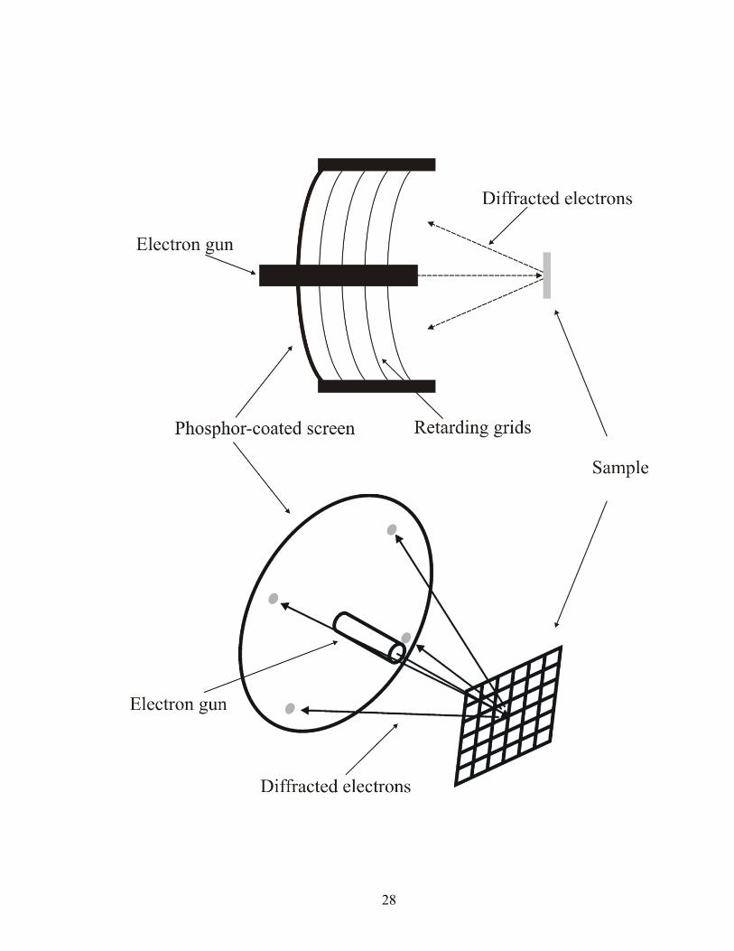
To ensure that the surface of interest is atomically ordered, low-energy electron
diffraction is employed. LEED utilizes a beam of low-energy electrons to probe the
periodicity of the surface of the electrode. This beam is emitted from an electron gun
housed in the center of the spherical LEED optics (Figure 1.10). Surrounding the
electron gun is a series of hemispherical, metal grids. As the electrons diffract off of the
surface, they are accelerated toward a phosphor-coated screen. Once the electrons strike
the screen, the phosphor-material begins to glow, creating the LEED pattern. The grids
in-between the phosphor screen and the crystal act as retarding filters, to only allow the
elastically scattered electrons to pass to the screen. This also allows a method to select,
by energy, which electrons reach the screen.
If the surface is well-ordered on the atomic level, the atoms act as a two-
dimensional diffraction grid. This produces a pattern of spots on the phosphor grid. This
pattern is indicative of the probed surface. For example, if a (100), or square lattice,
surface is analyzed with LEED, the pattern produced will be a square diffraction pattern
(Figure 1.11). Spots created by the underlying substrate are termed integral beams, while
spots resulting from the adlayer periodicity are called fractional-order beams. The
reflected beam from the electron in the center of the pattern is called the specular beam.
To analyze a LEED pattern, vectors are produced from the specular beam to both
the integral beams and the fractional-order beams. The proportion of the fractional-order
vector to the integral vector is inversely proportional to the distances on the surface of the
electrode. This means that smaller vectors in the LEED pattern are produced by larger
distances on the surface. The angle produced by the fractional-order vector and the
integral vector are the actual angle of the adlayer in relation to the substrate lattice. For

27
Figure 1.10 Low-energy electron diffraction.
28

29
Figure 1.11 Vector analysis using LEED patterns.

30

31
example, a (√2 x √2)R45° on a (100) substrate will produce a pattern with fractional-
order beams that are rotated 45° from the integral beams. The distance from the specular
beam to the fractional-order beams is √2/2 times the distance between the specular beam
and the integral beams, or the inverse of √2.
The analysis of LEED patterns can provide the periodicity, or the unit cell, of the
adlayer. It cannot supply the actual structure of the adsorbed layer. If all the adatoms do
not define the boundaries of the basic unit cell, they do not contribute to the LEED
pattern. A structure may have a higher actual coverage than the unit cell predicts. It is
imperative that LEED be performed in conjunction with a technique that can measure
either the basis of the adlayer, or the actual coverage of the layer with respect to the
underlying substrate. Auger electron spectroscopy can be performed analytically to give
an estimate of the coverage, which can be combined with the unit cell measured by
LEED to produce the actual basis of the adlayer. The coverage of the deposited layer can
also be calculated from coulometry measurements made during the electrodeposition.
Electrodeposition is performed in the antechamber of the UHV-EC instrument
(Figure 1.12). This stainless steel antechamber is connected to the main, surface-analysis
chamber by a gate valve. The crystal can be transferred to the antechamber by the means
of a manipulator arm. Once the crystal is inside the antechamber, the chamber can be
isolated from the vacuum and backfilled to atmospheric pressure with ultra-pure argon
(Figure 1.12a). Once at atmospheric pressure, the electrochemical cell is introduced to
the chamber through a transfer system located behind a gate valve on the underside of the
antechamber (Figure 1.12b).

32
Figure 1.12 The electrochemical experiment.

33
34
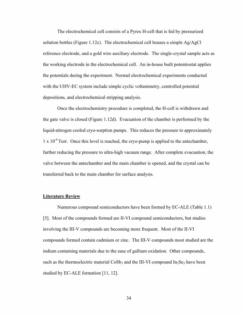
The electrochemical cell consists of a Pyrex H-cell that is fed by pressurized
solution bottles (Figure 1.12c). The electrochemical cell houses a simple Ag/AgCl
reference electrode, and a gold wire auxiliary electrode. The single-crystal sample acts as
the working electrode in the electrochemical cell. An in-house built potentiostat applies
the potentials during the experiment. Normal electrochemical experiments conducted
with the UHV-EC system include simple cyclic voltammetry, controlled potential
depositions, and electrochemical stripping analysis.
Once the electrochemistry procedure is completed, the H-cell is withdrawn and
the gate valve is closed (Figure 1.12d). Evacuation of the chamber is performed by the
liquid-nitrogen cooled cryo-sorption pumps. This reduces the pressure to approximately
1 x 10⁻⁴ Torr. Once this level is reached, the cryo-pump is applied to the antechamber,
further reducing the pressure to ultra-high vacuum range. After complete evacuation, the
valve between the antechamber and the main chamber is opened, and the crystal can be
transferred back to the main chamber for surface analysis.
Literature Review
Numerous compound semiconductors have been formed by EC-ALE (Table 1.1)
[5]. Most of the compounds formed are II-VI compound semiconductors, but studies
involving the III-V compounds are becoming more frequent. Most of the II-VI
compounds formed contain cadmium or zinc. The III-V compounds most studied are the
indium containing materials due to the ease of gallium oxidation. Other compounds,
such as the thermoelectric material CoSb3 and the III-VI compound In2Se3 have been
studied by EC-ALE formation [11, 12].

35
Table 1.1 Compound semiconductors formed by EC-ALE.

36
Compound Study Refs. ZnTe TLEC [13] ZnSe TLEC [13] ZnSe Flow cell deposition [14] ZnS Flow cell deposition [15] ZnS TLEC [13] ZnS STM studies of monolayers [11] ZnS Growth of superlattice [16] ZnS Size quantized film, photoelectrochemistry [17]
CdTe UHV-EC of first few monolayers [18] CdTe UHV-EC of first few monolayers [19] CdTe UHV-EC of first few monolayers [20] CdTe STM studies [21] CdTe STM and UHV-EC studies [22] CdTe Flow cell deposition [23] CdTe Review [24] CdTe Flow cell deposition, H-cell deposition [25] CdTe Flow cell deposition, H-cell deposition [26] CdTe UHV-EC and in-situ STM studies [27] CdTe Wall-jet flow cell growth [28] CdSe STM studies [29] CdSe STM and UHV-EC studies [30] CdSe Flow cell deposition, H-cell deposition [25] CdSe SERS [31] CdSe Flow cell deposition, large thin layer cell [32] CdS STM studies [33] CdS TLEC [34] CdS Voltammetry [35] CdS STM studies [36] CdS STM, RRDE studies [37] CdS STM, surface studies [38] CdS Flow cell deposition, H-cell deposition [25] CdS STM, voltammetry studies [39] CdS Raman spectroscopy studies [40] CdS Photoelectrochemical studies [41] CdS Resonance Raman studies [42] CdS Photoluminescence studies [43] CdS Growth of superlattice [16] HgS Photoluminescence study of a heterojunction [43]
GaAs UHV-EC studies [44] GaAs UHV-EC studies [45] InAs Thin films with TLEC flow system [46] InSb Thin films with TLEC flow system [47]
CuInSe2 TLEC [48] InSe Flow cell deposition [12]
CdS/HgS Photoluminescence study of a heterojunction [43] CdS/ZnS Growth of a superlattice [16]
CdS/CdSe Growth of a superlattice, SERS studies [31] InAs/InSb Growth of a superlattice [47]
37
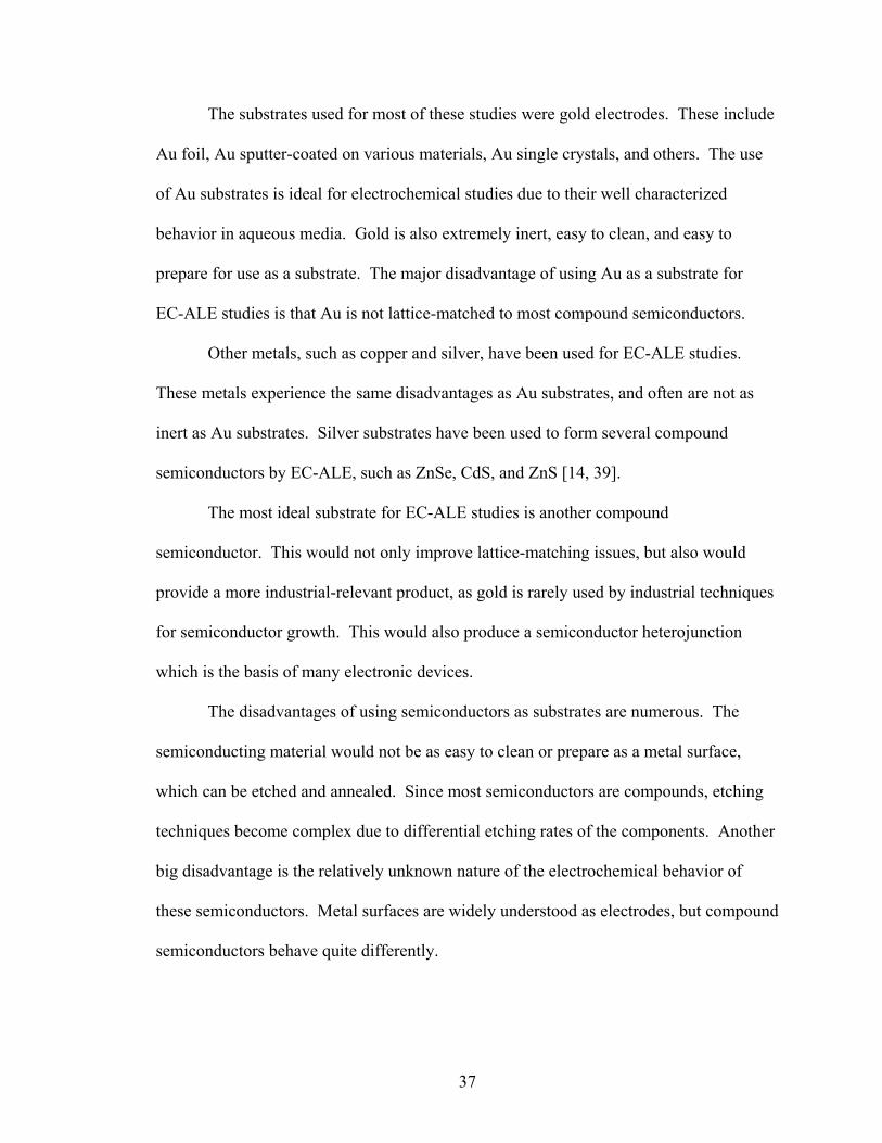
The substrates used for most of these studies were gold electrodes. These include
Au foil, Au sputter-coated on various materials, Au single crystals, and others. The use
of Au substrates is ideal for electrochemical studies due to their well characterized
behavior in aqueous media. Gold is also extremely inert, easy to clean, and easy to
prepare for use as a substrate. The major disadvantage of using Au as a substrate for
EC-ALE studies is that Au is not lattice-matched to most compound semiconductors.
Other metals, such as copper and silver, have been used for EC-ALE studies.
These metals experience the same disadvantages as Au substrates, and often are not as
inert as Au substrates. Silver substrates have been used to form several compound
semiconductors by EC-ALE, such as ZnSe, CdS, and ZnS [14, 39].
The most ideal substrate for EC-ALE studies is another compound
semiconductor. This would not only improve lattice-matching issues, but also would
provide a more industrial-relevant product, as gold is rarely used by industrial techniques
for semiconductor growth. This would also produce a semiconductor heterojunction
which is the basis of many electronic devices.
The disadvantages of using semiconductors as substrates are numerous. The
semiconducting material would not be as easy to clean or prepare as a metal surface,
which can be etched and annealed. Since most semiconductors are compounds, etching
techniques become complex due to differential etching rates of the components. Another
big disadvantage is the relatively unknown nature of the electrochemical behavior of
these semiconductors. Metal surfaces are widely understood as electrodes, but compound
semiconductors behave quite differently.
38
Progress has been made toward the use of compound semiconductors as
substrates for electrochemical deposition studies. Cadmium selenide has been deposited
on InP and GaAs substrates using codeposition methods [49, 50]. Indium tin oxide-
coated glass has been used as a substrate for the formation of ZnS and CdTe [15].
Cited References
1. A. Y. Cho, J. Vac. Sci. Tech., 1971, 8, p. s31. 2. A. Y. Cho and J. R. Arthur, Prog. Solid State Chem., 1975, (10), p. 157. 3. J. R. Arthur, J. Appl. Phys., 1968, 39, p. 4032. 4. M. B. Panish and H. Temkin, Ann. Rev. Matr. Sci., 1989, 19, p. 209. 5. J. L. Stickney, in Advances in Electrochemical Science and Engineering, ed. R. C. Alkire and D. M. Kolb, Wiley, New York, 2002. 6. J. L. Stickney, in Electroanalytical Chemistry, A. J. Bard and I. Rubenstein, Editors. 1999, Marcel Dekker: New York. 7. J. L. Stickney, B. W. Gregory, and I. Villegas, U. S. Patent, University of Georgia, 1994. 8. B. W. Gregory, D. W. Suggs, and J. L. Stickney, J. Electrochem. Soc., 1991, 138, p. 1279. 9. B. W. Gregory and J. L. Stickney, J. Electroanal. Chem., 1991, 300, p. 543. 10. M. P. Soriaga and J. L. Stickney, Vacuum Surface Techniques in Electroanalytical Chemistry, in Modern Techniques in Electroanalysis, ed.
P. Vanysek, Wiley, New York, 1996, p. 1-58. 11. A. Gichuhi, C. Shannon, and S. S. Perry, Langmuir, 1999, 15, p. 5654.

39
12. R. Vaidynathan, J. L. Stickney, and U. Happek, 2002, p. in prep. 13. L. P. Colletti, S. Thomas, E. M. Wilmer, and J. L. Stickney, MRS Symp. Boston, 1996, 451, p. 235. 14. G. Pezzatini, S. Caporali, M. Innocenti, and M. L. Foresti, J. Electrochem. Soc., 1999, 475, p. 164. 15. L. P. Colletti, R. Slaughter, and J. L. Stickney, J. Soc. Info. Display, 1997, 14, p. 87. 16. H. Yoneyama, A. Obayashi, S. Nagakubo, and T. Torimoto, Abstracts of the Electrochemical Society Meeting, 1999, 99-2, p. 2138. 17. T. Torimoto, A. Obayashi, S. Kuwabata, H. Yasuda, H. Mori, and H. Yoneyama, Langmuir, 2000, 16, p. 1513. 18. K. Varazo, M. Lay, T. A. Sorenson, and J. L. Stickney, J. Electroanal. Chem., 2002, 104, p. 11. 19. D. W. Suggs, I. Villegas, B. W. Gregory, and J. L. Stickney, J. Vac. Sci. Tech. A, 1992, 10, p. 886. 20. D. W. Suggs and J. L. Stickney, Surf. Sci., 1993, 290, p. 362. 21. D. W. Suggs and J. L. Stickney, Surf. Sci., 1993, 290, p. 375. 22. L. B. Goetting, B. M. Huang, T. E. Lister, and J. L. Stickney, Electrochim. Acta, 1995, 40, p. 143. 23. B. M. Huang, L. P. Colletti, B. W. Gregory, J. L. Anderson, and J. L. Stickney, J. Electrochem. Soc., 1995, 142, p. 3007. 24. C. K. Rhee, B. M. Huang, E. M. Wilmer, S. Thomas, and J. L. Stickney, Mater. and Manufact. Proc., 1995, 10, p. 283.

40
25. L. P. Colletti, B. H. Flowers, and J. L. Stickney, J. Electrochem. Soc., 1998, 145, p. 1442. 26. L. P. Colletti and J. L. Stickney, J. Electrochem. Soc., 1998, 145, p. 3594. 27. B. E. Hayden and I. S. Nandhakumar, J. Phys. Chem. B, 1998, 102, p. 4897. 28. I. Villegas and P. Napolitano, J. Electrochem. Soc., 1999, 146, p. 117. 29. T. E. Lister and J. L. Stickney, Appl. Surf. Sci., 1996, 107, p. 153. 30. T. E. Lister, L. P. Colletti, and J. L. Stickney, Isr. J. Chem., 1997, 37, p. 287. 31. S. Zou and M. J. Weaver, Chem. Phys. Lett., 1999, 312, p. 101. 32. B. H. Flowers, T. L. Wade, M. Lay, J. W. Garvey, U. Happek, and J. L. Stickney, J. Electroanal. Chem., 2001, 273, p. 13. 33. U. Demir and C. Shannon, Langmuir, 1996, 10, p. 2794. 34. L. P. Colletti, D. Teklay, and J. L. Stickney, J. Electroanal. Chem., 1994, 369, p. 145. 35. E. S. Streltsov, Dokl. Akad. Nauk. Bel., 1994, 38, p. 64. 36. U. Demir and C. Shannon, Langmuir, 1996, 12, p. 594. 37. U. Demir and C. Shannon, Langmuir, 1996, 12, p. 6091. 38. G. Aloisi, J. Phys. Chem. B, 1997, 101, p. 4774. 39. M. L. Foresti, G. Pezzatini, M. Cavallini, G. Aloisi, M. Innocenti, and R. Guidelli, J. Phys. Chem. B, 1998, 102, p. 7413. 40. A. Gichuhi, B. E. Boone, U. Demir, and C. Shannon, J. Phys. Chem. B, 1998, 102, p. 6499. 41. T. Torimoto, Langmuir, 1998, 14, p. 7077. 42. B. E. Boone, A. Gichuhi, and C. Shannon, Anal. Chim. Acta., 1999, 397, p. 43.

41
43. A. Gichuhi, B. E. Boone, and C. Shannon, Langmuir, 1999, 15, p. 763. 44. I. Villegas and J. L. Stickney, J. Vac. Sci. Tech. A, 1992, 10, p. 3032. 45. I. Villegas and J. L. Stickney, J. Electrochem. Soc., 1992, 139, p. 686. 46. T. L. Wade, L. C. Ward, C. B. Maddox, U. Happek, and J. L. Stickney, Electrochem. Sol. State Lett., 1999, 2, p. 616. 47. T. L. Wade, R. Vaidynathan, U. Happek, and J. L. Stickney, J. Electroanal. Chem., 2001, 322, p. 11. 48. R. D. Herrick and J. L. Stickney, 173, in New Directions in Electroanalytical Chemistry, ed. J. Leddy and M. Wightman, The Electrochemical Society: Pennington, New Jersey, 1996. 49. H. Cachet, R. Cortes, M. Froment, and G. Marurin, Philos. Mag. Lett., 1999, 79, p. 837. 50. L. Beaunier, H. Cachet, M. Froment, and G. Marurin, J. Electrochem. Soc., 2000, 147, p. 1835.

42
Chapter 2
ELECTRODEPOSITION OF SB ONTO THE LOW-INDEX PLANES OF CU IN AQUEOUS CHLORIDE SOLUTIONS: STUDIES BY LEED, AES, AND
ELECTROCHEMISTRY1
__________________ 1Ward, L. C. and J. L. Stickney, Phys. Chem. Chem. Phys., 2001, 3, 3364. Reproduced by permission of The Royal Society of Chemistry on behalf of the PCCP Owner Societies.

43
Abstract
The underpotential deposition (UPD) of Sb on Cu(111), Cu(100), and Cu(110)
has been studied using ultra-high vacuum electrochemistry (UHV-EC) techniques. Sb
was deposited from acidic chloride solutions and analyzed with Auger electron
spectroscopy (AES), low-energy electron diffraction (LEED), and cyclic voltammetry. A
feature observed only in the first voltammetric cycle, starting from the rest potential,
appears to be Sb UPD on the copper surfaces. Prior to Sb UPD, Cl structures were
observed on each of the three Cu planes. When the potential was scanned into the
transient reductive feature, antimony began to deposit, displacing the chlorine. Initially,
structures containing both Cl and Sb were formed on the Cu surfaces, including a
(√3x√3)R30° on the Cu(111), a (2√2x√2)R45° on the Cu(100), and a structure denoted in
matrix notation as
− 11
31 formed on Cu(110). Further Sb deposition results in
displacement of the chloride and new structures on each face: Cu(111)(3x√21),
Cu(110)(3x2), and Cu(100)(3x2). Scanning the deposition potential further negative, into
bulk Sb deposition, yielded no well-ordered structures.

44
Introduction
Antimony is an increasingly important element in the fields of electronics and
optoelectronics. Compound semiconductors containing Sb are used in the formation of
infrared (IR) photodetectors, lasers, thermophotovoltaic devices, and high-speed
electronic devices. Its use as a surfactant and dopant is increasingly important as well.
The III-V compound semiconductors GaSb and InSb are finding an increasing
number of applications in the manufacturing of long wavelength (> 1.5 mm) detectors, IR
detectors, and high-speed electronics [1, 2]. Other compound semiconductors containing
more than two elements, such as GaxIn1-xAsySb1-y, and InAsxSb1-x, can be used for
optoelectronic and transport devices [3-5].
The second area of semiconductor technology that antimony has shown
significance is in alloyed semiconductors. This field involves the formation of alloys of
group V and other elements to form semiconducting compounds. Examples of these
compounds include Sb2Te3, Sb2Se3, As-Sb alloys, and CsxSb [6-10]. Uses for compounds
in this area include photocathodes, photodectors, and thermoelectric devices.
An area of high interest for many years has been the use of antimony as a capping
layer on III-V compound semiconductors. This capping layer can act as a passivating
layer to prevent oxidation or other processes from occurring, or an intermediate layer for
the growth of a new compound. These capping layers can also provide information on
the growth mechanisms of compound semiconductors. Extensive research has been
performed depositing antimony on GaAs [11-18]. Antimony forms chain-like dimers
along the GaAs(110) surface [17]. This is similar to the effect of Bi on GaAs(110)
substrates [11]. These structures are referred to as epitaxial continued layer structures

45
(ECLS). The chains of the ECLS follow the substrate structure, consisting of antimony
atoms lying in troughs of the (110) surface [11]. Dimer formation is also evident for the
deposition of antimony on GaAs(100), but is less prominent than on the (110) surface
[14]. For the GaAs(111) surface, antimony deposition creates a surface reconstruction on
the substrate. Various reconstructions, such as (1 x 3) and (3 x 8), can occur depending
upon the amount of antimony deposited [13, 15]. Other semiconductor/antimony
interfaces that have been studied include InAs, ZnSe, GaP, InP, and InAlSb [19-24].
Antimony deposition on intrinsic semiconductors, like germanium and silicon,
has been studied for analogous reasons to those for its growth on compound
semiconductors [25-29]. The majority of the research in this area has been centered
around antimony deposition on silicon. These experiments are designed to probe the
surfactant effect of antimony on the growth of metals, given the quasi-metallic nature of
Sb. The desire is to form metallic films of metals such as Ag on Si, for example.
Doping of II-VI compound semiconductors can be accomplished by the
incorporation of antimony into the bulk lattice. Cadmium telluride electrodeposited from
non-aqueous solutions can be doped with antimony [30]. This creates p-type CdTe with
few oxygen impurities, due to the oxygen arresting characteristic of antimony. Other
semiconductor materials, like SnO2, can be doped by antimony incorporation as well
[31].
An interesting area of research concerning antimony deposition is in the
surfactant field. Antimony has shown a surfactant effect for the deposition of various
metals on a number of substrates [26, 32-36]. The majority of the literature work
involves silver deposition, usually on a silver substrate. It is thought that the antimony

46
poisons the silver surface, causing the mobility of the silver adatoms to decrease. This
forces the silver atoms to forms islands on the substrate, that then coalesce into an
epitaxial film [33].
The study presented here involves the deposition of antimony on the low-index
planes of copper. While this system has not been studied electrochemically, many
surface segregation experiments have been reported [37-44]. An antimony doped copper
single crystal has been used to study the surface structure of this sub-monolayer coverage
of antimony. Scanning tunneling microscopy (STM) and UHV surface analysis have
shown that a (√3x√3)R30° antimony/copper surface alloy forms on the Cu(111) surface
[37, 39, 40]. This alloy consists of antimony atoms sitting in a copper lattice at nominal
√3 positions. This alloy has been confirmed by medium energy ion scattering (MEIS)
techniques [44]. Several structures arise from the antimony/copper (100) system,
depending upon the temperature at which the antimony alloyed copper single crystal is
annealed. These structures include (7√2x√2)R45°, (2x2), and (√5x√5)R26° unit cells. It
appears that the structures are actually alloys, as opposed to adsorbed adlayers [41].
The underpotential deposition (UPD) of antimony could provide a viable
technique for the electrochemical deposition of antimony containing compound
semiconductors. The underpotential deposition phenomenon involves the
electrochemical deposition of a surface limited layer of an element onto a substrate. With
certain systems, this first atomic layer is energetically more stable than multiple layers of
the element. This UPD layer deposits at a potential prior to that needed to deposit the
bulk element. If the potential is held at the UPD value, an atomic layer can deposit at
equilibrium, without the formation of bulk, as the reaction is self-terminating. If two

47
elements can be deposited by separate UPD processes, an epitaxial compound can be
formed using a cycle. This process is the electrochemical analog of atomic layer epitaxy
(ALE), referred to here as electrochemical atomic layer epitaxy (EC-ALE) [45, 46]. EC-
ALE has been used to form a variety of compound semiconductors [47-49]. Progress in
the formation of compounds and materials using EC-ALE is directly dependent on
understanding the atomic layer formation steps needed to form the deposition cycle.
Recently, deposits of InSb have been formed using EC-ALE, and the cycle has been
incorporated into the formation of InAs/InSb superlattices [50]. Other compound
semiconductors that have been formed by EC-ALE include: CdTe, CdS, and CdSe [51-
57].
Experimental
Studies were conducted with a Cu single crystal that has been cut and polished,
forming facets of the three low index planes, (111), (100), and (110), present on one
single crystal (Figure 2.1)[58]. The three faces are oriented along the vertical axis of the
crystal, allowing all three planes to be analyzed in sequence by simply rotating the
crystal. The major benefit is that it provides a direct comparison of the structures formed
on the Cu low-index planes, formed under a given potential program.
The studies presented here were performed using ultra-high vacuum
electrochemical methodologies (UHV-EC)[59], where the principle is to use a UHV
surface analysis instrument, directly coupled to a stainless steel antechamber that houses
an electrochemical cell apparatus. This antechamber can be isolated from the main
surface analysis chamber and backfilled with ultra-high purity argon before each

48
Figure 2.1 Cartoon of the copper tri-crystal.

49

50
electrochemical experiment. This allows the direct transfer of the electrodeposited
material to the UHV surface analysis chamber, avoiding contamination from air.
This UHV instrument was equipped with a cylindrical mirror analyzer (CMA) for
Auger electron spectroscopy (Physical Electronics), optics for low energy electron
diffraction (Princeton Electronics), a quadrupole mass analyzer for residual gas analysis
(UTI), and an ion gun for cleaning the crystal by ion bombardment (Physical
Electronics). The chamber was ion pumped, and a cryo-pump was used to evacuate the
antechamber. This cryo-pump was selected due to its high pumping speed of water
vapor. The base pressure of the system was usually in the 10-9 Torr range, but consisted
mostly of Ar and water vapor, which did not interfere with our studies.
Before each electrochemical experiment, the Cu single crystal was cleaned by Ar
ion bombardment, followed by annealing to repair damage to the crystal surface. The
cleanliness was confirmed by AES and observation of clean surface LEED patterns.
Potentials were measured versus a Ag/AgCl (3M NaCl) reference electrode
(BAS), and the auxiliary electrode was a gold wire (Wilkinson Company). The
potentiostat, based on simple op-amp circuitry, was constructed in-house, and was used
for voltammetry and the control of electrode potentials. The Sb solution consisted of
0.1 mM Sb (Sb2O3, 99.999% Aldrich), and 1 mM HCl (reagent grade, J. T. Baker). An
acidic solution was used not only to facilitate the dissolution of the Sb2O3, but also to
prevent the formation of CuOx species during experiments. Ultra-pure (18 MΩ) water
from a nanopure filtration system (Barnstead), fed from the house-deionized water
supply, was used to prepare the antimony solution.

51
The electrochemical hardware consisted of a Pyrex H-cell housed in a stainless
steel cylinder. This allowed the cell to be purged with ultra-pure Ar prior to each
electrochemical experiment. The cell was introduced into the EC-antechamber, which
was backfilled to atmospheric pressure with ultra-pure Ar, through a gate valve at the
bottom. Solutions were pumped into the H-cell by pressurizing the Pyrex solution
reservoirs. Each bottle was equipped with a glass-tee with a three-way stopcock, allowing
solution delivery and its subsequent draining.
After Sb deposition, the solutions were drained, the electrochemical cell was
withdrawn, the gate valve closed, and the EC-antechamber was evacuated using
cryosorption pumps and the cryo-pump. Upon reaching ultra-high vacuum, the crystal
was transferred back into the main chamber for surface analysis. AES spectra, with
3000 eV ionizing electrons, were collected for each face of the crystal, for kinetic
energies between 100–1100 eV. LEED patterns were recorded for each plane using a
Kodak digital camera (Model DC290).
Results and Discussion
Cyclic voltammetry for the clean, annealed copper tri-crystal in the Sb solution is
shown in Figure 2.2. The scans were started at the rest potential, -0.057 V, and then
scanned between -0.7 V and +0.1 V for two cycles. A scan rate of 5 mV/sec was used.
The first reduction feature, at -0.1 V, is due to a small amount of dissolved copper
re-depositing onto the electrode surface. The broad reduction shoulder at -0.4 V appears
only in the first scan. This feature was never observed in subsequent scans, regardless of

52
Figure 2.2 Cyclic voltammogram of the Cu electrode in 0.1 mM Sb in 1 mM HCl
(pH = 3) supporting electrolyte: scan rate = 5 mV s-1.

53
54
how far positive the oxidation potential was scanned. This reduction is believed to be the
underpotential deposition of antimony onto the copper electrode. Oxidation of the UPD
antimony does not occur with these conditions, as copper dissolution takes place first,
depolarizing the electrode, and preventing the dissolution of the last atomic layer of Sb.
The reduction feature at -0.600 V and the oxidation feature at 0.000 V are the deposition
and stripping of bulk Sb, respectively.
In the studies presented here, antimony was deposited on the clean copper crystal
by immersion in the solution at a series of controlled potentials. Each deposition was
performed for two minutes. The resulting coulometric data is shown in Figure 2.3, where
a short plateau is evident between –0.200 V to –0.300 V, suggesting surface limited
deposition, consistent with UPD. After this plateau, the coverage increases to near 1.0
and continues to rise, at potentials below –0.400 V. The currents measured in each
experiment are the result of not only the deposition of antimony on each low index plane,
but also of the reductive dissolution of an adsorbed monolayer of chlorine. This masks
the Sb coverage based coulometry, although the charges provide an estimation of
expected coverages.
Auger spectra for each of the three low index planes were collected after each
emersion experiment. At potentials positive of -0.2 V, only chlorine and copper were
evident, with very little antimony present (coverages less than 0.15 ML). The small
amount that was present appears to have been antimony oxide adsorbed to the surface.
This is evident due to the oxygen signal present in the Auger spectra. At potentials more
negative than -0.200 V, reduced antimony began to deposit on the electrode, with a

55
Figure 2.3 Coverage calculated by coulometric data vs. deposition potential.

56

57
corresponding decrease in the chlorine coverage. This decrease in the Cl signal varies
between the three faces. On the Cu(111), the chlorine intensity dropped to near zero, but
significant signal was still present for the Cu(100) and Cu(110) throughout the potential
range used in these studies.
Figure 2.4 shows four typical Auger spectra at various emersion potentials for the
Cu(111) surface. Auger peak heights for antimony, chlorine, and copper were measured
for each spectrum and used to calculate Auger peak ratios for antimony/copper and
chlorine/copper. These ratios were then plotted versus the corresponding deposition
potential. The copper peak at 920 eV, the chlorine peak at 181 eV, and the antimony
peak at 454 eV were chosen for the Auger peak measurements. Since coulometric data
could not be used to accurately predict coverages in these experiments, the Auger peak
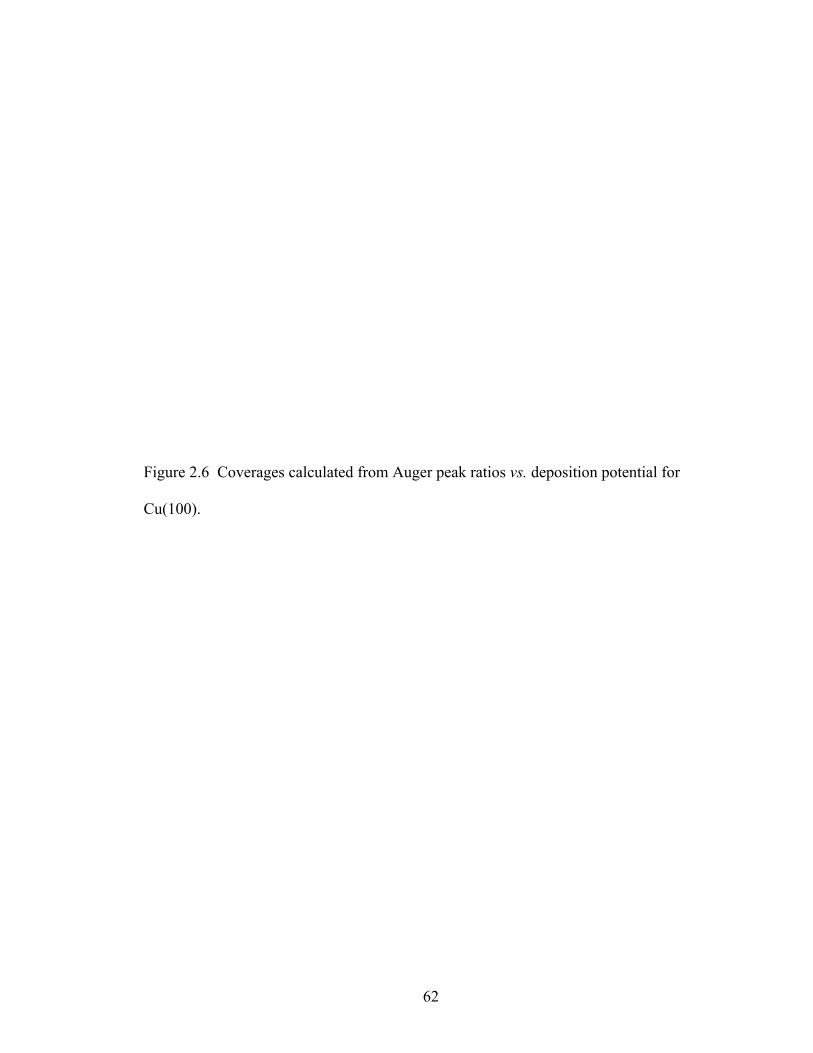
ratios were converted into coverages. This was accomplished by assuming that at -0.057
V the Cl coverage for the Cu(111) surface is 0.33. This was confirmed by LEED and by
the literature [60-62]. Using this coverage and the corresponding Auger peak ratio, the
remaining Auger peak ratios were converted into coverages for each low-index plane.
Similarly, the Sb coverage at -0.300 V, from LEED and literature values, was assumed
to be 0.33 [37]. The Sb/Cu Auger peak ratios were then converted to coverages in the
same manner as the Cl/Cu ratios. These coverages were plotted versus the deposition
potential for all three low index planes (Figures 2.5-2.7). These coverages, combined
with the LEED data (Figures 2.8-2.10), were used to construct the proposed structures for
each face (Figures 2.11-2.13).
Chlorine has been shown to deposit spontaneously on Cu surfaces over a wide
range of potentials [60-65]. At potentials positive of -0.200 V, Cl is present on all three

58
Figure 2.4 AES spectra for Sb/Cl deposition on the Cu(111) surface of the copper
electrode at various deposition potentials.

59

60
Figure 2.5 Coverages calculated from Auger peak ratios vs. deposition potential for
Cu(111).

61
62
Figure 2.6 Coverages calculated from Auger peak ratios vs. deposition potential for
Cu(100).

63

64
Figure 2.7 Coverages calculated from Auger peak ratios vs. deposition potential for
Cu(110).

65

66
Figure 2.8 LEED patterns for the Cu(111) surface. Deposition potential: (a) -0.057,
(b) -0.200, (c) -0.300, (d) -0.350 V.

67
68
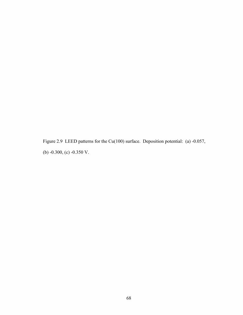
Figure 2.9 LEED patterns for the Cu(100) surface. Deposition potential: (a) -0.057,
(b) -0.300, (c) -0.350 V.

69

70
Figure 2.10 LEED patterns for the Cu(110) surface. Deposition potential: (a) -0.057,
(b) -0.300, (c) -0.350 V.
71

72
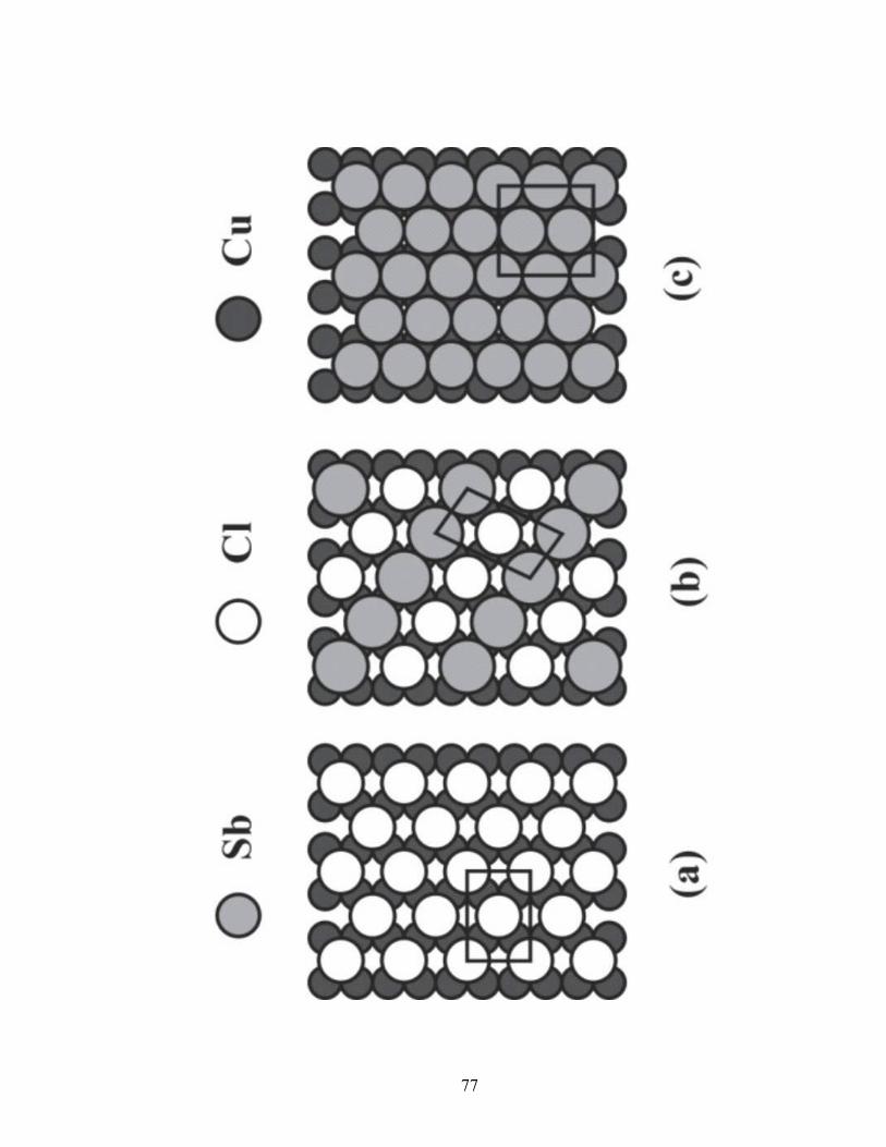
Figure 2.11 Proposed structures for the Cu(111) surface adlayers. (a) Cl “split-spot”
(√3x√3)R30°, (b) Sb/Cl transition (√7x√7)R19.1°, (c) Sb (√3x√3)R30°.
73

74
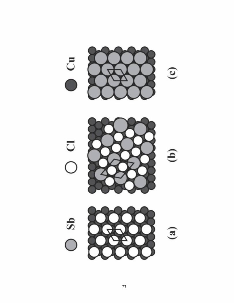
Figure 2.12 Proposed structures for the Cu(100) surface adlayers. (a) Cl (√2x√2)R45°,
(b) Sb/Cl (2√2x√2)R45°, (c) Sb (3x2).

75

76
Figure 2.13 Proposed structures for the Cu(110) surface adlayers. (a) Cl c(2x2),
(b) Sb/Cl matrix denoted, (c) Sb (3x2).
77

78
Cu planes. A “split-spot” (√3x√3)R30° LEED pattern was observed for the Cu(111)
surface (Figure 2.8a). This “split-spot” pattern has a group of spots, three to six, near the
LEED pattern’s √3 positions. The splitting of the spots has been explained elsewhere by
√3 local symmetry inside a larger unit cell with phase boundaries [60, 66]. This has been
observed for other systems, such as iodine adsorption on Cu and silver, and tellurium
adsorption on gold [48, 67-69]. It is also observed that the “split-spot” pattern is only
observed ex-situ and not while imaged in solution with a scanning tunneling microscope
[70]. Since the LEED experiments were conducted ex-situ, the proposed structure
derived is the split-spot (√3x√3)R30° (Figure 2.11a).
On the Cu(100) surface, a (√2x√2)R45° structure is formed by the Cl adlayer
(Figure 2.9a). This structure is equivalent to the c(2x2) structure seen in gas-phase Cl
dosing studies of Cu(100) [60]. The coverage versus deposition potential plot indicates a
coverage of 0.5, which agrees well with previous work, and the symmetry of the LEED
pattern. The proposed structure for this Cl adlayer is shown in Figure 2.12a.
The LEED pattern for the Cu(110) surface coated with Cl is streaky, consisting of
a series of broad lines (Figure 2.10a). This pattern is representative of a c(2x2) structure.
The explanation for this diffuse pattern is that there are multiple, unit cells
simultaneously distributed across the (110) surface [60]. This structure is probably due to
chains of Cl atoms in the troughs of the corrugated Cu surface. These atoms are free to
move along the troughs, producing a variety of unit cells and thus the streaks in the
LEED pattern. A simple c(2x2) structure yields a coverage value equal to 0.5 (Figure
2.13a). The coverage for this proposed structure is consistent with the Auger data (Figure
2.7).
79
At approximately -0.200 V, a (√7x√7)R19.1° pattern begins to mix into the “split-
spot” Cl pattern for the Cu(111) (Figure 2.8b). Auger shows an increased Sb signal for
this deposition potential, and the intensity of the Cl peaks begins to decrease. The √7
spots that appear in the LEED pattern are believed to be due to the incorporation of Sb
into the adlayer of Cl. The proposed structure at this potential has Cl maintaining its
(√3x√3)R30° lattice, while the Sb is beginning to form structural domains with
(√7x√7)R19.1° symmetry, displacing some of the Cl (Figure 2.11b). Coverages for both
the Sb and the Cl agree between the proposed structure and the Auger peak ratios.
Alternatively, the Sb may just insert into the (√3x√3)R30° lattice, creating a larger unit
cell that contains both Sb and Cl atoms. This would be a good system for study using
scanning tunneling microscopy.
The Cu(100) surface shows no change at -0.200 V from its original (√2x√2)R45°
coverage. Auger spectroscopy does show a small Sb signal at this potential, but the
LEED pattern is unchanged. LEED patterns for the Cu(110) face at -0.200 V show no
discernible pattern. Many highly diffuse spots are present in these patterns, but no clear
structure is visible. This pattern is thought to be a transition from the c(2x2) to a different
pattern containing both Cl and Sb, due to the increase in the Sb Auger signal.
At an emersion potential of -0.300 V, a sharp (√3x√3)R30° LEED pattern is
present for the Cu(111) surface (Figure 2.8c). No splitting of the LEED spots is
observed. This pattern is consistent with scanning tunneling microscopy data for the
surface segregation of Sb on Cu(111)[37, 39]. Aufray and co-workers discovered
evidence of an Sb/Cu alloy phase in their STM studies. The Sb occupied positions
equivalent to a (√3x√3)R30° adlayer, but the atoms were actually bound into the first

80
layer of the Cu substrate. This phenomenon can neither be proved nor disproved by the
data presented here. While the Cl Auger signal has diminished substantially, a significant
amount of Cl is still present upon the surface. It is not known if this Cl is incorporated
into the proposed (√3x√3)R30° structure (Figure 2.11c).
The Cl/Cu and Sb/Cu Auger peak ratios are nearly equal for the Cu(110) face at
-0.300 V. LEED displays a well-defined pattern (Figure 2.10b) at this potential,
apparently related to the (2√2x√2)R45° structure formed on Cu(100). This pattern is
described using matrix notation as:
− 11
31. From the coverage versus potential graphs,
the structure should be composed of 0.25 coverages for both Sb and Cl. The unit cell,
derived from the LEED, is consistent with these coverages as well, implying the Cl and
the Sb may form overlapping structures with the same unit cell (Figure 2.13b).
For the Cu(100), a new structure is also observed at -0.300 V. The LEED pattern
is a (2√2x√2)R45° for the Sb/Cl layer (Figure 2.9b). The Cl signal in the Auger spectrum
is decreased, but is still prominent. Coverages for both the Sb and Cl are both
approximately 0.4 (Figure 2.6), slightly higher than the 0.25 coverages in the proposed
structure for this potential (Figure 2.12b).
At a deposition potential of -0.350 V, a (3x2) LEED pattern is observed for the
deposited Sb on Cu(100) (Figure 2.9c). The Sb coverage calculated from the Auger peak
ratios is approximately 0.5, while the Cl is 0.25 (Figure 2.6). The proposed structure is a
simple (3x2) unit cell with an extra Sb atom centered in the cell (Figure 2.12c). This
gives a coverage of only 0.33 for the Sb. While this is slightly lower than the Auger
coverage, it was the only logical structure devised that was consistent with the unit cell.

81
The explanation for the discrepancy between the LEED and Auger peak ratios is not
known.
At -0.350V, the Cu(111)(√3x√3)R30°-Sb structure changes to a (3x√21) unit cell
(Figure 2.8d). According to Auger, the Sb coverage is approximately 0.75. No logical
structure has been devised as yet to account for this coverage and the (3x√21) unit cell.
One possibility for this unusual coverage is alloy formation. It has been reported through
segregation experiments that Sb will alloy into the first layer of the Cu single crystal [37,
39, 40]. This forms an SbCu2 alloy layer, with the Sb atoms sitting within √3 sites in the
lattice as discussed above. If a second layer of pure antimony deposits upon this alloy,
the (3x√21) unit cell may be formed giving a total Sb coverage of near 0.75. It is
assumed that the Sb arranges in a hexagonal overlayer, but the exact structure cannot be
determined from LEED and AES alone. Further STM studies are needed to fully
understand this coverage.
The 0.25 coverage
− 11
31 unit cell for the Cu(110) changes to a more densely
packed adlayer at -0.400 V. This new structure gives a (3x2) LEED pattern (Figure
2.10c). The Auger plots suggest an Sb coverage of approximately 0.66 at this potential.
This yields a proposed structure that is identical to the high-density coverage for Cl
adsorbed on Cu(110) (Figure 2.13c) [60]. The Cl coverage is diminished, but still
present. Again, it is not known where this Cl resides in this structure.
Beyond -0.450 V, no discernible LEED patterns are visible for the three low-
index planes. It is assumed that beyond this potential the Sb deposition is mass transfer
82
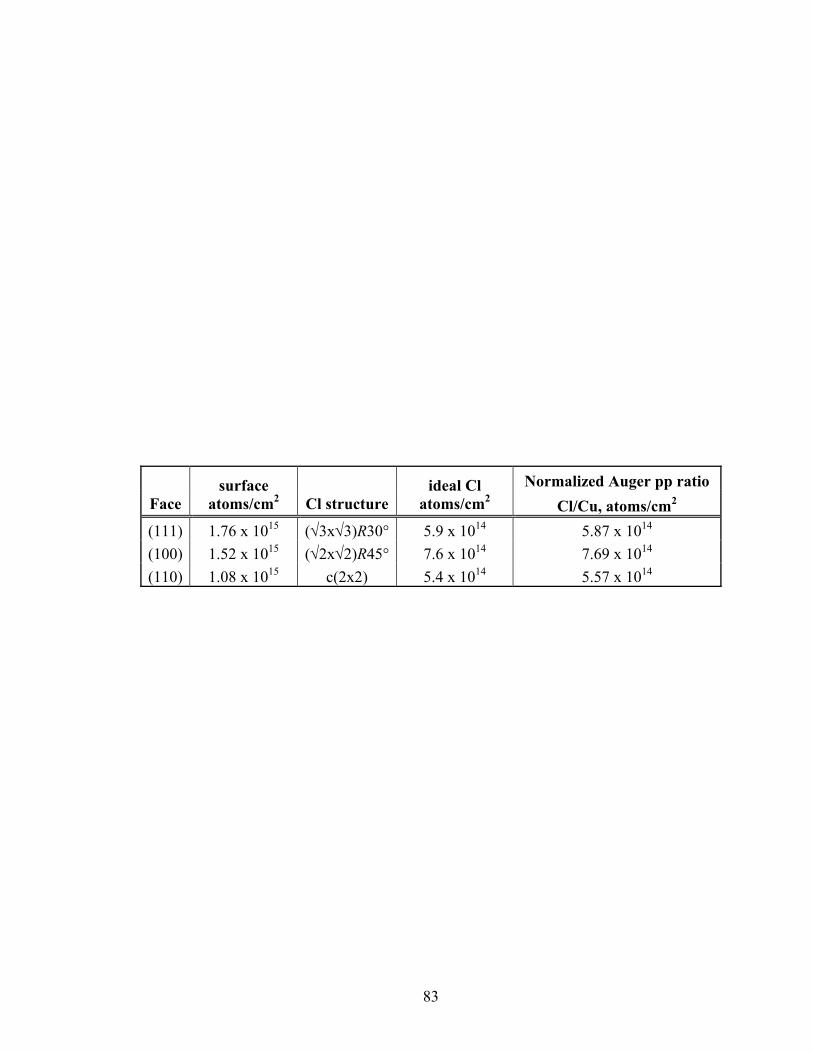
Table 2.1 Chlorine structures and coverages: ideal and experimental.
83
Normalized Auger pp ratio Face
surface atoms/cm2 Cl structure
ideal Cl atoms/cm2 Cl/Cu, atoms/cm2
(111) 1.76 x 10¹⁵ (√3x√3)R30° 5.9 x 10¹⁴ 5.87 x 10¹⁴ (100) 1.52 x 10¹⁵ (√2x√2)R45° 7.6 x 10¹⁴ 7.69 x 10¹⁴ (110) 1.08 x 10¹⁵ c(2x2) 5.4 x 10¹⁴ 5.57 x 10¹⁴

84
controlled, not UPD. Coverages for the Sb in this range exceed 1.0 and the Cl coverages
are reduced to nearly zero.
Table 2.1 shows the ideal and experimental coverages for the Cl structures. Good
correlation exists between the theoretical and measured values. These results also agree
closely with previous work on the exposure of Cu single crystals to gaseous Cl2 and
aqueous Cl- solutions [60, 64].
Ideal and experimental coverages for the Sb structures are tabulated in Table 2.2.
Correlations between the ideal and experimental values vary for each surface. For
Cu(111), the 0.33 coverage (√3x√3)R30° structure, experimental and ideal values have to
match due to the assumption made in calculating the theoretical coverages. The (3x√21)
structure gives a coverage that is nearly twice the ideal 0.33 coverage, clearly
illuminating the fact that the unit cell basis is not well understood.
Both the (2√2x√2)R45° on Cu(100) and the matrix denoted structure on Cu(110)
show lower experimental coverages when compared to the ideal structures. This is
probably related to the finite amount of Cl adsorbed on the surface. The presence of Cl
on the surface may in some way limit the Sb coverage, relative to the ideal value. This
also appears to happen in the (3x2) structures on both Cu(100) and Cu(110). It is
proposed that the Cl has the same unit cell as the Sb for the (2√2x√2)R45° and matrix
denoted structures. The actual placement of the Cl on the two (3x2) structures is not
known and is clearly an area where STM studies are needed.

85
Table 2.2 Antimony structures and coverages: ideal and experimental.

86
Normalized Auger pp ratioFace
surface atoms/cm2 Sb structure
ideal Sb atoms/cm2 Sb/Cu, atoms/cm2
(111) 1.76 x 10¹⁵ (√3x√3)R30° 5.9 x 10¹⁴ 5.87 x 10¹⁴ (100) 1.52 x 10¹⁵ (2√2x√2)R45° 7.6 x 10¹⁴ 3.90 x 10¹⁴ (110) 1.08 x 10¹⁵ matrix denoted 5.4 x 10¹⁴ 3.91 x 10¹⁴ (111) 1.76 x 10¹⁵ (3x√21) 5.9 x 10¹⁴ 1.36 x 10¹⁵ (100) 1.52 x 10¹⁵ (3x2) 7.6 x 10¹⁴ 5.33 x 10¹⁴ (110) 1.08 x 10¹⁵ (3x2) 7.2 x 10¹⁴ 6.48 x 10¹⁴

87
Conclusions
Antimony atomic layers have been electrodeposited from acidic chloride solutions
onto the low-index planes of Cu by UPD. Cl initially deposits as well-ordered structures
on the Cu single crystal forming a (√3x√3)R30° on Cu(111), a (√2x√2)R45° on Cu(100),
and a c(2x2) on Cu(110). Those structures are present until the onset of Sb deposition.
Each plane of the Cu single crystal forms a transition structure composed of both Sb and
Cl, beginning at about –0.200 V.
As the potential is scanned to more negative values, the Sb coverage increases and
the Cl coverage decreases. On the Cu(111) surface, the Sb adlayer forms a (√3x√3)R30°
structure with a small amount of Cl still present. This structure is present until the onset
of a (3x√21) unit cell at –0.350 V. At this point, the Cl coverage is nearly zero and the
Sb coverage is approximately 0.75. The basis for this unit cell is not known, and STM
data is needed.
The Cu(100) (2√2x√2)R45° transition structure changes into a (3x2) unit cell at
-0.350 V. This structure gives an Sb coverage of 0.5, while the Cl is at 0.25. The ideal
coverage for this unit cell is 0.33. The reason for the discrepancy between these values is
unknown.
The matrix denoted structure for the Sb adlayer on Cu(110) transforms into a
(3x2) structure upon further Sb deposition at –0.400 V. The calculated coverage and
experimental coverage values are approximately equal at 0.67. A small amount of Cl,
about 0.2 ML, is still present on the surface, but it is not known how this Cl affects the
structure. Beyond –0.450 V, no well-ordered structures were observed, and the Sb
coverages increase above 1 ML.

88
These results demonstrate that a surface-limited reaction does occur in the
electrodeposition of Sb onto the low-index planes of Cu. A sequence of ordered
structures was observed on each of the low index planes. It is clear that the structures are
very dependent on the electrolyte, in this case Cl-. A well-defined UPD process does
take place, even though it is not present in the voltammetry.
Cited References
1. N. Jones, C. Norris, C. L. Nicklin, P. Steadman, S. H. Baker, A. D. Johnson, and
S. L. Bennett, Surf. Sci., 1998, 409, 27. 2. I. Nicoara, D. Nicoara, A. G. Ostrogorsky, C. Marin, and T. Peignier, J. Cryst.
Growth, 2000, 220, 1. 3. H. Baaziz, Z. Charifi, and N. Bouarissa, Matr. Chem. Phys., 2001, 68, 197. 4. S. Cattarin, M. M. Musiani, U. Casellato, P. Guerriero, and R. Bertoncello, J.
Electroanal. Chem., 1995, 380, 209. 5. J. J. Lee, and M. Razeghi, J. Cryst. Growth, 2000, 221, 444. 6. B. Erjavec, Thin Solid Films, 1997, 303, 4. 7. A. M. Fernandez, and M. G. Merino, Thin Solid Films, 2000, 366, 202. 8. M. M. Musiani, F. Paolucci, and P. Guerriero, J. Electroanal. Chem., 1992, 332,
113. 9. M. Monev, I. Krastev, and A. Zielonka, J. Phys.-Condens. Mat., 1999, 11, 10033. 10. R. Venkatasubramanian, T. Colpitts, E. Watko, M. Lamvik, and N. El-Masry, J.
Cryst. Growth, 1997, 170, 817. 11. P. Haier, P. V. Santos, N. Esser, and W. Richter, Surf. Sci., 1998, 399, 264.

89
12. P. V. Santos, N. Esser, J. Groenen, M. Cardona, W. G. Schmidt, and F. Bechstedt,
Phys. Rev. B, 1995, 52, 17379. 13. P. Moriarty, P. H. Beton, M. Henini, and D. A. Woolf, Surf. Sci., 1996, 365,
L663. 14. F. Maeda, Y. Watanabe, and M. Oshima, Surf. Sci., 1996, 357-358, 540. 15. A. A. Cafolla, C. McGinley, E. McLoughlin, G. Hughes, P. Moriarty, A. W.
Dunn, Y. R. Ma, D. Teehan, B. Murphy, S. Downes, and D. A. Woolf, Surf. Sci., 1997, 377-379, 130.
16. W. G. Schmidt, and F. Bechstedt, Surf. Sci., 1997, 377-379, 11. 17. C. Nowak, A. Hempelmann, A. Markl, A. Chasse, E. Dudzik, C. Muller, I. T.
McGovern, W. Braun, W. Richter, and D. R. T. Zahn, Surf. Sci., 1995, 331-333, 564.
18. L. J. Whitman, B. R. Bennett, E. M. Kneedler, B. T. Jonker, and B. V.
Shanabrook, Surf. Sci., 1999, 436, L707. 19. V. Y. Aristov, M. Grehk, V. M. Zhilin, A. Taleb-Ibrahimi, G. Indlekofer, Z.
Hurych, G. Le Lay, and P. Soukiassian, Appl. Surf. Sci., 1996, 104/105, 73. 20. S. A. Clark, J. W. Cairns, S. P. Wilks, R. H. Williams, A. D. Johnson, and C. R.
Whitehouse, Surf. Sci., 1995, 336, 193. 21. D. Drews, A. Schneider, D. R. T. Zahn, D. Wolframm, and D. A. Evans, Appl.
Surf. Sci., 1996, 104/105, 485. 22. M. G. Betti, V. Martinelli, and C. Mariani, Phys. Rev. B, 1998, 57, 4544. 23. W. K. Ford, T. Guo, K. J. Wan, and C. B. Duke, Phys. Rev. B, 1992, 45, 11896.

90
24. C. Nowak, J. Krujatz, A. Markl, C. Meyne, A. Chasse, W. Braun, W. Richter, and D. R. T. Zahn, Surf. Sci., 1995, 331-333, 619.
25. S. Nakatani, Y. Kuwahara, T. Takahashi, and M. Aono, Surf. Sci., 1996, 357-358,
65. 26. K. H. Park, J. S. Ha, S. J. Park, and E. H. Lee, Surf. Sci., 1997, 380, 258. 27. A. A. Saranin, A. V. Zotov, V. G. Lifshits, O. Kubo, T. Harada, M. Katayama,
and K. Oura, Surf. Sci., 2000, 447, 15. 28. M. Ladeveze, G. Treglia, P. Muller, and F. Arnaud d'Avitaya, Surf. Sci., 1998,
395, 317. 29. G. Falkenberg, L. Seehofer, and R. L. Johnson, Surf. Sci., 1997, 377-379, 75. 30. J. P. Nair, R. Jayakrishnan, N. B. Chaure, A. Lobo, S. K. Kulkarni, and R. K.
Pandey, Thin Solid Films, 1999, 347, 39. 31. K. Y. Rajpure, M. N. Kusumade, M. N. Neumann-Spallart, and C. H. Bhosale,
Matr. Chem. Phys., 2000, 64, 184. 32. M. Jiang, M. Qiu, Y. J. Zhao, and P. L. Cao, Phys. Lett. A, 1998, 239, 127. 33. M. Jiang, X. Y. Zhou, M. Qiu, and P. L. Cao, J. Phys.-Condens. Mat., 1998, 10,
8653. 34. M. Jiang, Y. J. Zhao, and P. L. Cao, Phys. Rev. B, 1998, 57, 10054. 35. S. Oppo, V. Fiorentini, and M. Scheffler, Phys. Rev. Lett., 1993, 71, 2437. 36. B. Voigtlander, and A. Zinner, Surf. Sci., 1996, 351, L233. 37. B. Aufray, H. Giordano, and D. N. Seidman, Surf. Sci., 2000, 447, 180. 38. I. Meunier, J. M. Gay, L. Lapena, B. Aufray, H. Oughaddou, E. Landemark, G.
Falkenberg, L. Lottermoser, and R. L. Johnson, Surf. Sci., 1999, 422, 42.

91
39. M. Gothelid, B. Aufray, H. Giordano, J. M. Gay, G. Le Lay, R. Belkhou, N.
Marsot, and C. Guillot, Surf. Rev. Lett., 1997, 4, 1203. 40. H. Giordano, and B. Aufray, Surf. Sci., 1996, 352, 280. 41. H. Giordano, J. P. Biberian, and B. Aufray, Surf. Sci., 1994, 313, 266. 42. H. Giordano, and B. Aufray, Surf. Sci., 1994, 309, 816. 43. H. Giordano, O. Alem, and B. Aufray, Scripta Metall. Mater., 1993, 28, 257. 44. P. Bailey, T. C. Q. Noakes, and D. P. Woodruff, Surf. Sci., 1999, 426, 358. 45. B. W. Gregory, and J. L. Stickney, J. Electroanal. Chem., 1991, 300, 543. 46. B. W. Gregory, D. W. Suggs, and J. L. Stickney, J. Electrochem. Soc., 1991, 138,
1279. 47. A. Gichuhi, B. E. Boone, and C. Shannon, Langmuir, 1999, 15, 763. 48. T. A. Sorenson, K. Varazo, D. W. Suggs, and J. L. Stickney, Surf. Sci., 2001, 470,
197. 49. J. L. Stickney, in Electroanalytical Chemistry A Series of Advances, ed. A. J.
Bard and I. Rubinstein, Marcel Dekker, New York, 1999, p. 75. 50. T. L. Wade, R. Vaidyanathan, U. Happek, and J. L. Stickney, 2000, in press. 51. L. P. Colletti, B. H. Flowers, and J. L. Stickney, J. Electrochem. Soc., 1998, 145,
1442. 52. L. P. Colletti, and J. L. Stickney, J. Electrochem. Soc., 1998, 145, 3594. 53. L. P. Colletti, D. Teklay, and J. L. Stickney, J. Electroanal. Chem., 1994, 369,
145. 54. T. E. Lister, L. P. Colletti, and J. L. Stickney, Isr. J. Chem., 1997, 37, 287. 55. D. W. Suggs, and J. L. Stickney, Surf. Sci., 1993, 290, 362.
92
56. D. W. Suggs, and J. L. Stickney, Surf. Sci., 1993, 290, 375. 57. B. M. Huang, L. P. Colletti, B. W. Gregory, J. L. Anderson, and J. L. Stickney, J.
Electrochem. Soc., 1995, 142, 3007. 58. J. L. Stickney, C. B. Ehlers, and B. W. Gregory, in Electrochemical Surface
Science, ed. M. P. Soriaga, ACS Press, Washington, 1988, p. 99.
59. M. P. Soriaga, and J. L. Stickney, in Modern Techniques in Electroanalysis, ed. P.
Vanysek, John Wiley & Sons, 1996, p. 1. 60. J. L. Stickney, C. B. Ehlers, and B. W. Gregory, Langmuir, 1988, 4, 1368. 61. T. P. Moffat, in Electrochemical Processing in ULSI Fabrication and
Semiconductor/Metal Deposition II, ed. P. C. Andricacos, P. C. Searson, C. Reidsema-Simpson, P. Allongue, J. L. Stickney, and G. M. Oleszek, The Electrochemical Society, Pennington, NJ, 1999, p. 41.
62. J. Inukai, Y. Osawa, and K. Itaya, J. Phys. Chem. B, 1998, 102, 10034. 63. L. J. Wan, and K. Itaya, J. Electroanal. Chem., 1999, 473, 10. 64. J. L. Stickney, B. W. Gregory, and C. Ehlers, J. Electrochem. Soc., 1988, 135,
C158. 65. T. P. Moffat, in Electrochemical Synthesis and Modification of Materials, ed. P.
C. Andricacos, S. G. Corcoran, J. L. Delplancke, T. P. Moffat, and P. C. Searson, Materials Research Society, Pittsburgh, PA, 1997, p. 75.
66. B. V. Andryushechkin, K. N. Eltsov, and V. M. Shevlyuga, Surf. Sci., 2000, 470,
L63. 67. B. V. Andryushechkin, K. N. Eltsov, and V. M. Shevlyuga, Surf. Sci., 2001, 472,
80.

93
68. S. B. Dicenzo, G. K. Wertheim, and D. N. E. Buchanan, Surf. Sci., 1982, 121,
411. 69. G. N. Salaita, F. Lu, L. Lagurendavidson, and A. T. Hubbard, J. Electroanal.
Chem., 1987, 229, 1. 70. P. Broekmann, M. Wilms, M. Kruft, C. Stuhlmann, and K. Wandelt, J.
Electroanal. Chem., 1999, 467, 307.

94
Chapter 3
ELECTROCHEMICAL SURFACE MANIPULATION AND ANALYSIS OF GALLIUM ARSENIDE
95
Introduction
Preparation of clean, well-ordered compound semiconductor surfaces is an
important step for materials science. In particular, GaAs surfaces have been widely
studied, not only device structures, but also for fundamental surface science studies [1-9].
Electrochemical studies of GaAs have also been conducted examining the
semiconducting properties of the material, but in a limited number of studies [10-17].
Still fewer studies have combined the two techniques to provide surface analysis
techniques and electrochemical data [10, 13].
For ultra-high vacuum (UHV) studies, GaAs (110) is the most widely used due to
the ability to cleave crystals in a vacuum chamber, producing the (110) surface (Figure
3.1) [18-23]. This allows the researcher to analyze a reproducible, clean, well-ordered
face of the GaAs crystal. This is paramount due to the reactivity of both gallium and
arsenic toward carbon and oxygen [16, 18, 24-26]. Once a GaAs sample is introduced to
atmospheric conditions, oxidation and contamination of the surface occurs. Cleavage in
UHV conditions circumvents the contamination problems, but only the (110) can be
produced easily by cleavage methods. Also, the (110) surface is non-polar, creating a
sample with both gallium and arsenic present on the surface.
The (111) and (100) GaAs surfaces are polar [27, 28]. Thus, depending on the
preparation technique, the sample surface can be gallium-terminated or arsenic-
terminated. Most experimental techniques require the surface to be prepared by
molecular beam epitaxy (MBE) growth and then thermally desorbing an As capping layer
[29, 30]. This is not desirable due to the complexity and cost of the MBE process. Few
techniques provide the researcher a method to prepare GaAs for epitaxial conditions.
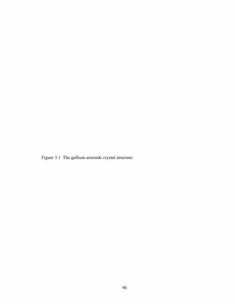
96
Figure 3.1 The gallium arsenide crystal structure.

97
98
Many different etchants and etching techniques have been applied to the GaAs
system [3, 4, 9, 11, 13, 15, 27, 31-39]. Each etchant is applicable for certain situations,
but rarely for all situations. Such a technique would require removal of the
contamination and oxide layers from the surface, while maintaining atomic order. A
methodology that fits these criteria is digital etching.
Digital etching involves the removal of atomic layers of the compound
semiconductor by surface limited reactions (Figure 3.2) [40, 41]. One can imagine this to
be the opposite of epitaxial growth. A well-ordered, clean compound semiconductor can
undergo reactions that will only remove the top layer of atoms. In the example of GaAs,
a surface limited process is conducted to remove the top layer of arsenic, assuming that
the surface is arsenic-terminated. Once this layer is removed, the reaction stops due to its
surface limited nature and the lack of arsenic at the surface. A new etching process is
started to remove the gallium. Again, this reaction is surface limited and stops once all of
the surface gallium atoms are removed. This would provide a method to remove any
defective atomic layers from the compound semiconductor and leave a clean, well-
ordered structure for analysis or further experimentation.
Digital etching is favorable due to the room temperature aspect of the process.
Normal cleaning procedures for GaAs involve thermally desorbing the oxide layers [9,
24, 29, 42]. This produces many different surface structures, depending upon the
temperature reached and time applied [2, 5, 30]. These structures are reconstructions of
the native surface. With thermal desorption techniques, the chances for elemental
desorption of gallium or arsenic increases.

99
Figure 3.2 Digital etching of a compound semiconductor.

100

101
The use of gallium arsenide as a substrate for EC-ALE deposition of another
compound semiconductor is the main goal of this study. A heterojunction could be
formed by electrodepositing a compound semiconductor onto the GaAs substrate.
Cadmium selenide has been deposited on gallium arsenide substrates by co-deposition
methods, as has zinc telluride. [43-46].
To facilitate this deposition, the substrate must be clean and well-ordered. UHV
techniques, such as annealing, thermal desorption, and ion bombardment, are undesirable
for this study. If the GaAs is to be used as a substrate for aqueous solution
electrodeposition, a scheme must be derived that involves simple, chemical etching
techniques to clean the surface of the electrode, without disrupting the periodicity and
stoichiometry of the atoms.
A simple electrochemically-assisted etching technique would allow the GaAs
substrate to be cleaned in an electrochemical-flow deposition system. The etchants could
be passed through the flow-cell that houses the substrate removing any contaminants,
oxides, or damaged layers. This would prepare the substrate for the electrodeposition of
a compound semiconductor by EC-ALE. Since potential control would not be lost and
the cell would never be in contact with atmospheric conditions, the GaAs should remain
clean and oxide free throughout the etching and deposition procedures.
This study investigated the preliminary preparation procedure for GaAs single
crystal wafers, to be used as substrates in an EC-ALE process. UHV-EC methods were
utilized to analyze the surface composition and structure of the GaAs surfaces during
several different etching schemes.

102
Experimental
Two types of GaAs samples were used in the studies presented here: GaAs (100)
wafers and (111) wafers (Atramet, Inc.). Both wafers were doped n-type, with the (100)
wafers being doped with Te at an average concentration of 3 x 1018 cm-3 and the (111)
wafers doped with Te at an average concentration of 1-5 x 1018 cm-3.
The samples were cut into pieces with dimensions approximately 1 cm by 3 cm.
These rectangular samples were mounted into a sample holder consisting of a stainless-
steel puck with molybdenum bars suspended from the bottom of the puck (Figure 3.3). A
stripe of indium metal soldered to the unpolished, backside of the sample acted as an
ohmic contact. This stripe was covered with a piece of platinum foil to help provide
electrical and thermal contact to the sample. The foil-covered GaAs was sandwiched
between the Mo-bars by 008 bolts and nuts. These bars were suspended from the puck
by tungsten wires, which acted as both the electrical contacts, and the heating elements
for any annealing or thermal desorption studies.
The experimental studies presented here utilize ultra-high vacuum
electrochemical (UHV-EC) methods [47]. The UHV surface analysis instrument was
coupled to a stainless steel antechamber that housed an electrochemical cell. This
antechamber was isolated from the main surface analysis chamber by a gate valve. This
allowed the chamber to be backfilled with ultra-pure argon before the electrochemical
experiment, preventing the sample from being contaminated by exposure to the
atmosphere.

103
Figure 3.3 GaAs sample holder.

104

105
The UHV instrument was equipped with a cylindrical mirror analyzer (CMA) for
Auger electron spectroscopy (AES) (Physical Electronics), electron optics for low-energy
electron diffraction (LEED) (Princeton Electronics), an ion gun for sample cleaning by
ion bombardment (Physical Electronics), and a mass analyzer for residual gas analysis
(UTI). The main chamber was ion-pumped with a backing cryo-pump. The cryo-pump
was also used to evacuate the electrochemical antechamber after the experimentation.
The cryo-pump was used due to its high pumping speed for water vapor. Since most of
the pumping load for the chamber was water vapor from the aqueous solutions in the
electrochemical experiment, this pump provided excellent pumping characteristics. The
base pressure of the UHV system was in the range of 10-9 Torr. The background gas
consisted mainly of the water vapor from the aqueous solutions and Ar gas from
backfilling the antechamber. Both gases are inert with respect to the substrates used in
these studies and did not interfere with the experimentation.
During the electrochemical experiment, potentials were measured versus a
Ag/AgCl (3M NaCl) reference electrode (BAS). The auxiliary electrode consisted of a
simple gold wire (Wilkinson Company). Potentials were applied to the working
electrode through an in-house built potentiostat based on op-amp circuitry.
The electrochemical apparatus consisted of a Pyrex H-cell housed in a stainless
steel cylinder, which allows the cell to be purged with Ar before the electrochemical
experiment. The sample was introduced to the antechamber, and the antechamber was
isolated from the main chamber and then backfilled to atmospheric pressure with ultra-
pure Ar gas. The electrochemical cell was introduced into the antechamber through a gate
valve located at the bottom of the chamber. Solutions were fed to the cell through

106
pressurized bottle reservoirs. Three-way stopcocks on the bottles allowed the solutions to
be flowed into the cell and subsequently drained into a waste receptacle.
After the electrochemical experiment, the H-cell was withdrawn from the
antechamber, the gate valve was closed, and the antechamber was evacuated. Once
UHV-level pressures are reached, the sample was transferred into the main chamber for
surface analysis. AES spectra were collected for the polished side of the GaAs crystal
with a 3 KeV ionizing beam. LEED patterns were collected for the polished face of the
crystal and recorded with a Kodak digital camera (Model DC290).
All solutions used in these experiments were prepared with technical-grade or
better chemicals. Ultra-pure water (18 MΩ) from a nanopure system (Barnstead), fed
from the house distilled water line, was used to prepare all the solutions. Before the
solutions were used in the electrochemical experiments, each was purged with ultra-pure
Ar to remove any dissolved oxygen. This prevented not only sample oxidation but also
voltammetry degradation from oxygen reduction.
Results and Discussion
The scope of these experiments is to be able to produce a clean, well-ordered
GaAs surface through chemical or electrochemical surface treatments. Several etching
techniques were applied to the crystal before introduction to the system. These
procedures were mainly wet chemical treatments applied to the crystal without
electrochemical control or manipulation. Other processes were investigated after the
crystal was introduced to the UHV chamber. These methods were usually
electrochemical cyclic voltammetry in aqueous solutions. Surface composition and
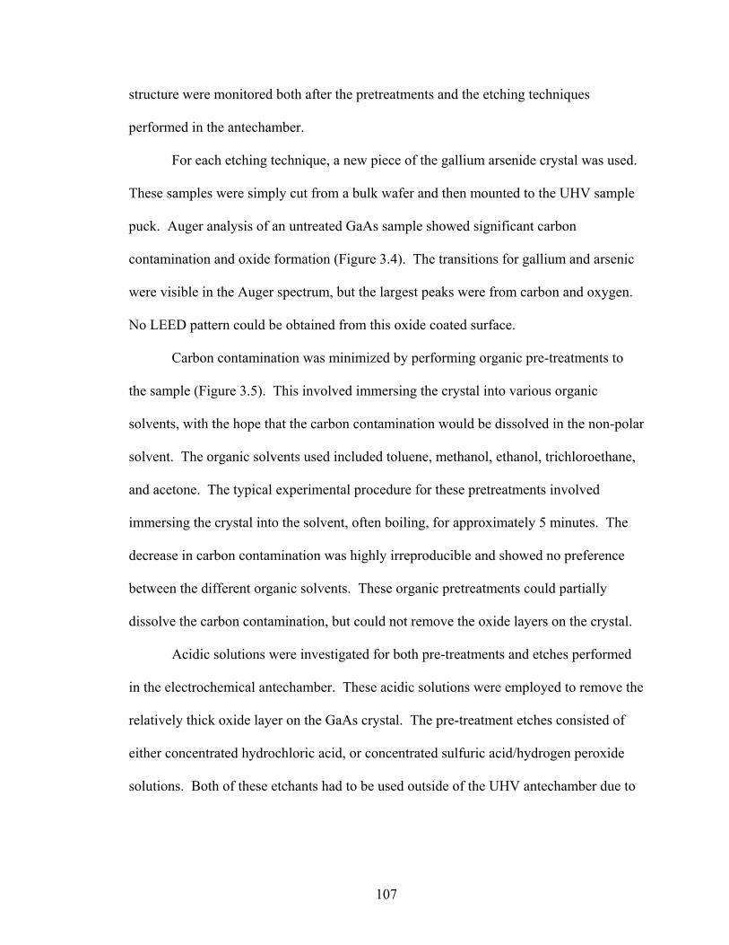
107
structure were monitored both after the pretreatments and the etching techniques
performed in the antechamber.
For each etching technique, a new piece of the gallium arsenide crystal was used.
These samples were simply cut from a bulk wafer and then mounted to the UHV sample
puck. Auger analysis of an untreated GaAs sample showed significant carbon
contamination and oxide formation (Figure 3.4). The transitions for gallium and arsenic
were visible in the Auger spectrum, but the largest peaks were from carbon and oxygen.
No LEED pattern could be obtained from this oxide coated surface.
Carbon contamination was minimized by performing organic pre-treatments to
the sample (Figure 3.5). This involved immersing the crystal into various organic
solvents, with the hope that the carbon contamination would be dissolved in the non-polar
solvent. The organic solvents used included toluene, methanol, ethanol, trichloroethane,
and acetone. The typical experimental procedure for these pretreatments involved
immersing the crystal into the solvent, often boiling, for approximately 5 minutes. The
decrease in carbon contamination was highly irreproducible and showed no preference
between the different organic solvents. These organic pretreatments could partially
dissolve the carbon contamination, but could not remove the oxide layers on the crystal.
Acidic solutions were investigated for both pre-treatments and etches performed
in the electrochemical antechamber. These acidic solutions were employed to remove the
relatively thick oxide layer on the GaAs crystal. The pre-treatment etches consisted of
either concentrated hydrochloric acid, or concentrated sulfuric acid/hydrogen peroxide
solutions. Both of these etchants had to be used outside of the UHV antechamber due to

108
Figure 3.4 Auger spectrum of non-treated GaAs.

109

110
Figure 3.5 Auger spectrum of an acetone and methanol treated GaAs sample.

111

112
their high concentrations. If these concentrated solutions had been introduced to the
antechamber, contamination of the chamber would have occurred.
Both acidic solutions produced similar surfaces. The hydrochloric acid solution
was concentrated (12 M), technical grade HCl. After the crystal was degreased by
organic solvents and rinsed with 18 MΩ water, it was immersed in the concentrated HCl
for 30 seconds. The crystal was then rinsed with 18 MΩ water for 3 minutes. Auger
spectroscopy revealed a surface with a reduced oxide coverage, but the carbon
contamination was significantly higher than after the organic solvent degreasing (Figure
3.6). Chlorine was also present on the surface due to the HCl etchant. The surface
carbon could be attributed to the technical grade acid. LEED analysis of this surface
produced no visible LEED pattern indicating that the surface was not ordered, due to the
carbon contamination disrupting the LEED process.
The sulfuric acid solution consisted of a combination of H2SO4:H2O2:H2O with a
volume ratio of 5:1:1. The sulfuric acid used was concentrated (18 M) technical grade,
and the hydrogen peroxide was 30% in water. This solution was prepared fresh due to
the short life of the hydrogen peroxide. Various etching times were investigated with this
solution. Optimal results occurred at longer etching times; up to 10 minutes. The GaAs
surface oxide layer was again reduced by the acid etchant, but carbon contamination also
increased (Figure 3.7). Sulfur was also present in the Auger spectrum. The small amount
of remaining oxygen in the Auger spectrum could arise from either adsorbed sulfate ions
on the surface, or from a GaAs oxide layer. No LEED pattern was observed for the
crystal etched by this solution.

113
Figure 3.6 Auger spectrum of a HCl etched GaAs sample.

114
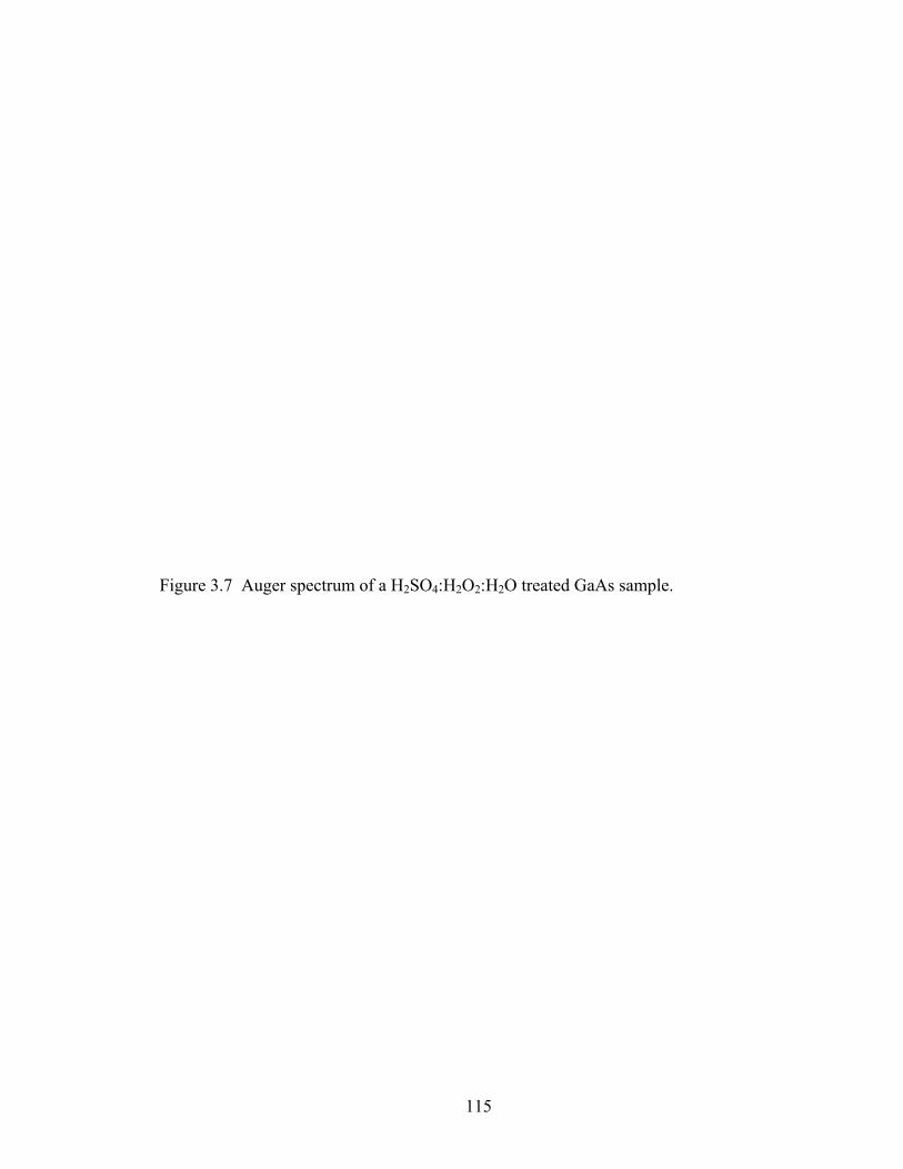
115
Figure 3.7 Auger spectrum of a H2SO4:H2O2:H2O treated GaAs sample.

116
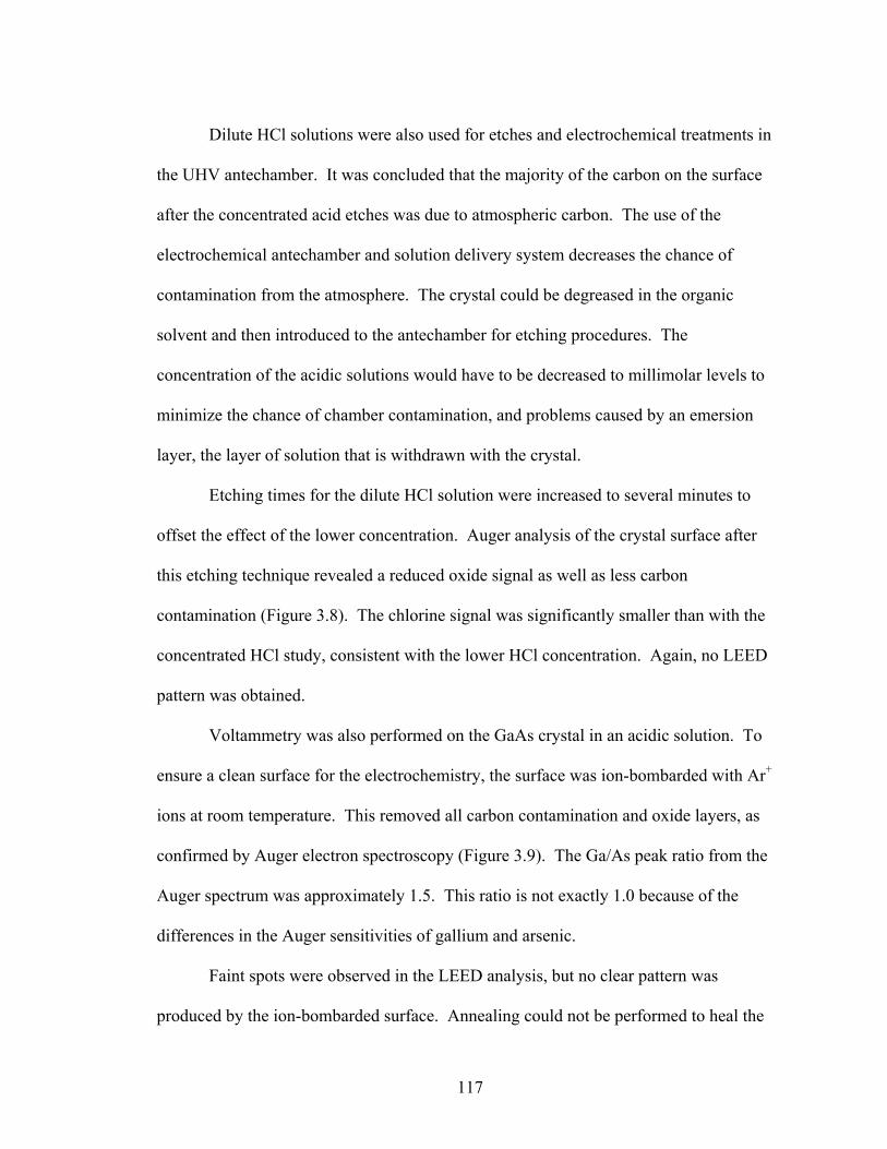
117
Dilute HCl solutions were also used for etches and electrochemical treatments in
the UHV antechamber. It was concluded that the majority of the carbon on the surface
after the concentrated acid etches was due to atmospheric carbon. The use of the
electrochemical antechamber and solution delivery system decreases the chance of
contamination from the atmosphere. The crystal could be degreased in the organic
solvent and then introduced to the antechamber for etching procedures. The
concentration of the acidic solutions would have to be decreased to millimolar levels to
minimize the chance of chamber contamination, and problems caused by an emersion
layer, the layer of solution that is withdrawn with the crystal.
Etching times for the dilute HCl solution were increased to several minutes to
offset the effect of the lower concentration. Auger analysis of the crystal surface after
this etching technique revealed a reduced oxide signal as well as less carbon
contamination (Figure 3.8). The chlorine signal was significantly smaller than with the
concentrated HCl study, consistent with the lower HCl concentration. Again, no LEED
pattern was obtained.
Voltammetry was also performed on the GaAs crystal in an acidic solution. To
ensure a clean surface for the electrochemistry, the surface was ion-bombarded with Ar+
ions at room temperature. This removed all carbon contamination and oxide layers, as
confirmed by Auger electron spectroscopy (Figure 3.9). The Ga/As peak ratio from the
Auger spectrum was approximately 1.5. This ratio is not exactly 1.0 because of the
differences in the Auger sensitivities of gallium and arsenic.
Faint spots were observed in the LEED analysis, but no clear pattern was
produced by the ion-bombarded surface. Annealing could not be performed to heal the

118
Figure 3.8 Auger spectrum of a dilute HCl etched GaAs surface.

119

120
Figure 3.9 Auger spectrum of ion-bombarded GaAs.

121

122
surface damage caused by the ion-bombardment due to the differential thermal
desorption coefficients of the gallium and arsenic.
After confirmation of the cleanliness of the GaAs surface, the crystal was
transferred to the antechamber for electrochemical experimentation. The GaAs was
immersed into a 10 mM HCl solution (Figure 3.10). The potential was scanned
positively from the equilibrium potential, -0.40 V. An oxidation feature appears in the
voltammetry at approximately -0.10 V. This feature was not present in subsequent scans.
The oxidation process responsible for this feature was assumed to be gallium oxidizing
from the surface. The crystal was emmersed from the solution at the equilibrium
potential, -0.40 V.
The Auger spectrum revealed carbon, oxygen, and chlorine present on the surface
(Figure 3.11). The Ga/As Auger peak ratio decreased to approximately 0.96. This
confirms that the oxidation process observed in the voltammetry was gallium oxidation.
This gallium stripping appears to be limited to the first few layers of the surface because
the oxidation was not observed in subsequent scans. No LEED pattern was observed for
this surface.
Coulometry suggested the amount of gallium removed corresponded to about 3
monolayers. Although this was more gallium than desired, the gallium stripping was
encouraging and fit with a digital etching scheme.
Once a method for gallium removal was developed, a suitable procedure for
arsenic stripping was needed. Studies of the EC-ALE deposition of InAs used arsenic
solutions with acetate and perchlorate supporting electrolytes [48]. A blank solution

123
Figure 3.10 Cyclic voltammogram of GaAs (100) in a 10 mM HCl solution.

124

125
Figure 3.11 Auger spectrum of HCl treated GaAs (100).

126

127
consisting of 50 mM NaC2H3O2 and 0.10 M NaClO4 was prepared to investigate
stripping of arsenic from the GaAs single crystal.
The sample was ion-bombarded to remove any contaminations and transferred
into the antechamber for cyclic voltammetry studies. The crystal was immersed in the
acetate solution, producing an equilibrium potential of -0.45 V. The potential was
scanned positively from the equilibrium potential (Figure 3.12). A reproducible
oxidation feature was apparent at 0.20 V. The potential was reversed at 0.40 V and was
scanned negatively to -0.90 V. On the subsequent positive scan, the current increased,
instead of decreasing, as would generally be expected with a reverse in the scan direction.
This increase in reductive current continued until the potential reached approximately -
0.65 V, when the current dropped to zero. This reductive current was thought to be the
stripping of arsenic from the surface. The potential was scanned until the equilibrium
potential of -0.45 V was reached, where the crystal was emmersed from the solution and
transferred into the main chamber of the UHV system for surface analysis.
The Auger spectrum for this surface contained a large oxygen signal and little
carbon contamination (Figure 3.13). The Ga/As Auger peak ratio was 4.48. This agrees
with the theory that the reductive current observed in the voltammetry was due to
stripping of arsenic from the GaAs crystal. The oxygen present on the surface may have
been from the electrolytes, acetate or perchlorate, but was most likely an oxide layer
formed when the gallium-rich surface was emmersed from the cell. Due to the large
oxygen surface content, no LEED pattern was observed. Coulometry used to determine
the amount of arsenic stripped during the scan suggested removal of approximately 8
monolayers. Again, this amount was more
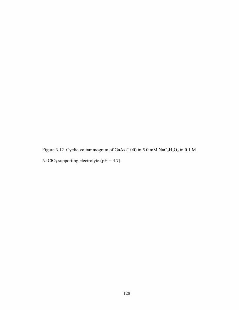
128
Figure 3.12 Cyclic voltammogram of GaAs (100) in 5.0 mM NaC2H3O2 in 0.1 M
NaClO4 supporting electrolyte (pH = 4.7).

129

130
Figure 3.13 Auger spectrum of acetate treated GaAs (100).
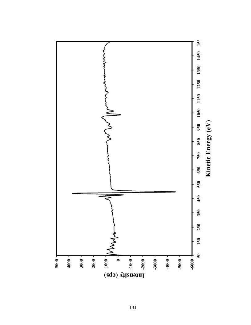
131
132
than the desired 1 monolayer of arsenic, but it provided a method for removing arsenic
from the gallium arsenide surface.
To further investigate a possible digital etching scheme for gallium arsenide,
better pre-treatments were needed. Tereschenko and researchers developed a solution of
HCl in 2-propanol that could be used to etch GaAs [38, 39, 42]. This solution was used
to etch a GaAs (100) crystal prior to its introduction into a UHV system. The HCl in the
2-propanol solution was prepared with reagent-grade HCl and HPLC grade 2-propanol.
The concentration of the HCl was 3.0 M. The GaAs crystal was mounted and then
prepared for the surface treatment. Degreasing was performed by immersing the crystal
in boiling toluene for 5 minutes. The crystal was washed with 18 MΩ water and then
blown dry with nitrogen. The crystal was then etched with a H2SO4:H2O2:H2O (20:1:1
volume ratio) solution at approximately 40 °C for 20 seconds. The crystal was again
washed with 18 MΩ water and blown dry with nitrogen. The final etch with the HCl/2-
propanol solution was applied to the crystal for 2 minutes. The crystal was washed with
2-propanol and blown dry before introduction into the UHV system.
Auger analysis showed a surface with slight carbon and oxygen contaminations,
but the overall cleanliness was vastly improved over other techniques (Figure 3.14). The
Ga/As ratio Auger peak ratio was 1.4, which is in very good agreement with the ion-
bombarded surface ratio. A sharp (1 x 1) LEED pattern was obtained indicating that the
surface was highly ordered and the contamination was not disrupting the periodicity of
the surface (Figure 3.15). This technique gave a method to prepare a reproducible clean,
well-ordered GaAs (100) surface for further studies.

133
Figure 3.14 Auger spectrum of 2-propanol/HCl treated GaAs (100).

134

135
Figure 3.15 LEED pattern of 2-propanol/HCl treated GaAs (100).

136

137
Conclusions
Several etching techniques were conducted for the purpose of producing a clean,
well-ordered GaAs surface. A procedure was needed to produce this surface so the GaAs
could be further used as a substrate for EC-ALE deposition. A digital etching approach
was used as a model for the preparation of this surface.
Concentrated acidic etches used on the GaAs crystal removed the oxide layers
from the surface, but could not dissolve the carbonaceous contaminations. Concentrated
HCl solutions and H2SO4:H2O2:H2O solutions were investigated.
Dilute HCl solutions were applied to the crystal in the UHV electrochemical
antechamber. These experiments were performed at open-circuit, with no potential
control. This etchant showed improvement from the concentrated etches, due to the
isolation capabilities of the antechamber. Both oxygen and carbon were decreased.
Stripping of gallium was achieved by cyclic voltammetry in a 10 mM HCl
solution. An oxidative feature in the voltammetry was observed for the first cycle, but
not in any subsequent cycles. This feature was attributed to gallium oxidative stripping.
Approximately 3 monolayers of gallium were stripped from the electrode. No LEED
pattern was obtained.
Arsenic was reductively stripped from the crystal by cyclic voltammetry in an
acetate/perchlorate solution. Approximately 8 monolayers of arsenic were stripped from
the crystal. No surface limited stripping feature could be found in the voltammetry, but a
means of removing arsenic from the electrode’s surface was realized. No LEED pattern
was obtained, due to the large amount of oxygen on the surface.

138
A pre-treatment procedure was conducted according to a literature report. This
treatment involved reacting the GaAs crystal with a solution of HCl in 2-propanol. In
this etch, a GaAs surface with reduced carbon and oxygen contamination was obtained.
A clean (1 x 1) LEED pattern was produced by the treated surface, establishing a
procedure for cleaning the GaAs crystal without disrupting the surface order or
stoichiometry.
These studies have provided a starting point for the development of a digital
etching scheme for gallium arsenide. This digital etching process will provide a method
for preparing GaAs surfaces for use as substrates for the EC-ALE process. This would
result in the fabrication of a heterojunction of two compound semiconductors by
chemical/electrochemical methods. Further studies need to be conducted to fully
construct this digital etching procedure and to facilitate heterojunction electrodeposition.
Cited References
1. J. R. Arthur, Surf. Sci., 1974, 43, p. 449.
2. D. J. Chadi, C. Tanner, and J. Ihm, Surf. Sci., 1982, 120, p. L425.
3. I. Ivanov, A. Mazur, and J. Pollman, Surf. Sci., 1980, 92, p. 365.
4. Y. Ke, S. Milano, X. W. Wang, N. Tao, and Y. Darici, Surf. Sci., 1998, 415, p. 29.
5. P. K. Larsen and G. Meyer-Ehmsen, Surf. Sci., 1990, 240, p. 168.
6. M. A. Mendez, F. J. Palomares, M. T. Cuberes, M. L. Gonzalez, and F. Soria,
Surf. Sci., 1991, 251/252, p. 145.

139
7. I. Shiota, K. Motoya, T. Ohmi, N. Miyamoto, and J. Nishizawa, J. Electrochem.
Soc., 1977, 124, (1), p. 155.
8. J. T. Wolan, W. S. Epling, and G. B. Hoflund, J. Appl. Phys., 1997, 81, (9), p.
6160.
9. J. L. Zilko and R. S. Williams, J. Electrochem. Soc., 1982, 129, (2), p. 406.
10. G. Scherb, A. Kazimirov, J. Zegenhagen, T. Schultz, R. I. Feidenhans, and B. O.
Fimland, Appl. Phys. Lett., 1997, 71, (20), p. 2990.
11. A. Etcheberry, B. Fotouhi, D. Ballutaud, M. I'Haridon, D. Moutonnet, and J. L.
Sculfort, J. Electrochem. Soc., 1991, 138, (9), p. 2802.
12. R. Schlesinger and P. J. Janietz, J. Electrochem. Soc., 1992, 139, (7), p. 1936.
13. S. Lingier and W. P. Gomes, Ber. Buns. Phys. Chem., 1991, 95, (2), p. 170.
14. K. Akita, Y. Sugimoto, and H. Kawanishi, J. Electrochem. Soc., 1991, 138, (7), p.
2095.
15. H. F. Hsieh and H. C. Shih, J. Electrochem. Soc., 1991, 138, (7), p. 1965.
16. T. M. Valahas, J. S. Sochanski, and H. C. Gatos, Surf. Sci., 1971, 26, p. 41.
17. L. G. Casagrande, A. Juang, and N. L. Lewis, J. Phys. Chem. B, 2000, 104, p.
5436.
18. H. Booyens, J. H. Basson, A. W. R. Leitch, M. E. Lee, and C. M. Stander, Surf.
Sci., 1983, 130, p. 259.

140
19. N. Bundgens, H. Luth, M. Mattern-Klosson, A. Spitzer, and A. Tulke, Surf. Sci.,
1985, 160, p. 46.
20. J. H. Dinan, L. K. Galbraith, and T. E. Fischer, Surf. Sci., 1971, 26, p. 587.
21. P. Mark, P. Pianetta, I. Lindau, and W. E. Spicer, Surf. Sci., 1977, 69, p. 735.
22. F. Meyer and A. Kroes, Surf. Sci., 1975, 47, p. 124.
23. P. Pianetta, I. Lindau, P. E. Gregory, C. M. Garner, and W. E. Spicer, Surf. Sci.,
1978, 72, p. 298.
24. H. J. Yoon, M. H. Choi, and I. S. Park, J. Electrochem. Soc., 1992, 139, (11), p.
3229.
25. R. Morton, S. S. Lau, D. B. Poker, P. K. Chu, K. K. Fung, and N. Wang, J. Appl.
Phys., 1998, 84, (9), p. 4929.
26. M. C. G. Passeggi, R. R. Koropecki, J. Ferron, B. Molinas, and G. M. Guadalupi,
Surf. Coat. Tech., 1999, 122, p. 56.
27. K. Jacobi, G. Steinert, and W. Ranke, Surf. Sci., 1976, 57, p. 571.
28. A. U. Mac Rae, Surf. Sci., 1966, 4, p. 247.
29. P. Moriaty, P. H. Beton, Y. R. Ma, A. W. Dunn, M. Henini, and D. A. Woolf, J.
Vac. Sci. Tech. B, 1996, 14, (2), p. 943.
30. C. W. Snyder, J. Sudijono, C. H. Lam, M. D. Johnson, and B. G. Orr, Phys. Rev.
B, 1994, 50, p. 18194.
141
31. C. C. Chang, P. H. Citrin, and B. Schwartz, J. Vac. Sci. Tech., 1977, 14, (4), p.
943.
32. G. C. DeSalvo, C. A. Bozada, J. L. Ebel, D. C. Look, J. P. Barette, C. L. A.
Cerny, R. W. Dettmer, J. K. Gillespie, C. K. Havasy, T. J. Jenkins, K. Nakano, C.
I. Pettiford, T. K. Quach, J. S. Sewell, and G. D. Via, J. Electrochem. Soc., 1996,
143, (11), p. 3652.
33. P. Drathen, W. Ranke, and K. Jacobi, Surf. Sci., 1978, 77, p. L162.
34. A. Kahn, G. Cisneros, M. Bonn, and P. Mark, Surf. Sci., 1978, 71, p. 387.
35. Z. H. Lu, C. Lagarde, E. Sacher, J. F. Currie, and A. Yelon, J. Vac. Sci. Tech. A,
1989, 7, (3), p. 646.
36. T. Meguro and Y. Aoyagi, Appl. Surf. Sci., 1997, 112, p. 55.
37. X. S. Wang, K. W. Self, R. Maboudian, C. Huang, V. Bressler-Hill, and W. H.
Weinberg, J. Vac. Sci. Tech. A, 1993, 11, (4), p. 1089.
38. O. E. Tereshchenko, A. S. Terekhov, D. Paget, P. Chiaradia, J. E. Bonnet, R.
Belkhou, and A. Taleb-Ibrahimi, Surf. Sci., 2002, 507-510, p. 411.
39. O. E. Tereshchenko, S. I. Chikichev, and A. S. Terekhov, Appl. Surf. Sci., 1999,
142, p. 75.
40. T. A. Sorenson, B. K. Wilmer, and J. L. Stickney, in Solid-Liquid
Electrochemical Interfaces, 1997, American Chemical Society: Washington, p.
115-125.
142
41. Q. P. Lei and J. L. Stickney, Mat. Res. Soc. Symp. Proc., 1992, 237, p. 335.
42. O. E. Tereshchenko, S. I. Chikichev, and A. S. Terekhov, J. Vac. Sci. Tech. A,
1999, 17, (5), p. 2655.
43. L. Beaunier, H. Cachet, M. Froment, and G. Maurin, J. Electrochem. Soc., 2000,
147, (5), p. 1835.
44. L. Beaunier, H. Cachet, R. Cortes, M. Froment, and A. Etcheberry, Thin Solid
Films, 2001, 387, p. 108.
45. H. Cachet, R. Cortes, M. Froment, and G. Maurin, Phil. Mag. Lett., 1999, 79,
(10), p. 837.
46. B. Bozzini, C. Lenardi, and N. Lovergine, Matr. Chem. Phys., 2000, 66, p. 219.
47. M. P. Soriaga and J. L. Stickney, in Modern Techniques in Electroanalysis, ed. P.
Vanysek, John Wiley & Sons, 1996, p. 1.
48. T. L. Wade, R. Vaidyanathan, U. Happek, and J. L. Stickney, J. Electroanal.
Chem., 2001, 500, p. 322.

143
Chapter 4
CONCLUSIONS AND FUTURE STUDIES

144
Conclusions
Electrodeposition of Antimony on Copper
The underpotential deposition of antimony from acidic chloride solutions onto the
low-index planes of copper was investigated by ultra-high vacuum electrochemistry
methods. Atomic layers of chlorine were originally formed on the copper substrate upon
immersion into the antimony solution. The Cl structures, (√3x√3)R30° on Cu(111),
(√2x√2)R45° on Cu(100), and c(2x2) on Cu(110), agreed with literature values. These Cl
layers remained on the substrate until the onset of Sb deposition. Once the Sb began to
deposit at approximately -0.200 V, combination structures, containing both Sb and Cl
formed on the copper substrate surfaces.
As the potential was scanned to more negative values, more Sb deposited onto the
electrode, displacing Cl atoms. The Sb adlayer on the Cu(111) formed a (√3x√3)R30°
structure with a small amount of Cl still present. At a deposition potential of -0.350 V,
the Cl coverage dropped to nearly zero and the Sb coverage was approximately 0.75.
This new Sb coverage produced a LEED pattern consistent with a (3x√21) unit cell. The
basis for this unit cell could not be determined, and STM data is needed to fully
characterize this Sb structure.
The Cu(100) demonstrated a Cl-Sb transition structure, (2√2x√2)R45°, before a
(3x2) unit cell at was formed at a deposition potential of -0.350 V. This structure gave an
Sb coverage of 0.5 and a Cl coverage of 0.25. The ideal Sb coverage for this unit cell is
0.33. The reason for the discrepancy in the Sb coverages and the presence of Cl on the
surface could not be determined with these techniques. This gives another area where
STM data is needed to fully understand the system.

145
The matrix denoted structure,
− 11
31, for the Cl-Sb adlayer on Cu(110)
transformed into a (3x2) structure upon further Sb deposition at –0.400 V. The calculated
coverage and experimental coverage values were approximately equal at 0.67. The
Auger spectral data indicated a small amount, approximately 0.2 ML, of Cl still present at
this potential. How this Cl was incorporated into the electrodeposited adlayer could not
be determined. Beyond –0.450 V, no well-ordered structures were observed, and bulk Sb
deposition began.
These results demonstrated that a surface-limited reaction does occur in the
electrodeposition of Sb onto Cl modified low-index planes of Cu. A sequence of ordered
structures was observed on each of the surfaces. These structures were highly dependent
on the electrolyte, due to the formation of Cl-modified Cu surfaces before the Sb
deposition. A well-defined UPD process does take place, even though it was not present
in the voltammetry.
Surface Manipulation of Gallium Arsenide
Several etching techniques were conducted for the purpose of producing a clean,
well-ordered GaAs surface. A procedure was needed to produce this surface so the GaAs
could be further used as a substrate for EC-ALE deposition. A digital etching approach
was used as a model for the preparation of this surface.
Concentrated acidic etches used on the GaAs crystal removed the oxide layers
from the surface, but could not dissolve the carbonaceous contaminations. Concentrated
HCl solutions and H2SO4:H2O2:H2O solutions were investigated.

146
Dilute HCl solutions were applied to the crystal in the UHV electrochemical
antechamber. These experiments were performed at open-circuit, with no potential
control. This etchant showed improvement from the concentrated etches, due to the
isolation capabilities of the antechamber. Both oxygen and carbon were decreased.
Stripping of gallium was achieved by cyclic voltammetry in a 10 mM HCl
solution. An oxidative feature in the voltammetry was observed for the first cycle, but
not in any subsequent cycles. This feature was attributed to gallium oxidative stripping.
Approximately 3 monolayers of gallium were stripped from the electrode. No LEED
pattern was obtained.
Arsenic was reductively stripped from the crystal by cyclic voltammetry in an
acetate/perchlorate solution. Approximately 8 monolayers of arsenic were stripped from
the crystal. No surface limited stripping feature could be found in the voltammetry, but a
means of removing arsenic from the electrode’s surface was realized. No LEED pattern
was obtained, due to the large amount of oxygen on the surface.
A pre-treatment procedure was conducted according to a literature report. This
treatment involved reacting the GaAs crystal with a solution of HCl in 2-propanol. In
this etch a GaAs surface with reduced carbon and oxygen contamination was obtained. A
clean (1 x 1) LEED pattern was produced by the treated surface, establishing a procedure
for cleaning the GaAs crystal without disrupting the surface order or stoichiometry.
These studies have provided an initial set of data for the development of a digital
etching scheme for gallium arsenide. This process will provide a method for preparing
GaAs surfaces for use as substrates for the EC-ALE process. This would result in the

147
fabrication of a heterojunction of two compound semiconductors by chemical-
electrochemical methods.
Future Studies
Electrodeposition of Antimony on Copper
The investigation of antimony electrodeposition on copper electrodes was
conducted to help improve the EC-ALE process for the deposition of antimony
containing compound semiconductors, such as InSb. Indium deposition on the low-index
planes of copper from acidic chloride solutions was conducted, but no distinct structures
were discovered. Auger spectral data indicate significant levels of oxygen present after
indium deposition. This oxygen disrupted the LEED analysis yielding no clear, well-
ordered structure for the In.
Since the In was not depositing ordered structures, Sb layers were
electrodeposited to attempt to form an InSb ordered structure. Two experimental
procedures were carried out. First, an Sb adlayer was deposited onto the copper
electrode, and then In was electrodeposited onto this Sb-modified surface. This resulted
in no well-ordered LEED pattern. Significant oxygen levels were detected in the Auger
spectrum.
The second procedure involved electrodepositing Sb onto an In-modified copper
electrode. No UPD-like feature was apparent in the voltammetry. Auger analysis of this
adlayer indicated not only In and Sb present on the surface, but also Cl and O. This
experiment did not produce an ordered LEED pattern.
148
Further experiments with this system need to be conducted to form a well-ordered
InSb adlayer on the copper electrode. InSb and InAs have been formed on both copper
and gold electrodes by EC-ALE methods, but the individual deposition processes have
not been fully examined [1, 2]. Further investigation of the electrolyte content of the
indium solution may elucidate a scheme to deposit an adlayer of oxide-free In. Other
electrolytes may be investigated for the Sb deposition as well. The presence of the
chlorine during the antimony deposition should be examined. While the chlorine seemed
to not interfere with the Sb deposition, this electrolyte could have disrupted the In
deposition process.
Surface Manipulation of Gallium Arsenide
The electrochemical and etching data obtained for the surface preparation of
GaAs, provides an initial set of data for this process. While significant progress was
made, these studies were very preliminary. Further investigation on etchant and
electrochemical solutions need to be made.
Electrochemical etching, such as the gallium etching by aqueous HCl, needs to be
performed after the 2-propanol/HCl etching. This would not only help validate the
effectiveness of the propanol etch, but also provide further data for the electrochemical
etching. Gallium electrochemical etching followed by arsenic electrochemical etching
would effectively remove several monolayers of the GaAs single crystal. Further
electrochemical experimentation needs to be conducted to attempt to lower the amount of
material removed for each electrochemical cycle.

149
This data is a good preliminary study on the surface manipulation of gallium
arsenide single crystals. Once this procedure is perfected, these GaAs single crystals can
be used for EC-ALE substrates. This would provide a lattice matched substrate for other
compound semiconductors, such as ZnSe. If ZnSe could be electrodeposited onto a
GaAs substrate, this would construct a semiconductor heterojunction that was completely
formed by electrochemical or wet-chemical methods. ZnSe and ZnTe have been
electrodeposited onto InP and GaAs substrates using a co-deposition method, but this
does not give the epitaxial control that an EC-ALE process exhibits [3-5]. The
construction of this type of material would open new and exciting areas for the
electrochemical deposition of compound semiconductors.
Cited References
1. T. L. Wade, R. Vaidynathan, U. Happek, and J. L. Stickney, J. Electroanal. Chem., 2001, 322, p. 11. 2. T. L. Wade, L. C. Ward, C. B. Maddox, U. Happek, and J. L. Stickney, Electrochem. Sol. State Lett., 1999, 2, p. 616. 3. L. Beaunier, H. Cachet, R. Cortes, M. Froment, and A. Etcheberry, Thin Solid Films, 2001, 387, p. 108. 4. B. Bozzini, C. Lenardi, and N. Lovergine, Mater. Chem. Phys., 2000, 66, p. 219. 5. L. Beaunier, H. Cachet, M. Froment, and G. Maurin, J. Electrochem. Soc., 2000, 147, (5), p. 1835.
Related Documents


