Surface enhanced Raman spectroscopy as a probe for local modification of carbon films A. Ilie,* C. Durkan, W. I. Milne, and M. E. Welland Engineering Department, Cambridge University, Cambridge CB2 1PZ, United Kingdom Received July 13, 2001; revised manuscript received 25 February 2002; published 25 July 2002 The possibility of achieving nanometer-scale sensitivity in a surface-enhanced Raman SERS experiment while using larger-sized probes 0.1–1 m is investigated. The application targeted is carbon film transfor- mation under high-energy beam irradiation, and, primarily, the transformation of amorphous carbon into nanocrystalline graphite. The carbon film covers nanometer-size Ag particles which enhance the signal from zones of material adjacent to them. This geometry gives access to the film/substrate interface, and in this way it complements scanning near-field techniques which have similar spatial sensitivity but are mainly surface sensitive. The SERS effect has been studied as a function of the Ag nanoparticle size, carbon film thickness, and excitation wavelength. A selective enhancement of the Raman cross section of the D band of amorphous carbons was observed. The dielectric properties of the carbon film, when used as an overlayer, strongly affect the SERS enhancement, so that changes in the dielectric function upon irradiation can be used to produce local enhancement contrast, and to establish an identification procedure for material transformation. DOI: 10.1103/PhysRevB.66.045412 PACS numbers: 78.30.Ly, 81.05.Uw, 81.07.b, 81.40.Tv I. INTRODUCTION There is increasing interest in producing carbon materials with a structure that varies on the nanometer scale. These will take advantage of the unique property of carbon that, solely by varying the type of bonding, very different local properties can be obtained, ranging from diamond to gra- phitelike or nanotubelike. The applications of these materials can be various, such as large area electron-field emitters, 1–6 or, at the other end of the spectrum, as antifuses 7 and nan- odevices in nanotechnology. Various deposition techniques allow the direct manufac- ture of thin films with mixed sp 2 and sp 3 phases. 1–6 How- ever, the spatial distribution of the two phases is random in these cases, while for the applications mentioned above it is desirable to be able to controllably induce a nanostructure of a specific type and at predetermined locations. One way to achieve this goal is to use high-energy ion or electron beams to locally transform a given matrix. In this way, graphitic regions can be formed in a diamondlike matrix, 8 or fullerenes in amorphous carbon or graphitic materials, 9 or, conversely, graphitic materials, such as fullerenes, can be transformed into diamond. 10 Probing the extent of a local transformation is not always easy. Ideally, we would like to use a technique which i has a nanometer scale sensitivity, ii can be tuned to probe vari- ous depths in the film down to the film-substrate interface, and iii provides structural information. Atomic force mi- croscopy AFM can reveal a contrast between irradiated and nonirradiated zones based on their different conductivities; nevertheless, due to the small size of the probed area, this technique is restricted to materials or regions with rather high conductivity ( 10 5 1 cm 1 ), and, in addition, it does not provide direct structural information. Energy-loss- spectroscopy EELS is a powerful structural characteriza- tion technique at the nanometer scale; 11 however, the infor- mation obtained is global, integrated over the film bulk and interfaces. Cross-sectional EELS can alleviate this problem, 12 but it is very difficult to apply to the study of nanometer scale regions embedded in an matrix. Here we focus on the surface enhanced Raman SERS technique, which can potentially satisfy the requirements listed above. Indeed, Raman spectroscopy is the technique of choice for identifying bonding in various carbon systems, 13–18 while its surface-enhanced variant has been used for the detection of low-dimensionality objects, such as single-wall nanotubes 19 and single molecules, 20,21 and for the study of interfacial phenomena and ultrathin films. 22–24 Usu- ally, nm-scale Raman information is obtained using scanning near-field optical microscope SNOM techniques, and to date the highest spatial resolution reported was about 100– 150 nm with aperture-based SNOMs 25,26 and about 50 nm when using an apertureless microscope. 27 We investigated an alternative way to detect nm size ac- tive areas in carbon films of tens of nm thickness, while still using larger-sized Raman probes of 0.1–1 m. This utilizes the selective enhancement of the signal I * from the zone of interest e.g. modified by irradiation in our target application when this is adjacent to Ag nanostructures, so that I * rises above the nonenhanced background I given by the remaining probed area unmodified. When expressed in terms of the respective surfaces, this condition leads to S * R S , where S * and S are the areas of the enhanced and nonenhanced regions, respectively, S * S is the total probed area, and R is the enhancement factor for region S * . For S * S in the range 10 4 – 10 6 nm 2 as for 0.1–1-m diameter probes, an enhancement factor R 10 3 – 10 4 is sufficient to allow the signal from a region S * with a diameter as low as 30 nm to largely dominate the overall signal. We were interested mainly in the configuration with the carbon film grown on top of the Ag nanostructures, in order to probe the effective- ness of the transformation down to the substrate, as required above; this configuration gives complementary information to that from SNOM techniques, which are sensitive mainly to the top surface. We explored the feasibility of this technique primarily in conjunction with tetrahedral amorphous carbon ta-C, the form of amorphous carbon with the highest sp 3 bonding PHYSICAL REVIEW B 66, 045412 2002 0163-1829/2002/664/04541213/$20.00 ©2002 The American Physical Society 66 045412-1

Welcome message from author
This document is posted to help you gain knowledge. Please leave a comment to let me know what you think about it! Share it to your friends and learn new things together.
Transcript
Surface enhanced Raman spectroscopy as a probe for local modification of carbon films
A. Ilie,* C. Durkan, W. I. Milne, and M. E. WellandEngineering Department, Cambridge University, Cambridge CB2 1PZ, United Kingdom
!Received July 13, 2001; revised manuscript received 25 February 2002; published 25 July 2002"
The possibility of achieving nanometer-scale sensitivity in a surface-enhanced Raman !SERS" experimentwhile using larger-sized probes !0.1–1 #m" is investigated. The application targeted is carbon film transfor-mation under high-energy beam irradiation, and, primarily, the transformation of amorphous carbon intonanocrystalline graphite. The carbon film covers nanometer-size Ag particles which enhance the signal fromzones of material adjacent to them. This geometry gives access to the film/substrate interface, and in this wayit complements scanning near-field techniques which have similar spatial sensitivity but are mainly surfacesensitive. The SERS effect has been studied as a function of the Ag nanoparticle size, carbon film thickness,and excitation wavelength. A selective enhancement of the Raman cross section of the D band of amorphouscarbons was observed. The dielectric properties of the carbon film, when used as an overlayer, strongly affectthe SERS enhancement, so that changes in the dielectric function upon irradiation can be used to produce localenhancement contrast, and to establish an identification procedure for material transformation.
DOI: 10.1103/PhysRevB.66.045412 PACS number!s": 78.30.Ly, 81.05.Uw, 81.07.!b, 81.40.Tv
I. INTRODUCTION
There is increasing interest in producing carbon materialswith a structure that varies on the nanometer scale. Thesewill take advantage of the unique property of carbon that,solely by varying the type of bonding, very different localproperties can be obtained, ranging from diamond to gra-phitelike or nanotubelike. The applications of these materialscan be various, such as large area electron-field emitters,1–6or, at the other end of the spectrum, as antifuses7 and nan-odevices in nanotechnology.Various deposition techniques allow the direct manufac-
ture of thin films with mixed sp2 and sp3 phases.1–6 How-ever, the spatial distribution of the two phases is random inthese cases, while for the applications mentioned above it isdesirable to be able to controllably induce a nanostructure ofa specific type and at predetermined locations. One way toachieve this goal is to use high-energy ion or electron beamsto locally transform a given matrix. In this way, graphiticregions can be formed in a diamondlike matrix,8 orfullerenes in amorphous carbon or graphitic materials,9 or,conversely, graphitic materials, such as fullerenes, can betransformed into diamond.10Probing the extent of a local transformation is not always
easy. Ideally, we would like to use a technique which !i" hasa nanometer scale sensitivity, !ii" can be tuned to probe vari-ous depths in the film down to the film-substrate interface,and !iii" provides structural information. Atomic force mi-croscopy !AFM" can reveal a contrast between irradiated andnonirradiated zones based on their different conductivities;nevertheless, due to the small size of the probed area, thistechnique is restricted to materials or regions with ratherhigh conductivity ("10!5 $!1 cm!1), and, in addition, itdoes not provide direct structural information. Energy-loss-spectroscopy !EELS" is a powerful structural characteriza-tion technique at the nanometer scale;11 however, the infor-mation obtained is global, integrated over the film bulk andinterfaces. Cross-sectional EELS can alleviate thisproblem,12 but it is very difficult to apply to the study of
nanometer scale regions embedded in an matrix.Here we focus on the surface enhanced Raman !SERS"
technique, which can potentially satisfy the requirementslisted above. Indeed, Raman spectroscopy is the technique ofchoice for identifying bonding in various carbonsystems,13–18 while its surface-enhanced variant has beenused for the detection of low-dimensionality objects, such assingle-wall nanotubes19 and single molecules,20,21 and for thestudy of interfacial phenomena and ultrathin films.22–24 Usu-ally, nm-scale Raman information is obtained using scanningnear-field optical microscope !SNOM" techniques, and todate the highest spatial resolution reported was about 100–150 nm with aperture-based SNOMs25,26 and about 50 nmwhen using an apertureless microscope.27We investigated an alternative way to detect nm size ac-
tive areas in carbon films of tens of nm thickness, while stillusing larger-sized Raman probes of 0.1–1 #m. This utilizesthe selective enhancement of the signal I* from the zone ofinterest !e.g. modified by irradiation in our target application"when this is adjacent to Ag nanostructures, so that I* risesabove the nonenhanced background I given by the remainingprobed area !unmodified". When expressed in terms of therespective surfaces, this condition leads to S*R"S , whereS* and S are the areas of the enhanced and nonenhancedregions, respectively, S*#S is the total probed area, and R isthe enhancement factor for region S*. For S*#S in therange 104– 106 nm2 !as for 0.1–1-#m diameter probes", anenhancement factor R%103– 104 is sufficient to allow thesignal from a region S* with a diameter as low as 30 nm tolargely dominate the overall signal. We were interestedmainly in the configuration with the carbon film grown ontop of the Ag nanostructures, in order to probe the effective-ness of the transformation down to the substrate, as requiredabove; this configuration gives complementary informationto that from SNOM techniques, which are sensitive mainlyto the top surface.We explored the feasibility of this technique primarily in
conjunction with tetrahedral amorphous carbon !ta-C", theform of amorphous carbon with the highest sp3 bonding
PHYSICAL REVIEW B 66, 045412 !2002"
0163-1829/2002/66!4"/045412!13"/$20.00 ©2002 The American Physical Society66 045412-1
content !&85%".28 ta-C is interesting since, due to the pres-ence of some sp2 bonding, it has a higher propensity fortransformation into a graphitic phase through irradiation orthermal annealing than diamond,8 though retaining manydiamondlike properties. While no irradiation was performedin this study, our aim was to check the prerequisites to per-form such a SERS experiment: whether there is sufficientenhancement for selective nm-scale sensitivity, how the Ra-man spectra change relative to the well-known bulk spectra,and whether there are additional dependencies such as on thecarbon overlayer thickness.We found that the magnitude of the SERS effect varies
with the ta-C overlayer thickness, and with different depen-dencies when changing the excitation wavelength. For amicron-size probe the intensity of the SERS signal increasedby about 103– 104 relative to the normal Raman signal whenincreasing the wavelength to the infrared. This is alreadysufficient enhancement to meet our purpose of selective de-tection using larger size probes. The complex behavior withthe overlayer thickness and excitation wavelength, was dis-cussed by considering two possible competitive effects: !i"tuning into the SERS resonance of the carbon-coated Agnanostructures, an effect related to the dielectric function ofthe carbon film; and !ii" optical interference accompanyingRaman scattering as the carbon film thickness is comparableto the excitation wavelength. The SERS effect is found to behighly sensitive to the interfacial layer of the ta-C film,which is more sp2 rich, but it also extends into the film’sbulk. This high sensitivity is also accompanied by a largerdispersion with energy of the I(D)/I(G) parameter, the ratioof the intensities of the Raman D and G bands, than fornormal Raman scattering in any bulk carbon material. This isthe first report of a selective enhancement of the Raman Dband in amorphous carbons through a surface-enhancedeffect.We also discuss the sensitivity of the SERS effect to
changes in the dielectric properties of the overlayer, as occurin an irradiation experiment. Therefore, amorphous diamond-like and graphitic regions will show a clear enhancementcontrast, despite having features in the same spectral range.This allowed us to set a simple procedure for assessing whenthe local transformation from a diamondlike phase toward agraphitic phase takes place. The SERS technique describedhere can work particularly well for transformations in whichthe final phase has a low imaginary part of the dielectricconstant and Raman features in a different spectral regionthan the initial phase, e.g. amorphous carbon into onions, orfullerenes into diamond.
II. SERS AND SURFACE PLASMONSIN Ag NANOSTRUCTURES
The SERS effect induced by small noble metal particlesappears to be of complex origin. The main volume of datagenerated in the last two decades points, essentially, to anelectromagnetic enhancement with a near-field upper valueof about 107– 108, which is due to the excitation of surfaceplasmon resonances,29 covering the spectral range from vis-ible to near-UV. Only recently, made possible by the devel-
opment of near-field scanning techniques, have some notabledisagreements with this approach been observed. Accord-ingly, very peculiar, individual ‘‘hot’’ particles have beenidentified,20,21 which are responsible for a huge local en-hancement, up to 1014, so that single molecules could bedetected. Recent calculations based on the numerical resolu-tion of the Maxwell’s equations showed that the sharp anglesof particles with irregular shape can generate a near-fieldenhancement locally in excess of 1012, which can be corre-lated with polarization charge distributions.30 Effects otherthan electromagnetic, such as chemical or nonlinear opticaleffects !e.g., hyper-Raman scattering",21 were also invoked inthe case of the hot particles. Collective systems, such as frac-tal colloidal systems, were also found to give a local-fieldenhancement in excess of 1010,31–33 but with the peculiaritythat the resonances can now reach the microwave range, i.e.,far away from the classical plasmon resonances.31Here the Raman signal is averaged over a larger !#m size"
area, and comes from well-formed, continuous overlayers, sothat it is difficult to distinguish local effects on rare ‘‘hot’’particles, whether present or not. In addition, the morphologyof our Ag films is rather periodic, and nonfractal !see Sec.III". Therefore, we will explain our data only in the frame-work of the classical surface plasmon formalism. This hasgiven a good description of photon emission induced by ascanning tunneling microscope on the same type of Agfilms.34 As the Ag nanostructures lie beneath the Raman-active layer, our main interest is to relate the magnitude andspectral dependence of the observed SERS effect to the prop-erties of the overlayer.A surface plasmon is a collective oscillation mode of con-
duction electrons which occurs at the surface of solids underexternal electromagnetic excitation. Localized !bound" plas-mon fields can be excited if the surface is broken into smallstructures, such as gratings, spheroidal particles, or just viamere roughness. The electric field of the plasmon reaches aresonance for a certain frequency 'pl . In the case of anisolated, small spheroidal metal particle, the plasmon field isdipolar, and related to the excitation field E0 by a factordepending on the ratio of the dielectric constants of bothmetal and environment, (m and (, respectively, and on thedepolarization factor A of the particle:
E$(m!'"/(!'"
1#)(m!'"/(!'"!1*A E0$+!'"E0 . !1"
Relation !1" describes the field just outside the particle’s sur-face. E will be greatly enhanced, i.e., having a resonance, ifthe excitation is at that 'pl for which
Re)(m!'"/(!'"*$1!1/A . !2"
For a sphere A$ 13 , so that the resonance condition becomes
Re)(m(')/((')*$!2.'pl of a small Ag sphere in air is about 3.4 eV !near the
UV". One gets an idea about how the plasmon resonance ismodified by overlayers from relation !2". This shows that byincreasing Re(()$(1 of the embedding environment !whichcan be seen as an infinite overlayer", 'pl shifts to &3.2 eV inwater ((1$1.77), to 3 eV in cyclohexane ((1$2.04), and to
A. ILIE, C. DURKAN, W. I. MILNE, AND M. E. WELLAND PHYSICAL REVIEW B 66, 045412 !2002"
045412-2
2 eV !red" in an hypothetical nonabsorbing medium with(1&6–7, as that of ta-C )Fig. 1!a"*. Because here the carbonoverlayers vary from several to hundreds of nm, one has toinvestigate how overlayers of finite thickness affect 'pl .This will be discussed in Sec. V.SERS is based on the enhancement of the Raman inten-
sity of the vibrating group through two effects: first, the elec-tric field felt by the Raman dipole is enhanced due to theexcitation of the plasmon resonance in the adjacent Ag par-ticle; second, the field of the Raman dipole itself, which is atthe frequency ('!'v) for the Stokes process, can cause afurther enhancement of the Ag particle field if ('!'v) is inthe width of the plasmon resonance; 'v is the vibrationalfrequency. Therefore, the enhanced Raman intensity I willdepend on the product of two enhancement factors, one atthe excitation frequency ' and another at ('!'v), so that itis proportional to the square of the induced dipole moment:
I&!+!'"+!'!'v"!2. !3"
If 'v is small compared to ', and if, moreover, the reso-nance is broad, then, from Eqs. !1" and !3", I&!E(')!4. TheSERS local enhancement factor G is then
G$!E!4/!E0!4 . !4"
Relation !4" is valid for visible SERS on amorphous anddisordered carbons, since they have small vibrational fre-quencies 'v , of the order 0.2 eV.For applications involving relatively thick !& tens of nm"
films, as here, one needs to know the distance which can beprobed by the SERS effect, i.e., the spatial extension of theplasmon electric field rp . For a dipolar resonance, E is at amaximum just outside the Ag nanosphere, and then decreaseswith the distance r in the medium of dielectric constant ( as
!E!r "!$!4,/3"1/2!2cr!3!d!, !5"
where c and d are constants depending on the dielectric func-tions of Ag and the carbon overlayer. G thus varies rapidlywith the distance from the nanosphere surface, as 1/r12. Herewe define rp as the distance at which E decays to E0 . Toobtain the actual SERS intensity I for an overlayer of thick-ness t, one has thus to integrate G over t:
I&"0
rp!E!r "!4dr#!E0!4! t!rp"%"
0
rp!E!r "!4dr . !6"
For high enhancement factors, !E0!4(t!rp) can be neglectedin Eq. !6", so that the direct dependence of I on t disappears.In contrast, the nonenhanced Raman intensity I0 increaseswith t because the volume available for scattering increases.We can then have an approximate expression for the integralSERS enhancement factor R$I/I0 : the measured quantity
R$I/I0%"0
rp!E!r "!4/!E0!r "!4dr
t . !7"
There are two factors which can affect simple relation !7".One is related to optical absorption in the carbon film; thiscan decrease the intensity incident on the narrow region rplocated near the film-substrate interface, and, subsequently,also the Raman scattered signal originating from rp on itsway back toward the film surface. However, since the opticalgap of this ta-C is about 3.5 eV,35 the absorption coefficient -is very low (%102 cm!1) in the film bulk for excitationenergies in the visible range, as used here. Higher absorptioncan occur in the more sp2 interfacial layer of ta-C !see Secs.III and IV". However, this effect should be rather weak asthis layer is only a few nm thick. The second factor affectingEq. !7" is related to interference, which can occur in bothnormal and surface-enhanced Raman scattering,36–38 and in-troduce modulations dependent on t and the excitation wave-length .. As quantified below in Sec. IV, this effect is impor-tant for specular surfaces and interfaces, but decreasesstrongly with increasing film roughness.It is important to note that relation !2" is valid only in the
limit of the quasistatic theory !Rayleigh", i.e., for Ag par-ticles of size a small enough relative to the excitation wave-length . )a%0.05./!Re(() !Ref. 39"* so that they seem em-bedded in a static field, and a nonretarded potential can beused. The embedding medium is considered as infinite. Thiscondition limits a to about 10–15 nm when ta-C is used asthe overlayer, and for excitation energies in the 1.6–2.4-eVrange as used here. For larger size particles, retardation ef-fects become important, and therefore a full electrodynamicformalism !Lorentz-Mie" has to be applied.40 In this case,though the dipolar contribution to the plasmon electromag-netic field is still dominant, multipolar terms cannot beneglected.39,40 Furthermore, the dipolar resonance is damped,broadened, and redshifted, while the multipolar resonancesare sharp and at high energies.39To increase the SERS effect above the single small sphere
values given by the formalism above, one can increase theaspect ratio from sphere to spheroid !the ‘‘lightning rod’’effect", and pack the structures closely so that the resonancescouple. Recent calculations of collective electromagnetic ef-fects in strongly coupled, periodic spheroidal features,41 ason a rough surface, showed that a surface averaged Ramanenhancement as large as 105– 106 is possible for appropriate‘‘close packing,’’ and this despite larger !above the quasi-static limit" features. Figure 1!b" shows such a situation,when semicylinders are packed so that they touch each other!d$2r , where d is the distance between the centers of thesemicylinders while r is their radius". Moreover, the localenhancement can be even larger, up to 107– 108, at the crev-ices between features.41 As expected, the resonance is broadand redshifted; however, the very strong coupling betweenfeatures makes it more stable in frequency and magnitudethan in the case of isolated Mie scattering centers. Therefore,size-related retardation effects only shift the resonance from3.4 to about 2.6–2.8 eV in this case,41 as opposed to about 2eV for isolated features of the same size.39 Note that for anonfractal surface !as in Ref. 41", with periodic boundaryconditions, the more collective nature of the plasmon oscil-lations reduces the enhancement below the local values in
SURFACE ENHANCED RAMAN SPECTROSCOPY AS A . . . PHYSICAL REVIEW B 66, 045412 !2002"
045412-3
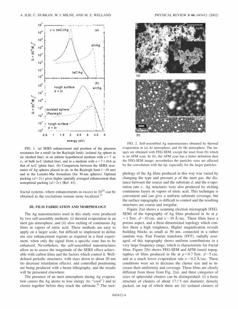
fractal systems, where enhancements in excess to 1010 can beobtained as the excitations remain more localized.31
III. FILM FABRICATION AND MORPHOLOGY
The Ag nanostructures used in this study were producedby two self-assembly methods: !i" thermal evaporation in aninert gas atmosphere, and !ii" slow etching of continuous Agfilms in vapors of nitric acid. These methods are easy toapply on a larger scale, but difficult to implement to definenm size enhancement regions as required in a final experi-ment, when only the signal from a specific zone has to beenhanced. Nevertheless, the self-assembled nanostructuresallow us to assess the magnitude of the SERS effect achiev-able with carbon films and the factors which control it. Well-defined periodic structures, with sizes down to about 20 nm!to decrease retardation effects", and controlled positioningare being produced with e-beam lithography, and the resultswill be presented elsewhere.The presence of an inert atmosphere during Ag evapora-
tion causes the Ag atoms to lose energy !to ‘‘cool’’" and tocluster together before they reach the substrate.42 The mor-
phology of the Ag films produced in this way was varied bychanging the type and pressure p of the inert gas, the dis-tance between the source and the substrate d, and the evapo-ration rate v . Ag structures were also produced by etchingcontinuous layers in vapors of nitric acid. This technique isconvenient and can give a uniform substrate coverage, butthe surface topography is difficult to control and the resultingstructures are coarse and irregular.Figure 2!a" shows a scanning electron micrograph !FEG-
SEM" of the topography of Ag films produced in Ar at p$1 Torr, d&10 cm, and v&10 Å/sec. These films have aporous aspect, and a three-dimensional topology which con-fers them a high roughness. Higher magnification revealsbuilding blocks as small as 50 nm, connected in a ratherrandom way. Fast Fourier transform !FFT", radially aver-aged, of this topography shows uniform contributions in avery large frequency range, which is characteristic for fractalfilms. Figure 2!b" shows FEG-SEM and AFM !inset" topog-raphies of films produced in He at p$0.7 Torr, d&5 cm,and at a much lower evaporation rate v&0.2 Å/sec. Theseconditions were set to decrease the cluster size and to in-crease their uniformity and coverage. These films are clearlydifferent from those from Fig. 2!a", and three categories ofsizes of spheroidal clusters can be distinguished: !i" a basicstructure of clusters of about 17&5-nm diameter, denselypacked, on top of which there are !ii" isolated clusters of
FIG. 1. !a" SERS enhancement and position of the plasmonresonance for a small !in the Rayleigh limit", isolated Ag sphere inair !dashed line", in an infinite hypothetical medium with ($7 as(1 of bulk ta-C !dotted line", and in a medium with ($7#i0.6 asthat of ta-C !plain line". !b" Comparison between the SERS reso-nance of Ag spheres placed in air, in the Rayleigh limit !&18 nm"and in the Lorentz-Mie formalism !for 30-nm spheres". Optimalpacking (d$2r) gives higher spatially averaged enhancement thannonoptimal packing (d"2r) !Ref. 41".
FIG. 2. Self-assembled Ag nanostructures obtained by thermalevaporation in !a" Ar atmosphere, and !b" He atmosphere. The im-ages are obtained with FEG-SEM, except the inset from !b" whichis an AFM scan. In !b", the AFM scan has a better definition thenthe FEG-SEM image; nevertheless the particles sizes are affectedby the convolution with the tip, especially for the larger particles.
A. ILIE, C. DURKAN, W. I. MILNE, AND M. E. WELLAND PHYSICAL REVIEW B 66, 045412 !2002"
045412-4
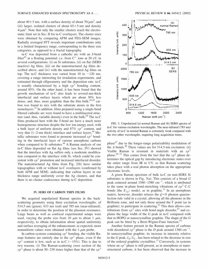
about 40&5 nm, with a surface density of about 70/#m2, and!iii" larger, isolated clusters of about 65&5 nm and density4/#m2. Note that only the smaller clusters reach the electro-static limit set in Sec. II for ta-C overlayers. The cluster sizeswere obtained by comparing AFM and FEG-SEM images.Radially averaged FFT reveals important contributions onlyin a limited frequency range, corresponding to the three sizecategories, as opposed to a fractal topography.ta-C was deposited from a cathodic arc with an S-bend
filter43 at a floating potential, i.e. from C# ions at 20 eV, inseveral configurations: !i" on Si substrates, !ii" on flat !SERSinactive" Ag films, !iii" on the nanostructured Ag films de-scribed above, and !iv" with the nanostructured Ag films ontop. The ta-C thickness was varied from 10 to &120 nm,covering a range interesting for irradiation experiments, andestimated through ellipsometry and the deposition rate. ta-Cis usually characterized by a high sp3 bonding content,around 85%. On the other hand, it has been found that thegrowth mechanism of ta-C also leads to several-nm-thickinterfacial and surface layers which are about 30% lessdense, and, thus, more graphitic than the film bulk;44,45 car-bon was found to mix with the substrate atoms in the firstmonolayers.12 In addition, films prepared using a single-bendfiltered cathodic arc were found to have a multilayered struc-ture !and, thus, variable density" even in the bulk;44 The ta-Cfilms produced here with the S-bend arc have a much morehomogeneous structure despite the low ion energy used, witha bulk layer of uniform density and 87% sp3 content, andvery thin !1–2-nm thick" interface and surface layers.44 Me-tallic substrates were found to promote increased sp2 bond-ing in the interfacial layer of various amorphous carbonswhen compared to Si substrates.46 A Raman analysis of ourta-C films deposited on flat Ag films !see Sec. IV" showedthat the interface with Ag suffers only a moderate modifica-tion compared to the interface with Si, which could be con-sistent with sp2 promotion and increased interfacial disorder.The nanostructured Ag films from Fig. 2!b" have similartopographies with or without ta-C overlayers !confirmed byboth AFM and SEM", indicating that carbon layers in ourthickness range uniformly cover the Ag clusters, and thatthere is no cluster coalescence during ta-C deposition.
IV. SERS OF CARBON THIN FILMS
We acquired unpolarized Raman spectra in the back-scattering geometry using three excitation wavelengths, of514.5 nm !green", 633 nm !red" and 785 nm !near-infrared",in order to determine the position of the plasmon resonance.Large beam as well as confocal experimental setups wereused, varying the probe size from 10 #m to about 1 #m,respectively, to obtain information about spatial uniformityand surface averaging of the enhancement; as expected, morenonuniform values were obtained with the 1-#m probe.In carbon systems containing sp2 bonding, the visible Ra-
man features are entirely due to the sp2 phase, even if thesp2 content is low, such as in ta-C !&15%". This is due totwo reasons. !i" The Raman-scattering cross section of thesp2 phase is about 50–230 times higher than that of the sp3
phase47 due to the longer-range polarizability modulation ofthe , bonds.48 These values are for 514.5-nm excitation. !ii"Visible Raman is resonant in materials with an sp2phase.49–51 This comes from the fact that the sp2 phase de-termines the optical gap by introducing electronic states overthe entire range from IR to UV, so that Raman scatteringtakes place with a real photon absorption on the appropriateelectronic levels.A green Raman spectrum of bulk ta-C on non-SERS Si
substrates is shown in Fig. 3!a". This consists of a broad Gpeak centered around 1560–1580 cm!1, which is attributedto the same in-plane bond-stretching vibrations of sp2 C-Cbonds !the E2g2 mode", as in graphite.13 In an amorphousmatrix, however, disorder relaxes the q! %0 phonon quasise-lection rule valid in a crystal, allowing all the phonons in theBrillouin zone, and not only those around the / point !as ingraphite", to participate in scattering.52 This then allows con-tributions from sp2 sites with bond angle disorder,53 and ex-plains the large width of the G peak in ta-C compared withthat in HOPG or nanocrystalline graphite. The shape of the Gpeak can be fitted by a Breit-Wigner-Fano function.54Another feature present in the Raman spectra of carbons
with disordered sp2 phase is the D peak around 1360 cm!1.In nanocrystalline graphite, its increase in intensity relativeto the G peak, ID /IG , has been related to the decrease in sizeof the ordered graphitic crystallites.13 Conversely, in systemswhere an sp3 phase is still present, as in amorphous or nano-structured carbons, it has been observed that the increase in
FIG. 3. Unpolarized !a" normal Raman and !b" SERS spectra ofta-C for various excitation wavelengths. The near-infrared !785 nm"activity of ta-C in normal Raman is extremely weak compared withthe two other wavelengths, requiring long acquisition times.
SURFACE ENHANCED RAMAN SPECTROSCOPY AS A . . . PHYSICAL REVIEW B 66, 045412 !2002"
045412-5
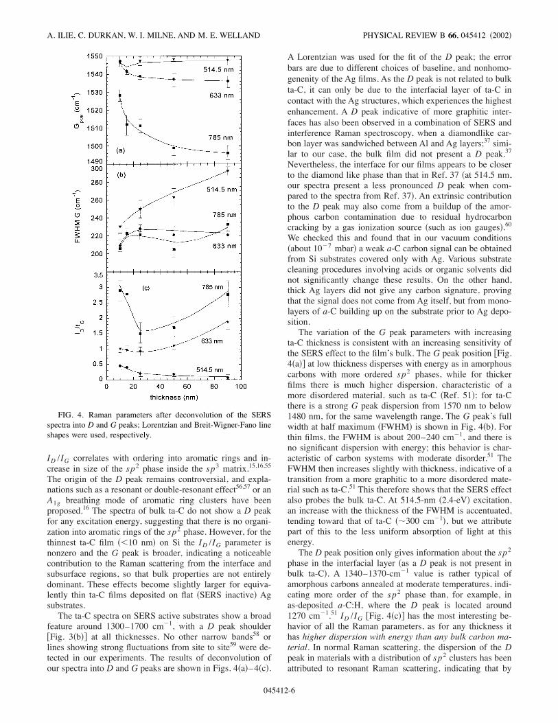
ID /IG correlates with ordering into aromatic rings and in-crease in size of the sp2 phase inside the sp3 matrix.15,16,55The origin of the D peak remains controversial, and expla-nations such as a resonant or double-resonant effect56,57 or anA1g breathing mode of aromatic ring clusters have beenproposed.16 The spectra of bulk ta-C do not show a D peakfor any excitation energy, suggesting that there is no organi-zation into aromatic rings of the sp2 phase. However, for thethinnest ta-C film !%10 nm" on Si the ID /IG parameter isnonzero and the G peak is broader, indicating a noticeablecontribution to the Raman scattering from the interface andsubsurface regions, so that bulk properties are not entirelydominant. These effects become slightly larger for equiva-lently thin ta-C films deposited on flat !SERS inactive" Agsubstrates.The ta-C spectra on SERS active substrates show a broad
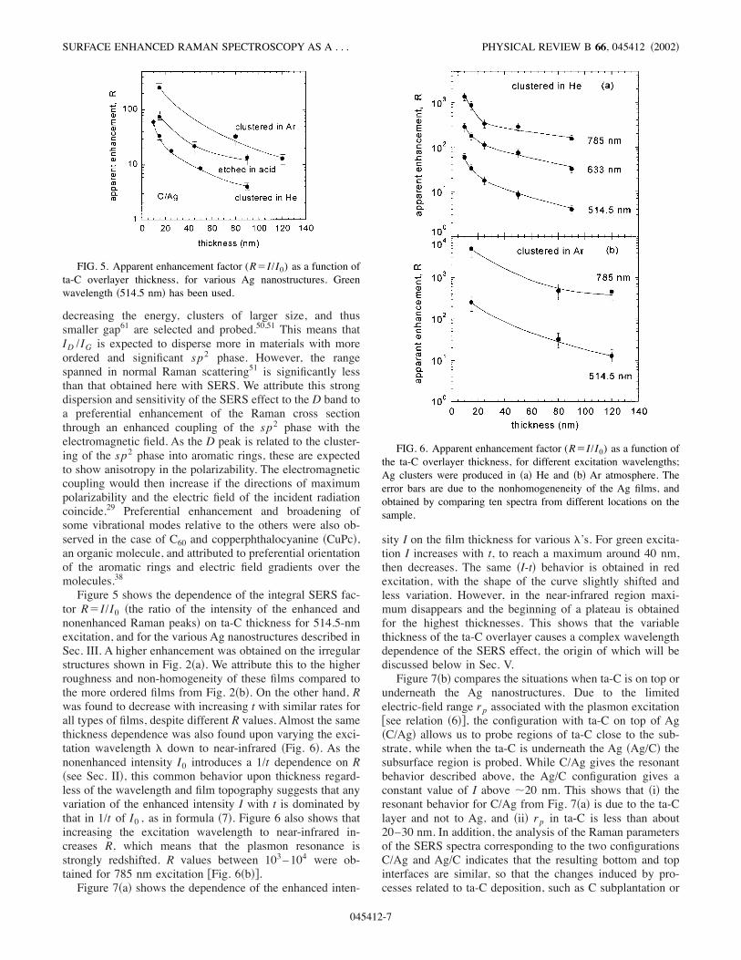
feature around 1300–1700 cm!1, with a D peak shoulder)Fig. 3!b"* at all thicknesses. No other narrow bands58 orlines showing strong fluctuations from site to site59 were de-tected in our experiments. The results of deconvolution ofour spectra into D and G peaks are shown in Figs. 4!a"–4!c".
A Lorentzian was used for the fit of the D peak; the errorbars are due to different choices of baseline, and nonhomo-genenity of the Ag films. As the D peak is not related to bulkta-C, it can only be due to the interfacial layer of ta-C incontact with the Ag structures, which experiences the highestenhancement. A D peak indicative of more graphitic inter-faces has also been observed in a combination of SERS andinterference Raman spectroscopy, when a diamondlike car-bon layer was sandwiched between Al and Ag layers;37 simi-lar to our case, the bulk film did not present a D peak.37Nevertheless, the interface for our films appears to be closerto the diamond like phase than that in Ref. 37 !at 514.5 nm,our spectra present a less pronounced D peak when com-pared to the spectra from Ref. 37". An extrinsic contributionto the D peak may also come from a buildup of the amor-phous carbon contamination due to residual hydrocarboncracking by a gas ionization source !such as ion gauges".60We checked this and found that in our vacuum conditions!about 10!7 mbar" a weak a-C carbon signal can be obtainedfrom Si substrates covered only with Ag. Various substratecleaning procedures involving acids or organic solvents didnot significantly change these results. On the other hand,thick Ag layers did not give any carbon signature, provingthat the signal does not come from Ag itself, but from mono-layers of a-C building up on the substrate prior to Ag depo-sition.The variation of the G peak parameters with increasing
ta-C thickness is consistent with an increasing sensitivity ofthe SERS effect to the film’s bulk. The G peak position )Fig.4!a"* at low thickness disperses with energy as in amorphouscarbons with more ordered sp2 phases, while for thickerfilms there is much higher dispersion, characteristic of amore disordered material, such as ta-C !Ref. 51"; for ta-Cthere is a strong G peak dispersion from 1570 nm to below1480 nm, for the same wavelength range. The G peak’s fullwidth at half maximum !FWHM" is shown in Fig. 4!b". Forthin films, the FWHM is about 200–240 cm!1, and there isno significant dispersion with energy; this behavior is char-acteristic of carbon systems with moderate disorder.51 TheFWHM then increases slightly with thickness, indicative of atransition from a more graphitic to a more disordered mate-rial such as ta-C.51 This therefore shows that the SERS effectalso probes the bulk ta-C. At 514.5-nm !2.4-eV" excitation,an increase with the thickness of the FWHM is accentuated,tending toward that of ta-C !&300 cm!1", but we attributepart of this to the less uniform absorption of light at thisenergy.The D peak position only gives information about the sp2
phase in the interfacial layer !as a D peak is not present inbulk ta-C". A 1340–1370-cm!1 value is rather typical ofamorphous carbons annealed at moderate temperatures, indi-cating more order of the sp2 phase than, for example, inas-deposited a-C:H, where the D peak is located around1270 cm!1.51 ID /IG )Fig. 4!c"* has the most interesting be-havior of all the Raman parameters, as for any thickness ithas higher dispersion with energy than any bulk carbon ma-terial. In normal Raman scattering, the dispersion of the Dpeak in materials with a distribution of sp2 clusters has beenattributed to resonant Raman scattering, indicating that by
FIG. 4. Raman parameters after deconvolution of the SERSspectra into D and G peaks; Lorentzian and Breit-Wigner-Fano lineshapes were used, respectively.
A. ILIE, C. DURKAN, W. I. MILNE, AND M. E. WELLAND PHYSICAL REVIEW B 66, 045412 !2002"
045412-6
decreasing the energy, clusters of larger size, and thussmaller gap61 are selected and probed.50,51 This means thatID /IG is expected to disperse more in materials with moreordered and significant sp2 phase. However, the rangespanned in normal Raman scattering51 is significantly lessthan that obtained here with SERS. We attribute this strongdispersion and sensitivity of the SERS effect to the D band toa preferential enhancement of the Raman cross sectionthrough an enhanced coupling of the sp2 phase with theelectromagnetic field. As the D peak is related to the cluster-ing of the sp2 phase into aromatic rings, these are expectedto show anisotropy in the polarizability. The electromagneticcoupling would then increase if the directions of maximumpolarizability and the electric field of the incident radiationcoincide.29 Preferential enhancement and broadening ofsome vibrational modes relative to the others were also ob-served in the case of C60 and copperphthalocyanine !CuPc",an organic molecule, and attributed to preferential orientationof the aromatic rings and electric field gradients over themolecules.38Figure 5 shows the dependence of the integral SERS fac-
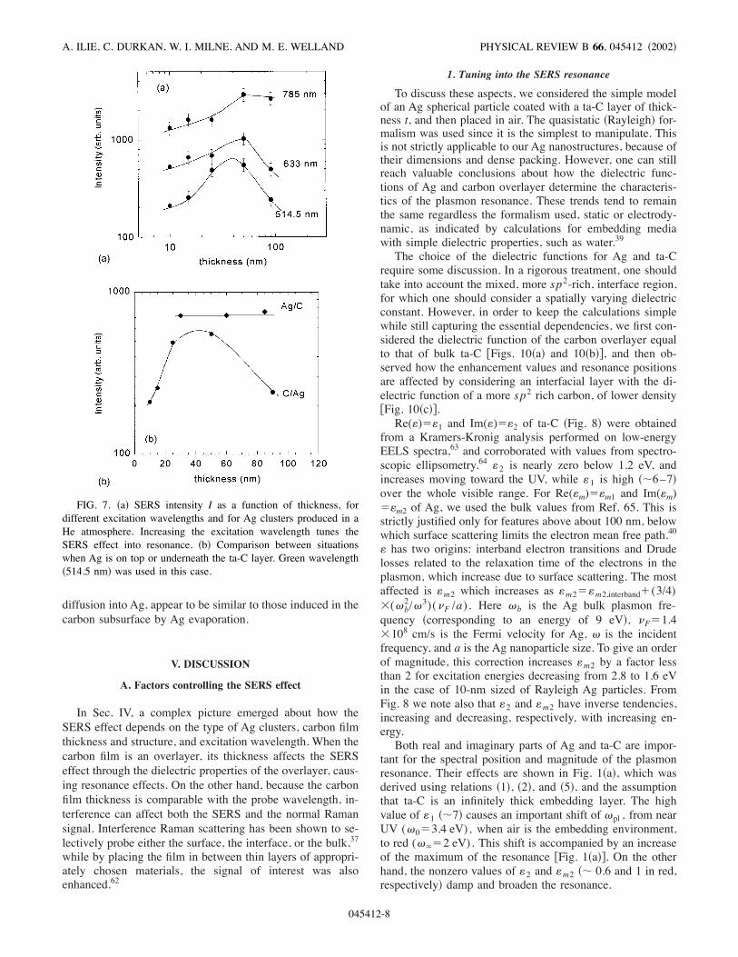
tor R$I/I0 !the ratio of the intensity of the enhanced andnonenhanced Raman peaks" on ta-C thickness for 514.5-nmexcitation, and for the various Ag nanostructures described inSec. III. A higher enhancement was obtained on the irregularstructures shown in Fig. 2!a". We attribute this to the higherroughness and non-homogeneity of these films compared tothe more ordered films from Fig. 2!b". On the other hand, Rwas found to decrease with increasing t with similar rates forall types of films, despite different R values. Almost the samethickness dependence was also found upon varying the exci-tation wavelength . down to near-infrared !Fig. 6". As thenonenhanced intensity I0 introduces a 1/t dependence on R!see Sec. II", this common behavior upon thickness regard-less of the wavelength and film topography suggests that anyvariation of the enhanced intensity I with t is dominated bythat in 1/t of I0 , as in formula !7". Figure 6 also shows thatincreasing the excitation wavelength to near-infrared in-creases R, which means that the plasmon resonance isstrongly redshifted. R values between 103– 104 were ob-tained for 785 nm excitation )Fig. 6!b"*.Figure 7!a" shows the dependence of the enhanced inten-
sity I on the film thickness for various .’s. For green excita-tion I increases with t, to reach a maximum around 40 nm,then decreases. The same !I-t" behavior is obtained in redexcitation, with the shape of the curve slightly shifted andless variation. However, in the near-infrared region maxi-mum disappears and the beginning of a plateau is obtainedfor the highest thicknesses. This shows that the variablethickness of the ta-C overlayer causes a complex wavelengthdependence of the SERS effect, the origin of which will bediscussed below in Sec. V.Figure 7!b" compares the situations when ta-C is on top or
underneath the Ag nanostructures. Due to the limitedelectric-field range rp associated with the plasmon excitation)see relation !6"*, the configuration with ta-C on top of Ag!C/Ag" allows us to probe regions of ta-C close to the sub-strate, while when the ta-C is underneath the Ag !Ag/C" thesubsurface region is probed. While C/Ag gives the resonantbehavior described above, the Ag/C configuration gives aconstant value of I above &20 nm. This shows that !i" theresonant behavior for C/Ag from Fig. 7!a" is due to the ta-Clayer and not to Ag, and !ii" rp in ta-C is less than about20–30 nm. In addition, the analysis of the Raman parametersof the SERS spectra corresponding to the two configurationsC/Ag and Ag/C indicates that the resulting bottom and topinterfaces are similar, so that the changes induced by pro-cesses related to ta-C deposition, such as C subplantation or
FIG. 5. Apparent enhancement factor (R$I/I0) as a function ofta-C overlayer thickness, for various Ag nanostructures. Greenwavelength !514.5 nm" has been used.
FIG. 6. Apparent enhancement factor (R$I/I0) as a function ofthe ta-C overlayer thickness, for different excitation wavelengths;Ag clusters were produced in !a" He and !b" Ar atmosphere. Theerror bars are due to the nonhomogeneneity of the Ag films, andobtained by comparing ten spectra from different locations on thesample.
SURFACE ENHANCED RAMAN SPECTROSCOPY AS A . . . PHYSICAL REVIEW B 66, 045412 !2002"
045412-7
diffusion into Ag, appear to be similar to those induced in thecarbon subsurface by Ag evaporation.
V. DISCUSSION
A. Factors controlling the SERS effect
In Sec. IV, a complex picture emerged about how theSERS effect depends on the type of Ag clusters, carbon filmthickness and structure, and excitation wavelength. When thecarbon film is an overlayer, its thickness affects the SERSeffect through the dielectric properties of the overlayer, caus-ing resonance effects. On the other hand, because the carbonfilm thickness is comparable with the probe wavelength, in-terference can affect both the SERS and the normal Ramansignal. Interference Raman scattering has been shown to se-lectively probe either the surface, the interface, or the bulk,37while by placing the film in between thin layers of appropri-ately chosen materials, the signal of interest was alsoenhanced.62
1. Tuning into the SERS resonance
To discuss these aspects, we considered the simple modelof an Ag spherical particle coated with a ta-C layer of thick-ness t, and then placed in air. The quasistatic !Rayleigh" for-malism was used since it is the simplest to manipulate. Thisis not strictly applicable to our Ag nanostructures, because oftheir dimensions and dense packing. However, one can stillreach valuable conclusions about how the dielectric func-tions of Ag and carbon overlayer determine the characteris-tics of the plasmon resonance. These trends tend to remainthe same regardless the formalism used, static or electrody-namic, as indicated by calculations for embedding mediawith simple dielectric properties, such as water.39The choice of the dielectric functions for Ag and ta-C
require some discussion. In a rigorous treatment, one shouldtake into account the mixed, more sp2-rich, interface region,for which one should consider a spatially varying dielectricconstant. However, in order to keep the calculations simplewhile still capturing the essential dependencies, we first con-sidered the dielectric function of the carbon overlayer equalto that of bulk ta-C )Figs. 10!a" and 10!b"*, and then ob-served how the enhancement values and resonance positionsare affected by considering an interfacial layer with the di-electric function of a more sp2 rich carbon, of lower density)Fig. 10!c"*.Re(()$(1 and Im(()$(2 of ta-C !Fig. 8" were obtained
from a Kramers-Kronig analysis performed on low-energyEELS spectra,63 and corroborated with values from spectro-scopic ellipsometry.64 (2 is nearly zero below 1.2 eV, andincreases moving toward the UV, while (1 is high !&6–7"over the whole visible range. For Re((m)$(m1 and Im((m)$(m2 of Ag, we used the bulk values from Ref. 65. This isstrictly justified only for features above about 100 nm, belowwhich surface scattering limits the electron mean free path.40( has two origins: interband electron transitions and Drudelosses related to the relaxation time of the electrons in theplasmon, which increase due to surface scattering. The mostaffected is (m2 which increases as (m2$(m2,interband#(3/4)'('b
2/'3)(0F /a). Here 'b is the Ag bulk plasmon fre-quency !corresponding to an energy of 9 eV", 0F$1.4'108 cm/s is the Fermi velocity for Ag, ' is the incidentfrequency, and a is the Ag nanoparticle size. To give an orderof magnitude, this correction increases (m2 by a factor lessthan 2 for excitation energies decreasing from 2.8 to 1.6 eVin the case of 10-nm sized of Rayleigh Ag particles. FromFig. 8 we note also that (2 and (m2 have inverse tendencies,increasing and decreasing, respectively, with increasing en-ergy.Both real and imaginary parts of Ag and ta-C are impor-
tant for the spectral position and magnitude of the plasmonresonance. Their effects are shown in Fig. 1!a", which wasderived using relations !1", !2", and !5", and the assumptionthat ta-C is an infinitely thick embedding layer. The highvalue of (1 !&7" causes an important shift of 'pl , from nearUV ('0$3.4 eV), when air is the embedding environment,to red ('1$2 eV). This shift is accompanied by an increaseof the maximum of the resonance )Fig. 1!a"*. On the otherhand, the nonzero values of (2 and (m2 !& 0.6 and 1 in red,respectively" damp and broaden the resonance.
FIG. 7. !a" SERS intensity I as a function of thickness, fordifferent excitation wavelengths and for Ag clusters produced in aHe atmosphere. Increasing the excitation wavelength tunes theSERS effect into resonance. !b" Comparison between situationswhen Ag is on top or underneath the ta-C layer. Green wavelength!514.5 nm" was used in this case.
A. ILIE, C. DURKAN, W. I. MILNE, AND M. E. WELLAND PHYSICAL REVIEW B 66, 045412 !2002"
045412-8
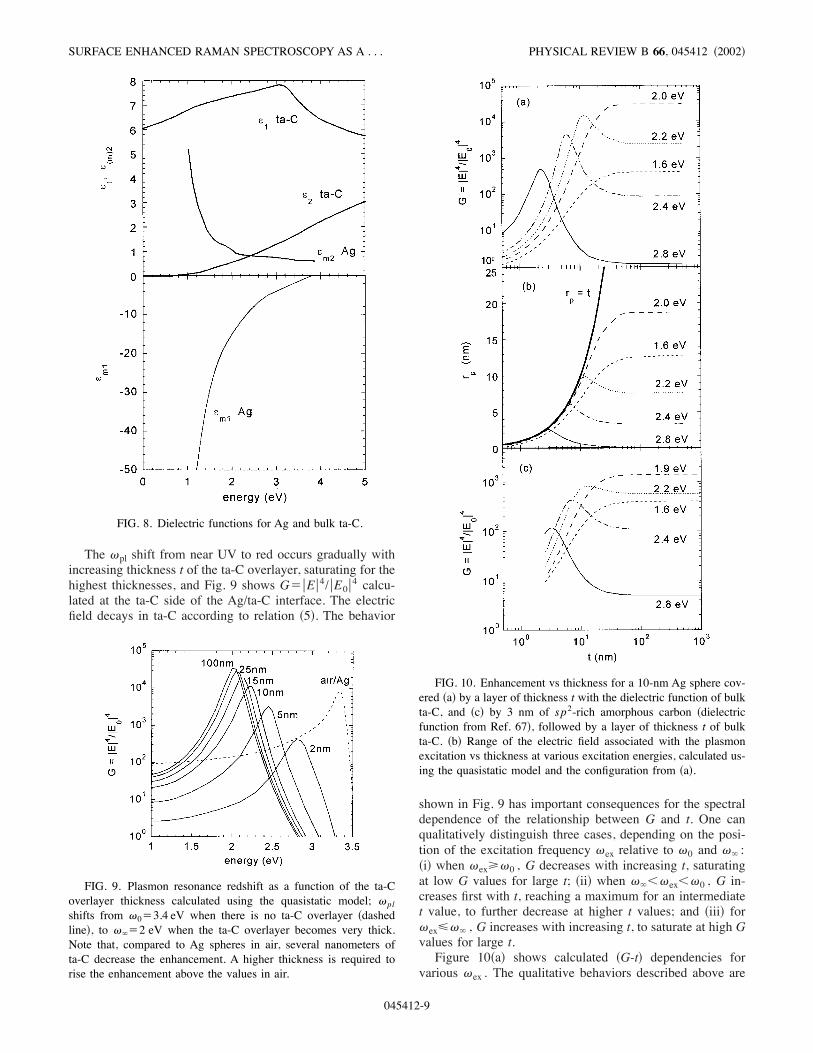
The 'pl shift from near UV to red occurs gradually withincreasing thickness t of the ta-C overlayer, saturating for thehighest thicknesses, and Fig. 9 shows G$!E!4/!E0!4 calcu-lated at the ta-C side of the Ag/ta-C interface. The electricfield decays in ta-C according to relation !5". The behavior
shown in Fig. 9 has important consequences for the spectraldependence of the relationship between G and t. One canqualitatively distinguish three cases, depending on the posi-tion of the excitation frequency 'ex relative to '0 and '1 :!i" when 'ex2'0 , G decreases with increasing t, saturatingat low G values for large t; !ii" when '1%'ex%'0 , G in-creases first with t, reaching a maximum for an intermediatet value, to further decrease at higher t values; and !iii" for'ex3'1 , G increases with increasing t, to saturate at high Gvalues for large t.Figure 10!a" shows calculated !G-t" dependencies for
various 'ex . The qualitative behaviors described above are
FIG. 8. Dielectric functions for Ag and bulk ta-C.
FIG. 9. Plasmon resonance redshift as a function of the ta-Coverlayer thickness calculated using the quasistatic model; 'plshifts from '0$3.4 eV when there is no ta-C overlayer !dashedline", to '1$2 eV when the ta-C overlayer becomes very thick.Note that, compared to Ag spheres in air, several nanometers ofta-C decrease the enhancement. A higher thickness is required torise the enhancement above the values in air.
FIG. 10. Enhancement vs thickness for a 10-nm Ag sphere cov-ered !a" by a layer of thickness t with the dielectric function of bulkta-C, and !c" by 3 nm of sp2-rich amorphous carbon !dielectricfunction from Ref. 67", followed by a layer of thickness t of bulkta-C. !b" Range of the electric field associated with the plasmonexcitation vs thickness at various excitation energies, calculated us-ing the quasistatic model and the configuration from !a".
SURFACE ENHANCED RAMAN SPECTROSCOPY AS A . . . PHYSICAL REVIEW B 66, 045412 !2002"
045412-9
retrieved. Moreover, one can see that there is a ‘‘spectralwindow’’ for 'ex , outside which the maximum enhancementbegins to fall rapidly; here this is about 1.6–2.4 eV. This isdue to (2 and (m2 increasing significantly at each side of thespectral window !see Fig. 8". The surface scattering correc-tion to (m2 described above affects the enhancement at reso-nance shown in Fig. 10!a" by less than 10%. The electric-field range rp , as defined in Sec. II, was also calculated, andfound to follow almost the same dependence on t as G at theAg/ta-C interface )Fig. 10!b"*. Therefore, the SERS intensityI obtained by integration according to Relation !6" will dothe same, and this accounts for the shape of the experimental(I-t) dependencies from Fig. 7!a" for situations when '1%'ex%'0 and 'ex3'1 . Note that Figs. 7!a" and 10!a"should be compared only qualitatively. In Fig. 7!a" the over-all variation across the thickness range is much less pro-nounced than in the simulations, while the maximum posi-tion also shifts less. This can be explained by broadening andred-shifting of the theoretical resonances from Fig. 10!a" dueto larger-size particles and electromagnetic coupling in theactual Ag nanostructures, as discussed in Sec. II.Figure 10!b" shows, as a function of t and 'ex , what
fraction of t, rp /t , is probed by SERS. The line rp$t indi-cates the limit case when the SERS signal would originatefrom the entire thickness t, while departing from it indicatesthat a decreasingly small fraction contributes. Also note thateven for regions in the plasmon electric field range rp , thecontribution to SERS is uneven as the electric field decaysrapidly as (a/r)12.66 This also means that by increasing theparticle size a, one can increase the range of the plasmoneffect. Figure 10!b" exemplifies how appropriate choices of tand 'ex can be used to selectively probe different film re-gions. For t2100 nm, only a fraction of t is probed even inthe most favorable case !about 20% at 'ex$1.8 eV". Increas-ing t and decreasing 'ex strongly reduces rp /t . On the otherhand, for small t (10%t%30 nm), a much higher percentage,about 40–100%, is probed at all 'ex values; while for verysmall t !%10 nm" the whole layer can be probed at high 'ex .Moreover, for each t there is a resonant 'ex at which rp /t ismaximum. The reduced SERS range compared with the filmthickness for larger t values confines the active layer near theta-C substrate interface, so that there is only little thicknessdependence of the enhanced intensity I through rp , in con-trast with the nonenhanced intensity I0 which is obtained inequal measure from the whole ta-C layer. This confirms thatthe experimental decay of I/I0 with t from Figs. 5 and 6occurs from I0 , as explained in Sec. IV.The thickness independence of I with t for thicker films
with Ag nanostructures on top )Fig. 7!b"* can now be under-stood. Now the embedding medium is air, so that there is noreason for 'pl to redshift with decreasing the ta-C under-layer thickness. Therefore, for a rough surface like in Fig.1!b", 'pl should be in the 2.8–3-eV range. Moreover, theconstancy of I with decreasing t down to about 20–30 nm isin agreement with the range rp calculated above.The values reported above in Fig. 10!a", obtained by us-
ing the optical constants of bulk ta-C are modified by thepresence at the interface with Ag of a few nanometers of amore sp2 rich material !as mentioned in Secs. III and IV".
Figure 10!c" shows the results of the quasistatic simulationfor the four-layer system describing this situation: an Agsphere !10-nm diameter"/3 nm of sp2-rich amorphous car-bon, of density 2.2 g/cm3/bulk ta-C/air. The 3-nm sp2-richinterfacial layer makes the maximum enhancement G de-crease moderately when compared to Fig. 10!a", by aboutone order of magnitude at a given wavelength, and slightlyshifts the resonance position from 2 to 1.9 eV.
2. Interference
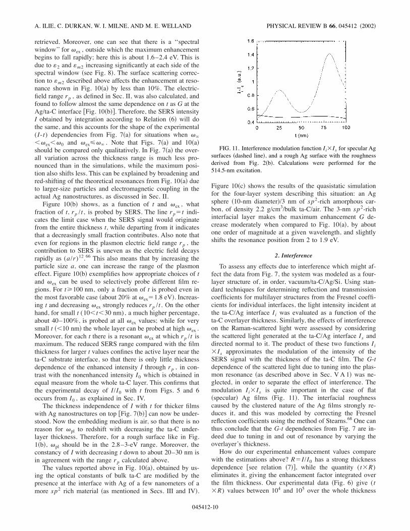
To assess any effects due to interference which might af-fect the data from Fig. 7, the system was modeled as a four-layer structure of, in order, vacuum/ta-C/Ag/Si. Using stan-dard techniques for determining reflection and transmissioncoefficients for multilayer structures from the Fresnel coeffi-cients for individual interfaces, the light intensity incident atthe ta-C/Ag interface I i was evaluated as a function of theta-C overlayer thickness. Similarly, the effects of interferenceon the Raman-scattered light were assessed by consideringthe scattered light generated at the ta-C/Ag interface Is anddirected normal to it. The product of these two functions I i'Is approximates the modulation of the intensity of theSERS signal with the thickness of the ta-C film. The G-tdependence of the scattered light due to tuning into the plas-mon resonance !as described above in Sec. VA 1" was ne-glected, in order to separate the effect of interference. Themodulation I i'Is is quite important in the case of flat!specular" Ag films !Fig. 11". The interfacial roughnesscaused by the clustered nature of the Ag films strongly re-duces it, and this was modeled by correcting the Fresnelreflection coefficients using the method of Stearns.68 One canthus conclude that the G-t dependencies from Fig. 7 are in-deed due to tuning in and out of resonance by varying theoverlayer’s thickness.How do our experimental enhancement values compare
with the estimations above? R$I/I0 has a strong thicknessdependence )see relation !7"*, while the quantity (t'R)eliminates it, giving the enhancement factor integrated overthe film thickness. Our experimental data !Fig. 6" give (t'R) values between 104 and 105 over the whole thickness
FIG. 11. Interference modulation function I i'Is for specular Agsurfaces !dashed line", and a rough Ag surface with the roughnessderived from Fig. 2!b". Calculations were performed for the514.5-nm excitation.
A. ILIE, C. DURKAN, W. I. MILNE, AND M. E. WELLAND PHYSICAL REVIEW B 66, 045412 !2002"
045412-10
range at 785-nm excitation. These values are above thoseobtained in Fig. 10!c", when the sp2-rich interfacial layerwas taken into account. This indicates that resonance cou-pling between closely packed particles, like the 20-nm struc-tures from Fig. 2!b", might take place. Indeed, from electro-dynamic simulations for of rough surface formed by packedsemispherical particles of 30 nm,41 an optimal packing of theparticles )i.e., d$2r in Fig. 1!b"* would give averaged en-hancement factors up to 106, while if the packing is slightlynonoptimal (d"2r), the enhancement falls to below 104.For the random films from Fig. 2!a" it is possible that ‘‘hotspots’’ are responsible for the enhancement. Nevertheless,from our measurements with a micron size beam there is nodirect evidence to support this fact, as in Ref. 59, as the siteto site fluctuations recorded here reached only a factor ofabout 5.
B. Enhancement contrast and material identification
Figure 1!a" shows that Im(()$(2 of the overlayer causesdamping of the resonance. Consequently, SERS works betteron carbon materials with low (2 in the visible range such asta-C. C60 and fullerite are other good cases, as (2 is nearlyzero for energies below 2 eV.69 At the other extreme, there isgraphite, whose (2 values in visible reach 8–9. This makesgraphite inactive for SERS. Other materials, like amorphouscarbons deposited in various conditions have (2 values lyingin between these two extremes.70,71 One can pass from amor-phous carbon to nanocrystalline graphite in a continuoustransition, either using thermal annealing, or high-energyparticle irradiation. In such a transition, the amorphous net-work undergoes several transformations: !i" there is sp3 tosp2 conversion, and !ii" clustering of the sp2 phase intomore stable aromatic rings.15,16 By increasing the annealingtemperature or the irradiation dose, sp2 clusters of increasingsize form in the amorphous sp3 matrix, until this disappearsand the material transforms into nanocrystalline graphite.The graphitization induced by irradiation can affect theSERS effect in three ways.
!i" The clustering of the sp2 phase into aromatic ringsaffects the shape of the Raman spectrum, through the D peakaround 1360 cm!1.15,16,55 With an increasing size of aromaticclusters, the D peak increases relative to the G peak, so thatthe Raman parameter I(D)/I(G) increases. The Raman in-tensity also increases with sp3 to sp2 conversion as the sp2phase has a higher cross section than the sp3 phase !see Sec.IV".
!ii" In the transition toward nanocrystalline graphite, ananisotropy of the polarizability occurs as the sp2 aromaticclusters tend to orient in preferential planes, so that the maxi-mum polarizability is in the plane of the aromatic clusters.During post-deposition thermal annealing the sp2 aromaticclusters tend to orient in planes parallel to the substrate,72while high-energy particle irradiation aligns them perpen-dicular to the substrate.73 Therefore the coupling with theelectromagnetic field in SERS can be maximized if the di-rection of the incident electric field is in the plane of the sp2aromatic clusters. The effect of the polarizability orientation,
when perpendicular or parallel to the electric field, has beendemonstrated in experiments using polyimide molecules.74
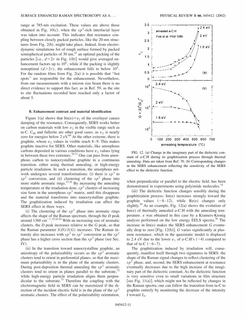
!iii" The dielectric function changes sensibly during thegraphitization process: Im(() increases strongly toward thegraphite values !&8–12", while Re(() changes onlyslightly.70 As an example, Fig. 12!a" shows the evolution ofIm(() of thermally annealed a-C:H with the annealing tem-perature. ( was obtained in this case by a Kramers-Kroniganalysis performed on the low energy EELS spectra.70 Theincrease in Im(() makes the SERS enhancement G eventu-ally drop to zero )Fig. 12!b"*. G varies significantly at plas-mon resonance, which in the quasistatic model is displacedto 2.4 eV due to the lower (1 of a-C:H’s !&4" compared tothat of ta-C !&6–7".The graphitization induced by irradiation will, conse-
quently, manifest itself through two signatures in SERS: theshape of the Raman signal changes to reflect clustering of thesp2 phase, and, second, the SERS enhancement at resonanceeventually decreases due to the high increase of the imagi-nary part of the dielectric constant. As the dielectric functionis very sensitive even to small variations in film structure)see Fig. 11!a"*, which might not be reflected by changes inthe Raman spectra, one can follow the transition from ta-C tographite entirely by monitoring the decrease of the intensityI toward I0 .
FIG. 12. !a" Change in the imaginary part of the dielectric con-stant of a-C:H during its graphitization process through thermalannealing. Data are taken from Ref. 70. !b" Corresponding changesin the SERS enhancement reflecting the sensitivity of the SERSeffect to the dielectric function.
SURFACE ENHANCED RAMAN SPECTROSCOPY AS A . . . PHYSICAL REVIEW B 66, 045412 !2002"
045412-11
VI. CONCLUSION
We investigated the possibility of achieving nanometer-scale sensitivity in a surface enhanced Raman experimentwhile using larger-sized probes of 0.1–1 #m. Carbon over-layers cover Ag nanostructures so that regions close to thefilm-substrate interface are probed, this geometry comple-menting the surface sensitive scanning near-field techniques.The main application targeted was carbon film transforma-tion under e-beam irradiation, and here we discussed, as anexample, the transformation of tetrahedral amorphous carbon!ta-C" into nanocrystalline graphite. The SERS effect withta-C as the overlayer was found to depend on the Ag nano-structure size, overlayer thickness, and excitation wave-length. Enhancement factors, averaged over the film thick-ness and a #m2 size area, of about 103– 104 were obtainedfor several tens of nm thick ta-C overlayers at resonance, inthe nearinfrared. Modulations of the enhancement with theoverlayer thickness were attributed to tuning in and out ofthe SERS resonance, while interference effects were highly
reduced due to the rough nature of the Ag films. The SERSeffect is highly sensitive to the more sp2-rich interfaciallayer of ta-C, though it also extends into the film’s bulk. Thissensitivity is increased by a selective enhancement of theRaman D band, attributed to an increased coupling caused bythe alignment of the direction of maximum polarizability tothe incident electric field. The change of the overlayer dielec-tric function upon irradiation can be used to produce an en-hancement contrast, and allows a material identification. Thiscontrast based technique could be extended to other non-carbon materials and to local mapping of dielectric proper-ties of materials.
ACKNOWLEDGMENTS
The authors wish to thank Dr. D. R. Richards for manyuseful comments, and Professor T. W. Clyne and D. Roy forhelp with the Raman facilities. A.I. gratefully acknowledgesa Research Fellowship from Girton College, Cambridge.
*Corresponding author. Email address: [email protected]. A. Talin, L. S. Pan, K. F. McCarty, T. E. Felter, H. J. Doerr,and R. F. Bunshah, Appl. Phys. Lett. 69, 3842 !1996".
2B. F. Coll, J. E. Jaskie, J. L. Markham, E. P. Menu, A. A. Talin,and P. von Allmen, in Covalently Bonded Disordered Thin-FilmMaterials, edited by M. P. Siegal, J. G. Jaskie, and W. Milens,MRS Symposia Proceedings, No. 498 !Materials Research So-ciety Pittsburgh, PA, 1998", p. 185.
3A. N. Obralsov, I. Yu. Pavlovsky, A. P. Volkov, J. Vac. Sci. Tech-nol. B 17, 674 !1999".
4G. A. J. Amaratunga, M. Baxendale, N. Rupesinghe, I. Alenxan-drou, M. Chhowala, T. Butler, A. Munindradasa, C. J. Kiely, L.Zhang, and T. Sakai, New Diamond Front. Carbon Technol. 9,31 !1999".
5B. S. Satyanarayana, J. Robertson, and W. I. Milne, J. Appl. Phys.87, 3126 !2000".
6A. Ilie, A. C. Ferrari, T. Yagi, S. E. Rodil, and J. Robertson, J.Appl. Phys. 90, 2024 !2001".
7D. R. McKenzie, W. T. Li, E. G. Gerstner, A. Merchant, D. G.McCulloch, N. A. Marks, and M. M. Bilek, Diamond Relat.Mater. 10, 230 !2001".
8D. G. McCulloch, E. G. Gerstner, D. R. McKenzie, S. Prawer,and R. Kalish, Phys. Rev. B 52, 850 !1995"; M. Waiblinger, Ch.Sommerhalter, B. Pietzak, J. Krauser, B. Mertsacker, M. Ch.Lux-Steiner, S. Klaumunzer, A. Weidinger, C. Ronning, and H.Hofsass, Appl. Phys. A: Mater. Sci. Process. 69, 239 !1999".
9D. Ugarte, Nature !London" 359, 707 !1992"; T. Cabioc’h, J. P.Riviere, and J. Delafond, J. Mater. Sci. 30, 4787 !1995".
10F. Banhart and P. M. Ajayan, Nature !London" 382, 433 !1996".11C. A. Davis, D. R. McKenzie, Y. Yin, E. Kravtchinskaia, G. A. J.Amaratunga, and V. S. Veerasamy, Philos. Mag. B 69, 1133!1994".
12C. A. Davis, G. A. J. Amaratunga, and K. M. Knowles, Phys. Rev.Lett. 80, 3280 !1998".
13F. Tuinstra and J. L. Koening, J. Chem. Phys. 53, 1126 !1970".14R. J. Nemanich and S. A. Solin, Phys. Rev. B 20, 392 !1979".15R. O. Dillon, J. A. Woollam, and V. Karkanant, Phys. Rev. B 29,
3482 !1984"; M. A. Tamor and W. C. Vassel, J. Appl. Phys. 76,3823 !1994".
16A. C. Ferrari and J. Robertson, Phys. Rev. B 61, 14 095 !2000".17A. M. Rao, F. Richter, S. Bandow, B. Chase, P. C. Eklund, K. A.Williams, S. Fang, K. R. Subbaswamy, M. Menon, A. Thess, R.E. Smalley, G. Dresselhaus, and M. S. Dresselhaus, Science 275,187 !1997".
18R. J. Nemanich, Annu. Rev. Mater. Sci. 21, 535 !1991"; S. Prawerand K. W. Nugent, in Amorphous Carbon: State of the Art, ed-ited by S. R. P. Silva, J. Robertson, W. I. Milne, and G. A. J.Amaratunga !World Scientific, Singapore, 1998".
19G. S. Duesberg, J. Muster, M. Burghard, H. J. Byrne, and S. Roth,AIP Conf. Proc. 486, 338 !1999"; K. Kneipp, H. Kneipp, P.Corio, S. D. M. Brown, K. Shafer, J. Motz, L. T. Perelman, E. B.Hanlon, A. Marucci, G. Dresselhaus, and M. S. Dresselhaus,Phys. Rev. Lett. 84, 3470 !2000".
20P. Hildebrandt and M. Stockburger, J. Phys. Chem. 88, 5935!1984"; J. T. Golab, J. R. Sprague, K. T. Carron, G. C. Schatz,and R. P. van Duyne, J. Chem. Phys. 88, 7942 !1988"; K.Kneipp, Y. Wang, H. Kneipp, I. Itzkan, R. R. Dasari, and M. S.Feld, Phys. Rev. Lett. 76, 2444 !1996".
21S. Nie and S. R. Emory, Science 275, 1102 !1997".22M. Moskovits and D. DiLella, in Surface Enhanced Raman Scat-
tering, edited by R. K. Chang and T. E. Furtak !Plenum, NewYork, 1982", p. 243.
23T. Lopez-Rios, Diamond Relat. Mater. 5, 608 !1996".24D. S. Knight, R. Weimer, L. Pilione, and W. B. White, Appl. Phys.Lett. 56, 1320 !1990".
25D. A. Smith, S. Webster, M. Ayad, S. D. Evans, D. Fogherty, andD. Batchelder, Ultramicroscopy 61, 247 !1995".
26V. Deckerr, D. Zeisel, R. Zenobi, and T. Vo-Dinh, Anal. Chem.70, 2646 !1998".
27R. Stoeckle, Y. D. Suh, V. Deckert, and R. Zenobi, Chem. Phys.Lett. 318, 131 !2000".
28P. J. Fallon, V. S. Veerasamy, C. A. Davis, J. Robertson, G. A. J.Amaratunga, W. I. Milne, and J. Koskinen, Phys. Rev. B 48,4777 !1993".
A. ILIE, C. DURKAN, W. I. MILNE, AND M. E. WELLAND PHYSICAL REVIEW B 66, 045412 !2002"
045412-12
29M. Moskovits, Rev. Mod. Phys. 57, 783 !1985".30 J. P. Kottmann, O. J. F. Martin, D. R. Smith, and S. Schultz, Phys.Rev. B 64, 235402 !2001".
31V. M. Shalaev and A. K. Sarychev, Phys. Rev. B 57, 13 265!1998".
32F. Brouers, S. Blacher, A. N. Lagarkov, A. K. Sarychev, P.Gadenne, and V. M. Shalaev, Phys. Rev. B 55, 13 234 !1997".
33V. A. Markel, V. M. Shalaev, P. Zhang, W. Huynh, L. Tay, T. L.Haslett, and M. Moskovits, Phys. Rev. B 59, 10 903 !1999".
34A. Downes, M. E. Taylor, and M. E. Welland, Phys. Rev. B 57,6706 !1998".
35K. B. K. Teo, S. E. Rodil, J. T. H. Tsai, A. C. Ferrari, J. Robert-son, and W. I. Milne, J. Appl. Phys. 89, 3706 !2001".
36M. Ramsteiner, C. Wild, and J. Wagner, Appl. Opt. 28, 4017!1989".
37L. Yu. Khriachtchev, R. Lappalainen, and M. Rasanen, DiamondRelat. Mater. 7, 1451 !1998".
38O. Stenzel, A. Stendal, D. Drews, T. Werninghaus, M. Falke, D.R. T. Zahn, and C. von Borczyskowski, Appl. Surf. Sci. 108, 71!1997".
39P. W. Barber, R. K. Chang, and H. Massoudi, Phys. Rev. B 27,7251 !1983".
40 J. A. A. J. Perenboom and P. Wyder, Phys. Rep. 78, 173 !1981".41F. J. Garcia-Vidal and J. B. Pendry, Phys. Rev. Lett. 77, 1163
!1996".42P. Milani and S. Iannotta, Cluster Beam Synthesis of Nanostruc-
tured Materials, Springer Series in Cluster Physics !Springer,Berlin, 1999".
43X. Shi, B. G. Tay, and S. P. Lau, Int. J. Mod. Phys. B 14, 136!2000".
44A. LiBassi, A. C. Ferrari, V. Stolojan, B. K. Tanner, J. Robertson,and L. M. Brown, Diamond Relat. Mater. 9, 771 !2000".
45A. Ilie, A. Hart, A. J. Flewitt, J. Robertson, and W. I. Milne, J.Appl. Phys. 88, 6002 !2000".
46P. D. Maguire, D. P. Magill, A. A. Ogwu, and J. A. McLaughlin,Diamond Relat. Mater. 10, 216 !2001"; C. Srividya and S. V.Babu, Chem. Mater. 8, 2528 !1996"; D. P. Butt, K. C. Walter, M.Nastasi, A. L. Campuzano, P. S. Martin, B. P. Wood, D. J. Rej,and G. G. Miller, Philos. Mag. Lett. 70, 385 !1994"; C. Sella, J.Lecoeur, Y. Sampeur, and P. Catania, Surf. Coat. Technol. 60,577 !1993".
47N. Wada and S. A. Solin, Physica B & C 105, 353 !1980"; S. R.Salis, D. J. Gardiner, M. Bowden, J. Savage, and D. Rodvany,Diamond Relat. Mater. 5, 589 !1996".
48C. A. Coulson and H. C. Longuet-Higgins, Proc. R. Soc. London,Ser. A 191, 447 !1947"; D. Beeman and R. Alben, Adv. Phys. 26,339 !1977".
49R. P. Vidano, D. B. Fischbach, L. J. Willis, and T. M. Loehr, SolidState Commun. 39, 341 !1981".
50M. Ramsteiner and J. Wagner, Appl. Phys. Lett. 51, 1355 !1987";I. Pocsik, M. Koos, M. Hundhausen, and L. Ley, in AmorphousCarbon: State of the Art, edited by S. R. P. Silva, J. Robertson,
W. I. Milne, and G. A. J. Amaratunga !World Scientific, Sin-gapore, 1998", p. 224.
51A. C. Ferrari and J. Robertson, Phys. Rev. B 64, 075414 !2001".52R. J. Nemanich, S. A. Solin, and R. M. Martin, Phys. Rev. B 23,6348 !1981".
53 J. S. Lannin, J. Non-Cryst. Solids 97, 39 !1987".54S. Prawer, K. W. Nugent, Y. Lifshitz, G. D. Lempert, E. Gross-man, J. Kulik, I. Avigal, and R. Kalish, Diamond Relat. Mater. 5,433 !1996".
55 J. Robertson, Prog. Solid State Chem. 21, 199 !1991".56C. Thomsen and S. Reich, Phys. Rev. B 85, 5214 !2000".57 I. Pocsik, M. Hundhausen, M. Koos, and L. Ley, J. Non-Cryst.Solids 227, 1083 !1998".
58M. B. Tzolov, N. V. Tzenov, D. I. Dimova-Malinovska, and D. Y.Yankov, Appl. Phys. Lett. 62, 2396 !1993".
59A. Kudelski and B. Pettinger, Chem. Phys. Lett. 321, 356 !2000".60 J. C. Tsang, J. E. Demuth, P. N. Sanda, and J. R. Kirtley, Chem.Phys. Lett. 76, 54 !1980".
61 J. Robertson and R. P. O’Reilly, Phys. Rev. B 35, 2946 !1987".62R. J. Nemanich, C. C. Tsai, and G. A. N. Connell, Phys. Rev. Lett.44, 273 !1980"; R. J. Nemanich, C. C. Tsai, M. J. Thompson,and T. W. Sigmon, J. Vac. Sci. Technol. 19, 685 !1981".
63S. Waidmann, M. Knupfer, J. Fink, B. Kleinsorge, and J. Robert-son, Diamond Relat. Mater. 9, 722 !2000".
64Z. Y. Chen and J. P. Zhao, J. Appl. Phys. 87, 4268 !2000".65W. D. Lynch and W. R. Hunter, in Handbook of Optical Constants
of Solids, edited by E. D. Palik, !Academic, New York, 1985".66S. L. McCall, P. M. Platzmann, and P. A. Wolff, Phys. Lett. 77A,381 !1980"; M. Kerker, D. S. Wang, and H. Chew, Appl. Opt.19, 3373 !1980".
67Handbook of Optical Constants of Solids, edited by E. D. Palik,!Academic, New York, 1985".
68D. G. Steams, J. Appl. Phys. 65, 491 !1989".69S. L. Ren, Y. Wang, A. M. Rao, E. McRae, J. M. Holden, T.Hager, K. Wang, W.-T. Lee, W. F. Ni, J. Selegue, and P. C.Eklund, Appl. Phys. Lett. 59, 2678 !1991"; G. Guizzetti, F. Ma-rabelli, M. Patrini, V. Capozzi, G. F. Lorusso, A. Minafra, M.Manfredini, and P. Milani, Phys. Status Solidi B 183, 267!1994".
70 J. Fink, Th. Mueller-Heinzerling, J. Pflueger, and B. Scheerer, B.Dischler, P. Koidl, A. Bubenzer, and R. E. Sah, Phys. Rev. B 30,4713 !1984".
71Y. Lifshitz, G. D. Lempert, E. Grossman, H. J. Scheibe, S. Voell-mar, B. Schultrich, A. Breskin, R. Chechik, E. Shefer, D. Bacon,R. Kalish, and A. Hoffman, Diamond Relat. Mater. 6, 687!1997".
72 J. P. Sullivan, T. A. Friedmann, and A. G. Baca, J. Electron.Mater. 26, 1021 !1997".
73S. S. Kim, S. Hishita, T. S. Cho, and J. H. Je, J. Appl. Phys. 88, 55!2000".
74W. H. Tsai, J. T. Young, F. J. Boerio, and P. P. Hong, Langmuir 7,745 !1991".
SURFACE ENHANCED RAMAN SPECTROSCOPY AS A . . . PHYSICAL REVIEW B 66, 045412 !2002"
045412-13
Related Documents