Surface energy patterning for inkjet printing in device fabrication Jian Lin * a , Per Dahlsten b , Jussi Pekkanen c , Mika Linden b , Matti Mäntysalo c , and Ronald Österbacka a a Department of Physics and Center for Functional Materials, Åbo Akademi University, Porthansgatan 3, FI-20500 Turku, Finland b Department of Physical Chemistry and Center for Functional Materials, Åbo Akademi University, Porthansgatan 3, FI-20500 Turku, Finland c Department of Electronics, Tampere University of Technology, P.O. box 692 FI-33101 Tampere, Finland. ABSTRACT For application of device fabrication by inkjet printing, an accurate and high resolution patterning method is required. However, high resolution inkjet printing, which limited by the inkjet nozzles and the ink movements, is one of the most challenging issues at present. An enhanced control of ink flow and spread by surface energy patterning on substrates can be used to improve the resolution and quality of the inkjet printed devices. Our strategy is depositing a hydrophobic pattern on a hydrophilic substrate, and thereafter inkjet printing the functional ink on top of the surface energy pattern. High surface energy contrast patterns on polyimide were got by microcontact printing, which can make ink moving from hydrophobic area to hydrophilic polyimide substrate. Inkjet printed silver patterns with 15 m thin gaps were obtained by the surface energy pattern. This visible and easy processing pattern can be used widely in inkjet printing for higher resolution, more precise pattern, and smaller devices. Keywords: Inkjet printing, octadecyltrichlorosilane, surface energy pattern, thin gap. 1. INTRODUCTION Inkjet printing has become a revolutionary technology aimed at low-cost and flexible device manufacture on plastic substrate. It provides a potential pathway toward the realization of printed electronics in polymer transistors, [1] display, [2] radio frequency identification (RFID), [3] and memory device. [4] More and more materials, [5] such as functional polymers and metal-containing inks, have been successfully patterned using inkjet printing on variety of substrates. However, high-resolution and fine pitch electrodes, and short channel transistors are necessary for high performance integrated circuits and display. It became one of the most challenging issues for inkjet printing technologies. * [email protected] ; phone 358 2 2154 606; fax 358 2 2154 776 Organic Field-Effect Transistors VIII, edited by Zhenan Bao, Iain McCulloch, Proc. of SPIE Vol. 7417 74171D · © 2009 SPIE · CCC code: 0277-786X/09/$18 · doi: 10.1117/12.825856 Proc. of SPIE Vol. 7417 74171D-1

Welcome message from author
This document is posted to help you gain knowledge. Please leave a comment to let me know what you think about it! Share it to your friends and learn new things together.
Transcript

Surface energy patterning for inkjet printing in device fabrication
Jian Lin *a, Per Dahlsten b, Jussi Pekkanen c, Mika Linden b, Matti Mäntysalo c, and Ronald Österbacka a
a Department of Physics and Center for Functional Materials, Åbo Akademi University, Porthansgatan 3, FI-20500 Turku, Finland
b Department of Physical Chemistry and Center for Functional Materials, Åbo Akademi University, Porthansgatan 3, FI-20500 Turku, Finland
c Department of Electronics, Tampere University of Technology, P.O. box 692 FI-33101 Tampere, Finland.
ABSTRACT
For application of device fabrication by inkjet printing, an accurate and high resolution patterning method is required. However, high resolution inkjet printing, which limited by the inkjet nozzles and the ink movements, is one of the most challenging issues at present. An enhanced control of ink flow and spread by surface energy patterning on substrates can be used to improve the resolution and quality of the inkjet printed devices. Our strategy is depositing a hydrophobic pattern on a hydrophilic substrate, and thereafter inkjet printing the functional ink on top of the surface energy pattern. High surface energy contrast patterns on polyimide were got by microcontact printing, which can make ink moving from hydrophobic area to hydrophilic polyimide substrate. Inkjet printed silver patterns with 15 �m thin gaps were obtained by the surface energy pattern. This visible and easy processing pattern can be used widely in inkjet printing for higher resolution, more precise pattern, and smaller devices.
Keywords: Inkjet printing, octadecyltrichlorosilane, surface energy pattern, thin gap.
1. INTRODUCTION
Inkjet printing has become a revolutionary technology aimed at low-cost and flexible device manufacture on plastic substrate. It provides a potential pathway toward the realization of printed electronics in polymer transistors, [1] display,[2] radio frequency identification (RFID),[3] and memory device.[4] More and more materials, [5] such as functional polymers and metal-containing inks, have been successfully patterned using inkjet printing on variety of substrates. However, high-resolution and fine pitch electrodes, and short channel transistors are necessary for high performance integrated circuits and display. It became one of the most challenging issues for inkjet printing technologies.
* [email protected]; phone 358 2 2154 606; fax 358 2 2154 776
Organic Field-Effect Transistors VIII, edited by Zhenan Bao, Iain McCulloch, Proc. of SPIE Vol. 741774171D · © 2009 SPIE · CCC code: 0277-786X/09/$18 · doi: 10.1117/12.825856
Proc. of SPIE Vol. 7417 74171D-1

The resolution of inkjet printing is determined by both the size of generated droplet hitting the substrate, and how the droplet interacts with the substrate before equilibrium. The minimum size of inkjet printhead nozzle, which decides the size of ink droplets generated, is limited by the ink properties (such as surface tension, viscosity, solid content, and so on). Although a hand made subfemtoliter inkjet printer was reported recently,[6] 10pl printheads are still typically used in most inkjet printers for electronics manufacturing, which equal to 20μm nozzle size and therefore 35-100μm droplet size on the substrate. It means that only a printing resolution larger than 35 μm is possible to achieve for 10pl printhead in device fabrication, though methods such as ink or substrate modifications were tried. On the other hand, the printed pattern may also have variations in width (inhomogeneous edges) due to difficulties of controlling the flow and spread of ink on the surface.
One method to modify the substrate is to create a surface energy pattern (hydrophilic/hydrophobic pattern) on the surface by lithography and plasma. The droplet of functional ink onto a substrate with hydrophilic/hydrophobic pattern will be elongated on the hydrophilic side. This method of selective patterning has been used successfully for patterning source–drain electrodes of transistor with channel length of 0.5 �m by inkjet printing. [7] However, the method by electron beam lithography is too expensive for low-end electronics in the industrial manufacturing processes. Depositing an easy processing, low cost and visible hydrophobic layer on the substrates by microcontact printing may be a new answer to these problems. In this work, we realized hydrophobic patterns of octadecyltrichlorosilane (ODTS) [8] on hydrophilic polyimide by microcontact printing for improving inkjet printing.
2. EXPERIMENTAL
Polyimide (PI, Kapton ® from DuPont, 50 �m thick) was cleaned with distilled water, acetone and isopropanol, and treated by O2 plasma for 60s. Poly-(dimethylsiloxane) (PDMS) stamps used for microcontact printing were fabricated according to paper reported by Kumar et al.[9] The stamp was soaped with a 0.3 wt% solution of ODTS in toluene, and blew dry with nitrogen, and then kept contact with polyimide for 30s. The silver ink (cabot ®) was inkjet printed on the polyimide substrates by a drop-on-demand DimatixTM Materials Printer (DMP-2800) with 10 pl printhead, and sintered at 220°C for 20 minutes after the ink was dry. The procedure of the operations is shown in Fig. 1.
Fig. 1. Schematic outline of the experimental procedure, including surface energy pattern by microcontact printing and
inkjet printing on patterned polyimide.
Proc. of SPIE Vol. 7417 74171D-2

The water contact angles were measured on a KSV CAM 200 Optical Contact Angle and Surface Tension Meter. And the inkjet printed samples were observed by an Olympus optical microscope (BX60) with fluorescence equipment and CCD-camera. The atomic force microscope (AFM) measurements were performed on a Veeco diCaliber.
3. RESULTS AND DISCUSSION
3.1 Surface energy pattern by plasma treatment and microcontact printing
To control the ink flow and spread in the inkjet printing process for smaller devices, high resolution and fine patterns with high contrast in surface energy are required. Acting as the high surface energy area, the polyimide substrate can easily turn to hydrophilic by O2 plasma treatment. [10] These hydrophilic polyimide substrates also lead a better ink-substrate combination because of the much higher substrate surface energy. [11] ODTS layer by microcontact printing, with its long alkyl chain for keeping the surface hydrophobic, was employed for low surface energy area of the pattern. As surface energy pattern, one of the most important measurements is the surface energy difference between the PI substrates after O2 plasma treatment (named as substrate A) and with ODTS layer by stamping (named as substrate B). Contact angles between water and these two substrates were measured for surface energy comparison. The substrate A has a water contact angle of 30º, while the contact angle on substrate B with ODTS layer is increased to about 109º, as shown in Fig. 2. We can find that the surface energy of the substrate has decreased dramatically through the microcontact printed ODTS layer, and the contrast between two substrates is high enough for surface energy pattern.
Fig. 2. Water contact angles on PI substrates (a) after O2 plasma treatment and (b) with ODTS layer by stamping. The
water contact angle in (a) is about 30 , while the angle in (b) is about 109 .
Proc. of SPIE Vol. 7417 74171D-3

Different from the self assembled monolayers, ODTS layer in our work is visible and much thicker. It was found by AFM that the thickness of microcontact printed ODTS layer can be larger than 0.3 �m (seen in Fig. 3), that’s the reason why it is visible on rough polyimide substrate. As surface energy pattern, the quality of ODTS pattern profile is more important than the morphology. The boundary of ODTS pattern can be observed quite smooth in Fig. 3, though the morphology of ODTS layer is very rough. On the other hand, the resolution of microcontact printed ODTS pattern in our work can be about 15 �m, which is higher than inkjet printing with 10 pl printhead. The surface energy contrast, profile, and resolution of ODTS-polyimide pattern make it possible to improve inkjet printing by the method of surface energy pattern.
Fig. 3. The characterization of surface energy patterned PI substrates by (a) optical microscope and (b) AFM. The left side is
ODTS patterned by stamping, and the right side is without any ODTS layer.
3.2 Inkjet printing on Surface energy patterned PI
The comparison between inks printed on substrate A and substrate B can be realized using patterned PI as follows. Half the area of a piece of plasma treated PI was covered with an ODTS layer by a no-pattern stamp. Then a matrix with 20 �m dot spacing was inkjet printed onto the substrate. It was found that the hydrophilic area got a perfectly printed uniform silver layer, while the dewetted area only has silver islands as shown in Fig. 4. This result also showed that the method of simply increasing contact angle between the ink and substrate can’t improve the resolution in the inkjet printing too much, because of the large contact angle between the ink and substrate.
Proc. of SPIE Vol. 7417 74171D-4
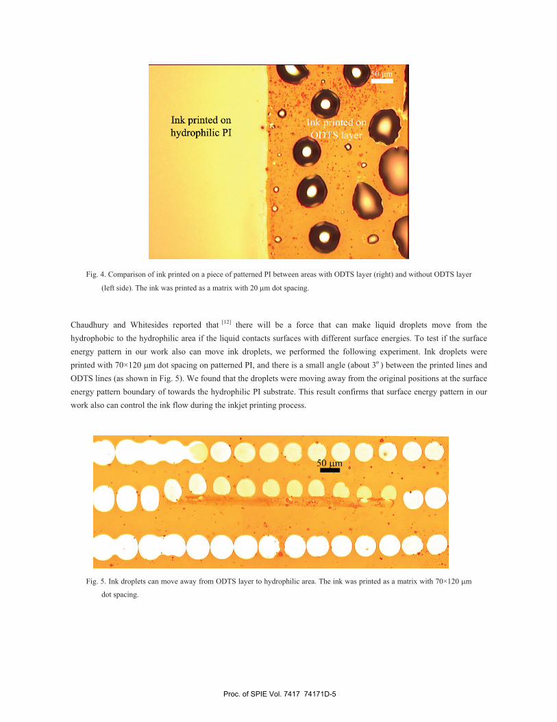
Fig. 4. Comparison of ink printed on a piece of patterned PI between areas with ODTS layer (right) and without ODTS layer
(left side). The ink was printed as a matrix with 20 �m dot spacing.
Chaudhury and Whitesides reported that [12] there will be a force that can make liquid droplets move from the hydrophobic to the hydrophilic area if the liquid contacts surfaces with different surface energies. To test if the surface energy pattern in our work also can move ink droplets, we performed the following experiment. Ink droplets were printed with 70×120 �m dot spacing on patterned PI, and there is a small angle (about 3 ) between the printed lines and ODTS lines (as shown in Fig. 5). We found that the droplets were moving away from the original positions at the surface energy pattern boundary of towards the hydrophilic PI substrate. This result confirms that surface energy pattern in our work also can control the ink flow during the inkjet printing process.
Fig. 5. Ink droplets can move away from ODTS layer to hydrophilic area. The ink was printed as a matrix with 70×120 �m
dot spacing.
Proc. of SPIE Vol. 7417 74171D-5

It is difficult to inkjet-print patterns with narrow gap on common substrates even all of the droplets printing very accurately.[13] The movement of the substrate during the inkjet process may also lead to printed ink flow and spread away from the desired position partially destroying the pattern. However, using our approach much thinner and smoother gaps can be easily obtained as seen in Fig. 6 (a) and (b). The silver ink was inkjet printed homogeneously in 20 �m dot spacing without any gaps, and by patterning ODTS lines on the substrate we can form 15 �m thin gaps in a controlled fashion. These lines are kept perfectly during possible movements of the substrate before the ink is dry, and the edge of thin gap can be much smoother than printed ink on polyimide without surface energy patterning. The AFM morphology figure in Fig. 6 (c) shows that both sides of the dried ink are higher than the ODTS line, which confirms that the ink was divided into two by the high surface energy contrast in inkjet printing process. It is impossible for a rough line on substrate to get such a printed quality only by the morphology.
Proc. of SPIE Vol. 7417 74171D-6

Fig. 6. Cabot ink (white) printed on patterned PI substrate with 15 �m ODTS lines observed by optical micrsocopy using (a)
5 times magnification and (b) 20 times magnification, as well as using (c) AFM.
4. CONCLUSION
In this work, an enhanced control of ink flow and spread in inkjet printing is obtained by surface energy patterning. We used it to improve the resolution of printed patterns. Hydrophobic ODTS pattern was deposited on a hydrophilic substrate by stamping firstly, and thereafter the silver ink was inkjet printed on top of the pattern. The ink droplets can move away from the hydrophobic layer to hydrophilic area. Thinner and smoother gaps (about 15 �m wide) were obtained easily by this method. This visible and easy processing surface energy pattern has its potential applications in smaller printed devices and high resolution integrated circuits.
5. ACKNOWLEDGMENTS
We acknowledge valuable discussion with T. Mäkelä, financial support from Tekes, through the PRINT project acknowledged.
REFERENCES
[1] Kawase, T., Shimoda, T., Newsome, C., Sirringhaus, H., and Friend, R. H., “Inkjet printing of polymer thin film transistors”, Thin Solid Films 438–439, 279–287 (2003).
[2] Shimoda, T., Morii, K., Seki, S., and Kiguchi, H., “Inkjet printing of light-emitting polymer displays”, MRS Bull. 28(11), 821-827 (2003).
[3] Subramanian, V., Chang, P. C., Lee, J. B., Molesa, S. E., and Volkman, S, K., “Printed organic transistors for ultra-low-cost RFID applications”, IEEE Trans. Compon. Packag. Tech. 28(4), 742-747 (2005).
[4] Sekitani, T., Zaitsu, K., Noguchi, Y., Ishibe, K., Takamiya, M., Sakurai, T., and Someya, T., “Printed Nonvolatile Memory for a Sheet-Type Communication System”, IEEE Trans. Electron 56(5), 1027-1035 (2009).
[5] Tekin, E., Smith, P. J., and Schubert, U. S., “Inkjet printing as a deposition and patterning tool for polymers and inorganic particles”, Soft Matter, 4(4), 703-713 (2008).
Proc. of SPIE Vol. 7417 74171D-7

[6] Sekitani, T., Noguchi, Y., Zschieschang, U., Klauk, H., and Someya, T., “Organic transistors manufactured using inkjet technology with subfemtoliter accuracy”, Proc. Natl. Acad. Sci. USA 105(13), 4976-4980 (2008).
[7] Wang, J. Z., Zheng, Z. H., Li, H. W., Huck, W. T. S., and Sirringhaus, H., “Dewetting of conducting polymer inkjet droplets on patterned surfaces”, Nature mater. 3(3), 171-176 (2004).
[8] Harada, Y., Girolami, G. S., and Nuzzo, R. G., “Growth kinetics and morphology of self-assembled monolayers formed by contact printing 7-octenyltrichlorosilane and octadecyltrichlorosilane on Si(100) wafers”, Langmuir 20(25), 10878-10888 (2004).
[9] Kumar, A., Biebuyck, H. A., and Whitesides, G. M., “Patterning Self -Assembled Monolayers: Applications in Materials Science”, Langmuir 10(5), 1498-1511 (1994).
[10] Inagaki,N., Tasaka,S., and Hibi, K., “Surface modification of Kapton film by plasma treatments”, J. Polymer Sci. Polymer Chem. 30(7), 1425 – 1431 (1992).
[11] Caglar, U., Kaija, K, and Mansikkamaki, P., “Analysis of mechanical performance of silver inkjet-printed structures”, Nanoelectronics Conference, INEC 2008. 2nd IEEE International, 851-856 (2008).
[12] Chaudhury, M. K. and Whitesides, G. M., “How to Make Water Run Uphill”, Science 256(5063), 1539-1541 (1992). [13] Stringer, J., and Derby, B., “Limits to feature size and resolution in inkjet printing”, J. Eur. Ceram. Soc. 29(5),
913-918 (2009).
Proc. of SPIE Vol. 7417 74171D-8
Related Documents