Surface Conduction Electron Surface Conduction Electron Emitter Display (SED) Emitter Display (SED)

Surface conduction electron emitter display (SED)
Jul 15, 2015
Welcome message from author
This document is posted to help you gain knowledge. Please leave a comment to let me know what you think about it! Share it to your friends and learn new things together.
Transcript
Surface Conduction Electron Surface Conduction Electron Emitter Display (SED)Emitter Display (SED)

INTRODUCTIONINTRODUCTION
The SED technology has been developing since The SED technology has been developing since 1987. The flat panel display technology that 1987. The flat panel display technology that employs surface conduction electron emitters for employs surface conduction electron emitters for every individual display pixel can be referred to as every individual display pixel can be referred to as The Surface-conduction Electron-emitter Display The Surface-conduction Electron-emitter Display (SED). Though the technology differs, the basic (SED). Though the technology differs, the basic theory that the emitted electrons can excite atheory that the emitted electrons can excite aphosphor coating on the display panel seems to be phosphor coating on the display panel seems to be the bottom line for both the SED display the bottom line for both the SED display technology and the traditional cathode ray tubetechnology and the traditional cathode ray tube(CRT) Televisions.(CRT) Televisions.

CRTCRT Highest image quality.Highest image quality. Costlier than most others.Costlier than most others.
LCDLCD Motion blurMotion blur.. Low power consumption.Low power consumption.
PLASMAPLASMA Grey levels are high.Grey levels are high. High power consumption.High power consumption.
Current display technologies

Manufacture of SED TVManufacture of SED TV
SED is a display device includes an electron-SED is a display device includes an electron-emitting device which is a laminate of an emitting device which is a laminate of an insulating layer and a pair of opposing insulating layer and a pair of opposing electrodes formed on a planar substrate.electrodes formed on a planar substrate. First the anode and cathode plates are First the anode and cathode plates are
fabricated separately.fabricated separately. Assembled with the other components.Assembled with the other components. Sealed using glass frit or other novel Sealed using glass frit or other novel
materials and then evacuated.materials and then evacuated.

Block diagramBlock diagram


WORKINGWORKING
CREATING THE PICTURECREATING THE PICTURE
Electrons are emitted from the electron Electrons are emitted from the electron emission region by applying a voltage to the emission region by applying a voltage to the electrodes, thereby stimulating a phosphorous to electrodes, thereby stimulating a phosphorous to emit light .emit light .
It's a flat-panel television that uses millions of It's a flat-panel television that uses millions of miniature CRTs are called Surface Conducting miniature CRTs are called Surface Conducting Electron emitters (SCEs). A set has three SCEs for Electron emitters (SCEs). A set has three SCEs for every pixel -- one each for Red, Green and Blue.every pixel -- one each for Red, Green and Blue.

A widescreen, high-definition set can have more A widescreen, high-definition set can have more than 6 million SCEs.than 6 million SCEs.
An SED-TV has millions of these SCEs arranged An SED-TV has millions of these SCEs arranged in a matrix, and each one controls the Red, in a matrix, and each one controls the Red, Green or Blue aspect of one pixel of the picture. Green or Blue aspect of one pixel of the picture.
The inside of an SED-TV is a vacuum. All of the The inside of an SED-TV is a vacuum. All of the SCEs are on one side of the vacuum, and the SCEs are on one side of the vacuum, and the phosphor- coated screen is on the other. The phosphor- coated screen is on the other. The screen has a positive electrical charge, so it screen has a positive electrical charge, so it attracts the electrons from the SCEs. attracts the electrons from the SCEs.

When bombarded by moderate voltages (tens of When bombarded by moderate voltages (tens of volts), the electrons tunnel across a thin slit in volts), the electrons tunnel across a thin slit in the surface conduction electron emitter the surface conduction electron emitter apparatus. apparatus.
Some of these electrons are then scattered at the Some of these electrons are then scattered at the receiving pole and are accelerated towards the receiving pole and are accelerated towards the display surface. These emitted electrons can then display surface. These emitted electrons can then excite the phosphor coating on the display panel. excite the phosphor coating on the display panel.
When they reach the screen, the electrons pass When they reach the screen, the electrons pass through a very thin layer of aluminum. They hit through a very thin layer of aluminum. They hit the phosphors, which then emit red, green or the phosphors, which then emit red, green or blue light.blue light.

Our eyes and brain combine these glowing dots Our eyes and brain combine these glowing dots to create a picture. Any part of the screen that's to create a picture. Any part of the screen that's not used to create pixels is black, which gives the not used to create pixels is black, which gives the picture better contrast. picture better contrast.
There's also a color filter between the phosphors There's also a color filter between the phosphors and the glass to improve color accuracy and cut and the glass to improve color accuracy and cut down on reflected light.down on reflected light.
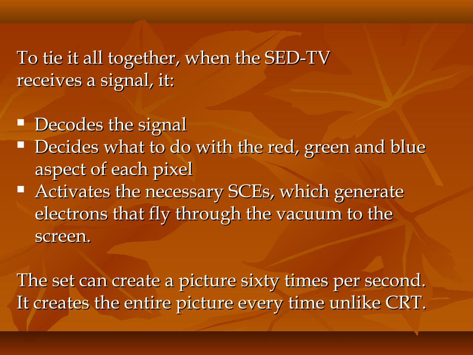
To tie it all together, when the SED-TV To tie it all together, when the SED-TV receives a signal, it:receives a signal, it:
Decodes the signalDecodes the signal Decides what to do with the red, green and blue Decides what to do with the red, green and blue aspect of each pixelaspect of each pixel Activates the necessary SCEs, which generate Activates the necessary SCEs, which generate electrons that fly through the vacuum to the electrons that fly through the vacuum to the screen.screen.
The set can create a picture sixty times per second.The set can create a picture sixty times per second.It creates the entire picture every time unlike CRT.It creates the entire picture every time unlike CRT.


FABRICATION OF NANO GAPSFABRICATION OF NANO GAPS
Nanogaps are the electron guns of SED.A Nanogaps are the electron guns of SED.A nanometer scale gap (nanogap) structure in nanometer scale gap (nanogap) structure in palladium strip fabricated by hydrogen palladium strip fabricated by hydrogen absorption under high-pressure treatment. absorption under high-pressure treatment.
It is found that the It is found that the edge roughness edge roughness of the nanogap of the nanogap improves the electron emission characteristics. improves the electron emission characteristics. The electron emission current is dependent upon The electron emission current is dependent upon the angle of inclination of surface.the angle of inclination of surface.

Hydrogen plasma treatment is used to increase Hydrogen plasma treatment is used to increase the edge roughness of the nanogap and thereby the edge roughness of the nanogap and thereby dramatically improve the electron emission dramatically improve the electron emission characteristics. For the nanogap with a separation characteristics. For the nanogap with a separation of 90 nm, the turn-on voltage significantly reduces of 90 nm, the turn-on voltage significantly reduces from 60 to 20 V after the hydrogen plasma from 60 to 20 V after the hydrogen plasma treatment.treatment.


Electrons are supplied to the anode Electrons are supplied to the anode in 2 stepsin 2 steps
Step 1Step 1: The electron source operates by first : The electron source operates by first emitting electrons laterally across a very emitting electrons laterally across a very narrow gap formed between two electrodes. narrow gap formed between two electrodes. The electrons tunnel through the vaccum gap The electrons tunnel through the vaccum gap from one electrode to the other electrode.from one electrode to the other electrode.
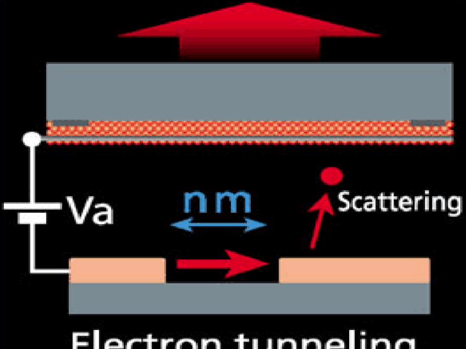
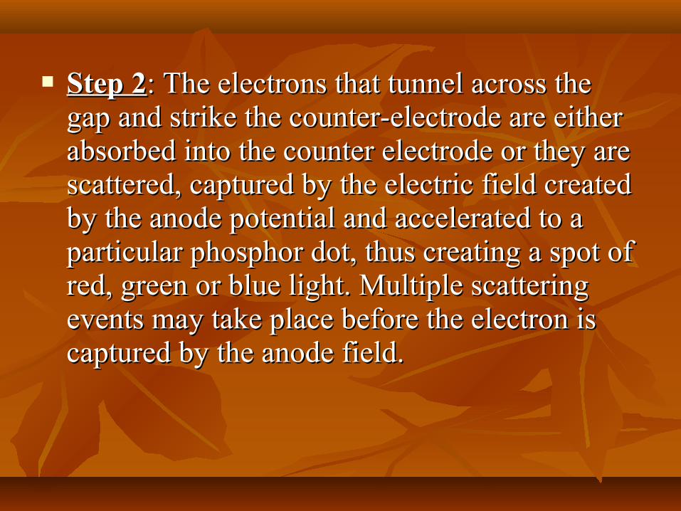
Step 2Step 2: The electrons that tunnel across the : The electrons that tunnel across the gap and strike the counter-electrode are either gap and strike the counter-electrode are either absorbed into the counter electrode or they are absorbed into the counter electrode or they are scattered, captured by the electric field created scattered, captured by the electric field created by the anode potential and accelerated to a by the anode potential and accelerated to a particular phosphor dot, thus creating a spot of particular phosphor dot, thus creating a spot of red, green or blue light. Multiple scattering red, green or blue light. Multiple scattering events may take place before the electron is events may take place before the electron is captured by the anode field.captured by the anode field.


SED TV Compared to CRTSED TV Compared to CRT
CRTCRT They are as deep as they They are as deep as they
are wide and they are are wide and they are heavy too.heavy too.
Have image challenges Have image challenges around the far edges of around the far edges of the picture tube.the picture tube.
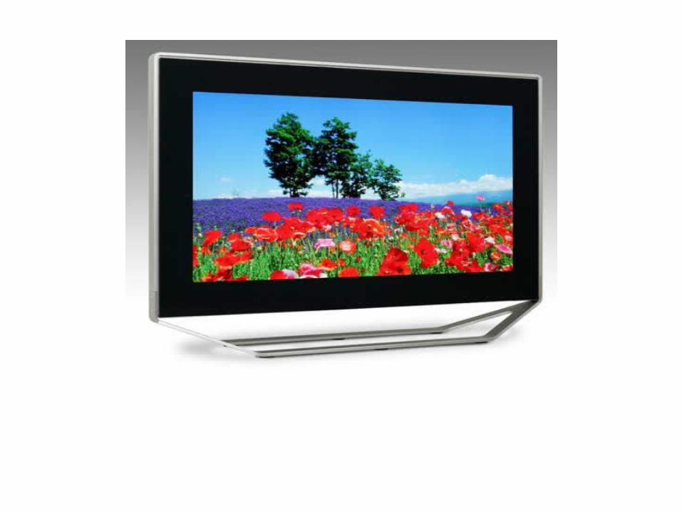
SEDSED They’re slim and light They’re slim and light
weight.weight.
CRTs can be made as CRTs can be made as large as the large as the manufacturer dares.manufacturer dares.

SED TV Compared to Plasma TV SED TV Compared to Plasma TV
Plasma TVPlasma TV
Grey levels in plasma TVs Grey levels in plasma TVs are high. The black is are high. The black is actually dark grey.actually dark grey.
Consumes more power.Consumes more power.
Suffers from black level Suffers from black level issues and solarization.issues and solarization.
SEDSED
Perfect black.Perfect black.
SEDs consumes half the SEDs consumes half the power that the plasma does power that the plasma does at the given screen size.at the given screen size.
SEDs don’t have such SEDs don’t have such issues.issues.
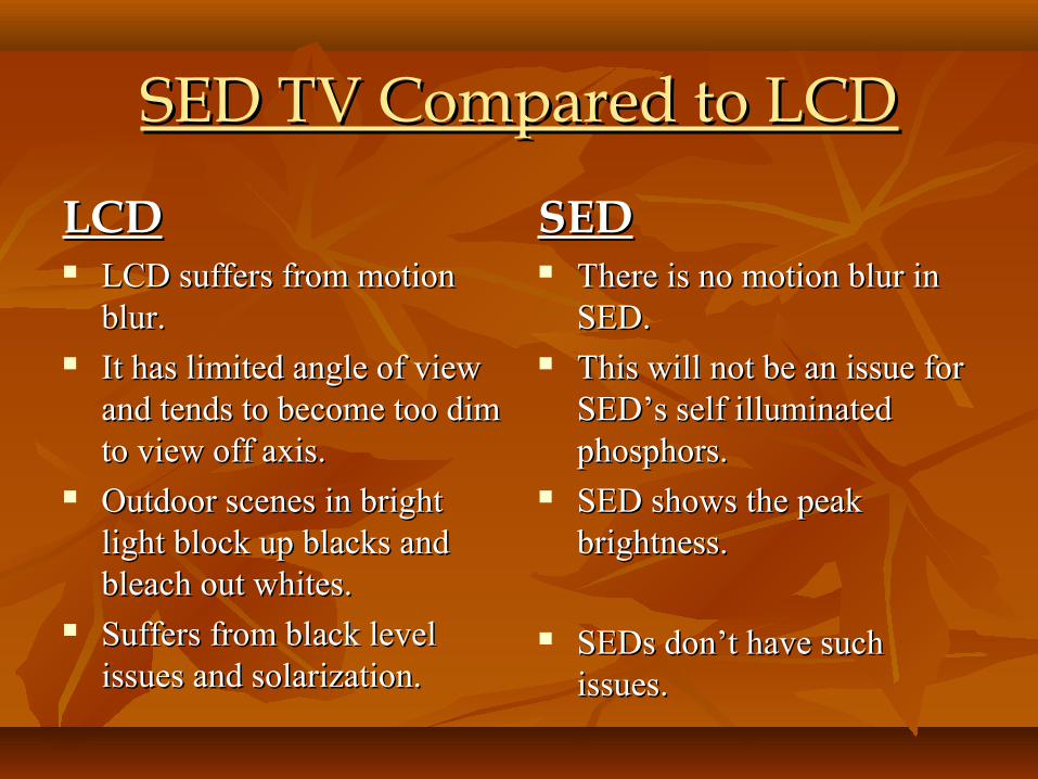
SED TV Compared to LCDSED TV Compared to LCD
LCDLCD LCD suffers from motion LCD suffers from motion
blur.blur. It has limited angle of view It has limited angle of view
and tends to become too dim and tends to become too dim to view off axis.to view off axis.
Outdoor scenes in bright Outdoor scenes in bright light block up blacks and light block up blacks and bleach out whites.bleach out whites.
Suffers from black level Suffers from black level issues and solarization.issues and solarization.
SEDSED There is no motion blur in There is no motion blur in
SED.SED. This will not be an issue for This will not be an issue for
SED’s self illuminated SED’s self illuminated phosphors.phosphors.
SED shows the peak SED shows the peak brightness.brightness.
SEDs don’t have such SEDs don’t have such issues.issues.

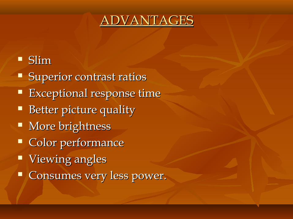
ADVANTAGESADVANTAGES
Slim Slim Superior contrast ratios Superior contrast ratios Exceptional response time Exceptional response time Better picture quality Better picture quality More brightnessMore brightness Color performanceColor performance Viewing anglesViewing angles Consumes very less power.Consumes very less power.

FEATURES FEATURES
Contrast ratio 100,000:1.Contrast ratio 100,000:1. Response time 0.2 milliseconds.Response time 0.2 milliseconds. Brightness of 450 cd/m2.Brightness of 450 cd/m2. 180º Viewing angle.180º Viewing angle. Viewable in Bright room.Viewable in Bright room. It can be used in Mobile device display.It can be used in Mobile device display. Low power consumption.Low power consumption. Longer life expectancy.Longer life expectancy.

CONCLUSIONCONCLUSION
SED will be the next generation display technology SED will be the next generation display technology in the near by future though patent controversy in the near by future though patent controversy and the lack of cheaper manufacturing techniques and the lack of cheaper manufacturing techniques are slowing down the commercial viability of are slowing down the commercial viability of SED TV.SED TV.

REFERENCEREFERENCE
www.canon.comwww.canon.com www.thoshiba.comwww.thoshiba.com www.electronics.howstuffworks.comwww.electronics.howstuffworks.com www.howstuffworks.comwww.howstuffworks.com www.wikipedia.comwww.wikipedia.com www.patentstorm.uswww.patentstorm.us www.freepatentsonline.comwww.freepatentsonline.com www.googlepatents.comwww.googlepatents.com

THANK YOU…THANK YOU…
Related Documents


