Surface & Coatings Technology 420 (2021) 127339 Available online 26 May 2021 0257-8972/© 2021 The Authors. Published by Elsevier B.V. This is an open access article under the CC BY-NC-ND license (http://creativecommons.org/licenses/by-nc-nd/4.0/). Hard Anodizing and Plasma Electrolytic Oxidation of an Additively Manufactured Al-Si alloy H. Mora-Sanchez a, *, 1 , R. del Olmo a, 1 , J. Rams b , B. Torres b , M. Mohedano a , E. Matykina a , R. Arrabal a a Departamento de Ingeniería Química y de Materiales, Facultad de Ciencias Químicas, Universidad Complutense, 28040 Madrid, Spain b Dpto. Matem´ atica Aplicada, Ciencia e Ingeniería de Materiales y Tecnología Electr´ onica, Universidad Rey Juan Carlos, C/Tulip´ an s/n, M´ ostoles 28933, Madrid, Spain A R T I C L E INFO Keywords: Additive Manufacturing Hard Anodizing Plasma Electrolytic Oxidation Tribology Aluminium Silicon ABSTRACT Plasma Electrolytic Oxidation (PEO) and Hard Anodizing (HA) coatings are investigated on an Additively Manufactured (AM) Al10Si1Mg alloy obtained via Direct Metal Laser Sintering (DMLS). Results are compared to those obtained for a conventional A361 cast alloy. Findings revealed that the microstructure of the AM alloy, consisting of α-Al cells enclosed in a Si network, produces coatings that are more uniform –in terms of morphology, thickness and roughness of the coating/substrate interface– than those obtained on the cast alloy. However, enhanced oxidation of the fine Si network in the AM alloy results in softer coatings. In both alloys, PEO coatings demonstrate superior wear protection than HA due to the presence of mullite in the former. The anisotropy in the microstructure of the AM alloy influences the tribological behaviour of studied coatings, with the XZ plane showing superior wear performance. 1. Introduction The use of aluminium alloys in the automotive, aeronautical and aerospace industries is widely extended. The interest of these industries in Additive Manufacturing (AM) processes to reduce fabrication opera- tions of complex shape components motivated the research on AM aluminium alloys [1]. Among the generally used alloys, the Al-Si alloys are the easiest to process by AM due to their optimal casting properties [2]. Direkt Metall Laser Schmelzen, or DMLS (direct metal laser melting in English), commonly termed as Direct Metal Laser Sintering, is a laser powder bed fusion (LPBF) AM technology that was developed and registered by EOS (Germany) [3–5]. It relies on a layer-by-layer melting of metallic powders by a high power laser [6]. In the DMLS processing, a laser scans a layer of metallic powder on the building platform following a pattern. Along its path, the laser melts the powder creating a melt pool which is subsequently solidified. Once a layer is consolidated, the building platform is lowered and the feeding system spreads a new layer of metallic powder. This process is repeated until the desired 3D part is obtained. DMLS and similar LPBF technologies, such as Selective Laser Melting (SLM), have the ability to obtain dense near-net-shape 3D metallic parts with high resolution and complex geometries including internal features [7–10]. The characteristics of DMLS in comparison with other AM technologies can be found in recent reviews [5,11]. Aluminium alloys are often surface treated by Hard Anodizing (HA) in sulphuric acid media to improve their corrosion resistance and tribological performance in wear-sensitive applications such as cylin- ders or pistons [12]. The mechanism involved in oxide growth during HA is almost the same as the one in conventional anodizing, although the higher concentration of sulphuric acid and current densities used in HA result in thicker, denser and harder oxide layers [13]. Coatings produced by Plasma Electrolytic Oxidation (PEO), also known as Micro-Arc Oxidation (MAO), have already demonstrated su- perior corrosion and tribological properties with respect to HA coatings as well as reducing the detrimental effect in the fatigue properties [13–15]. PEO is similar to conventional anodizing in terms of equipment and procedure, except for the substantially higher cell voltage [16–18]. Besides, HA requires the use of strong acids, which raises concerns about their application and disposal. By contrast, PEO is based on alkaline electrolytes free of heavy metals (e.g. Cr, V). The formation of new oxide/coating material during PEO occurs under the action of plasma micro-discharges across the forming coating rather than by continuous * Corresponding author. E-mail address: [email protected] (H. Mora-Sanchez). 1 Equally contributed. Contents lists available at ScienceDirect Surface & Coatings Technology journal homepage: www.elsevier.com/locate/surfcoat https://doi.org/10.1016/j.surfcoat.2021.127339 Received 13 January 2021; Received in revised form 27 April 2021; Accepted 20 May 2021

Welcome message from author
This document is posted to help you gain knowledge. Please leave a comment to let me know what you think about it! Share it to your friends and learn new things together.
Transcript

Surface & Coatings Technology 420 (2021) 127339
Available online 26 May 20210257-8972/© 2021 The Authors. Published by Elsevier B.V. This is an open access article under the CC BY-NC-ND license(http://creativecommons.org/licenses/by-nc-nd/4.0/).
Hard Anodizing and Plasma Electrolytic Oxidation of an Additively Manufactured Al-Si alloy
H. Mora-Sanchez a,*,1, R. del Olmo a,1, J. Rams b, B. Torres b, M. Mohedano a, E. Matykina a, R. Arrabal a
a Departamento de Ingeniería Química y de Materiales, Facultad de Ciencias Químicas, Universidad Complutense, 28040 Madrid, Spain b Dpto. Matematica Aplicada, Ciencia e Ingeniería de Materiales y Tecnología Electronica, Universidad Rey Juan Carlos, C/Tulipan s/n, Mostoles 28933, Madrid, Spain
A R T I C L E I N F O
Keywords: Additive Manufacturing Hard Anodizing Plasma Electrolytic Oxidation Tribology Aluminium Silicon
A B S T R A C T
Plasma Electrolytic Oxidation (PEO) and Hard Anodizing (HA) coatings are investigated on an Additively Manufactured (AM) Al10Si1Mg alloy obtained via Direct Metal Laser Sintering (DMLS). Results are compared to those obtained for a conventional A361 cast alloy. Findings revealed that the microstructure of the AM alloy, consisting of α-Al cells enclosed in a Si network, produces coatings that are more uniform –in terms of morphology, thickness and roughness of the coating/substrate interface– than those obtained on the cast alloy. However, enhanced oxidation of the fine Si network in the AM alloy results in softer coatings. In both alloys, PEO coatings demonstrate superior wear protection than HA due to the presence of mullite in the former. The anisotropy in the microstructure of the AM alloy influences the tribological behaviour of studied coatings, with the XZ plane showing superior wear performance.
1. Introduction
The use of aluminium alloys in the automotive, aeronautical and aerospace industries is widely extended. The interest of these industries in Additive Manufacturing (AM) processes to reduce fabrication opera-tions of complex shape components motivated the research on AM aluminium alloys [1]. Among the generally used alloys, the Al-Si alloys are the easiest to process by AM due to their optimal casting properties [2].
Direkt Metall Laser Schmelzen, or DMLS (direct metal laser melting in English), commonly termed as Direct Metal Laser Sintering, is a laser powder bed fusion (LPBF) AM technology that was developed and registered by EOS (Germany) [3–5]. It relies on a layer-by-layer melting of metallic powders by a high power laser [6]. In the DMLS processing, a laser scans a layer of metallic powder on the building platform following a pattern. Along its path, the laser melts the powder creating a melt pool which is subsequently solidified. Once a layer is consolidated, the building platform is lowered and the feeding system spreads a new layer of metallic powder. This process is repeated until the desired 3D part is obtained. DMLS and similar LPBF technologies, such as Selective Laser Melting (SLM), have the ability to obtain dense near-net-shape 3D
metallic parts with high resolution and complex geometries including internal features [7–10]. The characteristics of DMLS in comparison with other AM technologies can be found in recent reviews [5,11].
Aluminium alloys are often surface treated by Hard Anodizing (HA) in sulphuric acid media to improve their corrosion resistance and tribological performance in wear-sensitive applications such as cylin-ders or pistons [12]. The mechanism involved in oxide growth during HA is almost the same as the one in conventional anodizing, although the higher concentration of sulphuric acid and current densities used in HA result in thicker, denser and harder oxide layers [13].
Coatings produced by Plasma Electrolytic Oxidation (PEO), also known as Micro-Arc Oxidation (MAO), have already demonstrated su-perior corrosion and tribological properties with respect to HA coatings as well as reducing the detrimental effect in the fatigue properties [13–15]. PEO is similar to conventional anodizing in terms of equipment and procedure, except for the substantially higher cell voltage [16–18]. Besides, HA requires the use of strong acids, which raises concerns about their application and disposal. By contrast, PEO is based on alkaline electrolytes free of heavy metals (e.g. Cr, V). The formation of new oxide/coating material during PEO occurs under the action of plasma micro-discharges across the forming coating rather than by continuous
* Corresponding author. E-mail address: [email protected] (H. Mora-Sanchez).
1 Equally contributed.
Contents lists available at ScienceDirect
Surface & Coatings Technology
journal homepage: www.elsevier.com/locate/surfcoat
https://doi.org/10.1016/j.surfcoat.2021.127339 Received 13 January 2021; Received in revised form 27 April 2021; Accepted 20 May 2021

Surface & Coatings Technology 420 (2021) 127339
2
flow of ions as in anodizing. The presence of micro-discharges involves local high temperatures and pressures, which promote the formation of crystalline phases. During PEO, electrolyte-derived elements can be incorporated through plasma reactions, thus tailoring the properties of the coatings [19,20].
Although HA and PEO on Al alloys manufactured by conventional methodologies have been widely studied in the past [21–25], there are only a few recent studies on anodizing and PEO of AM Al-Si [14,26–28]. For instance, Revilla et al. [29–31] demonstrated that the microstruc-ture of AM Al-Si affected the growth mechanisms during conventional anodizing and the corrosion behaviour. To the best knowledge of the authors, in the only PEO study to date concerning AM alloys, Pezzato et al. [14] successfully produced corrosion resistant PEO coatings with different levels of porosity depending on the level of porosity of the substrate.
Cast Al-Si alloys are characterized by a bimodal microstructure with α-Al dendrites and a eutectic α-Al + Si aggregate [32,33]. The presence of Si crystals produces local current shielding during anodizing since Si requires higher voltages than Al to be oxidized [26]. This effect results in coatings with partially-oxidized Si particles and lower thickness at the eutectic regions. On the other hand, the AM Al-Si microstructure is characterized by a fine Si 3D network enclosing α-Al cells within the Melt Pool (MP) formed along the laser track [29]. An anisotropic macrostructure with respect to the XY and XZ planes (parallel and perpendicular to the building platform, respectively) is typically observed according to the relative direction of the MP [34]. Due to the lower cooling rate, the microstructure becomes coarser at the melt pool borders (MPBs), where the Si 3D network grows in size and inter-connectivity As shown by Revilla et al., during anodizing of AM Al-Si alloys, full oxidation of Si crystals is observed due to their small size and homogeneous distribution. As a result, more uniform and compact coatings are formed compared to the cast alloy, although the required anodizing voltages are higher and the growth rate decreases [31]. Anisotropic film growth on XY and XZ planes was also observed due to the dissimilar MPBs density encountered by the anodizing front.
These few existing studies have revealed significant effects of the AM Al-Si alloys microstructures on their anodizing and corrosion behav-iours. However, little is known on the wear behaviour of AM Al-Si alloys surface treated by Hard Anodizing and Plasma Electrolytic Oxidation. These two technologies are particularly well suited for surface modifi-cation of complex geometries, with PEO offering the advantage of more environmentally-friendly electrolytes.
In the present study, HA and PEO coatings are investigated on an Al- 10Si1Mg alloy fabricated by Direct Metal Laser Sintering (DMLS). The morphology, composition, mechanical properties and tribological per-formance of the modified surfaces are compared to those of a conven-tional cast Al-Si alloy. For the AM alloy, the effect of the macro/micro-
anisotropy between XY and XZ planes on the resultant coatings is also investigated.
2. Materials and experimental procedures
2.1. Cast and AM Al-Si alloy
A cast A361 alloy (Si, 10.50 wt%; Fe, 0.53 wt%; Mg, 0.36 wt%; Mn, 0.12 wt%; Zn, 0.11 wt%; Cu, 0.1 wt%; and Al, balance. Duralcan, USA) was used as a reference material. Specimens of 30 × 10 × 5 mm were cut from a large ingot. The AM Al10Si1Mg alloy fabricated via DMLS (M280 EOS, EOS, Germany) was supplied by Fundacion Idonial (Asturias, Spain) in the form of 30 × 30 × 30 mm cubes. The AM alloy had a similar composition to the cast alloy and the powder feedstock had particle size in the range between 20 and 63 μm. The heat source was a laser with a power of 370 W and a spot size of 0.07 mm. The scan speed, layer thickness and hatching space were 1300 mm/s, 0.03 mm and 0.09 mm, respectively. The laser followed a default 5 mm “stripe hatching pattern” over the printing surface as depicted in Fig. 1a. The laser swept the stripes via alternating scans orthogonal to the main stripe direction maintaining the hatching space between scans. The scanning layout was maintained for the subsequent layers but applying a 67◦ rotation with respect to the previous layer in order to minimize residual stresses. Immediately after the DMLS processing, the alloy was subjected to a stress-relief thermal treatment at 300 ◦C for 2 h followed by furnace cooling. 30 × 10 × 2 mm specimens were cut from the AM cubes in both XY and XZ orientations (Fig. 1b).
For metallographic characterization, the specimens were wet ground through successive grades of SiC abrasive papers from P120 to P1200. This was followed by 1 μm diamond polishing and etching in Keller reagent (nitric acid, 5 mL; hydrochloric acid, 3 mL; hydrofluoric acid, 2 mL; deionized water, 190 mL) for ~30 s.
2.2. Surface treatments
Prior to the anodizing treatments, the samples were wet ground with SiC abrasive papers from P120 to P1200 grade. A shielded copper wire was attached to the specimens to provide the electrical connection and a 2.4–3 cm2 working area was delimited using a commercial stopping-off resin (Lacquer 45, MacDermid plc). The thickness of the resulting coatings was measured with an eddy-current meter (ISOSCOPE FMP10, Fischer), equipped with an FTA3.3H probe, taking an average of 10 measurements.
2.2.1. Hard Anodizing – HA HA coatings were fabricated in a sulphuric acid aqueous solution
(200 g L− 1; PanReac AppliChem, 95–98%) in a 2 L double-walled glass
Fig. 1. (a) Scanning strategy during the DMLS process and (b) specimen extraction for XY and XZ orientations.
H. Mora-Sanchez et al.
Surface & Coatings Technology 420 (2021) 127339
3
cell at a constant current density of 20 mA cm− 2 provided by a DC power supply (SM400-AR-8, Delta Elektronika). A pure aluminium plate was used as a counter-electrode. The electrolyte was in continuous agitation at 300 rpm and maintained at a temperature of 273 K. The HA treatment times were adjusted for each alloy (i.e. A361 cast alloy and both XY and XZ planes of the AM alloy) in order to obtain a target thickness of approximately 70 μm were as follows: 5300 s, 6000 s and 6800 s for the A361, AMXY and AMXZ samples, respectively. The evolution of the coating thickness with the treatment time can be found in Supplemen-tary Fig. S1.
2.2.2. Plasma Electrolytic Oxidation – PEO PEO was carried out in a sodium silicate electrolyte (Na2O(SiO2)
x⋅xH2O, ≥27% SiO2, ρ = 1.39 kg dm− 3, 10.5 g L− 1; KOH, 2.8 g L− 1). The electrolyte was continuously stirred during the treatment at 300 rpm in a 2 L double-walled glass cell using a stainless steel plate (AISI 316L) as counter-electrode. The electrical signal applied consisted of a square signal (+490 V/− 110 V, 50% duty cycle and 50 Hz) with an initial voltage ramp of 60 s. The maximum current density was limited to 500 mA cm− 2. The PEO treatments featured the establishment of a “soft- sparking” regime which was accompanied by a characteristic current drop when the set voltage was reached (~2000 s) [35]. PEO treatments were stopped ~600 s after the current drop which ensured uniform ~70 μm thick coatings as a minimum. The evolution of the coating thickness with the treatment time can be found in Fig. S1. Note that the longest PEO treatment times presented in Fig. S1 ensured the homogeneous “soft sparking” regime as depicted by micrographs.
2.3. Microstructural characterization
Microstructural characterization of the bare alloys and cross-sections of coated specimens was performed by optical microscopy (Leica- Reichert MEF4 A/M) and Scanning Electron Microscopy (SEM, JEOL JSM-6400). The analysis of the composition was carried out via Energy Dispersive X-Ray Spectroscopy (EDS). The preparation of the bare alloys for microstructural characterization was performed as detailed in Sec-tion 2.1. To characterize the cross-section of the coatings, the specimens were embedded in a MA2+ commercial epoxy resin followed by SiC abrasive grinding and subsequent diamond polishing to 1 μm. The for-mation of crystalline phases in the coatings was assessed by Grazing Incidence X-Ray Diffraction (GIXRD, PANalytical X'Pert diffractometer, Cu Kα = 1.54056 Å) to maximize the contribution from the films. The diffractograms were obtained in the range from 10◦ to 60◦ (in 2θ) with a step size of 0.04◦ at incident angle of 0.5◦. The approximate penetration of the X-rays was below 5 μm for alumina density values of 4.05 g/cm3
(crystalline) and 2.66–3.4 g/cm3 (amorphous).
2.4. Mechanical properties
2.4.1. Hardness and elastic modulus The hardness (H) and elastic modulus (E) of the coatings were
measured by nanoindentations on the cross section of the coatings with a standard Berkovich tip in load control mode up to a maximum load of 100 mN. H and reduced E were calculated from the load-displacement curves following the Oliver and Pharr methodology [36]. The Pois-son's coefficients to calculate the E were 0.34 for Al [37] and 0.22 for Al2O3 [38]. 10 indentations per sample were performed at approxi-mately half of the coatings thickness and with a separation of 50 μm between each other to avoid interference from previous plastic deformation.
2.4.2. Sliding wear tests The tribological properties of HA and PEO coatings were evaluated in
dry conditions on a MT/60/NI ball-on-disc tester (MicroTest) at room temperature (~21 ◦C) and ~35% humidity. Tests were performed in ball-on-flat linear reciprocating mode. The coatings served as the plates
and the counterpart was a WC ball of 6 mm in diameter and 1800 HV hardness. The tests were carried out at a sliding speed of 40 mm/s for a maximum sliding distance of 70 m with a stroke length of 10 mm. Two sets of experiments were performed varying the normal load from 5 to 10 N. At least three wear tests were performed for each specimen and normal load.
To carry out the wear tests, the outer layer of the as-formed coatings was removed by grinding with a P320 SiC abrasive paper in order to obtain a flat and smooth surface, maintaining a nominal thickness for the wear tests of ~50 μm. This procedure eliminates the surface im-perfections of HA coatings and the outer porous layer of the PEO coat-ings [35].
The wear rates (Wr) were estimated dividing the wear volume (Wv) by the normal load applied and total sliding distance. The Wv was measured by high resolution 3D measurements (InfiniteFocusSL, Bruker Alicona) of the worn surfaces. For each test, a 3D reconstruction was obtained. The volume inside the wear track below the adjacent surface was considered as the Wv which was used to estimate the Wr of each test. The final Wr was the average of the three tests per specimen and loading condition. The friction coefficients (Fc) were acquired during the tests every 2 mm over 20 mm. Further, the data collected along the 20 mm was smoothened and averaged to provide a single value every 2 m. Worn surfaces were examined by SEM in order to identify the dominant wear mechanisms.
3. Results
3.1. Characterization of A361 cast and AM alloys
Fig. 1 shows the optical micrographs of the A361 cast alloy (Fig. 1a and b) and XY and XZ planes of the AM alloy (Fig. 1c and d). The A361 cast alloy presented the characteristic α-Al dendrites and α-Al + Si eutectic at the interdendritic spaces. Needle-shaped particles with high Fe content, possibly corresponding to β-AlFeSi intermetallics [33] were also found (Figs. 2b and 3). EDS maps also revealed the segregation of Mg suggesting the formation of other intermetallics such as π-AlFeSiMg and Mg2Si (Fig. 3d).
The microstructure of the DMLS Al-Si alloy is strongly determined by the melting of the powder during the pass of the laser. This creates a melt pool (MP) that subsequently solidifies at an extremely high rate [9,39]. The MPs, delimited by melt pool borders (MPB), were clearly visible by optical microscopy in both XY (Fig. 2c) and XZ (Fig. 2d). Due to the layer-by-layer manufacturing, the DMLS alloy was characterized by a strong macrostructural anisotropy: the MPs were elongated in the XY plane (Fig. 2c) while their transverse section was observed in XZ plane forming a scale-like macrostructure (Fig. 2d). SEM micrographs (Fig. 4) revealed that the microstructure of the DMLS Al-Si alloy consisted of α-Al cells enclosed in a 3D Si network (brighter phase). Within the MPs α-Al cells were globular in the XY plane (Fig. 4b) and elongated in the XZ plane (Fig. 4e) as a result of the directional solidification during the AM process [34]. The fine microstructure became coarser at the MPBs (Fig. 4c and f); this typically makes them visible in the optical micro-scope (Fig. 2c and d).
3.2. Fabrication of HA and PEO coatings
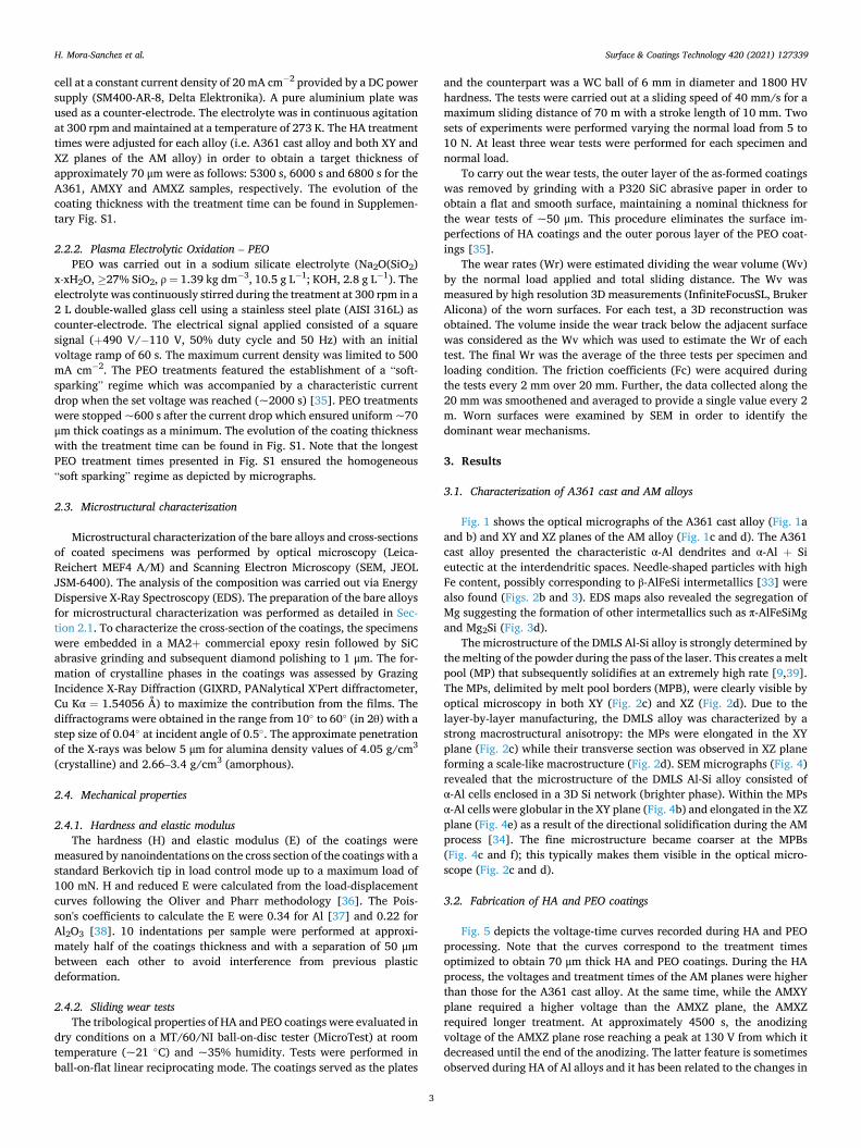
Fig. 5 depicts the voltage-time curves recorded during HA and PEO processing. Note that the curves correspond to the treatment times optimized to obtain 70 μm thick HA and PEO coatings. During the HA process, the voltages and treatment times of the AM planes were higher than those for the A361 cast alloy. At the same time, while the AMXY plane required a higher voltage than the AMXZ plane, the AMXZ required longer treatment. At approximately 4500 s, the anodizing voltage of the AMXZ plane rose reaching a peak at 130 V from which it decreased until the end of the anodizing. The latter feature is sometimes observed during HA of Al alloys and it has been related to the changes in
H. Mora-Sanchez et al.

Surface & Coatings Technology 420 (2021) 127339
4
Fig. 2. Optical micrographs of the samples: a–b) A361 cast alloy; c) XY plane of the AM alloy; and d) XZ plane of the AM alloy.
Fig. 3. a) SEM image of the A361 cast alloy. Images b), c) and d) correspond to Si at.%, Fe at.%, and Mg at.% EDS maps, respectively, taken at the area shown in a).
H. Mora-Sanchez et al.

Surface & Coatings Technology 420 (2021) 127339
5
film morphology (i.e. sponge-like or columnar) and thickness of the barrier layer [40], e.g. a thicker barrier layer is related to higher voltages.
During PEO, the A361 reached the formation voltage of 340 V after ~1200 s, whereas the AM specimens reached it later at ~2250 s, after a plateau at ~324 V. The higher voltage of the A361 alloy at the early stages indicate a higher coating resistance, which is possibly due to an increased thickness and density of the coating over the entire specimen surface [14,35]. Unlike the HA coatings on the AM alloy, no anisotropy during the PEO process was observed between AM planes.
3.3. Microstructural characterization of HA and PEO coatings
Fig. 6 depicts SEM and EDS Si maps of the HA and PEO coatings. These images revealed that the morphologies of the A361-HA (Fig. 6a–c) and AM-HA (Fig. 6d–f) coatings were clearly different. The A361-HA coating presented signs of partially oxidized Si crystals and
intermetallics within the coating (Table 1, measurements 2 and 3) and a hampered interface at the Si-rich eutectic regions of the material (Fig. S2a). The large size of the Si crystals at these eutectic regions impeded the complete anodization of the substrate and shielded the material beneath them. As a result, these sections of the coating were thinner and heterogeneous [31]. Porosity at these sections was linked to the formation of cavities by oxygen gas evolution during Si oxidation [41]. Further cavities might be formed via release of localised thermal and/or volume expansion stresses around the Si particle [30,42]. Detachment of large particles could also take place during metallo-graphic preparation. In contrast, thicker and compact regions of the A361-HA coating corresponded to anodized α-Al dendrites (Table 1; location 1).
The AM-HA coatings were more compact (i.e. less porosity) and had a flat coating-substrate interface. Si maps showed the homogeneous distribution of Si with an average content of 5.3 at.% (Fig. 6f, Table 1). These morphological and chemical features were the result of the fine Si-
Fig. 4. SEM images of the AM alloy: a–c) XY plane and d-f) XZ plane. Images b–c) and e–f) correspond to high magnification images taken at the areas shown in image a) and d), respectively. Images b) and e) were taken within the MP. Images c) and f) correspond to high magnification images at the MPB.
H. Mora-Sanchez et al.
Surface & Coatings Technology 420 (2021) 127339
6
network that led to the complete oxidation of Si [26,30]. MPBs produced certain heterogeneities in the morphology and retraced interface due to the coarser size of Si crystals (Fig. S2b and c). Cracks observed in the HA coatings were mainly formed during the metallographic preparation of the samples, i.e. sectioning and grinding, although some of the cracks are presumably due to thermal stresses induced by Joule effect and stresses generated by the growth of the oxide.
The PEO coatings on both A361 and AM alloys showed a high density of micro and sub-micro pores and cracks associated with gas evolution and thermal stresses induced by the micro-discharges, respectively (Fig. 6g–l) [14]. The A361-PEO coating appeared to have finer porosity than the AM-PEO coatings, although scattered and relatively large pores were visible in some areas. Image analysis revealed 4.6% porosity for the A361-PEO and 7.3% for the AM-PEO coatings. The coating-substrate interface was found flatter in the AM-PEO samples probably due to the fine distribution of Si (Fig. 6k), while the shielding effect of large Si crystals thinned the PEO coating over the eutectic regions of the cast alloy (Figs. 6h and i, S2). Nevertheless, the retrace of the coating- substrate interface in the A361-PEO specimen was less accentuated than in the case of the A361-HA probably due to the more aggressive character of plasma discharges. For both A361-PEO and AM-PEO coat-ings, Si was found to be preferentially located in the upper part of the coating due to the incorporation of electrolyte Si-rich species (Fig. 6i and l, Table 1). According to the EDS results presented in Table 1, the Si content in the AM-PEO specimens was slightly higher than for A361- PEO coating.
The XRD patterns of the bare substrates and HA-coated and PEO- coated samples are presented in Fig. 7a–c, respectively. Non-treated specimens revealed Al (ICDD card 00-004-0787) diffraction peaks at ~38◦ and ~45◦ and a weaker peak at ~28◦ corresponding to Si (ICDD card 00-027-1402) which was observed as a defined peak in the A361 sample and as a wide band in the AM samples. This is in agreement with the size of the Si particles for both alloys. No substantial differences between both AM planes were observed. It is worth noting that no contribution from Fe-containing intermetallics was found in the XRD pattern of the A361 cast alloy due to the limitations of the technique. This phase is only observed by X-ray when its content is significant. The full crystallographic characterization of these particles requires the use of more advanced techniques such as transmission electron microscopy (TEM) [33] or X-ray fluorescence spectroscopy (XRF) [43]. Neverthe-less, the nature of these Fe-rich needle or plate shaped particles in Al-Si alloys has been already well studied and is typically assigned to β-AlFeSi intermetallics [44].
The XRD patterns of the HA-coated samples revealed the presence of Al, indicating that the X-Ray beam reached the substrate, and a wide band between 20 and 35◦ (Fig. 7 b). The fact that substrate XRD peaks are detected is probably related to the inherent porosity of the coatings and/or some edge effect (coating damage due to cutting of the spec-imen). This wide band, together with the high Al content (Table 1), suggested that the HA coatings consisted mainly of amorphous alumina [13,41]. A strong Si diffraction peak appeared in the A361-HA probably due to a combined contribution from the Si in the substrate and the non- oxidized particles within the coating. Interestingly, no SiO2 diffractions were observed which could be linked to the large size of the Si particles preventing their oxidation. No clear Si diffraction peaks were observed in the AM samples which could be attributed to the overlapping of the weak wide band observed in Fig. 7a with the alumina-related band. On the contrary, the finer and homogeneous distribution of Si in the AM samples eased its oxidation leading to the formation of SiO2 (ICDD card 00-047-1301, Fig. 7b) [26]. A significant difference regarding the rela-tive intensity of SiO2 was observed between the HA coatings formed in both AM planes having the AMXZ-HA a greater signal than the AMXY- HA.
The XRD measurements of the PEO samples (Fig. 7c) revealed the presence of mullite (Al2O3⋅SiO2, ICDD card 01-079-1450). The wide band between 20 and 30◦ associated with amorphous Al2O3 had a sig-nificant presence in the A361-PEO and AMXZ-PEO samples while it was absent in the AMXY-PEO sample. The A361-PEO coating did not present substrate diffractions and the amorphous presence was more evident than in the AM specimens, which could indicate that the alumina on the AM-PEO coatings had a stronger amorphous character. SiO2 diffractions were only found in the AM-PEO specimens which was in agreement with the fact that the finer distribution of Si eased its oxidation and incor-poration into the coating. Anisotropy between AMXY-PEO and AMXZ- PEO specimens was observed in terms of intensity of the SiO2 diffrac-tions and the amorphous alumina wide band. It is worth recalling that according to the Si maps in Figs. 6i and 4l, Si-related crystalline phases should have formed preferentially at the outer layers of the PEO coatings.
3.4. Mechanical properties
3.4.1. Hardness and elastic modulus Fig. 8a depicts representative examples of load vs. displacement
curves of the nanoindentations performed on the bare alloys and the HA- and PEO-coatings, demonstrating the different mechanical behaviour of
Fig. 5. Voltage-time responses during HA and PEO treatments of A361 and XY and XZ planes of AM alloy and representative photographs of a AMXZ specimen before surface treatment and after HA and PEO treatments.
H. Mora-Sanchez et al.

Surface & Coatings Technology 420 (2021) 127339
7
the tested specimens. Fig. 8b shows the comparison of the average H and E values for each specimen calculated from the corresponding curves. AM substrates were slightly harder (1–2 GPa) and approximately seven times stiffer (~75 GPa) than the A361 specimen (0.5 and 10 GPa,
respectively). Regarding the response of the HA treated specimens, it appeared that the 3D SiO2 network developed within the AM-HA led to higher E (~55 GPa) than the A361-HA (26 GPa). The average H value of the AM-HA coatings was in the 2–3 GPa range and that of the A361-HA specimen was slightly higher (~4 GPa). In comparison with the bare substrates and amorphous HA coatings, the PEO coatings showed higher H and E. The A361-PEO specimen showed higher H and E (15 GPa and ~180 GPa, respectively) than the AM-PEO specimens (6 GPa and ~105 GPa, respectively).
3.4.2. Tribological properties The friction coefficients (Fc) measured for the un-treated substrates,
HA- and PEO-coated samples are shown in Fig. 9a, b, and c, respectively. Note that the first data point of the series corresponds to the first 2 m. The Fc of the substrates decreased with the wear distance (Fig. 9a). The initial values were between 0.8 ± 0.2 and 1.0 ± 0.3 for the A361 alloy at both loads and for both AM planes at 5 N, while for both AM planes at 10 N were at 0.60 ± 0.09. The values of the cast alloy decreased almost linearly to ~0.65 ± 0.02 at the end of the tests. For the AM alloy the Fc
Fig. 6. SEM micrographs of the cross-section of the coatings. First column: Overview of the cross-section. Second column: high magnification image of the area depicted in the first column. Third column: Si at.% EDS map of the area shown in the second column. a–f) HA coatings. g–l) PEO coatings. A361 alloy: a–c and g–i. AM alloy: d–f and j–l.
Table 1 Results of the local EDS measurements performed over the areas depicted in Fig. 6. All the results are given in at.%.
Coating Location O Na Al Si S K Fe
A361-HA 1 60.2 – 34.1 0.7 5.0 – – 2 57.1 – 21.8 17.4 3.2 – 0.5 3 50.4 – 25.0 19.0 2.9 – 2.8
AM-HA 1 54.6 – 35.3 5.3 4.8 – – A361-PEO 1 57.1 – 30.4 10.5 1.0 1.0 –
2 58.2 – 38.2 3.0 0.2 0.4 – 3 58.9 – 38.1 1.9 0.6 0.5 –
AM-PEO 1 54.2 0.8 26.0 15.8 – 3.1 – 2 52.0 0.2 41.9 4.8 – 1.1 – 3 48.9 0.6 39.1 8.6 – 2.8 –
H. Mora-Sanchez et al.

Surface & Coatings Technology 420 (2021) 127339
8
reached a steady state beyond 30 m. The final Fc of the AM samples at 10 N were lower (0.4 ± 0.09) than the ones at 5 N (~0.55 ± 0.06). The cast alloy presented large oscillations in contrast to the smoother evo-lution of the AM samples. This might be related to their more
homogeneous microstructure. The Fc of the HA-coated specimens reached a plateau after a running-
in period (Fig. 9b). The running-in period was larger for the A361-coated sample at both loads reaching the plateau at ~0.75 ± 0.07 after a wear distance of 25 m. The AM-coated samples presented a significantly shorter running-in period reaching the steady-state at approximately 10 m for both loads. This shorter running-in period might be related with the more homogeneous microstructure of the AM-HA samples. These samples also presented a clear load dependence being the Fcs 0.75 ±0.05 at 5 N and 0.80 ± 0.06 at 10 N. The PEO samples on the other hand, experimented a steady-state at about 0.65 ± 0.07 for almost the entire tests at both loads (Fig. 9c).
The calculated wear rates (Wr) of the bare alloys and coated speci-mens are shown in Fig. 10. These results demonstrate the benefit of HA and PEO treatments in the wear performance of the alloys with respect to the untreated specimens; the Wr values were reduced at both loads by at least one order of magnitude from >10− 3 mm3 N− 1 m− 1 (Fig. 10a) down to values <2 ⋅ 10− 4 mm3 N− 1 m− 1 (Fig. 10b). The reduction was especially significant in the case of the cast alloy; Wr was reduced from ~4 ⋅ 10− 3 mm3 N− 1 m− 1 to about 7.5 ⋅ 10− 6 mm3 N− 1 m− 1 for both treatments and loads.
Similarly to the Fc, the AM-coated samples showed a clear load dependence being the Wr greater for the 10 N tests. The HA treatment of the AM alloy showed a reduction of the Wr of about one order of magnitude (1–2 ⋅ 10− 4 mm3 N− 1 m− 1) with respect to the bare alloy (1–4 ⋅ 10− 3 mm3 N− 1 m− 1). Interestingly the AMXZ-HA coating pre-sented at 5 N the lowest Wr of the AM HA-coated samples: 1.5 ⋅ 10− 5
Fig. 7. Grazing angle X-Ray diffraction patterns. a) bare alloys; b) HA-coated specimens; and, c) PEO-coated specimens.
Fig. 8. a) representative load vs. displacement curves of the nanoindentations performed on all the specimens. b) Hardness (H) and the elastic modulus (E) values of bare alloys, HA-coated and PEO-coated A361 and AM planes.
H. Mora-Sanchez et al.

Surface & Coatings Technology 420 (2021) 127339
9
mm3 N− 1 m− 1. The Wr of the PEO-coated AM alloy were found between 0.8 ⋅ 10− 5 and 1.3 ⋅ 10− 5 mm3 N− 1 m− 1, except for the AMXY-PEO specimen which showed a slightly greater Wr of 2.7 ⋅ 10− 5 mm3 N− 1
m− 1. These results indicated that for any treatment and applied load, the AMXZ plane showed superior wear performance than the AMXY plane. It could be concluded that the treated samples showed better wear
performance in the following order: A361-PEO > A361-HA > AMXZ- PEO > AMXY-PEO > AMXZ-HA > AMXY-HA. This is mostly in accor-dance to the tendency observed for the H measurements (Section 3.4.1).
The backscattered SEM images of the wear tracks on the HA-coated specimens at 10 N are shown in Fig. 11. The differences between samples in the wear track width (Fig. 11a–c) were evident and in good agreement with the Wr trend shown in the previous section: A361-HA < AMXZ-HA < AMXY-HA. At higher magnification, it was observed that the wear surface on the A361-HA sample consisted entirely on a smooth and cracked tribolayer (Fig. 11d). For the AM-coated samples the wear track showed a rougher surface and isolated tribolayer islands with sharp edges (Fig. 11e and f). These tribolayer islands corresponded to darker areas in the wide plain views of the track in Fig. 11b and c. Similar to the A361-HA specimen, cracks were observed in the AM-coated samples in both detached areas and tribolayer islands.
Cross-section images showed the curved surface of the coatings after the wear tests (Fig. 11g-i). The top part of the coatings on the AM specimens at the wear track had a saw-like profile corresponding to the detached areas. At the top of the AMXY-HA cross-section a plate-like particle could be observed which would correspond to the tribolayer islands observed at the surface. Through-thickness cracks were found in the AMXY-HA sample and they could be found aligned with the sharp edges of the tribolayer island. Horizontal cracks under the tribolayer plate suggested that these would have grown beneath the tribolayer via shear forces producing the subsequent detachment by tension due to the stylus passing-over. No through-thickness cracks could be found in the AMXZ-HA specimen. Local EDS measurements (marks in Fig. 11g and h) did not reveal any presence of W, suggesting no transfer of the WC counterpart into the tribolayer. It is worth noticing that cracking outside the worn surface is also observed as a consequence of the stresses induced by the nearby sliding counterpart. It is believed that the existing residual stresses in the HA coatings significantly contribute to this cracking phenomenon. Residual stresses coming from the underlying substrate should be less relevant as the alloys were subjected to stress- relief thermal treatments.
The backscattered SEM images of the wear tracks on the PEO-coated specimens tested at 10 N load are shown in Fig. 12. The width of the wear tracks maintained the same trend observed in the Wr results: AMXY-PEO > AMXZ-PEO > A361-PEO. All the specimens presented the same smooth and sharp flake-like wear surface without significant detachment (Fig. 12d–f). At high magnification, the backscattered im-ages revealed some contrast within the track. EDS measurements (marked in Fig. 12d–f) showed traces of W at the brighter areas, indi-cating the damage of the WC counterpart and its transfer to the
Fig. 9. Friction coefficients during reciprocating wear tests at 5 and 10 N. a) bare alloys; b) HA-coated specimens; and, c) PEO-coated specimens.
10-6
10-5
10-4
10-3
10-2
10 N
5 N
PEOHA
mm(
rW
3·N
-1·m
-1)
Bare alloys
AMXY
A361
AMXZ
Fig. 10. Estimated Wr for the bare alloys, HA- and PEO-coated specimens after reciprocating sliding tests for a total sliding distance of 70 m at 5 and 10 N.
H. Mora-Sanchez et al.

Surface & Coatings Technology 420 (2021) 127339
10
tribolayer (Table 2). Cross-section SEM images did not reveal significant surface curvature at the wear locations. However, a fine brighter layer was found at the top of these regions corresponding to the W-rich tri-bolayer (Fig. 12g–i). Measurements confirming the content of W are shown in Table 2.
4. Discussion
4.1. Effect of the fine Si distribution in AM alloy on the HA and PEO processes
The microstructure of the AM Al-Si alloy consisted on a fine Si- network enclosing α-Al cells within the MPs. The microstructure became coarser at the MPBs as a result of the thermal gradient during the laser pass, increasing the interconnectivity of the Si- network. This characteristic microstructure influenced the HA and PEO processes and, in turn, the morphology and phase composition of the resulting coatings with respect to the A361 cast alloy. The AM alloy demonstrated anisotropy between the XY and XZ planes for both HA and PEO treat-ments regarding the phase composition and subsequent wear performance.
Hard Anodizing of the AM alloy required higher anodizing voltages than the A361 cast alloy due to the complete oxidation of Si, which was favoured by its finer grain size [31]. This, together with the homoge-neous distribution of this element, led to more homogeneous and compact HA coatings and the formation of crystalline SiO2 (Fig. 7b). The morphology of the AM-HA coatings could then be described as amor-phous alumina cells encapsulated in a crystalline 3D silica network.
The anisotropic anodizing of the AM alloy was already reported by Revilla and co-workers [26] who associated it with the different distri-bution of MPBs at the XY and XZ planes. For a better understanding, a schematic is presented in Fig. 13, which represents a simplified view of the AM microstructure, where MPBs are represented as white lines, and red and green lines represent the anodizing front advancing parallel to the XY and XZ planes, respectively. Two different situations should be considered: XZ) the anodizing front advances along the MPs, across elongated α-Al cells, with MPBs being mostly perpendicular to it; and, XY) the anodizing front moves across the MPs periodically going through coarse MPBs. Due to the coarser character of the MPBs, the XY anodizing front would alternate Si-rich layers which are more resistive than the MPs. This would increase the required anodizing voltage for the XY plane in comparison to the XZ plane.
XRD measurements (Fig. 7b) revealed a stronger signal of crystalline SiO2 in the AMXZ-HA coating than in the AMXY-HA. This could be related to the elongated aluminium cells in the MPs and the resulting layout of the oxidized Si (i.e. the higher intensity of the SiO2 peaks in the XZ plane is the result of an increased area of this phase being exposed to the X-Ray beam). Nevertheless, such difference could also be related to a decreased fraction of oxidized Al and Si in the AMXY-HA coating resulting from the alternation of MPBs, as explained in the previous paragraph. For instance, Revilla et al. [30] demonstrated that increasing the content of Si in the alloy resulted in the following: 1) as the inter-connectivity of the Si network increased, a greater number of Al cells became isolated and were prevented from oxidation; 2) as the size of Si crystals increased, the percentage of oxidized Si decreased. In a similar fashion, Zhu et al. [42] showed that when large plate-like Si crystals are
Fig. 11. SEM micrographs of the worn surfaces of the HA-coated specimens after 10 N wear tests. a–c) wide plain view; d–f) high magnification detail micrograph; and, g–i) cross-section. White boxes mark local EDS measurements.
H. Mora-Sanchez et al.

Surface & Coatings Technology 420 (2021) 127339
11
parallel to the anodizing front the portion of un-oxidized Si increased and Al became shielded. The bottom of the MPBs could have had a similar effect shielding the material underneath them. Henceforth, the alternation of MPBs would increase the content of un-oxidized material in the AMXY-HA, i.e. weaker diffractions in Fig. 5.
In comparison to A361-PEO, two major differences were observed for the AM-PEO specimen: 1) flatter coating-substrate interface; and, 2) higher Si content and subsequent formation of SiO2. The mechanisms of coating formation during PEO laid in the action of plasma micro- discharges. The generation of discharges during the PEO regime lies in the dielectric breakdown of the anodic oxide formed during the process at the coating-substrate interface. Although the coating substrate interface of the A361-PEO coating was smoother than the one of the
A361-HA coating (Fig. 6a and g, i.e. more aggressive character of the PEO treatment), eutectic Si particles also hampered the coating growth during PEO (Fig. 6i). In fact, the region analyzed in Fig. 6i showed a great difference in the Si content between the inner and the outer re-gions, indicating that incorporation of Si from the substrate was defi-cient. On the other hand, the finer distribution of Si in the AM alloy, facilitated the oxidation of the substrate and the homogeneous growth of the PEO coating. Subsequently, the incorporation of this element was also promoted (Table 1), increasing the SixOy/AlzOt ratio and wide-spread formation of SiO2 [45] (Fig. 7c). Note that the Si enriched outer layer of the AM-PEO specimens (Fig. 6i) would be due to the incorpo-ration of Si from the electrolyte, which is typical during PEO of Al in silicate electrolytes [45–52].
Neither α- nor γ-Al2O3 phases were observed in the grazing angle XRD pattern (Fig. 7c), which was in agreement with the general phase composition of PEO coatings on Al-Si alloys in silicate electrolytes. For these combinations of alloy and electrolyte, mullite has been generally observed as the predominant phase accompanied by amorphous alumina, whereas, if crystallized, the γ- and/or α-Al2O3 phases were found at the inner regions of the coatings [35,45,53,54]. α-Al2O3 is known to appear near to the coating-substrate interface [53] as a result of transformed γ-Al2O3 [55]. The XRD pattern of the A361-PEO spec-imen was predominantly amorphous with an alumina related hump in the range between 15 and 40◦, where several mullite diffraction peaks are also found. Given the nature of the grazing angle XRD it is not possible to determine the existence of crystalline alumina phases in the A361-PEO specimen. The AM-PEO specimens, on the other hand, had a reduced presence of the amorphous alumina hump and increased
Fig. 12. SEM micrographs of the worn surfaces of the PEO-coated specimens after 10 N wear tests. a–c) wide plain view; d–f) high magnification detail micrograph, numbered white boxes mark local EDX measurements presented in Table 2; and, g–i) cross-section, white boxes mark local EDS measurements presented in Table 2.
Table 2 Results of the local EDX measurements performed over the areas depicted in Fig. 12 d–f. All the results are given in at.%.
Sample Image Area O Al Si K W
A361-PEO d 1 54.02 27.92 11.91 3.36 2.79 2 51.17 33.00 13.59 1.63 0.62 3 56.63 24.57 10.48 3.70 4.61
g – 74.31 17.70 5.91 0.76 1.33 AMXY-PEO e 1 50.11 32.45 14.20 2.83 0.42
2 56.64 25.13 13.41 2.98 1.84 3 55.58 23.42 14.50 4.31 2.18
h – 69.33 17.41 10.31 1.63 1.32 AMXZ-PEO f 1 64.97 21.08 9.31 2.02 2.62
2 52.06 26.98 18.33 2.63 – i – 65.18 20.65 10.91 1.81 1.44
H. Mora-Sanchez et al.

Surface & Coatings Technology 420 (2021) 127339
12
presence of SiO2 and mullite, suggesting that the crystallization of alumina-related phases was inhibited by the widespread oxidation of Si [54]. In addition, in [45] it was argued that Si could diffuse into the γ-Al2O3 crystal lattice changing its structure and modifying its trans-formation kinetics. Henceforth, it could be concluded that the AM-PEO coatings consisted of crystalline SiO2 at the outermost layer and crys-talline mullite and amorphous alumina at the intermediate and inner regions of the coatings.
Regarding the anisotropic XRD of the AM alloy, as commented for the HA case, and in comparison to the XY plane, the XZ plane promoted the formation of a less resistive film mostly due to the coating formed at the MPs. In turn, the PEO on the XZ plane would present a higher density of discharges promoting the incorporation of electrolyte elements (Si) and formation of crystalline phases (mullite and SiO2).
4.2. Mechanical properties
The measured H and E values (Fig. 8) indicated that, either in the metallic or oxide state, the 3D network distribution of Si in AM speci-mens provided a higher elastic recovery than the large Si crystals in A361 and A361-HA samples [56]. On the other hand, the lower H of the AM-HA specimens could be related to the homogeneous formation SiO2, which is known to be softer than alumina (~2 GPa, [57]). The H measured for the A361-HA specimen was in agreement with other H values reported for amorphous hard anodic alumina film (~5 GPa, [58]). The softer silica network and the size of harder alumina cells could be considered as a source of plastic deformation, i.e. decreasing the H of the AM-HA. Fracture of the SiO2 network and/or intra-granular cracking might lead to relative movements of the alumina cells (i.e. rotation and sliding) during the indentations increasing the plasticity and, in turn, reducing the H [59–61].
The H and E of the PEO coatings was superior to those of the HA coatings due to the formation of crystalline mullite. The H measured for the A361-PEO specimen (15 GPa) was in good agreement with previous
reports on PEO coatings composed by crystalline α- and γ-Al2O3, mullite (Al2O3⋅SiO2) and amorphous alumina obtained in silicate or alumina- silicate electrolytes on Al-Si alloys (~9–16 GPa) [45]. The AM-PEO specimens on the other hand showed lower H than the A361-PEO coating (~6 GPa), which would be in agreement with the formation of softer SiO2 as described in previous sections and could also be related to the greater porosity of these coatings (7.3%).
Gulec et al. [45] confirmed that the micro-hardness of the PEO coatings, as well as the contents of γ- Al2O3 and mullite, decreased with the content of Si within the coatings. The authors reported a 1000 HV micro-hardness (~9.8 GPa) for the PEO coating fabricated on the Al- 12Si alloy. Slonova and co-workers [62] used a silicate electrolyte for the PEO treatment of an hypereutectic AK21 alloy (20–22 Si wt%). The authors indicated the high Si content in the PEO coating and the wide- spread formation of amorphous SiO2 together with α-Al2O3, γ-Al2O3 and mullite. The resulting H of the coating was in the 4.5–5 GPa range. Recently, Rogov et al. [63] fabricated a PEO coating in a silicate elec-trolyte after a pre-anodizing stage on an SLM Al-12Si alloy. The authors reported the formation of an amorphous silica coating with 520 HV0.2, which is equivalent of 5.1 GPa. Henceforth, the softer mechanical response and large dispersion of the H values of the AM-PEO coating (Fig. 8) compared to the A361-PEO coating could be due to the forma-tion of softer SiO2.
Although there was not an improvement in the Fc (Fig. 9), the HA and PEO treatments demonstrated an improvement in wear resistance with respect to the un-treated samples (> 10− 3 mm3 N− 1 m− 1) of at least one order of magnitude (<2 ⋅ 10− 4 mm3 N− 1 m− 1) (Fig. 10). The Wr of the coated specimens were in good agreement with the H measurements indicating that the H of the coatings' constituents dominated the wear behaviour. It should be noted that the AM-PEO specimens showed slightly higher Wr than the A361-HA specimens which could be related to the non-homogeneous H measured.
The A361 cast alloy subjected to both surface treatments showed the best wear performance (0.75 ⋅ 10− 5 mm3 N− 1 m− 1). In addition, for both treatments the Wr did not change with the applied load. This behaviour and the Wr for these specimens were in good agreement with previous reports and demonstrated a great load-bearing capacity of the coatings due to their enhanced H and E with respect to the underlying substrate [13,53].
The AM-coated specimens showed certain load sensitivity. The AM- HA specimens presented noticeable anisotropy while it was enhanced at 10 N for the AM-PEO specimens. The anisotropy would have probably arisen from the enhanced crystallinity of the AMXZ-coated specimens with respect to the AMXY-coated specimens (Fig. 7b and c). For the HA coatings, the anisotropy steamed from the slightly lower H of the AMXY- HA, i.e. planes richer in SiO2. The failure of the AM-HA coatings was found to consist on the detachment of the superficial tribolayer. The detachment appeared via cracking underneath the tribolayer, as observed in Fig. 9h, due to maximum shear stresses. The AMXY-HA specimen might have suffered greater damage due to the action of these maximum shear stresses at softer SiO2 planes. The higher elastic recovery of the PEO coatings prevented the cracking as it provided enough deformation ability [13].
5. Conclusions
1. Characterization of an Al10Si1Mg alloy manufactured by DMLS revealed α-Al cells enclosed in a fine 3D Si network. The micro-structure is coarser (i.e. larger Si crystals and enhanced inter-connectivity) at the melt pool borders. Anisotropy in the micro- and macro-structure is mainly manifested by the elongated and scale-like melt pools in the XY and XZ planes, respectively. Contrary to the cast alloy, Fe-rich intermetallic compounds were not found in the AM alloy.
2. In comparison to the cast alloy, Hard Anodizing produces more uniform coatings on the AM alloy due to enhanced oxidation of the
Fig. 13. Simplified view of the AM microstructure. MPBs are represented by white lines. Red and green lines represent the anodizing fronts advancing parallel to the XY and XZ planes respectively.
H. Mora-Sanchez et al.
Surface & Coatings Technology 420 (2021) 127339
13
fine Si network and absence of intermetallic compounds. The anisotropy of the AM alloy leads to lower anodizing voltages and higher content of crystalline SiO2 within the film on the XZ plane. It is hypothesized that this is related to the orientation of the melt pool borders and the presence of coarse Si therein.
3. Plasma Electrolytic Oxidation of the AM alloy produces more uni-form and less crystalline coatings in comparison to the cast alloy due to enhanced Si oxidation. Electrical parameters during PEO are less affected by the microstructural anisotropy of the AM alloy due to intense oxidation caused by the microdischarges. The coating on the XZ plane shows a higher content of crystalline phases (i.e. mullite and SiO2). This is possibly related to a higher population density of microdischarges associated with the continuity of the coarse Si-rich areas at the melt pool borders.
4. PEO coatings demonstrate mechanical properties that are superior to those of the bare substrates and HA coatings. In comparison to the cast alloy, PEO coatings formed on the AM alloy exhibit lower hardness and elastic modulus, resulting in slightly higher wear rates. This behaviour is due to the greater content in Si-rich phases (mullite and SiO2) and amorphous material. A higher wear rate of the PEO coating formed on the XY plane is due to its stronger amorphous character.
In summary, results of the present study indicate that PEO treatments of Al-Si AM alloys should aim to reduce the content of Si-rich phases in favor of harder phases (e.g. α-Al2O3), preferably formed in silicate-free electrolytes.
Supplementary data to this article can be found online at https://doi. org/10.1016/j.surfcoat.2021.127339.
Acknowledgements and funding
The authors gratefully acknowledge the support of RTI2018-096391- B-C33 and RTI2018-096391-B-C31 (MCIU/AEI/FEDER, UE) and ADI-TIMAT-CM (S2018/NMT-4411). M. Mohedano is grateful for the sup-port of RYC-2017-21843. H. Mora-Sanchez is grateful for the support of PEJD-2019-POST/IND-16119.
CRediT authorship contribution statement
H. Mora-Sanchez: Conceptualization, Investigation, Formal anal-ysis, Writing – original draft. R. del Olmo: Investigation, Formal anal-ysis, Writing – original draft. J. Rams: Conceptualization, Validation, Writing – review & editing, Resources. B. Torres: Conceptualization, Validation, Visualization, Writing – review & editing. M. Mohedano: Visualization, Validation, Writing – review & editing. E. Matykina: Conceptualization, Methodology, Validation, Writing – review & edit-ing, Resources. R. Arrabal: Supervision, Conceptualization, Methodol-ogy, Validation, Writing – review & editing.
Declaration of competing interest
The authors declare that they have no known competing financial interests or personal relationships that could have appeared to influence the work reported in this paper.
References
[1] N.T. Aboulkhair, M. Simonelli, L. Parry, I. Ashcroft, C. Tuck, R. Hague, 3D printing of Aluminium alloys: Additive Manufacturing of Aluminium alloys using selective laser melting, Prog. Mater. Sci. 106 (2019), https://doi.org/10.1016/j. pmatsci.2019.100578.
[2] E. Brandl, U. Heckenberger, V. Holzinger, D. Buchbinder, Additive manufactured AlSi10Mg samples using Selective Laser Melting (SLM): microstructure, high cycle fatigue, and fracture behavior, Mater. Des. 34 (2012) 159–169, https://doi.org/ 10.1016/j.matdes.2011.07.067.
[3] A. Lohner, Laser sintering ushers in new route to PM parts, in: Metal Powder Report (MPR) 52, 1997, pp. 24–30.
[4] M. Shellabear, O. Nyrhila, DMLS-development history and state of the art, in: Laser Assisted Netshape Engineering 4, Proceedings of the 4th Lane, 2004, pp. 21–24.
[5] T. Duda, L.V. Raghavan, 3D metal printing technology, IFAC-PapersOnLine 49 (2016) 103–110, https://doi.org/10.1016/j.ifacol.2016.11.111.
[6] F. Calignano, D. Manfredi, E.P. Ambrosio, L. Iuliano, P. Fino, Influence of process parameters on surface roughness of aluminum parts produced by DMLS, Int. J. Adv. Manuf. Technol. 67 (2013) 2743–2751, https://doi.org/10.1007/s00170-012- 4688-9.
[7] A.P. Nagalingam, J.-Y. Lee, S.H. Yeo, Multi-jet hydrodynamic surface finishing and X-ray computed tomography (X-CT) inspection of laser powder bed fused Inconel 625 fuel injection/spray nozzles, J. Mater. Process. Technol. 291 (2021), 117018, https://doi.org/10.1016/j.jmatprotec.2020.117018.
[8] E. Atzeni, M. Barletta, F. Calignano, L. Iuliano, G. Rubino, V. Tagliaferri, Abrasive Fluidized Bed (AFB) finishing of AlSi10Mg substrates manufactured by Direct Metal Laser Sintering (DMLS), Addit. Manuf. 10 (2016) 15–23, https://doi.org/ 10.1016/j.addma.2016.01.005.
[9] M. Cabrini, S. Lorenzi, T. Pastore, S. Pellegrini, E.P. Ambrosio, F. Calignano, D. Manfredi, M. Pavese, P. Fino, Effect of heat treatment on corrosion resistance of DMLS AlSi10Mg alloy, Electrochim. Acta 206 (2016) 346–355, https://doi.org/ 10.1016/j.electacta.2016.04.157.
[10] J. Gussone, K. Bugelnig, P. Barriobero-Vila, J.C. da Silva, U. Hecht, C. Dresbach, F. Sket, P. Cloetens, A. Stark, N. Schell, J. Haubrich, G. Requena, Ultrafine eutectic Ti-Fe-based alloys processed by additive manufacturing – a new candidate for high temperature applications, Appl. Mater. Today 20 (2020), 100767, https://doi.org/ 10.1016/j.apmt.2020.100767.
[11] M. Anand, A.K. Das, Issues in fabrication of 3D components through DMLS Technique: a review, Opt. Laser Technol. 139 (2021), 106914, https://doi.org/ 10.1016/j.optlastec.2021.106914.
[12] M. Ardelean, S. Lascau, E. Ardelean, A. Josan, Surface treatments for aluminium alloys, in: IOP Conference Series: Materials Science and Engineering 294, 2018, https://doi.org/10.1088/1757-899x/294/1/012042.
[13] U. Malayoglu, K.C. Tekin, U. Malayoglu, S. Shrestha, An investigation into the mechanical and tribological properties of plasma electrolytic oxidation and hard- anodized coatings on 6082 aluminum alloy, Mater. Sci. Eng. A 528 (2011) 7451–7460, https://doi.org/10.1016/j.msea.2011.06.032.
[14] L. Pezzato, M. Dabala, K. Brunelli, Microstructure and corrosion properties of PEO coatings produced on AM-aluminum alloys, Key Eng. Mater. 813 (2019) 298–303, https://doi.org/10.4028/www.scientific.net/KEM.813.298.
[15] S. Shrestha, B.D. Dunn, 18 - plasma electrolytic oxidation and anodising of aluminium alloys for spacecraft applications, in: H. Dong (Ed.), Surface Engineering of Light Alloys, Woodhead Publishing, 2010, pp. 603–641.
[16] K. Babaei, A. Fattah-Alhosseini, M. Molaei, The effects of carbon-based additives on corrosion and wear properties of plasma electrolytic oxidation (PEO) coatings applied on aluminum and its alloys: a review, Surf. Interfaces 21 (2020), 100677, https://doi.org/10.1016/j.surfin.2020.100677.
[17] M. Kaseem, S. Fatimah, N. Nashrah, Y.G. Ko, Recent progress in surface modification of metals coated by plasma electrolytic oxidation: principle, structure, and performance, Prog. Mater. Sci. (2020), 100735, https://doi.org/10.1016/j. pmatsci.2020.100735.
[18] V.S. Saji, Superhydrophobic surfaces and coatings by electrochemical anodic oxidation and plasma electrolytic oxidation, Adv. Colloid Interf. Sci. 283 (2020), 102245, https://doi.org/10.1016/j.cis.2020.102245.
[19] T.W. Clyne, S.C. Troughton, A review of recent work on discharge characteristics during plasma electrolytic oxidation of various metals, Int. Mater. Rev. 64 (2018) 127–162, https://doi.org/10.1080/09506608.2018.1466492.
[20] C.S. Dunleavy, J.A. Curran, T.W. Clyne, Self-similar scaling of discharge events through PEO coatings on aluminium, Surf. Coat. Technol. 206 (2011) 1051–1061, https://doi.org/10.1016/j.surfcoat.2011.07.065.
[21] A. Algahtani, E. Mahmoud, S. Khan, V. Tirth, Experimental studies on corrosion behavior of ceramic surface coating using different deposition techniques on 6082- T6 aluminum alloy, Processes 6 (2018), https://doi.org/10.3390/pr6120240.
[22] L.R. Krishna, A.S. Purnima, G. Sundararajan, A comparative study of tribological behavior of microarc oxidation and hard-anodized coatings, Wear 261 (2006) 1095–1101, https://doi.org/10.1016/j.wear.2006.02.002.
[23] S.A. Kumar, S. Pradhan, S.G.S. Raman, R. Gnanamoorthy, Performance of alumina coatings prepared by hard anodizing, micro arc oxidation and detonation spray processes on Al–Mg–Si alloy under fretting wear loading, Proc. Inst. Mech. Eng. J 228 (2013) 454–462, https://doi.org/10.1177/1350650113513756.
[24] J.M. Wheeler, J.A. Curran, S. Shrestha, Microstructure and multi-scale mechanical behavior of hard anodized and plasma electrolytic oxidation (PEO) coatings on aluminum alloy 5052, Surf. Coat. Technol. 207 (2012) 480–488, https://doi.org/ 10.1016/j.surfcoat.2012.07.056.
[25] L. Winter, K. Hockauf, T. Lampke, High cycle fatigue behavior of the severely plastically deformed 6082 aluminum alloy with an anodic and plasma electrolytic oxide coating, Surf. Coat. Technol. 349 (2018) 576–583, https://doi.org/10.1016/ j.surfcoat.2018.06.044.
[26] R.I. Revilla, D. Verkens, G. Couturiaux, L. Malet, L. Thijs, S. Godet, I. De Graeve, Galvanostatic anodizing of additive manufactured Al-Si10-Mg alloy, J. Electrochem. Soc. 164 (2017) C1027–C1034, https://doi.org/10.1149/ 2.1121714jes.
[27] R.I. Revilla, Y. Rojas, I. De Graeve, On the impact of Si content and porosity artifacts on the anodizing behavior of additive manufactured Al-Si alloys, J. Electrochem. Soc. 166 (2019) C530–C537, https://doi.org/10.1149/ 2.1351914jes.
H. Mora-Sanchez et al.

Surface & Coatings Technology 420 (2021) 127339
14
[28] T. Rubben, R.I. Revilla, I. De Graeve, Effect of heat treatments on the anodizing behavior of additive manufactured AlSi10Mg, J. Electrochem. Soc. 166 (2019) C42–C48, https://doi.org/10.1149/2.0371902jes.
[29] R.I. Revilla, J. Liang, S. Godet, I. De Graeve, Local corrosion behavior of additive manufactured AlSiMg alloy assessed by SEM and SKPFM, J. Electrochem. Soc. 164 (2016) C27–C35, https://doi.org/10.1149/2.0461702jes.
[30] R.I. Revilla, I. De Graeve, Influence of Si content on the microstructure and corrosion behavior of additive manufactured Al-Si alloys, J. Electrochem. Soc. 165 (2018) C926–C932, https://doi.org/10.1149/2.0101814jes.
[31] R.I. Revilla, H. Terryn, I. De Graeve, Role of Si in the anodizing behavior of Al-Si alloys: additive manufactured and cast Al-Si10-Mg, J. Electrochem. Soc. 165 (2018) C532–C541, https://doi.org/10.1149/2.1301809jes.
[32] R. Arrabal, B. Mingo, A. Pardo, M. Mohedano, E. Matykina, I. Rodríguez, Pitting corrosion of rheocast A356 aluminium alloy in 3.5wt.% NaCl solution, Corros. Sci. 73 (2013) 342–355, https://doi.org/10.1016/j.corsci.2013.04.023.
[33] B. Mingo, R. Arrabal, A. Pardo, E. Matykina, P. Skeldon, 3D study of intermetallics and their effect on the corrosion morphology of rheocast aluminium alloy, Mater. Charact. 112 (2016) 122–128, https://doi.org/10.1016/j.matchar.2015.12.006.
[34] L. Thijs, K. Kempen, J.-P. Kruth, J. Van Humbeeck, Fine-structured aluminium products with controllable texture by selective laser melting of pre-alloyed AlSi10Mg powder, Acta Mater. 61 (2013) 1809–1819, https://doi.org/10.1016/j. actamat.2012.11.052.
[35] M. Mohedano, E. Matykina, R. Arrabal, B. Mingo, M.L. Zheludkevich, PEO of rheocast A356 Al alloy: energy efficiency and corrosion properties, Surf. Interface Anal. 48 (2016) 953–959, https://doi.org/10.1002/sia.5815.
[36] W.C. Oliver, G.M. Pharr, An improved technique for determining hardness and elastic modulus using load and displacement sensing indentation experiments, J. Mater. Res. 7 (1992) 1564–1583, https://doi.org/10.1557/JMR.1992.1564.
[37] A. Staszczyk, J. Sawicki, Ł. Kołodziejczyk, S. Lipa, Nanoindentation study of intermetallic particles in 2024 aluminium alloy, Coatings 10 (2020), https://doi. org/10.3390/coatings10090846.
[38] M. Asmani, C. Kermel, A. Leriche, M. Ourak, Influence of porosity on Young’s modulus and Poisson’s ratio in alumina ceramics, J. Eur. Ceram. Soc. 21 (2001) 1081–1086, https://doi.org/10.1016/S0955-2219(00)00314-9.
[39] C. Yan, L. Hao, A. Hussein, P. Young, J. Huang, W. Zhu, Microstructure and mechanical properties of aluminium alloy cellular lattice structures manufactured by direct metal laser sintering, Mater. Sci. Eng. A 628 (2015) 238–246, https://doi. org/10.1016/j.msea.2015.01.063.
[40] J.M.T. Alvarez, Hard Anodic Films for Aluminium Alloys, The University of Manchester, United Kingdom, 2018.
[41] L.E. Fratila-Apachitei, F.D. Tichelaar, G.E. Thompson, H. Terryn, P. Skeldon, J. Duszczyk, L. Katgerman, A transmission electron microscopy study of hard anodic oxide layers on AlSi(Cu) alloys, Electrochim. Acta 49 (2004) 3169–3177, https://doi.org/10.1016/j.electacta.2004.02.030.
[42] B. Zhu, S. Seifeddine, P.O.Å. Persson, A.E.W. Jarfors, P. Leisner, C. Zanella, A study of formation and growth of the anodised surface layer on cast Al-Si alloys based on different analytical techniques, Mater. Des. 101 (2016) 254–262, https://doi.org/ 10.1016/j.matdes.2016.04.013.
[43] M. Alfeld, M. Wahabzada, C. Bauckhage, K. Kersting, G. Wellenreuther, P. Barriobero-Vila, G. Requena, U. Boesenberg, G. Falkenberg, Non-negative matrix factorization for the near real-time interpretation of absorption effects in elemental distribution images acquired by X-ray fluorescence imaging, J. Synchrotron Radiat. 23 (2016) 579–589, https://doi.org/10.1107/s1600577515023528.
[44] N.C.W. Kuijpers, F.J. Vermolen, K. Vuik, S.v.e. Zwaag, A model of the beta-AlFeSi to alpha-Al(FeMn)Si transformation in Al-Mg-Si alloys, Mater. Trans. 44 (2003) 1448–1456, https://doi.org/10.2320/matertrans.44.1448.
[45] A.E. Gulec, Y. Gencer, M. Tarakci, The characterization of oxide based ceramic coating synthesized on Al–Si binary alloys by microarc oxidation, Surf. Coat. Technol. 269 (2015) 100–107, https://doi.org/10.1016/j.surfcoat.2014.12.031.
[46] F. Monfort, A. Berkani, E. Matykina, P. Skeldon, G.E. Thompson, H. Habazaki, K. Shimizu, A tracer study of oxide growth during spark anodizing of aluminum, J. Electrochem. Soc. 152 (2005) C382, https://doi.org/10.1149/1.1905968.
[47] F. Monfort, E. Matykina, A. Berkani, P. Skeldon, G.E. Thompson, H. Habazaki, K. Shimizu, Species separation during coating growth on aluminium by spark anodizing, Surf. Coat. Technol. 201 (2007) 8671–8676, https://doi.org/10.1016/j. surfcoat.2006.05.044.
[48] F. Monfort, A. Berkani, E. Matykina, P. Skeldon, G.E. Thompson, H. Habazaki, K. Shimizu, Development of anodic coatings on aluminium under sparking conditions in silicate electrolyte, Corros. Sci. 49 (2007) 672–693, https://doi.org/ 10.1016/j.corsci.2006.05.046.
[49] S. Moon, Y. Jeong, Generation mechanism of microdischarges during plasma electrolytic oxidation of Al in aqueous solutions, Corros. Sci. 51 (2009) 1506–1512, https://doi.org/10.1016/j.corsci.2008.10.039.
[50] V. Dehnavi, B.L. Luan, D.W. Shoesmith, X.Y. Liu, S. Rohani, Effect of duty cycle and applied current frequency on plasma electrolytic oxidation (PEO) coating growth behavior, Surf. Coat. Technol. 226 (2013) 100–107, https://doi.org/10.1016/j. surfcoat.2013.03.041.
[51] V. Dehnavi, B.L. Luan, X.Y. Liu, D.W. Shoesmith, S. Rohani, Correlation between plasma electrolytic oxidation treatment stages and coating microstructure on aluminum under unipolar pulsed DC mode, Surf. Coat. Technol. 269 (2015) 91–99, https://doi.org/10.1016/j.surfcoat.2014.11.007.
[52] J. Martin, A. Nomine, V. Ntomprougkidis, S. Migot, S. Bruyere, F. Soldera, T. Belmonte, G. Henrion, Formation of a metastable nanostructured mullite during Plasma Electrolytic Oxidation of aluminium in “soft” regime condition, Mater. Des. 180 (2019), 107977, https://doi.org/10.1016/j.matdes.2019.107977.
[53] R. Arrabal, M. Mohedano, E. Matykina, A. Pardo, B. Mingo, M.C. Merino, Characterization and wear behaviour of PEO coatings on 6082-T6 aluminium alloy with incorporated α-Al2O3 particles, Surf. Coat. Technol. 269 (2015) 64–73, https://doi.org/10.1016/j.surfcoat.2014.10.048.
[54] A. Polat, M. Makaraci, M. Usta, Influence of sodium silicate concentration on structural and tribological properties of microarc oxidation coatings on 2017A aluminum alloy substrate, J. Alloys Compd. 504 (2010) 519–526, https://doi.org/ 10.1016/j.jallcom.2010.06.008.
[55] C. Lou, C. Wu, B. Yu, G. Jin, Q. Wang, Effects of h-BN additive on microstructure, mechanical property and thermal shock resistance of Al2O3 microarc oxidation coating, Mater. Res. Innov. 18 (2013) 465–470, https://doi.org/10.1179/ 1433075x13y.0000000193.
[56] W.H. Kan, Y. Nadot, M. Foley, L. Ridosz, G. Proust, J.M. Cairney, Factors that affect the properties of additively-manufactured AlSi10Mg: porosity versus microstructure, Addit. Manuf. 29 (2019), 100805, https://doi.org/10.1016/j. addma.2019.100805.
[57] V. Lysenko, V. Mali, A. Anisimov, Microhardness of ceramics obtained by different methods from nanopowders of different oxides, Athens J. Sci. 1 (2014) 269–280, https://doi.org/10.30958/ajs.1-4-4.
[58] X. Li, X. Nie, L. Wang, D.O. Northwood, Corrosion protection properties of anodic oxide coatings on an Al–Si alloy, Surf. Coat. Technol. 200 (2005) 1994–2000, https://doi.org/10.1016/j.surfcoat.2005.08.019.
[59] M.J. Mayo, R.W. Siegel, A. Narayanasamy, W.D. Nix, Mechanical properties of nanophase TiO2 as determined by nanoindentation, J. Mater. Res. 5 (1990) 1073–1082, https://doi.org/10.1557/JMR.1990.1073.
[60] Y. Cui, P. Huang, F. Wang, T.J. Lu, K.W. Xu, The hardness and related deformation mechanisms in nanoscale crystalline–amorphous multilayers, Thin Solid Films 584 (2015) 270–276, https://doi.org/10.1016/j.tsf.2015.01.067.
[61] J. Jian, J.H. Lee, Y. Liu, F. Khatkhatay, K. Yu, Q. Su, X. Zhang, L. Jiao, H. Wang, Plastic deformation in nanocrystalline TiN at ultra-low stress: an in situ nanoindentation study, Mater. Sci. Eng. A 650 (2016) 445–453, https://doi.org/ 10.1016/j.msea.2015.10.002.
[62] A. Slonova, O. Terleeva, V. Belevantsev, A. Rogov, Formation of microplasma coatings on high-silicon aluminum alloy and their characteristics, Prot. Met. Phys. Chem. Surf. 48 (2012) 86–96, https://doi.org/10.1134/S207020511201011X.
[63] A.B. Rogov, H. Lyu, A. Matthews, A. Yerokhin, AC plasma electrolytic oxidation of additively manufactured and cast AlSi12 alloys, Surf. Coat. Technol. 399 (2020), 126116, https://doi.org/10.1016/j.surfcoat.2020.126116.
H. Mora-Sanchez et al.
Related Documents