SURFACE ACOUSTIC WAVE FILTER forTV APPLICATION MANUAL Murata Manufacturing Co., Ltd. Please read CAUTION and Notice in this catalog for safety. This catalog has only typical specifications. Therefore you are requested to approve our product specification or to transact the approval sheet for product specification, before your ordering. P06E3.pdf 01.10.24

Welcome message from author
This document is posted to help you gain knowledge. Please leave a comment to let me know what you think about it! Share it to your friends and learn new things together.
Transcript
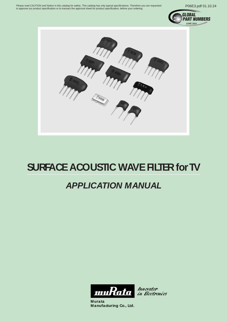
SURFACE ACOUSTIC WAVE FILTER forTV
APPLICATION MANUAL
MurataManufacturing Co., Ltd.
Please read CAUTION and Notice in this catalog for safety. This catalog has only typical specifications. Therefore you are requestedto approve our product specification or to transact the approval sheet for product specification, before your ordering.
P06E3.pdf 01.10.24

IntroductionMurata has continued research on surface acoustic wavefilters since 1970. In 1976 we offered for sale our firstsurface acoustic wave filter to be used in the IF of high-fidelity FM tuners. This product attracted the attentionof the world, because our surface acoustic wave filterwas applied in electronic equipment for consumer usefor the first time in the world. Then, we successfullydeveloped and offered for sale the surface acoustic wavefilter for the video IF of color television sets. Newdevelopments in technology made the television setssmaller in size, which improving their performance yearafter year. With the discrete circuit integrated to IC, theage has come when most of the circuitry of a televisionset, with the exception of the power supply and thetuner, is composed of just 4 LSI and a few transistors.Our surface acoustic wave filter for video IF circuits oftelevision succeeded in making the LC filter block into asolid state device previously left behind integration.Murata has recently developed compact, highperformance resin mold SIP type package for surfaceacoustic wave filters.
Please read CAUTION and Notice in this catalog for safety. This catalog has only typical specifications. Therefore you are requestedto approve our product specification or to transact the approval sheet for product specification, before your ordering.
P06E3.pdf 01.10.24
1 Terms for Surface Acoustic Wave Filters
2 Features
3 Fundamentals
4 Application
5 Appendix
Terms for Surface Acoustic Wave FiltersYYYYY02
Features YYYYYYYYYYYYYYYYYYYYYYYYYYYYYYYYYYYYYYY03
Fundamentals YYYYYYYYYYYYYYYYYYYYYYYYYYYYYYYYY04
3-1. Electrode Pattern Design .........................................................04
3-2. Substrate ...................................................................................05
3-3. Photolithography ......................................................................05
3-4. Sputter .......................................................................................06
3-5. Assembly ...................................................................................06
3-6. Electrical Characteristics .........................................................07
3-6-1. Amplitude characteristics......................................................07
3-6-2. Phase Characteristics...........................................................07
3-6-3. Insertion Loss .......................................................................08
3-6-4. Measurement Circuit ............................................................09
3-6-5. Measurement Method...........................................................10
Application YYYYYYYYYYYYYYYYYYYYYYYYYYYYYYYYYYYY11
4-1. Connection of the Surface Acoustic Wave Filter with Other Blocks ....11
4-1-1. Input/Output Impedances of the Respective Blocks.............11
4-1-2. Connection of the Tuner and the VIF Stage .........................12
4-2. Application Circuit ....................................................................14
4-2-1. Preamplifier System .............................................................14
4-2-2. Postamplifier System............................................................17
4-2-3. Method for the Compensation of the Insertion Loss without Amplifier .......19
Appendix YYYYYYYYYYYYYYYYYYYYYYYYYYYYYYYYYYYYYY20
5-1. Two Detection Methods and the Specification
of the Surface Acoustic Wave Filter ........................................20
5-2. TTE and Direct Breakthrough ..................................................20
5-3. Impedance of the Surface Acoustic Wave Filter ....................22
5-4. Reliability Test ..........................................................................24
5-5. Notice (handling) ......................................................................25
1
2
3
4
5
Please read CAUTION and Notice in this catalog for safety. This catalog has only typical specifications. Therefore you are requestedto approve our product specification or to transact the approval sheet for product specification, before your ordering.
P06E3.pdf 01.10.24
CONTENTS

2
1 Terms for Surface Acoustic Wave Filters
1
¡Surface Acoustic Wave (SAW)An acoustic wave, propagating along a surface of anelastic substrate, whose amplitude decays exponentiallywith substrate depth. ¡Surface Acoustic Wave Filter (SAW Filter)A filter characterized by a surface acoustic wave whichis generated by IDT and propagates along a substratesurface to a receiving IDT. ¡SAW Coupling CoefficientSAW electromechanical coupling coefficient defined byKs2 = 2|∆V/V|, which means the efficiency to transformelectrical energy into acoustic energy or vice versa. ¡IDT (Interdigital Transducer)A comb structure consisting of interleaved metalelectrodes whose function is to transform electricalenergy into acoustic energy or vice versa by means ofthe piezoelectric effect. ¡FingerAn element of the IDT comb electrode.¡Bus BarA common electrode connecting individual fingerstogether.¡Finger OverlapThe length of a finger pair between which onlyelectromechanical interaction is generated.¡ApodizationWeighting produced by the change of finger overlap.¡ApertureMaximum IDT finger overlap length¡TTEUnwanted signals in a SAW filter which has three timestraversed the propagation path between input andoutput IDT's.¡Bulk Wave SignalsUnwanted signals caused by bulk wave excitation,which can be suppressed by grooving the bottom of thesubstrate.¡AbsorberSurface acoustic wave propagates to the right and to theleft because of IDT's symmetrical construction. Siliconrubber is coated on the outer side of IDT's to damp thesurface acoustic wave propagates to outer side.¡Feed Through SignalsUnwanted signals from the input appearing at the filteroutput due to coupling by stray capacitances and otherelectromagnetic couplings.
Fig.1 Dimensions
(in mm)
Input mark
5T1
10m
ax.
14max.
5max
.
Please read CAUTION and Notice in this catalog for safety. This catalog has only typical specifications. Therefore you are requestedto approve our product specification or to transact the approval sheet for product specification, before your ordering.
P06E3.pdf 01.10.24

Please read CAUTION and Notice in this catalog for safety. This catalog has only typical specifications. Therefore you are requestedto approve our product specification or to transact the approval sheet for product specification, before your ordering.
P06E3.pdf 01.10.24
3
2
(1) Provides the same characteristics as conventional LCfilter block with no adjustment.
(2) Labor saving for color television VIF circuit assemblyline.
(3) Make the VIF circuit to be compact and integrated.(4) Extremely beautiful television pictures possible.(5) Temperature coefficient of the trap frequency is
small.(6) Resin molded type available at low prices.(7) Shares very small space on a P.C.B.
2 Features

4
3
3-1. Electrode Pattern Design
The basic configuration of a surface acoustic wave filteris two IDTs on the surface of the piezoelectric substrate.The first IDT connected to the signal source generates asurface acoustic wave, which propagates along asubstrate surface to the second IDT, which transformsSAW energy into electrical voltage on a load connectedto the IDT. Frequency characteristics of the IDTs can becalculated by means of impulse model. In case ofNormal IDT which has a constant pitch and a constantoverlap, the IDT and the corresponding impulse isshown in Fig.2 below. When a voltage is fed to the IDT,the direction of the voltage is the positive-negative-positive-negative direction at λ0/2 interval. The voltageis then subjected to expansion and shrinkage ofsubstrate by the piezoelectric effect. One impulse pair ofadjacent positive and negative polarities is correspondto one electrode pair.When the wavelength of the surface acoustic wavesgenerated by each impulse is equal to the electrodepitch λ0, we get maximum SAW energy.Wave velocity is V, electrode pitch is λ0, number ofelectrode pair is N, then frequency characteristics ofnormal IDT can be calculated by the equations shownbelow.
A(f) =sin NπX
where X = f – f0
, f0 = V
NπX f0 λ0
Frequency characteristics can be changed easily bymeans of weighting. There are two mainly usedweighting method. (a) Varying the Finger Overlap (magnitude of impulse),
called "apodize".(b) Varying pitch (position of impulse), called "variable
pitch."Assuming that impulse of magnitude ai including signsis at the time ti, the summation of waves is given by theequations shown below. This represents the Fouriertransformation itself. Since the impulse is uniquelydetermined when electrode pattern is given, frequencycharacteristics are determined by applying the FourierTransformation. Optimum pattern that correctly meetany specification is designed by means of computersimulation.
NF (f) = ∑ aie–j2πfti
i=1
Fig.2 IDT and the corresponding impulse
Bus bar
Finger
IDT
Impulse
λ0
Fig.3 Frequency characteristics of the normal IDT
0
10
20
f 0
∆ f 2 ∆ f 2 ∆ f 2 ∆ f 2 ∆ f 2 ∆ f 2∆ f
Frequencies (MHz)
Atte
nuat
ion
(dB
)
∆ f f 0
=2N
Fig.4 Weighted impulse
ai
ti
t
3 Fundamentals
Please read CAUTION and Notice in this catalog for safety. This catalog has only typical specifications. Therefore you are requestedto approve our product specification or to transact the approval sheet for product specification, before your ordering.
P06E3.pdf 01.10.24

Please read CAUTION and Notice in this catalog for safety. This catalog has only typical specifications. Therefore you are requestedto approve our product specification or to transact the approval sheet for product specification, before your ordering.
P06E3.pdf 01.10.24
5
3Fundamentals
3
3-2. Substrate
ZnO, and single crystal are usually used as substratematerials for the surface acoustic wave filters.Substrates specifically available for the surface acousticwave filter for color television sets should satisfy thefollowing conditions: (1) The surface acoustic wave electromechanical
coupling coefficient ks is large.(2) The effective dielectric constant is proper.(3) Propagation velocity has a small temperature
coefficient. (4) Propagation loss of the surface wave is small. (5) Stable against heat and little change by aging.(6) Cost of producing the substrate is low.(7) The material constants in/between substrates have
little dispersion.The characteristics (1) through (4) refer to the electricproperties of the surface acoustic wave filter, (5) refer tothe reliability, and (6) and (7) refer to the price of theproduct. The larger the electromechanical couplingcoefficient ks mentioned in (1), the smaller the insertionloss of the surface acoustic wave filter. On the otherhand, the dielectric constant of the substrate is relatedto the impedance of the surface acoustic wave filter. Thetemperature coefficient of the propagation velocitymentioned in (3) determines the temperature coefficientof the center frequency of the filter. Presently, there isno substrate fulfilling all the requirements listed above,and the available materials have both advantages anddisadvantages. Since surface acoustic wave filter forcolor television needs a relatively large substrate size,substrate material cost should be as low as possible.Using well established ZnO sputter techniques, Murataprovides high performance substrates at very low cost.Single crystal substrates are relatively expensivedespite good reproducibility and stability.
3-3. Photolithography
This is a technique for forming fine electrodes on thesubstrate. Process is producing photomasks based onthe designed data, coating resist onto the aluminumevaporated substrate, on which the photomask is setand radiating ultraviolet rays onto the photomask andforming IDT by etching unwanted aluminum. Surfaceacoustic wave filter treating 58MHz of the televisionVIF frequency has more than 100 fine finger electrodes,of which width is about 6 micrometers. Surface acousticwave filters are being manufactured by fully automatedproduction line at strictly environmental controlledroom, for fear of disconnection and shorting by dust.
Table 1 Properties of substrate materials for surface acoustic wave filters
* Non-alkaline glass
LiNbO3
LiTaO3
ZnO/glass*
Substratematerials
128˚Rotated Y
X
–
CrystalCut
X
112˚Y
–
PropagatingDirection
3994
3296
2600
SAWVelocity(m/sec.)
5.6
0.7
1.0
ks2
(%)
–74
–18
–28
TemperatureCoefficient(ppm/°C)
38
51
8.5
DielectricConstant

3
6
3 Fundamentals
3-4. Sputter
For the purpose of getting piezoelectric thin film onglass, ZnO must be deposited on glass substrate bysputtering. A simplified sputtering apparatus is shownin Fig.5. First, berzia is pumped to high vacuum, thenlow pressure argon and oxygen gas flow. Then, a highfrequency voltage is fed to ZnO ceramic target (cathode)so that the argon gas is ionized. Ionized argon goes totarget, makes the target composing element of ZnOsputtered out. These are eventually coated onto the IDTportions of the glass substrate. Murata has establisheda stable technique that can produce high performanceZnO thin film with high deposition rate and lowvariation of C axis orientation.
Fig.5 Sputtering apparatus
Berzia
Glass Plate
ShutterZnO Target
Vaccum Pump
Magnet
RF Voltage Supply
O2+Ar Gas
3-5. Assembly
Lead is soldered directly to the substrate as shown inFig.6 below, thus providing a strong and steadyconnection. This connection has no danger of lead wirebreaking caused by vibration and corrosion caused byhumidity as conventional wire bonding connection.Resin mold and caves on the surface of the substrate areformed by the processes described below. First, wax iscoated on the IDT electrodes of element. Then theelement is coated with resin by dipping. When resin iscured, the wax is melted by heat and is absorbed intothe resin via capillary phenomena, while caves areformed on the surface of the substrate. The first layer ofexternal resin is low expansion coefficient resin used forMurata's FM CERAFIL®. The second layer is moisture-resistant precise resin. (SAFGH Type) Fig.6 Construction of the SAW filter (SAFGH Type)
Resin mold
Lead
ZnO thin film
Absorber
Glass
Please read CAUTION and Notice in this catalog for safety. This catalog has only typical specifications. Therefore you are requestedto approve our product specification or to transact the approval sheet for product specification, before your ordering.
P06E3.pdf 01.10.24

Please read CAUTION and Notice in this catalog for safety. This catalog has only typical specifications. Therefore you are requestedto approve our product specification or to transact the approval sheet for product specification, before your ordering.
P06E3.pdf 01.10.24
7
3
3Fundamentals
3-6-2. Phase CharacteristicsIn the case of surface acoustic wave filters, the outputsignal has a delay with regard to the input signal,corresponding to the time of propagation from input IDTto output IDT of the surface acoustic wave. For example,when a thin film of ZnO sputtered on glass is used aspiezoelectric substrate, the propagation velocity of thesurface acoustic wave is approximately 2600m/sec. Ifthe distance between the input and output IDT is 3mm,the propagation time of the surface acoustic wave willbe approximately 1.2µ sec. Since the delay time of thesurface acoustic wave filter is relatively large as shownabove, the gradient of the phase with regard to thefrequency is large, and as a result, it is hard to observethe phase linearity by measuring its phasecharacteristic. In view of these facts, it is moreconvenient to observe the variations of the group delaytime.SAFGN58M7VH0Z00B03 (shown in Fig.7) is designedby properly compensating for the group delay time viathe chroma bands. Since the short cycle ripple of thegroup delay time critically affect the performance ofthese filters, it is sometimes included in thespecifications of the filter. In this case, ripple is definedas the maximum value of the difference betweenneighbouring peak and valley. The ripple is chieflycaused by the TTE (Triple Transit Echo) in most cases,but it may also be caused by the direct breakthrough.
3-6. Electrical Characteristics
Fig.7 Frequency characteristics of SAFGN58M7VH0Z00B03
Frequency (MHz)
Gro
up D
elay
Tim
e (n
sec.
)
Atte
nuat
ion
(dB
)
0
10
20
30
40
50
60
70
1800
1600
1400
1200
1000
800
600
400
52 54 56 58 60 62
3-6-1. Amplitude characteristicsFig.7 shows the characteristics of the surface acousticwave filter for the television VIF circuit. Beingremarkably different from conventional LC filters, theSAW filter has a response of many peaks and bottomsoutside the pass band. It is necessary to add the items ofspurious attenuation of upper side and lower side.

8
3
3 Fundamentals
3-6-3. Insertion LossAs terms to express loss there are insertion loss andpower loss. In some cases there is confusion regardingthese two terms, but here we introduce one term more,i.e., voltage loss, and make a clear distinction betweenthe definitions of each term as follows; In Fig.8 (a) VS isthe signal source voltage, VL is the output voltage, RS isthe signal source impedance, and RL is the loadimpedance. The insertion loss is defined as the ratio ofthe output voltage VLS when filter is removed and shortcircuited by jumper wire, as shown in Fig.8 (b), to themaximum output voltage when filter is inserted. In thiscase, attention should be paid to the fact that theinsertion loss is not the ratio of the signal source voltageVS to the output voltage VL. Even when the ratio of VS
to VL is constant, the insertion loss can be changedwhen the ratio of RS to RL is changed. In this brochurethe ratio of the signal source voltage VS to the outputvoltage VL, i.e., 20 log (VS/VL) is defined as voltage loss.From the considerations presented above, the followingrelation can be obtained:
Insertion loss = Voltage loss – 20 logRS + RL
....... (1)RL
Power loss is defined as the ratio of the available powerof the signal source and the power supplied of the loadas follows:
Power loss = 10 log (VS2/4RS) / (VL2/RL)= 20 log (VS/VL) + 10 log (RL/4RS)
Thus,
Power loss = Voltage loss + 10 log (RL/4RS) .................. (2)
From (1) and (2) we obtain the following relation:
Power loss = Insertion loss + 10 log (RS + RL)2 / 4RSRL
.................. (3)From (3) it is possible to see that when RS = RL, wehave:
Power loss = Insertion lossThe following considerations are developed based uponthe definitions above. The power loss of a SAW filter isdetermined by the relation of the impedance of the filteritself and the terminating impedances at imput andoutput sides. Close to the center frequency of the SAWfilter, the input and output impedances of the filteritself is expressed as a capacitance and a resistance inparallel. This resistance is called radiation resistance,and the power consumed by this resistance becomes thesurface wave energy. Thus, the power loss can bereduced by performing an effective consumption ofpower by this radiation resistance. When the signalsource impedance RS and the load impedance RL are
Fig.8 Effect of power dissipation by incorrect insertion of SAW filter
(a)
(b)
V
V
RS
VS RL VL
RS
VS RL VLS
RL
RS + RLVLS = VS
Please read CAUTION and Notice in this catalog for safety. This catalog has only typical specifications. Therefore you are requestedto approve our product specification or to transact the approval sheet for product specification, before your ordering.
P06E3.pdf 01.10.24

Please read CAUTION and Notice in this catalog for safety. This catalog has only typical specifications. Therefore you are requestedto approve our product specification or to transact the approval sheet for product specification, before your ordering.
P06E3.pdf 01.10.24
9
purely resistive, assuming RS is equal to the absolutevalue of the input impedance Zin of the SAW filter, andRL is equal to the absolute value of the outputimpedance Zout of the SAW filter, the power lossbecomes minimum.(*)
(*) Strictly speaking, the condition for minimum powerloss slightly differs from the condition RS = | Zin |,RL = | Zout |
Since Zin and Zout have capacitive components, thepower loss can be further decreased by performing thecancellation of these capacitive components by means ofinductance, and matching the remaining pure resistivecomponents with RS and RL. In this case the power lossis actually minimized thanks to the conjugateimpedance matching. As described above, the power losscan be reduced by means of the impedance matching ofthe input/output impedances of the SAW filter, but it isknown that the level of the TTE (Triple Transit Echo)and the power loss are in conflicting relation, i.e., whenthe power loss is reduced the TTE increases. A requiredsuppression of the TTE in cases of practical use is–40dB, and in order to attain that value, it is saidtheoretically that the power loss of the SAW filtershould be larger than 16dB. Thus, in cases of practicalapplication, instead of matching perfectly, the SAWfilter is mismatched to some extent, with a power losslarger than 16dB (in order to make possible a certainmargin of safety, the actual value of the power lossshould be larger than 18dB).
3
3Fundamentals
Fig.9 Measuring Circuit
75 15pF
SAFGN58M7VH0Z00B03
255
560 10
0
75
1 2 3 4
TA7124P
5 6 7
V
+B
1.1µ
H
0.75
µH
3-6-4. Measurement CircuitFig.9 shows measuring circuit ofSAFGN58M7VH0Z00B03. To reduce the power loss,parallel tuning coil is used. Since the insertion loss ofSAW filters is large, output signal becomes low. Andfeed through signals make the accurate measurementdifficult, requiring attention to the shielding of the testfixture.

Please read CAUTION and Notice in this catalog for safety. This catalog has only typical specifications. Therefore you are requestedto approve our product specification or to transact the approval sheet for product specification, before your ordering.
P06E3.pdf 01.10.24
10
3
3 Fundamentals
Fig.10 Block Diagram of Pulse Response Measurement System
RFGenerator
HP 10514A
Mixer
Annstu MG411B
Pulse Generator
Amp.1 Amp.2
Amp.3
ch2ch1
Amp.1 Amp.2 Amp.3 : HP 8447A(20dB Gain)
National VP-5520A
Oscilloscope
AttenuatorR1 R2
Zin=Zout=50 0hm Zin=Zout=50 0hm
Picture CarrierFrequency
∆T ∆T
∆T=200 nsec.
∆T
Fig11 Typical Pulse Response Waveform
Input
ch1
Main Signal
VM
Edge Reflection, Bulk Wave
TTEVT
Time
Time
ch2
DirectBreakthrough
TTE=20log VT
VM
2
3-6-5. Measurement Method¡Measurement by means of network analyzerAmplitude and phase, group delay time characteristicscan be measured directly by means of the RF networkanalyzer. Network analyzer for this use is made byseveral makers. Surface acoustic wave filter for video IFof television sets has many specified points. Murataadopted the synthesizer type programmable networkanalyzer, which measures quickly and accurately,judges of go or no go for the specifications automatically.¡Measurements in the time domain The measurement system used to verify the spuriouslevels of the TTE, etc., is shown in Fig.10. Typical pulseresponses are shown in Fig.11. Pulse rise time should beoptimally long, because "ears" may appear in theresponse waveforms due to the band limitations of thefilter which disturbs measuring.
Please read CAUTION and Notice in this catalog for safety. This catalog has only typical specifications. Therefore you are requestedto approve our product specification or to transact the approval sheet for product specification, before your ordering.
P06E3.pdf 01.10.24
11
4
4 Application
4-1. Connection of the Surface Acoustic W ave Filter with Other Blocks
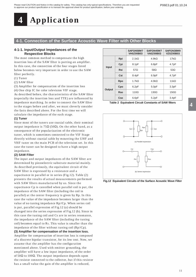
Table 2 Equivalent Circuit Constants of SAW filters
Fig.12 Equivalent Circuits of the Surface Acoustic Wave Filter
Cpi CpoRpi
Rpo
(a) Parallel expression
Csi Cso
Rsi Rso
(b) Series expression
4-1-1. Input/Output Impedances of theRespective Blocks
The most common method to compensate the highinsertion loss of the SAW filter is putting an amplifier.In this case, the connection of the four stages listedbelow becomes very important in order to use the SAWfilter perfectly. (1) Tuner(2) SAW filter(3) Amplifier for compensation of the insertion loss(4) One chip IC for color television VIF stage. As described before, the characteristics of the SAW filter(especially the insertion loss and TTE) are influenced byimpedance matching. In order to connect the SAW filterto the stages before and after, we must cleverly considerthe facts described above. For the first time we willcalculate the impedance of the each stage.(1) TunerSince most of the tuners use coaxial cable, their nominaloutput impedance is 75Ω (50Ω). On the other hand, as aconsequence of the popularization of the electronictuner, which is sometimes connected to the VIF Stagedirectly without coaxial cable by mounting the UHF andVHF tuner on the main PCB of the television set. In thiscase the tuner can be designed to have a high outputimpedance. (2) SAW FilterThe input and output impedances of the SAW filter aredetermined by piezoelectric substrate material mainly.As described previously, the equivalent circuit of theSAW filter is expressed by a resistance and acapacitance in parallel or in series (Fig.12). Table (2)presents the results of actual measurements performedwith SAW filters manufactured by us. Since thecapacitance Cp is cancelled when parallel coil is put, theimpedance of the SAW filter (including the coil inparallel) at the center frequency is given by Rp. In thiscase the value of the impedance becomes larger than thevalue of no tuning impedance Rp//Cp. When series coilis put, parallel expression of Fig.12 (a) should bechanged into the series expression of Fig.12 (b). Since inthis case the tuning coil and Cs are in series resonance,the impedance of the SAW filter (including the tuningcoil) becomes equal to RS. This value is smaller than theimpedance of the filter without tuning coil (Rp//Cp).(3) Amplifier for compensation of the insertion loss.Amplifier for compensation of insertion loss is composedof a discrete bipolar transistor, for its low cost. Now, weassume that the amplifier has the configurationmentioned above. Used with emitter grounding, theamplifier will have a low input impedance, of the orderof 50Ω to 100Ω. The output impedance depends uponthe resistor connected to the collector, but if this resistorhas a small value the gain of the amplifier is reduced,
Input
Output
Rpi
Cpi
Rsi
Csi
Rpo
Cpo
Rso
Cso
17kΩ
4.7pF
53Ω
4.7pF
11kΩ
3.3pF
150Ω
3.4pF
SAFGN38M9VZ0Z00B03
4.9kΩ
6.8pF
58Ω
6.9pF
4.0kΩ
5.0pF
130Ω
5.2pF
SAFGN45M7VA0Z00B03
2.1kΩ
8.1pF
57Ω
8.4pF
1.7kΩ
6.2pF
110Ω
6.6pF
SAFGN58M7VH0Z00B03

Please read CAUTION and Notice in this catalog for safety. This catalog has only typical specifications. Therefore you are requestedto approve our product specification or to transact the approval sheet for product specification, before your ordering.
P06E3.pdf 01.10.24
12
4
4 Application
and if it is a large value, the output impedance of thetransistor itself will be upper limit. Thus, it is of theorder of 100Ω to 1 kΩ is useful. (4) One chip IC for VIFThe input impedance of the one chip IC for televisionVIF is of the order of 1kΩ to 3kΩ.
4-1-2. Connection of the T uner and the VIF StageWhen using the SAW filter, the importance of itsrelation with the impedances of the stages located afterand before the SAW filter was already described. Inaddition, the connection between the tuner and the nextstages requires special attention. As shown in Fig.13,there are many types of IF output circuits of the tuner.The most commonly used circuit is that shown in (a),but the double tuning system of (b) and (c), and thecascade circuit of (d) and (e) are also used. The IFoutput frequency characteristics of the tuner dependupon the circuit used. The overall frequencycharacteristic of the television set is determined by thecombination of the frequency characteristic of the tunerIF output stage and the frequency characteristic of theSAW filter. Thus, even when the overall characteristicof the VIF stage of the television set is known, therequired frequency characteristic of the SAW filter canbe changed if the IF characteristic of the tuner, usedtogether with the SAW filter, is changed. In otherwords, if there is a SAW filter with a givencharacteristic, it is necessary to connect with a tunerpresenting characteristics conveniently matched withthe SAW filter. For example, to combine a VIF stage toa tuner with single tuning IF output circuit, in somecases, it is required to make a resonant circuit betweenthe IF output circuit of the tuner and input circuit of theVIF stage, as shown in Fig.14, virtually performing adouble tuning circuit. In this case, if the LC of the VIFstage is removed and replaced by a SAW filter, thecircuit will be a single tuning one, and as a result theoverall bandwidth may become narrower. When theoverall bandwidth is narrow, the most simple solution isthe use of the resistor in parallel with the input of theVIF stage to damp the Q of the circuit to widen the IFoutput bandwidth. However, this action makes thevoltage level to be reduced, it is recommended to changethe tuner with another one to have a wider bandwidth.In order to increase the bandwidth of the IF outputstage, one must adopt the double tuning as shown inFig.13 (b), (c) or damp the Q of the circuit by means ofdamping resistor, as shown in (d) and (e) a cascadecircuit is used for fear of gain reduction due to the Q-damping and also to improve the stability of the circuit.On the other hand, in circuits like that shown in (a), itis possible to widen the bandwidth by changing thecircuit constant, as shown in (a'). The nominal outputimpedance of the tuner is 75Ω, but in actual cases itoften has strong frequency dependence as shown in
Fig.13 Various Types of IF Output Circuit of the Tuner
22
22
IF
10
OUT
+B
(b)
1000
1000
OSC
68
56
(a)
OSC 2
56
15
1000
47
1000+B
39
IF OUT
(a')
OSC 2
10
1000
2200
1000+B
22
IF OUT
OSC
1000
1000
IF OUT
+B
(C)
IF OUT
+B
4
OSCOSC
IF OUT20
39
1000
(d) (e)
+B
1000 10001000
10
1000
Fig.14
TunerCoaxial Cable
VIF Stage
Trap

Please read CAUTION and Notice in this catalog for safety. This catalog has only typical specifications. Therefore you are requestedto approve our product specification or to transact the approval sheet for product specification, before your ordering.
P06E3.pdf 01.10.24
13
4Application
4
Fig.15. Figure 15 (a) corresponds to the Fig.13 (a) withthe popular π type circuit, and Fig.15 (b) corresponds tothe Fig.13 (b) with the double tuning circuit. Fig.15 (c)corresponds to the case of Fig.13 (a'), and in this circuitthe output impedance has a very weak frequencydependence. Connecting the tuner output to the SAWfilter directly (for example, the case of the post amplifiersystem described later), the strong frequencydependence of the tuner output impedance may bedifficult problem. Reactance of tuner output changingfrequency to frequency will change the tuning state ofSAW filter to make the shape of amplitudecharacteristics of the SAW filter change from its ownone. Thus, in the post-amplifier system it is desirable touse a tuner with nearly constant output impedance, asshown in Fig.15 (c). On the other hand, in thepreamplifier system described later, output impedancechanging of the tuner is not so difficult problem, beingsufficient to consider only the bandwidth of the IFoutput stage. In other words, since the preamplifierplays the role of a buffer, the SAW filter connected afterit is not influenced by the tuner output impedance.
Fig.15 (b) IF Output Impedance of the Tuner
1
20.5
0.2
- j x / Z0
1
2
0.2
0.5
+j x
/ Z0
0 0.2 0.5 1 2
Z0=75Ω
R/Z0
fpfc fs
Fig.15 (a) IF Output Impedance of the Tuner
Z0=75Ω1
2
1
2
0.5
0.2
0.5fs
0.2
0 0.2
fp R/Z0
0.5 1
- j x / Z0
+j x
/ Z0
2
fc
Fig.15 (c) IF Output Impedance of the Tuner
1
20.5
0.2
- j x / Z0
1
2
0.2
0.5
+j x
/ Z0
0 0.2 0.5 1
Z0=75Ω
fpfc
R/Z0
fs
2

Please read CAUTION and Notice in this catalog for safety. This catalog has only typical specifications. Therefore you are requestedto approve our product specification or to transact the approval sheet for product specification, before your ordering.
P06E3.pdf 01.10.24
14
4 Application
4-2. Application Circuit
Fig.16 Preamplifier System
Tuner
VIF1 chip IC
R2
R1
RLRS
(a)
V
(b)
Fig.17 Relation between the Terminating Impedance and the Ripple of the Group Delay Time Characteristic (Parallel tuning)
Rs=150Ω
Rs=220Ω
Rs=560Ω
Rs=1kΩ
Gro
up D
elay
Tim
e
100n
sec.
55 56 57 58 59
Rs 15pF
1.1µ
H
0.75
µH
560 V
Fig.18 Relation between the Terminating Impedance and the Ripple of the Group Delay Time Characteristic (Series Tuning)
Rs=1kΩ
Rs=220Ω
Rs=75Ω
Rs=25Ω
Gro
up D
elay
Tim
e
100n
sec.
55 56 57 58 59
Rs
0.68µH
75 V
4-2-1. Preamplifier System¡Preamplifier systemThe system where the insertion loss compensationamplifier is placed before the SAW filter is called apreamplifier system. Fig.16 (a) is an example of apreamplifier system, and it can be converted into theconfiguration shown in Fig.16 (b) in AC operation. Thevalue of RS shown in Fig.16 (b) can be controlled bychanging the value of R1. On the other hand, RL can alsobe controlled by changing the value of R2. As describedpreviously, the insertion loss of the SAW filter dependsupon the impedance matching. To make the externalterminating impedance equal to the impedance of theSAW filter (impedance of the SAW filter including thetuning coil, when such a coil is used), gets minimuminsertion loss. But SAW filter should be mismatched inorder to suppress the TTE. When in no tuning and inparallel tuning, making the terminating impedance tobe mismatched to the lower side makes TTE reduced (sothat the ripple on the group delay time characteristic isreduced as shown in Fig.17). On the contrary, themismatching to the higher side makes TTE increase.Too small RS and RL bring high power loss, the values ofRS and RL must be determined with making compromisebetween the TTE suppression and the voltage gain. Inthe case of series coil tuning the situation is inverse. Asshown in Fig.18, when the external terminatingimpedance is mismatched to the higher side, the TTEreduces.
4

Please read CAUTION and Notice in this catalog for safety. This catalog has only typical specifications. Therefore you are requestedto approve our product specification or to transact the approval sheet for product specification, before your ordering.
P06E3.pdf 01.10.24
15
4Application
4
¡Considerations referring to the gain in thepreamplifier system.
In Fig.20, since capacitance of the SAW filter, transistorand VIF IC can be cancelled by means of the coilconnected in parallel, only the resistive component maybe taken into consideration. The simplified equivalentcircuit of Fig.19 will have the final configuration shownin Fig.20. The circuit shown in Fig.20, is consideredequivalent to the actual working state of Fig.19. Thelast circuit is used as test circuit. In Fig.20 the voltagegain G between the input and the output is expressedas:
G = 20 log (e0/ei) .................................................................................... (1)Assuming insertion loss of SAW filter is L (dB) (L>0),and output voltage when L = 0 is E0 (equivalent to thesituation with the filter removed and short circuited bythe jumper wires), the following relation is valid:
E0 = ei·gm·RS·RL / (RS + RL) ......................................................... (2)Thus, from the definition of the insertion loss in 3-6 wehave:
G = 20 log (e0/ei) = 20log (E0/ei) – L= 20 log (gm·RS·RL / (RS + RL)) – L ....................................(3)
Assuming the power loss of the SAW filter is K(dB), theequations 3-6-3, (3) give the following equation.
G = 20 log (gm·RS) + 10 log (RL/4RS) – K ........................... (4)In order to increase the value of G, the values of 20 log(gm·RS) and 10 log (RL/4RS) should increase and thevalue of K should be reduced. However, K should bemore than 16 or 18 dB in order to suppress the TTE. 20log (gm·RS) is the voltage gain of the preamplifier, gmdepends upon collector current of the transistor. Whenthe source voltage is given, the maximum output level isdetermined as a consequence of linearity of theamplifier, and thus, in actual cases the voltage gain ofthe preamplifier can be considered constant.Consequently, only 10 log (RL/4RS) remainsundetermined. RL/RS should be as large as possible, (apower loss of the order of 16 - 18 dB). For example, if thepower loss K of the SAW filter is assumed as 16dB(constant), the total voltage gain and RL/RS will presentthe relation shown in Fig.21. Fig.21 shows that whenthe gain of the preamplifier is constant, the total gainincreases with the ratio RL/RS.
¡Cautions for preamplifier systemSince the signals of the preamplifier are amplified tohigh levels, it is necessary to prevent distortions due tothe intermodulation. To insert resistance of negativefeed back on emitter is commonly used. Thepreamplifier system is suited for high impedance SAWfilters. Using a low impedance SAW filter with thepreamplifier system, the values of RS and RL shown inFig.20 will be very low for fear of TTE, and as a resultthe gain of the preamplifier, 20 log (gm·RS) is reduced.In the preceeding chapter, RS change could be
Fig.21 Relation between the Total Voltage Gain and RL/RS
Fig.19
15
10
5
Tot
al V
plta
ge G
ain
(dB
)
0
-5
-100 1 2 3 4 5
RL/Rs
Power Loss of the SAW Filter=16dB(constant)
20log(gmRs)=26dB
23dB
20dB
17dB
VIF ICSAWFilter R2e0Q
ei
R1
+B
Fig.20
SAWFilter
R2 Rin
Where Rc : Output resistance of Q Rin : Input resistance of VIF IC
e0
R1Rc
V
SAWFilter RL
Where Rs=Rc//R1
RL=Rin//R2
e0V
Rs
eigmRs
eigm

Please read CAUTION and Notice in this catalog for safety. This catalog has only typical specifications. Therefore you are requestedto approve our product specification or to transact the approval sheet for product specification, before your ordering.
P06E3.pdf 01.10.24
16
4
4 Application
compensated for by changing gm as a result of changingthe collector current, resulting therefore in a constantvalue of 20 log (gm·RS). However, when the value of RS
is too small, the collector current is limited by itsmaximum collector dissipation, gm are not become sohigh. Consequently it is not possible to compensate thereduction of RS. In using low impedance SAW filters inthe preamplifier system, the following modifications arerequired.
¡Use of the low impedance SAW filter in the preamplifier system.
An impedance conversion circuit is required for the useof a low impedance SAW filter in the preamplifiersystem. Fig.22 shows an example of use of a lowimpedance SAW filter in the preamplifier system. Awell-known impedance conversion circuit usingtransformer tap down shown in Fig.23 (a) can bemodified to the circuit shown in Fig.23 (b) , withcapacitance tap down, the capacitance of the SAW filterin Fig.22 corresponds to the capacitance C2 of Fig.23 (b).The coil plays a part of transformer as well as a tuningcoil. In Fig.23 (b) the equivalent transformation ratio isgiven by C1 : (C1 + C2), and the impedance ratio is givenby C12 : (C1 + C2)2. Thus, an arbitrary impedancetransformation can be attained by selecting aconvenient value of C1. In the circuit in Fig.22, theimpedance at the input side of the SAW filter can bereduced by stepping-down, and at the output side theimpedance can be increased by stepping-up. Thus, inthis case it is possible to use a low impedance SAWfilter with the same peripheral circuit used in the caseof a high impedance SAW filter. Fig.23 Transformation Circuits
Transformation Ratio n1:n2
(a)
n1
n2
Transformation Ratio(C1+C2):C1
C1
C2
(b)
Fig.22 A Circuit Using a Low-impedance SAW Filter in the Preamplifier System
Tuner
VIF 1 chip IC
C1
C'1
C'1
+B

¡Considerations about the relation between thepower loss of a SAW filter and the noise figure ofthe postamplifier system
In the postamplifier system, for reason of the low signallevel after the SAW filter, they suspect a deteriorationin the noise figure. The noise figure of the block diagramshown in Fig.25 should be discussed. Here, in order tosimplify the discussion, the SAW filter is assumed as anattenuator with gain Gf . Assuming that only thermalnoise is generated, and that both the tuner and theSAW filter have the same bandwidth B, the noise figureFf of the SAW filter will be expressed as follows:
Where kB is Boltzman's constant, T is the absolutetemperature of the filter, B is the bandwidth and Noutis the output noise level. The noise figure of this systemwill be given by:
Fig.26 shows the relation between the power loss of theSAW filter and the noise figure of the total system, with
F = Ft +Ff – 1
+Fa – 1
+Fν – 1
Gt Gt·Gf Gt·Gf ·Ga
Please read CAUTION and Notice in this catalog for safety. This catalog has only typical specifications. Therefore you are requestedto approve our product specification or to transact the approval sheet for product specification, before your ordering.
P06E3.pdf 01.10.24
17
4Application
4
Fig.24
Tuner
+B
VIF1chip IC
Fig.25
Tuner
Noise Figure FtGain Gt
FfGf
FaGa
Fv
SAWFilter
Sin Sout PostAmplifier
VIF IC
4-2-2. Postamplifier System¡Postamplifier systemThe system using the amplifier for compensation of theinsertion loss after the SAW filter is called postamplifiersystem. Fig.24 shows an example of postamplifiersystem. If the postamplifier is composed of an emittergrounded bipolar transistor, the input impedance willhave a value of the order of 50 to 100Ω. Usually theoutput impedance of the tuner has a nominal value of75Ω. The external terminating impedances of thepostamplifier system can not be changed so easily as thepreamplifier system. When both input and output ofthe high impedance SAW filter are terminated by 75Ω,the mismatching rate is too much, resulting in largeinsertion loss, it is necessary to modify the circuit asdescribed below section. When low impedance SAWfilter is terminated by 75Ω, both the TTE suppressionand the insertion loss can be arranged at a suitablevalue. However, since the input impedance of the SAWfilter seen from the tuner is not perfectly 75Ω, thefrequency characteristic of the IF output stage of tuneris sometimes influenced by SAW filter impedance. Forexample, if the input impedance of the SAW filter islarger than 75Ω, the Q factor of the IF output circuit ofthe tuner becomes high, and as a result the bandwidthmay become narrower. To prevent this, it is necessary toinsert a Q damping resistor in parallel with the inputterminals of the SAW filter.
Fig.26
Power Loss of SAW Filter (dB)
Tuner
GfFf
Fa=20dBGa=3dB
SAWFilter
PostAmplifier VIF IC
Fv=8dB
Constant
2
0
2
4
6
8
10
12
14
4 8 10 12 14 16 18 20 22 246
Noi
se F
igur
e of
Sys
tem
F(d
B)
Ft=3dB
Ft=5dB
Ft=7dB
40
40
35
3025
35
25
Gt=40dBGt=35dBGt=30dBGt=25dB
Ff = (Sin/kBTB)/(Sout/Nout) = (Sin/kBTB)/Gf ·Sin 1( ) = 1 +
(1+Gf )kBTB Gf

Please read CAUTION and Notice in this catalog for safety. This catalog has only typical specifications. Therefore you are requestedto approve our product specification or to transact the approval sheet for product specification, before your ordering.
P06E3.pdf 01.10.24
18
4
4 Application
the tuner gain Gt and the tuner noise figure Ft taken asparameters. According to Fig.26 on the condition thatthe tuner gain is larger than 30dB, the deterioration ofthe noise figure of the total system does not exceed 1dBeven when the power loss of the SAW filter is 24dB.Thus, when using a SAW filter in the postamplifiersystem it is desirable to connect a high gain tuner, andin order to prevent the deterioration of the SN ratio athigh input level, it is desirable to use a tuner which hashigher signal level at which AGC begins to operate. (i.e.,Handling signal level of mixer transistor (or FET) of thetuner is high). Fig.27 shows calculation results of thenoise figure of total system assuming postamplifiernoise figure is 2dB, 3dB and 4dB. These results showthat the noise figure of postamplifier has less effectiveupon the noise figure of total system than the gain andnoise figure of the tuner, Fig.28 presents the calculationresults of the noise figure of the total system assumingthat VIF ICs noise figure is 6dB, 8dB and 10dB. The 3curves are almost superimposed. As a result, thedeterioration of the SN ratio due to the insertion loss ofthe SAW filter can be avoided by using the convenienttuner.
Fig.27
Power Loss of SAW Filter (dB)
Tuner
Gf=33dBFf= 4dB
Ga=20dBFa
SAWFilter
PostAmplifier VIF IC
Fv=8dB
2
0
2
4
6
8
10
12
14
4 8 10 12 14 16 18 20 22 246
Noi
se F
igur
e of
Sys
tem
F(d
B)
Fa=2dBFa=3dBFa=4dB
Fig.28
Power Loss of SAW Filter (dB)
Tuner
Gf=33dBFf= 4dB
Ga=20dBFa= 3dB
SAWFilter
PostAmplifier VIF IC
Fv
2
0
2
4
6
8
10
12
14
4 8 10 12 14 16 18 20 22 246
Noi
se F
igur
e of
Sys
tem
F(d
B)
Fv=6,8,10dB 3 Curves Superposed
Fig.29 Use of a High Impedance Type SAW Filter in the Postamplifier System
Tuner VIF 1 chip IC
+B
¡Use of a high impedance SAW filter in the postamplifier system.
We have said that the low impedance SAW filter isbetter to use for postamplifier system because theterminating impedance of SAW filter is limited to low,high impedance SAW filters can also be usable bymeans of series coil tuning, as described below. TheSAW filter impedance can be expressed by means of theparallel expression and the series expression, as shownin Fig.12, which can be converted mutually. For seriescoil tuning, it is easier to analyze with the equivalentcircuit with the series expression. Tuned with seriescoil, the apparent impedance of the SAW filter becomesRsi (Rso). Table (2) shows the Rsi (Rso) of the seriesexpression is very small compared with Rpi (Rpo) of theparallel expression. The impedances of high impedancetype SAW filter SAFGN58M7VH0Z00B03,SAFGN45VA0Z00B03 become very low of the order of50Ω. Thus, even the high impedance SAW filters can beused in the postamplifier system by means of the seriescoil tuning. Fig.29 shows an example of a circuit using ahigh impedance type SAW filter in the postamplifiersystem. Since the output side of the SAW filter isconnected to the postamplifier, of which inputimpedance is of the order of 50 to 100Ω, which brings aheavy mismatching. The input side of the SAW filter isclose to the matching thanks to the series tuning coil, asa whole total power loss becomes high to suppress theTTE.
Please read CAUTION and Notice in this catalog for safety. This catalog has only typical specifications. Therefore you are requestedto approve our product specification or to transact the approval sheet for product specification, before your ordering.
P06E3.pdf 01.10.24
19
4Application
4
Fig.31
(a) High impedance type
TunerHigh Gain
VIF 1 chip ICSAWFilter
(b) Low impedance type
TunerHigh Gain
VIF 1 chip ICSAWFilter
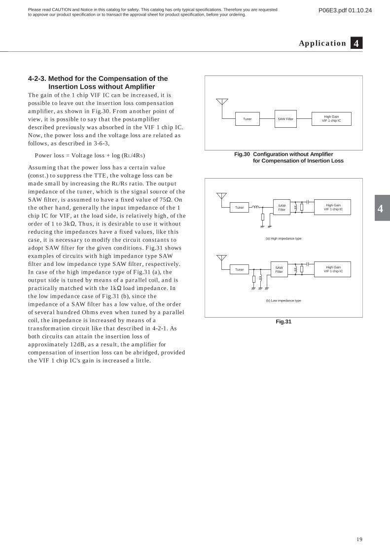
4-2-3. Method for the Compensation of theInsertion Loss without Amplifier
The gain of the 1 chip VIF IC can be increased, it ispossible to leave out the insertion loss compensationamplifier, as shown in Fig.30. From another point ofview, it is possible to say that the postamplifierdescribed previously was absorbed in the VIF 1 chip IC.Now, the power loss and the voltage loss are related asfollows, as described in 3-6-3,
Power loss = Voltage loss + log (RL/4RS)
Assuming that the power loss has a certain value(const.) to suppress the TTE, the voltage loss can bemade small by increasing the RL/RS ratio. The outputimpedance of the tuner, which is the signal source of theSAW filter, is assumed to have a fixed value of 75Ω. Onthe other hand, generally the input impedance of the 1chip IC for VIF, at the load side, is relatively high, of theorder of 1 to 3kΩ, Thus, it is desirable to use it withoutreducing the impedances have a fixed values, like thiscase, it is necessary to modify the circuit constants toadopt SAW filter for the given conditions. Fig.31 showsexamples of circuits with high impedance type SAWfilter and low impedance type SAW filter, respectively.In case of the high impedance type of Fig.31 (a), theoutput side is tuned by means of a parallel coil, and ispractically matched with the 1kΩ load impedance. Inthe low impedance case of Fig.31 (b), since theimpedance of a SAW filter has a low value, of the orderof several hundred Ohms even when tuned by a parallelcoil, the impedance is increased by means of atransformation circuit like that described in 4-2-1. Asboth circuits can attain the insertion loss ofapproximately 12dB, as a result, the amplifier forcompensation of insertion loss can be abridged, providedthe VIF 1 chip IC's gain is increased a little.
Fig.30 Configuration without Amplifier for Compensation of Insertion Loss
TunerHigh Gain
VIF 1 chip ICSAW Filter

Please read CAUTION and Notice in this catalog for safety. This catalog has only typical specifications. Therefore you are requestedto approve our product specification or to transact the approval sheet for product specification, before your ordering.
P06E3.pdf 01.10.24
20
5
5 Appendix
5-1. Two Detection Methods and the Specification of the Surface Acoustic W ave Filter
Fig.32 Two Detection Methods
VIF IC Detector stage
VIF IC Detector stage
Sound Carrer Trap
Synchronous Detector
SynchronousDetector
SynchronousDetector
Amplifier
Input Video Output
Sound IF Output
Input
CarrierLimit
(a)
Video Output
Sound IF Output
CarrierLimit
(b)
There are two detection methods for the 1 chip IC of theVIF, which are shown in Fig.32 (a) and (b). Bothmethods adopt the LLD (Low Level Detector), of asynchronous detection method. In (a) the intercarriertype sound IF detection and video detection areperformed by the same detector, but in (b) they areseparated. In (b) the signal is divided in two, one issupplied to the sound IF detector and another issupplied to the video detector through the sound carriertrap. In (a) there is the problem of the 920kHz beat(ƒc–ƒs). we can not increase excessively the level of thesound carrier, so that sound carrier attenuation of theSAW filter should be required of the order of 18dB to24dB from the peak. On the other hand, in the method(b), since a sound carrier trap is inserted before thevideo detector, there is no problem of 920kHz beat. Inthis case, in order to increase the output of the soundIF, sound carrier attenuation of the SAW filter shouldbe required to have the order of l0dB to 18dB from thepeak. As a result there are two required frequencycharacteristics of SAW filter (especially the attenuationat the sound carrier frequency) depending upon the typeof IC used (detection method used).
5-2. TTE and Direct Breakthrough
Suppose the TTE and the direct breakthrough are notsufficiently suppressed, there will be a superposition ofsignals with time delay (or advance) upon the mainsignal, producing as a result ghost troubles upon thepicture of the television set. For the TTE, since its delayis 2τ sec. with regard to the main signal, the ghost willappear at the right side, and for the directbreakthrough, the ghost will appear at the left side dueto its τ sec. advance(*). Whether TTE and directbreakthrough are suppressed sufficiently can beobserved by the amplitude characteristics and the groupdelay time characteristics of the VIF stage. In otherwords, as TTE or direct breakthrough interferenceswith the main signal, to result in periodic ripples in theamplitude characteristics and group delay timecharacteristics, the suppression of the TTE and directbreakthrough can be inferred from magnitude of theripples. The ripple period ∆ƒ is 1/2τ Hz when caused bythe TTE, and 1/τHz when caused by the directbreakthrough. Thus, we can imagine roots of ripple byseeing the period of ripples. For example, in case ofSAFGN58M7VH0Z00B03 τ is approximately 1.0µsec.,and thus the period of the ripples due to TTE is
(*) See Fig.12

Please read CAUTION and Notice in this catalog for safety. This catalog has only typical specifications. Therefore you are requestedto approve our product specification or to transact the approval sheet for product specification, before your ordering.
P06E3.pdf 01.10.24
21
5
5Appendix
Fig.33
0
10
20
30
40
50
60
70
1800
1600
1400
1200
1000
800
600
400
47.0 52.0 57.0
(a) Frequency characteristics when the directbreakthrough is sufficiently suppressed
Frequency (MHz)
62.0 67.0
Atte
nuat
ion
(dB
)
Gro
up d
elay
tim
e (n
sec.
)
0
10
20
30
40
50
60
70
1800
1600
1400
1200
1000
800
600
400
47.0 52.0 57.0
(b) Frequency characteristics when the directbreakthrough is not suppressed
Frequency (MHz)
62.0 67.0
Atte
nuat
ion
(dB
)
Gro
up d
elay
tim
e (n
sec.
)
Fig.34
fc fp
12τ
Frequency
(a)
Det
ecto
r O
utpu
t (D
C)
1τ
Frequency
(b)
Det
ecto
r O
utpu
t (D
C)
fc fp
approximately 500kHz. High level of directbreakthrough makes not only the ripples in the groupdelay time and amplitude but also the trap depthsreduction as shown in Fig.33, with deterioration in theattenuation level outside the pass band. As describedpreviously TTE level can be suppressed to less than–40dB by increasing the power loss to a value largerthan 18dB, by means of the mismatching. On the otherhand, the level of the direct breakthrough is influencedby the printed circuit layout. The causes of the directbreakthrough can be classified in 3 items:
– Electrostatic causes like stray capacitance, etc. – Electromagnetic inductions due to the currents
passing through the printed pattern– Due to the residual resistance of the common ground.
With regard to the electrostatic causes, the printedInput/Output patterns should be made sufficientlysmall and short, VIF stage including VIF IC, SAW filteretc. should be shielded from other stage, In many cases,the design of the earth pattern has an importantinfluence upon the direct breakthrough level. Inconventional LC filters, every free space on the printedcircuit board is filled as much as possible with earthpattern, which is mutually connected wherever possible.However, this configuration is not suited for the case ofthe SAW filter. This configuration creates many earthpath loops, and the currents passing through theseloops often make the coupling between the input andoutput. Due to same reasons, the earth position of thebypass capacitor of the amplifier for insertion losscompensation must be selected with special care. Whendesigning the pattern of the printed circuit, it isrecommendable to prepare initially a provisionalpattern, and then cut some of the many earth path bymeans of the cut and try method, until minimizing thebottom level outside the pass band. Fig.34 shows thefrequency characteristic of the video detector outputwhen the direct breakthrough is sufficiently suppressed,and when the suppression is not sufficient, respectively.In Fig.34 (a) , since the direct breakthrough issufficiently suppressed, only the small TTE ripple with1/2τ period exists. In Fig.34 (b) there is a superposition ofthe double period ripple caused by the directbreakthrough upon the TTE ripple, and as result largeripple and small ripple appear alternatively.
Please read CAUTION and Notice in this catalog for safety. This catalog has only typical specifications. Therefore you are requestedto approve our product specification or to transact the approval sheet for product specification, before your ordering.
P06E3.pdf 01.10.24
22
5 Appendix
5
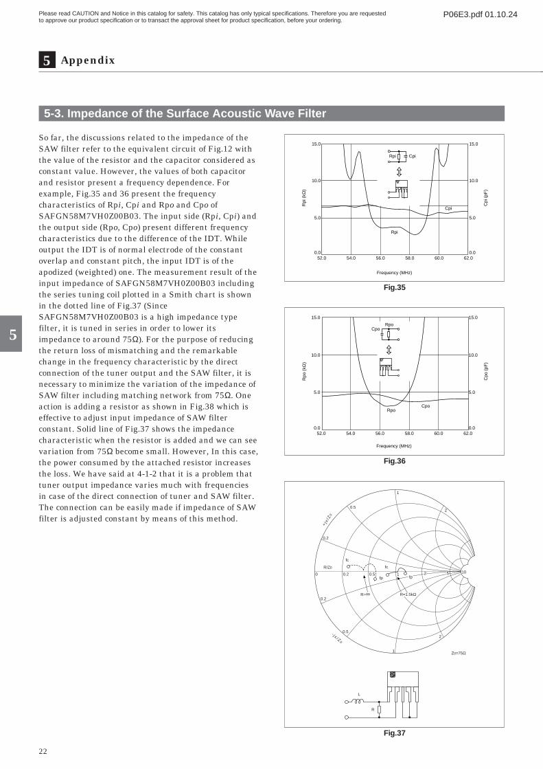
5-3. Impedance of the Surface Acoustic W ave Filter
Fig.35
Rpi Cpi
Rpi
Frequency (MHz)
Rpi
(kΩ
)
Cpi
(pF
)
Cpi
15.0
10.0
5.0
0.0
15.0
10.0
5.0
0.052.0 54.0 56.0 58.0 60.0 62.0
Fig.36
RpoCpo
RpoCpo
Frequency (MHz)
15.0
10.0
5.0
0.0
15.0
10.0
5.0
0.052.0 54.0 56.0 58.0 60.0 62.0
Rpo
(kΩ
)
Cpo
(pF
)
Fig.37
Z0=75Ω1
2
1
2
0.5
0.2
0.5
0.2
0 0.2
R=∞
0.5 1
- j x / Z0
+j x
/ Z0
2 5 10
fc
R/Z0
fp
fc
R=1.5kΩ
fp
R
L
So far, the discussions related to the impedance of theSAW filter refer to the equivalent circuit of Fig.12 withthe value of the resistor and the capacitor considered asconstant value. However, the values of both capacitorand resistor present a frequency dependence. Forexample, Fig.35 and 36 present the frequencycharacteristics of Rpi, Cpi and Rpo and Cpo ofSAFGN58M7VH0Z00B03. The input side (Rpi, Cpi) andthe output side (Rpo, Cpo) present different frequencycharacteristics due to the difference of the IDT. Whileoutput the IDT is of normal electrode of the constantoverlap and constant pitch, the input IDT is of theapodized (weighted) one. The measurement result of theinput impedance of SAFGN58M7VH0Z00B03 includingthe series tuning coil plotted in a Smith chart is shownin the dotted line of Fig.37 (SinceSAFGN58M7VH0Z00B03 is a high impedance typefilter, it is tuned in series in order to lower itsimpedance to around 75Ω). For the purpose of reducingthe return loss of mismatching and the remarkablechange in the frequency characteristic by the directconnection of the tuner output and the SAW filter, it isnecessary to minimize the variation of the impedance ofSAW filter including matching network from 75Ω. Oneaction is adding a resistor as shown in Fig.38 which iseffective to adjust input impedance of SAW filterconstant. Solid line of Fig.37 shows the impedancecharacteristic when the resistor is added and we can seevariation from 75Ω become small. However, In this case,the power consumed by the attached resistor increasesthe loss. We have said at 4-1-2 that it is a problem thattuner output impedance varies much with frequenciesin case of the direct connection of tuner and SAW filter.The connection can be easily made if impedance of SAWfilter is adjusted constant by means of this method.
Please read CAUTION and Notice in this catalog for safety. This catalog has only typical specifications. Therefore you are requestedto approve our product specification or to transact the approval sheet for product specification, before your ordering.
P06E3.pdf 01.10.24
23
5Appendix
5
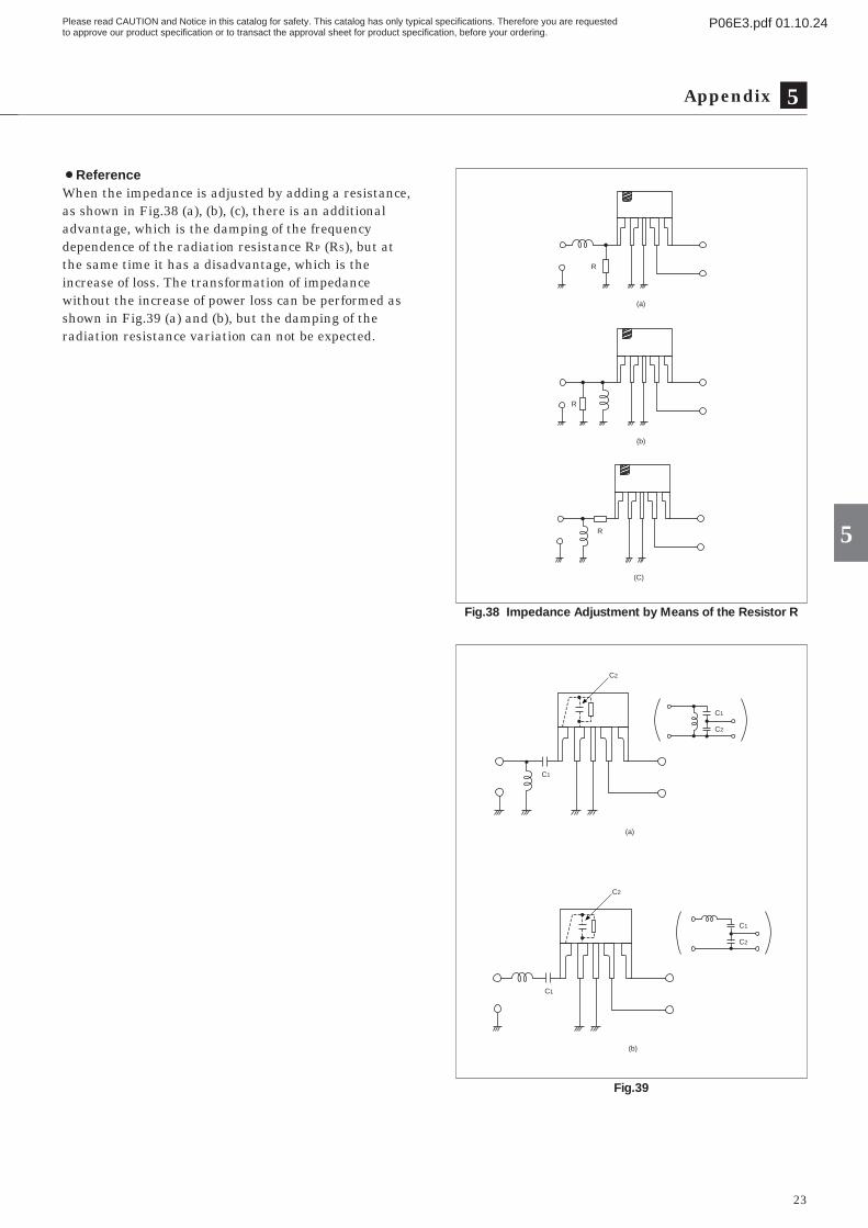
¡ReferenceWhen the impedance is adjusted by adding a resistance,as shown in Fig.38 (a), (b), (c), there is an additionaladvantage, which is the damping of the frequencydependence of the radiation resistance RP (RS), but atthe same time it has a disadvantage, which is theincrease of loss. The transformation of impedancewithout the increase of power loss can be performed asshown in Fig.39 (a) and (b), but the damping of theradiation resistance variation can not be expected.
Fig.38 Impedance Adjustment by Means of the Resistor R
(a)
R
(b)
R
(C)
R
Fig.39
C1
C2
(a)
C1
C2
C1
C2
(b)
C1
C2

Please read CAUTION and Notice in this catalog for safety. This catalog has only typical specifications. Therefore you are requestedto approve our product specification or to transact the approval sheet for product specification, before your ordering.
P06E3.pdf 01.10.24
24
5 Appendix
5
5-4. Reliability T est
Table 5 Limit
Fig.40 Reliability Test Result of SAFGN58M7VH0Z00B03
+0.5
0
-0.5100 500
∆ lo
ss (
dB)
1000 (hrs.)
Humidity Test60°C 95%
100 500 1000 (hrs.)
High Temperature Test85°C
24 48 (hrs.)
Pressure Cooker Test120°C 2 atm
100 (cycle)
+0.5
0
-0.5
∆ fp
(dB
)
+0.5
0
-0.5
∆ fc
(dB
)
+0.5
0
-0.5
∆ fs
(dB
)
Thermal Stress Test-55°C +85°C
Table 4 Reliability Test Conditions
Surface acoustic wave filter should be used carefully notto exceed the maximum rating shown in Table 3 below.Murata performs periodic reliability tests for the SAWfilter. The conditions of them are shown in Table 4. Thedata of SAFGN58M7VH0Z00B03 are shown in Fig.40,which shows that the variation is small enoughcompared to the limit. (Table 5).
Test Items
Vabration
Drop
Lead Pull
Lead Bend
Heat Resistivity for Melt Solder
Soldering
Humidity Test
Thermal Stress Test
High Temperature Test
Low Temperature Test
Test Conditions
600 - 3300 r.p.m.Amplitude (P.P.) 1.5mmX,Y,Z directions, 2h each
100cm, 3 times
1 kg, 15 seconds
0.3kg, 1 return
260˚C, 10 seconds
230˚C 5sec. covered with solder more than 90% of the lead
60˚C, 500 hours, 95% RH
-55˚C 30 min. ¤+85˚C 30 min. 5 cycles
85˚C, 500 hours
-40˚C, 500hours
Table 3 Maximum Ratings
Items
DC Voltage
Pulse Voltage
Input Signal Voltage
Operating Temperature
Storage Temperature
Maximum Rating
10V
150V/200pF
5Vp-p
-20 - +60˚C.
-40 - +85˚C.
Insertion Loss Variation
fp Variation
fc Variation
fs Variation
±1.5dB max.
±1dB max.
±1dB max.
±1.5dB max.

Please read CAUTION and Notice in this catalog for safety. This catalog has only typical specifications. Therefore you are requestedto approve our product specification or to transact the approval sheet for product specification, before your ordering.
P06E3.pdf 01.10.24
25
5Appendix
5
5-5. Notice (handling)
¡Electric characteristics may vary if you use SAW filterwithout cutting off the DC voltage.
¡If static high voltage is applied between inputterminals or output terminals, the SAW filter may bedestroyed.
¡Electric characteristics may vary if the lead is contactwith a heated soldering iron for a long time.
¡Inserting SAW filter in the direction opposite to theinput mark makes frequency characteristicsdisgraded.

Note:1. Export Control
<For customers outside Japan>No muRata products should be used or sold, through any channels, for use in the design, development, production, utilization, maintenance or operation of, orotherwise contribution to (1) any weapons (Weapons of Mass Destruction (nuclear, chemical or biological weapons or missiles) or conventional weapons) or (2)goods or systems specially designed or intended for military end-use or utilization by military end-users.<For customers in Japan>For products which are controlled items subject to the “Foreign Exchange and Foreign Trade Law” of Japan, the export license specified by the law is requiredfor export.
2. Please contact our sales representatives or product engineers before using the products in this catalog for the applications listed below, which require especiallyhigh reliability for the prevention of defects which might directly damage a third party's life, body or property, or when one of our products is intended for use inapplications other than those specified in this catalog.q Aircraft equipment w Aerospace equipmente Undersea equipment r Power plant equipmentt Medical equipment y Transportation equipment (vehicles, trains, ships, etc.)u Traffic signal equipment i Disaster prevention / crime prevention equipmento Data-processing equipment !0 Application of similar complexity and/or reliability requirements to the applications listed above
3. Product specifications in this catalog are as of August 2001. They are subject to change or our products in it may be discontinued without advance notice.Please check with our sales representatives or product engineers before ordering. If there are any questions, please contact our sales representatives orproduct engineers.
4. Please read rating and CAUTION (for storage, operating, rating, soldering, mounting and handling) in this catalog to prevent smoking and/or burning, etc.
5. This catalog has only typical specifications because there is no space for detailed specifications. Therefore, please approve our product specifications ortransact the approval sheet for product specifications before ordering.
6. Please note that unless otherwise specified, we shall assume no responsibility whatsoever for any conflict or dispute that may occur in connection with the effectof our and/or a third party's intellectual property rights and other related rights in consideration of your use of our products and/or information described orcontained in our catalogs. In this connection, no representation shall be made to the effect that any third parties are authorized to use the rights mentionedabove under licenses without our consent.
7. No ozone depleting substances (ODS) under the Montreal Protocol are used in our manufacturing process.
International Division3-29-12, Shibuya, Shibuya-ku, Tokyo 150-0002, Japan Phone: 81-3-5469-6123 Fax: 81-3-5469-6155 E-mail: [email protected]
Head Office1-10-1, Higashi Kotari, Nagaokakyo-shi, Kyoto 617-8555, JapanPhone: 81-75-951-9111
http://www.murata.com/
Please read rating and !CAUTION (for storage, operating, rating, soldering, mounting and handling) in this PDF catalog to prevent smoking and/or burning, etc.This catalog has only typical specifications. Therefore, you are requested to approve our product specifications or to transact the approval sheet for product specificaions before ordering.
!Note P06E3.pdf 01.10.24
Cat. No. P06E-3
Related Documents