Supporting Information High- Efficiency Humidity-Stable Planar Perovskite Solar Cells Based On Atomic Layer Architecture Dibyashree Koushik 1 *, Wiljan J. H. Verhees 2 , Yinghuan Kuang 1 , Sjoerd Veenstra 2 , Dong Zhang 2 , Marcel A. Verheijen 1,3 , Mariadriana Creatore 1,2 , and Ruud E.I. Schropp 1,2 1 Plasma and Materials Processing, Department of Applied Physics, Eindhoven University of Technology (TU/e), 5600 MB Eindhoven, The Netherlands 2 ECN-Solliance, High Tech Campus 21, 5656AE Eindhoven, The Netherlands 3 Philips Innovation Labs, High Tech Campus 11, 5656 AE Eindhoven, The Netherlands Electronic Supplementary Material (ESI) for Energy & Environmental Science. This journal is © The Royal Society of Chemistry 2016

Welcome message from author
This document is posted to help you gain knowledge. Please leave a comment to let me know what you think about it! Share it to your friends and learn new things together.
Transcript
Supporting Information
High- Efficiency Humidity-Stable Planar Perovskite Solar Cells
Based On Atomic Layer Architecture
Dibyashree Koushik1*, Wiljan J. H. Verhees2, Yinghuan Kuang1, Sjoerd Veenstra2, Dong
Zhang2, Marcel A. Verheijen1,3, Mariadriana Creatore 1,2, and Ruud E.I. Schropp1,2
1Plasma and Materials Processing, Department of Applied Physics, Eindhoven University of
Technology (TU/e), 5600 MB Eindhoven, The Netherlands 2ECN-Solliance, High Tech Campus 21, 5656AE Eindhoven, The Netherlands
3Philips Innovation Labs, High Tech Campus 11, 5656 AE Eindhoven, The Netherlands
Electronic Supplementary Material (ESI) for Energy & Environmental Science.This journal is © The Royal Society of Chemistry 2016
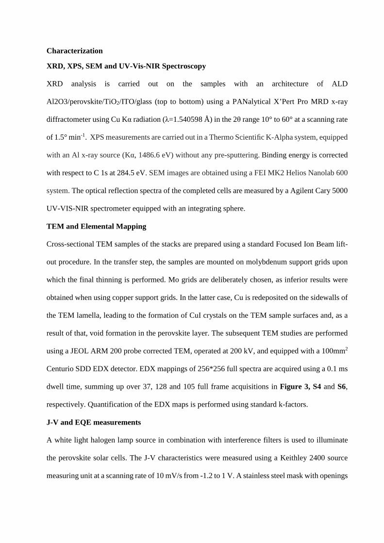
Characterization
XRD, XPS, SEM and UV-Vis-NIR Spectroscopy
XRD analysis is carried out on the samples with an architecture of ALD
Al2O3/perovskite/TiO2/ITO/glass (top to bottom) using a PANalytical X’Pert Pro MRD x-ray
diffractometer using Cu Kα radiation (λ=1.540598 Å) in the 2θ range 10° to 60° at a scanning rate
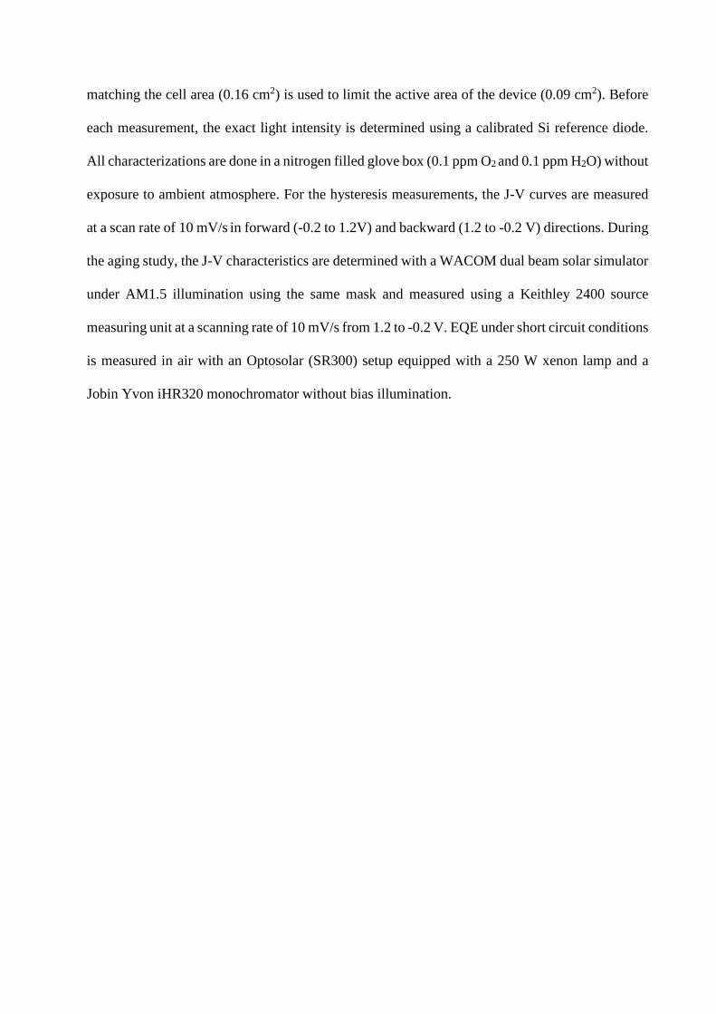
of 1.5° min-1. XPS measurements are carried out in a Thermo Scientific K-Alpha system, equipped
with an Al x-ray source (Kα, 1486.6 eV) without any pre-sputtering. Binding energy is corrected
with respect to C 1s at 284.5 eV. SEM images are obtained using a FEI MK2 Helios Nanolab 600
system. The optical reflection spectra of the completed cells are measured by a Agilent Cary 5000
UV-VIS-NIR spectrometer equipped with an integrating sphere.
TEM and Elemental Mapping
Cross-sectional TEM samples of the stacks are prepared using a standard Focused Ion Beam lift-
out procedure. In the transfer step, the samples are mounted on molybdenum support grids upon
which the final thinning is performed. Mo grids are deliberately chosen, as inferior results were
obtained when using copper support grids. In the latter case, Cu is redeposited on the sidewalls of
the TEM lamella, leading to the formation of CuI crystals on the TEM sample surfaces and, as a
result of that, void formation in the perovskite layer. The subsequent TEM studies are performed
using a JEOL ARM 200 probe corrected TEM, operated at 200 kV, and equipped with a 100mm2
Centurio SDD EDX detector. EDX mappings of 256*256 full spectra are acquired using a 0.1 ms
dwell time, summing up over 37, 128 and 105 full frame acquisitions in Figure 3, S4 and S6,
respectively. Quantification of the EDX maps is performed using standard k-factors.
J-V and EQE measurements
A white light halogen lamp source in combination with interference filters is used to illuminate
the perovskite solar cells. The J-V characteristics were measured using a Keithley 2400 source
measuring unit at a scanning rate of 10 mV/s from -1.2 to 1 V. A stainless steel mask with openings
matching the cell area (0.16 cm2) is used to limit the active area of the device (0.09 cm2). Before
each measurement, the exact light intensity is determined using a calibrated Si reference diode.
All characterizations are done in a nitrogen filled glove box (0.1 ppm O2 and 0.1 ppm H2O) without
exposure to ambient atmosphere. For the hysteresis measurements, the J-V curves are measured
at a scan rate of 10 mV/s in forward (-0.2 to 1.2V) and backward (1.2 to -0.2 V) directions. During
the aging study, the J-V characteristics are determined with a WACOM dual beam solar simulator
under AM1.5 illumination using the same mask and measured using a Keithley 2400 source
measuring unit at a scanning rate of 10 mV/s from 1.2 to -0.2 V. EQE under short circuit conditions
is measured in air with an Optosolar (SR300) setup equipped with a 250 W xenon lamp and a
Jobin Yvon iHR320 monochromator without bias illumination.
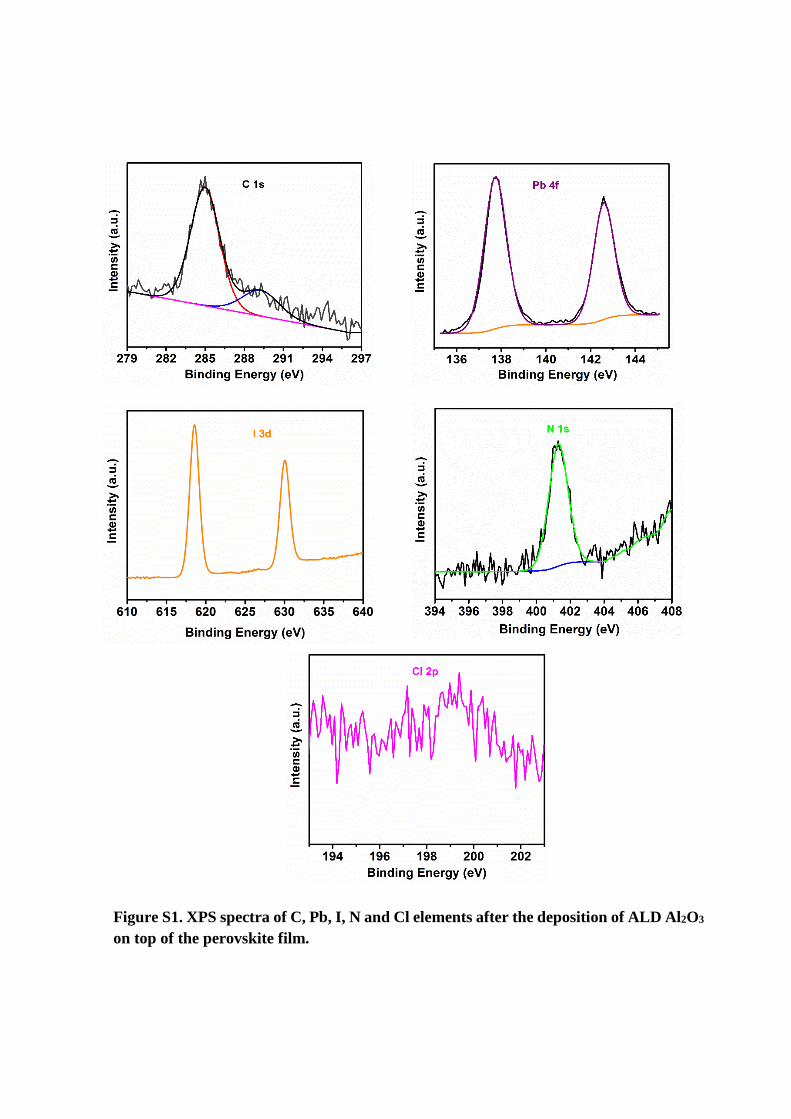
Figure S1. XPS spectra of C, Pb, I, N and Cl elements after the deposition of ALD Al2O3 on top of the perovskite film.
Figure S2. Top view SEM image of the perovskite film.

Figure S3. Box plot showing the PV parameters of the perovskite devices employing different cycles of ALD Al2O3 at the perovskite/HTL interface.

Figure S4. High angle annular dark field (HAADF) scanning TEM image of the device layer stack and the corresponding individual and overlapped elemental maps of Al, O, Pb, I, C, N, Ti and In and Au.
CH3NH3PbI3-δClδ
Spiro-OMeTAD
Au
c-TiO2 ITO
Glass

Figure S5. Reflectance spectra of the perovskite devices with and without the ALD Al2O3.

Figure S6. High angle annular dark field (HAADF) scanning TEM image of the device layer stack and the corresponding individual and overlapped elemental maps of Al, O, Pb, I, C, Ti and In.
Spiro-OMeTAD
CH3NH3PbI3-δClδ
c-TiO2
ITO
Glass
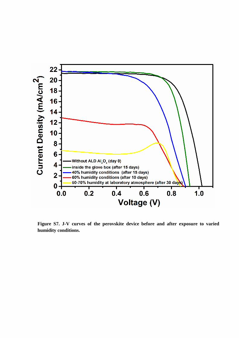
Figure S7. J-V curves of the perovskite device before and after exposure to varied humidity conditions.
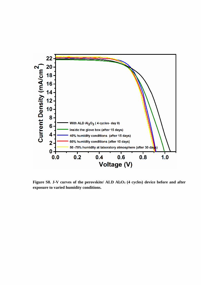
Figure S8. J-V curves of the perovskite/ ALD Al2O3 (4 cycles) device before and after exposure to varied humidity conditions.
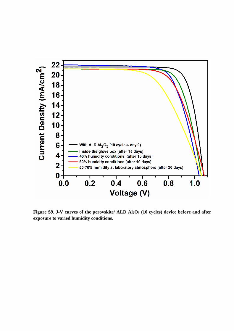
Figure S9. J-V curves of the perovskite/ ALD Al2O3 (10 cycles) device before and after exposure to varied humidity conditions.
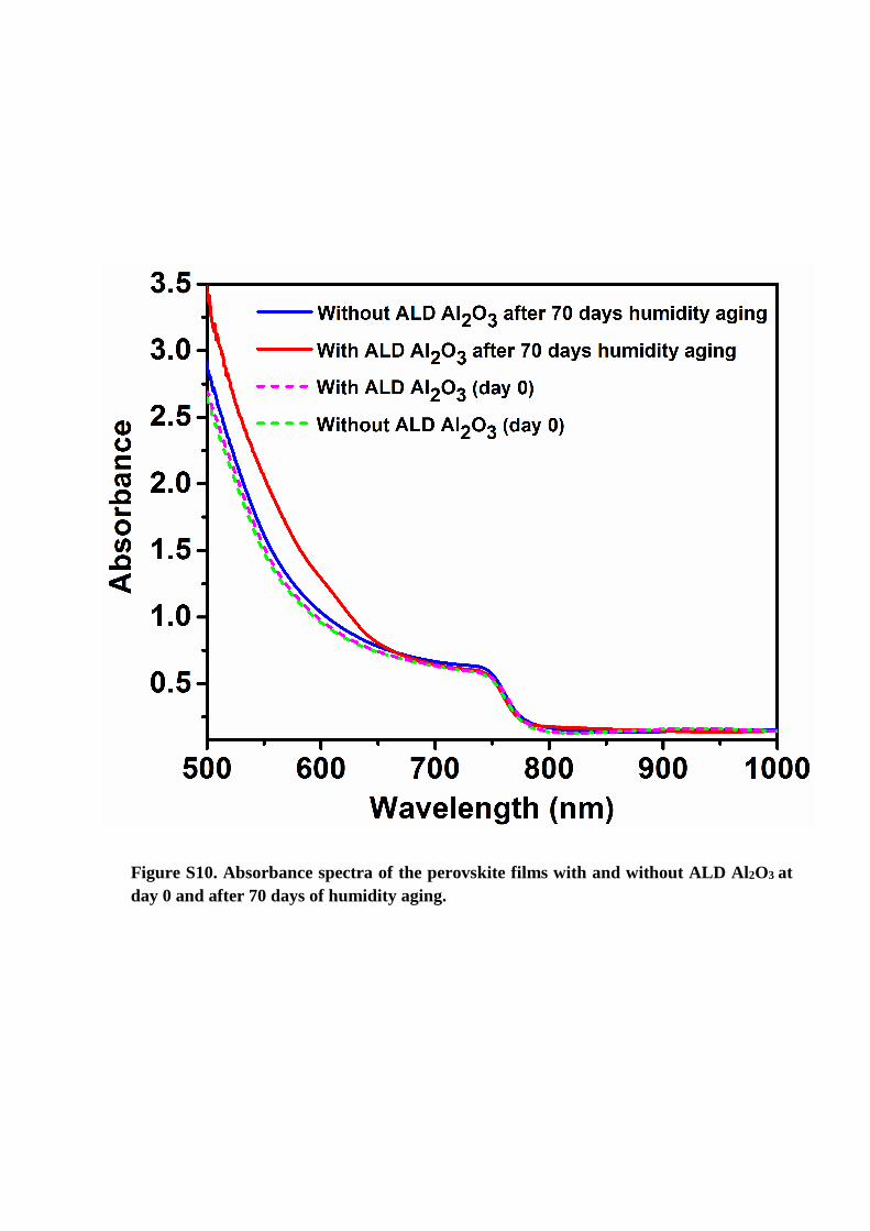
Figure S10. Absorbance spectra of the perovskite films with and without ALD Al2O3 at day 0 and after 70 days of humidity aging.
Related Documents