SUPPORT OF FMA IN OPEN-SOURCE PROCESSOR By Ahmed Ali Ismail Ali Mohamed A Thesis Submitted to the Faculty of Engineering at Cairo University in Partial Fulfillment of the Requirements for the Degree of MASTER OF SCIENCE in ELECTRONICS AND COMMUNICATIONS ENGINEERING FACULTY OF ENGINEERING, CAIRO UNIVERSITY GIZA, EGYPT 2016

Welcome message from author
This document is posted to help you gain knowledge. Please leave a comment to let me know what you think about it! Share it to your friends and learn new things together.
Transcript
SUPPORT OF FMA IN OPEN-SOURCE PROCESSOR
By
Ahmed Ali Ismail Ali Mohamed
A Thesis Submitted to the
Faculty of Engineering at Cairo University
in Partial Fulfillment of the
Requirements for the Degree of
MASTER OF SCIENCE
in
ELECTRONICS AND COMMUNICATIONS ENGINEERING
FACULTY OF ENGINEERING, CAIRO UNIVERSITY
GIZA, EGYPT
2016

SUPPORT OF FMA IN OPEN-SOURCE PROCESSOR
By
Ahmed Ali Ismail Ali Mohamed
A Thesis Submitted to the
Faculty of Engineering at Cairo University
in Partial Fulfillment of the
Requirements for the Degree of
MASTER OF SCIENCE
in
ELECTRONICS AND COMMUNICATIONS ENGINEERING
Under the Supervision of
Prof. Dr. Hossam A. H. Fahmy
Professor, Electronics and Communications
Engineering, Faculty of Engineering, Cairo University
FACULTY OF ENGINEERING, CAIRO UNIVERSITY
GIZA, EGYPT
2016

SUPPORT OF FMA IN OPEN-SOURCE PROCESSOR
By
Ahmed Ali Ismail
A Thesis Submitted to the
Faculty of Engineering at Cairo University
in Partial Fulfillment of the
Requirements for the Degree of
MASTER OF SCIENCE
in
ELECTRONICS AND COMMUNICATIONS ENGINEERING
Approved by the
Examining Committee
____________________________
Prof. Dr. Hossam A. H. Fahmy, Thesis Main Advisor
____________________________
Prof. Dr. Ibrahim Mohamed Qamar, Internal Examiner
____________________________
Prof. Dr. Ashraf M. Salem, External Examiner (Faculty of Engineering, Ain Shams University)
FACULTY OF ENGINEERING, CAIRO UNIVERSITY
GIZA, EGYPT
2016
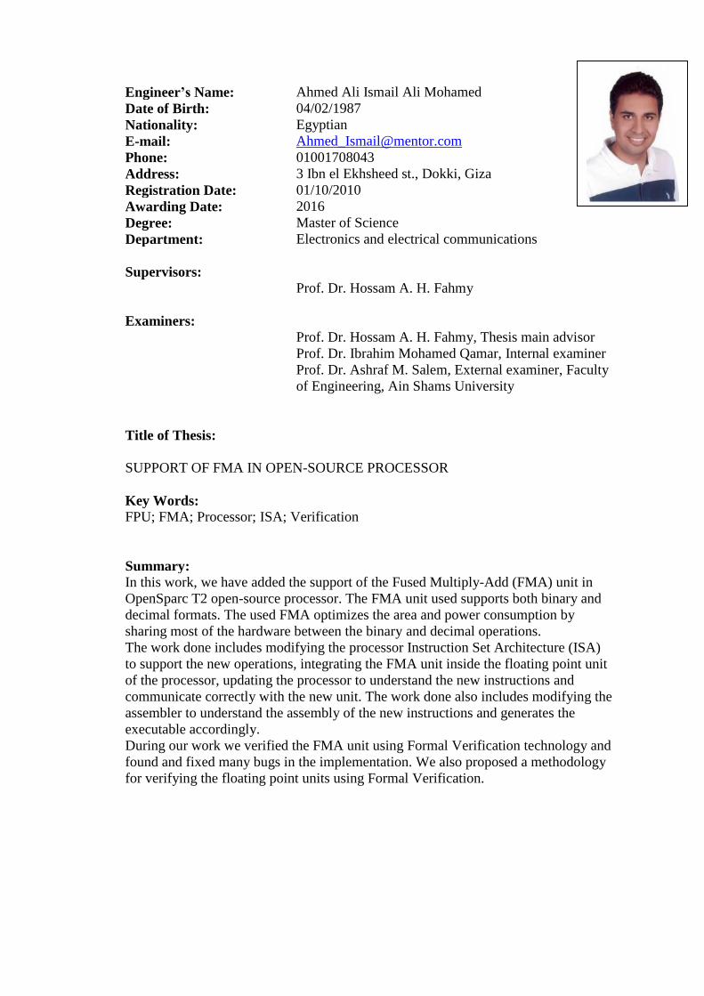
Engineer’s Name: Ahmed Ali Ismail Ali Mohamed
Date of Birth: 04/02/1987
Nationality: Egyptian
E-mail: [email protected]
Phone: 01001708043
Address: 3 Ibn el Ekhsheed st., Dokki, Giza
Registration Date: 01/10/2010
Awarding Date: 2016
Degree: Master of Science
Department: Electronics and electrical communications
Supervisors:
Prof. Dr. Hossam A. H. Fahmy
Examiners:
Prof. Dr. Hossam A. H. Fahmy, Thesis main advisor
Prof. Dr. Ibrahim Mohamed Qamar, Internal examiner
Prof. Dr. Ashraf M. Salem, External examiner, Faculty
of Engineering, Ain Shams University
Title of Thesis:
SUPPORT OF FMA IN OPEN-SOURCE PROCESSOR
Key Words:
FPU; FMA; Processor; ISA; Verification
Summary:
In this work, we have added the support of the Fused Multiply-Add (FMA) unit in
OpenSparc T2 open-source processor. The FMA unit used supports both binary and
decimal formats. The used FMA optimizes the area and power consumption by
sharing most of the hardware between the binary and decimal operations.
The work done includes modifying the processor Instruction Set Architecture (ISA)
to support the new operations, integrating the FMA unit inside the floating point unit
of the processor, updating the processor to understand the new instructions and
communicate correctly with the new unit. The work done also includes modifying the
assembler to understand the assembly of the new instructions and generates the
executable accordingly.
During our work we verified the FMA unit using Formal Verification technology and
found and fixed many bugs in the implementation. We also proposed a methodology
for verifying the floating point units using Formal Verification.

i
Acknowledgments
Praise be to Allah, Lord of the Worlds for all his blessings, and peace be upon
prophet Mohamed and his companions.
I want to thank my family and wife for their invaluable support. Also thanks to all
my friends for their help and support.
Finally, I would like to express my sincere gratitude to my advisor Prof. Hossam
Fahmy for his support, patience and encouragement.

ii
Table of Contents
ACKNOWLEDGMENTS ............................................................................................. I
TABLE OF CONTENTS .............................................................................................. II
LIST OF TABLES ........................................................................................................ V
LIST OF FIGURES .....................................................................................................VI
ABSTRACT ................................................................................................................ VII
CHAPTER 1 : INTRODUCTION ................................................................................ 1
1.1. FLOATING POINT ARITHMETIC .............................................................. 1
1.2. BINARY FLOATING POINT ARITHMETIC ................................................. 1
1.3. DECIMAL FLOATING POINT ARITHMETIC .............................................. 2
1.4. IEEE STANDARD FOR FLOATING POINT ARITHMETIC ............................ 2
1.4.1. Binary floating point numbers representation ......................................... 2
1.4.2. Decimal floating point numbers representation ...................................... 4
1.4.3. Special values .......................................................................................... 5
1.4.4. Flags and exceptions ............................................................................... 5 1.4.4.1. Invalid operation ........................................................................................................ 5 1.4.4.2. Division by zero ......................................................................................................... 6 1.4.4.3. Overflow .................................................................................................................... 6 1.4.4.4. Underflow .................................................................................................................. 6 1.4.4.5. Inexact........................................................................................................................ 6
1.4.5. Rounding ................................................................................................. 6
1.5. THESIS ORGANIZATION ........................................................................ 7
CHAPTER 2 : FLOATING POINT FUSED MULTIPLY-ADD UNIT ................... 9
2.1. FMA BASIC BLOCKS ............................................................................ 9
2.2. FMA UNIT DESCRIPTION .................................................................... 10
2.3. DECODING THE INPUTS ....................................................................... 10
2.4. MULTIPLICATION ............................................................................... 12
2.4.1. Partial products generation .................................................................... 13 2.4.1.1. Decimal partial products generation ........................................................................ 13 2.4.1.2. Binary partial products generation ........................................................................... 15
2.4.2. Partial products reduction ..................................................................... 18
2.5. PREPARING THE ADDEND ................................................................... 19
2.6. CARRY SAVE ADDER .......................................................................... 22
2.7. LEADING ZEROS ANTICIPATION.......................................................... 22
2.8. REDUNDANT ADDER ........................................................................... 22
2.8.1. Conversion from Binary/Decimal to Redundant ................................... 22
2.8.2. Redundant addition ............................................................................... 24
2.9. NORMALIZATION SHIFTING ................................................................ 25
2.10. ROUNDING ........................................................................................ 25
2.11. FMA UNIT CONCLUSION ................................................................... 25

iii
CHAPTER 3 : FMA UNIT VERIFICATION ........................................................... 27
3.1. FMA UNIT INITIAL VERIFICATION ...................................................... 27
3.2. FMA UNIT EXTENDED VERIFICATION ................................................. 27
3.2.1. FPU verification techniques and challenges ......................................... 27 3.2.1.1. FPU simulation based verification ........................................................................... 28 3.2.1.2. FPU Formal verification .......................................................................................... 28
3.3. APPLYING SIMULATION TEST VECTORS ON THE FMA UNIT ................ 30
3.4. APPLYING DESIGN CHECKS ON THE FMA UNIT .................................. 31
3.5. FORMALLY VERIFYING FMA FUNCTIONALITY ................................... 35
3.5.1. Testing the overall FMA functionality .................................................. 35 3.5.1.1. Formal verification tool ........................................................................................... 35 3.5.1.2. SystemVerilog language .......................................................................................... 36 3.5.1.3. Defining system properties ...................................................................................... 36
3.5.2. Testing the FMA building blocks ......................................................... 40 3.5.2.1. Verifying the binary carry save adder (CSA) ........................................................... 41 3.5.2.2. Debugging the final binary exponent calculation unit .............................................. 41
3.6. NEW PROPOSED VERIFICATION FLOW FOR THE FLOATING POINT UNITS
43
3.6.1. Testing and debugging the FMA unit ................................................... 43
3.6.2. Verifying the overall functionality of the FMA unit as a black box
testing 44
3.7. FIXING FMA DESIGN FUNCTIONALITY ............................................... 48
3.8. RE-VERIFYING THE DESIGN ................................................................ 49
3.9. VERIFYING OTHER FP MULTIPLIERS USING OUR DEVELOPED CHECKER
49
3.10. CONCLUSION .................................................................................... 50
CHAPTER 4 : OPENSPARC T2 PROCESSOR ...................................................... 51
4.1. OPENSPARC T2 PROCESSOR OVERVIEW ............................................. 51
4.2. INSTRUCTION FETCH UNIT (IFU) ........................................................ 51
4.2.1. Fetch unit .............................................................................................. 51
4.2.2. Pick unit ................................................................................................ 52
4.2.3. Decode unit ........................................................................................... 53
4.3. EXECUTION UNIT ................................................................................ 55
4.4. LOAD STORE UNIT ............................................................................. 56
4.5. CACHE CROSSBAR ............................................................................. 56
4.6. MEMORY MANAGEMENT UNIT .......................................................... 56
4.7. TRAP LOGIC UNIT .............................................................................. 57
4.8. FLOATING POINT UNIT ....................................................................... 60
4.8.1. Interface with other units ...................................................................... 62
4.8.2. Floating-Point State Register (FSR)...................................................... 63
4.8.3. Conclusion ............................................................................................ 64
CHAPTER 5 : INCLUDING THE BINARY/DECIMAL FMA IN THE
OPENSPARC T2 PROCESSOR ................................................................................ 65
5.1. RELATED WORK ................................................................................. 65

iv
5.2. SPARC ISA UPDATE ......................................................................... 66
5.3. FGU CHANGES ................................................................................... 68
5.4. GASKET CHANGES .............................................................................. 69
5.5. PICK UNIT CHANGES ........................................................................... 69
5.6. DECODE UNIT CHANGES ..................................................................... 70
5.7. TLU UNIT CHANGES ........................................................................... 70
5.8. SOFTWARE CHANGES ......................................................................... 70
5.8.1. include/opcode/sparc.h changes ............................................................ 71
5.8.2. opcodes/sparc-opc.c changes ................................................................ 72
5.8.3. gas/config/tc-sparc.c changes ................................................................ 73
5.9. FMA AREA CALCULATION ................................................................. 74
CHAPTER 6 : CONCLUSION AND FUTURE WORK .......................................... 75
REFERENCES ............................................................................................................. 76

v
List of Tables
Table 1.1: Binary floating point formats .......................................................................... 2 Table 1.2: Binary special values encodings ..................................................................... 3 Table 1.3: Decimal floating point formats ....................................................................... 4 Table 1.4: Decimal to declet conversion .......................................................................... 5 Table 2.1: selop signal decoding .................................................................................... 12
Table 2.2: round signal decoding ................................................................................... 12 Table 2.3: Decimal digit encoding in Radix-5 format .................................................... 13
Table 2.4: Decimal digit selection bits in Radix-5 format ............................................. 14
Table 2.5: Binary selection bits in Radix-4 format ........................................................ 17 Table 2.6: Decimal to redundant conversion .................................................................. 23 Table 2.7: Binary to redundant conversion .................................................................... 24 Table 3.1: Initial simulation results for the FMA unit ................................................... 31 Table 3.2: Design issues in the FMA unit ...................................................................... 31
Table 3.3: Test vector causing sNaN value to appear on the FMA output .................... 39
Table 3.4: Test vector causing assertion firing ............................................................... 40 Table 3.5: Test vector causing wrong flags values ......................................................... 42
Table 3.6: Test vector causing wrong unexpected FP result .......................................... 48 Table 3.7: Test vector causing wrong FP multiplier result ............................................ 49 Table 3.8: Test vector causing wrong FP multiplier result ............................................ 49
Table 4.1: OpenSparc T2 hazards .................................................................................. 53
Table 4.2: FGU clock domains ....................................................................................... 63 Table 5.1: Opcode for the implementation dependent instructions ................................ 66 Table 5.2: Op3 values for IMPDEP1 and IMPDEP2 ..................................................... 66
Table 5.3: Op3 values for IMPDEP1 and IMPDEP2 ..................................................... 66 Table 5.4: Opcode for the FMA instructions.................................................................. 66
Table 5.5: Op5 values for FMA operations .................................................................... 67 Table 5.6: Opcode for IMPDEP1 ................................................................................... 67 Table 5.7: Opf values for decimal operations ................................................................ 67 Table 5.8: FGU Area profile .......................................................................................... 74

vi
List of Figures
Figure 1.1: Binary floating point encoding ...................................................................... 3 Figure 1.2: Decimal floating point encoding .................................................................... 4 Figure 2.1: FMA block diagram ..................................................................................... 11 Figure 2.2: Final decimal partial product tree ................................................................ 15 Figure 2.3: Final binary partial products tree ................................................................. 18
Figure 2.4: Decimal shift cases ...................................................................................... 20 Figure 2.5: Binary shift cases ......................................................................................... 21
Figure 2.6: Procedure for converting to redundant ........................................................ 23
Figure 2.7: Procedure redundant addition ...................................................................... 25 Figure 3.1: Fixing undriven signal issue ........................................................................ 32 Figure 3.2: Latch inferred due to wrong coding style .................................................... 32 Figure 3.3: Fixing the coding style to avoid inferring latch in the design...................... 33 Figure 3.4: Combinational loop issue in the design ....................................................... 33
Figure 3.5: Fixing the combinational loop issue ............................................................ 33
Figure 3.6: Unreachable block of code issue .................................................................. 34 Figure 3.7: Optimizing the design by removing the unreachable code block ................ 34
Figure 3.8: Fixing the missing conditions in the case statement .................................... 35 Figure 3.9: Specifying cover directives to verify that the output signals can toggle ..... 37 Figure 3.10: Checks for the binary floating point output variations .............................. 38
Figure 3.11: Assertions to verify the basic properties identified for the flags ............... 40
Figure 3.12: Assertions to verify the binary CSA block ................................................ 41 Figure 3.13: Assertion used to verify the final exponent calculation unit ...................... 42 Figure 3.14: Using assumption to direct the Formal to run on a specific scenario ........ 43
Figure 3.15: Using assertion to verify overflow calculation .......................................... 43 Figure 3.16: FPU verification checker ........................................................................... 45
Figure 3.17: FPU verification checker workflow ........................................................... 47 Figure 4.1: OpenSparc T2 Core block diagram .............................................................. 52 Figure 4.2: Timing diagram for handling dependent instructions .................................. 54 Figure 4.3: EXU block diagram ..................................................................................... 55
Figure 4.4: Communication between the SPARC core and the L2 cache through the
cache crossbar ................................................................................................................. 56
Figure 4.5: TLU basic blocks ......................................................................................... 57 Figure 4.6: Correct trap prediction ................................................................................. 59 Figure 4.7: Trap mis-prediction ...................................................................................... 60 Figure 4.8: FGU block diagram...................................................................................... 61 Figure 4.9: FGU pipelines .............................................................................................. 62
Figure 4.10: FGU interface with other units .................................................................. 63 Figure 5.1: include/opcode/sparc.h changes ................................................................... 72 Figure 5.2: opcodes/sparc-opc.c changes ....................................................................... 72 Figure 5.3: gas/config/tc-sparc.c changes ...................................................................... 74
vii
Abstract
In this work, we have added the support of the Fused Multiply-Add (FMA) unit in
OpenSparc T2 open-source processor. The FMA unit used supports both binary and
decimal formats, allowing us to complete the support for the binary floating point
operations in the aforementioned processor since it was missing the FMA operations as
well as adding initial support for decimal floating point operations which were totally
missing in the processor. The used FMA optimizes the area and power consumption by
sharing most of the hardware between the binary and decimal operations.
The support of more functionality on the processor hardware helps in improving the
overall processing time, compared to the software implementations of the same
functionality where the unsupported hardware instruction is replaced by multiple simpler
instructions. The area considerations for the new hardware support can be minimized by
optimizing the hardware implementation and reusing the hardware units in different
operations. Also using newer technology with smaller feature size can reduce the overall
area needed.
The work done includes modifying the processor Instruction Set Architecture (ISA)
to support the new operations, integrating the FMA unit inside the floating point unit of
the processor, updating the processor to understand the new instructions and
communicate correctly with the new unit. The work done also includes modifying the
assembler to understand the assembly of the new instructions and generates the
executable accordingly.
The new functionality of the processor is verified by updating the processor testing
environment with new tests to exercise the new instructions, the old functionality of the
processor is also verified in the different scenarios by using the processor available
regression tests.
During our work we verified the FMA unit using Formal Verification technology
and found and fixed many bugs in the implementation. We also proposed a methodology
for verifying the floating point units using Formal Verification.

1
Chapter 1 : Introduction
1.1. Floating point arithmetic
The floating point arithmetic is used in many applications that require complex
calculations and accurate results with large dynamic range. The fixed point arithmetic
although much simpler and can use the integer units in the processor, but it supports very
small range of numbers. For the same number of bits, the fixed point numbers have a
choice of either precision or supporting large numbers while floating point numbers can
support both. Taking an eight bits number as an example, only 256 different numbers can
be represented in either fixed or floating point numbers, the selection of the fixed point
location will limit both the range and precision of the number to a fixed value. Assuming
the point position is selected to be 2 bits from the right, then the maximum fixed point
number is 64 and the precision is 0.25. On the other side if we defined a floating point
number with 2 bits to define the point position within the least significant 6 bits then we
can reach the same maximum value but with higher precision of 0.0625. The floating
point benefits will come with the cost of adding extra complexity in the calculations
which turns into extra delay and larger hardware area.
Floating point operations can be done on any processor even if the processor has no
floating point support on the hardware. However, the usage of the software libraries to
perform the floating point operations slows down the computation. A dedicated floating
point unit (FPU) is supported in many processors today since doing the operation on
hardware saves both time and power [1].
Benchmarking for the support of decimal floating point (DFP) in hardware versus
the support in software has been done in [2], authors have concluded that large
improvement in the DFP applications is achieved when having the support in hardware.
The benchmark results showed that more than 75% of the execution time is spent in DFP
functions if evaluated in software. The hardware support speedup ranges from 1.3 to 31.2
on different benchmarks. In [3] the energy-delay product improvement due to the use of
hardware support was reported over 500.
1.2. Binary floating point arithmetic
The binary floating point (BFP) units have been available in commercial computers
since 1950’s [4]. The numbers in BFP format are represented by three parts: sign,
exponent and mantissa. The mantissa is similar to the integer representation and therefore
can use the same integer units or techniques for the mantissa calculations. In fact in some
processors such as the OpenSparc T2 processor, as we will explain in more details in
Chapter 4, the integer and binary floating point multiplication and division are sharing
the same units.

2
1.3. Decimal floating point arithmetic
The main limitation for the BFP arithmetic is the ability to handle the common
fractions accurately. The common fraction 0.1 as an example cannot be described
accurately using BFP number using finite number of bits. This limitation may cause a
large errors in some of the financial applications causing large loss for the companies due
to truncation error [5]
Therefore the increasing demand on DFP arithmetic is more obvious in military and
financial applications.
1.4. IEEE standard for floating point arithmetic
The floating point arithmetic standard (IEEE 754) was published in 1985 and
updated in 2008 (IEEE 754-2008) [6]. The standard was defined to make sure that the
results are correct and consistent if the operation is done through hardware unit, software
library, or combination of both. The software development can be compatible across
different machines if the operations are following the standard. The standard specifies
binary and decimal formats for the floating point numbers. The standard specifies five
basic formats which are three binary formats with encodings of lengths 32, 64, and 128
bits (also known as single, double and quad precisions) and two decimal formats with
encodings in lengths of 64 and 128 bits. The standard also specifies possible extensions
to these formats.
The floating point numbers are defined in the following form:(−1)s x be x m, where
s is the sign and can take values 0 or 1, b is the radix and can be either 2 for binary and
10 for decimal, e is the exponent and can be any integer between emin and emax (the
emin and emax varies from one format to another but will always follow the rule that
emin = 1 – emax), and m is the significand of the number. The number of bits in the
significand is the precision (p) and the values of each digit in the significand is between
0 and b. The standard defines +ve and –ve zeros. Beside that the standard specifies four
more floating point values which are two infinities (+∞ and −∞) and two Not a Number
(NaNs) which are qNaN (quiet) and sNaN (signaling).
1.4.1. Binary floating point numbers representation
The binary floating point numbers have the radix of 2. The basic binary floating point
formats defined in the standard are represented in Table 1.1
Table 1.1: Binary floating point formats
Parameter Binary 32 Binary 64 Binary 128
Precision (p) 24 53 113
Emax 127 1023 16383
exponent field width 8 11 15
The encoding for the binary number in each format is unique, i.e. each number can
be represented in only one possible encoding. The binary numbers encoding is shown in

3
Figure 1.1 where the most significant bit (MSB) represents the sign, the next w bits are
representing the biased exponent, and the least significant p-1 bits are used for the trailing
significand. The biased exponent is defined as E = e + bias where bias is fixed number
for every binary format which is equal to emax. The MSB of the significand is hidden so
the total number of bits for the significand is p. The hidden bit can be either 0 or 1
according to the exponent value, those are called normal and subnormal numbers
respectively.
Figure 1.1: Binary floating point encoding
The exponent for normal binary floating point numbers is in the range 1 to 2𝑤 − 2,
the remaining two values for the exponent which are 0 and 2𝑤 − 1 are reserved for the
following special representations:
1. E = 0 is used to encode ±0 and the subnormal numbers
2. E = 2𝑤 − 1 is used to encode ±∞ and the NaNs
The normal binary floating point numbers have a hidden 1 in the significand and are
represented as (−1)s x 2ex 1. significand, the largest number that can be represented in
this format is (−1)s x 22w−2x 1. 2𝑝−1 while the smallest normal binary floating point
number is represented by E=1 and trailing significand (T) = 0 and is equivalent to
(−1)s x 21−bias . The numbers smaller than the smallest normal values are called
subnormal and have leading hidden 0, with the exponent bits are all zeros. The maximum
subnormal number is (−1)s x 2−𝑏𝑖𝑎𝑠x 0. 2𝑝−1.
Because of the hidden 1 in the normal binary numbers, the binary operations requires
normalization step at the end to bring the result back to the normal form in case the result
is not subnormal, this is not always needed in the decimal operations since the result can
be un-normalized as shown in next section.
The biased exponent E = 2𝑤 − 1 is used to represent special values as shown in
Table 1.2
Table 1.2: Binary special values encodings
Significand Special value
= 0 ±∞
≠ 0 qNaN, or sNaN
The 0 binary number is represented by the encoding of E = 0 and T = 0. The standard
supports ±0 which is useful in case of division by zero to identify of the result is +ve or
–ve ∞.

4
1.4.2. Decimal floating point numbers representation
The decimal floating point numbers have the radix of 10. The decimal floating point
numbers are more convenient in some applications like the financial and military
applications where the error impact can be very large. The decimal floating point
numbers are more familiar to the human since it is used in the their normal operations,
the decimal floating point numbers can also specify some numbers that the binary cannot
specify accurately in finite number of bits such as the number 0.1.
The IEEE 754-2008 added support for the decimal floating point arithmetic, the
standard specifies two basic encodings for the decimal formats as explained in Table 1.3.
Table 1.3: Decimal floating point formats
Parameter Decimal 64 Decimal 128
Precision (p) 16 34
emax 384 6144
combination field width in bits 13 17
The decimal encoding -unlike the binary one- allows multiple representation for the
value, all the representations for the same value are called cohort. The different encodings
for the same decimal number allows the system to maintain the precision of the result,
for example the two numbers 5 x 10⁻² and 50 x 10−3are equivalent but the precision in
the second number is greater by 1 digit. The number of available cohorts for each values
varies according to the number of trailing zeros in the value as well as the difference
between exponent and the maximum and minimum exponents. The maximum number of
cohorts for decimal floating point number is equal to the number of digits in the
significand of this number. The standard specifies the preferred exponent -out of all the
available cohorts- of the number for each operation to make sure that results are
consistent across the different implementations.
The decimal numbers encoding is shown in Figure 1.2, the MSB of the number is
the sign bit, the next w+5 bits (G) are representing the exponent and the last t trailing bits
are representing the trailing significand (T).
Figure 1.2: Decimal floating point encoding
The standard specifies two ways to encode the significand, the first one is the decimal
encoding using densely-packed-decimal encoding, the other way is to use binary
encoding and consider all the t significand bits as one integer value with range from 0 to
2𝑡 − 1 . The binary encoding can be used efficiently if the decimal floating point
operations are done on the software since the operations can reuse the integer execution
5
units, while the densely-packed-decimal is more efficient in the hardware
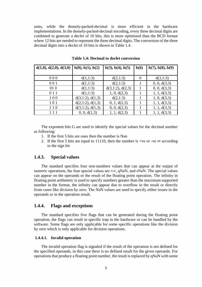
implementations. In the densely-packed-decimal encoding, every three decimal digits are
combined to generate a declet of 10 bits, this is more optimized than the BCD format
where 12 bits are needed to represent the three decimal digits. The conversion of the three
decimal digits into a declet of 10 bits is shown in Table 1.4.
Table 1.4: Decimal to declet conversion
d(1,0), d(2,0), d(3,0) b(0), b(1), b(2) b(3), b(4), b(5) b(6) b(7), b(8), b(9)
0 0 0 d(1,1:3) d(2,1:3) 0 d(3,1:3)
0 0 1 d(1,1:3) d(2,1:3) 1 0, 0, d(3,3)
01 0 d(1,1:3) d(3,1:2), d(2,3) 1 0, 0, d(3,3)
0 1 1 d(1,1:3) 1, 0, d(2,3) 1 1, 1, d(3,3)
1 0 0 d(3,1:2), d(1,3) d(2,1:3) 1 1, 0, d(3,3)
1 0 1 d(2,1:2), d(1,3) 0, 1, d(2,3) 1 1, 1, d(3,3)
1 1 0 d(3,1:2), d(1,3) 0, 0, d(2,3) 1 1, 1, d(3,3)
1 1 1 0, 0, d(1,3) 1, 1, d(2,3) 1 1, 1, d(3,3)
The exponent bits G are used to identify the special values for the decimal number
as following:
1. If the first 5 bits are ones then the number is Nan
2. If the first 5 bits are equal to 11110, then the number is +ve or -ve ∞ according
to the sign bit
1.4.3. Special values
The standard specifies four non-numbers values that can appear at the output of
numeric operations, the four special values are ±∞, qNaN, and sNaN. The special values
can appear on the operands or the result of the floating point operation. The infinity in
floating point arithmetic is used to specify numbers greater than the maximum supported
number in the format, the infinity can appear due to overflow in the result or directly
from cases like division by zero. The NaN values are used to specify either issues in the
operands or in the operation result.
1.4.4. Flags and exceptions
The standard specifies five flags that can be generated during the floating point
operation, the flags can result in specific trap in the hardware or can be handled by the
software. Some flags are only applicable for some specific operations like the division
by zero which is only applicable for division operations.
1.4.4.1. Invalid operation
The invalid operation flag is signaled if the result of the operation is not defined for
the specified operands, in this case there is no defined result for the given operands. For
operations that produce a floating point number, the result is replaced by qNaN with some

6
debugging information in the significand bits, and the invalid flag is signaled, otherwise
only the flag is signaled. Some examples for the operations that can signal the invalid
operation flag are listed below:
Any operation with one operand that is sNaN
Any multiplication operation between 0 and ∞
Effective subtraction between +∞ and -∞
Square root for negative numbers
Division for 0 by 0 or ∞ by ∞
1.4.4.2. Division by zero
For division operation where the divisor is zero and the dividend is finite number,
the result is +ve or -ve ∞ according to the operands signs, and the division by zero flag
is signaled.
1.4.4.3. Overflow
The overflow flag is signaled if the rounded result is greater than the largest
supported number in the format. The result in case of overflow is replaced by +ve or -ve
∞ (or the maximum number according to the rounding mode used) according to the sign
of the intermediate result before rounding.
1.4.4.4. Underflow
The underflow flag is signaled when a tiny non-zero result (between ± bemin) is
detected. For binary this can be detected before or after the rounding, and for decimal
this is detected before the rounding operation.
1.4.4.5. Inexact
The inexact flag is signaled if the final result of the operation is different from the
result if the exponent and precision were unbounded. The inexact flag is also signaled
with overflow and underflow flags.
1.4.5. Rounding
The rounding takes the intermediate result as if it was specified with unbounded
exponent and significand and produces a finite number that can be stored as floating point
number of the required format. The rounded result always has the same sign as the
original result. The rounding mode is specified by the user and can be modified
dynamically. The standard specifies five rounding directions for the decimal floating
point operations and four for the binary operations. The roundTiesToAway rounding
direction is required only for decimal operations while the roundTowardPositive,
roundTowardNegative, roundTowardZero, and roundTiesToEven rounding modes are
required for binary and decimal. Following is a definition for each rounding mode:
1. roundTowardPositive: The selected rounding direction is toward +∞
2. roundTowardNegative: The selected rounding direction is toward −∞
3. roundTowardZero: The selected rounding direction is toward zero
4. roundTiesToEven: The rounding is toward nearest and even is selected on tie

7
5. roundTiesToAway: The rounding is toward nearest and away from zero is
selected on tie
1.5. Thesis organization
The rest of the thesis is organized as following: Chapter 2 will go through the FMA
design in general and will go in the design details of the combined decimal/binary FMA
that we used in our work. Chapter 3 will explain our work in verifying and fixing the
FMA unit functionality. Chapter 4 will explain the OpenSparc T2 processor architecture.
Chapter 5 will explain the changes that we applied to integrate the FMA unit in the
OpenSparc T2 processor. Chapter 6 will conclude this thesis and will go through the
suggested future work.

8

9
Chapter 2 : Floating point Fused Multiply-Add unit
The Fused Multiply-Add operation (FMA) is one of the floating point instructions
that is added in the IEEE 754-2008 standard. The FMA operation consists of
multiplication followed by addition with only one rounding operation done at the end.
The FMA operation is used in many applications that do multiplication followed by
addition such as the DSP applications where the accumulation equation sum = sum + ai
x bj appears a lot. The result of the FMA should be more accurate than multiplication
followed by addition since rounding is done twice if done in two separate steps. The FMA
operation should also be faster in the processor if implemented in one instruction instead
of calling two instructions for the FMA operation since the fetch, decode and all the other
steps in the processor pipeline are done only once.
The FMA operation is currently supported in many processors architecture either as
FMA3 operation which takes three operands to specify the sources and the destination or
as FMA4 operation that has four operands for the sources and destination.
The FMA can be used to support other operations beside the FMA operation without
the requirement for a lot of changes in the FMA structure, thus FMA unit can be used as
a core of FPU if area is limited. The operations that can be supported by the FMA unit
are:
1. Fused multiply-add (FMA)
2. Fused multiply-subtract (FMS)
3. Multiplication
4. Addition
5. Subtraction
Beside the above operations, the FMA operation can be used to implement the
division and square root operations using software library.
2.1. FMA basic blocks
Most of the FMA designs consists of the same major blocks, the differences appear
in the implementation of each block [7]. These major blocks are:
1. Decoding the Operands: The sign, exponent and significand for each of the three
input operands are extracted from the IEEE 754-2008 standard input format.
Also any special values such as NaN or infinity is identified in this step.
2. Multiplication operation: The significands of the first two operands are sent to
the multiplier to get the multiplication result. The multiplication is done in two
main steps:
a. Partial product generation: The partial products are generated in this step
from the two multiplication inputs.
b. Partial product reduction: The partial products are reduced to one or two
vectors to be added with the third operand to get the final FMA result.
3. Third operand preparation: In parallel to the multiplication process the
multiplication exponent is calculated and compared to the third operand
exponent to determine the shift amount needed for the third operand to be aligned
with the multiplication result. Shifting can be done to the left or the right
depending on the sign of exponent difference between the third operand and the
multiplication result.

10
4. Final Adder: The final adder is used to add the multiplication output with the
third operand.
5. Normalization and rounding: As a final step, the result is normalized and rounded
to provide the final result of the FMA. The preferred exponent in decimal is
min(exponent(source1) + exponent( source2), exponent(source3)).
2.2. FMA unit description
The FMA unit used in our work is the one implemented by A. Adel in his master’s
thesis [7], the FMA unit supports both decimal and binary operations. The major blocks
in the FMA which are the multiplier tree and the adder are shared between the binary and
decimal operations to decrease the area and hence the power consumption. The multiplier
used is based on the multi operand multiplier proposed by L. Dadda in [8], and the adder
is based on the redundant adder K. Yehia proposed in his master’s thesis [9]. The other
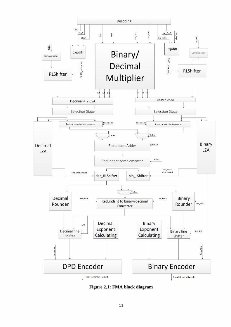
blocks in the FMA design are separate for each format. The top level block diagram of
the FMA is shown in Figure 2.1.
In the next sections we will go through more details about the FMA unit
implementation.
2.3. Decoding the inputs
The FMA supports decimal and binary 64 bits formats, the inputs to the FMA unit
are:
1. Multiplier “OpA” (64 bits)
2. Multiplicand “OpB” (64 bits)
3. Addend “OpC” (64 bits)
4. Binary decimal selection bit “bd” (1 bit)
5. Select operation control signal “selop” (3 bits)
6. Rounding direction “round” (3 bits)
The first three inputs are the FMA input operands, the FMA can work as a multiplier
or adder directly so in these cases the unit takes only OpA and OpB or OpA and OpC.
The bd signal is used to select between binary and decimal operation modes where binary
mode of operation is selected when bd is high and decimal mode is selected otherwise.
The bd signal is used in multiple places in the control path of the FMA to select between
the binary and the decimal results. The selop signal is used to select between the different
operations that the FMA supports, the selop signal decoding is shown in Table 2.1 where
x in the selop value implies don’t care value (i.e. matches 0 or 1). The round signal is
used to define the rounding mode, the supported rounding modes and the corresponding
selection values for the round signal are shown in Table 2.2, where all the IEEE 754-
2008 rounding modes are supported in the FMA in addition to other commonly used
ones. The same decoding for selop and round signals applies for both binary and decimal
operations.
11
Figure 2.1: FMA block diagram
12
Table 2.1: selop signal decoding
selop value Operation Equation
0 x 0 FMA OpAxOpB+OpC
0 x 1 FMS OpAxOpB-OpC
1 0 x Multiplication OpAxOpB
1 1 0 Addition OpA+OpC
1 1 1 Subtraction OpA-OpC
Table 2.2: round signal decoding
round value Rounding mode
000 Round to nearest, Ties to even
001 Round away from zero
010 Round towards positive infinity
011 Round towards negative infinity
100 Round towards zero
101 Round to nearest, Ties away from zero
110 Round to nearest, Ties towards zero
The decoding for the three inputs is done in parallel, the input to the decoding step
is encoded in the IEEE 754-2008 standard encoding either in decimal or binary format.
The decoding step is done to extract the sign, exponent and significand from the encoded
input. Any special values like subnormal in case of binary, zero, NaN or infinity is
detected in this step and a corresponding flag is signaled to be used in the control path of
the FMA remaining steps.
The binary encoding step is simpler than the decimal one. The input operand is
divided into sign, exponent and significand, the only special handling that is done in
binary is to identify if the number is normal or subnormal and add 1 or 0 as the MSB of
the significand accordingly.
In the decimal decoding step the input numbers are in the decimal IEEE encoding
format which is more convenient for the hardware units. The encoding used is the
densely-packed-decimal and the significand is then converted to the BCD 8421 format.
2.4. Multiplication
The significands of the first two inputs are sent to the multiplier after being decoded.
In parallel the exponents are sent to the exponent unit calculation and compared to the
addend exponent. The multiplier unit is shared between the decimal and binary paths
although they have different significand widths where significand width for binary is 53
bits while in decimal the width is 64 bits. The multiplication is done in two steps, the first
step is the partial products generation and the second one is the partial products reduction.

13
The output of the multiplier unit after partial products reduction is three vectors that will
be added to the addend.
2.4.1. Partial products generation
The partial products are generated for both binary and decimal using two separate
units, but the partial products reduction is shared between the two formats. Different radix
values are used for decimal and binary as explained below. Considering the multiplier
and the multiplicand significands as A and B in our explanation going forward.
2.4.1.1. Decimal partial products generation
The SD Radix-5 architecture is used in the decimal multiplication, the partial
products are generated in BCD 8421 format. In SD Radix-5, each multiplier digit is
recoded from the normal digit set where 𝐵𝑖 ∈ {0,1,2,3, … ,9} to the radix-5 encoding 𝐵𝑖 =5 x 𝐵𝑖
𝑈 + 𝐵𝑖𝐿 where the upper digit 𝐵𝑖
𝑈 ∈ {0,1,2} and the lower digit 𝐵𝑖𝐿 ∈ {−2, … ,2}
as shown in Table 2.3. The multiplicand multiples (±𝐴, ±2𝐴, 5𝐴, 10𝐴 ) need to be
generated in BCD-8421 to be ready for the multiplication process. All the positive
multiples are easy decimal multiples that can be obtained without carry propagation and
with few gate delays. For negative multiples needed in the lower partial products, the 9’s
complement is obtained first using two gate delay logic, a (+1) is added at the least
significant digit in the corresponding upper field product to obtain the 10’s complement.
Table 2.3: Decimal digit encoding in Radix-5 format
Digit 𝑩𝒊 𝑩𝒊𝑼 𝑩𝒊
𝑳
0 0 0
1 0 1
2 0 2
3 1 -2
4 1 -1
5 1 0
6 1 1
7 1 2
8 2 -2
9 2 -1
The multiplier digits are used to select from the calculated multiplicand multiples to
generate the partial product, where the upper digit selects from {0,5A,10A} and the lower
digit selects from {0,1A,2A}, the sign bit of the lower digit negates the partial product
selected by the lower digit.
In order to simplify the partial products selection each digit from the upper and lower
digits of the multiplier are represented using multiple selection signals where the upper
digit 𝐵𝑖𝑈 is represented as two signals {𝑦1𝑖
𝑈 , 𝑦2𝑖𝑈} and the lower digit 𝐵𝑖
𝐿 is represented
as 4 signals {𝑦(+2)𝑖𝐿, 𝑦(+1)𝑖
𝐿 , 𝑦(−1)𝑖𝐿 , 𝑦(−2)𝑖
𝐿} in addition to one extra signal for the
sign 𝑦𝑠𝑖. The selection bits truth table is shown in Table 2.4.
14
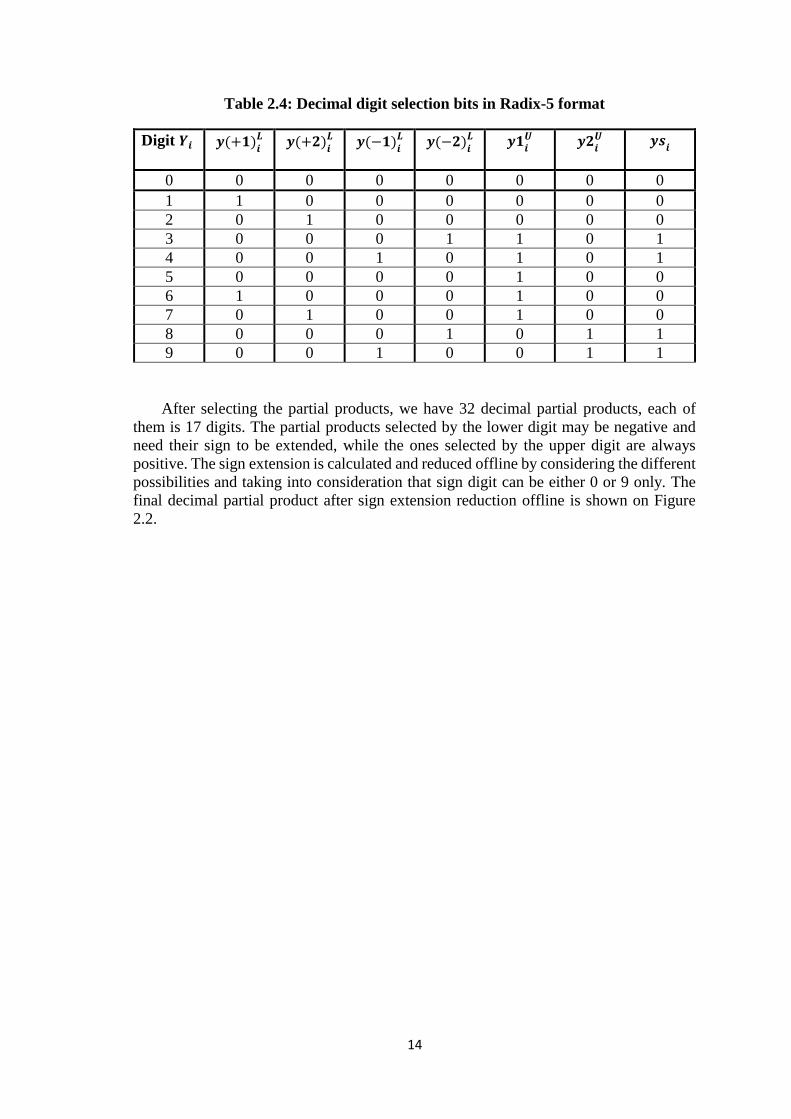
Table 2.4: Decimal digit selection bits in Radix-5 format
Digit 𝒀𝒊 𝒚(+𝟏)𝒊𝑳 𝒚(+𝟐)
𝒊𝑳 𝒚(−𝟏)
𝒊𝑳 𝒚(−𝟐)
𝒊𝑳 𝒚𝟏
𝒊𝑼 𝒚𝟐
𝒊𝑼 𝒚𝒔
𝒊
0 0 0 0 0 0 0 0
1 1 0 0 0 0 0 0
2 0 1 0 0 0 0 0
3 0 0 0 1 1 0 1
4 0 0 1 0 1 0 1
5 0 0 0 0 1 0 0
6 1 0 0 0 1 0 0
7 0 1 0 0 1 0 0
8 0 0 0 1 0 1 1
9 0 0 1 0 0 1 1
After selecting the partial products, we have 32 decimal partial products, each of
them is 17 digits. The partial products selected by the lower digit may be negative and
need their sign to be extended, while the ones selected by the upper digit are always
positive. The sign extension is calculated and reduced offline by considering the different
possibilities and taking into consideration that sign digit can be either 0 or 9 only. The
final decimal partial product after sign extension reduction offline is shown on Figure
2.2.

15
Figure 2.2: Final decimal partial product tree
2.4.1.2. Binary partial products generation
For binary, the SD Radix-4 architecture is used instead. In SD Radix-4 each 4 bits
are decoded together with a carry in from the lower significant 4 bits to produce two
digits and a carry out for the next level. The carry out is calculated directly from the input
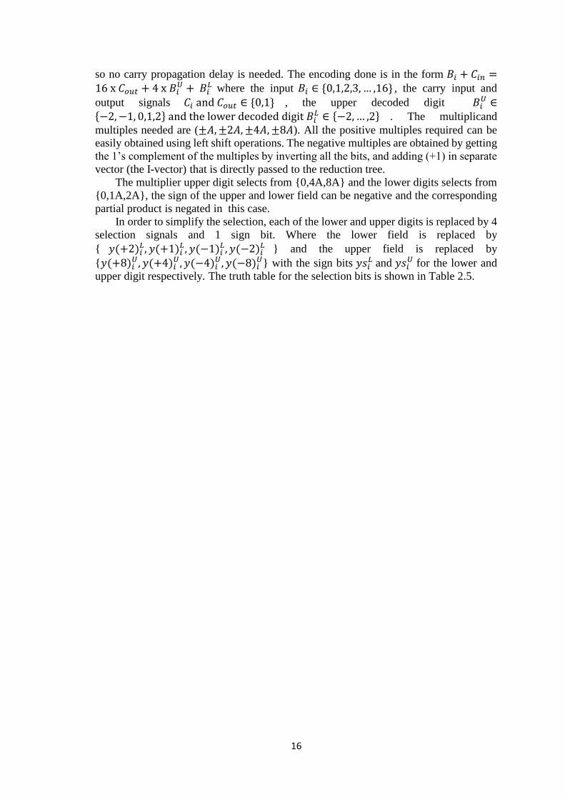
16
so no carry propagation delay is needed. The encoding done is in the form 𝐵𝑖 + 𝐶𝑖𝑛 =16 x 𝐶𝑜𝑢𝑡 + 4 x 𝐵𝑖
𝑈 + 𝐵𝑖𝐿 where the input 𝐵𝑖 ∈ {0,1,2,3, … ,16} , the carry input and
output signals 𝐶𝑖 and 𝐶𝑜𝑢𝑡 ∈ {0,1} , the upper decoded digit 𝐵𝑖𝑈 ∈
{−2, −1, 0,1,2} and the lower decoded digit 𝐵𝑖𝐿 ∈ {−2, … ,2} . The multiplicand
multiples needed are (±𝐴, ±2𝐴, ±4𝐴, ±8𝐴). All the positive multiples required can be
easily obtained using left shift operations. The negative multiples are obtained by getting
the 1’s complement of the multiples by inverting all the bits, and adding (+1) in separate
vector (the I-vector) that is directly passed to the reduction tree.
The multiplier upper digit selects from {0,4A,8A} and the lower digits selects from
{0,1A,2A}, the sign of the upper and lower field can be negative and the corresponding
partial product is negated in this case.
In order to simplify the selection, each of the lower and upper digits is replaced by 4
selection signals and 1 sign bit. Where the lower field is replaced by
{ 𝑦(+2)𝑖𝐿, 𝑦(+1)𝑖
𝐿 , 𝑦(−1)𝑖𝐿 , 𝑦(−2)𝑖
𝐿 } and the upper field is replaced by
{𝑦(+8)𝑖𝑈, 𝑦(+4)𝑖
𝑈, 𝑦(−4)𝑖𝑈, 𝑦(−8)𝑖
𝑈} with the sign bits 𝑦𝑠𝑖𝐿 and 𝑦𝑠𝑖
𝑈 for the lower and
upper digit respectively. The truth table for the selection bits is shown in Table 2.5.

17
Table 2.5: Binary selection bits in Radix-4 format
Y cin 𝒚(𝟏)𝒊𝑳 𝒚(𝟐)
𝒊𝑳 𝒚(−𝟏)
𝒊𝑳 𝒚(−𝟐)
𝒊𝑳 𝒚𝒔
𝒊𝑳 𝒚(𝟒)
𝒊𝑼 𝒚(𝟖)
𝒊𝑼 𝒚(−𝟒)
𝒊𝑼 𝒚(−𝟖)
𝒊𝑼 𝒚𝒔
𝒊𝑼 cout
0 0 0 0 0 0 0 0 0 0 0 0 0
0 1 1 0 0 0 0 0 0 0 0 0 0
1 0 1 0 0 0 0 0 0 0 0 0 0
1 1 0 1 0 0 0 0 0 0 0 0 0
2 0 0 0 0 1 1 1 0 0 0 0 0
2 1 0 0 1 0 1 1 0 0 0 0 0
3 0 0 0 1 0 1 1 0 0 0 0 0
3 1 0 0 0 0 0 1 0 0 0 0 0
4 0 0 0 0 0 0 1 0 0 0 0 0
4 1 1 0 0 0 0 1 0 0 0 0 0
5 0 1 0 0 0 0 1 0 0 0 0 0
5 1 0 1 0 0 0 1 0 0 0 0 0
6 0 0 0 0 1 1 0 1 0 0 0 0
6 1 0 0 1 0 1 0 1 0 0 0 0
7 0 0 0 1 0 1 0 1 0 0 0 0
7 1 0 0 0 0 0 0 1 0 0 0 0
8 0 0 0 0 0 0 0 0 0 1 1 1
8 1 1 0 0 0 0 0 0 0 1 1 1
9 0 1 0 0 0 0 0 0 0 1 1 1
9 1 0 1 0 0 0 0 0 0 1 1 1
10 0 0 0 0 1 1 0 0 1 0 1 1
10 1 0 0 1 0 1 0 0 1 0 1 1
11 0 0 0 0 0 1 0 0 1 0 1 1
11 1 0 0 0 0 0 0 0 1 0 1 1
12 0 0 0 0 0 0 0 0 1 0 1 1
12 1 1 0 0 0 0 0 0 1 0 1 1
13 0 1 0 0 0 0 0 0 1 0 1 1
13 1 0 1 0 0 0 0 0 1 0 1 1
14 0 0 0 0 1 1 0 0 0 0 0 1
14 1 0 0 1 0 1 0 0 0 0 0 1
15 0 0 0 1 0 1 0 0 0 0 0 1
15 1 0 0 0 0 0 0 0 0 0 0 1
The number of bits in case of binary is 53 bits which is extended by 3 zeros on the
left hand side of the number to obtain 56 bits. The 56 bits is divided into 14 groups
resulting in the generation of 28 partial products in addition to the extra I vector. Unlike
the case of decimal, all the 28 partial products can be negative so sign extension is needed
18
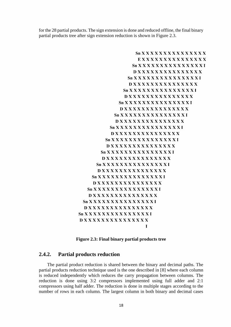
for the 28 partial products. The sign extension is done and reduced offline, the final binary
partial products tree after sign extension reduction is shown in Figure 2.3.
Figure 2.3: Final binary partial products tree
2.4.2. Partial products reduction
The partial product reduction is shared between the binary and decimal paths. The
partial products reduction technique used is the one described in [8] where each column
is reduced independently which reduces the carry propagation between columns. The
reduction is done using 3:2 compressors implemented using full adder and 2:1
compressors using half adder. The reduction is done in multiple stages according to the
number of rows in each column. The largest column in both binary and decimal cases
19
contains 32 digits, this requires 8 stages of reduction to obtain the final summation of the
column in addition to two carry digits. The smallest reduction tree is done for the first
column with only 4 inputs and it takes only 2 stages.
The outputs from the reduction tree are three vectors that will be added to the addend
in a carry save adder (CSA) after that, the CSA adder generates two vectors that will be
applied to the final redundant adder. The binary results output from the reduction tree
can be used directly while the decimal result still needs to be converted from binary back
to BCD format.
2.5. Preparing the addend
In parallel to multiplication, the third operand is prepared for the addition operation.
The exponent of the multiplication operation is done by summing the exponents of the
first two operands and subtracting the IEEE standard defined bias. The calculated
multiplication exponent is compared to the exponent of the third operand to calculate the
shifting amount required to align the operands of the CSA. To avoid adding extra delay
on the multiplication path, the multiplication output will never be shifted and instead the
addend will be shifted right or left according to the exponent difference.
Because the working width is finite number so the shift amount has maximum limit
even if the exponent difference was higher than this limit. The working width differs in
case of binary and decimal, and is selected as small as possible to reduce the area.
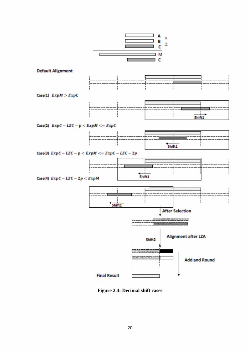
20
Figure 2.4: Decimal shift cases

21
Figure 2.5: Binary shift cases
22
The maximum shift amount is determined by understanding the effect of the shift in
different scenarios. For example if the addend is shifted by very large amount to the left,
this means that the multiplication results does not contribute to the final result except by
the sticky bit. In this case it is enough to shift the addend by the minimum amount that
makes the multiplication result only affects the sticky calculation.
The different shift scenarios for decimal and binary are shown in Figure 2.4 and
Figure 2.5.
2.6. Carry save adder
The CSA adder takes the three outputs of the multiplier as well as the shifted addend,
the CSA does 4:2 compression and produces two vectors to be added in the final
redundant adder. Separate CSA units are used for the binary and the decimal paths.
The effective operation is calculated by considering the signs of all the operands as
well as the original operation. The eop is simply the xor of all the previous 4 signals.
2.7. Leading Zeros anticipation
In parallel to the redundant addition the leading zeros are anticipated from the two
vectors output of the CSA to determine the shift amount required on the summation in
redundant format. The leading zeros detection technique uses an inexact calculation
followed by a correction to obtain the final leading zeros count as in [10].
The LZD result is generated in base 3 format to be used directly on the redundant
format summation before converting back to binary. Leading ones detection is also done
in parallel for the case of effective subtraction.
2.8. Redundant adder
The addition is done on the redundant system to be able to do carry free addition thus
decreasing the delay. The two output vectors from the CSA unit are added in this stage.
The binary and decimal vectors are both converted to the same redundant format to be
able to share the same adder. Each three bits of the binary signal form one redundant
digit, while for the decimal one decimal digit is corresponding to one redundant digit.
The redundant system used operates on the value set [-6,6] encoded in the two’s
complement format instead of the original representation ([0,9] in the case of decimal,
and [0,7] in the case of octal), which does not support a carry-free addition/subtraction.
2.8.1. Conversion from Binary/Decimal to Redundant
The pseudo code for conversion to redundant is shown in Figure 2.6 where:
ITDi = OTDi-1
inputi is the input digit at location i
INTi is the intermediate sum
radix = 10 for decimal, and 8 for octal
OTD, and ITD are the output and input transfer digits respectively

23
if (inputi > 5){
INTi = inputi - radix;
OTDi = 1;
}
else
{
INTi = inputi ;
OTDi = 0;
}
outputi = INTi+ ITDi;
Figure 2.6: Procedure for converting to redundant
The truth table for conversion from decimal to redundant is shown in Table 2.6, and
for binary shown in Table 2.7.
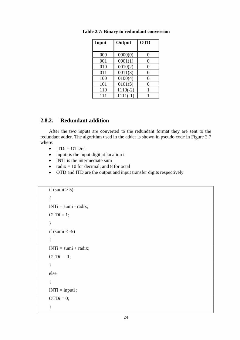
Table 2.6: Decimal to redundant conversion
Input Output OTD
0 0000(0) 0
1 0001(1) 0
2 0010(2) 0
3 0011(3) 0
4 0100(4) 0
5 0101(5) 0
6 1100(-4) 1
7 1101(-3) 1
8 1110(-2) 1
9 1111(-1) 1
24
Table 2.7: Binary to redundant conversion
Input Output OTD
000 0000(0) 0
001 0001(1) 0
010 0010(2) 0
011 0011(3) 0
100 0100(4) 0
101 0101(5) 0
110 1110(-2) 1
111 1111(-1) 1
2.8.2. Redundant addition
After the two inputs are converted to the redundant format they are sent to the
redundant adder. The algorithm used in the adder is shown in pseudo code in Figure 2.7
where:
ITDi = OTDi-1
inputi is the input digit at location i
INTi is the intermediate sum
radix = 10 for decimal, and 8 for octal
OTD and ITD are the output and input transfer digits respectively
if (sumi > 5)
{
INTi = sumi - radix;
OTDi = 1;
}
if (sumi < -5)
{
INTi = sumi + radix;
OTDi = -1;
}
else
{
INTi = inputi ;
OTDi = 0;
}
25
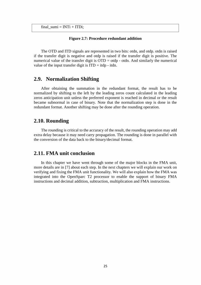
final_sumi = INTi + ITDi;
Figure 2.7: Procedure redundant addition
The OTD and ITD signals are represented in two bits: otdn, and otdp. otdn is raised
if the transfer digit is negative and otdp is raised if the transfer digit is positive. The
numerical value of the transfer digit is OTD = otdp - otdn. And similarly the numerical
value of the input transfer digit is ITD = itdp - itdn.
2.9. Normalization Shifting
After obtaining the summation in the redundant format, the result has to be
normalized by shifting to the left by the leading zeros count calculated in the leading
zeros anticipation unit unless the preferred exponent is reached in decimal or the result
became subnormal in case of binary. Note that the normalization step is done in the
redundant format. Another shifting may be done after the rounding operation.
2.10. Rounding
The rounding is critical to the accuracy of the result, the rounding operation may add
extra delay because it may need carry propagation. The rounding is done in parallel with
the conversion of the data back to the binary/decimal format.
2.11. FMA unit conclusion
In this chapter we have went through some of the major blocks in the FMA unit,
more details are in [7] about each step. In the next chapters we will explain our work on
verifying and fixing the FMA unit functionality. We will also explain how the FMA was
integrated into the OpenSparc T2 processor to enable the support of binary FMA
instructions and decimal addition, subtraction, multiplication and FMA instructions.

26
27
Chapter 3 : FMA unit verification
3.1. FMA unit initial verification
As part of his work, A. Adel has verified the FMA design to work in both binary and
decimal modes [7]. He tested his work using simulation based verification, by applying
large number of test vectors that should cover the different scenarios in the design and
verifying that the output and flags are generated as expected.
For decimal operations verification, the FMA was tested as a full operation as well
as testing the multiplier and adder as separate operations. Large number of test vectors
were applied to hit all the corner cases. The test vectors used were created by A. Ahmed
et al in [11] using constraint based random test vectors generation technique. More than
1.1 million test vectors were used to verify all the decimal operations supported by the
unit. The unit passed all the test vectors.
For binary operations verification, less testing has been done because of the lack of
open source binary floating point test vectors. The unit has been tested in different cases
such as underflow, overflow, zero result, subnormal result, subnormal inputs, massive
right and left shift, normal operation. The unit also passed all the tests and gave correct
results.
3.2. FMA unit extended verification
Before integrating the FMA unit in the OpenSparc T2 processor we wanted to do
more testing and verification to guarantee that the unit is functioning correctly in all
scenarios, especially for the binary unit since it was not fully verified as highlighted by
the author.
3.2.1. FPU verification techniques and challenges
The verification of the floating point units has always been challenging task because
of the large number of test vectors needed to cover all the possible input combinations.
The two techniques that are commonly used in verification of FPUs are formal
verification techniques and simulation based verification techniques.
The verification of any FP operation has at least to cover the combinations of the
following basic scenarios:
1. Different FP numbers types for the operands or the result:
a. Normal
b. Subnormal (in case of BFP) or number cohorts (in case of DFP)
c. NaN
d. Infinity
e. Zero
2. Verify the IEEE flags generation
a. Inexact flag
b. Overflow flag
c. Underflow flag
d. Invalid flag
28
e. Division by zero flag
3. The IEEE rounding modes
a. Rounding to nearest
b. Rounding to zero
c. Rounding to +ve infinity
d. Rounding to –ve infinity
Because there are large number of scenarios to cover, it is hard to calculate how
much of testing is enough for your design. As an example for multiplication, the overflow
can occur due to any of the below reasons:
1. Overflow occurs after adding the exponents because the resultant exponent is
greater than the maximum
2. The resultant exponent just reached the maximum. The overflow is caused by
the resultant of multiplying the mantissa
3. The resultant exponent and mantissa just reached the maximum. The overflow
occurs after rounding
So to verify that overflow detection is working correctly, you will need to have
multiple scenarios that hit the overflow from the three different reasons. Note that with
random test vectors generation it is more likely to hit the overflow due to the first reason.
The likelihood for the second reason is also higher than the third reason which is
considered very corner case and need special handling to generate test vectors to hit it.
3.2.1.1. FPU simulation based verification
The simulation based verification is inefficient in obtaining good verification for the
FPU due to the large input space as explained above. However, some techniques like
constraint random test vectors generation as proposed in [11,12] may help in obtaining
better coverage with less number of test vectors but still cannot guarantee full coverage
or bug free design. The constraint random test vectors generation techniques can easily
generate test vectors to hit the corner cases but the challenge would be in identifying all
the interesting scenarios to cover. We have used the generated test vectors from [12] as
part of our verification for the binary FMA functionality.
3.2.1.2. FPU Formal verification
The formal verification on the other side can guarantee full coverage for the design
and can detect corner cases bugs. The formal verification for FPU can be done by either
theorem proving or by model checking. The theorem proving is done by defining
theorems for the expected design functionality and using mathematical reasoning to
prove it. The model checking is done by defining properties for the design and using
mathematical model to explore the states and prove the properties.
The formal verification techniques are harder than simulation, it is also not reusable
in case of theorem proving since the defined theorems depend on the verified design. The
model checking can also suffer from state explosion if the number of states is very large,
this can be handled by applying the bounded model checking methods, however, no proof
can be obtained in this case.
A lot of research has been done in formal verification targeting the verification of
the hardware implementation of the FPU. The research areas in formal verification for
floating point arithmetic are:
Developing data structures suitable for verifying FPU
o The authors in [13] proposed the use of new data structure that is
developed specifically for the arithmetic operations and has linear
29
increase with the data size. The data structure is called Multiplicative
Power Hybrid Decision Diagrams (*PHDD). This flow was used to
verify the multiplication results before rounding.
Using combined flow of theorem proving and model checking
o In [14] hybrid flow combining both theorem proving and model
checking techniques was proposed, the flow starts by verifying the
main blocks before working on verifying the full design. This flow
managed to detect many bugs both in design and specifications,
however, many of them -according to the authors- can be easily
detected using test vectors simulation. The model checking
mechanism used is called Symbolic trajectory evaluation (STE) and
is based on symbolic simulation.
o In [15] the authors proposed formal verification flow using theorem
proving and model checking techniques without relying on any
specialized representations like the Binary Moment Diagram (BMD).
The proposed flow uses the STE model checking and tries to break
the verification problem into verifying the smaller blocks of the
multiplier.
Theorem proving
o In [16], the authors used automatic theorem proving for verifying the
AMD-K7 processor’s FPU. The proof done was based on a formal
description of the hardware, derived from a C model. The flow was
successful in detecting two flaws in the design.
o In [17] PVS theorem-prover was used in hierarchical approach at the
gate level to verify the implementation of Even-Seidel rounding
algorithm.
o In [18] the theorem proving technique (Coq) was used to verify the
end-around-carry adder which is commonly used in floating point
circuits.
o In [19] Higher Order Logic (HOL) theorem proving has been
proposed, the use of HOL allows for a clear and precise description
of the IEEE standard specification.
o In [20] PVS theorem proving is used at gate level to verify FPU
functionality
Model checking:
o In [21], word level model checking technique was proposed to
overcome the limitation of the symbolic model checking in dealing
with data path verification. The paper also highlights how the new
proposed technique can avoid the Pentium FDIV error.
o In [22] word-level symbolic model checking, *PHDDs, conditional
symbolic simulation as well as a short-circuiting techniques are used
for verifying floating point adders. The flow was applied on FP adder
from University of Michigan and managed to detect many design
bugs.
Equivalence checking
o In [23] formal verification based on BDD- and SAT-based symbolic
simulation is used to compare the FMA design to a high level
description of the same unit written in VHDL.
o Sequential Equivalence Checking is proposed in [24] by comparing
the design to its reference model to easily verify the correctness of

30
the floating point design. In addition to verifying the single
instruction in the design, the paper proposes a method to verify the
processor control path by comparing the result from single
instructions to that of the same instruction but in the middle of other
set of instructions.
As an alternative to the simulation based verification approach used in [7] which
requires the user to use large number of verified test vectors to be able to get good
verification for the design, we have used formal verification tool that depends on model
checking technology. Instead of driving the design with specific stimulus during the
simulation, the formal tool will try to prove or find a counter example for all the
properties defined in the design by exploring all the solution space. This is more efficient
than providing large list of test vectors manually. However, the user has to understand
the system to be able to define the properties. The properties are defined in IEEE
SystemVerilog standard language [25]. During our work we have shown list of properties
that can be tested, we explained how properties can be defined and verified at the block
level as well as the full design level. At the end of this chapter we have developed more
generic approach that can be used to verify the FPU without depending on the internal
design by defining a high level model for the FPU operation. We have proved the
effectiveness of our approach in detecting bugs on the FMA unit. The contributions in
the proposed FPU verification are:
The checker is specified in a standard language with embedded assertions to
verify the different scenarios in the FPU
The checker can be used in formal verification or simulation
The checker is generic and can be used with any floating point unit
3.3. Applying simulation test vectors on the FMA unit
The test vectors generated in [12] for verifying the double precision binary floating
point addition and multiplication are used. The test vectors are covering the three basic
operations: multiplication, addition, and subtraction. Unfortunately no test vectors are
available for the complete FMA operation.
The test vectors have the following fields:
The first operand
The second operand
The rounding direction
The operation type
The expected output
The expected flags
A testbench has been developed to apply the list of test vectors on the FMA design
and compare the FMA output and flags to the expected ones using SVA. Applying sample
of the test vectors showed that the main functionality of the binary FMA is broken as
shown on Table 3.1.

31
Table 3.1: Initial simulation results for the FMA unit
Tested operation # of test
vectors
# of fail # of pass
Multiplication 10 10 0
Add/Subtract 10 10 0
Since simulation is already showing some issues in the design, so applying formal
verification is expected to show similar issues. However, we applied the formal
verification as well to explain how formal verification can be used to detect, fix and verify
bugs.
3.4. Applying design checks on the FMA unit
As a first step in applying the formal verification, the user should review and fix any
design issues that may cause the formal verification tool to report false issues.
We used Questa AutoCheck tool from Mentor Graphics for detecting issues in the
design implementation, Questa AutoCheck tool is a fully-automated tool that leverage
formal technology for detecting design issues such as dead code, floating signals,
multiple driven signals, register stuck at value, Finite State Machine deadlock,
combinatorial loops and many other checks for issues that would cause simulation-
synthesis mismatch or cause a fault in the design operation [26]. The Questa Autocheck
tool automatically apply properties on the different design parts and try formally to prove
them, otherwise design issue is reported.
The tool ran successfully on the design and reported some design issues as shown in
Table 3.2.
Table 3.2: Design issues in the FMA unit
Design check # of times reported
Unused signals 675
Combinational loop in the design 1
Undriven signals 223
Inferred latches 5
Signals with multiple drivers 2
Unreachable block of the code 4
Overflow from arithmetic operations 6
The reported design issues vary in severity, some of the issues like the unused signals
may be not very critical as it may not affect the functionality while other checks like
undriven signals can cause the design to fail.
We started by going through the reported issues and trying to fix them, we will show
some examples for the different issues reported by the tool and how we were able to fix
them.

32
As an example for the undriven signals issue, the tool has reported that the two
signals bin_signM and bin_signIR have no drivers. Going through the RTL
implementation of the FMA, I found that those signals are used as inputs to
“RoundingInf” module which is responsible for deciding whether the result is infinity or
not. This issue is fixed by adding the missing assignment for bin_signM and bin_signIR
to be driven the multiplication sign expression and the intermediate sign respectively as
shown in Figure 3.1. The other 221 undriven signals reported by the tool are not critical
because they are not driving any logic, the design was modified to remove the signals to
fix the issue.
// Adding missing assignment for binary sign signals
assign bin_signM = bin_signA ^ bin_signB;
assign bin_signIR = bin_sign;
Figure 3.1: Fixing undriven signal issue
The inferred latches issue was also unexpected in the design since the design is
totally combinational. The latches are inferred due to missing branch in the case
statements as shown in Figure 3.2. This issue is fixed by adding default branch in the
case statement as shown in Figure 3.3.
// Wrong coding style causing latch to be inferred
always@(*)
begin
case({bin_norm_shiftamnt[0],fine_shift})
3'b000: val1 = 13'b0000000000000;
3'b001: val1 = 13'b1111111111111;
3'b010: val1 = 13'b1111111111110;
3'b100: val1 = 13'b1111111111101;
3'b101: val1 = 13'b1111111111100;
3'b110: val1 = 13'b1111111111011;
endcase
end
Figure 3.2: Latch inferred due to wrong coding style
// Fixing the case statement to not infer a latch
always@(*)

33
begin
case({bin_norm_shiftamnt[0],fine_shift})
3'b000: val1 = 13'b0000000000000;
3'b001: val1 = 13'b1111111111111;
3'b010: val1 = 13'b1111111111110;
3'b100: val1 = 13'b1111111111101;
3'b101: val1 = 13'b1111111111100;
3'b110: val1 = 13'b1111111111011;
// Adding default statement
default: val1 = 13'bxxxxxxxxxxxxx;
endcase
end
Figure 3.3: Fixing the coding style to avoid inferring latch in the design
The tool reports one combinational loop in the design, this issue may cause glitches
and other wrong functionalities in the design. This issue was identified in the binary
exponent difference calculation circuit where the subnormal was used to calculate the
correct exponent value, while the calculated exponent value was used to calculate the
subnormal signal as shown in Figure 3.4. This issue was fixed by removing the
combinational loop from the assignment and adding the correct conditions to detect the
subnormal value as shown in Figure 3.5.
// subnormalM signal used to calculate expM
assign expM = (subnormalM) ? expMisn[11:0] : expMi[11:0];
// expM signal used to calculate subnormalM
assign subnormalM = ~expMi[13] | ~(|expM);
Figure 3.4: Combinational loop issue in the design
// Fixed the assignment to not depend on expM signal
assign subnormalM = ~expMi[13] | ~(|expMi);
Figure 3.5: Fixing the combinational loop issue
The signals with multiple drivers issue although can cause mismatches in the results
but in this design the signal was never used so this issue is ignored.

34
The unreachable block in the code is an issue because it means that the block of the
code can never be hit and this in most of the scenarios is an unintended behavior. As an
example for the unreachable code issue, the tool detects uncoverable scenarios in the
binary leading zero detection unit as shown in Figure 3.6. By tracing the valid signal I
found it always has value 1 because of the constants used while instantiating this module
in the design. The code has been optimized by replacing the case statement with simple
assignment as shown in Figure 3.7.
// valid signal is always 1
assign sel = {valid,cin};
always@(*)
begin
case(sel)
// Never reached this branch
2'b00: LZC = 9'b000000000; // all p's
// Never reached this branch
2'b01: LZC = 9'b100101010;//all p's and cin
default: LZC = LZC3;
Figure 3.6: Unreachable block of code issue
// Case statement is replaced by simple assignment
always@(*)
LZC = LZC3;
Figure 3.7: Optimizing the design by removing the unreachable code block
The last type of design issues that we debugged in the FMA RTL code is the
overflow issue that occurs in the arithmetic operations. This issue occurs when the output
of the arithmetic operation requires more bits than the available bits at the RHS of the
assignment. All the instances of this issue where verified to be expected and acceptable.
After fixing all the above issues, we have rerun the tool again to verify that the issues
are no longer reported. The tool reports that the previously reported issues were addressed
correctly. However, a new issue has appeared because of our fix for the latch inferred
issue. In our fix we added a default branch to the case statement with X assignment
because we didn’t expect that this branch to be ever taken. The AutoCheck tool reports a
new issue that this X assignment is reachable in some scenarios so the case statement
shown in Figure 3.3 has to be reviewed again. The scenario that causes the X assignment
is when fine_shift signal is equal to 3, this scenario is not handled in the case statement
and it appears to be reachable value. The design module that is showing this issue is the
one used to calculate the final exponent of the binary result, it is also the module that

35
signals the overflow flag. The module has three inputs which are the resultant exponent
before normalization, and two signals to specify the shift amount for the normalization.
The module uses three signals val1, val2, and val3 to calculate the value to be subtracted
from the exponent to get the final normalized exponent. The case statements that
calculates val1, val2, and val3 has been updated to handle all the scenarios to avoid hitting
the default branch as shown in Figure 3.8.
// The missing conditions have been added to the case statement
always@(*)
begin
case({bin_norm_shiftamnt[0],fine_shift})
3'b000: val1 = 13'b0000000000000;
3'b001: val1 = 13'b1111111111111;
3'b010: val1 = 13'b1111111111110;
3'b011: val1 = 13'b1111111111101;
3'b100: val1 = 13'b1111111111100;
3'b101: val1 = 13'b1111111111001;
3'b110: val1 = 13'b1111111111010;
3'b111: val1 = 13'b1111111111001;
endcase
end
Figure 3.8: Fixing the missing conditions in the case statement
3.5. Formally verifying FMA functionality
3.5.1. Testing the overall FMA functionality
3.5.1.1. Formal verification tool
After fixing the design issues, we started working on verifying the design
functionality. In this step in our verification flow we applied Formal verification method
with Assertion Based Verification (ABV) to test, verify and debug the FMA unit. We
used Questa Formal tool from Mentor Graphics for the formal verification work
described in this section [27]. Questa Formal tool is based on model checking technology
and it automatically verifies that the design behavior matches the specification by
exploring all the possible design states in breadth-first manner.

36
3.5.1.2. SystemVerilog language
The design specification is written in IEEE standard SystemVerilog [25] assertions
construct. The SystemVerilog is an IEEE standard unified language that is used for both
hardware design and hardware verification. The SystemVerilog Assertions (SVA) are
used to describe the expected behavior of the system, simulation and formal tools can be
used to verify that the design behavior is matching the expected behavior. The SVA used
can vary from describing very simple properties such as onehot to specifying a complete
sequence that may take few cycles to complete.
We have used the following three types of properties supported in SystemVerilog:
Assertions: used to verify that the design behavior is matching the property
defined in the assertion. The assertions are applicable in both simulation and
formal verification with the basic difference that in simulation the user is
responsible to drive the design with values that activate and exercise the
assertions completely while this is automatically handled in formal
verification. There are two types of assertions specified in the design, we
have used both types in different parts of our verification as explained the
next sections:
o Concurrent assertions: The concurrent assertions are evaluated all the
time during simulation or formal verification run. This is useful to
define properties that should always be valid in the design.
o Immediate assertions: The immediate assertions are evaluated only
when the block including the assertion is evaluated. This is useful to
enable the assertion only if some condition is met.
Assumptions: this is similar to the syntax of the concurrent assertions. The
assumptions are applicable only in formal verification run and are used to
constrain the formal tool with specific properties.
Coverage statements: this is similar to the syntax of the concurrent assertions.
The coverage statements can be used in simulation or formal verification
runs. In simulation run, the coverage statement is used to check if certain
property is covered by the testing or not. In formal run, since there is no
testbench to drive the design, the coverage statement is used to check if
certain property can be covered or not.
3.5.1.3. Defining system properties
Our testing is divided into two parts, the first part is targeting the binary operations
while the second part is targeting the decimal operations. The reasons that we wanted to
verify each mode separately are:
1. The binary and decimal operations are using some common resources but most
of the work done in the operations are in different units
2. It is easier to debug issues when separating the two modes
3. Make sure that we cover all possibilities in each mode in our testing
4. The checks that we apply can be different in binary than in decimal
As a first step in our Formal verification flow we wanted to make sure that the output
signals can have all the expected results. We did an essential check that no bits are stuck
at 0 or stuck at 1, this type of issues is common due to wrong connections in the design.
We used SystemVerilog (SV) coverage statements to specify the cover items that we
want to check. We added two coverage statements for each bit, the first directive is used

37
to test that the bit can be assigned 0 value while the other directive is checking that the
bit can be assigned 1 value. The design has two outputs OpR (64 bits) and flags (4 bits)
so we added 136 cover directives and used Formal tool to check that all of them are
coverable. We applied the same test for binary and decimal and we got all the cover
directives covered in both cases. Figure 3.9 shows example for the cover directives that
we used for the flags.
// Using generate statement to loop through the 4 bits of the flags output
generate
for (i=0; i<4; i++)
begin
// Check that flags[i] can take value 0
cover property (@(posedge clock) (flags[i] == 1'b0));
// Check that flags[i] can take value 1
cover property (@(posedge clock) (flags[i] == 1'b1));
end
endgenerate
Figure 3.9: Specifying cover directives to verify that the output signals can toggle
After checking that the output signals can toggle with no issues, we proceed with our
testing by adding some assertions to verify some basic functionality of the design.
The special values that can be generated from the FMA unit are:
1. Zero
2. Subnormal
3. Infinity
4. qNaN
We added cover items to make sure that all the above values are reachable. We added
extra assertion to verify that the output is never sNaN since this value isn’t expected at
the output of the FMA operation. The assertions and cover properties that we used to
verify this behavior are shown in Figure 3.10. Note that the values compared in case of
binary should be different from the case of decimal because of how the special values are
specified in the standard for each format.
// Check for the final result of the FMA unit in case of binary operations, the bd
signal is used to disable the assertion in case of decimal operation
// Assert that the sNaN value should never appear at the output of the FMA
assert property (@(posedge clock) (bd -> (!OpR[51] && OpR[62:52] == 11'h7ff
&& OpR[51:0] != 0))); // snan
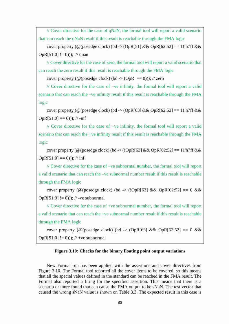
38
// Cover directive for the case of qNaN, the formal tool will report a valid scenario
that can reach the qNaN result if this result is reachable through the FMA logic
cover property (@(posedge clock) (bd -> (OpR[51] && OpR[62:52] == 11'h7ff &&
OpR[51:0] != 0))); // qnan
// Cover directive for the case of zero, the formal tool will report a valid scenario that
can reach the zero result if this result is reachable through the FMA logic
cover property (@(posedge clock) (bd -> (OpR == 0))); // zero
// Cover directive for the case of –ve infinity, the formal tool will report a valid
scenario that can reach the –ve infinity result if this result is reachable through the FMA
logic
cover property (@(posedge clock) (bd -> (OpR[63] && OpR[62:52] == 11'h7ff &&
OpR[51:0] == 0))); // -inf
// Cover directive for the case of +ve infinity, the formal tool will report a valid
scenario that can reach the +ve infinity result if this result is reachable through the FMA
logic
cover property (@(posedge clock) (bd -> (!OpR[63] && OpR[62:52] == 11'h7ff &&
OpR[51:0] == 0))); // inf
// Cover directive for the case of –ve subnormal number, the formal tool will report
a valid scenario that can reach the –ve subnormal number result if this result is reachable
through the FMA logic
cover property (@(posedge clock) (bd -> (!OpR[63] && OpR[62:52] == 0 &&
OpR[51:0] != 0))); // -ve subnormal
// Cover directive for the case of +ve subnormal number, the formal tool will report
a valid scenario that can reach the +ve subnormal number result if this result is reachable
through the FMA logic
cover property (@(posedge clock) (bd -> (OpR[63] && OpR[62:52] == 0 &&
OpR[51:0] != 0))); // +ve subnormal
Figure 3.10: Checks for the binary floating point output variations
New Formal run has been applied with the assertions and cover directives from
Figure 3.10. The Formal tool reported all the cover items to be covered, so this means
that all the special values defined in the standard can be reached in the FMA result. The
Formal also reported a firing for the specified assertion. This means that there is a
scenario or more found that can cause the FMA output to be sNaN. The test vector that
caused the wrong sNaN value is shown on Table 3.3. The expected result in this case is
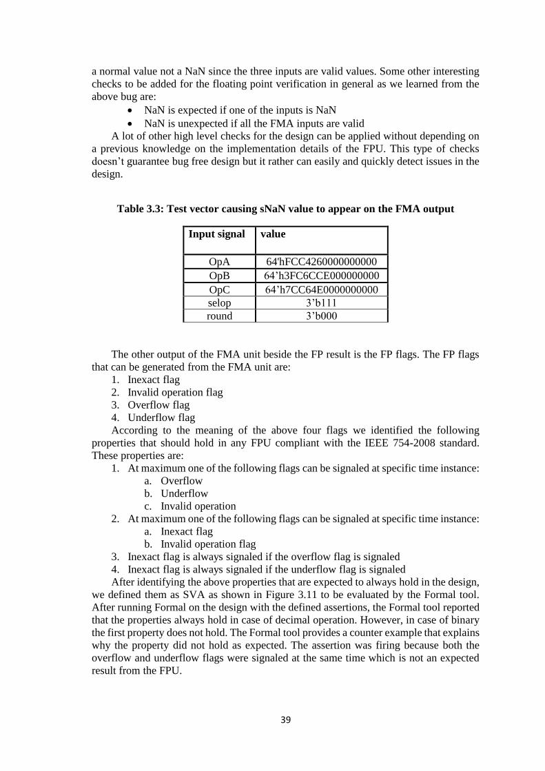
39
a normal value not a NaN since the three inputs are valid values. Some other interesting
checks to be added for the floating point verification in general as we learned from the
above bug are:
NaN is expected if one of the inputs is NaN
NaN is unexpected if all the FMA inputs are valid
A lot of other high level checks for the design can be applied without depending on
a previous knowledge on the implementation details of the FPU. This type of checks
doesn’t guarantee bug free design but it rather can easily and quickly detect issues in the
design.
Table 3.3: Test vector causing sNaN value to appear on the FMA output
Input signal value
OpA 64'hFCC4260000000000
OpB 64’h3FC6CCE000000000
OpC 64’h7CC64E0000000000
selop 3’b111
round 3’b000
The other output of the FMA unit beside the FP result is the FP flags. The FP flags
that can be generated from the FMA unit are:
1. Inexact flag
2. Invalid operation flag
3. Overflow flag
4. Underflow flag
According to the meaning of the above four flags we identified the following
properties that should hold in any FPU compliant with the IEEE 754-2008 standard.
These properties are:
1. At maximum one of the following flags can be signaled at specific time instance:
a. Overflow
b. Underflow
c. Invalid operation
2. At maximum one of the following flags can be signaled at specific time instance:
a. Inexact flag
b. Invalid operation flag
3. Inexact flag is always signaled if the overflow flag is signaled
4. Inexact flag is always signaled if the underflow flag is signaled
After identifying the above properties that are expected to always hold in the design,
we defined them as SVA as shown in Figure 3.11 to be evaluated by the Formal tool.
After running Formal on the design with the defined assertions, the Formal tool reported
that the properties always hold in case of decimal operation. However, in case of binary
the first property does not hold. The Formal tool provides a counter example that explains
why the property did not hold as expected. The assertion was firing because both the
overflow and underflow flags were signaled at the same time which is not an expected
result from the FPU.
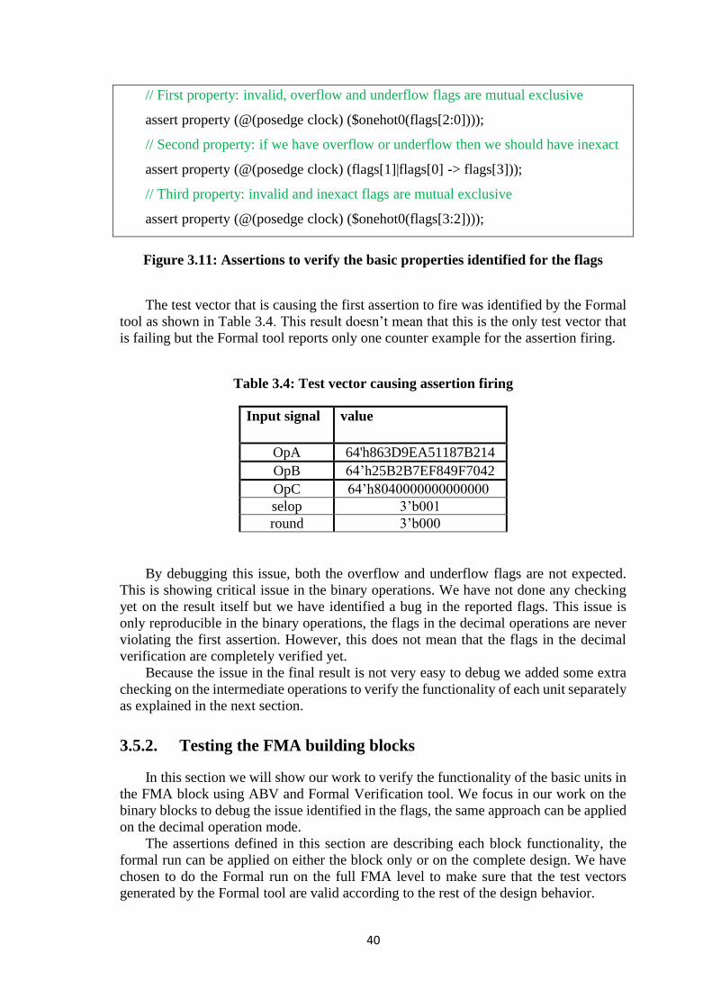
40
// First property: invalid, overflow and underflow flags are mutual exclusive
assert property (@(posedge clock) ($onehot0(flags[2:0])));
// Second property: if we have overflow or underflow then we should have inexact
assert property (@(posedge clock) (flags[1]|flags[0] -> flags[3]));
// Third property: invalid and inexact flags are mutual exclusive
assert property (@(posedge clock) ($onehot0(flags[3:2])));
Figure 3.11: Assertions to verify the basic properties identified for the flags
The test vector that is causing the first assertion to fire was identified by the Formal
tool as shown in Table 3.4. This result doesn’t mean that this is the only test vector that
is failing but the Formal tool reports only one counter example for the assertion firing.
Table 3.4: Test vector causing assertion firing
Input signal value
OpA 64'h863D9EA51187B214
OpB 64’h25B2B7EF849F7042
OpC 64’h 8040000000000000
selop 3’b001
round 3’b000
By debugging this issue, both the overflow and underflow flags are not expected.
This is showing critical issue in the binary operations. We have not done any checking
yet on the result itself but we have identified a bug in the reported flags. This issue is
only reproducible in the binary operations, the flags in the decimal operations are never
violating the first assertion. However, this does not mean that the flags in the decimal
verification are completely verified yet.
Because the issue in the final result is not very easy to debug we added some extra
checking on the intermediate operations to verify the functionality of each unit separately
as explained in the next section.
3.5.2. Testing the FMA building blocks
In this section we will show our work to verify the functionality of the basic units in
the FMA block using ABV and Formal Verification tool. We focus in our work on the
binary blocks to debug the issue identified in the flags, the same approach can be applied
on the decimal operation mode.
The assertions defined in this section are describing each block functionality, the
formal run can be applied on either the block only or on the complete design. We have
chosen to do the Formal run on the full FMA level to make sure that the test vectors
generated by the Formal tool are valid according to the rest of the design behavior.

41
3.5.2.1. Verifying the binary carry save adder (CSA)
We have applied assertions to verify the functionality of this important block.
Although the block implementation is complex but the end result can be simply specified
as a property. The module has four inputs (A,B,C, and D) and two outputs (R0 and R1).
The two outputs are the sum and carry of the addition of the four inputs, therefore we
applied simple assertion as shown in Figure 3.12 to verify that the output of the adder is
correct. Note that $global_clock is a keyword in the SV standard, it is used because the
module does not have clock signals to be used in evaluating the assertion. The
$global_clock in formal verification is considered to be the primary system clock.
// The property can be written as (R0 + R1) === (A + B + C + D), however, we found
that this style is simpler for the formal tool
assert property (@($global_clock) (R0) === (A + B + C + D - R1));
Figure 3.12: Assertions to verify the binary CSA block
Using the assertion in Figure 3.12 we verified that the whole functionality of the
CSA block is correct without getting into the details of the implementations of the CSA
block.
3.5.2.2. Debugging the final binary exponent calculation unit
The binary exponent calculation unit is responsible for generating the final exponent
result and the overflow flag. The inputs to this unit are the exponent before normalization
and the normalization shift amount. The normalization shift amount used in this module
is provided in base 3 format to help in optimizing the normalization shift in redundant
format as explained in Chapter 2. Therefore the module is responsible for two functions:
convert the shift amount to binary and calculate the final exponent after subtracting the
shift amount. To verify the module functionality we have created a small model to the
expected results and used assertion statement to verify the actual behavior matches the
expected behavior. In our model, the base 3 to binary conversion is done on high level
description as shown in Figure 3.13 and is subtracted from the input exponent to calculate
the final exponent of the FMA.
// The assertion used is showing the relation between actual output of the unit exp_Rf
and the expected output according to the input values.
// Using extra signal to make sure we compare same number of bits in the assertion
wire [11:0] expected_result;
assign expected_result = expR - (fine_shift + (3*bin_norm_shiftamnt[1:0]) +
(9*bin_norm_shiftamnt[3:2]) + (27*bin_norm_shiftamnt[5:4]) +
(81*bin_norm_shiftamnt[6]));

42
// Assert that the expected output matches the actual output
assert property (@($global_clock) (exp_Rf === expected_result[10:0]));
Figure 3.13: Assertion used to verify the final exponent calculation unit
After applying the assertion in the Formal run, the Formal tool is showing assertion
firing for the property defined in this module. The reported counter example is
highlighting issue in how the final exponent is calculated and correspondingly the
overflow flag.
The counter example identified by the tool is shown in Table 3.5.
Table 3.5: Test vector causing wrong flags values
Input/output signal Value in decimal
expR 1994
fine_shift 0
bin_norm_shiftamnt 24
exp_Rf 1898
Expected exp_Rf 1949
The expected exp_Rf although not reached in this scenario but is also not valid
according to the design. Therefore the counter example highlights two issues:
The input to the exponent calculation module is wrong
The conversion from base 3 to binary is done wrongly inside the module
We have identified many issues in the way the conversion from base 3 to binary was
done, we have completely rewrote the conversion. We replaced the use of three lookup
tables (LUT) followed by 2 full adder levels by one bigger LUT followed by one level
of half adders. The values for the LUT have been generated using a Perl script that mimic
the functionality of base 3 to binary conversion.
After fixing the issue we wanted to verify that the issue is fixed in the same exact
scenario that was showing the firing and also in any other scenario. To verify the fix on
the same exact scenario we used another feature of the SVA language which is the
assumption directive. The assumption directive constrains the Formal tool to follow the
property defined in the assumption. We used this feature to make the Formal tool go
through the same scenario and verify that the issue is now fixed. The assumption used is
shown in Figure 3.14.
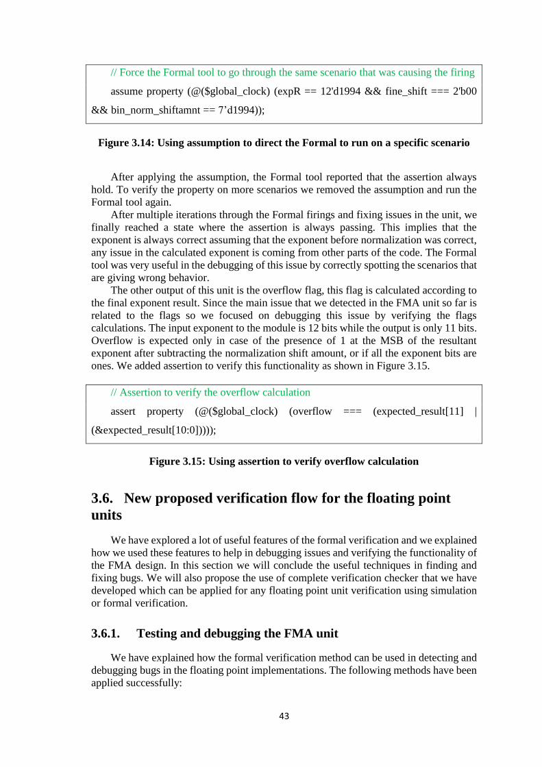
43
// Force the Formal tool to go through the same scenario that was causing the firing
assume property (@($global_clock) (expR == 12'd1994 && fine_shift === 2'b00
&& bin_norm_shiftamnt == 7’d1994));
Figure 3.14: Using assumption to direct the Formal to run on a specific scenario
After applying the assumption, the Formal tool reported that the assertion always
hold. To verify the property on more scenarios we removed the assumption and run the
Formal tool again.
After multiple iterations through the Formal firings and fixing issues in the unit, we
finally reached a state where the assertion is always passing. This implies that the
exponent is always correct assuming that the exponent before normalization was correct,
any issue in the calculated exponent is coming from other parts of the code. The Formal
tool was very useful in the debugging of this issue by correctly spotting the scenarios that
are giving wrong behavior.
The other output of this unit is the overflow flag, this flag is calculated according to
the final exponent result. Since the main issue that we detected in the FMA unit so far is
related to the flags so we focused on debugging this issue by verifying the flags
calculations. The input exponent to the module is 12 bits while the output is only 11 bits.
Overflow is expected only in case of the presence of 1 at the MSB of the resultant
exponent after subtracting the normalization shift amount, or if all the exponent bits are
ones. We added assertion to verify this functionality as shown in Figure 3.15.
// Assertion to verify the overflow calculation
assert property (@($global_clock) (overflow === (expected_result[11] |
(&expected_result[10:0]))));
Figure 3.15: Using assertion to verify overflow calculation
3.6. New proposed verification flow for the floating point
units
We have explored a lot of useful features of the formal verification and we explained
how we used these features to help in debugging issues and verifying the functionality of
the FMA design. In this section we will conclude the useful techniques in finding and
fixing bugs. We will also propose the use of complete verification checker that we have
developed which can be applied for any floating point unit verification using simulation
or formal verification.
3.6.1. Testing and debugging the FMA unit
We have explained how the formal verification method can be used in detecting and
debugging bugs in the floating point implementations. The following methods have been
applied successfully:

44
1. Detecting and fixing any design issues that may cause unexpected behavior, we
have identified many bugs using this approach and handled them.
2. Sanity check to make sure that the FMA outputs can reach all the expected paths
without verifying if the final result is correct or not. In this step we have covered
the following checks:
a. Added checks that the output and flags aren’t stuck at 0 or 1
b. Added checks that the relation between the flags is correct, we have
identified critical issue in the binary calculations for the overflow and
underflow flags
c. Added checks that all the possible special values can be reached from the
FMA logic, again we have identified an issue in the binary calculations
where the sNaN is signaled in some scenarios. This result is not expected
at the output of the FMA operation.
3. Verifying the functionality of the building blocks of the FMA using assertion to
describe the expected output of each block. The Formal run is used to verify the
functionality of each block but instead of running on the block level directly we
decided to run Formal on the full design even when debugging functionality of
blocks, this is done for three reasons:
a. The Formal when run on the full design will only apply the inputs that
are valid in the full design so saves time in debugging unreachable states
b. When debugging you can have full visibility of the behavior of the full
design, this helps in identifying the root cause of the issues faster
c. Running Formal on the top level is also useful if you want to debug the
functionality of multiple blocks in one formal run
3.6.2. Verifying the overall functionality of the FMA unit as a black
box testing
In this section we proposed new verification checker for the validation of floating
point units. The flow is based on formal verification or simulation where the design inputs
(the two operands and the rounding mode) and outputs (the final results and flags) are
provided to the checker to verify that the result is correct. This flow is a black box testing
that is done on the interface signals of the FPU, therefore this approach is highly generic
and can be adapted for any FPU verification.
The checker is connected to the FPU inputs and outputs as shown in Figure 3.16, the
checker can be used in either simulation or formal verification. During the simulation or
formal run the checker will work on verifying that the FPU is working correctly using
the embedded assertions.

45
Figure 3.16: FPU verification checker
We have developed the checker model for BFP multiplication operation, the same
concepts can be used to develop checkers for the other FP operations. The checker
supports both single and double precision formats.
The checker is developed in SV, the main block of code in the checker that calculates
the expected result and flags is about 150 lines of code while the full checker with all the
assertions and IEEE format handling is written in less than 300 lines of code. The
multiplier result evaluation in the checker is written in simple Verilog and with high level
description of operations, therefore it can be easily traced and reviewed.
The checker handles all the special values specified in the standard and verifies the
flags as well as the result.
As a proof of concept for this flow we applied it on the binary multiplier path of the
FMA. The same approach can be applied on the addition and the FMA operations, it is
also applicable for the decimal operations.
The benefit for this approach is that once we get the model built and verified it can
be applied directly on any other unit that has the same functionality since it has no
dependency at all on the implementation details of the unit.
The checker can also be tuned to test only specific ranges either in input or output
by using assumption to constrain the formal run.
Applying the formal verification on the design with the verification checker can
detect all the issues in the design without the need to drive the run with test vectors. The
formal tool is designed to try to find a legal scenario that hits the immediate assertions in
the checker, the test vector generated by the Formal tool will take into consideration all
the conditions specified in the model to reach the assertion. The formal tool will also try

46
to find a scenario that makes the assertion fire so here we are utilizing the formal tool to
automatically explore all the possible values that match the checker conditions and will
check automatically if any of them can cause the assertion to fire.
The checker flowchart is shown in Figure 3.17, the checker takes the two operands
and calculate the expected result and flags and compare them to the actual results. The
first step in the checker flow is decoding the inputs to extract the sign, exponent and
significand of the two operands, the second step is detecting the special values in the
inputs (zero, nan, infinity) because the presence of any of them implies that the output is
already known without the need for extra calculations. If special value is detected at the
input the corresponding output and flags and generated and are directly compared to the
actual output and flags.
If no special values is found in the input operands then we will start calculating the
intermediate result. However, extra step is done to normalize the subnormal numbers to
simplify the calculations after that. After calculating the intermediate results, the checker
will go through one of the following three branches to calculate the final result:
Subnormal result
Overflow in the result
Normal result
In the three above cases rounding is done to calculate the final result and flags. We
have added immediate assertions in each of the branches to verify the result if the branch
is used.
The assertions used in each branch are duplicated for each rounding mode, so the
overall number of assertions used in the checker is 120 assertions (4 rounding modes * 5
for the value and the 4 flags * 6 branches in the code: input NaN, input zero, input infinity,
output subnormal, output has overflow, normal output). This approach allow us to verify
the 120 scenarios in one run.
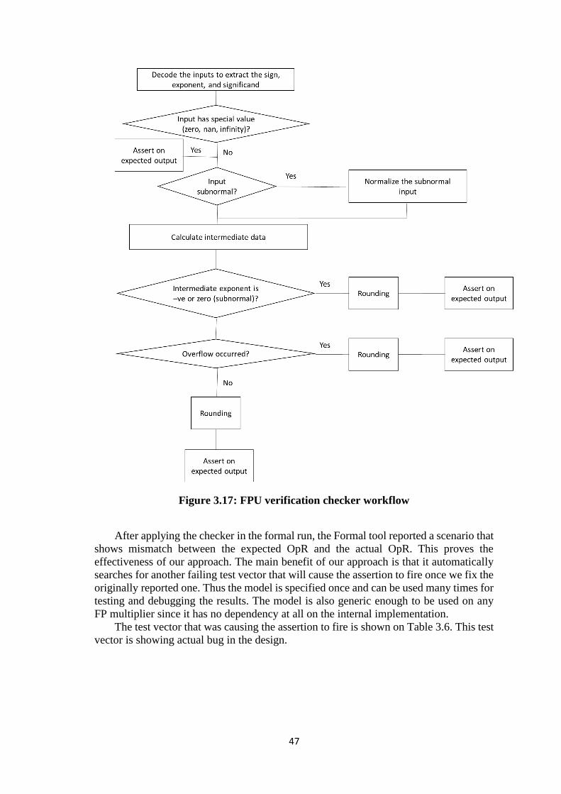
47
Figure 3.17: FPU verification checker workflow
After applying the checker in the formal run, the Formal tool reported a scenario that
shows mismatch between the expected OpR and the actual OpR. This proves the
effectiveness of our approach. The main benefit of our approach is that it automatically
searches for another failing test vector that will cause the assertion to fire once we fix the
originally reported one. Thus the model is specified once and can be used many times for
testing and debugging the results. The model is also generic enough to be used on any
FP multiplier since it has no dependency at all on the internal implementation.
The test vector that was causing the assertion to fire is shown on Table 3.6. This test
vector is showing actual bug in the design.

48
Table 3.6: Test vector causing wrong unexpected FP result
Input/output signal Value
OpA 64’h63cf000000000000
OpB 64’h1b4cf02000000000
selop 3’b100
round 3’b100
OpR 64'h392fce044f800000
Expected OpR 64'h3f2c089f00000000
3.7. Fixing FMA design functionality
As explained in this chapter we have used combination of simulation and formal
verification techniques to verify the binary FMA functionality. We have detected a large
number of bugs and were able to fix many of them. Here is a list of the main blocks that
have been fixed during our work:
1. The decoding of the operands were done wrongly in case of zero. This has
been fixed and verified.
2. The final result encoding was fixed to handle the subnormal result correctly
and handle scenario where result reached the maximum non-infinity value.
3. Binary to base 3 converter: This block is used to convert the exponent from
binary to base 3 format. This functionality is needed to be able to compare the
exponent with the shift amount (which is calculated in base 3 format) to avoid
exceeding the maximum left shift amount that will cause underflow
otherwise. The module in different scenarios was calculating the maximum
shift amount wrongly causing wrong detection of underflow.
4. Base 3 to binary converter: This block is used to convert the shift amount
from base 3 format to binary format. This functionality is needed to convert
the shift amount (in base 3) to binary value than can be subtracted from the
exponent. The module in many cases was doing the conversion wrongly
causing wrong overflow flag and wrong exponent.
5. Binary exponent difference calculation: This module is responsible for
calculating the multiplier exponent and comparing it to the exponent of the
third operand to calculate the shift amount needed for adder alignment. All
the outputs of this module were wrong and have been fixed, these outputs are:
the subnormal detection of the multiplier output, the exponent difference
between the multiplier and the third operand, and the shift direction (right or
left).
6. The handling of multiplier and addition standalone operations were broken
for binary FMA path
7. Fixed the underflow flag generation

49
3.8. Re-verifying the design
We applied simulation tests after fixing the above issues in addition to other issues
mentioned previously in this chapter and some other minor fixes. The testing has been
done using one million test vectors for binary floating point multiplication. The FMA
successfully generated correct result and flags for all the test vectors. Fixing the floating
point addition support is still in progress, as some of the test vectors are still failing.
We have also applied the floating point multiplier checker that we developed after
fixing all the issues detected by the simulation. The checker when run using formal tool
was able to detect some hidden issues that was missed in the simulation testvectors.
The two main bugs that were missed by the simulation and detected by formal are
shown in Table 3.7 and Table 3.8. These scenario were easily detected by formal in about
90 seconds.
Table 3.7: Test vector causing wrong FP multiplier result
Input/output signal Value
OpA 64’h6ffde7cc83f1d2c2
OpB 64’h000a1af963b080a3
selop 3’b100
round 3’b100
OpR 64'h3002e34aa08079bc
Expected OpR 64'h3012e34aa08079bc
Table 3.8: Test vector causing wrong FP multiplier result
Input/output signal Value
OpA 64’h20957dcb4bbaebe7
OpB 64’h07629cc14bf8523e
selop 3’b100
round 3’b100
OpR 64'h7fefffffffffffff
Expected OpR 64'h000000000000000
3.9. Verifying other FP multipliers using our developed
checker
We have applied our checker to verify the BFP multiplier of the OpenSparc T2
design. We have applied our verification on both single precision and double precision
since both are supported in OpenSparc T2 and in our checker.
50
The checker successfully reported that the subnormal support is broken either at the
inputs or the output. We referred to the documentation and found that this limitation is
already mentioned. This is considered another proof of concept of the approach and how
it can be applied on different real designs to detect any hidden bugs.
The differences between the OpenSparc T2 multiplier and the FMA multiplier from
verification points of view are:
OpenSparc T2 multiplier is pipelined
The FMA is a standalone FPU while the OpenSparc T2 FPU is tightly
integrated inside the processor
Because of the above differences and since we are interested in verifying one
instruction at a time we have added support for two new features in the checker:
The Formal is forced to evaluate the results with breadth-first manner, since
the depth search has been disabled by the use of assumption that the checker
input is stable (using SVA $stable() task)
An enable signal can be passed to the checker to enable the assertion only
when data is ready
The verification of the OpenSparc T2 FP multiplier has other challenge also to set
the correct sequence that enable the multiplication pipeline. We have used formal with
coverage statement to explore the required setup to do the multiplication, we have then
forced the formal to use this setup when running with the checker.
3.10. Conclusion
In this chapter we explored the effort done in verifying and fixing the functionality
of the FMA unit. We proposed new approach for verifying floating point operations using
a verification checker that can be used in formal or simulation. We have proven the
effectiveness of this approach in detecting bugs that was missed by the simulation run on
the one million test vector.
During our work we have fixed many bugs and issues in the design, some of the fixes
are already explained in this chapter. However, we have not fixed yet all the found issues
in the FMA unit.

51
Chapter 4 : OpenSparc T2 processor
The processor architecture has evolved over the last few decades to provide high
throughput processing; the processors have changed from depending on very deep
pipeline into smaller pipelines but with multiple cores and threads sharing the same
resources. This change has resulted in increasing the overall utilization of the system
resources as well as increasing the throughput.
4.1. OpenSparc T2 processor overview
The OpenSparc T2 was released in open source form in 2008; it is considered the
first open source 64 bit processor that also supports chip multithreading (CMT).
OpenSparc T2 processor contains 8 cores, and each core has support for 8 threads
that can run simultaneously but only 2 of them can run in parallel. The 8 threads are hard
partitioned into two thread groups. The memory and floating point pipelines are shared
between the two thread groups while each thread group has its own integer execution
pipeline. The active thread within the thread group is selected based on the least recently
issued priority within the available threads. If thread has long latency because of cache
miss, it is removed from the list of ready threads until the long latency issue is resolved.
The SPARC core block diagram is shown in Figure 4.1 where the EXU0 and EXU1
are the two execution units, the IFU is the instruction fetch unit, TLU is the trap logic
unit, FGU is the floating point and graphics unit, LSU is the load store unit, and MMU
is the memory management unit.
In addition to the blocks in Figure 4.1, the SPARC core includes also 8 way, 16 KB
instruction cache as well as 4 way, 8 KB data cache.
In the next sections we will go in more details through some of the major blocks in
the SPARC core to understand its current support and features. We will focus on the units
that we have modified, and will explain briefly what the other units are doing.
4.2. Instruction fetch unit (IFU)
The IFU is responsible for providing instructions to the other units in the core. The
IFU provides instructions for the 8 threads. The IFU also maintains the Program Counter
(PC) in the instruction cache (icache).The IFU consists of three large sub-blocks which
are:
Fetch unit
Pick unit
Decode unit
4.2.1. Fetch unit
The fetch unit is shared between the 8 threads but only one thread is fetched at a
time, the fetch unit fetches up to four instructions per thread from the icache in one cycle.
The fetched instructions are saved in instruction buffer (IB), each thread has its own 8
entry IB. The pick unit will retrieve the instructions from the IB of each thread. The fetch

52
unit also maintains the PC for all the 8 threads and handle scenarios like branch mis-
predicts, cache misses, LSU Synchronization and traps.
Figure 4.1: OpenSparc T2 Core block diagram
The fetch unit can fetch instructions for one processor at a time since the icache has
only one port for fetch. The selection of the thread to fetch across the 8 available threads
is done using the least recently fetched method (LRF).
4.2.2. Pick unit
The pick unit picks two instructions each cycle, one for each thread group. The least
recently picked thread among the ready threads in each thread group is selected. The
picked instructions in the two thread groups may cause hazard because the pick process
of one thread group is totally independent on the pick process of the other thread group.
This independence in the picking process allows the pick unit to operate on high

53
frequency. The two picked instructions may both require the same resource such as the
FGU thus causing resource hazard. This type of hazard is detected and handled in the
decode unit. The pick unit does not pick any instruction if the sources of this instruction
depends on another unfinished instructions, this resolves read after write (RAW) and
write after write (WAW) hazards.
4.2.3. Decode unit
The decode unit decodes two instructions in one cycle, one for each thread group.
The decode unit reads the integer sources from the integer register file (IRF) and send
them to the execution unit.
The decode unit resolves different types of hazards not detected during pick stage.
This includes:
The instructions from the two thread groups require the LSU AND the FGU
unit (storeFGUstoreFGU hazard)
The instructions from the two thread groups require the LSU (load-load
hazard)
The instructions from the two thread groups require the FGU (FGU-FGU
hazard)
The instructions from the two thread groups is a multiply and a multiply
block stall is in effect (multiply block hazard)
The instructions from the two thread groups require the FGU unit and a
PDIST block is in effect (PDIST block hazard), where PDIST is an
instruction that has three operands.
The different types of hazards described above are caused by the limited resources
in the OpenSparc T2 processor. The decode unit resolves the different types that can
appear on the resources. The reason for each of the above hazards is explained in Table
4.1.
Table 4.1: OpenSparc T2 hazards
hazard reason
storeFGUstoreFGU Both LSU and FGU participate in floating point stores
load-load There is only one LSU per core shared between the two active
threads. Two LSU instructions cannot be handled at the same
cycle
FGU-FGU There is only one FGU per core shared between the two active
threads. Two FGU instructions cannot be handled at the same
cycle
multiply block All multiplies except for FMULS require the multiplier
hardware for two cycles back to back. No multiplication
operation can be executed the cycle after a multiplication
operation has started
PDIST block The PDIST operation requires two cycles to read the three
operands from the floating point register file which has only two
ports. No floating point instruction should be started the cycle
after PDIST operation
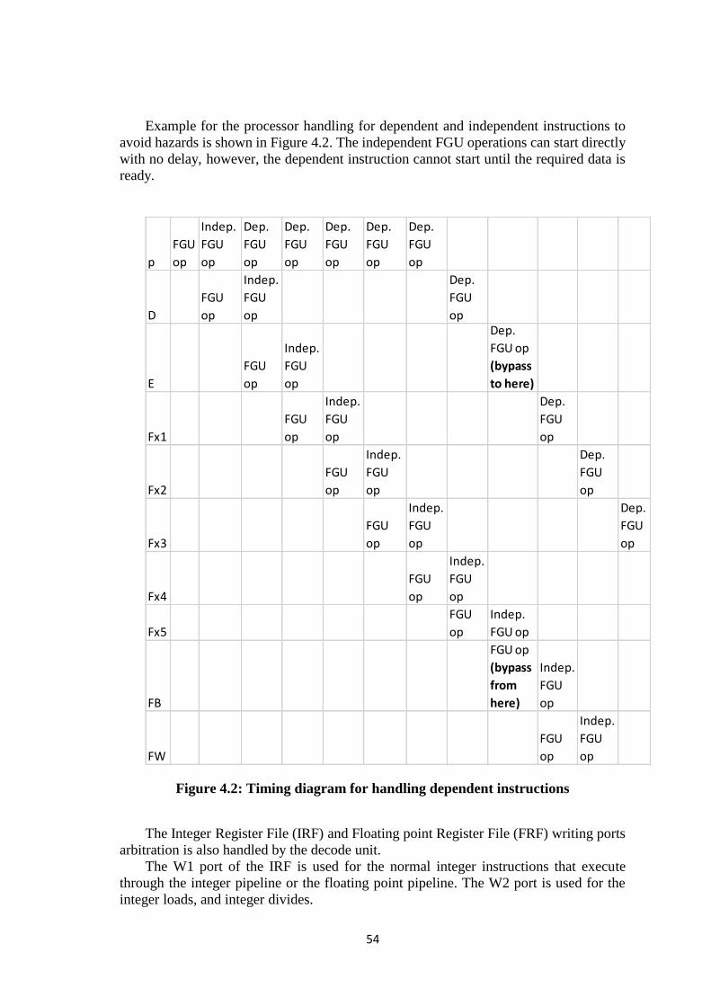
54
Example for the processor handling for dependent and independent instructions to
avoid hazards is shown in Figure 4.2. The independent FGU operations can start directly
with no delay, however, the dependent instruction cannot start until the required data is
ready.
Figure 4.2: Timing diagram for handling dependent instructions
The Integer Register File (IRF) and Floating point Register File (FRF) writing ports
arbitration is also handled by the decode unit.
The W1 port of the IRF is used for the normal integer instructions that execute
through the integer pipeline or the floating point pipeline. The W2 port is used for the
integer loads, and integer divides.
p
FGU
op
Indep.
FGU
op
Dep.
FGU
op
Dep.
FGU
op
Dep.
FGU
op
Dep.
FGU
op
Dep.
FGU
op
D
FGU
op
Indep.
FGU
op
Dep.
FGU
op
E
FGU
op
Indep.
FGU
op
Dep.
FGU op
(bypass
to here)
Fx1
FGU
op
Indep.
FGU
op
Dep.
FGU
op
Fx2
FGU
op
Indep.
FGU
op
Dep.
FGU
op
Fx3
FGU
op
Indep.
FGU
op
Dep.
FGU
op
Fx4
FGU
op
Indep.
FGU
op
Fx5
FGU
op
Indep.
FGU op
FB
FGU op
(bypass
from
here)
Indep.
FGU
op
FW
FGU
op
Indep.
FGU
op

55
The W1 port of the FRF is used for the normal floating point instructions that execute
through the floating point pipeline. The port W2 is used for floating-point loads and
floating-point divides.
4.3. Execution unit
Each thread group has a dedicated execution unit. The execution unit executes all
the integer and logical operations except for the integer multiplication and division
operations which are done in the FGU. The EXU also handles memory and branch
addresses as well as the integer source operand bypassing.
The EXU consists of the following subunits as shown in Figure 4.3:
Arithmetic Logic Unit (ALU)
Shifter (SHFT)
Operand Bypass (BYP)
Integer Register File (IRF)
Register Management Logic (RML)
Figure 4.3: EXU block diagram

56
4.4. Load Store Unit
The SPARC core has one LSU shared between the two thread groups. The LSU
handles all the memory reference between the core, the L1 cache and the L2 cache. All
the communication with the L2 cache is done through the cache crossbars (processor to
cache PCX and cache to processor CPX) through the gasket.
4.5. Cache Crossbar
The cache crossbar (CCX) unit connects the 8 SPARC cores to the 8 banks of the L2
cache. An additional port is used to connect the SPARC cores to the IO bridge. Maximum
number of simultaneous requests from the cores is 8, also the maximum number of data
return, acks, or invalidations coming from the L2 cache is 8.
The CCX is divided into two parts: processor to cache crossbar (PCX) and cache to
processor crossbar (CPX). The block diagram of the CCX unit is shown on Figure 4.4.
Figure 4.4: Communication between the SPARC core and the L2 cache through
the cache crossbar
4.6. Memory Management Unit
The Memory Management Unit (MMU) uses its hardware tablewalk state machine
to find valid Translation Table Entries (TTEs) for the requested access. The Translation
Lookaside Buffers (TLBs) use the TTEs to generate the Physical Addresses (PAs) from

57
Virtual Addresses (VAs) and Real Addresses (RAs). The TLBs use the TTEs to validate
that a request has the permission to access the requested address.
4.7. Trap Logic Unit
The Trap Logic Unit (TLU) manages exceptions, and traps for the SPARC core. The
thread may take a trap if some exceptions (conditions) occurred. The TLU keeps track of
the current processor state related to trap. The TLU maintains the trap table to be accessed
by the software to handle the trap correctly. The TLU prevents the update of architectural
state for the instructions after an exception, it relies on the IFU and execution units to
achieve this. The main blocks of the TLU are shown in Figure 4.5.
Figure 4.5: TLU basic blocks
The TLU consists of the following blocks:
The Flush logic: Responsible for generating flushes in response to exceptions
The Trap Stack Array (TSA) maintains the trap state for each of the eight
threads for up to six trap levels
The Trap State Machine prioritizes the trap requests for the eight threads

58
Examples for the different traps in the SPARC core are:
ECC errors on the source operands, this is detected in the execution unit,
LSU, or the FGU
Invalid or illegal instruction detected in the IFU
Exception reported on the floating point instruction, note that FGU sends the
trap prediction on the FX2 and the actual trap in FB stage of the pipeline. The
pipeline timing diagram for the case when the branch prediction is correct is
shown on Figure 4.6 and the case of the trap mis-predict is shown on Figure
4.7. In Figure 4.6, the trap is predicted in FX2 cycle, the FGUOp0 instruction
continues execution but the successive instructions are flushed. The actual
exception is calculated at FB cycle. In this case the prediction was correct so
the instruction was flushed. In Figure 4.7, where the predication was wrong
the instruction FGUOp0 completes successfully and the successive
instructions and restarted.

59
Figure 4.6: Correct trap prediction
p op2 op3 op4 op5
op6
flushed
by IFU
op7
flushed
by IFU
D op1 op2 op3 op4 op5
op6
flushed
by IFU
E/FRF FGUOp0 op1 op2 op3 op4
op5
flushed
by IFU
M/Fx1 FGUOp0 op1 op2 op3
op4
flushed
by IFU
B/Fx2
FGUOp0
(FGU
reports
exception
predition) op1 op2
op3
flushed
by IFU
W/Fx3
FGUOp0
(TLU
broadcasts
flush)
Op1
Flushed
by TLU
op2
flushed
by IFU
Fx4 FGUOp0
Fx5 FGUOp0
FB
FGUOp0
(FGU
reports
exception
to TLU)
FW
FGU
flushes
FGUOp0
(TLU
broadcasts
flush)
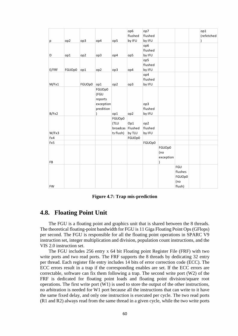
60
Figure 4.7: Trap mis-prediction
4.8. Floating Point Unit
The FGU is a floating point and graphics unit that is shared between the 8 threads.
The theoretical floating-point bandwidth for FGU is 11 Giga Floating Point Ops (GFlops)
per second. The FGU is responsible for all the floating point operations in SPARC V9
instruction set, integer multiplication and division, population count instructions, and the
VIS 2.0 instruction set.
The FGU includes 256 entry x 64 bit Floating point Register File (FRF) with two
write ports and two read ports. The FRF supports the 8 threads by dedicating 32 entry
per thread. Each register file entry includes 14 bits of error correction code (ECC). The
ECC errors result in a trap if the corresponding enables are set. If the ECC errors are
correctable, software can fix them following a trap. The second write port (W2) of the
FRF is dedicated for floating point loads and floating point division/square root
operations. The first write port (W1) is used to store the output of the other instructions,
no arbitration is needed for W1 port because all the instructions that can write to it have
the same fixed delay, and only one instruction is executed per cycle. The two read ports
(R1 and R2) always read from the same thread in a given cycle, while the two write ports
p op2 op3 op4 op5
op6
flushed
by IFU
op7
flushed
by IFU
op1
(refetched
)
D op1 op2 op3 op4 op5
op6
flushed
by IFU
E/FRF FGUOp0 op1 op2 op3 op4
op5
flushed
by IFU
M/Fx1 FGUOp0 op1 op2 op3
op4
flushed
by IFU
B/Fx2
FGUOp0
(FGU
reports
exception
predition
) op1 op2
op3
flushed
by IFU
W/Fx3
FGUOp0
(TLU
broadcas
ts flush)
Op1
Flushed
by TLU
op2
flushed
by IFU
Fx4 FGUOp0
Fx5 FGUOp0
FB
FGUOp0
(no
exception
)
FW
FGU
flushes
FGUOp0
(no
flush)

61
can write to the same or different threads. The FGU supports FRF bypassing for FGU
operations having FRF destination (excluding the division and square root operations).
The FGU is compliant with the IEEE 754 standard:
1. Single and double precision support, all quad precision instructions are not
supported
2. Support for all the data types (normal, subnormal, zero, NaN, and infinities) with
limitations in some instructions
3. Support for the IEEE required rounding modes
4. Support for the IEEE defined exceptions (invalid operation, inexact, division by
zero, overflow, and underflow)
The FGU block diagram is shown on Figure 4.8. The FGU consists of three
pipelines:
Floating point execution pipeline (FPX)
Graphics execution pipeline (FGX)
Floating point division and square root pipeline (FPD)
Figure 4.8: FGU block diagram
The FGX and FPX pipelines have throughput of one instruction per cycle and require
fixed number of cycles (6 cycles) regardless of the values of the operands to execute and
are fully pipelines except for the PDIST instruction, the FPD pipeline uses dedicated non-

62
pipelined unit but it is not blocking for the FPX and FGX pipelines. The floating point
division requires fixed number of cycles while integer division has variable delay
depending on the values of the operands. The PDIST instruction requires three sources
so it takes two cycles to fetch the sources for the FRF and no floating point operation can
start the cycle after the PDIST instruction.
The FGU design optimizes area and power by sharing the resources across different
paths, where the floating point add, multiply and division share the format and exponent
calculations. The FPX pipeline is shared with the graphics and integer data paths
whenever applicable (partitioned add/subtract reuse the floating point adder, the 8x16
multiply operations reuse the floating point multiplier, the integer multiplication and
division are also reusing the corresponding floating point units). The power is also
optimized by using clock gating mechanism to disable all the parts that are inactive. Four
clock domains are used in the FGU unit as shown in Table 4.2. The FGU pipelines details
are shown on Figure 4.9.
Figure 4.9: FGU pipelines
4.8.1. Interface with other units
The FGU interface with other units in the SPARC processor is explained in Figure
4.10. The IFU provides the instruction control information (part of the opcode) as well
as the sources and the destinations. Only one instruction can be issued to the FGU per

63
cycle. The IFU can flush the FGU in the FX2 or FX3 stages. The FGU provides the status
of the executed instruction to the IFU. The FGU sends the predicted trap and the actual
exception to the TLU. The TLU can send a flush at FX3 stage. The LSU shared the W2
port of the FRF with the FPD pipeline where FPD pipeline has higher priority since it
cannot stall. The FPD reserves the W2 port few cycles before the result is ready by
notifying the IFU and LSU about the expected completion of the instruction. The load
operation can update the FRF or the Floating-point State Register (FSR), the floating
point store instruction shared a read port of the FRF with the execution pipeline. The
FGU can execute integer instructions so it has interface with the two execution units as
shown in Figure 4.10. The EXU provides the integer sources as well as the Graphics State
Register (GSR) control signals to the FGU. The FGU writes the result back to the EXU
along with the destination address as provided by the IFU.
Figure 4.10: FGU interface with other units
Table 4.2: FGU clock domains
Clock Description
Main Any instruction requires FGU action enables this domain
Multiply Any floating point, integer, or VIS multiplication operations
Divide Any floating point or integer divide or square root
VIS Any VIS instruction executed in the FGX pipeline
4.8.2. Floating-Point State Register (FSR)
The FSR is maintained inside the FGU for each thread, the FSR is 64 bits which
includes different bits to control the FGU operation (round direction for example) as well
as bits to specify the status of the operation.

64
4.8.3. Conclusion
In this chapter we explained the overall OpenSparc T2 processor design. We have
also went through details for the main blocks in the SPARC core. In the next chapter we
will explain all the changes done in the processor to include the FMA unit.

65
Chapter 5 : Including the binary/decimal FMA in the
OpenSparc T2 processor
The FGU in the OpenSparc T2 has a good support for the binary floating point
arithmetic. However, the support for the binary floating point operations is missing the
FMA instructions. The FGU also has no support at all for the decimal floating point
arithmetic. Although all the unsupported operations can be handled at the software level,
but the cost in term of number of cycles to do the same function is huge compared to the
hardware support.
In our work we have integrated the binary/decimal FMA unit implemented in [7]
into the OpenSparc T2 processor thus improving the support of the processor’s floating
point unit by 11 more binary and decimal instructions.
The SPARC core units modified during our work are:
The gasket
Pick unit
Decode unit
FGU
TLU
In our work we have also added the newly supported instructions to the SPARC ISA
and updated the assembler software and recompiled it to work with the new instructions
correctly. All the changes have been verified on the OpenSparc T2 verification
environment which has been modified to test the newly added instructions.
5.1. Related work
In his master’s work M. Hosny [28] has integrated the decimal FMA unit developed
in [29] in the OpenSparc T2 processor. He has added the support for the new unit in the
processor architecture and updated the Instruction Set Architecture (ISA) for the new
decimal instructions supported on the hardware. The new instructions that he defined are:
Decimal Fused Multiply-Add double (DFMADDd)
Decimal Fused Multiply-Subtract double (DFSUBd)
Decimal Fused Negative Multiply-Add double (DFNMADDd)
Decimal Fused Negative Multiply-Subtract double (DFNMSUBd)
Decimal Floating point Add double (DFADDd)
Decimal Floating point Subtract double (DFSUBd)
Decimal Floating point Multiply double (DFMULd)
In his work he also updated the software tool chain to understand the new
instructions.
In our work we have integrated FMA unit that supports binary and decimal
operations into the OpenSparc T2 processor. The FMA unit that we added has less
delay (by ~ 12%) and additionally supports similar operations on the binary side.
Integrating of the new unit allows us to support the 4 new binary FMA operations
in addition to the 7 decimal operation that M. Hosny has supported in his work. In
addition because the FMA used supports binary multiplication and addition in

66
addition to the FMA operation, this allowed us to explore possible improvements
in the processor floating point unit to increase the throughput.
5.2. SPARC ISA update
The SPARC instruction set has been updated to include the newly supported
instructions. SPARC V9 provides two instructions that are entirely implementation
dependent: IMPDEP1 and IMPDEP2. The IMPDEP1 is used to implement many VIS
instructions in the UltraSparc architecture. In later releases of the SPARC architecture,
the IMPDEP2 was divided into two parts IMPDEP2A and IMPDEP2B where
IMPDEP2A remains implementation dependent while IMPDEP2B is used for the binary
FMA instructions.
We have used the IMPDEP1 instructions set to implement all the decimal operations
other than the FMA, and the IMPDEP2B to implement the binary and decimal FMA
operations. The Opcode for the implementation dependent instructions is shown in Table
5.1. The Op3 6 bits used to differentiate between the IMPDEP1 and IMPDEP2 are shown
in Table 5.2. The Op2 2 bits are used to differentiate between the IMPDEP2A and
IMPDEP2B as shown in Table 5.3.
Table 5.1: Opcode for the implementation dependent instructions
10 Impl-dep Op3 Impl-dep Op2 Impl-dep
31 30 29 25 24 19 18 7 6 5 4 0
Table 5.2: Op3 values for IMPDEP1 and IMPDEP2
Op3 Implementation dependent
110110 IMPDEP1
110111 IMPDEP2
Table 5.3: Op3 values for IMPDEP1 and IMPDEP2
Op2 Implementation dependent
00 IMPDEP2A
01,10,11 IMPDEP2B
The FMA operations have 4 operands which are: the destination register rd, first
source rs1, second source rs2 and third source rs3. The Opcode used for the FMA
operations is shown in Table 5.4.
Table 5.4: Opcode for the FMA instructions
10 rd 110111 rs1 rs3 Op5 rs2
31 30 29 25 24 19 18 14 13 9 8 5 4 0

67
The Op5 used for the FMA operations is shown in Table 5.5.
Table 5.5: Op5 values for FMA operations
Op5 Instruction Assembly
00 01 Multiply-Add single FMADDs
00 10 Multiply-Add double FMADDd
00 11 Decimal Multiply-Add DFMADDd
01 01 Multiply-Subtract single FMSUBs
01 10 Multiply-Subtract double FMSUBd
01 11 Decimal Multiply-Subtract DFMSUBd
10 01 Negative Multiply-Subtract single FNMSUBs
10 10 Negative Multiply-Subtract double FNMSUBd
10 11 Negative Decimal Multiply-Subtract DFNMSUBd
11 01 Negative Multiply-Add single FNMADDs
11 10 Negative Multiply-Add double FNMADDd
11 11 Negative Decimal Multiply-Add DFNMADDd
The decimal operations are implemented using the IMPDEP1 space, the opcode for
the IMPDEP1 is shown in Table 5.6 and the values of the Opf to differentiate between
the different instructions is shown in Table 5.7. Note that these operations have only 3
operands unlike the FMA instructions which are: the destination register rd, the first
source register rs1 and the second source register rs2.
Table 5.6: Opcode for IMPDEP1
10 rd 110110 rs1 Opf rs2
31 30 29 25 24 19 18 14 13 5 4 0
Table 5.7: Opf values for decimal operations
Opf Instruction Assembly
00000 0010 Decimal Addition DFADDd
00000 0110 Decimal Subtraction DFSUBd
01000 0010 Decimal multiplication DFMULd
Note that the above selection for the Opcode is done to match [28] so the user can
use the same compiler on both units.
In the next sections we will explain how the SPARC core was modified to support
the new unit and the new instructions. Our changes have affected multiple units in the
core and we will go through the changes in the next sections.

68
5.3. FGU changes
The new FMA unit integrated implements some of the functionalities of the original
FGU which are the binary addition and multiplication, and also supports some new
functionalities which are the binary and decimal FMA, decimal addition, multiplication
and subtraction. So we had different design decisions which are:
1. The new unit to replace the original unit functionality for the adder and multiplier
and we can remove their old implementation to decrease the core area. We
explored this possibility but we faced the following issues:
a. The new unit only supports binary 64 format, although in our future work
we plan to modify the unit to work also with binary 32 format but
currently the new unit cannot handle the 32 bits operations.
b. The multiplication unit in the FGU handles also integer multiplication
and SIMD operations, these cannot be handled with the new unit. The
same for addition.
c. As part of optimizing the core area, some parts like the exponent path is
shared between different instructions so cannot remove these shared units
even if the adder and multiplier are replaced with the new unit
2. The new unit can be integrated as a separate pipeline inside the FGU, this
approach can help in increasing the processor throughput since now we can have
two binary-binary or binary-decimal operations handled in parallel. However,
the support for extra pipeline in the FGU will increase the complexity and will
require a lot of modifications in the processor such as modifying the decode unit
to fetch two FGU instructions in the same cycle but the decode unit has to be
made smarter to differentiate between the types of the FGU instructions and
which of them can be handled in two units versus the ones that can be only
handled in one unit. The decode unit will also need to handle more types of
hazards that can occur because of the presence of the two units such as the
relations between the sources and the destinations of the two parallel instructions
may cause RAW or WAW. Also the current FRF used has to be changed or
enhanced since it only has two write ports and two read ports and all of them are
already reserved for current pipelines.
3. Use the new unit to support the new instructions, the old instructions will be
executed only through the original units. This is simpler approach that allow for
the addition of the new functionality without complicating things or breaking the
current support. In our future work we are studying the possibility to allow using
the new unit for multiplication operations that starts the cycle after a
multiplication operation is started. Currently the second instruction is blocked
and we can use the new unit to remove this limitation and improve the processor
throughput in this case. Another possible improvement is to overcome the
missing support for the subnormal numbers in the multiplication operation by
making use of the FMA unit in this case.
The new unit is integrated as a new block in the FGU, and the new instructions are
executed in the FPX pipeline. The new instructions read the data from the FRF and write
back the result to the FRF and the flags to the floating point state registers.
The FMA instructions require two cycles to read the data from the FRF before the
actual execution of the operation since the FMA instructions have three sources. This is
handled the same way the PDIST operation is handled since it also fetches the inputs
from the FRF in two cycles. This is handled in the decode unit where the three addresses
are sent to the FRF in two cycles.
69
The output of the FRF is used directly in the FMA unit without any formatting, this
is different from the other units where the data is formatted first before the operations.
The FMA unit does the full operation for both the exponent and the significand including
the final normalization and rounding. Also the sign is calculated inside the FMA unit so
the output of the FMA unit is connected directly to the FRF write port without any
modifications. The FMA flags are mapped to the corresponding bits of the state registers
and the state registers are updated with the result of the FMA unit. The state registers are
enabled per instruction since each instruction may have different set of corresponding
flags, state registers enabling conditions has been updated to understand the required
flags for the new instructions. Also the rounding mode supported by the processor is
mapped to the corresponding rounding directions of the FMA. The selop and bd inputs
of the FMA are set according to the instruction type. No special handling is needed to
support the decimal floating point numbers since they are encoded in 64 bits like the
binary double precision numbers and are saved in the same register file. Only the FMA
unit differentiates between the binary and decimal formats of the inputs.
The FGU sends a flag to the TLU when the PDIST operation is executed, this is
needed because the TLU needs to know the instructions that require two cycles to fetch
the operands from the FRF to be able to handle traps correctly. This flag has been updated
to consider the FMA operations as well since it also requires two cycles to fetch the
sources from the FRF.
New clock domain has been added to the FGU control unit to power on the FMA
unit using clock gating mechanism to save power, this is done similar to the
multiplication unit. Other changes has been done in the control paths to let the FMA
result go through the different multiplexers to reach the FRF.
5.4. Gasket changes
The cache crossbar (CCX) connects the 8 SPARC cores to the 8 banks of the L2
cache. All the processor to cache (PCX) and cache to processor (CPX) communication
is done via the gasket.
The gasket partially decodes the instructions read from the cache and invalidates the
incorrect instructions by replacing the first 5 bits of the opcode with zeros. The gasket
unit is updated to consider the newly added instructions as legal instructions.
5.5. Pick unit changes
The pick unit is modified to understand the new instructions and consider them as
floating point unit instructions. The pick unit also identifies what are the valid sources
and/or destination for each instruction, it is modified to be able to understand the FMA
instruction which is the only instruction that has 4 register file addresses in the opcode (3
for the sources and 1 for the destination).
Special handling is required for the FMA operations since the floating point register
file has only 2 read ports so 2 cycles are needed to get the input ready for the FMA
instruction, the pick unit detects the instructions that need two cycles to fetch input and
sends flag to the decode unit. The pick unit also has dependency check for Write After
Write (WAW) and Read After Write (RAW) hazards; this is done by comparing the
source and destinations of the new instructions with the ones already executing in the

70
pipeline, the check has been updated to consider the hazards that can occur from the FMA
third operand.
5.6. Decode unit changes
The decode unit is changed to prevent any floating point instructions from being
executed the cycle after FMA instructions to avoid hazard at the floating point register
file read ports.
The decode unit extracts the sources and the destination from the new instructions
and send them to the floating point unit, the decode unit save the third source of the FMA
instruction in a register to be sent in the next cycle to the floating point unit.
5.7. TLU unit changes
The TLU needs to know about the instructions that take two cycles to fetch inputs
from the FRF to handle the trap correctly. New flag is sent to the TLU to indicate that
FMA instruction is being executed.
5.8. Software changes
The verification environment that is coming with the OpenSparc T2 has different
diags that are used to test the functionality of the processors. These diags are written in
assembly language and are compiled using the assembler to generate the executable file.
The executable file is then dumped in opcode format to be loaded to the processor
memory during simulation.
Since the new instructions that we added are not understood by the assembler we
were not able to test our changes using the assembly tests and instead we used to modify
the memory image files manually to test the changes. As a fix for this limitation we have
updated the assembler code to understand the new instructions and generate the
corresponding opcode correctly. The GNU Binutils version 2.21.1 has been downloaded,
modified and recompiled. The modified assembler is then added to the processor
verification tools to be used in the regression tests.
As an example for the software changes we will show the changes done to enable
the FMADDd instruction. The other instructions are similar to this.
The changes are done in three BinUtils sources files:
include/opcode/sparc.h: This is the header file for the sparc opcode data
structure definitions as well as the mapping functions for the opcode. This
file was modified to support new instruction type with 4 operands.
gas/config/tc-sparc.c: This file is the source code for the GNU assembler.
This file is modified to be able to understand the fourth operand passed to the
instruction.
opcodes/sparc-opc.c: This file includes all the assembly instructions
supported in the SPARC architecture and the function used to decode them
into their opcode. This file is modified to define the new instructions.

71
5.8.1. include/opcode/sparc.h changes
This file was modified as shown in Figure 5.1. Three modifications have been
applied to the file which are:
The op5 part of the opcode that we used in IMPDEP2A instructions set is
defined. Note that in the definition of this field we specify both the location
and the size. The location is defined by the shift amount done so in this case
the field position is 5. The size of the field is defined by the number of ones
in the “&” operation with x, in this case the size is 4 since 0xf is the
hexadecimal representation of 1111.
The rs3 operand in the opcode is also defined as a new operand in this file,
similar to the explanation for op5, rs3 is in the 9th bit with size of 5 bits.
The last modification in the file to support the FMA instruction is the
definition of the new format F4F that includes the part of the opcode that is
used to decode the instructions. For the FMA operation the op, op3 and op5
fields are used together to decode the instruction.
***************
*** 193,202 ****
--- 193,204 ----
#define OP2(x) (((x) & 0x7) << 22) /* Op2 field of format2 insns. */
#define OP3(x) (((x) & 0x3f) << 19) /* Op3 field of format3 insns. */
+ #define OP5(x) (((x) & 0xf) << 5) /* Op5 field of format5 insns. */
#define OP(x) ((unsigned) ((x) & 0x3) << 30) /* Op field of all insns. */
#define OPF(x) (((x) & 0x1ff) << 5) /* Opf field of float insns. */
#define OPF_LOW5(x) OPF ((x) & 0x1f) /* V9. */
#define F3F(x, y, z) (OP (x) | OP3 (y) | OPF (z)) /* Format3 float insns. */
+ #define F4F(x, y, z) (OP (x) | OP3 (y) | OP5 (z)) /* Format4 float insns. */
#define F3I(x) (((x) & 0x1) << 13) /* Immediate field of format 3 insns.
*/
#define F2(x, y) (OP (x) | OP2(y)) /* Format 2 insns. */
#define F3(x, y, z) (OP (x) | OP3(y) | F3I(z)) /* Format3 insns. */
***************
*** 204,209 ****
--- 206,212 ----
#define DISP30(x) ((x) & 0x3fffffff)
#define ASI(x) (((x) & 0xff) << 5) /* Asi field of format3 insns. */

72
#define RS2(x) ((x) & 0x1f) /* Rs2 field. */
+ #define RS3(x) (((x) & 0x1f) << 9) /* Rs3 field. */
#define SIMM13(x) ((x) & 0x1fff) /* Simm13 field. */
#define RD(x) (((x) & 0x1f) << 25) /* Destination register field. */
#define RS1(x) (((x) & 0x1f) << 14) /* Rs1 field. */
Figure 5.1: include/opcode/sparc.h changes
5.8.2. opcodes/sparc-opc.c changes
The modifications in this file are shown in Figure 5.2. The new instruction fmaddd
is added which uses the new format type F4F that we defined in sparc.h. Note that the
values passed to the F4F corresponds to the values of op, op3, and op5 for the fmaddd
operation (op=10, op3=0110111,op5=10). The four values “v,B,4,H” used are flags
corresponding to the types of the operands. The definition for these flags is in
gas/config/tc-sparc.c. The “v” means that the first operand is 64 bits floating point
register corresponding to RS1 position in the opcode, the “B” means that the second
operand is 64 bits floating point register corresponding to the RS2 position in the opcode,
the “4” means that the third operand is 64 bits floating point register corresponding to the
RS3 position in the opcode, finally the “H” means that the destination is a 64 bits floating
point register corresponding to the RD field position in the opcode.
***************
*** 1809,1814 ****
--- 1809,1817 ----
{ "siam", F3F(2, 0x36, 0x081), F3F(~2, ~0x36, ~0x081)|RD_G0|RS1_G0|RS2(~7),
"3", 0, v9b },
+ /* FMA unit instructions */
+ { "fmaddd", F4F(2, 0x37, 0x02), F4F(~2, ~0x37, ~0x02), "v,B,4,H",
F_FLOAT, v9 },
+
/* More v9 specific insns, these need to come last so they do not clash
with v9a instructions such as "edge8" which looks like impdep1. */
Figure 5.2: opcodes/sparc-opc.c changes

73
5.8.3. gas/config/tc-sparc.c changes
The modifications done in this file are shown in Figure 5.3. The modifications done
are mainly to define the new operand type ‘4’ that we used in sparc-opc.c file. The new
value RS3 was defined in sparc.h as explained previously.
***************
*** 2131,2136 ****
--- 2131,2137 ----
case 'e': /* next operand is a floating point register */
case 'v':
case 'V':
+ case '4':
case 'f':
case 'B':
***************
*** 2153,2158 ****
--- 2154,2160 ----
if ((*args == 'v'
|| *args == 'B'
+ || *args == '4'
|| *args == 'H')
&& (mask & 1))
{
***************
*** 2213,2218 ****
--- 2215,2223 ----
case 'R':
opcode |= RS2 (mask);
continue;
+ case '4':
+ opcode |= RS3 (mask);
+ continue;
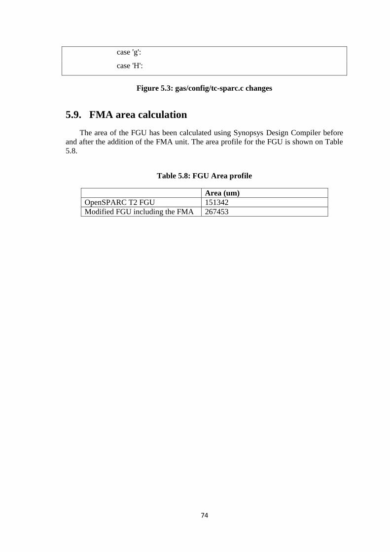
74
case 'g':
case 'H':
Figure 5.3: gas/config/tc-sparc.c changes
5.9. FMA area calculation
The area of the FGU has been calculated using Synopsys Design Compiler before
and after the addition of the FMA unit. The area profile for the FGU is shown on Table
5.8.
Table 5.8: FGU Area profile
Area (um)
OpenSPARC T2 FGU 151342
Modified FGU including the FMA 267453

75
Chapter 6 : Conclusion and future work
In this research, we have integrated the binary/decimal FMA unit developed in [7]
in the open-source processor OpenSparc T2. This allowed us to support 11 new floating
point instructions in the processor ISA. The support of the new instructions in the
processor helps in improving the overall processing time as well as the power
consumption.
The modifications in the OpenSparc T2 processor are scattered across different units,
the results have been verified using the simulation verification environment that came
with the processor. New assembly tests have been created to verify the new instructions.
The SPARC ISA in the GNU assembler has been updated and rebuilt to support the
new set of added instructions.
We have worked on verifying the FMA unit as a standalone unit as well as after
integration in the processor. We proposed a new verification checker for binary floating
point multiplication that is applicable to any floating point unit; the checker can be used
in formal or simulation runs and has uncovered many bugs in the unit. We have fixed
some of found bugs and the others are still under investigation. The checker has been
applied on other open source designs and proved its capability of detecting corner cases
bugs.
As for the future work, the FMA unit can be modified to support the binary single
precision format, this allows for the support of the three remaining FMA instructions in
the processor. The verification flow proposed can also be extended to support other
binary and decimal floating point operations. The developed checker can be applied other
designs to help in verifying their functionality.
The OpenSparc T2 FGU unit has some limitation in the multiplication operation that
can be addressed with the usage of the new integrated unit. Examples for the current
limitations:
1. Two successive multiplication instructions is not supported
2. Subnormal support in the multiplication is incomplete
76
References
[1] P. E. Ceruzzi, “A History of Modern Computing,” in the MIT Press, 2003.
[2] L. K. Wang, C. Tsen, M. J. Schulte, and D. Jhalani, “Benchmarks and performance
analysis of decimal floating-point applications,” in the
25th IEEE International Conference on Computer Design (ICCD-25), pp.
164 –170, Oct. 2007.
[3] H. A. H. Fahmy, R. Raafat, A. M. Abdel-Majeed, R. Samy, T.
ElDeeb, and Y. Farouk, “Energy and delay improvement via decimal floating point
units,” in the 19th IEEE Symposium on Computer Arithmetic
(ARITH-19), pp. 221 –224, June 2009.
[4] IBM, “704 Data Processing System”, available at http://www-
03.ibm.com/ibm/history/exhibits/mainframe/mainframe_PP704.html.
[5] P. K. Monsson, “Combined binary and decimal floating-point unit,” MSc. thesis,
Technical University of Denmark, 2008.
[6] “IEEE Standard for Floating-Point Arithmetic,” IEEE Std 754-2008, pp. 1–58, Aug
2008.
[7] A. Adel, “IEEE-Compliant Binary/Decimal unit based on a binary/Decimal FMA,”
MSc. Thesis, Cairo University, 2014.
[8] L. Dadda, "Multioperand Parallel Decimal Adder: A Mixed Binary and BCD
Approach," in Computers, IEEE Transactions on , vol.56, no.10, pp.1320-1328, Oct.
2007.
[9] K. Yehia, “A Mixed Decimal/Binary Redundant Floating-Point Adder,” MSc.
Thesis, Cairo University, 2011.
[10] A. Verma, P. Brisk, and P. Ienne, “Hybrid LZA: A near optimal implementation of
the leading zero anticipator,” in Design Automation Conference, 2009. ASP-DAC
2009. Asia and South Pacific, pp. 203–209, Jan 2009.
[11] A. Sayed-Ahmed, H. Fahmy, and M. Hassan, “Three engines to solve verification
constraints of decimal floating-point operation,” in Signals, Systems and Computers
(ASILOMAR), 2010 Conference Record of the Forty Fourth Asilomar Conference on,
pp. 1153–1157, 2010.
[12] K. Nouh, H. Fahmy, “Binary Floating Point Verification Using Random Test
Vector Generation Based on SV Constraints”, in IEEE International Conference on
Electronics, Circuits, and Systems, December 2015.

77
[13] Y-A. Chen, R.E. Bryant, "*PHDD: an efficient graph representation for floating
point circuit verification," in Computer-Aided Design, IEEE/ACM International
Conference, pp.2-7, November 1997.
[14] M.D. Aagaard, C.-J.H. Seger, "The formal verification of a pipelined double-
precision IEEE floating-point multiplier," in Computer-Aided Design, IEEE/ACM
International Conference, pp.7-10, November 1995.
[15] R. Kaivola, N. Narasimhan, "Formal verification of the Pentium(R) 4 multiplier,"
High-Level Design Validation and Test Workshop, Sixth IEEE International, pp.115-
120, 2001.
[16] D. M. Russinoff, “A mechanically checked proof of IEEE compliance of the
floating point multiplication, division and square root algorithms of the AMD-K7
processor,” London Mathematical Society Journal of Computational Mathematics,
pp.148–200, 1998.
[17] N. Kikkeri, P.-M. Seidel, "Optimized Arithmetic Hardware Design based on
Hierarchical Formal Verification," in Electronics, Circuits and Systems, ICECS '06
13th IEEE International Conference, pp.541-544, December 2006.
[18] Q. Wang, X. Song, W.N. Hung, M. Gu, J. Sun, "Scalable Verification of a Generic
End-Around-Carry Adder for Floating-Point Units by Coq," in Computer-Aided Design
of Integrated Circuits and Systems, IEEE Transactions, vol.34, no.1, pp.150-154,
January 2015.
[19] J. Pan, K.N. Levitt, "A Formal Specification of the IEEE Floating-Point Standard
with Application to the Verification of Floating-Point Coprocessors," Signals, Systems
and Computers, Conference Record Twenty-Fourth Asilomar Conference, vol.1,
pp.505, November 1990.
[20] C. Berg and C. Jacobi, “Formal verification of the VAMP floating point unit,” in
CHARME, 2001.
[21] E.M. Clarke, M. Khaira, X. Zhao, "Word level model checking-avoiding the
Pentium FDIV error," Design Automation Conference Proceedings 1996, 33rd ,
pp.645-648, 3-7 Jun, 1996.
[22] Y.-A. Chen, R. Bryant, “Verification of floating-point adders,” in A. J. Hu and
M. Y. Vardi, editors, Workshop on Computer-Aided Verification, pages 488–499, July
1998.
[23] C. Jacobi, K. Weber, V. Paruthi, and J. Baumgartner, "Automatic Formal
Verification of Fused-Multiply-Add FPUs", Design Automation and Test in Europe
proceedings, pp.1298-1303, 2005.

78
[24] U. Krautz, V. Paruthi, A. Arunagiri, S. Kumar, S. Pujar, T. Babinsky, "Automatic
verification of Floating Point Units," in Design Automation Conference (DAC), 51st
ACM/EDAC/IEEE, pp.1-6, June 2014.
[25] “IEEE Standard for SystemVerilog--Unified Hardware Design, Specification, and
Verification Language”, IEEE Std 1800-2009, pp. 1-1285, 2009.
[26] Mentor Graphics, “Questa Autocheck”, available at
https://www.mentor.com/products/fv/questa-autocheck.
[27] Mentor Graphics, “Questa Formal”, available at
https://www.mentor.com/products/fv/questa-formal.
[28] M. Hosny, “Including a decimal floating point unit in an open-source processor
and patching its compiler”. MSc. Thesis, Cairo University, 2012.
[29] A. EL-Tantawy, “Decimal floating point arithmetic unit based on a fused multiply
add module”. MSc. Thesis, Cairo University, 2011.
[30] Oracle, “OpenSPARC T1 Micro Architecture Specification,” available at
http://www.oracle.com.
[31] Oracle, “OpenSPARC T2 Micro Architecture Specification,” available at
http://www.oracle.com.
[32] Oracle, “SPARC Assembly Language Reference Manual”, available at
http://www.oracle.com.
[33] Sun Microsystems, “The VIS Instruction Set”, white paper, 2002.
[34] Oracle, “UltraSPARC Architecture 2007”, available at http://www.oracle.com.
[35] Oracle, “Oracle SPARC Architecture 2011”, available at http://www.oracle.com.

أ
ملخصال
مفتوح معالج في مدمجة وجمع ضرب ةوحدأضافة لىع الرسالة هذه في العمل يتركز مما والعشرية الثنائية لالعداد العائمة النقطة ذات العمليات الجديدة الوحدة تدعم حيثر المصد
المدمجة الجمعو الضرب للعمليات يفتقر كان حيث للمعالج الحسابية الخصائص إستكمال لنا يتيحة. سابية ذات النقطة العائمة لألرقام العشريللدعم األولى للعمليات الح الضافةاب الثنائية لالرقام
لألرقام وحدات الحساباتالوحدة المدمجة تحسن من أستخدام المساحة و الطاقة عن طريق دمج العشرية و الثنائية.
معالج يساعد في تحسين وقت المعالجة الكلي، مقارنة معال دعم المزيد من الوظائف فى ريق إعادة طالمساحة المطلوبة عن تقليل يمكن .الوظائف نفسألداء تطبيقات البرمجيات أستخدام
أيضا باستخدام أحدث التكنولوجيا مع حجم أصغر يمكن . وحدات في عمليات مختلفةالاستخدام .أن تقلل من المساحة الكلية المطلوبة
ل اخدة الجديدة وحدالجديدة، ودمج العمليات المعالج لدعم التعديل تعليمات ويشمل العمل ليفهم التعليمات الجديدة و يتواصل بشكل المعالج عديلالمعالج، وت فىوحدة الفاصلة العائمة
.جديدةالت تعليماالفهم يلالمترجم تعديلتم يتضمن أيضا لعمل الذي ا .جديدةالحدة صحيح مع الو من حقق تم التو اختبارات جديدة، أضافةلمعالج عن طريق ل الجديدةوظائف التم التحقق من
.األختبارات القديمة بأستخداممعالج ال بعد تعديل وظائف القديمةالصالحية
ى المبنى عل الرسمى باستخدام تقنية التحقق مدمجة وجمع ضرب ةوحدتم التحقق من خالل عملنا اقترحنا أيضا منهجية للتحقق من .العديد من األخطاء في التنفيذ أساس رياضى حيث تم أكتشاف
.المبنى على أساس رياضى الرسمى التحققالعائمة باستخدام وحدة الفاصلة

محمد على اسماعيل على أحمد :دسـمهن 1987\2\4 تاريخ الميالد:
مصرى الجنسية: 2010\10\01 تاريخ التسجيل:
2016 تاريخ المنح: الكهربية واالتصاالت اإللكترونيات هندسة القسم: العلوم ماجستير الدرجة: ن:المشرفو
فهمى حسن على حساما.د.
الممتحنون:
)المشرف الرئيسي( فهمى حسن على حسام أ.د ابراهيم محمد قمر )الممتحن الداخلي( أ.د الهندسة، كلية )الممتحن الخارجي( سالم الفرغلى محمد محمد أشرف أ.د
شمس عين جامعة
عنوان الرسالة: المصدر مفتوح معالج فى العائمة طةالنق ذات مدمجة جمع و ضرب وحدة دعم
الكلمات الدالة:
تعليمات ، معالج، العائمة النقطة ذات مدمجة جمع و ضرب وحدة، العائمة النقطة ذات وحدة التحقق، المعالج
:رسالةملخـص ال
يثحر المصد مفتوح معالج في مدمجة وجمع ضرب ةوحد أضافة لىع الرسالة هذه في العمل يتركزويشمل العمل تعديل .والعشرية الثنائية لالعداد العائمة النقطة ذات العمليات الجديدة الوحدة تدعم
تعليمات المعالج لدعم العمليات الجديدة، ودمج الوحدة الجديدة داخل وحدة الفاصلة العائمة فى المعالج، لذي تم دة الجديدة. العمل اوتعديل المعالج ليفهم التعليمات الجديدة و يتواصل بشكل صحيح مع الوح
جمعالو ضربال ةوحدخالل عملنا تم التحقق من .يتضمن أيضا تعديل المترجم ليفهم التعليمات الجديدةباستخدام تقنية التحقق الرسمى المبنى على أساس رياضى حيث تم أكتشاف العديد من مدمجةال
الفاصلة العائمة باستخدام التحقق الرسمى اقترحنا أيضا منهجية للتحقق من وحدة .األخطاء في التنفيذ .المبنى على أساس رياضى

المصدر مفتوح معالج فى العائمة النقطة ذات مدمجة جمع و ضرب وحدة دعم
اعداد
محمد على اسماعيل على أحمد
القاهرة جامعة - الهندسة كلية إلى مقدمة رسالة
علومالماجستير درجة على الحصول متطلبات من كجزء
في
الكهربية واالتصاالت اإللكترونيات هندسة
:يعتمد من لجنة الممتحنين
لمشرف الرئيسىا فهمي حسن علي حساماالستاذ الدكتور:
الداخلي الممتحن قمر محمد إبراهيماالستاذ الدكتور:
كلية ،الخارجيالممتحن سالم ىالفرغل محمد محمد أشرفاالستاذ الدكتور:
شمس عين جامعة الهندسة،
القاهــرة جامعــة - الهندســة كليــة
العربيــة مصـر جمهوريـة - الجيـزة
2016

المصدر مفتوح معالج فى العائمة النقطة ذات مدمجة جمع و ضرب وحدة دعم
اعداد
محمد على اسماعيل على أحمد
القاهرة جامعة - الهندسة كلية إلى مقدمة رسالة
العلومماجستير درجة على الحصول متطلبات من كجزء
في
الكهربية واالتصاالت اإللكترونيات هندسة
تحت اشراف
فهمى حسن علي حسام .د .ا
واالتصاالت اإللكترونيات هندسة
الكهربية
القاهرة جامعة - الهندسة كلية
القاهــرة جامعــة - الهندســة كليــة
العربيــة مصـر جمهوريـة - الجيـزة
2016

المصدر مفتوح معالج فى العائمة النقطة ذات مدمجة جمع و ضرب وحدة دعم
اعداد
محمد على اسماعيل على أحمد
القاهرة جامعة - الهندسة كلية إلى مقدمة رسالة
العلومتيرماجس درجة على الحصول متطلبات من كجزء
في
الكهربية واالتصاالت اإللكترونيات هندسة
القاهــرة جامعــة - الهندســة كليــة
العربيــة مصـر جمهوريـة - الجيـزة
2016
Related Documents