MnO 2 ultrathin films deposited by means of magnetron sputtering: Relationships between process conditions, structural properties and performance in transparent supercapacitors Michal A. Borysiewicz * , Marek Wzorek, Marcin My sliwiec, Jakub Kaczmarski, Marek Ekielski Instytut Technologii Elektronowej, Al. Lotnik ow 32/46, 02-668 Warszawa, Poland article info Article history: Received 1 November 2016 Accepted 2 November 2016 Available online 4 November 2016 Keywords: MnO 2 Magnetron sputtering Transparent electronics Supercapacitor Ultracapacitor Sputtering ZnO Wearable electronics abstract This study focuses on the relationships between the process parameters during magnetron sputter deposition of MnO 2 and the resulting film properties. Three MnO 2 phases were identified - g, b and l and the dependence of MnO 2 phase presence on the oxygen content in the sputtering atmosphere was found. Selected MnO 2 phases were subsequently applied as ultrathin coatings on top of nanostructured ZnO electrodes for transparent super- capacitors with LiCl-based gel electrolyte. The films containing l-MnO 2 exhibited both the highest optical transparency of 62% at 550 nm as well as the highest specific capacitance in the supercapacitor structure, equal to 73.1 mF/cm 2 . Initially lower, the capacitance was elevated by charge-discharge conditioning. © 2016 The Authors. Published by Elsevier Ltd. This is an open access article under the CC BY license (http://creativecommons.org/licenses/by/4.0/). 1. Introduction Manganese dioxide is one of the most relevant compounds for modern energy storage devices, applied as electrodes both in the widespread Li-ion batteries [1,2] as well as in supercapacitor structures [3], due to its significant charge storage ca- pabilities combined with chemical stability, abundance and low cost. The material crystallizes in many polymorphic forms, among which a, b, g, d and l are the most known. The forms differ by the crystalline structure, in particular possess different types of angstrom-size tunnels, beneficial for ion intercalation in electrochemical energy storage devices [4]. Most MnO 2 materials are synthesized using the wet-chemical route and the current focus of study lies in MnO 2 nanostructures fabricated by a wide array of methods. At the same time, there is growing interest in micro power sources, fabricated using conventional microelectronic pro- cessing techniques for wearable devices [5]. One of such techniques is magnetron sputtering, compatible with conventional lithography and microprocessing requirements. * Corresponding author. E-mail address: [email protected] (M.A. Borysiewicz). Contents lists available at ScienceDirect Superlattices and Microstructures journal homepage: www.elsevier.com/locate/superlattices http://dx.doi.org/10.1016/j.spmi.2016.11.002 0749-6036/© 2016 The Authors. Published by Elsevier Ltd. This is an open access article under the CC BY license (http://creativecommons.org/licenses/by/4. 0/). Superlattices and Microstructures 100 (2016) 1213e1220

Welcome message from author
This document is posted to help you gain knowledge. Please leave a comment to let me know what you think about it! Share it to your friends and learn new things together.
Transcript
Superlattices and Microstructures 100 (2016) 1213e1220
Contents lists available at ScienceDirect
Superlattices and Microstructures
journal homepage: www.elsevier .com/locate/superlat t ices
MnO2 ultrathin films deposited by means of magnetronsputtering: Relationships between process conditions,structural properties and performance in transparentsupercapacitors
Michał A. Borysiewicz*, Marek Wzorek, Marcin My�sliwiec, Jakub Kaczmarski,Marek EkielskiInstytut Technologii Elektronowej, Al. Lotnik�ow 32/46, 02-668 Warszawa, Poland
a r t i c l e i n f o
Article history:Received 1 November 2016Accepted 2 November 2016Available online 4 November 2016
Keywords:MnO2
Magnetron sputteringTransparent electronicsSupercapacitorUltracapacitorSputteringZnOWearable electronics
* Corresponding author.E-mail address: [email protected] (M.A. Borysie
http://dx.doi.org/10.1016/j.spmi.2016.11.0020749-6036/© 2016 The Authors. Published by Elsevie0/).
a b s t r a c t
This study focuses on the relationships between the process parameters during magnetronsputter deposition of MnO2 and the resulting film properties. Three MnO2 phases wereidentified - g, b and l and the dependence of MnO2 phase presence on the oxygen contentin the sputtering atmosphere was found. Selected MnO2 phases were subsequently appliedas ultrathin coatings on top of nanostructured ZnO electrodes for transparent super-capacitors with LiCl-based gel electrolyte. The films containing l-MnO2 exhibited both thehighest optical transparency of 62% at 550 nm as well as the highest specific capacitance inthe supercapacitor structure, equal to 73.1 mF/cm2. Initially lower, the capacitance waselevated by charge-discharge conditioning.© 2016 The Authors. Published by Elsevier Ltd. This is an open access article under the CC
BY license (http://creativecommons.org/licenses/by/4.0/).
1. Introduction
Manganese dioxide is one of the most relevant compounds for modern energy storage devices, applied as electrodes bothin the widespread Li-ion batteries [1,2] as well as in supercapacitor structures [3], due to its significant charge storage ca-pabilities combined with chemical stability, abundance and low cost. The material crystallizes in many polymorphic forms,among which a, b, g, d and l are the most known. The forms differ by the crystalline structure, in particular possess differenttypes of angstrom-size tunnels, beneficial for ion intercalation in electrochemical energy storage devices [4]. Most MnO2materials are synthesized using the wet-chemical route and the current focus of study lies in MnO2 nanostructures fabricatedby a wide array of methods.
At the same time, there is growing interest in micro power sources, fabricated using conventional microelectronic pro-cessing techniques for wearable devices [5]. One of such techniques is magnetron sputtering, compatible with conventionallithography and microprocessing requirements.
wicz).
r Ltd. This is an open access article under the CC BY license (http://creativecommons.org/licenses/by/4.
M.A. Borysiewicz et al. / Superlattices and Microstructures 100 (2016) 1213e12201214
There are not much literature information on magnetron sputtering of MnO2. In 1972 Landorf et al. used an 800 diameterMn cathode for deposition of MnO2 on glass slides in an oxygen atmosphere at 2.7 Pa, using RF voltages of 1.5e3 kV andcurrents 0e45 mA for application in thin film capacitors [6]. The substrates were kept at temperatures between 140 and230 �C. X-ray diffraction patterns of the films contained lines that could be ascribed to either b-MnO2 or g-MnO2. The filmshad densities of around 3.0 g/cm3, significantly lower than the theoretical 5.0 g/cm3. Subsequently, in 1994 Fau et al. [7]deposited the material at 200 W RF power using a 80 mm diameter MnO2 target under 2 Pa total pressure and 13:2 Arto O2 flow ratio obtaining, as the previous authors, either b-MnO2 or g-MnO2 phase. In newer reports, Zhang et al. studiedMnO2 on Al2O3 for gas sensing purposes [8]. They deposited the material using a 35 mm MnO2 target under 200 W RFpower, 5 Pa total pressure and 9:1 Ar to O2 flow ratios. Yielding a ‘coarse’ microstructure on top of the Al2O3 substratesused. XRD patterns yielded MnO2 identified only as ‘tetragonal’, which most probably is b-MnO2. Finally, Li et al. studiedMnO2 deposition on copper using a Mn target with reactive deposition in an argon-oxygen mixture (7:3 Ar to O2 flow ratioand a pressure of 0.8 Pa) and found X-ray amorphous material with small grains of 10 nm diameter, however they did notstudy the grain structure [9].
These reports focused on single, arbitrary chosen process conditions to deposit the MnO2 films, and then put more weighton other behavior of the material, e.g. in devices. Therefore, we decided to provide in this communication a systematic studyof the process conditions influencing the properties of the MnO2 films deposited by reactive RF magnetron sputtering, withemphasis on structural properties and phase identification. We decided to combine the properties of the deposited materialwith the performance of transparent supercapacitors based on nanoporous ZnO electrodes coated with the MnO2 to meet thecommon applications of the material.
Transparent power sources are an interesting concept, deriving directly from the rapid development of transparentelectronics, in particular transparent displays. In transparent wearable devices (e.g. enhanced contact lenses or glasses)not only the display should be transparent, but also the whole device including the power source. The works concerningtransparent supercapacitors focus mostly on very thin carbon film electrodes due to the high capacitance ofconventional carbon electrodes. The usual reports see specific capacitances of around 1 mF/cm2 with transparencyaround 50% [10,11].
In our investigation, we decided to form the porous electrode using the intrinsically transparent ZnO semiconductor [12]in order to achieve high capacitance through an increased surface area and then to coat it with MnO2 for capacitanceenhancement by ion intercalation. We wanted to see which process parameters would lead to the formation of MnO2 phasesyielding the highest capacitance in such a system. The high transparency of the device is maintained by a low MnO2 filmthickness set at 10 nm.
2. Experimental
The experiment was divided into two parts. First, MnO2 thin films were deposited by magnetron sputtering and theirstructural properties were studied. Secondly, a part of the MnO2 films was selected to be deposited on top of transparentporous ZnO films to be used as transparent electrodes of a supercapacitor.
The MnO2 sputter deposition was carried out in a Surrey NanoSystems g-1000C reactor using a 75 mm diameter MnO2target under 125 W RF power. The target to substrate distance was 15 cm. In the experiment, the total gas pressure was 0.2,0.4, 0.8 or 1.6 Pa and the atmosphere was composed of 10 sccm Ar and 0, 1 or 5 sccm of O2. The total pressure and gas flowswere controlled independently by the application of a throttle valve. During sputtering, a Hiden ESPion Langmuir probe wasused to monitor the plasma parameters. Film thicknesses and densities were determined using X-ray reflectometry (XRR) ona PANalytical Empyrean 2 equipped with Cu Ka radiation, a 2-Ge monochromator with a mirror and a Pixcel detector.Structural information was derived from transmission electron microscopy (TEM) on a JEOL JEM-2100 using imaging andselected area electron diffraction (SEAD) of the material deposited directly on TEM carbon grids. Since the deposition rateswere very low, conventional X-ray diffraction was not feasible with the ultrathin films achieved.
Based on the structural analysis, a set of parameters was chosen to deposit 10 nm - thick MnO2 films on porous ZnO/FTO-glass electrodes and supercapacitors were fabricated. The porous ZnO films of 450 nm thickness were fabricated usingmagnetron reactive sputtering of a Zn target in an Ar:O2 atmosphere in the same reactor with postdeposition oxidation in anoxygen flow at 400 �C for 5min - a process we described earlier [13]. Since the ZnO formed in this manner is highly resistive, asecond annealing in an argon-hydrogenmixturewas applied to dope the ZnO, as hydrogen forms a shallow donor in ZnO [12].An optimized temperature of 350 �C and time of 30 s was chosen. The supercapacitors were assembled of two symmetricalelectrodes, in-between which a frame of a double-sided 100 mm thick adhesive tape was applied serving both as the electricseparator and sealant. A poly(vinyl alcohol) (PVA) and LiCl gel electrolyte was used in the supercapacitors. To prepare theelectrolyte, 20 ml of H2O were heated to 95 �C. Next, 2 g of PVA were added with mechanical mixing. After the mixturebecame homogeneous, 4.25 g of LiCl were added followed by vigorous mixing. Cyclic voltammetry tests were performed toassess supercapacitor performance using a Gamry Reference 3000 potentiostat. The optical transmission was determinedusing a Sentech SE 800E spectral ellipsometer. Stability tests were performed for 5000 charge/discharge cycles.
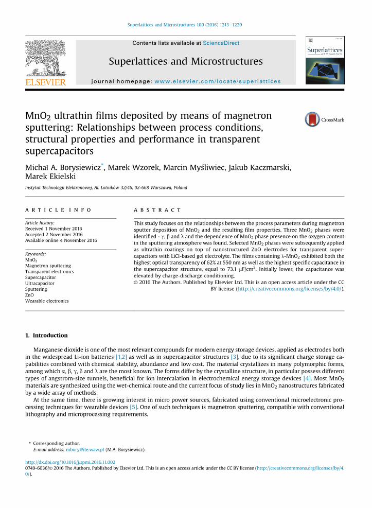
Fig. 1. MnO2 deposition rate as a function of total gas pressure for three oxygen flows: 0, 1 and 5 sccm, derived using XRR.
M.A. Borysiewicz et al. / Superlattices and Microstructures 100 (2016) 1213e1220 1215
3. Results and discussion
3.1. Film characterization
The first important consideration with MnO2 deposition by RF-sputtering is the very low deposition rate (see Fig. 1)compared with e.g. ZnO, averaging 0.28 Å/s in the same reactor and magnetron configuration under high oxygen content (10sccm Ar, 5 sccm O2, 0.8 Pa) and the same RF power of 125W. However low, the deposition rate drops with both the increase inoxygen flow and total gas pressure as is normally expected during reactive magnetron sputtering.
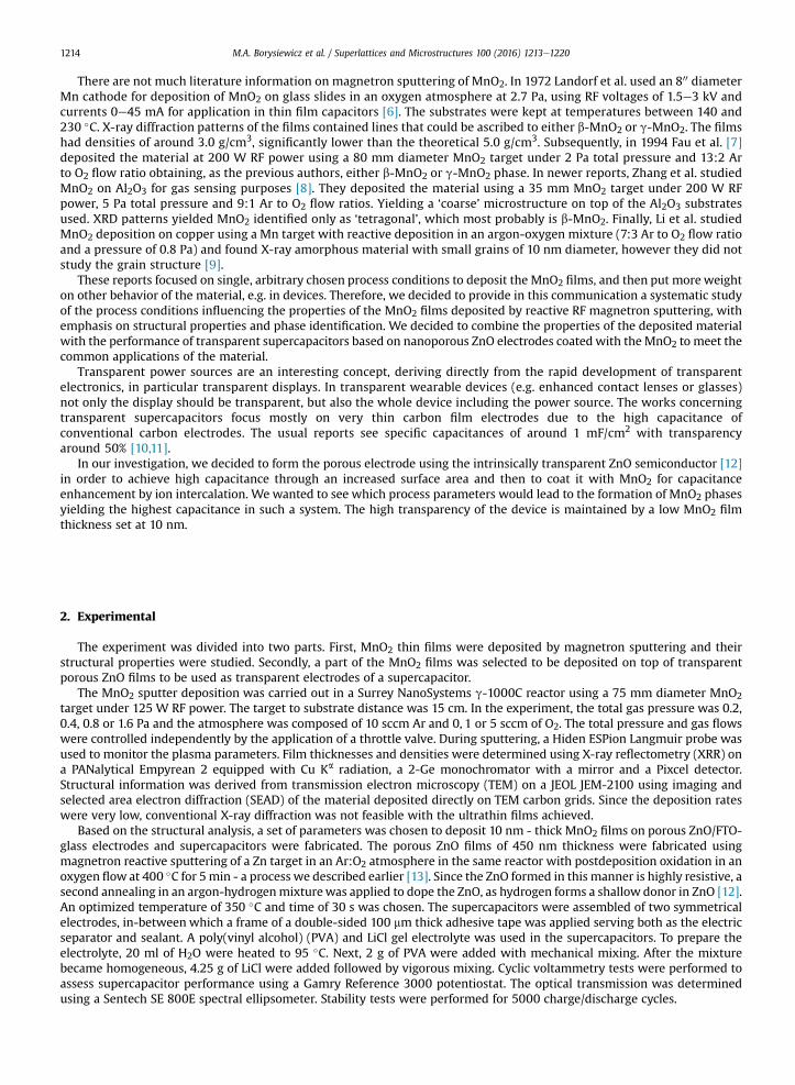
As shown in Fig. 2, the plasma electron temperature and density determined from Langmuir probe measurementsexhibited changes within ranges typical for oxide sputtering on this magnetron (Te ¼ 2.0e3.0 eV andNe ¼ 1017e1.6$1017 cm�3). Te values are the highest for 0.2 Pa and drop with increasing pressure, although at 0.4e1.6 Pa, thevalues change only very little. Also, apart from the data at 0.2 Pa, there is little difference between Te for different oxygen flowsat the respective pressures. Similarly, the Ne is the lowest at 0.2 Pa and then it rises, but flattens out for the higher pressures.Here, the differences between the data points for each pressure are larger, but still the whole behavior can be described asalmost stable. No correlation can be seen between the plasma parameters and deposition rate.
By analyzing the radial intensities of electron diffraction patterns (see Fig. 3a and b) wewere able to distinguish three pairsof lines, always appearing together in the patterns. They are related to the following d-spacings: 2.45 Å and 1.39 Å, 2.13 Å and1.62 Å as well as 2.00 Å and 1.54 Å. We cross-checked the PDF-2 database for possible matches, in particular against MnO (01-071-4748), Mn3O4 (00-024-0734) and Mn2O3 (03-065-7467) but found no positive correlations for both lines in each pair. Wewere however able to ascribe the peaks positively to different MnO2 phases, based on experimental data for nanoparticles byDevaraj et al. [4]. We found therefore, that based on experimental conditions, we were able to fabricate a mixture of threeMnO2 phases: g (2.45 Å and 1.39 Å), b (2.13 Å and 1.62 Å) and l (2.00 Å and 1.54 Å). The respective planes are noted in Fig. 3b. Amatrix of the observed MnO2 phases as a function of both oxygen flow and total pressure was created and is presented inFig. 3c. It is visible, that g-MnO2 is always present, independently on the process parameters. The samples deposited at 1.6 Paand both 1 and 5 sccm O2 exhibit only g-MnO2 lines. However, the strongest intensity of the g-MnO2 lines was observed forthe film deposited at 0.8 Pa and 1 sccm O2.With decreasing pressure and oxygen flowewhich can be interpreted as generallydecreasing oxygen content in the sputtering chamber e b-MnO2 starts to appear in the samples with its strongest peaksvisible for 1 sccm O2 and total pressures from 0.2 to 0.8 Pa. Then for 0 sccm oxygen the l phase is present for all total gaspressures and the peaks related to this phase appear to be relatively constant as a function of the pressure.
TEM images taken for the samples show two main crystallite types. Small, agglomerated almost circular ones with anapproximated radius of several nm (see Fig. 4a) and long needle-like (see Fig. 4b and c). Looking at high magnification imagesit can be seen, that the ‘needles’ are actually more like bent petals with a significant portion laying on the surface and oneedge sticking out of the sample plane, creating the needle-type image (see Fig. 4d). By selected area FFT e inverse FFT se-lection and analysis, we were able to obtain clear images of the crystalline planes and determined the interplanar spacings ofthe visible crystallites. Both types were found to be g-MnO2, the dominant phase in the samples. Furthermore, the medianround crystallite sizewas found to fall with the increasing oxygen flow, with 31e80 nm2 for 0 sccm, 31e49 nm2 for 1 sccm and4e19 nm2 for 5 sccm. The needle/petal crystallite density is also not uniformwith regard to process conditions. Their presenceis higher for the 5 sccm O2 samples than 1 sccm O2 ones, with their highest density for the 0.8 Pa pressure in both cases. Thedensity drops with the increasing oxygen content as defined previously for beMnO2with no such crystallites visible either in
Fig. 2. Electron temperature (a) and electron density (b) derived from Langmuir probe I-V measurements of the plasma discharge during MnO2 target sputtering,as a function of total gas pressure for three oxygen flows: 0, 1 and 5 sccm.
M.A. Borysiewicz et al. / Superlattices and Microstructures 100 (2016) 1213e12201216
the sample 1 sccm O2/0.2 Pa nor in any of the samples for 0 sccm O2. We were not able to physically identify the crystals ofother phases, but this might be due to the overlap of the different crystallites in the specimens used. One may hypothesize,that due to the low thickness of the samples the other crystallites should be very small and would require a higher resolutionmicroscope for a full analysis. However, the captured SAED patterns prove their presence in the samples.
The density of the films was determined using XRR and the results are shown in Fig. 5. The higher the oxygen flow duringthe experiment, the lower the material density. Taking into consideration the samples grown at 0.8 Pa, for 0 sccm O2 thedensity is 5.6 g cm�3, for 1 sccm O2 it is 4.8 g cm�3 and finally for 5 sccm e 4.6 g cm�3. The trends show a slight drop withdecreasing pressure and a rise with increasing pressure. These results are far from the 5.0 g cm�3 bulk MnO2 density andrelate more to the densities of MnO (5.43 g cm�3), Mn3O4 (4.86 g cm�3) and Mn2O3 (4.5 g cm�3). Here the samples arehowever in the form of thin films or rather collections of nanoparticle grains, which also are not completely continuous asseen from TEM images. Although the density of different MnO2 phases are not well referenced in the literature, an exampleconcerning a-MnO2 density of 4.21 g cm�3 can be found [14] or l-MnO2 density of 4.48e4.61 g cm�3 [15] showing significantdifference from the theoretical 5.0 g cm�3. Taking this into account, the measured densities of the samples can serve asreference.
3.2. Supercapacitor performance
Based on the material characterization data gathered, we chose 5 process parameter sets for the fabrication of 10 nm thickMnO2 films on sputter deposited nanocrystalline ZnO [13] for application as transparent electrodes in supercapacitors. Wechose three samples deposited at 0.8 Pa and 0, 1 and 5 sccm O2 and the samples grown at 1 sccm O2 and 0.2 Pa and 1.6 Pa to
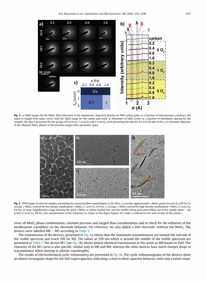
Fig. 3. a) SAED images for the MnO2 films fabricated in the experiment, deposited directly on TEM carbon grids, as a function of total pressure (columns) andargon to oxygen flow ratios (rows) with the SAED image for the carbon grid itself; b) Intensities of SAED circles as a function of interplanar spacing for thesamples, the data is presented for the groups of 0 sccm O2, 1 sccm O2 and 5 sccm O2, each presenting the data for 0.2, 0.4, 0.8 and 1.6 Pa; c) a schematic depictionof the obtained MnO2 phases in the pressure-oxygen flow parameter space.
Fig. 4. TEM images of selected samples presenting the nanocrystalline morphologies in the films: a) circular, agglomerated g-MnO2 grains (0 sccm O2, 0.8 Pa); b)circular g-MnO2 covered by low density needle/petal g-MnO2 (1 sccm O2, 0.4 Pa); c) circular g-MnO2 covered by high density needle/petal g-MnO2 (5 sccm O2,0.4 Pa); d) large magnification image showing the petal g-MnO2 in yellow dashed line, and the needles being petal parts folded out of the sample plane e redarrow (5 sccm O2, 0.8 Pa). (For interpretation of the references to colour in this figure legend, the reader is referred to the web version of this article.)
M.A. Borysiewicz et al. / Superlattices and Microstructures 100 (2016) 1213e1220 1217
cover all MnO2 phase combinations, constant pressure and oxygen flow considerations and to check for the influence of theneedle/petal crystallites on the electrode behavior. For reference, we also added a ZnO electrode, without the MnO2. Thedevices were labelled M0 e M5 according to Table 1.
The transmission of the devices, presented in Fig. 6a shows that the maximum transmittances are toward the red end ofthe visible spectrum and reach 70% for M2. The values at 550 nm which is around the middle of the visible spectrum arepresented in Table 1. The device M1 (see Fig. 6b) shows almost identical transmission at this point as M0 based on ZnO. Thecharacter of the M1 curve is also specific, similar only to M0 and M4, whereas the other devices have much sharper drops intransmittance when moving to shorter wavelengths.
The results of electrochemical cyclic voltammetry are presented in Fig. 6c. The cyclic voltammograms of the devices showan almost rectangular shape for the ZnO supercapacitor, indicating a close to ideal capacitor behavior, with only aminor slope,
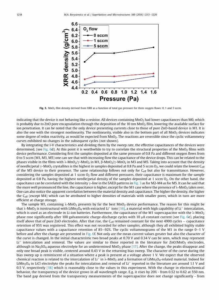
Fig. 5. MnO2 film density derived from XRR as a function of total gas pressure for three oxygen flows: 0, 1 and 5 sccm.
M.A. Borysiewicz et al. / Superlattices and Microstructures 100 (2016) 1213e12201218
indicating that the device is not behaving like a resistor. All devices containing MnO2 had lower capacitances than M0, whichis probably due to ZnO pore encapsulation through the deposition of the 10 nmMnO2 film, lowering the available surface forion penetration. It can be noted that the only device presenting currents close to those of pure ZnO-based device is M1. It isalso the one with the strongest nonlinearity. The nonlinearity, visible also in the bottom part of all MnO2 devices indicatessome degree of redox reactivity, as would be expected from MnO2. The reactions are reversible since the cyclic voltammetrycurves exhibited no changes in the subsequent cycles (not shown).
By integrating the I-V characteristics and dividing them by the sweep rate, the effective capacitances of the devices weredetermined, (see Fig. 6d). At this point it is worthwhile to try to correlate the structural properties of the MnO2 films withdevice performance. Considering first the samples deposited at the same pressure of 0.8 Pa and different oxygen flows from0 to 5 sccm (M1, M3, M5) one can see that with increasing flow the capacitance of the device drops. This can be related to thephases visible in the films with l-MnO2/g-MnO2 in M1, b-MnO2/g-MnO2 in M3 and M5. Taking into account that the densityof needle/petal g-MnO2 crystallites is the highest in samples deposited at 0.8 Pa and 5 sccm O2, we could relate the lowest Ceffof the M5 device to their presence. The same relationship follows not only for Ceff but also for transmittance. However,considering the samples deposited at 1 sccm O2 flow and different pressures, their capacitance is maximum for the sampledeposited at 0.8 Pa, having the highest needle/petal density of the samples deposited at 1 sccm O2. On the other hand, thecapacitance can be correlatedwith the intensity g-line in the SAED patterns in Fig. 3 as for M2-M4 as for M5. It can be said thatthemorewell pronounced the line, the capacitance is higher, except for theM1 casewhere the presence of l-MnO2 takes over.One can also notice the apparent correlation between thematerial density and capacitance. The higher the density, the higherthe Ceff (except M4) which can be attributed to higher densities of materials with smaller pores, which in turn are moreefficient at charge storage.
The sample M1, containing l-MnO2 presents by far the best MnO2 device performance. The reason for this might bethat l-MnO2 is isostructural with LiMn2O4 with extracted Liþ ions [16], a material with high capability of Liþ intercalation,which is used as an electrode in Li-ion batteries. Furthermore, the capacitance of the M1 supercapacitor with the l-MnO2phase rose significantly after 100 galvanostatic charge-discharge cycles with 10 mA constant current (see Fig. 6e), placingitself above that of pure ZnO electrodes. After that rise, the Ceff remained constant for the next 4900 cycles e capacitanceretention of 95% was registered. This effect was not recorded for other samples, although they all exhibited highly stablecapacitance values with a capacitance retention of 85e92%. The cyclic voltammograms of the M1 in the range 0e1 Vbefore and after the change are presented in Fig. 6f. Not only are the mean current values greater but also the character ofthe curve is changed. In the initial characteristic two broad peaks at 0.70 V and 0.34 V can be seen, which may representLiþ intercalation and removal. The values are similar to those reported in the literature for ZnO/MnO2 electrodes,although in Na2SO4 aqueous electrolyte for an undetermined MnO2 phase [17]. After the change, the peaks disappear andonly one broad peak is visible, centered around 0.43 V in the returning bias sweep. The character of the curve during thebias sweep up is reminiscent of a situation where a peak is present at a voltage above 1 V. We expect that the observedchemical reaction is related to the intercalation of Liþ in l-MnO2 and a formation of LiMn2O4-related material. Indeed forLiMn2O4 in LiCl electrolyte the peaks for intercalation and removal of Liþ reported in the literature are around 1.1 V and0.5 V, respectively [18] which is reasonably close to the values in this experiment. With the change in electrochemicalbehavior, the transparency of the device grows in all wavelength range. E.g. it rises by 20% - from 0.52 to 0.62 at 550 nm.The band gap derived from the transparency measurements of the supercapacitor does not change significantly - from
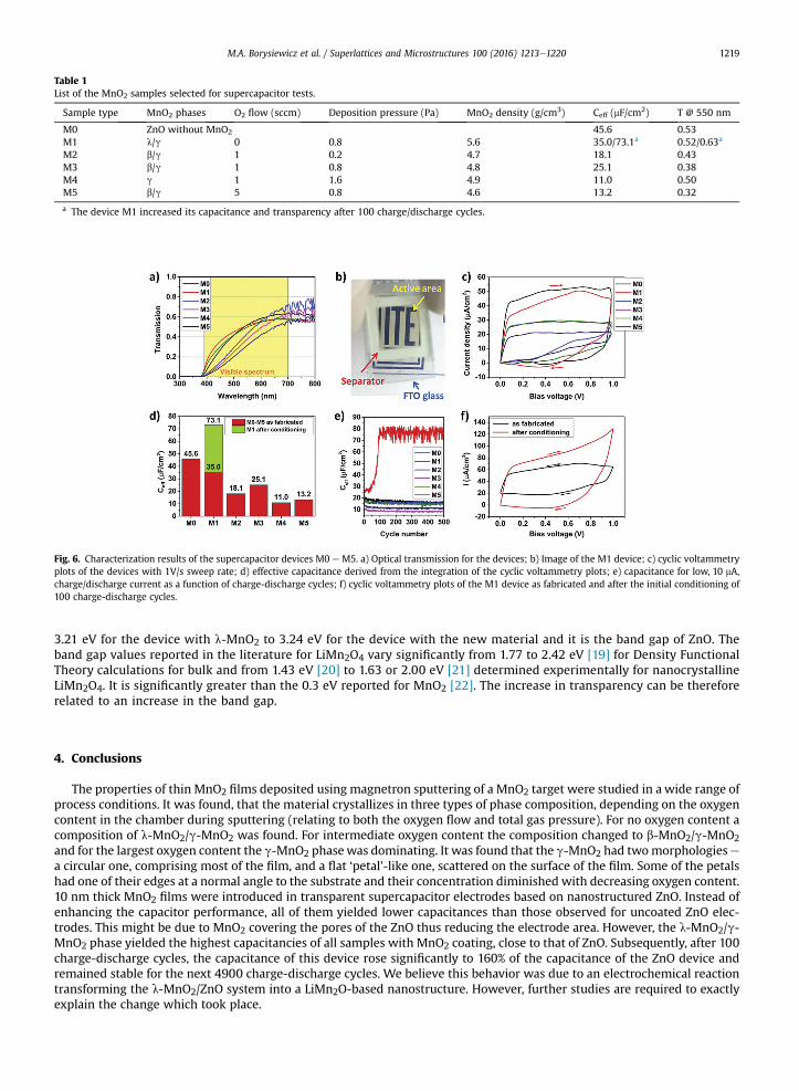
Table 1List of the MnO2 samples selected for supercapacitor tests.
Sample type MnO2 phases O2 flow (sccm) Deposition pressure (Pa) MnO2 density (g/cm3) Ceff (mF/cm2) T @ 550 nm
M0 ZnO without MnO2 45.6 0.53M1 l/g 0 0.8 5.6 35.0/73.1a 0.52/0.63a
M2 b/g 1 0.2 4.7 18.1 0.43M3 b/g 1 0.8 4.8 25.1 0.38M4 g 1 1.6 4.9 11.0 0.50M5 b/g 5 0.8 4.6 13.2 0.32
a The device M1 increased its capacitance and transparency after 100 charge/discharge cycles.
Fig. 6. Characterization results of the supercapacitor devices M0 e M5. a) Optical transmission for the devices; b) Image of the M1 device; c) cyclic voltammetryplots of the devices with 1V/s sweep rate; d) effective capacitance derived from the integration of the cyclic voltammetry plots; e) capacitance for low, 10 mA,charge/discharge current as a function of charge-discharge cycles; f) cyclic voltammetry plots of the M1 device as fabricated and after the initial conditioning of100 charge-discharge cycles.
M.A. Borysiewicz et al. / Superlattices and Microstructures 100 (2016) 1213e1220 1219
3.21 eV for the device with l-MnO2 to 3.24 eV for the device with the new material and it is the band gap of ZnO. Theband gap values reported in the literature for LiMn2O4 vary significantly from 1.77 to 2.42 eV [19] for Density FunctionalTheory calculations for bulk and from 1.43 eV [20] to 1.63 or 2.00 eV [21] determined experimentally for nanocrystallineLiMn2O4. It is significantly greater than the 0.3 eV reported for MnO2 [22]. The increase in transparency can be thereforerelated to an increase in the band gap.
4. Conclusions
The properties of thin MnO2 films deposited using magnetron sputtering of a MnO2 target were studied in a wide range ofprocess conditions. It was found, that the material crystallizes in three types of phase composition, depending on the oxygencontent in the chamber during sputtering (relating to both the oxygen flow and total gas pressure). For no oxygen content acomposition of l-MnO2/g-MnO2 was found. For intermediate oxygen content the composition changed to b-MnO2/g-MnO2and for the largest oxygen content the g-MnO2 phasewas dominating. It was found that the g-MnO2 had twomorphologiesea circular one, comprising most of the film, and a flat ‘petal’-like one, scattered on the surface of the film. Some of the petalshad one of their edges at a normal angle to the substrate and their concentration diminished with decreasing oxygen content.10 nm thick MnO2 films were introduced in transparent supercapacitor electrodes based on nanostructured ZnO. Instead ofenhancing the capacitor performance, all of them yielded lower capacitances than those observed for uncoated ZnO elec-trodes. This might be due to MnO2 covering the pores of the ZnO thus reducing the electrode area. However, the l-MnO2/g-MnO2 phase yielded the highest capacitancies of all samples with MnO2 coating, close to that of ZnO. Subsequently, after 100charge-discharge cycles, the capacitance of this device rose significantly to 160% of the capacitance of the ZnO device andremained stable for the next 4900 charge-discharge cycles. We believe this behavior was due to an electrochemical reactiontransforming the l-MnO2/ZnO system into a LiMn2O-based nanostructure. However, further studies are required to exactlyexplain the change which took place.

M.A. Borysiewicz et al. / Superlattices and Microstructures 100 (2016) 1213e12201220
Acknowledgments
This work was carried out in the frames of the NACZO project [23], supported by the Polish National Centre for Researchand Development (NCBiR) under Grant No. LIDER/030/615/L-5/NCBR/2014.
References
[1] X. Guo, J. Han, L. Zhang, P. Liu, A. Hirata, L. Chen, T. Fujita, M. Chen, Nanoscale 7 (2015) 15111e15116, http://dx.doi.org/10.1039/C5NR05011A.[2] S. Deng, L. Wang, T. Hou, Y. Li, J. Phys. Chem. C 119 (2015) 28783e28788, http://dx.doi.org/10.1021/acs.jpcc.5b10354.[3] M. Huang, F. Li, F. Dong, Y.X. Zhang, L.L. Zhang, J. Mater. Chem. A 3 (2015) 21380e21423, http://dx.doi.org/10.1039/C5TA05523G.[4] S. Devaraj, N. Munichandraiah, J. Phys. Chem. C 112 (2008) 4407e4417, http://dx.doi.org/10.1021/jp7108785.[5] S. Ferrari, M. Loveridge, S.D. Beattie, M. Jahn, R.J. Dashwood, R. Bhagat, J. Power Sources 286 (2015) 25e46, http://dx.doi.org/10.1016/j.jpowsour.2015.
03.133.[6] R.W. Landorf, S.J. Licht, J. Electrochem. Soc. 119 (1972) 430e433, http://dx.doi.org/10.1149/1.2404223.[7] P. Fau, J.P. Bonino, A. Rousset, Appl. Surf. Sci. 78 (1994) 203e210, http://dx.doi.org/10.1016/0169-4332(94)00111-1.[8] C. Zhang, A. Boudiba, C. Navio, M.-G. Olivier, R. Snyders, M. Debliquy, Sensors Actuators B 161 (2012) 914e922, http://dx.doi.org/10.1016/j.snb.2011.11.
062.[9] Y. Li, H. Xie, J. Li, J. Wang, Mater. Lett. 102e103 (2013) 30e32, http://dx.doi.org/10.1016/j.matlet.2013.03.098.
[10] K. Gao, Z. Shao, X. Wu, X. Wang, Y. Zhang, W. Wang, F. Wang, Nanoscale 5 (2013) 5307e5311, http://dx.doi.org/10.1039/C3NR00674C.[11] J. Ge, G. Cheng, L. Chen, Nanoscale 3 (2011) 3084e3088, http://dx.doi.org/10.1039/C1NR10424A.[12] A. Janotti, C.G. van de Walle, Rep. Prog. Phys. 72 (2009) 126501, http://dx.doi.org/10.1088/0034-4885/72/12/126501.[13] M.A. Borysiewicz, E. Dynowska, V. Kolkovsky, J. Dyczewski, M. Wielgus, E. Kami�nska, A. Piotrowska, Phys. Stat. Sol. A 209 (2012) 2463e2469, http://dx.
doi.org/10.1002/pssa.201228041.[14] Dale L. Perry, Handbook of Inorganic Compounds, second ed., CRC Press, 2011. ISBN 9781439814611.[15] W.L. Bowden, K. Brandt, P.A. Christian, Z. Jiang, United States Patent 6,759,167, July 6, 2004.[16] Helena Berg, Håkan Rundl€ov, John O. Thomas, Solid State Ionics 144 (2001) 65e69, http://dx.doi.org/10.1016/S0167-2738(01)00894-3.[17] P. Yang, X. Xiao, Y. Li, Y. Ding, P. Qiang, X. Tan, W. Mai, Z. Lin, W. Wu, T. Li, H. Jin, P. Liu, J. Zhou, C. Ping Wong, Z.L. Wang, ACS Nano 7 (2013) 2617e2626,
http://dx.doi.org/10.1021/nn306044d.[18] M. Jayalakshmi, M. Mohan Rao, F. Scholz, Langmuir 19 (2003) 8403e8408.[19] K. Hoang, arXiv: 1412.5264v1 [cond-mat.mtrl-sci] 17 Dec 2014.[20] M. Raja, S. Mahanty, P. Ghosh, R. Basu, H. Maiti, Mater. Res. Bull. 42 (2007) 1499e1506.[21] K. Kushida, K. Kuriyama, Appl. Phys. Lett. 77 (2000) 4154e4156.[22] A.K.M. Farid ul Islam, R. Islam, K.A. Khan, J. Mater. Sci. Mater. Electron 16 (2005) 203e207.[23] http://www.naczo.ite.waw.pl.
Related Documents