Noname manuscript No. (will be inserted by the editor) Superconducting Phase Qubits John M. Martinis Received: date / Accepted: date Abstract Experimental progress is reviewed for superconducting phase qubit research at the University of California, Santa Barbara. The phase qubit has a potential ad- vantage of scalability, based on the low impedance of the device and the ability to microfabricate complex “quantum integrated circuits”. Single and coupled qubit ex- periments, including qubits coupled to resonators, are reviewed along with a discus- sion of the strategy leading to these experiments. All currently known sources of qubit decoherence are summarized, including energy decay (T 1 ), dephasing (T 2 ), and mea- surement errors. A detailed description is given for our fabrication process and control electronics, which is directly scalable. With the demonstration of the basic operations needed for quantum computation, more complex algorithms are now within reach. Keywords quantum computation · qubits · superconductivity · decoherence 1 Introduction Superconducting qubits are a unique and interesting approach to quantum computation because they naturally allow strong coupling. Compared to other qubit implementa- tions, they are physically large, from ∼ 1 μm to ∼ 100 μm in size, with interconnection topology and strength set by simple circuit wiring. Superconducting qubits have the advantage of scalability, as complex circuits can be constructed using well established integrated-circuit microfabrication technology. A key component of superconducting qubits is the Josephson junction, which can be thought of as an inductor with strong non-linearity and negligible energy loss. Combined with a capacitance, coming from the tunnel junction itself or an external element, a inductor-capacitor resonator is formed that exhibits non-linearity even at the single photon level. As shown in Fig. 1, the two lowest quantum eigenstates of this non-linear resonator can then be identified as the qubit states |0i and |1i. John M. Martinis University of California, Santa Barbara Santa Barbara, Ca 93106 Tel.: 805-893-3910 E-mail: [email protected]

Welcome message from author
This document is posted to help you gain knowledge. Please leave a comment to let me know what you think about it! Share it to your friends and learn new things together.
Transcript

Noname manuscript No.(will be inserted by the editor)
Superconducting Phase Qubits
John M. Martinis
Received: date / Accepted: date
Abstract Experimental progress is reviewed for superconducting phase qubit research
at the University of California, Santa Barbara. The phase qubit has a potential ad-
vantage of scalability, based on the low impedance of the device and the ability to
microfabricate complex “quantum integrated circuits”. Single and coupled qubit ex-
periments, including qubits coupled to resonators, are reviewed along with a discus-
sion of the strategy leading to these experiments. All currently known sources of qubit
decoherence are summarized, including energy decay (T1), dephasing (T2), and mea-
surement errors. A detailed description is given for our fabrication process and control
electronics, which is directly scalable. With the demonstration of the basic operations
needed for quantum computation, more complex algorithms are now within reach.
Keywords quantum computation · qubits · superconductivity · decoherence
1 Introduction
Superconducting qubits are a unique and interesting approach to quantum computation
because they naturally allow strong coupling. Compared to other qubit implementa-
tions, they are physically large, from ∼ 1 µm to ∼ 100 µm in size, with interconnection
topology and strength set by simple circuit wiring. Superconducting qubits have the
advantage of scalability, as complex circuits can be constructed using well established
integrated-circuit microfabrication technology.
A key component of superconducting qubits is the Josephson junction, which can
be thought of as an inductor with strong non-linearity and negligible energy loss.
Combined with a capacitance, coming from the tunnel junction itself or an external
element, a inductor-capacitor resonator is formed that exhibits non-linearity even at
the single photon level. As shown in Fig. 1, the two lowest quantum eigenstates of this
non-linear resonator can then be identified as the qubit states |0〉 and |1〉.
John M. MartinisUniversity of California, Santa BarbaraSanta Barbara, Ca 93106Tel.: 805-893-3910E-mail: [email protected]

2
0.5 1 1.5 20
0.2
0.4
0.6
0.8
1
|0
|1
Pulse height Imeas [a.u.]
Pro
ba
bili
ty to
tu
nn
el
|0>|1>
96%
a operate
U( )
Iµw
ImeasIdc
measureb
c
Fig. 1 (a) Plot of non-linear potential U(δ) for the Josephson phase qubit. The qubit states|0〉 and |1〉 are the two lowest eigenstates in the well. The junction bias Idc is typically chosento give 3-7 states in the well. Microwave current Iµw produces transitions between the qubitstates. (b) Plot of potential during state measurement. The well barrier is lowered with a biaspulse Imeas so that the |1〉 state can rapidly tunnel. (c) Plot of tunneling probability versusImeas for the states |0〉 and |1〉. The arrow indicates the optimal height of Imeas, which givesa fidelity of measurement close to the maximum theoretical value 96%.
The junction non-linearity can be expressed in circuits by different ways, leading
to qubit types that have been named [1] charge, flux, transmon [2], and phase qubits.
As discussed in a previous review article [1], each type has certain advantages and
disadvantages. At UC Santa Barbara, we have focussed on the phase qubit because it
has the largest capacitance and consequently has a characteristic resonator impedance
close to 50Ω. This is a convenient impedance since microwave circuits are typically
designed for 50Ω, and impedance matching implies that phase qubits can be strongly
coupled to transmission lines and resonator circuits. Similarly, phase qubits can be
directly wired together over relatively long distances, since the stray capacitance of
the wires can be made negligible compared to the junction capacitance. Although
impedance has not been a critical issue for present proof-of-principle experiments,
we believe this circuit property may become increasingly important as more complex
integrated circuits are realized.
Note that these same wires that permit scaling to large qubit architectures also
allow qubits to interact with unwanted defects and electromagnetic modes, increasing
the possibility for dissipation and decoherence. Understanding decoherence is thus a
critical issue for all superconducting qubits, and will be specifically addressed in this
review.
This article is not intended to be a comprehensive explanation of phase qubits,
but more a guide to publications by the Santa Barbara group in the last few years.
I will mostly review the strategy, concepts, and implications of these experiments.
In addition, some important details have been left out of prior publications, notably
fabrication and control electronics, and this review will be used to more fully docu-
ment these issues. Since many of the experiments demonstrated advances in several
areas, the review will be structured along topics, listing chronologically the important
developments when appropriate.
2 Single Qubits
Superconducting qubit research began in the 1980’s motivated by the question, posed
by Anthony Leggett, whether macroscopic variables would behave in a quantum me-

3
chanical fashion [3]. Initial experiments verified quantum behavior via the phenomenon
of tunneling out of the zero-voltage state of a current-biased Josephson junction [4]. At
UC Berkeley, quantum mechanical behavior was also demonstrated by the existance
of quantized energy levels [5]. This observation provided stronger proof of quantum
behavior, and established at an early stage (before the ideas of qubits were even widely
established) that superconducting circuits could be used as general quantum systems
[6].
Motivated by theoretical developments in quantum computing, research into phase
qubits was renewed in the early 2000’s. The University of Maryland group proposed in
2001 that qubits could be encoded as the ground and first excited state of a current-
biased Josephson junction [7]. The phase qubit was first demonstrated at NIST in
2002 with an experiment [8] that performed all of the basic operations needed for a
single qubit: initialization of the qubit state, coherent Rabi oscillations, and a proba-
bilistic single-shot measurement of the final state. An important conceptual advance
in this circuit was biasing the junction with a magnetic flux applied to superconduct-
ing loop, which provided a large impedance transformation that isolated the qubit
from the strongly dissipative 50Ω impedance of the bias leads. Another advance was
measurement, which was performed by first driving a transition from |1〉 to a higher
energy eigenstate, which would then rapidly tunnel out of the well to produce an easily
measured voltage signal.
This initial experiment obtained a coherence time of approximately 20 ns, a value
much smaller than ∼ 4 µs expected from damping of the bias leads. To probe the
cause of this discrepancy, the fabrication procedure was first changed, replacing the
Nb superconductor with Al, since long ∼ 1 µs coherence times had been already been
achieved [9] with charge qubits using Al. This change in materials did not improve the
qubit coherence, so we next investigated the role of quasiparticles that were generated
in the junction when switching into the voltage state [10]. Because the qubit escape rate
was found to be influenced by changes to the generation and decay of quasiparticles, the
qubit design was more radically modified so that quasiparticles would not be produced
by the qubit junction during measurement [11].
All subsequent qubits are based on this new design, which is shown in Fig. 2 for our
current layout. The qubit junction is still biased through a superconducing loop, but
now the tunneling event simply changes the circulating current in the loop. This current
change is read out with a separate SQUID magnetometer that is connected only by
flux, electrically isolating the qubit junction from the readout so that any quasiparticles
generated in the readout cannot diffuse into the qubit junction. In addition, an external
shunt resistor is also connected across the SQUID so that it switches to about 1/4-th the
gap voltage [10]. This minimizes the generation of quasiparticles, and ensures that the
Josephson oscillations have a frequency smaller than the gap so that no quasiparticles
can be excited in the qubit loop. Using this new design, we have not seen any effects
of quasiparticle heating, validating the design change. Also note that a gradiometer
design is currently used for both the qubit and readout SQUID to minimize flux offsets
from trapped magnetic flux in the ground plane.
With this new design, the qubit coherence time was unchanged. Careful spec-
troscopy sweeps in bias were performed for the first time, which showed structures
corresponding to avoided level crossings [11]. These “spurious resonances” were shown
to be consistent with a model of the qubit interacting with two-level states (TLS) pro-
duced by atoms in the dielectric tunneling between two sites [12] (or more generally
the tunneling between two configurations of atoms.) Although these resonances were
4
SQUID readoutmeasurepulse
qubitjunction
qubitcapacitor
qubitinductor
flux bias
SQUIDreadout
astate
controlqubitbias
qubit
Cs I0
25 mK
L
50 m
20dB
20dB
20dB
20dB RC RCRC
4 K
CPCP
5 H
0.5 fF
Isq VsqImeasIdcIµw
b
50
1 pF
100
chip
Fig. 2 (a) Schematic diagram of a phase qubit circuit and bias lines. Symbols 20 dB, RC,and CP represent 20 dB microwave attenuators, resistor-capacitor low-pass filters, and copper-powder microwave filters, respectively. The RC filters for the qubit and SQUID bias has 1 kΩand 10 kΩ DC resistance, respectively, and a roll-off frequency ∼ 5 MHz. The 5 µH inductoris a custom made radio-frequency bias tee with no transmitting resonances below 1GHz. (b)Photomicrograph of present phase qubit, showing small area (∼ 1 µm2) junction shunted bya parallel plate capacitor. Microwave drive line (with capacitor, not shown) comes from theleft. The qubit inductor is coupled to a SQUID readout circuit in a gradiometer geometry. Theflux bias lines for the qubit are symmetrically placed about the SQUID and counter-wound toinhibit flux coupling to the SQUID. The SQUID bias line exits to the right. The holes in theground plane inhibit trapped vortices in the superconducting ground plane.
initially hypothesized to fluctuate the critical current, it was later proposed [13] and
demonstrated [14] that they instead produce a fluctuation in charge.
In the next publication [15], we improved state measurement by applying a ∼ 3 ns
pulse to the qubit bias line, causing the |1〉 state to directly tunnel, as illustrated in
Fig. 1(b). With faster measurement, we were then able to show that the qubit |1〉state, when biased on resonance with the two-level fluctuator, could Rabi swap the
excited photon. The magnitudes and density of these TLS fluctuators were also shown
to explain why the measurement probabilities of Rabi oscillations were about 1/2 the
expected magnitude.
The breakthrough in phase qubit coherence came in 2005 [14], when we first identi-
fied the source of the spurious resonators to be two-level states (TLS) in the dielectrics
(insulators) of the device. With conventional inductor-capacitor resonators, we first
showed that a common dielectric used in superconducting devices, amorphous a-SiO2,
had a large intrinsic dielectric loss tangent δi ' 0.005. This loss was shown to de-
crease at high power or temperature because of saturation effects. We then showed
that the spurious resonances have a distribution of splitting sizes, as measured with
qubit spectroscopy, consistent with individual TLS in the AlOx dielectric of the tunnel
junction. The density of splittings were calculated to give AlOx an intrinsic loss tan-
gent 0.0016, close to the a-SiO2 value. We also demonstrated that the splitting density
increases with junction area, and argued that large area junctions (A > 100 µm2) have
enough overlapping splittings so that this loss tangent directly determines the energy
loss time. This calculated time T1 = 8ns correctly predicts what was found in previous
experiments on large area qubits. For small area junctions (A < 1 µm2), much longer
coherence times are observed because the qubit bias can be chosen to statistically avoid
the splittings. Charge and flux qubits must use small area junctions, which explains
why this phenomenon was not originally seen in those devices. This paper also reported

5
that the loss tangent of a-SiNx is about 20 times better than a-SiO2. Replacing the
crossover dielectric with a-SiNx improved the qubit decay time for Rabi oscillations to
500 ns.
We note that this dramatic increase in T1 came from a number of device improve-
ments. Most importantly, the junction area was reduced and low-loss dielectrics were
used in the wiring crossovers. We also switched substrates from silicon to sapphire, since
we found that resonators made on silicon with CVD-deposited a-SiO2 and a-SiNx di-
electrics had anomalously high dissipation. This presumably comes from a conducting
2-dimensional electron gas layer at the surface of the silicon, induced by a large electric
field generated by charge defects in the amorphous dielectric. We have not checked
whether the redesign of the qubit to reduce quasiparticle heating, or the use of Al
instead of Nb, were ultimately important changes.
Although T1 had improved, the amplitude of the Rabi oscillations was at this time
only about 65%. Theory predicted that this measurement fidelity could be improved by
using a qubit junction with smaller area, reducing the number of TLS resonances that
were swept through during the measurement pulse [15]. A device was then tested [16]
that incorporated small area junctions with A = 1 µm2 and shunted with an external
capacitor in order to keep the qubit frequency constant. Spectroscopy data from this
device showed a dramatic decrease in the number of splittings, with the measurement
visibility jumping to about 85%, as expected. The decay time decreased in this device
to T1 = 110 ns, consistent with the loss tangent of the SiNx shunting capacitor. It is
important to note that even though T1 decreased in this device, the reduction in the
number of TLS splittings made the qubit much easier to precisely control. We were
thus able to perform for the first time a number of important experiments, including
partial measurement [17], quantum-state tomography on single [16] and coupled [18]
qubits, and demonstration of entanglement between two qubits [18].
The coherence time T1 was next improved [19] by replacing the dielectric of the
shunt capacitor with hydrogenated amorphous silicon (a-Si:H), which we had shown in
resonator experiments to have about 8 times lower intrinsic loss than a-SiNx. Various
chemical interactions of a-Si:H with Al makes this material much more difficult to
incorporate into a multi-level process. Initial experiments [19–21] gave T1 = 450 ns,
whereas more recent devices have shown decay times as long as 600 ns. Experiments
are currently underway to optimize the growth of this a-Si:H dielectric.
The best performance of a single qubit is shown in Fig. 3 for Rabi oscillations.
Ramsey fringes (not shown) have given dephasing times as long as 200 ns, although we
typically find T2 = 120 ns for present qubits. A spin-echo sequence [22] has been shown
to increase the dephasing time to about 300 ns.
At this time, a new generation of electronics gave microwave phase control [17],
allowing the qubit state to be rotated around any axis on the equator of the Bloch
sphere. With microwaves applied slightly out of resonance, rotation off-axis from the
equator also became possible. We also improved the flux bias line by DC coupling
the measurement pulse and installing a bias-tee inductor to the (low frequency) DC
bias line. These improvements allowed fast and accurate current pulses to be applied
to the qubit, enabling precise control in time of the qubit frequency, and giving phase
control of the qubit state through rotation around the pole (z-axis) of the Bloch sphere.
Experiments on single qubit tomography demonstrated this Z-gate control [16].

6
0 100 200 300 400 5000
0.2
0.4
0.6
0.8
1
Microwave Pulse Length [ns]
Pro
ba
bili
ty
Rabi Oscillations
measurepulse length
Fig. 3 Measurement of Rabi oscillations. The measurement probability of the |1〉 state isplotted versus microwave pulse length. Pulse sequence consists of a microwave pulse of variabletime, tuned to the qubit transition frequency, followed by a measurement pulse, as depictedin the inset. Note that the probability is the raw data (with no corrections) coming from ourexperiment, which inherently has an absolute calibration. The Rabi oscillations have fidelityof about 90%, a value reasonably close to the theoretical expectation 96% [15]. The energydecay time for this qubit is T1 = 600 ns.
3 Partial Measurement
The phase qubit is typically measured through tunneling of the |1〉 state. Because
the tunneling rate can be electrically adjusted, it is possible to vary the probability
for tunneling, and thus the measurement probability. Such partial measurements [17]
allows one to “look inside” the phenomenon of state collapse in order to understand
the evolution of a quantum state due to the measurement process.
In an ideal quantum measurement, the qubit state is determined without error. The
eigenstates |0〉 or |1〉 are measured always as 0 or 1, respectively. For a superposition
state such as (|0〉+ |1〉)/√2, the measurement probability becomes 0.5.
Errors of a few percent arise in our present method of state measurement [15,20]
because the ratio of the tunneling rates from the |0〉 and |1〉 states is finite, typically
∼ 200. The measurement probabilities from these errors, along with small errors from
the qubit state relaxing to the TLS during the measurement pulse [15], can be corrected
for using calibrations and simple linear algebra [18].
The information available from the result of a partial measurement also produces a
change to the quantum state. For perfect measurement, the qubit state is projected into
a known state. For partial measurement, the state still undergoes coherent evolution
that can be experimentally checked. A good simplification for our system is to assume
that the |0〉 state does not tunnel, but that the |1〉 state can tunnel (be measured) with
a probability p that can be adjusted with the measurement bias pulse, as shown in Fig.
1(c). An initial quantum state ψi then probabilistically evolves to two final states, with

7
states and probabilities given by
ψi = a|0〉+ b|1〉 →
ψt p1 (tunneled)
ψf = (a|0〉+ b√
1− p |1〉)/√N 1− p1 (not tunneled)(1)
where the initial state is normalized |a|2 + |b|2 = 1, the probability for tunneling is
p1 = |b|2p, the state of the system after tunneling is ψt, and N = |a|2 + (1 − p)|b|2is the normalization of the final state ψf when not tunneling. For the case of perfect
measurement (p = 1) the final state collapses to |0〉 when not tunneled, as expected.
For partial measurement, the final state is in a superposition of |0〉 and |1〉, and has
changed by a coherent but non-unitary evolution from ψi to ψf . This state evolution
was verified with a phase qubit, with the final state measured with state tomography
[17].
The non-unitary evolution can also be undone or “uncollapsed” using a second
identical measurement pulse, after first performing a π-rotation to exchange the |0〉and |1〉 state. This operation can be considered as a generalization of spin-echo to non-
unitary operations. An experiment showed that that the original state is accurately
restored after these two partial measurements [23].
4 Coupled Qubits
Qubits need to be coupled together to produce entangled states and to perform com-
plex quantum logic operations. The coupling of two qubits, together with single qubit
operations, allow generation of the CNOT gate, a fundamental operation from which
more complex transformations can be constructed.
Phase qubits have been coupled via a capacitance that allows a photonic excitation
to pass between two qubits. This interaction Hamiltonian is of the form
Hint = g(|10〉〈01|+ |01〉〈10|) , (2)
with a coupling strength g that is proportional to the coupling capacitance. If Hintis turned on for at time t such that gt = π, the initial state |01〉 evolves to the state
−i|10〉; the swapping of the photon along with the −i phase factor suggests naming
this operation i-SWAP.
An initial experiment on capacitively coupled phase qubits [24] focused on the spec-
troscopy of qubits, demonstrating an avoided level crossing with an energy splitting of
2g. Experiments by the NIST and UCSB group focussed on testing the time dynam-
ics of this coupling, as needed for understanding how to make a two-qubit gate. All
experiments to date have used fixed capacitive coupling. Single qubit operations were
performed by having them operate on a time scale much faster than the coupling in-
teraction. Later experiments have effectively turned on and off this coupling by biasing
the qubits into and out of resonance.
Our first experiment demonstrated swapping of a photon between a qubit and
a two-level state [15]. Here, the swapping operation was inferred by measuring the
oscillating probability (in time) of only the qubit. In a second publication [25], we per-
formed this swapping experiment between two phase qubits, simultaneously measuring
the states of both qubits. Simultaneous measurement was a significant advance, since
it allows a unambiguous determination of the time dynamics of the two coupled qubits.
It is challenging to perform, since the capacitive coupling is always on and thus couples
8
the qubits during measurement. This causes the measurement of the |1〉 state in one
qubit to sometimes excite the tunneling of the |0〉 state in the other qubit, producing
measurement error. Guided by simple theory and numerical simulations, we were able
to demonstrate that “measurement cross-talk” could be dramatically reduced by over-
lapping the timing of the two measurement pulses. Further theoretical work was able
to accurately predict the tradeoff between coupling and crosstalk [26].
After improving the coherence time of phase qubits, we were able to more accurately
measure the state transformation for this swapping operation [18]. We first measured
the i phase factor of the i-SWAP gate by exciting one of the qubits, creating the |01〉state, and then allowing the qubits to couple for a time t = π/2g, generating the
entangled state |01〉 − i|10〉)/√2. After then applying a π/2 phase rotation via a Z-
gate to one of the qubits and removing the i phase factor, we obtained an entangled
eigenstate. We confirmed that measurements of both qubit states did not oscillate in
time. A full determination of the entangled state was performed with tomography,
which required applying microwave pulses to each qubit before measurement to change
the measurement basis. The density matrix for the entangled state was found to have
off diagonal elements with an i phase factor, as expected, and with a magnitude nearly
that of the diagonal elements. The fidelity of the density matrix was high enough to
definitively show that the state was entangled.
This experiment with state tomography showed correct state transformation start-
ing with one (important) initial state. In order to demonstrate that the coupling oper-
ation works properly for any initial state, state tomography must be performed over a
number of initial states [21]. This process tomography experiment is currently under-
way at UCSB.
Since the CNOT gate can be constructed from two√
i-SWAP operations, measuring
the fidelity of√
i-SWAP is crucial. We have found that the oscillation amplitude of i-
SWAPs is a powerful method to determine the quality of the coupling operation, much
like the use of Rabi oscillations to determine the quality of single-qubit operations.
In Fig. 4 we show recent results for our coupled qubits, which demonstrate higher
amplitude and longer coherence than given in previous publications.
5 Qubit-Resonator Experiments
Superconducting qubits are electrical resonators with a non-linearity that is strong
enough so that microwaves excite transitions only between the |0〉 and |1〉 states. Res-
onators, built from inductors and capacitors or from standing waves in transmission
lines, are linear oscillators that have eigenstates equally spaced in energy. Transitions
are on-resonance between every adjacent pair of eignestates, yielding dynamical be-
havior much different than for a qubit.
Resonators can be driven or probed with large amplitude signals, and lead to a
number of interesting physical effects and possible applications such as qubit readout.
Resonators are also easier to fabricate than qubits because they do not require Joseph-
son junctions, potentially giving a lower loss circuit that can be used for quantum
memory [21]. The large size of a transmission line resonator may enable their use as a
quantum bus to couple qubits over long distances [27,28].
A phase qubit coupled to a resonator was first demonstrated in the late 1980’s,
when spectroscopy experiments at Saclay showed how the qubit energy levels and their
dissipation rates were modified by the complex impedance of a damped transmission

9
0 100 200 300 400 5000
0.2
0.4
0.6
0.8
1
Measure Delay (ns)
Pro
ba
bili
ty
P10
P01
P11
PABA
B
meas. delay
Measurement delay [ns]
Sta
te p
robabili
ty
Fig. 4 Plot of Rabi swapping between the two-qubit states |10〉 and |01〉, which produces anentangling operation that leads to a CNOT gate. The probability for measuring the |10〉, |01〉,and |11〉 states are given by the closed circles, open circles, and × symbols, respectively. Theexperimental sequence is first a short π pulse to excite |10〉, followed by a delay time wherethe states interact and swap |10〉 ↔ |01〉, and then a final simultaneous measurement of bothqubit states, as depicted in the inset. The probability for |11〉 arises from a crosstalk error inmeasurement, where the tunneling of the |1〉 state in one qubit excites the tunneling of the |0〉state in the other qubit with a probability ∼ 20%. Adding the 20% probability to P10 yieldsa visibility of about 90%, which corresponds to the full measured visibility of single qubits, asseen in Rabi oscillations. We thus expect large visibility for the swapping operation once allmeasurement errors are taken into account.
line [29]. By varying the length of the transmission line, the characteristic time of tun-
neling was also measured [30]. These experiments were the first to demonstrate that
any superconducting qubit could be strongly coupled to a resonator. This is easier
to accomplish, compared to other superconducting qubits, because the characteristic
impedance of phase qubits (∼ 10Ω− 100Ω) is similar to that of transmission line res-
onators (50Ω). In the past few years, charge and transmon qubits coupled to resonators
have demonstrated the “strong-coupling” limit [31].
As for coupled qubits, our experimental strategy has been to measure the dynamics
of the coupling in the time domain. Our first experiment [32] used a device that capac-
itively coupled a qubit to a half-wavelength transmission line resonator. By repeatedly
exciting the qubit to the |1〉 state and transferring the photon into the resonator, Fock
states were sequentially generated in the resonator. This state was then analyzed by
swapping these photons back and forth between the resonator and qubit, with the swap
frequency being shown to be proportional to the square-root of the photon number. In
this initial experiment, Fock states with up to 6 photons were created and analyzed.

10
A second experiment [33] yielded a resonator with a factor of 3 improvement in the
energy decay, yielding a T1 for the resonator of 3 µs. We analyzed the decay rate of
the Fock states and demonstrated the rates scale as the photon number for Fock states
from 1 to 5. The improved coherence time also increased the fidelity of the Fock states
and allowed them to be generated up to photon number 15.
The latest device we have measured has T1 = 5 µs. By generalizing the sequence of
operations sent to the qubit, we have been able to create arbitrary photon states up
to 9 photons [34]. The state now can be fully measured, including phase information
of each Fock state, using Wigner tomography.
These resonator experiments also demonstrate precise quantum control of super-
conducting qubits. They have required the most complex sequences to date, as the
production and detection of a 15-photon Fock state uses 32 pulses, all of which have
to be properly designed, calibrated, and electronically generated.
6 Coherence
Understanding coherence in superconducting qubits is more than reporting the best
values of T1 and T2 that have been achieved. This section will focus on the physical
understanding of decoherence mechanisms, as discovered and explored in a number of
experiments on phase qubits. A systematic picture of decoherence will be presented
that hopefully will be a guide to improving the materials and design of future qubits.
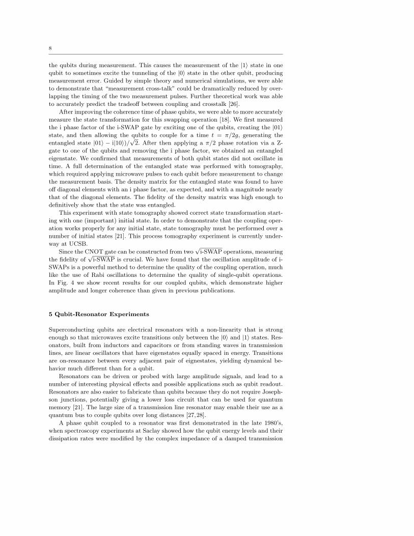
A qubit can be understood as a non-linear resonator made from an inductor and
capacitor [1], as illustrated in Fig. 5. Non-linear inductors are made from Josephson
junctions, and linear inductors from superconducting wires. The capacitor often comes
from the Josephson junction, formed by the overlapping superconducting electrodes
across the thin dielectric of the tunnel barrier, typically a-AlOx. Capacitance may also
come from an external element placed across the junction, deliberately designed into
the device. Additionally, the qubit is also coupled to external electromagnetic modes,
either from various bias lines that are used to control or measure the qubit state, or
inadvertently created, for example, by radiation. Coupling to these external modes is
typically considered as a mechanism for dissipation and energy loss. These three types
of elements form a natural classification of possible decoherence mechanisms.
Energy loss from the inductive elements, including the Josephson junction, is ex-
pected to be very low because the energy gap of the superconducting state provides
no states to which energy can dissipate. Niobium cavity resonators [35], for example,
have been measured to have quality factors Q ∼ 1010. Qubits are typically made using
aluminum, which has a transition temperature Tc ' 1K and an energy gap of about
80GHz. Because the qubit has a frequency typically in the 5 to 20GHz range and
operates at very low temperatures T < Tc/20, no dissipation is expected. An impor-
tant property of superconductors is that the gap is retained even under the presence of
disorder - perfectly so for energy conserving scattering, and with only a small smearing
of the gap for energy loss mechanisms, such as arising from dilute concentrations of
magnetic defects. Even the Josephson effect has a gap protected from such imperfec-
tions [36]. Its non-linear inductance is fundamentally created by Andreev bound states
across the junction. For tunnel junctions with small tunneling matrix elements, these
states retain a gap nearly that of the bulk value. Even for an imperfect junction with
microshorts, giving some conduction channels with large transmission, the Andreev
11
Energ
yDensity of States
Inductors &
Junctions
4kTc
eV
Circuits
(crystal) (amorphous)
CapacitorsQubit as
non-linear
resonator
qubit frequency
Fig. 5 General schematic representation of a Josephson qubit as a non-linear inductor-capacitor resonator. The inductive element of the resonator, coming from Josephson junctionsand physical inductors, has dissipation governed by the density of superconducting states. Asdrawn in the plot of density of states versus energy, the superconducting gap gives no states forenergies less than twice the superconducting gap ∆. Dissipation coming from the leads of theresonator are represented by external circuits, and are designed to have low density of statesat microwaves frequencies for low dissipation. Capacitors made from crystalline materials alsohave a gap in the density of states, with gap energies for typical insulators in the electron-voltrange. However, amorphous insulators typically have an significant density of two-level statesthroughout this gap region.
bound states retain a large energy gap for the typical operating bias of a phase qubit
[36].
Although it is often stated that low loss in superconductors is an inherent advantage
of these qubits, this is only half the story. Resonators are made from inductors and
capacitors, and energy loss from capacitors is clearly equally important. Unfortunately,
nature is not so kind concerning dielectrics. Although crystalline dielectrics have very
small loss tangents, probably below 10−6, the amorphous dielectrics that are commonly
used in conventional superconducting devices have large loss. For example, dielectric
loss tangents of δ ∼ 10−3 are found for the amorphous aluminum oxide in the tunnel
junction and amorphous silicon dioxide a-SiO2 used for insulating layers [14,37]. The
important difference between dielectrics and superconductors is the physics of defects:
they significantly affect dielectrics, but not the many-body superconducting state.
The bias and control circuit that is connected to a superconducting qubit produces
both energy loss and fluctuations of the bias value. This latter noise generates dephasing
of the qubit state. Both of these decoherence mechanisms will be discussed in the
following subsections.
6.1 T1: Energy Decay
Energy loss in the qubit causes the |1〉 state to decay to the |0〉 state at a rate typically
described by an inverse decay time 1/T1. A description of several known energy loss
mechanisms is reviewed here.
The best understood energy decay mechanism comes from radiation of the qubit
energy to the leads attached to the device, often called the environment. The quantum

12
mechanical treatment of this energy loss mechanism is equivalent to the radiation of
light from an atom. A general calculation for the energy loss rate was first performed
in 1980’s [38], where it was found that the decay rate was proportional to the real part
of the admittance shunting the junction, evaluated at the qubit transition frequency.
The important physical insight here is that the effect of the environment is described
by the admittance, which can be calculated as a classical current-to-voltage response
function of the leads using conventional circuit analysis. This work also showed that
the quantum decay rate is well approximated by the classical loss rate seen by a linear
oscillator [38]. Energy loss can thus be understood and predicted using well-known
classical concepts. This theory was experimentally tested in the late 1980’s with a
variable admittance that was adjusted in-situ by changing the length of a transmission
line [29].
Although the admittance function gives the experimentalist a well defined proce-
dure for calculating loss, we found that additional insight was needed to imagine how
circuits should be constructed in the first place. To do this, the concepts of impedance
and current transformation were shown to be closely related, which provided both a
qualitative and quantitative understanding how to isolate the qubit from the envi-
ronment [19]. This concept of current transformation was accurately tested using a
variable coupling circuit made from our measurement SQUID [19]. In this work we
also calculated higher order non-linear effects due to mixing.
Although we have a fundamental theory for calculating energy loss, this theory
depends on properly modeling the circuit. Further progress will probably entail under-
standing other possible energy loss mechanisms and how to model them. In particular,
what radiation effects are coming from the finite size of the circuit components? A
ground plane is used in phase qubit circuits to tie together a common electrode for all
qubits - How does the ground plane modify radiation? Preliminary experiments suggest
that these issues will be important for qubits with T1 > 500 ns and for resonators with
quality factors Q > 105.
We have also investiaged an energy loss mechanism coming from trapped vortices
in the superconducting ground plane [39]. For coplanar transmission line resonators,
we have measured a reduction of the quality factors in the 104 to 105 range arising
from vortices mainly in the center conductor [40]. The loss depends on the geometry
of the transmission line and materials, and rises with increasing vortex density. Energy
loss comes from motion of the vortex or current flowing through the normal metal core.
This loss mechanism can be avoided by fabricated holes in the superconducing ground
plane, as trapping flux in a hole does not have a normal metal core that can dissipate
energy. We cool qubit devices in a mu-metal shield so that the magnetic field is low
enough to ensure that all the field can be accommodated by vortices in the holes [39].
One of the most important energy loss mechanisms is dissipation from two-level
states (TLS) in dielectrics [12], as shown in a number of our publications. As discussed
previously in Sec. 2, an understanding of this loss mechanism was key to improving
phase qubits. Important facts and issues are summarized here.
General TLS Model
1. Dielectric loss from TLS is large for common amorphous materials [12], and thus is
critical to consider for qubit designs. Dielectric loss is potentially important even
from the thin surface oxide of superconducting metals [41].
2. TLS are known to arise in amorphous materials from the random bonding of atoms
[12].

13
3. The effects of TLS are seen in both phonon and electrical characteristics [12].
4. TLS are modeled as atoms tunneling between two positions or atomic configu-
rations. The physical size of this fluctuation is consistent with our experimental
measurements of the maximum splittings seen in qubit spectroscopy [14].
5. The exponential dependence of the tunneling rate on parameters give a log-normal
distribution of tunneling and TLS energies. We have verified this distribution for
TLS in tunnel junctions [14].
6. The log-normal distribution is related to 1/f noise [42].
7. The energy decay time of TLS [21] is estimated to be in the 10 ns to 1 µs range.
8. We have occasionally observed TLS to appear and disappear in time, consistent
with a model where TLS are coupled to one another.
9. The observed TLS spectrum changes when a device is heated up between 4 K and
77K, presumably from annealing of the TLS atomic bonds.
10. In a charge qubit, the bias dependence of the electric field in the junction has been
observed to change the TLS frequency.
11. TLS are thought to be responsible for phase noise seen in microwave coplanar
resonators [43].
Materials Properties
12. The loss tangent of crystalline materials such as silicon and sapphire is very small,
probably below 10−6.
13. The loss tangent of amorphous oxide materials, such as a-AlOx and a-SiOx, is in
the range 2 · 10−3 [14].
14. The loss tangent of a-SiOx scales with the impurity concentration of OH [44].
15. a-SiNx has 5-10 times lower loss than a-SiOx [14].
16. a-Si:H has 5-10 times lower loss than a-SiNx [37].
17. The lower loss of a-SiNx and a-Si:H is believed to arise from the greater coordination
(number of bonds) of the N and Si atoms, which more tightly constrains the position
of the atoms [12].
18. Dielectrics grown with high stress may give lower dielectric loss because of a greater
average bond number. The optimal stress of amorphous materials is probably com-
pressive.
19. A summary of known dielectric loss tangents from TLS is tabulated in Ref. [37].
Measuring Dielectric Loss
20. TLS saturate at high power or temperature, removing its dissipative effect [14].
21. Measurement of the intrinsic loss tangent δi from TLS, appropriate for qubits, must
be done at low temperature and power.
22. Errors in measurement, such as increased temperature or power, tend to give a
lower value of δi.
23. The non-linearity of TLS dissipation can cause instabilities when measuring a res-
onator quality factor. For example, the lowering of the Q with a decrease in exci-
tation power can cause the resonance response to rapidly disappear.
24. TLS also contribute a capacitive term, which is temperature (and weakly power)
dependent [41]. The change of the resonance frequency with temperature can be
used to determine δi.
TLS in Josephson Junctions
25. The number of TLS defects in a tunnel junction is small because the oxide is thin
(∼ 1.5 nm) [14].

14
26. TLS defects can be statistically avoided using small area junctions A < 1 µm2 [14].
27. Junctions with area A > 100 µm2 see effectively a continuum of TLS, with T1
predicted by the loss tangent of a-AlOx [14].
28. TLS lower measurement fidelity of the |1〉 state by removing energy from the qubit
[15]. It is more difficult to statistically avoid the effects of TLS during measurement
because the qubit is often swept through a large frequency range.
29. The loss tangent for a-AlOx in tunnel junctions is similar to its bulk value [14,
37]. This implies that interface effects are small even for a thin (∼ 1.5 nm) tunnel
junction dielectric, as expected since TLS are defects with an atomic size.
30. TLS have also been observed in charge and flux qubits, with a density (per junction
area) compatible with that measured in phase qubits.
31. We have fabricated qubits with amorphous AlN tunnel junctions. The density of
TLS was found to be approximately the same as for AlOx barriers. In this qubit
we measured a short energy decay time T1 ∼ 10 ns, a value compatible with loss
from phonon radiation due to AlN being piezoelectric [45].
Currently, the best decay time we have obtained for a phase qubit is T1 = 600 ns.
Decay times in the range of 400 − 600 ns are consistently found in all qubits we test.
For resonators, although the best energy decay time is 5 µs, we have found times in the
1− 5 µs range depending on the layout of the resonator. The shorter T1 of the qubit is
probably limited by either dielectric loss of the a-Si:H in the shunt capacitor, radiation
effects, or some unknown loss mechanism in the Josephson junction.
Significant improvements in T1 can probably be made by using a qubit junction
with a shunt capacitor fabricated with a crystalline dielectric in a parallel-plate geom-
etry. The small size of this element will give low radiation and surface loss, while the
crystalline dielectric will have a low density of TLS. For this structure, a significant
materials challenge will be epitaxial growth of an insulator on a metal, including good
interface quality.
6.2 T2: Dephasing
The quantity T1 characterizes energy loss produced by transitions from the |1〉 to
|0〉 state. An additional decoherence mechanism comes from dephasing, which can be
thought of as noise in the relative phase between the two qubit states [22]. It is typically
determined with a Ramsey fringe experiment, which measures a decoherence time called
T2. Energy loss also contributes to T2 according to the relation 1/T2 = 1/2T1 + 1/Tφ,
where 1/Tφ is the dephasing rate, coming typically from low frequency noise, that
does not cause a qubit transition. In this section, we are interested in the additional
decoherence that comes from dephasing, as characterized by Tφ.
Dephasing is one of the most critical decoherence mechanisms for superconducting
qubits, and has mostly determined which qubit designs have been successful. Dephasing
is equivalent to noise in the phase of the qubit state, which can be calculated from the
time integral of fluctuations in the qubit energy, which in turn fluctuates from noise
in qubit parameters. These parameters typically fluctuate with a strong low frequency
component characterized by a 1/f noise power spectrum.
The most important parameter fluctuations are charge, flux, and junction critical-
current. Charge qubits are most sensitive to charge noise, and the characteristic de-
phasing time for typical parameters give Tφ ∼ 3 ns. Flux qubits are similarly sensitive
to flux noise, giving Tφ ∼ 30 ns. Because of these short coherence times, these devices
15
are typically operated at a degeneracy point [9] where the device is not sensitive to
charge or flux. Although this solution greatly slows down dephasing, the degeneracy
point adds additional complications and constraints, especially when qubits need to be
coupled.
The phase qubit does not have a degeneracy point, but neither is the dephasing rate
as detrimental as for the other qubit designs. Present designs give Tφ ' 120− 200 ns,
but with redesign may be improved to ∼ 1 µs. Control and coupling is much simpler
without having to work around the physics of a degeneracy point, so phase qubits
have been coupled together in more advanced experiments. The large capacitance of
the phase qubit makes it insensitive to charge noise [22], a feature known long before
it was incorporated in the transmon qubit [2]. The 1/f flux noise spectrum has been
directly measured using a phase qubit, showing it is the dominant dephasing mechanism
[46].
Although the dephasing time is long enough for present qubit experiments, it clearly
needs to be improved for advanced algorithms. Although the origin of flux noise has
been an open question for over 20 years [47,48], I am optimistic that its magnitude can
be reduced since new experiments have emerged that probe the flux noise mechanisms.
In particular, a recent experiment [49] has measured the temperature dependence below
1 K of the flux through a SQUID. This data was simply explained with electron spins
on the surface of the superconductor, with their measured density being consistent
with the observed magnitude of 1/f flux noise. Work is in progress to identify the
microscopic mechanism that generates these surface spins [50–52], from which new
materials or surface treatments may emerge.
Since dephasing arises from low frequency noise, we have shown [22] that a simple
classical calculation using noise theory can be used to understand the decoherence
physics. In these calculations, the time dependence of decoherence was found to depend
on the frequency scaling of the noise, with 1/f noise producing dephasing that scales
as time squared. The theory also describes how spin echo techniques may be used to
significantly reduce the effects of dephasing [22].
6.3 Measurement Errors
The qubit state is measured by pulsing current through the junction, which lowers the
barrier of the cubic potential so that the |1〉 state may escape [15]. An amplification
process takes place after escape, similar to an ionized atom in a electric field, so that
the final classical state after tunneling is much different than when the state did not
tunnel. This large change in state is then read out with a simple flux measurement
using a SQUID.
The fidelity of this measurement is not perfect because the |1〉 state has a small
probability not to tunnel, and the |0〉 state has small probability to tunnel. Fortunately,
the ratio of the tunneling rates for these two states is large, about 200 for typical
parameters, so that the two qubits states can be determined with a fidelity of about
96% when properly biased. In practice, the measurement fidelity is somewhat lower,
due to relaxation of the qubit state during measurement. Presently, the dominant
relaxation mechanism is transfer of energy to TLS, as predicted and observed in several
experiments [15,20]. In addition, energy can be lost due to ordinary T1 energy decay,
with a probability of decay given the measurement time divided by T1. Presently,

16
measurement fidelities around 90% are routinely achieved with phase qubits, with the
errors in fidelity well explained by these mechanisms [20].
The simplicity of our measurement enables us to make fast measurements on the
nanosecond time scale. This allows us to precisely probe the qubit dynamics and si-
multaneously measure the states of two qubits [25]. This latter property is essential for
demonstrating entangled states [18].
I note that qubit measurement has become slightly more difficult as T1 has im-
proved. As dissipation is lowered, the decay time of the final states are lengthened and
the qubit state no longer tunnels into a continuum. Under this condition, we typically
observed additional oscillation in the tunneling rate with qubit bias. When tunneling
into a well with n states, with typically n ∼ 300, the decay time of the n-th state is
roughly T1/n. The measurement pulse should be longer than this time to allow this
state to partially relax during measurement. This phenomenon has been theoretically
analyzed in detail [26] and well describes experimental observations.
6.4 Logic-Gate Errors
Most discussions of coherence in qubits center around T1 and T2. However, these coher-
ence times essentially describe decoherence of memory operations, and do not include
possible error mechanisms when performing the actual quantum logic operations.
We have performed the first experiment in superconducting qubits to look at these
types of gate errors [20]. In particular, we focused on logic errors from transitions to
states out of the qubit subspace [53], specifically the |2〉 state, when performing single
qubit operations. We have demonstrated that careful generation of Gaussian pulses can
produce control signals with low power at the unwanted |1〉 to |2〉 transition. Based on
a new measurement technique called a “Ramsey filter”, we were able to measure and
reduce these errors down to the 10−4 level [20].
7 Tomography
Our procedure for measuring qubits, by itself, does not completely determine the quan-
tum state. A single measurement of a qubit state gives a (binary) output of 0 or 1 for
the occupation of the qubit eigenstate |1〉. By identically preparing the state and re-
peating this measurement, an average occupation probability of the eigenstate can be
found. This still does not completely determine the prepared state, since no phase in-
formation is revealed. In the Bloch sphere picture, we have only measured the Bloch
vector projected along the z-direction.
Tomography allows the state to be fully determined by performing two additional
sets of measurements along basis states that correspond to the x and y directions of the
Bloch sphere. For superconducting qubits, this is accomplished by rotating the state
to be measured by 90 degrees around the y- or x-axis before measurement. From this
projection (measurement) of the Bloch vector in the x, y, and z directions, the Bloch
vector can be reconstructed.
In the first tomography experiment for a superconducting qubit [16], the quantum
state was initially rotated around an arbitrary axis on the equator and with a variable
rotation angle. Although this procedure overconstrains the determination of the quan-
tum state, it is a useful experimental check since errors in control or measurement can
17
more easily be identified. In this experiment, state tomography for a decaying state
was also demonstrated using the more efficient x, y, and z-axis projections.
Tomography can readily be generalized for multiple qubit states. It was first demon-
strated for coupled superconducting qubits as a means to directly measure entangle-
ment [18]. In this experiment, the entangled quantum state was measured along the
3 measurement axis for both qubits, giving 9 total measurements. From the three
unique probabilities obtained for each of the 9 measurements, the density matrix was
reconstructed using matrix inversion and a least squares fit.
Quantum process tomography is used to characterize qubit logic operations from
an arbitrary initial state to a final state. This is performed by measuring, via state
tomography, the state transformation for a sampling of 4 initial states, typically chosen
as |0〉, |1〉 (|0〉+ |1〉)/√2, and (|0〉+i|1〉)/√2. The first process tomography experiment
for superconducting qubits was performed for a memory operation between a phase
qubit and a two-level state [21]. Process tomography showed a state transformation
corresponding to a unity operation, as desired for memory, with a fidelity of 79%.
8 Qubit Fabrication
We have developed a multi-layer fabrication process for qubits that enables complex
designs with wiring crossovers. Although crossovers are complicated to fabricate, they
are essential for good microwave performance since they ensure good connection be-
tween all ground electrodes. In order to have a cleaner and more reliable process, we
have avoided as much as possible the deposition of materials through shadow mask
evaporation, instead using blanket deposition and etching processes. In particular, our
fabrication step for Josephson junctions completely avoids the use of organic materials
during deposition, such as those commonly found in shadow masks made from e-beam
resist or photoresist.
Our standard qubit process uses 7 mask levels. For faster processing, we pattern our
devices using photolithography in a wafer stepper. Line widths and spacings of 1 µm can
be achieved, but we routinely use design rules of 2 µm to make processing more reliable.
Step-edge Josephson junctions are regularly fabricated with areas ∼ 1 µm2; significantly
smaller junctions are possible after further optimization of photolithography [54].
Aluminum has been chosen as the superconductor since many other research groups
have demonstrated a long T1 using Al. We are beginning to incorporate in the base
layer a Re superconductor, which is an interesting metal since it tends to not form a
surface oxide and may have lower loss.
An overview of our standard qubit fabrication process is given here.
1. Sapphire (Al2O3) substrate. Silicon wafers are not used to avoid substrate
conductance induced from charge defects in the insulator layer.
2. Al deposition and etch for base wiring. The Al base wiring layer is sputter
deposited, then patterned and etched in a reactive ion etcher (RIE) using BCl3/Cl2.
3. a-Si:H insulator deposition and via etch. Amorphous hydrogenated silicon is
used as an insulator and deposited using PECVD. After patterning, it is plasma
etched with CF4. After this step, a-Si:H covers most of the wafer, except for vias
used for contacts to the base wiring.
4. Al wiring layer and etch. The surface of the wafer is lightly cleaned with an
Ar ion mill, and then the Al wiring layer is sputter deposited. It is patterned and

18
etched as for the base wiring. In this step, the wiring layer remains in an area
where the Josephson junction will be made, and directly contacts the substrate.
The Josephson junction must be grown on the wiring layer, not the base layer, in
order to obtain high quality current-voltage characteristics.
5. Junction deposition and etch. The Josephson junction is fabricated over the
entire substrate by first lightly cleaning the exposed Al with an Ar ion mill, then
growing the tunnel barrier with thermal oxidation using O2 gas, and finally by
sputtering the Al counterelectrode. After patterning, the junction is etched with a
Ar/Cl2 plasma. Etching arises from Ar milling, with Cl2 being used to scavenge
and carry away the milled Al. The etch proceeds slightly into the wiring layer, and
must be precisely timed as to not overetch the underlying wiring.
6. Al wiring etch. The patterning of the Al wiring layer is now completed using a
BCl3/Cl2 etch.
7. a-Si:H etch. The insulating layer has been used to protect the base wiring layer
from being etched. It is now removed by a CF4 plasma etch. Although lithographic
patterning is used for this step, it is not strictly necessary.
8. Shorting strap etch. Shorting straps are used to protect the Josephson junc-
tions from damage by plasma processing. After patterning, the shorting straps are
removed by a liquid (acid) etch.
For devices made with a Re base electrode, the fabrication process is identical
except that SF6 is used for plasma etching. A AuCu resistor layer may be incorporated
into this process in the step before the last etch of the shorting strap. For simplicity,
we evaporate this alloy through a photoresist liftoff mask.
9 Control Electronics
Precise electrical waveforms need to be synthesized for controlling the qubits. The
general requirements for electronics are reviewed here, as well as how they have been
implemented in a reasonably scalable (low cost) manner.
The general requirements begin by considering the qubit transition frequency, which
is typically chosen to be in the 5−7GHz range. This frequency is low enough to simplify
microwave design, and thermal fluctuations at dilution refrigerator temperatures (20
mK) are negligible. Next, the phase qubit has a non-linearity, as defined as the difference
in the |1〉 ↔ |0〉 and |2〉 ↔ |1〉 transition frequencies, that is typically about 200 MHz.
This value implies that microwave control pulses need to vary over a characteristic time
scale of about 5 ns [20,53]. This time scale also ensures the validity of the rotating wave
approximation, an assumption that is made for most control schemes.
Control pulses are also needed to vary the qubit frequency and to pulse the bias
current near the critical current for the tunneling measurement. The qubit frequency
is typically changed by 100− 400MHz to move it into and out of resonance, effectively
turning on and off the coupling mechanism. This change in frequency also changes the
phase of a qubit, giving a 2π rotation in a few nanoseconds. This time scale implies
that pulses bringing qubits into and out of resonance should have timing adjustable at
the 10− 100 ps scale. The pulse rise time also needs to be fast, of order 1 ns, in order
to perform fast control and measurement.
The above requirements can be met with relatively low cost components based on
a fast 14-bit digital to analog (D/A) converter chip that operates at 1 giga-sample
per second. By sending its output through an anti-aliasing filter with ∼ 200MHz

19
bandwidth, pulses with few ns rise time can by synthesized with adjustable delay
times well below 100 ps. For microwaves, two of these converters can be connected to a
microwave quadrature mixer to generate an output microwave waveform with arbitrary
amplitude, frequency and phase. From the Nyquist theorem, this mixer can produce an
output frequency varying between about ± 400MHz around the input carrier frequency.
Synthesized waveforms allow complex control sequences to be generated easily. As
importantly, we also find that a GHz D/A enables imperfections in the electronics
to be readily corrected. By calibrating the response of the various filters and mixers
with a sampling oscilloscope, the imperfections can be removed using deconvolution
techniques. Similarly, we can correct for all imperfections in the bias lines down to the
qubit by using the tunneling of the qubit as a sampling oscilloscope in a pump-probe
configuration.
Precise Gaussian-shaped microwave pulses are synthesized in order to produce a
waveform that is both minimum in time and frequency, reducing errors due to the
excitation of the |2〉 state. Slepian shaped pulses [55] have also been synthesized since
they have minimum frequency tails like Gaussians, but have hard cutoffs in the time
domain.
We have designed and developed custom electronics based on commercially avail-
able D/A converters in order to keep the cost of the control electronics to a few thou-
sand dollars per channel. Each board has two D/A converters driven by one high-
performance field programmable gate array (FPGA) chip, with an onboard phase-
locked loop generating the 1 GHz clock from a 10MHz reference input. An important
design criteria for high speed converters is obtaining clock jitter in the few ps range.
We thus use a low phase-noise master clock and clock distribution system.
The phase qubit also needs to be biased with a relatively high current compared to
the control signals. This control is not possible with our high speed D/A converters be-
cause they have large 1/f noise, typically with a crossover frequency in the MHz range.
Instead, we use a low noise 16-bit D/A converter with a slow (∼ 5 µs) update time,
but having low 1/f noise and good temperature stability. This converter is controlled
by an external FPGA, with the clock being turned off during the qubit operation for
low noise operation. With a resistor at 4K, this current bias is added to the high-speed
current in a custom bias tee placed next to the qubit mount.
Our system allows complete software control of both the calibration of the elec-
tronics and the generation of the qubit sequences.
10 Summary and Acknowledgements
In summary, the basic operations needed for quantum computation have been demon-
strated in superconducting phase qubits. Although the coherence of phase qubits is
somewhat less than for other types, the relative ease of coupling has enabled the demon-
stration of complex two-qubit experiments. Entangled quantum states and quantum
logic operations have been measured precisely with tomographic techniques, and ex-
periments using 20-30 control pulses have been performed with good fidelity. Although
coherence needs to be improved in all superconducting qubits, we now understand many
of the decoherence mechanisms so that dramatic improvements in materials and device
design are well within reach. A detailed description has been given for our fabrication
process and control electronics, which we believe is directly scalable. Experiments are
now underway to demonstrate more complex multi-qubit algorithms.
20
Devices were made at the UCSB and Cornell Nanofabrication Facility, a part of
the NSF-funded National Nanotechnology Infrastructure Network. This work was sup-
ported by IARPA under grant W911NF-04-1-0204 and by the NSF under grant CCF-
0507227.
References
1. Devoret, M.H., Martinis, J.M.: Implementing qubits with superconducting integrated cir-cuits. Quantum Information Processing 3 (2004)
2. Koch, J., Yu, T.M., Gambetta, J., Houck, A.A., Schuster, D.I., Majer, J., Blais, A., De-voret, M.H., Girvin, S.M., Schoelkopf, R.J.: Charge-insensitive qubit design derived fromthe cooper pair box. Phys. Rev. A 76, 042,319 (2007)
3. Leggett, A.J.: Macroscopic quantum systems and the quantum theory of measurement.Prog. Theor. Phys.69 (1980) 69, 80 (1980)
4. Devoret, M.H., Martinis, J.M., Clarke, J.: Measurements of macroscopic quantum tunnel-ing out of the zero-voltage state of a current-biased josephson junction. Phys. Rev. Lett.55, 1908–1911 (1985)
5. Martinis, J.M., Devoret, M.H., Clarke, J.: Energy-level quantization in the zero-voltagestate of a current-biased josephson junction. Phys. Rev. Lett. 55, 1543–1546 (1985)
6. Clarke, J., Cleland, A.N., Devoret, M.H., Martinis, J.M.: Quantum-mechanics of a macro-scopic variable - the phase difference of a josephson junction. Science 239, 992–997 (1988)
7. Ramos, R.C., Gubrud, M.A., Berkley, A.J., Anderson, J.R., Lobb, C.J., Wellstood, F.C.:Design for effective thermalization of junctions for quantum coherence. IEEE Trans. onAppl. Superc. 11, 998–1001 (2001)
8. Martinis, J.M., Nam, S., Aumentado, J., Urbina, C.: Rabi oscillations in a large josephson-junction qubit. Phys. Rev. Lett. 89, 117,901 (2002)
9. Vion, D., Aassime, A., Cottet, A., Joyez, P., Pothier, H., Urbina, C., Esteve, D., Devoret,M.H.: Manipulating the quantum state of an electrical circuit. Science 296, 886 (2002)
10. Lang, K., Nam, S., Aumentado, J., Urbina, C., Martinis, J.M.: Banishing quasiparticlesfrom josephson-junction qubits: Why and how to do it. IEEE Transactions on AppliedSuperconductivity 13, 989 (2003)
11. Simmonds, R., Lang, K., Hite, D., Pappas, D., Martinis, J.: Decoherence in josephsonphase qubits from junction resonators. Phys. Rev. Lett. 93, 077,003 (2004)
12. Pohl, R.O., Liu, X., Thompson, E.: Low-temperature thermal conductivity and acousticattenuation in amorphous solids. Rev. Mod. Phys. 74, 991–1013 (2002)
13. Martin, I., Bulaevskii, L., Shnirman, A.: Tunneling spectroscopy of two-level systems insidea josephson junction. Phys. Rev. Lett. 95, 127,002 (2005)
14. Martinis, J.M., Cooper, K., McDermott, R., Steffen, M., Ansmann, M., Osborn, K., Cicak,K., Oh, S., Pappas, D., Simmonds, R., Yu, C.C.: Decoherence in josephson qubits fromdielectric loss. Phys. Rev. Lett. 95, 210,503 (2005)
15. Cooper, K.B., Steffen, M., McDermott, R., Simmonds, R., Oh, S., Hite, D., Pappas, D.,Martinis, J.: Observation of quantum oscillations between a josephson phase qubit and amicroscopic resonator using fast readout. Phys. Rev. Lett. 93, 180,401 (2004)
16. Steffen, M., Ansmann, M., McDermott, R., Katz, N., Bialczak, R.C., Lucero, E., Neeley,M., Weig, E., Cleland, A., Martinis, J.M.: State tomography of capacitively shunted phasequbits with high fidelity. Phys. Rev. Lett. 97, 2006 (2006)
17. Katz, N., Ansmann, M., Bialczak, R.C., Lucero, E., McDermott, R., Neeley, M., Steffen,M., Weig, E.M., Cleland, A.N., Martinis, J.M., Korotkov, A.N.: Coherent state evolutionin a superconducting qubit from partial-collapse measurement. Science 312, 1498–1500(2006)
18. Steffen, M., Ansmann, M., Bialczak, R.C., Katz, N., Lucero, E., McDermott, R., Neeley,M., Weig, E.M., Cleland, A.N., Martinis, J.M.: Measurement of the entanglement of twosuperconducting qubits via state tomography. Science 313, 1423–1425 (2006)
19. Neeley, M., Ansmann, M., Bialczak, R.C., Hofheinz, M., Katz, N., Lucero, E., OConnell,A., Wang, H., Cleland, A.N., Martinis, J.M.: Transformed dissipation in superconductingquantum circuits. Phys. Rev. B 77,, 180,508 (2008)
20. Lucero, E., Hofheinz, M., Ansmann, M., Bialczak, R.C., Katz, N., Neeley, M., OConnell,A., Wang, H., Cleland, A.N., Martinis, J.M.: High-fidelity gates in a josephson qubit. Phys.Rev. Lett. 100, 247,001 (2008)
21
21. Neeley, M., Ansmann, M., Bialczak, R.C., Hofheinz, M., Katz, N., Lucero, E., O’Connell,A., Wang, H., Cleland, A.N., Martinis, J.M.: Process tomography of quantum memory ina josephson-phase qubit coupled to a two-level state. Nature Physics 4, 523–526 (2008)
22. Martinis, J.M., Nam, S., Aumentado, J., Lang, K., Urbina, C.: Decoherence of a super-conducting qubit from bias noise. Phys. Rev. B 67, 94,510 (2003)
23. Katz, N., Neeley, M., Ansmann, M., Bialczak, R.C., Hofheinz, M., Lucero, E., O’Connell,A., Wang, H., Cleland, A.N., Martinis, J.M., Korotkov, A.N.: Uncollapsing of a quantumstate in a superconducting phase qubit. Accepted for publication in Phys. Rev. Lett.(2008)
24. Berkley, A.J., Xu, H., Ramos, R.C., Gubrud, M.A., Strauch, F.W., Johnson, P.R., An-derson, J.R., Dragt, A.J., Lobb, C.J., Wellstood, F.C.: Entangled macroscopic quantumstates in two superconducting qubits. Science 300, 1548–1150 (2003)
25. McDermott, R., Simmonds, R., Steffen, M., Cooper, K., Cicak, K., Osborn, K., Oh, S.,Pappas, D., Martinis, J.: Simultaneous state measurement of coupled josephson phasequbits. Science 307, 1299–1302 (2005)
26. Kofman, A., Zhang, Q., Martinis, J., Korotkov, A.: Theoretical analysis of measurementcrosstalk for coupled josephson phase qubits. Phys Rev. B 75, 014,524 (2007)
27. Majer, J., Chow, J.M., Gambetta, J.M., Koch, J., Johnson, B.R., Schreier, J.A., Frun-zio, L., Schuster, D.I., Houck, A.A., Wallraff, A., Blais, A., Devoret, M.H., Girvin, S.M.,Schoelkopf, R.J.: Coupling superconducting qubits via a cavity bus. Nature 449, 443(2007)
28. Sillanpa, M.A., Park, J.I., Simmonds, R.W.: Coherent quantum state storage and transferbetween two phase qubits via a resonant cavity. Nature 438, 442 (2007)
29. Devoret, M.H., Esteve, D., Martinis, J.M., Urbina, C.: Effect of an adjustable admittanceon the macroscopic energy levels of a current biased josephson junction. Phys. Scr. T 25,118–121 (1989)
30. Urbina, C., Esteve, D., Martinis, J.M., Turlot, E., Devoret, M.H., Grabert, H., Linkwitz,S.: Measurement of the latency time of macroscopic quantum tunneling. Physica B 169,1–4 (1991)
31. Wallraff, A., Schuster, D.I., Blais, A., Frunzio, L., Huang, R.S., Majer, J., Kumar, S.,Girvin, S.M., Schoelkopf, R.J.: Strong coupling of a single photon to a superconductingqubit using circuit quantum electrodynamics. Nature 431, 162–167 (2004)
32. Hofheinz, M., Weig, E.M., Ansmann, M., Bialczak, R.C., Lucero, E., Neeley, M., O’Connell,A.D., Wang, H., Martinis, J.M., Cleland, A.N.: Generation of fock states in a supercon-ducting quantum circuit. Nature 454, 310–314 (2008)
33. Wang, H., Hofheinz, M., Ansmann, M., Bialczak, R.C., Lucero, E., Neeley, M., O’Connell,A.D., Sank, D., Wenner, J., Cleland, A.N., Martinis, J.M.: Measurement of the decay offock state in a superconducting quantum circuit. Accepted for publication in Phys. Rev.Lett. (2008)
34. Hofheinz, M.: in preparation (2008)35. Guerlin, C., Bernu, J., Delglise, S., Sayrin, C., Gleyzes, S., Kuhr, S., Brune, M., Raimond,
J.M., Haroche, S.: Progressive field-state collapse and quantum non-demolition photoncounting. Nature 448, 889–893 (2007)
36. Osbourne, K., Martinis, J.M.: Superconducting qubits and the physics of josephson junc-tions. In: Les Houches conference proceedings. (2003)
37. O’Connell, A.D., Ansmann, M., Bialczak, R.C., Hofheinz, M., Katz, N., Lucero, E.,McKenney, C., Neeley, M., Wang, H., Weig, E.M., Cleland, A.N., Martinis, J.M.: Mi-crowave dielectric loss at single photon energies and millikelvin temperatures. Appl. Phys.Lett. 92, 112,903 (2008)
38. Esteve, D., Devoret, M.H., Martinis, J.M.: Effect of an arbitrary dissipative circuit on thequantum energy-levels and tunneling of a josephson junction. Phys. Rev. B 34, 158–163(1986)
39. Stan, G., Field, S., Martinis, J.: Critical field for complete vortex expulsion from narrowsuperconducting strips. Phys. Rev. Lett. 92, 097,003 (2004)
40. McDaniel, H.Y.: Vortex dissipation in type i superconducting films. In: Undergraduatethesis, University of California, Santa Barbara (2006)
41. Gao, J., Daal, M., Vayonakis, A., Kumar, S., Zmuidzinas, J., Sadoulet, B., Mazin, B.A.,Day, P.K., Leduc, H.G.: Experimental evidence for a surface distribution of two-level sys-tems in superconducting lithographed microwave resonators. Appl. Phys. Lett. 92, 152,505(2008)

22
42. Shnirman, A., Schn, G., Martin, I., Makhlin, Y.: Low- and high-frequency noise fromcoherent two-level systems. Phys. Rev. Lett. 94, 127,002 (2005)
43. Gao, J., Daal, M., Martinis, J.M., Mazin, B.A., Day, P.K., Leduc, H.G., Vayonakis, A.,Sadoulet, B., Zmuidzinas, J.: A semi-empirical model for two-level system noise in super-conducting microresonators. Appl. Phys. Lett. 92, 212,504 (2008)
44. v. Schickfus, M., Hunklinger, S.: The dielectric coupling of low-energy excitations in vit-reous silica to electromagnetic waves. J. Phys. C 9, L439 (1976)
45. Ioffe, L.B., Geshkenbein, V.B., Helm, C., Blatter, G.: Decoherence in superconductingquantum bits by phonon radiation. Phys. Rev. Lett. 93, 057,001 (2004)
46. Bialczak, R.C., McDermott, R., Ansmann, M., Hofheinz, M., Katz, N., Lucero, E., Neeley,M., O’Connell, A., Wang, H., Cleland, A.N., Martinis, J.M.: 1/f flux noise in josephsonphase qubits. Phys. Rev. Lett. 99, 187,006 (2007)
47. Wellstood, F.C., Urbina, C., Clarke, J.: Low-frequency noise in dc superconducting quan-tum interference devices below 1 k. Appl. Phys. Lett. 50, 772 (1987)
48. Harlingen, D.J.V., Robertson, T.L., Plourde, B.L.T., Reichardt, P.A., Crane, T.A., Clarke,J.: Decoherence in josephson-junction qubits due to critical-current fluctuations. Phys Rev.B 70, 064,517 (2004)
49. Sendelbach, S., Hover, D., Kittel, A., Mck, M., Martinis, J.M., McDermott, R.: Magnetismin squids at millikelvin temperatures. Phys. Rev. Lett. 100, 227,006 (2008)
50. Koch, R.H., DiVincenzo, D.P., Clarke, J.: Model for 1/f flux noise in squids and qubits.Phys. Rev. Lett. 98, 267,003 (2007)
51. Rogachev, A., Wei, T.C., Pekker, D., Bollinger, A.T., Goldbart, P.M., Bezryadin, A.:Magnetic-field enhancement of superconductivity in ultranarrow wires. Phys Rev. Lett.97, 137,001 (2006)
52. Faoro, L., Ioffe, L.B.: Microscopic origin of low-frequency flux noise in josephson circuits.Phys Rev. Lett. 100, 227,005 (2008)
53. Steffen, M., Martinis, J., Chuang, I.: Accurate control of josephson phase qubits. Phys.Rev. B 68, 224,518 (2003)
54. Martinis, J.M., Ono, R.H.: Fabrication of ultrasmall nb-alox-nb josephson tunnel-junctions. Appl. Phys. Lett. 57, 629–631 (1990)
55. Slepian, D.: Prolate spheroidal wave functions, fourier analysis, and uncertainty. v. thediscrete case,”. The Bell system technical journal 57, 1371 (1978)
Related Documents