760 IEEE TRANSACTIONS ON POWER ELECTRONICS, VOL. 10, NO. 6, NOVEMBER 1995 Super-Resonant Converter with Switched Resonant Inductor with PFM-PWM Control Stanimir S. Valtchev, Member, IEEE, J. Ben Klaassens, and Marinus P. N. van Wesenbeeck Abstract-The efficiency of the series-resonantpower convert- ers is proved to increase with the improvement of the current form factor of the resonant current. The application of “soft- switching” is reducing the switching losses. The maximum value for the pulse frequency in a super-resonant converter is limited by the introduction of a method of pulse width modulation. To improve the current form factor a second inductance is placed in the output side of the converter. This inductance is alternately included in the resonant circuit. The paper offers graphical presentation of the characteristics made to select the choice of the best suitable relationship between the resonant and output inductances and to support the design. The role of the parasitic elements of a transformer is specified. I. INTRODUCTION HE INTRODUCTION of methods of soft-switching in T switched-mode power converters has opened new hori- zons for efficient conversion of electric energy. Various meth- ods of soft-switching have been studied to reduce the switching losses and components’ stress. In the series-loaded series-resonant power converter, a method of pulse frequency modulation (PFM) with a limited variation of the frequency is usually employed. However, at low load the high switching frequency is practically incompat- ible with the physical limitations of the applied components. To extend the range of control for this class of converters, pulse width modulation (PWM) was introduced [2]. Most resonant converters have the disadvantage of high amplitudes for the internal resonant waveforms compared to their external waveforms. For low output voltages the amplitude of the resonant current is high which contributes to a considerable amount of circulating energy (up to twice the average output current at maximum output power [l]). Also, the current form factor is increased because of the high amplitude and short duration of the pulse. The result is a reduced efficiency. The objectives of this paper are to reduce the peak values of the internal waveforms, to improve the current form factor by placing a second Another objective is the reduction of the maximum value of the pulse frequency by the application of PWM instead of PFM, for low-load operation. energy tank in the dc-side of the converter. Manuscript received January 28, 1994; revised June 19, 1995. S. S. Valtchev is with the Sofia University of Technology, 1156 Sofia, Bulgaria. J. B. Klaassens and M. P. N. van Wesenbeeck are with the Delft University of Technology, Department of Electrical Engineering, Control Laboratory, 2628 CD Delft, The Netherlands. IEEE Log Number 9414915. 0885-8993/95$04 Fig. 1. inductor L, = L,1 + Lrz or L, = L,1. Series-loaded series-resonant power converter with switched resonant 11. PRINCIPLES OF OPERATION Fig. 1 shows the simplified diagram of the series-loaded series-resonant power converter. Its mode of operation consists of the alternate closing of a pair of transistors TI, T4 or T2, T3. The transistors Tl . . . T4 are combined with antiparallel diodes D1 . . .D4 forming a reverse conducting switch. These diodes should have speed of operation comparable to that of the transistors. The excitation of the resonant LC circuit with the passive elements L,1, C,, and Lr2 is generating a resonant current Zrl. The inductor Lr2 is placed in the dc-output part of the converter. In contrast to the conventional parallel-loaded, series-resonant power converter this inductor Lr2 becomes a part of the resonant circuit depending on the conducting diodes 0 5 . . .D8 in the output rectifier. A diode DO is introduced to provide the freewheeling operation and to reduce losses during the freewheeling mode. The controlled switches are turned-on at the zero-crossings of the resonant current iVl. Turn-on losses are avoided by a process of zero-current switching. The voltage over the switch during turn-on is equal to the voltage drop of a semiconductor. The switches are turned-off under control of the electronic control circuit. 111. MODES OF OPERATION Eight different equivalent circuits are describing the op- eration of the resonant converter. Fig. 2 shows the various switching configurations according to the conducting switches in the converter. The resonant circuit is connected to the dc-voltage sources E, and U,. The polarity as seen by the resonant circuit is controlled by the active switches 7‘1 . . . T4 and the rectifier diodes D5 . . . D8. The left side of the figure is presenting the equivalent circuits for a positive resonant .OO 0 1995 IEEE

Welcome message from author
This document is posted to help you gain knowledge. Please leave a comment to let me know what you think about it! Share it to your friends and learn new things together.
Transcript
760 IEEE TRANSACTIONS ON POWER ELECTRONICS, VOL. 10, NO. 6, NOVEMBER 1995
Super-Resonant Converter with Switched Resonant Inductor with PFM-PWM Control
Stanimir S. Valtchev, Member, IEEE, J. Ben Klaassens, and Marinus P. N. van Wesenbeeck
Abstract-The efficiency of the series-resonant power convert- ers is proved to increase with the improvement of the current form factor of the resonant current. The application of “soft- switching” is reducing the switching losses. The maximum value for the pulse frequency in a super-resonant converter is limited by the introduction of a method of pulse width modulation. To improve the current form factor a second inductance is placed in the output side of the converter. This inductance is alternately included in the resonant circuit. The paper offers graphical presentation of the characteristics made to select the choice of the best suitable relationship between the resonant and output inductances and to support the design. The role of the parasitic elements of a transformer is specified.
I. INTRODUCTION
HE INTRODUCTION of methods of soft-switching in T switched-mode power converters has opened new hori- zons for efficient conversion of electric energy. Various meth- ods of soft-switching have been studied to reduce the switching losses and components’ stress.
In the series-loaded series-resonant power converter, a method of pulse frequency modulation (PFM) with a limited variation of the frequency is usually employed. However, at low load the high switching frequency is practically incompat- ible with the physical limitations of the applied components. To extend the range of control for this class of converters, pulse width modulation (PWM) was introduced [2 ] .
Most resonant converters have the disadvantage of high amplitudes for the internal resonant waveforms compared to their external waveforms. For low output voltages the amplitude of the resonant current is high which contributes to a considerable amount of circulating energy (up to twice the average output current at maximum output power [l]). Also, the current form factor is increased because of the high amplitude and short duration of the pulse. The result is a reduced efficiency.
The objectives of this paper are to reduce the peak values of the internal waveforms, to improve the current form factor by placing a second
Another objective is the reduction of the maximum value of the pulse frequency by the application of PWM instead of PFM, for low-load operation.
energy tank in the dc-side of the converter.
Manuscript received January 28, 1994; revised June 19, 1995. S. S. Valtchev is with the Sofia University of Technology, 1156 Sofia,
Bulgaria. J. B. Klaassens and M. P. N. van Wesenbeeck are with the Delft University
of Technology, Department of Electrical Engineering, Control Laboratory, 2628 CD Delft, The Netherlands.
IEEE Log Number 9414915.
0885-8993/95$04
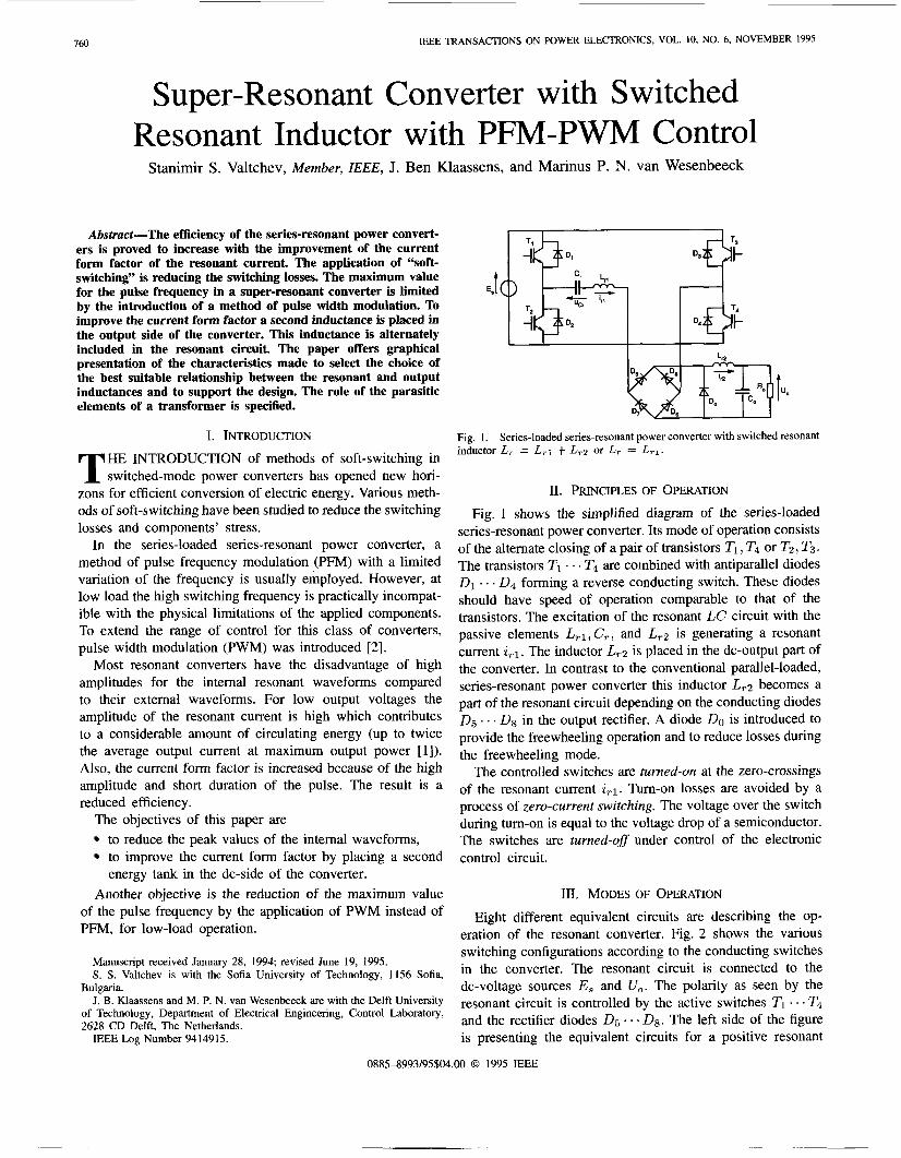
Fig. 1. inductor L, = L,1 + Lrz or L, = L,1.
Series-loaded series-resonant power converter with switched resonant
11. PRINCIPLES OF OPERATION
Fig. 1 shows the simplified diagram of the series-loaded series-resonant power converter. Its mode of operation consists of the alternate closing of a pair of transistors T I , T4 or T2, T3. The transistors Tl . . . T4 are combined with antiparallel diodes D1 . . .D4 forming a reverse conducting switch. These diodes should have speed of operation comparable to that of the transistors. The excitation of the resonant LC circuit with the passive elements L,1, C,, and Lr2 is generating a resonant current Zrl. The inductor Lr2 is placed in the dc-output part of the converter. In contrast to the conventional parallel-loaded, series-resonant power converter this inductor Lr2 becomes a part of the resonant circuit depending on the conducting diodes 0 5 . . .D8 in the output rectifier. A diode DO is introduced to provide the freewheeling operation and to reduce losses during the freewheeling mode.
The controlled switches are turned-on at the zero-crossings of the resonant current iVl. Turn-on losses are avoided by a process of zero-current switching. The voltage over the switch during turn-on is equal to the voltage drop of a semiconductor. The switches are turned-off under control of the electronic control circuit.
111. MODES OF OPERATION
Eight different equivalent circuits are describing the op- eration of the resonant converter. Fig. 2 shows the various switching configurations according to the conducting switches in the converter. The resonant circuit is connected to the dc-voltage sources E, and U,. The polarity as seen by the resonant circuit is controlled by the active switches 7‘1 . . . T4 and the rectifier diodes D5 . . . D8. The left side of the figure is presenting the equivalent circuits for a positive resonant
.OO 0 1995 IEEE

VALTCHEV et al.: SUPER-RESONANT CONVERTER WITH SWITCHED RESONANT INDUCTOR WITH PFM-PWM CONTROL 161
DISC
Fig. 2. Equivalent circuit diagrams.
€4 1 L
current i,l while the right side is presented for a negative resonant current.
The circuits T + and T - present the condition of oper- ation for a power flow from the source to the load. A pair of transistors TI and T4 or T2 and T3 are turned on. The excitation voltage of the resonant circuit is equal to &(Es - U,) . Energy is directly transferred between the source E, and the output U,. The circuits presented as D+ and D- are necessary to reduce the excess of energy stored in the resonant circuit by returning it to the source E, and output U,,. If the inductor ratio Lr1/Lrz is sufficient large, a pair of antiparallel diodes DI and D4, or 0 3 and 0 2 are conducting. The excitation voltage of the resonant circuit is equal to *E,. In case the magnitude of the inductor current i r 2 exceeds the resonant current i r l , the equivalent circuits T F + and T F - represent the operation of the converter. The excitation voltage of the resonant circuit is equal to &E,. For the case that the resonant current irl has become zero but there is still a freewheeling current i r 2 , network F represents the converter network. Finally the diagram DISC at the bottom of Fig. 2 is the equivalent circuit of the converter if no current is flowing (discontinuous conduction mode).
Fig. 3 presents the current is1 through one pair of switches, the resonant current irl and the output current i , ~ , as an illustration of the principles of operation for the continuous conduction mode. The control of the power is performed solely by PFM.
T+ D+ F T- I I
‘k-1 ‘k ‘k+l ‘k+2
Fig. 3. Waveforms for a continuous resonant current i,l (vert: current 5 Ndiv; hor: time 10 ps/div).
Mode D -
At t = t k the diodes D1 and 0 4 starts to conduct because the transistors TZ and T3 are turned off. During mode D- the resonant current is reduced until zero is reached. The equivalent resonant inductor is equal to L,1 while the resonant circuit is excited by a voltage E,. The current i r 2 is decreasing because the voltage over the inductor Lr2 is equal to -U,.
Mode T F +
If the polarity of the resonant current i,l is reversing, the transistor pair TI and T4 goes into conduction avoiding switching losses.

162 IEEE TRANSACTIONS ON POWER ELECTRONICS, VOL. 10, NO. 6, NOVEMBER 1995
+-----------+------...--+...------..+-----------+.------.--~.-~------.-~ Mode T + If the resonant current i,l equals the inductor current i r 2 the
freewheeling diode Do turns-off under zero-voltage conditions. The inductor Lr2 is now included in the resonant network. The equivalent resonant inductor is increased to L, = L,1 + Lr2 which will reduce the di,,/dt ( i = l , 2 ) significantly. By switching the equivalent resonant inductor L, the problem of high peak values for the resonant current is now avoided because the impedance of the resonant circuit is stepwise increased while the resonant frequency is lowered.
Because the resonant current pulse is now similar to a rectangular current pulse, the current form factor becomes close to one which is its optimal value. The dildt at turn- on and turnoff is still limited by the resonant circuits to a
0
+--..-------+--------~--+-----------+-----------+---------~~------~~---~
value that is necessary to obtain a process of soft-switching. T+ F I I I
t k t k + l Mode D+
At t = tk+l the transistor pair TI and T4 is turned off by the control circuit which completes a half cycle of the internal
Fig. 4. 5 Ndiv; hor: time 10 ps/div).
Waveforms for the discontinuous resonant current zri (vert: current
waveforms. Iv. METHODS OF PULSE MODULATION The inductor Lr2 is supposed to have a value for which the
polarity of the voltage over the diode Do becomes positive which drives this diode into conduction. For di, l /dt > di,z/dt the freewheeling diode Do is turned on.
A coefficient K for the ratio of both inductances is intro- duced:
The minimal value for this ratio is calculated as:
where U C , is the amplitude of the voltage over the resonant capacitor C,.
The internal resonant current i,l starts to decrease from the last point where i , l( tk+l) = ir2(tk+1) because the equivalent resonant inductor is reduced to L,1. During this D+ mode the excitation voltage of the resonant circuit is equal to -E,. The current in the inductor Lr2 is now linearly decreasing because the voltage U, over the output capacitor CO is constant.
When the transistor switch is out of saturation and the voltage across the transistor reaches the supply voltage E,, the antiparallel diode starts conducting. The resonant current i , ~ commutates from the switch to an opposite antiparallel diode. Switching from the on- to the off-state is a process without losses. The semiconductor switch stops conducting at full current. The resonant current has initially no other path except than to reduce the stored charge in the transistors until the current starts to decrease after the storage time. In contrast to the series-resonant converter operating at sub- resonant frequencies, the supply voltage is not short-circuited
Super-resonant converters control the average output current by modulation of the amplitude of the resonant current by employing pulse frequency modulation (PFM) [2]. For low output power the amplitude of the resonant current and the amplitude of the voltage uc, max over the resonant capacitor are almost equal to zero. But a resonant capacitor voltage equal to zero causes an infinite switching frequency that is practically incompatible with the physical limitations of the applied active components. Clearly the maximum frequency that can be applied on internal components of a converter is limited for physical reasons.
is lower than the supply voltage E, the resonant current is allowed to be- come discontinuous. This assures that no current is flowing to discharge the resonant capacitor during the interpulse pauses.
The resonant current i,l is zero for mode F or DISC (see Fig. 2) . During the mode F the output current ir2 is fl ywheeling .
The new strategy is to use the switching devices up to their maximum frequency by application of pulse frequency mod- ulation which limits inherently the range of control. Further increase of the range of control is obtained by the introduc- tion of zero-current intervals. In other words: the continuous conduction mode (CCM) is turned into the discontinuous conduction mode (DCM) for which the resonant capacitor voltage UC, stays lower than E,.
Sub-resonant operation is always restricted to use a max- imum resonant capacitor voltage UC, higher than twice the supply voltage E,. The power is mainly regulated by varying the length of the interpulse time (large variation of the switching frequencies for a large range of control).
When the resonant capacitor voltage UC,
U]. The current in an arbitrary switch consists of the diode cur- “lse Width Moduzation
rent (mode D-: negative current in Fig. 3) and the transistor current (mode T F + and T+ in Fig. 3). The diode current segment here is smaller than the transistor current even for a low output voltage (in Fig. 3: U, = 0.3 E,).
To avoid a further increase of the switching frequency to reduce output current, a pulse width modulation process (PWM) is advantageously applied. As presented in Fig. 4 the resonant current is trapezoidal. The same figure shows the

VALTCHEV et al.: SUPER-RESONANT CONVERTER WITH SWITCHED RESONANT INDUCTOR WITH PFM-PWM CONTROL 163
0.2 0'44 0 0 2 4 6 E z,I, E, - 10
Fig. 6. The normalized output voltage q as a function of the normalized output current Z,I,/E, for different values of the current form factor p; for K = 0.
various modes of operation. The output filter capacitor is and can be replaced by a voltage source equal to q = U,/E, . During mode F a flywheeling current i r 2 is running in the flywheel diode Do. If so the equivalent resonant inductor is equal to L,1.
The shape of the resonant current is improved even when the pulses are very short and become triangular as shown in Fig. 5 for discontinuous currents i,l and i r 2 . The output is almost short-circuited ( q = 0.1) resulting in almost equal slopes for the resonant currents (pumping energy into the resonant circuit and returning the energy back to the source).
Fig. 7 shows for the same range of the output voltage q and the output current Z,.I,/E, curves for constant normalized switching frequency F = fsw/f,. where fsw is the switching frequency and f,. is the resonant frequency.
V. DISCUSSION To generalize the presentation a coefficient K is introduced
in (1). The output voltage U, is represented by its normalized value q = U,/E, . All voltages are normalized by dividing with E,, all currents by multiplying with and again dividing by E,.
0 2 4 6 8 10
2 2 - E,
Fig. 7. The normalized output voltage q as a function of the normalized output current Z,I,/E, for different values of the normalized control frequency F = fsw / fT for Ii = 0.
The results of simulation are given in the form of graphical presentations to avoid a complex and cumbersome mathemat- ical analysis. The discussion of the features of the converter is focused on these graphs.
The characteristics of the normalized output voltage q as a function of the normalized output current Z,I,/E, are presented for different values for the current form factors pi . Fig. 6 shows the optimal region of operation for K = 0 (Lr2 = 0 ) as observed for the conventional series-loaded series-resonant power converter. The maximum efficiency should be expected for high output voltages (current form factor pi > 1.11 for q > 0.65) which is not very advantageous if we are looking for a large range of operation.
Fig. 7 shows for the same range of the output voltage q and the output current Z,I,/E, curves for constant normalized switching frequency F = fsw/fr where fsw is the switching frequency and f r is the resonant frequency.
The diagrams for K = 1 (LT2 = L,1) are shown in Figs. 10 and 11. Fig. 10 is different compared to Fig. 6 because the area with a low current form factor is increased. In combination with the control curves of Fig. 11 a wide area of current source operation could be defined with a high efficiency.
The same diagrams are presented for K = 5 (Lr2 = 5Lr1): Figs. 8 and 9. The range of an efficient operation is further increased but at the cost of the voltage-source characteristic at the output terminals.
A large inductor Lr2 shows a tendency to modify the characteristics of a current source at the output terminals. We must take into account that when Lr2 is comparatively high, sharing of currents is difficult if many stages work in parallel. In case of a large Lr2 even a small tolerance in the values of L,2 causes different initial conditions at moment t = t k
for the different stages. It will cause large differences in the intemal resonant currents.
The graphics are useful for the design of the power converter and especially those for L,.2 = L,1 where they were used in practice.

~
764
0.4-
IEEE TRANSACTIONS ON POWER ELECTRONICS, VOL. 10, NO. 6, NOVEMBER 1995
1.10
-12
0.4-\ 1.10
0 2 4 6 8 10 I
GI. - - E S
Fig. 8. The normalized output voltage q as a function of the normalized output current Z,I,/E, for different values of the current form factor p2 for Ii = 1.
0.9
\ \ \ \ 0
Fig. 9. output
0 2 4 6 8 10
- Z,‘, --t E,
The normalized output voltage q as a function of the normalized current Z,I,/E, for different values of the normalized control
frequency F = fswjfr for K = 1.
VI. INFLUENCE OF PARASITIC TRANSFORMER ELEMENTS For this class of converter the average output voltage U,
is lower than the source voltage E, (step-down converter). If necessary a transformer is included in the resonant circuit. Transformers are used for purposes of scaling and insulation.
Technical transformers differ from an ideal transformer because of
1) the existence of inter-winding and inter-turn capacitance, 2) a finite magnetizing inductance. High-voltage transformers have significant inter-turn and
inter-winding capacitances, caused by their physical structure. The equivalent parasitic capacitance C, that is thought to be in parallel with the ac-side of the output rectifier in Fig. 1 is charged as a part of the resonant circuit. The rate of rise of the input voltage of the output rectifier is reduced by this capacitance. Because C, is much smaller than the resonant capacitor C,, the stored energy is small.
In the proposed converter, the stored energy in the capacitive element C, is released, in a non-dissipative manner, by the dis- charging current i r 2 and absorbed by the load. Resonant power
1.06
0.6- 1.08
04 \ \
0 2 4 6 - . 10 L,b
E. --
Fig. 10. The normalized output voltage q as a function of the normalized output current Z,I,/E, for different values of the current form factor pz for I< = 5.
0 2 4 6 8 10 4 ’ 0 * E,
Fig. 1 1 . The normalized output voltage q as a function of the normalized output current Z,I,/E, for different values of the normalized control frequency F = fsw/fr for K = 5.
converters can be designed to include this capacitance as part of their conversion structure thereby efficiently decreasing interactions between the transformer and power converter.
The magnetizing inductance of the transformer L, can be modeled as being in parallel to Cp. Many papers have ad- dressed the problem of the interaction between high-frequency transformers and series-resonant power converters. The so- called transformer induced low frequency oscillations (TLO’s) are generated if a series-resonant converter is operating in the discontinuous conduction mode (DCM) for high conver- sion ratios [3], [4]. TLO’s are causing no problems if the series-resonant power converter is operating in the continuous conduction mode (CCM).
Super-resonant power converters can be operated in CCM without problems over a wide range by pulse frequency modulation. The DCM mode is introduced for very-low output currents. When the super-resonant converter is operating in DCM the amplitude of the resonant capacitor voltage UC, is kept lower than the supply voltage E,. Even now no TLO’s are generated because the driving force for the oscillation (exciting transformer voltage) is avoided.

VALTCHEV et al.: SUPER-RESONANT CONVERTER WITH SWITCHED RESONANT INDUCTOR WITH PFM-PWM CONTROL 165
VII. CONCLUSION
The graphical expressions derived are useful for calculating behavior in the switching modes for a series-resonant circuit. The chosen optimum Lr2 = L,I was used in an experimental 2 kW converter made of several equal output stages where the efficiency was maximized for the highest output power and remains almost constant for lower power levels.
The introduction of a split inductance in a super-resonant converter combined with soft-switching of the semiconductor devices, gives a better current form factor which improves the overall efficiency. At the same time the range of output control can be extended for a limited range of the internal pulse frequency to reduce the devices’ requirements.
The use of PWM control after reaching the maximum switching frequency is not causing difficulties because the resonant capacitor voltage ucr stays lower than the source voltage E,.
It is sufficient to apply control pulses to the transistors with equal length (not so critical to the tolerance of driving and switching devices) and to maintain the tolerance for the passive elements in the usual industrial limits.
The application of a transformer in the series-resonant circuit introduces parasitic components as intenvinding and interturn capacitance and a magnetizing inductance. The par- asitic capacitance C, can be used to smooth the switching process between both inductances at the primary side of the rectifying bridge. The existence of the transformer magnetizing inductance is no longer critical because ucr mm < E,.
As a current source it allows unlimited number of output stages to be connected in parallel without any extra measures to equalize them.
Better efficiency, easy paralleling, and internal short-circuit protection remain advantageous characteristics for any super- resonant converter including this type of power converter.
The converter includes a variety of applications. This con- verter has the optimal features for the class of super-resonant converters (as soft-switching and reduced snubbers). It demon- strates an almost ideal current form factor because of the trapezoidal resonant current shape.
REFERENCES
[ l ] S. S. Valtchev and J. B. Klaassens, “Efficient resonant power conver- sion,” IEEE Trans. Ind. Electron., vol. 37, no. 6, pp. 49W95, Dec. 1990.
[2] S. S. Valtchev, “Some regulation characteristics of PWM series resonant power conversion,” in Proc. 6th Con$ Power Electron. Motion Contr. PEMC, Budapest, Hungary, Oct. 1-3 1990, vol. 1, pp. 83-87.
[3] R. J. King and T. A. Stuart, “Transformer induced instability of the series-resonant converter,” IEEE Trans. Aerosp. Electron. Syst., vol. AES-19, no. 3, pp. 474482, May 1983.
[4] J. B. Klaassens, H. W. Klesser, M. P. N. van Wesenbeeck, and K. van de Wint, “Interaction between a series-resonant converter and a transformer,” in EPE-J., Oct. 1992, pp. 157-164.
[5] R. L. Steigerwald, “High-frequency resonant transistor dc-dc convert- ers,’’ IEEE Trans. Ind. Electron., vol. IE-31, no. 2, pp. 181-191, May 1984.
[6] A. F. Witulski and R. W. Erickson, “Design of the series resonant con- verter for minimum component stress,” IEEE Trans. Aerosp. Electron. Syst., vol. AES-22, no. 4, pp. 356-363, July 1986.
[7] J. Femeux, J. Lavieville, and J. Perard, “Analysis and modeling of dc- dc resonant converter: Application of the resonant switch-mode power supply,” in Proc. PEVSDC’86, pp. 158-163.
[8] R. Steigenvald, “A comparison of half-bridge resonant converter topolo- gies,’’ in Proc. IEEE APEC’87, pp. 135-144.
[9] J. B. Klaassens, “Steady-state analysis of a series-resonant dc-dc con- verter with a bipolar power flow,” IEEE Trans. Ind. Electron., vol. 36, no. 1, pp. 48-55, Feb. 1989.
Stanimir S. Valtchev (M’93) was bom in Lovetch, Bulgaria, on June 13, 1951. He received the M.S. degree in electrical engineering of the Radio- Electronics Faculty of the Higher Institute for Mechanical and Electrical Engineering (VMEI Lenin), named now Technical University Sofia, in 1974.
Until 1977 he worked as a design engineer at the Institute for Medical Equipment, designing analog instrumentation. Since 1977 he has been working at VMEI in the Laboratory of Power Electronics
(excluding the period 1984-1986 when he was with the Laboratory for Manipulators and Robots of the same Institute also as Assistant Director of the Center for Robotics in 1986). Since 1987 he is a Principal Assistant Professor at the Technical University Sofia. He is teaching several courses on Power Supply Equipment and Power Transistor Converters to graduate and post-graduate students. His research interests are in resonant and soft- switching energy conversion employing transistors. During 1987 and in the period 1991-1992 he was with the Laboratory for Power Electronics at the Delft University of Technology in The Netherlands. This stay helped him to initiate the procedure for a Dr.’s Degree submitting in 1993 the preliminary version of a thesis on resonant and soft-switching conversion at super-resonant switching frequencies and passing the exams in 1994 in Sofia. In the period 1990-1994 he was the Deputy Dean for Foreign Students at the TU Sofia. Recently he was invited to Portugal and he is now a consultant for INESC (soft-switching converters) and IST (SABER simulation).
J. Ben Klaassens, for a photograph and biography, see this issue, p. 665.
Marinus P. N. van Wesenbeeck received the B.S. degree in electrical engineering and the M.S. in electrical engineering from the Delft University of Technology in The Netherlands in 1987 and 1989, respectively. He was involved in the research of medium-power soft-switching series-resonant software-controlled power converters as pact of his Ph.D. study.
After graduation he joined the Power Electronics and Electrical Machines Group at Delft University of Technoloev. He recentlv ioined the Drie ”. < . .
Electronics in the Netherlands as a R&D engineer. He is currently involved in the design and development of monophase and polyphase inverters. His professional interests include digital controller systems, inverters, soft-switched power converters and electrical drive systems.
Related Documents