S S u u n n p p l l u u s s C C a a m m e e r r a a S S o o l l u u t t i i o o n n

Welcome message from author
This document is posted to help you gain knowledge. Please leave a comment to let me know what you think about it! Share it to your friends and learn new things together.
Transcript

SSuunnpplluuss CCaammeerraa SSoolluuttiioonn
0z�~H]¶û�ùSPCA500A
Digital Camera Chipset
1999/10/05 Ver. 0.2 Preliminary2
SSPPCCAA550000AA
05 Oct, 1999Ver. 0.2
0z�~H]¶û�ùSPCA500A
Digital Camera Chipset
1999/10/05 Ver. 0.2 Preliminary3
1. General descriptionSPCA500A provides a single chip solution for dual-mode digital camera. It includes image sensor
interface, image processor, storage controller, image compression engine, USB interface and a built-in
micro controller. SPCA500A supports both CCD image sensors and CMOS sensors. The sensor
resolution ranges from VGA to XGA.
2. Feature� Dual mode operation. Support Digital Still Camera mode and PC Camera video mode.
� Still image size 640x480 or 1024x768
� Video image size 640x480, 320x240, 160x120.
� Support both VGA-type and XGA-type CCD sensor :
VGA - SHARP LZ24BP, SONY ICX098AK, PANASONIC MN3777
XGA - SONY ICX204AK, PANASONIC MN3778
� Support VGA CMOS sensor :
HP HDCS-2000, PhotoBit PB320, Hyundai HV7131B, Omnivision QV7610, Pixart PAS002
� Support CDS/AGC/AD :
Hitachi HD49323, Sharp IR3Y38M, EXAR XRDxx, Panasonic AN2104FHQ, ADI AD9803.
� Anti-flicker (60Hz/50Hz) function in Video mode
� Programmable polarity of all Timing control signals for CCD and CDS/AGC/ADC
� Support AE/AWB function.
� Support 16 M SDRAM and 64M (2-bank and 4-bank) SDRAM.
� Store the compressed images in the Flash memory or in the DRAM.
� JPEG-based compression algorithm.
� Programmable Quantization table
� Support 2 M, 4 M & 8M x 8 bit NAND Flash memory for storage image/audio data.
� Hardware generated ECC code for (flash) memory access
� Support a digital interface to access AC-97 device.
� Support USB bus with built-in transceiver.
� Six USB pipes supported, including default Control pipe, Isochronous pipe, Bulk-in pipe, Bulk-out
pipe, Interrupt pipe and Audio pipe.
� Build-in 8032 micro-controller and 4K byte internal data SRAM
� Synchronous Serial Interfaces to control CMOS sensor
� 128pins QFP package.
0z�~H]¶û�ùSPCA500A
Digital Camera Chipset
1999/10/05 Ver. 0.2 Preliminary4
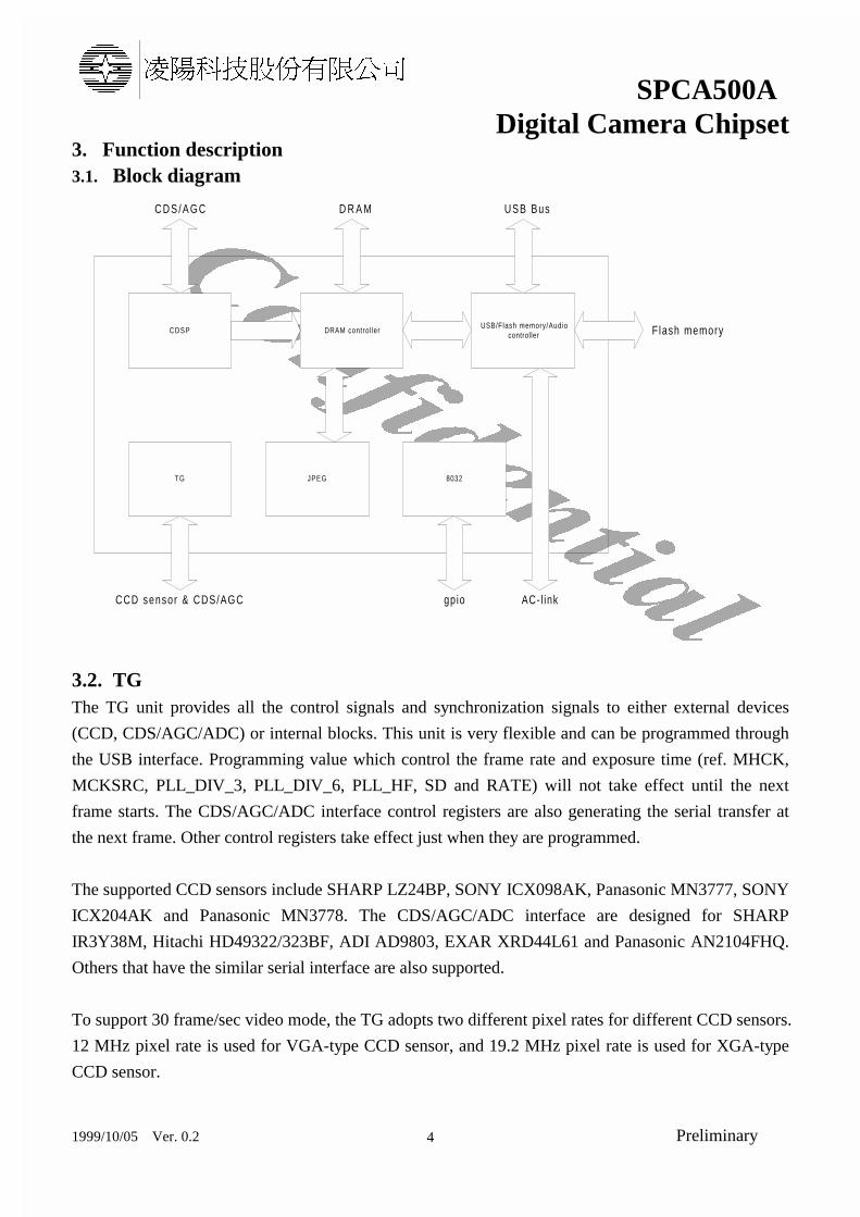
3. Function description3.1. Block diagram
3.2. TGThe TG unit provides all the control signals and synchronization signals to either external devices
(CCD, CDS/AGC/ADC) or internal blocks. This unit is very flexible and can be programmed through
the USB interface. Programming value which control the frame rate and exposure time (ref. MHCK,
MCKSRC, PLL_DIV_3, PLL_DIV_6, PLL_HF, SD and RATE) will not take effect until the next
frame starts. The CDS/AGC/ADC interface control registers are also generating the serial transfer at
the next frame. Other control registers take effect just when they are programmed.
The supported CCD sensors include SHARP LZ24BP, SONY ICX098AK, Panasonic MN3777, SONY
ICX204AK and Panasonic MN3778. The CDS/AGC/ADC interface are designed for SHARP
IR3Y38M, Hitachi HD49322/323BF, ADI AD9803, EXAR XRD44L61 and Panasonic AN2104FHQ.
Others that have the similar serial interface are also supported.
To support 30 frame/sec video mode, the TG adopts two different pixel rates for different CCD sensors.
12 MHz pixel rate is used for VGA-type CCD sensor, and 19.2 MHz pixel rate is used for XGA-type
CCD sensor.
TG
CDSP DRAM control ler
JPEG
USB/Flash memory/Audiocontroller
CCD sensor & CDS/AGC
C D S / A G C D R A M USB Bus
AC-l ink
F lash memory
8032
gp io

0z�~H]¶û�ùSPCA500A
Digital Camera Chipset
1999/10/05 Ver. 0.2 Preliminary5
The serial programming sequence for the CDS/AGC/ADC interface is as follows. First, users set data
to PRG_MODE and CDSBITS as the programming mode, then users write serial data bytes into
CDS_REG1, CDS_REG2 through CDS_REGA. Every writing of CDS_REGA will schedule a serial
data transfer at the next frame start. Bits that exceed the number of CDSBITS will be discarded. Each
data byte is shifted out in MSB-first manner. Several serial interfaces are defined as follows :
PRG_MODE=0 Only SCK, SDATA, no SLOAD signal needed. One dummy SCK pulse cycle to
lead actual data. Every rising SCK to latch SDATA. The falling edge of SCK
which latches SDATA at high denotes the end of transfer. (eg. SHARP IR3Y38M)
PRG_MODE=1 Three signals are used. SCK starts to fall after SLOAD is low. Every rising SCK
to latch SDATA. (eg. Hitachi HD49322BF)
PRG_MODE=2 Three signals are used. SCK starts to rise after SLOAD is low. Every rising SCK
to latch SDATA. (eg. ADI AD9803, EXAR XRD44L61)
PRG_MODE=3 Three signals are used. Every rising SCK to latch SDATA. SLOAD stays low
during SCK is clocking, then one pulse of SLOAD denotes the end of transfer. (eg.
Panasonic AN2104FHQ)

0z�~H]¶û�ùSPCA500A
Digital Camera Chipset
1999/10/05 Ver. 0.2 Preliminary6
� V-Rate timing (still image mode)
0z�~H]¶û�ùSPCA500A
Digital Camera Chipset
1999/10/05 Ver. 0.2 Preliminary7
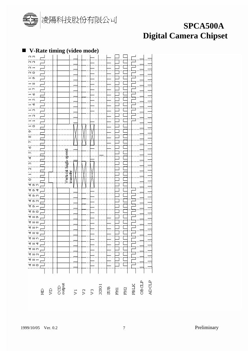
� V-Rate timing (video mode)

0z�~H]¶û�ùSPCA500A
Digital Camera Chipset
1999/10/05 Ver. 0.2 Preliminary8
3.3. CDSPThe CDSP performs optical black compensation, color separation, color correction, edge enhancement,
gamma correction, white balance measurement and exposure measurement. The functional block is
shown.
lin e m emo ryoptical bla ck com pensa tion
color separation
color correction m atrix transform
rgb to yuv
cpu interface w ind ow co ntrolaverage
lum in ance
ccd d ata rgb Y
U V
cpu a ddrcpu d ata
data f low
con tro l flow
There are many parameters could be customized by users. Each parameters is 8-bit which are described
in section 6.2. All of the customized parameter value are updated at the beginning of one frame.
The parameter of the white balance gain denotes the unsigned representation, the integer part 3-bit and
the decimal fraction part 6-bit (ref. Addr 0x8151 to Addr 0x8155).
The parameter of the color correction denotes the 2•s compliment representation, the sign bit, the
integer part 3-bit and the decimal fraction part 4-bit (ref. Addr 0x8108 to Addr 0x8110). The operation
range is from 7.9375 to -8. The color correction performs the following matrix operation :
Rout = A11 * Rin + A12 * Gin + A13 * Bin
Gout = A21 * Rin + A22 * Gin + A23 * Bin
Bout = A31 * Rin + A32 * Gin + A33 * Bin
The parameter of the white balance offset denotes the 2’s compliment representation, the integer part
7-bit and no the decimal fraction part(ref. Addr 0x8111 to Addr 0x8114).
There are six windows for exposure measurement and five windows for white balance measurement.
The window start point (X,Y) is at the most upper left corner. The X is the horizontal axis and equals
to 4 times the parameter value. The Y is the vertical axis and equals to 4 times the parameter value
except window 5. The Y of the window 5 is 2 times the parameter value. The window 1 to the window
4 are the 128x128 pixels. The window 5 and the window 6 are the 256x256 pixels. All of the
window’s position is programmable except the window 6.
0z�~H]¶û�ùSPCA500A
Digital Camera Chipset
1999/10/05 Ver. 0.2 Preliminary9
The average luminance denotes with dynamic range [0~255] (ref. Addr 0x8121 to Addr 0x8126). The
average (R-G)/(B-G) means the average value of (R-G)/(B-G) in the specified window that the
luminance value is greater than the low luminance threshold(Addr 16) and less than the high luminance
threshold(Addr 15). It denotes with dynamic range [-128~+127]. However, the actual average (R-
G)/(B-G) value in the CCDSP module is 2 times the parameter value (ref. Addr 0x8127 to Addr
0x8130).
The spot count value means the total pixel number in the specified window that the luminance value is
greater than the luminance threshold and less than the high luminance threshold . It is a reference value
for auto white balance (ref. Addr 0x8133 and Addr 0x813C).
The look-up table is a programmable function for gamma correction. There are 3 look-up tables for
R,G,B, respectively. Each look-up table have 16 segments. (ref. Addr 0x8190 to Addr 0x81C2)
The USB burst-read can be performed by reading Addr 0x817D, Addr 0x817E and Addr 0x817F
respectively. The burst-read sequence is the window1, window2, window3 and window4. The USB
burst-write can be performed by writing Addr 0x817C. The burst-write sequence is the window1 X,
window1 Y, window2 X, window2 Y, window3 X, window3 Y, window4 X and window4 Y.
The parameter of brightness denotes 2’s complement(Addr 0x8167) and the dynamic range [-128 ~
+127]. The real value of brightness equals 2 times this parameter.
The parameter of contrast(Addr 0x8168) include 1 integer bit and 5 fraction bits. It denotes with
dynamic range [0 ~ 1.96875].
The parameter of saturation(Addr 0x8169) include 1 integer bit and 5 fraction bits. It denotes with
dynamic range [0 ~ 1.96875].
The parameter of hue(Addr 0x816A and 0x816B) include 10 integer bits. It denotes with dynamic
range [0 ~ 719]. Each step represents 0.5 degree.
3.4. JPEGJPEG-based compression algorithm is adopted in the SPCA500A. The Quantization table is
programmable via the JPEG register set. The JPEG compression unit accepts YUV data from the
DRAM controller and outputs the VLC code to the DRAM controller. In the DSC mode, the data is
YUV422 format. In Video mode the data is YUV420 format. MCU (8x8 minimum coding unit)

0z�~H]¶û�ùSPCA500A
Digital Camera Chipset
1999/10/05 Ver. 0.2 Preliminary10
sequence in DSC mode is YYUV and YYYYUV in video mode.
The JPEG compression unit also generates the thumbnail image for the DRAM controller. The
thumbnail image is constructed by the DC-value of each MCU. The size of the thumbnail image in
VGA mode is 80 x 60 and 128 x 96 for the XGA mode.
3.5. DRAM interface
SPCA500A uses DRAM as the frame buffer to hold the incoming image. The DRAM is also used as
temporary compression buffer for the compression unit. Optionally, if the DRAM is chosen to be the
storage element of the camera (instead of flash memory), it can be used to store the compressed image
and thumbnail image. Refer to the DRAM controller register for the different DRAM type and DRAM
size settings. The maximum size supported is 4Mega words. Because the different type of DRAMs
have different number of bits for their column address and row address, it is more convenient for the
DRAM controller to provide a virtual addressing space for the application.
The virtual column address is 10-bit long and row address 12-bit long. This addressing mechanism
yields the maximum space of 4-Mega words. However, if only one 16-Mega bit SDRAM is used in the
application. The addressing space is only 1 Mega word. Normally, if the application uses flash memory
to store the compressed images, there is no need of DRAM with size over 1-Mega words. If the DRAM
is chosen to be the storage, then the application may add more DRAM to increase the number of
images that can be stored in the camera.
The operation of the DRAM controller is different in the DSC mode and in the Video mode :
In the DSC mode : The DRAM controller goes through capture, compress, and saving stage step by
step according to the micro-controller commands. The image size of the DSC mode is fixed at
640x480 for VGA-type CCD sensor, and 1024x768 for XGA-type CCD sensor.
In the Video mode : The DRAM controller operates a bit more automatically. After the input image
accumulates to enough amount for the compression unit, it sends the data to the compression unit in
the format that the compression unit requests. The DRAM controller also accepts data from the
compression unit and stored them in the DRAM temporarily.
In both DSC mode and Video mode, the DRAM controller is responsible to reorder the image data for
appropriate JPEG compression format. Also it must decides the size for image in the variety of the
operation modes.

0z�~H]¶û�ùSPCA500A
Digital Camera Chipset
1999/10/05 Ver. 0.2 Preliminary11
If the DRAM is used as the storage element, the DRAM must enters self-refresh state when the camera
is not in operation. This will save a lot of power. A register bit in the DRAM controller register set is
dedicated to this function. To save image into the DRAM or unload the images from the DRAM, the
micro-controller must set a set of range registers. They define the starting address and ending address
of the saving/unloading area. The data is stored into (or read from) the DRAM in raster-scan order.
Note that the DRAM controller restricts the DRAM range to be set based on a 4-words block. Only
4*N (the multiples of 4) are legal for the starting column address. And only 4N+3 is legal for the
ending column address.
3.6. Embedded Micro ControllerThe SPCA500A has integrated an 8032-compatible micro-controller, a serial communication port and
a build-in 4Kx 8 SRAM. To simplify the firmware development, the users may disable the internal
micro-controller and connect the SPCA500A to an external micro-controller.
PPC CHIP
latch
128K FLASH ROM
addr
[15:
8]
addr
[7:0
]
In ternal CPU connect ion
flashlightigbt_on
gpio1gpio2
pwr1
dido
pclk
pwr2pwr3
(from SPL15A)(to SPL15A)(from SPL15A)
(to SPL15A)
ale
gp io_3
ale
cpuad[7:0]
cpua[15:8]
gpio_0gpio_1gpio_2
gpio_6gpio_5
gpio_7
psenn
a16
cs0nnp
sen
au
gp
io_
5a
ug
pio
_0
r omwrg
pio
_4
augpio_6augpio_7
rxdtxd
p3_0p3_1
int1nn
request
p3_3
augpio_4
For internal 8051 connect ion, the cpu read/wri te s ignals are not routed out of the 128-pin package.
I f using external SRAM, the shadow funct ion for ISP is not supported.
ale
cpuad[7:0]
cpua[15:8]
psen
a16
cs0nn
romwr
augpio_1
p0
p2
data
[7:0
]
External 8051
PPC chip
32K SRAM
la tch
data
[7:0
]
128K FLASH ROM
data
[7:0
]
addr
[7:0
]
Ex terna l CPU connect ion
request
dido
pclk
(from SPL15A)
(to SPL15A) rxdtxd
c s 0 n n
a16
psenn
ale
cpuad[7 :0 ]
cpua[15:8 ]
gp io_5gp io_6gp io_7
(to SPL15A)(from SPL15A)
For external CPU connection, gpio_3 and gpio_2 are used as read/write inputs from the external 8051
rdnn
wrnn
p0
p2
ale
au
gp
io_
0
gp
io_
2g
pio
_3
c s 0 n n
a16
psen
ale
cpuad[7 :0 ]
cpua[15:8 ]
rdnn
wrnn
p0
p2
ale
pse
n
p3
_7
p3
_6
p 3 _ 0p 3 _ 1
p 3 _ 3 int1nn i n t0nn
augp io_4
au
gp
io_
5
addr
[14:
8]
addr
[15:
8]
g p i o_0gp io_1 shadow_on
rom_wr_enn
sha
do
w_
on
pse
nn
wrn
n
wrn
n
rom
_w
r_e
n
WE
B
WE
B
OE
B
0z�~H]¶û�ùSPCA500A
Digital Camera Chipset
1999/10/05 Ver. 0.2 Preliminary12
The micro-controller is similar to DS80C320(Dallas Semiconductor) in terms of hardware features and
instruction cycle timing. However, there are some important differences between the micro-controller
and the DS80C320 :
� Serial ports
The micro-controller does not implement serial port framing error detection and does not implement
slave address comparison for multiprocessor communications.
� Timer 2
The micro-controller does not implement timer2 down-counting mode or the down-count enable
bit(T2MOD, bit0). The timer2 overflow output is active for one clock cycle. In the DS80C320, the
timer2 overflow output is a square wave with a 50% duty cycle.
� Watchdog timer
The micro-controller does not implement an internal watchdog timer.
� Power fail detector
The micro-controller does not implement an internal power fail detector.
� Stop mode
The micro-controller internal cycle counter is reset in stop mode. The micro-controller exits stop
mode only when reset.
� Timed access protection
The micro-controller does not implement timed access protection.
� Serial communication portThe serial communication port is an optional function. It provides a serial communication between
SPCA500A and the external LCD controller(User Interface controller). There are two modes in the
serial communication port. The block diagram is shown below, where UI represents the User
Interface controller and PPC represents SPCA500A :
z Master-slave mode(UI is master, PPC is slave)
UI send one byte command to PPC first, then PPC processor will reply this command with multiple-
byte data(the protocol must be defined first). After the command protocol is finished, another
command can be issued. Otherwise, this command will be queued.
z Slave request mode(PPC request to send command to UI)
PPC make request signal (GPIO) pull high to inform UI that PPC want to send command to UI.
When UI receive this request, UI will finish the unfinished command if any command is still
processing, then UI send out the special command(Grant request) to PPC. Thus, PPC will prepare
the command for UI and pull the request signal to low, then UI will fetch the command and reply it.

0z�~H]¶û�ùSPCA500A
Digital Camera Chipset
1999/10/05 Ver. 0.2 Preliminary13
P C L K
DI
D O
P P C UI
Serial Interface of PPC and UI
(master)(s lave)
P C L K
DI /DO
start bit(2 bits) data bit(8 bi ts) stop bit(1 bit)
Tx device use PCLK r is ing edge to t ransmit data
Rx dev ice use PCLK fa l l ing edge to sample data
PPC and UI are hal f -duplex
NOTE:
R E Q
R E Q
release-bus command
8032 put data on shi f t regand pul l REQ low
DI
3.7. USB
� USB Pipes and Vendor Command
SPCA500A supports the following 6 USB pipes :
Default pipe (EP0) : Process the standard commands and vendor commands.
Video ISO-IN pipe (EP1) : Transmit Video image data (interface 0)
BULK-IN pipe (EP2) : Upload still image to the PC (interface 1)
BULK-OUT pipe (EP3) : Download still image and ROM code - for ISP function (interface 1)
INTERRUPT-IN pipe (EP4) : Transmit device events (interface 1)
Audio ISO-IN pipe (EP5) : Transmit audio data (interface 2)
All standard commands, except the Get Descriptor command, are processed by hardware. For Get
Descriptor command and vendor commands, the USB controller latches the 8-byte commands in the
EP0 FIFO and interrupt the micro-controller. The micro-controller then read the 8-byte command,
decode it, and prepare the appropriate data corresponding the command if necessary. The data, in any,
is then sent to the USB bus by the USB controller.

0z�~H]¶û�ùSPCA500A
Digital Camera Chipset
1999/10/05 Ver. 0.2 Preliminary14
The alternative setting command for each interface is done by hardwire. However, there is a
mechanism to inform firmware if the USB host changes the setting. The mechanism is described as
follows :
1. Record the latest alternative setting.
2. Compare the latest setting (in USB side) with the previous one (in CPU side).
3. If the comparison is different, an interrupt will be asserted to inform the CPU.
4. The CPU writes the value of the alternative setting in USB side to that in CPU side.
� USB Vendor Command for Register Read/Write (for example)
Command bmReqType bRequest wValue wIndex wLength
Read 0C1 0x00 Reserved Address 1
Write 0x41 0x00 High byte :
reserved
low byte: write
value
Address 0
� USB Vendor Command for Image Upload (for example)
Command bmReqType bRequest wValue wIndex wLength
Get thumbnail 0x41 0x01 Image index 0x0000 0x0000
Get image 0x41 0x01 Image index 0x0001 0x0000
Get FAT 0x41 0x01 Reserved 0x0002 0x0000
Get status 0xc1 0x01 Reserved 0x0003 0x0001
� USB Video ISO-IN Packet Format
For the video ISO-IN pipe (the EP1), the host may issue standard commands to change its maximum
packet size. To achieve the optimal system performance, the user must adjust the alternative interface
setting based on the image size and compression rate. The following table shows the maximum packet
sizes for the available alternative interface settings.
Alternative Interface Setting Maximum Packet Size (bytes)
0 0
1 128
2 384
3 512
4 640
5 768
6 896
0z�~H]¶û�ùSPCA500A
Digital Camera Chipset
1999/10/05 Ver. 0.2 Preliminary15
7 1023
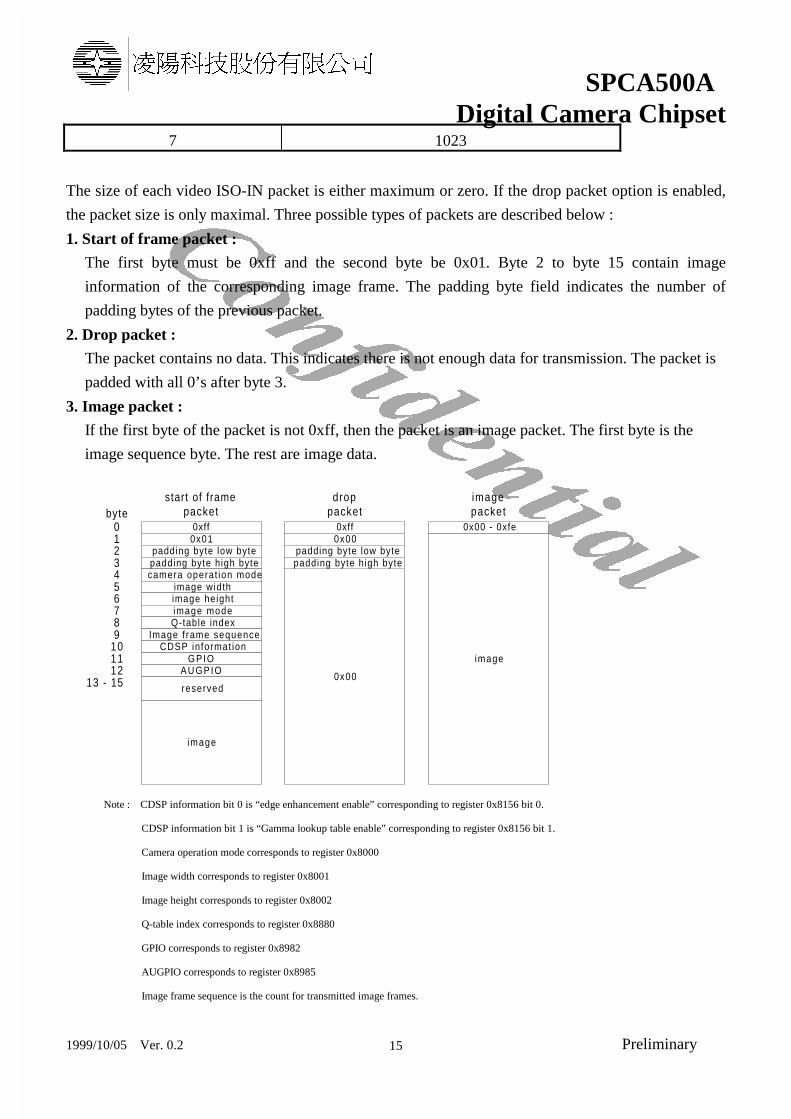
The size of each video ISO-IN packet is either maximum or zero. If the drop packet option is enabled,
the packet size is only maximal. Three possible types of packets are described below :
1. Start of frame packet :
The first byte must be 0xff and the second byte be 0x01. Byte 2 to byte 15 contain image
information of the corresponding image frame. The padding byte field indicates the number of
padding bytes of the previous packet.
2. Drop packet :
The packet contains no data. This indicates there is not enough data for transmission. The packet is
padded with all 0’s after byte 3.
3. Image packet :
If the first byte of the packet is not 0xff, then the packet is an image packet. The first byte is the
image sequence byte. The rest are image data.
Note : CDSP information bit 0 is “edge enhancement enable” corresponding to register 0x8156 bit 0.
CDSP information bit 1 is “Gamma lookup table enable” corresponding to register 0x8156 bit 1.
Camera operation mode corresponds to register 0x8000
Image width corresponds to register 0x8001
Image height corresponds to register 0x8002
Q-table index corresponds to register 0x8880
GPIO corresponds to register 0x8982
AUGPIO corresponds to register 0x8985
Image frame sequence is the count for transmitted image frames.
0xff0x01
padding byte low bytepadding byte high bytecamera operat ion mode
image widthimage heightimage modeQ-table index
Image f rame sequenceCDSP informat ion
GPIOAUGPIO
reserved0x00
byte0123456789
101112
13 - 15
0xff0x00
padding byte low bytepadding byte high byte
image
image
0x00 - 0xfe
start of framepacket
droppacket
imagepacket
0z�~H]¶û�ùSPCA500A
Digital Camera Chipset
1999/10/05 Ver. 0.2 Preliminary16
� USB Bulk-IN Packet Format
The maximum packet size is fixed at 64 bytes. The size of each Bulk-IN packet is either maximum
or zero. Zero-padding is applied to the last packet to make the size maximum if necessary.
� USB Bulk-OUT Packet Format
The maximum packet size is fixed at 64 bytes. The size of each Bulk-OUT packet must be maximal.
� USB Interrupt-IN Packet Format
The maximum packet size is fixed at two bytes. The micro-controller must program the interrupt
pipe registers (both register 0x8506 and 0x8507) after it detects a new event. The USB controller
sends the interrupt data to the host only after register 0x8507 is written.
� USB Audio ISO-IN Packet Format
The maximum packet size may be changed via standard USB commands. The size of each audio
ISO-IN packet is either maximum or zero. The data in the packet is all audio data.
3.8. Flash Memory
The flash memory is used to store still image compression data and thumbnail image. The CPU can
transfer command, address and data to the flash memory by the 8-bit I/O port. There are three
operation modes for the CPU to read/write the flash memory : one is the direct mode, another is the
FIFO mode and the other is pseudo DRAM mode. The ECC that is 22-bit code for every 256 bytes will
be generated in the FIFO mode. The ECC generated by hardware can be read from the registers (3
bytes for 256 bytes/page and 6 bytes for 512 bytes/page). The read/write operation sequence is
described as follows :
1. set the flash memory chip enable
2. set the flash memory command enable (0x8400)
3. write command to the flash memory via the flash memory data register (0x8400)
4. clear the flash memory command enable
5. set the flash memory address enable
6. write address to the flash memory via the flash memory data register (0x8400)
7. clear the flash memory address enable
8. wait the flash memory ready
Direct mode:
0z�~H]¶û�ùSPCA500A
Digital Camera Chipset
1999/10/05 Ver. 0.2 Preliminary17
9. read/write data from/to the flash memory via the flash memory data register(0x8400)
10. read/write additional data from/to the flash memory via the flash memory data register(0x8400)
FIFO mode :
9. read/write data from/to the flash memory via the post buffer data register (0x8300)
10. read the ECC generated by hardware from the ECC registers
11. read/write additional data from/to the flash memory via the flash memory register (0x8400)
Pseudo DMA mode :
9. read the post buffer and write to the flash memory or read the flash memory and write to the post
buffer via the post buffer data register (0x8300)
10. read the ECC generated by hardware from the ECC registers
11. read/write additional data from/to the flash memory via the flash memory register (0x8400)
3.9. Post buffer
� FIFO Control
There are two 1k-byte deep FIFOs in the device to concurrently handle both incoming and outgoing
data stream in various operation modes and to easily handle data for the USB host controller. Some
detailed information about the FIFO is shown as follows :
� Video Camera Mode :
When SPCA500A is operated as a PC camera, the “mode” field in the register (0x8000) must be set to
the video camera mode (0x4). In this mode, the image data will be processed by the front end and then
will be transmitted into the post buffer through DRAM. The data in the post buffer will be read by the
USB host controller through the Bulk-IN pipe or ISO-IN pipe based on the setting at the “VidBulkEn”
field in the register. The deep of post buffer is the same as the maximal packet size of the USB that is
used to transfer the image data in this mode.
� Still Camera Mode :
When SPCA500A is operated as a DSC camera, the “mode” field in the register (0x8000) must be set
to the still camera mode (0x3). In this mode, the image data will be processed and then will be
transmitted into the post buffer through DRAM. The data in the post buffer will be read by the CPU
and written into flash memory by the pseudo DMA mode (1). The deep of post buffer is the same as
the page size of flash memory in this mode.
� Upload Mode (1) :
0z�~H]¶û�ùSPCA500A
Digital Camera Chipset
1999/10/05 Ver. 0.2 Preliminary18
When SPCA500A wants to record sound into flash memory, the “mode” field in the register (0x8000)
must be set to the upload mode (0x1) and the “OprMode” field in the register (0x8301) must be set to
the value of 0x1. In this mode, the CPU will read and process the audio data and then write into flash
memory by the FIFO mode. The deep of post buffer is the same as the page size of flash memory in
this mode.
� Upload Mode (2) :
When SPCA500A wants to read data from flash memory and to transfer through the CPU, for example
RS-232 port, the “mode” field in the register (0x8000) must be set to the upload mode (0x1) and the
“OprMode” field in the register (0x8301) must be set to the value of 0x2. In this mode, the CPU will
read and process data from flash memory by the FIFO mode. The deep of post buffer is the same as the
page size of flash memory in this mode.
� Upload Mode (3) :
When SPCA500A wants to upload data from flash memory to the PC through the USB bus, the
“mode” field in the register (0x8000) must be set to the upload mode (0x1) and the “OprMode” field in
the register (0x8301) must be set to the value of 0x3. In this mode, The data in flash memory will be
read by the CPU and written into post buffer by the pseudo DMA mode (2). The data in the post buffer
will be read through the Bulk-IN pipe by the USB host controller. The deep of post buffer is the same
as the page size of flash memory in this mode.
� Upload Mode (4) :
When the USB host wants to do loop-back test, the “mode” field in the register (0x8000) must be set to
the upload mode (0x1) and the “OprMode” field in the register (0x8301) must be set to the value of
0x4. The forward path is from the PC through Bulk-OUT pipe to the CPU and the backward path is
from the CPU through Bulk-IN pipe to the PC. The backward path is supported in this mode and the
forward path is supported in the next mode, Upload Mode (5). The deep of post buffer is 64 bytes in
this mode.
� Upload Mode (5) :
When the USB host wants to update the ROM code for the CPU on flash memory, the “mode” field in
the register (0x8000) must be set to the upload mode (0x1) and the “OprMode” field in the register
(0x8301) must be set to the value of 0x5. The new ROM code is transmitted into post buffer from the
PC through the Bulk-OUT pipe. Then the CPU reads the post buffer and update the ROM code on the
flash memory. The deep of post buffer is 64 bytes in this mode.
� Upload Mode (6) :

0z�~H]¶û�ùSPCA500A
Digital Camera Chipset
1999/10/05 Ver. 0.2 Preliminary19
When SPCA500A wants to read data from DRAM and to transfer through the CPU, for example RS-
232 port, the “mode” field in the register (0x8000) must be set to the upload mode (0x1) and the
“OprMode” field in the register (0x8301) must be set to the value of 0X6. In this mode, the data is read
from DRAM, transmitted into post buffer and then the CPU will read and process data from post buffer.
In this mode, DRAM is as storage and the deep of post buffer is 64 bytes.
� Upload Mode (7) :
When SPCA500A wants to read data from DRAM and to transfer to the PC through the USB Bulk-IN
pipe, the “mode” field in the register (0x8000) must be set to the upload mode (0x1) and the
“OprMode” field in the register (0x8301) must be set to the value of 0x7. In this mode, the data be
transmitted into the post buffer from DRAM. The data in the post buffer will be read through the Bulk-
IN pipe by the USB host controller. In this mode, DRAM is as storage and the deep of post buffer is 64
bytes.
� Upload Mode (8) :
This is a test mode. In this mode, the “mode” field in the register (0x8000) must be set to the upload
mode (0x1) and the “OprMode” field in the register (0x8301) must be set to the value of 0x8. The CPU
will write, read back and compare data through post buffer and the deep of post buffer is 64 bytes in
this mode.
� Test Mode (0):
This is a test mode. In this mode, the “PBTest” field in the register (0x8304) to the value of 0x01. In
this mode, the data from DRAM will be transmitted into the post buffer. The data in the post buffer
will be forced to read by the CPU and written into flash memory by the pseudo DMA mode (1). The
deep of post buffer is the same as the page size of flash memory in this mode.
� Test Mode (1) :
This is a test mode. In this mode, the “PBTest” field in the register (0x8304) to the value of 0x02. In
this mode, the data from DRAM will be transmitted into the post buffer. The data in the post buffer
will be forced to read through the Bulk-IN pipe by the USB host controller. The deep of post buffer is
64 bytes in this mode.
� Test Mode (2) :
This is a test mode. In this mode, the “PBTest” field in the register (0x8304) to the value of 0x04. In
this mode, the data from DRAM will be transmitted into the post buffer. The data in the post buffer
will be forced to read through the ISO-IN pipe by the USB host controller. The deep of post buffer is
the same as the maximal packet size of the USB that is used to transfer the image data in this mode.
0z�~H]¶û�ùSPCA500A
Digital Camera Chipset
1999/10/05 Ver. 0.2 Preliminary20
3.10. Audio
The audio controller is fully compatible with the AC-97 specification. It provides a digital interface
(AC-link) to access an AC-97 codec. The AC-link is a bi-directional, fixed rate, serial PCM digital
stream. It handles multiple input and output audio streams, as well as control register accesses. The
AC-link architecture divides each audio frame into 12 outgoing and 12 incoming data stream, each
with 20-bit sample resolution.
3.11. Power Control
When SPCA500A is operated in the video camera mode or upload mode, its power is supplied by the
USB bus. According to the USB specification 1.0, no USB device may require more than 100 mA
when first attached, a configured bus-powered USB device attached to a self-powered hub may use up
to 500 mA and all USB devices must support a suspended mode that requires less than 500 uA. When
SPCA500A is operated in the still camera mode, the power is supplied by batteries. So the power
control is quite important. Most major components, such as image sensor module, DRAM, flash
memory and audio device, are power-off when they are not in operation. All the input and bi-
directional signals connected to the chip must be pulled high or low either by internal resistors inside
the chip or by external resistors on the PC board. It prevents these signals from floating. During
suspend state, the clock is stopped and all GPIOs are set to the predefined states (high or low
depending on the register settings). These GPIO’s may be used to control the power switches on the
board. SPCA500A enters suspend state on any one of the following two conditions. First, when
SPCA500A has detected the USB bus is idle for more than 3 ms. Second, a power-down event is
detected on an GPIO pin. Both of the suspend conditions may be enabled or disabled via corresponding
registers (register 0x8013 bit 1:0). Once the suspend event is detected, the micro-controller performs
the suspend procedure and then stop the oscillator of SPCA500A.
SPCA500A exits suspend state when it detects a non-idle state on the USB bus. Another way to wake
up the SPCA500A is activating a predefined wake up pin (a GPIO). The SPCA500A has a built-in
resume counter to ensure it is not in operation until the clock is stable. The built-in micro-controller is
reset automatically after resume is over.
3.12. Synchronous Serial Interfaces
The Synchronous Serial Interfaces is used to program the peripheral IC.
The write sequence :
S Slave Address + wb ACKs Sub Address ACKs Data ACKs P
0z�~H]¶û�ùSPCA500A
Digital Camera Chipset
1999/10/05 Ver. 0.2 Preliminary21
The read sequence :
S Slave Address + wb ACKs Sub Address ACKs
Sr Slave Address + r ACKs Data ACKm P
Or
S Slave Address + wb ACKs Sub Address ACKs P
S Slave Address + r ACKs Data ACKm P
Where S is start condition, ACKs is acknowledge from slave, P is stop, Sr is repeat start condition, and
ACKm is acknowledge from master.
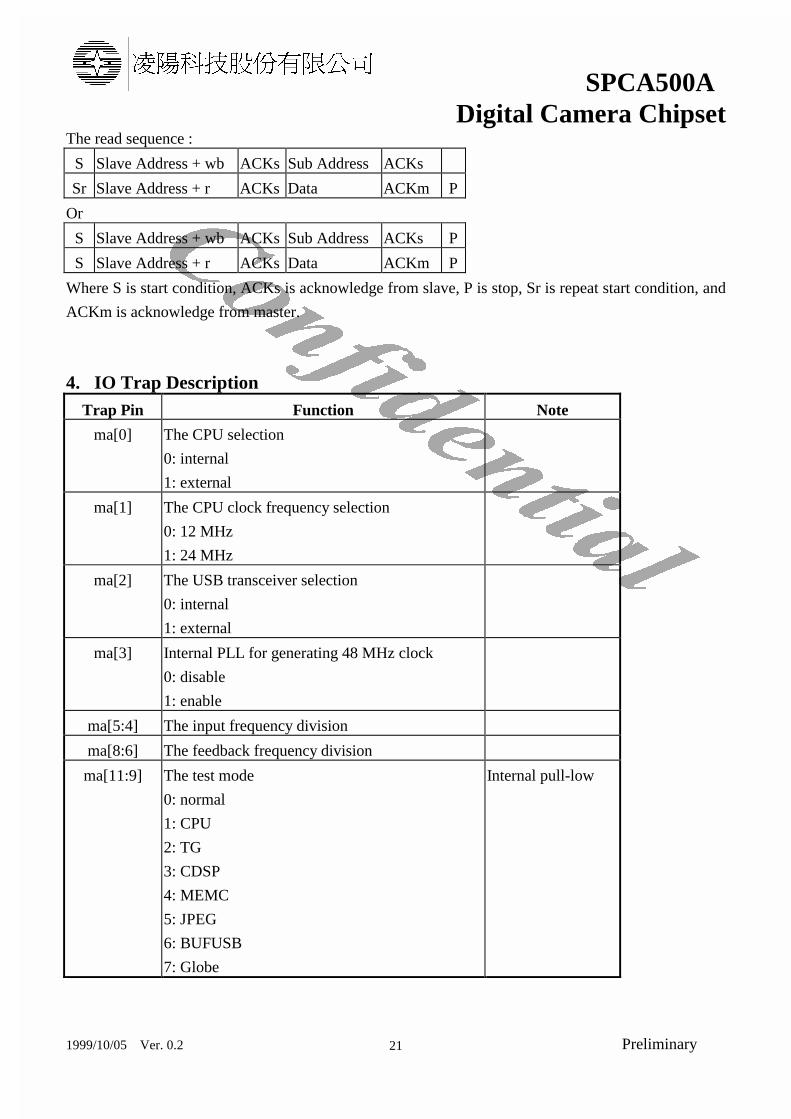
4. IO Trap DescriptionTrap Pin Function Note
ma[0] The CPU selection
0: internal
1: external
ma[1] The CPU clock frequency selection
0: 12 MHz
1: 24 MHz
ma[2] The USB transceiver selection
0: internal
1: external
ma[3] Internal PLL for generating 48 MHz clock
0: disable
1: enable
ma[5:4] The input frequency division
ma[8:6] The feedback frequency division
ma[11:9] The test mode
0: normal
1: CPU
2: TG
3: CDSP
4: MEMC
5: JPEG
6: BUFUSB
7: Globe
Internal pull-low
0z�~H]¶û�ùSPCA500A
Digital Camera Chipset
1999/10/05 Ver. 0.2 Preliminary22
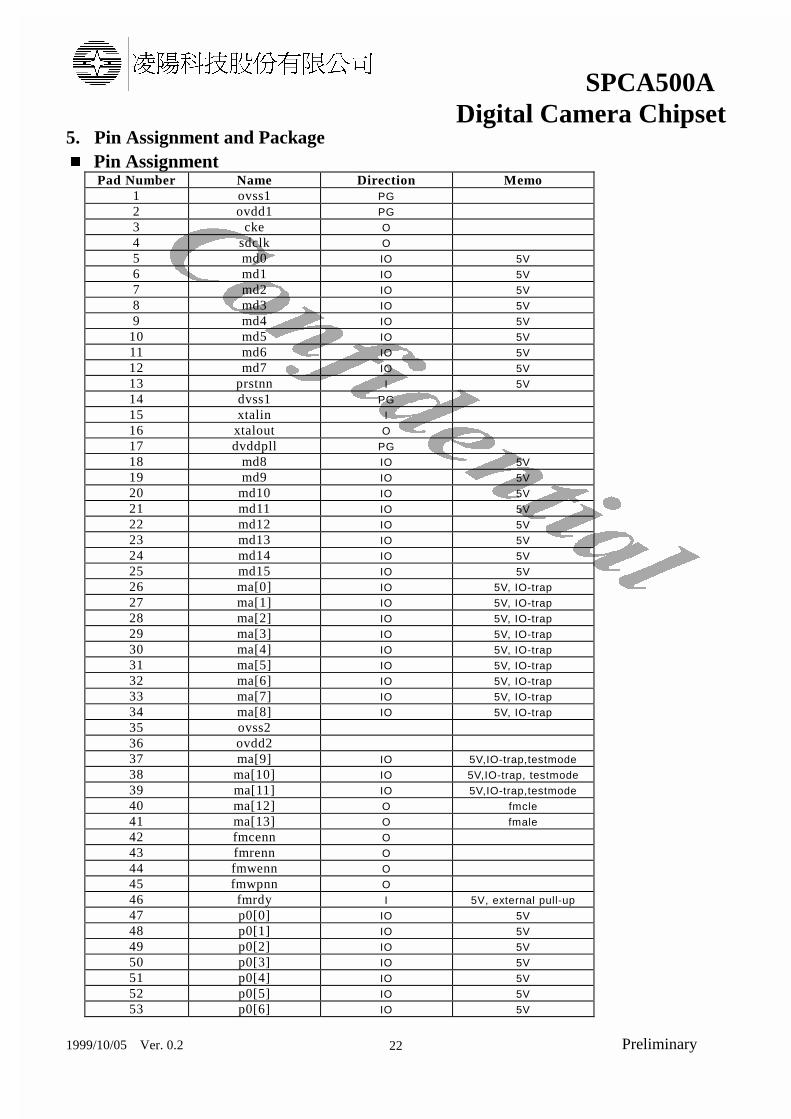
5. Pin Assignment and Package� Pin Assignment
Pad Number Name Direction Memo1 ovss1 PG
2 ovdd1 PG
3 cke O
4 sdclk O
5 md0 IO 5V
6 md1 IO 5V
7 md2 IO 5V
8 md3 IO 5V
9 md4 IO 5V
10 md5 IO 5V
11 md6 IO 5V
12 md7 IO 5V
13 prstnn I 5V
14 dvss1 PG
15 xtalin I
16 xtalout O
17 dvddpll PG
18 md8 IO 5V
19 md9 IO 5V
20 md10 IO 5V
21 md11 IO 5V
22 md12 IO 5V
23 md13 IO 5V
24 md14 IO 5V
25 md15 IO 5V
26 ma[0] IO 5V, IO-trap
27 ma[1] IO 5V, IO-trap
28 ma[2] IO 5V, IO-trap
29 ma[3] IO 5V, IO-trap
30 ma[4] IO 5V, IO-trap
31 ma[5] IO 5V, IO-trap
32 ma[6] IO 5V, IO-trap
33 ma[7] IO 5V, IO-trap
34 ma[8] IO 5V, IO-trap
35 ovss236 ovdd237 ma[9] IO 5V,IO-trap,testmode
38 ma[10] IO 5V,IO-trap, testmode
39 ma[11] IO 5V,IO-trap,testmode
40 ma[12] O fmcle
41 ma[13] O fmale
42 fmcenn O
43 fmrenn O
44 fmwenn O
45 fmwpnn O
46 fmrdy I 5V, external pull-up
47 p0[0] IO 5V
48 p0[1] IO 5V
49 p0[2] IO 5V
50 p0[3] IO 5V
51 p0[4] IO 5V
52 p0[5] IO 5V
53 p0[6] IO 5V

0z�~H]¶û�ùSPCA500A
Digital Camera Chipset
1999/10/05 Ver. 0.2 Preliminary23
54 p0[7] IO 5V
55 dvss256 dvdd257 gpio[0] IO 5V,S
58 gpio[1] IO 5V,S
59 gpio[2] IO 5V,S (ext. cpu write)
60 gpio[3] IO 5V,S(ext. cpu read)
61 gpio[4] IO 5V,S(ROM write)
62 gpio[5] IO 5V,S
63 gpio[6] IO 5V,S
64 gpio[7] IO 5V,S
65 ale IO 5V
66 psenn IO 5V
67 ovss368 ovdd369 p2[0] IO 5V
70 p2[1] IO 5V
71 p2[2] IO 5V
72 p2[3] IO 5V
73 p2[4] IO 5V
74 p2[5] IO 5V
75 p2[6] IO 5V
76 p2[7] IO 5V
77 augpio[0] IO 5V
78 augpio[1] IO 5V
79 augpio[2] IO 5V
80 augpio[3] IO 5V
81 p3[3] IO 5V
82 augpio[4] IO 5V
83 augpio[5] IO 5V
84 augpio[6] IO 5V
85 augpio[7] IO 5V
86 dvss387 dvdd388 ccdrgb[0] I 5V
89 ccdrgb[1] I 5V
90 ccdrgb[2] I 5V
91 ccdrgb[3] I 5V
92 ccdrgb[4] I 5V
93 ccdrgb[5] I 5V
94 ccdrgb[6] I 5V
95 ccdrgb[7] I 5V
96 ccdrgb[8] I 5V
97 ccdrgb[9] I 5V
98 Suspend O
99 Uvdd PG
100 Dm IO
101 Dp IO
102 Uvss PG
103 Vtax IO 5V,S (exthd)
104 Vtbx IO 5V,S (extvd)
105 Vtdx IO
106 Vhax IO
107 Ofd IO
108 Fr IO
109 fh1 IO
110 fh2 IO

0z�~H]¶û�ùSPCA500A
Digital Camera Chipset
1999/10/05 Ver. 0.2 Preliminary24
111 Load IO
112 tvss PG
113 tvdd PG
114 sck IO (Serial clock)
115 sdi IO (Serial data, pull up ext)
116 pblk IO
117 rs IO
118 fs IO CLKX1 output
119 fcds IO CLKX2 output
120 adclp IO 5V,CKx2 input
121 bpx IO
122 adck IO 5V,CKx1 input
123 dvss4 PG
124 dvdd4 PG
125 rasnn O
126 casnn O
127 mwenn O
128 moenndqm O
L: chip internal pull-lowH: chip internal pull-highZ: chip does not drive/pull the pinC: customized on the board (pull-high or pull-low)P: the output enable is programmable via internal register0: chip drive low1: chip drive high5V: 5-volt tolerant IOS: schmitt trigger
0z�~H]¶û�ùSPCA500A
Digital Camera Chipset
1999/10/05 Ver. 0.2 Preliminary25
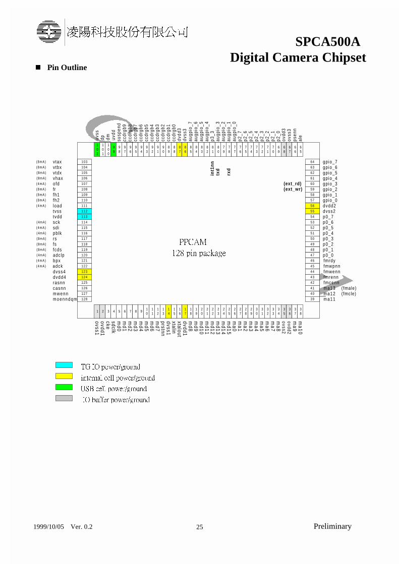
� Pin Outline
ÑÑÄÂÎ
²³¹ ñêï ñâäìâèæ
ÊÐ ãöççæó ñðøæó°èóðöïå
êïõæóïâí äæíí ñðøæó°èóðöïå
ÖÔÃ äæíí ñðøæó°èóðöïå
dvss
3dv
dd3
ovdd
3ov
ss3
augp
io_2
( 4mA)
102
101
100
99
98
97
96
95
94
93
92
91
90
89
88
87
86
85
84
83
1 0 3
1 0 4
1 0 5
1 0 6
1 0 7
1 0 8
1 0 9
1 1 0
1 1 1
1 1 2
1 1 3
1 1 4
1 1 7
1 1 8
1 1 9
1 2 0
1 2 1
1 2 2
1 2 3
1 2 4
1 2 5
1 2 6
1 2 7
1 2 8
6 4
6 3
6 2
6 1
6 0
5 9
5 8
5 7
5 6
5 5
5 4
5 3
5 2
5 1
5 0
4 9
4 8
4 7
4 6
4 5
4 4
4 3
4 0
3 9
4 5 6 7 8 910
11
12
13
16
15
14
17
18
19
20
21
22
23
24
25
26
27
28
29
30
31
32
33
34
35
36
37
38
321
vtaxvtbxvtdxvhaxofdfrfh1fh2load
scksdipblkrsfsfcdsadclpbpxadck
tvdd
(8mA)
(8mA)
(8mA)
(8mA)
(8mA)
(8mA)
(8mA)
(4mA)
(4mA)
(4mA)
(4mA)
(8mA)
(8mA)
(8mA)
(4mA)
(4mA)
(4mA)
augp
io_7
augp
io_6
augp
io_3
p3_3
ckesdclkm
d0m
d1m
d2m
d3m
d4m
d5m
d6m
d7
dvss1
dvdd1
xtalinxtalout
prstnn
md8
md9
md10
md11
md12
md13
md15
ma0
ma1
md14
m a 1 3 (fmale)fmcennfmrennfmwennfmwpnnfmrdy
dvss2
p0_1
p0_3
p0_5
dvdd2
augp
io_0
augp
io_1
t vss
ma2
ÕÈ ÊÐ ñðøæó°èóðöïå
ma3
ma4
ma5
ma6
ma7
ma8
p0_0
p0_2
p0_4
p0_6
ccdr
gb9
ccdr
gb8
ccdr
gb7
ccdr
gb6
ccdr
gb5
ccdr
gb4
ccdr
gb3
ccdr
gb2
ccdr
gb1
ccdr
gb0
d vss4dvdd4rasnncasnnm w e n nm o e n n d q m
ovss1ovdd1
ma9
ma10
ovdd2ovss2
p0_7
gpio_0
gpio_2gpio_1
gpio_3gpio_4gpio_5gpio_6gpio_7
p2_0
p2_1
p2_2
p2_3
p2_6
p2_4
p2_5
p2_7
susp
end
4 2
4 1
1 1 6
1 1 5
82
81
80
79
78
77
76
75
74
73
72
71
70
69
68
67
66
65
aleuv
ss
dm
dp uvdd
psen
n
rxd
txd
int1
nn
(ext_wr)(ext_rd)
m a 1 2m a 1 1
(fmcle)
augp
io_5
augp
io_4
0z�~H]¶û�ùSPCA500A
Digital Camera Chipset
1999/10/05 Ver. 0.2 Preliminary26
� Package dimension
AA2
D
D1
D2
E2E1E
e
b
SUNPLUS
SPCA500A
YYWW ABC
Note : YYWW : Date Code, ABC : Internal Code
Symbol Min. Nom. Max.
A - - 3.4
A2 2.5 2.72 2.9
E 17.20 17.20 17.20
E1 14.00 14.00 14.00
E2 12.50 12.50 12.50
D 23.20 23.20 23.20
D1 20.00 20.00 20.00
D2 18.50 18.50 18.50
e 0.50 0.50 0.50
b 0.17 0.20 0.27
unit : millimeter
Related Documents