MAHARASHTRA STATE BOARD OF TECHNICAL EDUCATION (Autonomous) (ISO/IEC - 27001 - 2013 Certified) SUMMER– 18 EXAMINATION Subject Name: Elements of Electronics Model Answer Subject Code: __________________________________________________________________________________________________ Page No.1/35 17215 Important Instructions to examiners: 1) The answers should be examined by key words and not as word-to-word as given in themodel answer scheme. 2) The model answer and the answer written by candidate may vary but the examiner may tryto assess the understanding level of the candidate. 3) The language errors such as grammatical, spelling errors should not be given moreImportance (Not applicable for subject English and Communication Skills. 4) While assessing figures, examiner may give credit for principal components indicated in thefigure. The figures drawn by candidate and model answer may vary. The examiner may give credit for anyequivalent figure drawn. 5) Credits may be given step wise for numerical problems. In some cases, the assumed constantvalues may vary and there may be some difference in the candidate’s answers and model answer. 6) In case of some questions credit may be given by judgement on part of examiner of relevant answer based on candidate’s understanding. 7) For programming language papers, credit may be given to any other program based on equivalent concept. Q. No. Sub Q. N. Answers Marking Scheme 1 A Attempt any TEN: 20- Total Marks a Write colour code of 1 kΩ resistor. 2M Ans: The colour codeof 1 kΩ resistor is : Brown, Black, Red 2M b Draw the symbol of (i) zener diode, (ii) Schottky diode, (iii) LED, (iv) Tunnel diode. 2M Ans: Zener diode Schottky diode ½ M for each Symbol

Welcome message from author
This document is posted to help you gain knowledge. Please leave a comment to let me know what you think about it! Share it to your friends and learn new things together.
Transcript

MAHARASHTRA STATE BOARD OF TECHNICAL EDUCATION (Autonomous)
(ISO/IEC - 27001 - 2013 Certified)
SUMMER– 18 EXAMINATION Subject Name: Elements of Electronics Model Answer Subject Code:
__________________________________________________________________________________________________
Page No.1/35
17215
Important Instructions to examiners:
1) The answers should be examined by key words and not as word-to-word as given in themodel answer
scheme.
2) The model answer and the answer written by candidate may vary but the examiner may tryto assess the
understanding level of the candidate.
3) The language errors such as grammatical, spelling errors should not be given moreImportance (Not
applicable for subject English and Communication Skills.
4) While assessing figures, examiner may give credit for principal components indicated in thefigure. The
figures drawn by candidate and model answer may vary. The examiner may give credit for anyequivalent
figure drawn.
5) Credits may be given step wise for numerical problems. In some cases, the assumed constantvalues may
vary and there may be some difference in the candidate’s answers and model answer.
6) In case of some questions credit may be given by judgement on part of examiner of relevant answer
based on candidate’s understanding.
7) For programming language papers, credit may be given to any other program based on equivalent
concept.
Q. No.
Sub Q. N.
Answers Marking Scheme
1 A Attempt any TEN: 20- Total Marks
a Write colour code of 1 kΩ resistor. 2M
Ans: The colour codeof 1 kΩ resistor is : Brown, Black, Red 2M
b Draw the symbol of (i) zener diode, (ii) Schottky diode, (iii) LED, (iv) Tunnel diode. 2M
Ans: Zener diode Schottky diode
½ M
for each
Symbol

MAHARASHTRA STATE BOARD OF TECHNICAL EDUCATION (Autonomous)
(ISO/IEC - 27001 - 2013 Certified)
SUMMER– 18 EXAMINATION Subject Name: Elements of Electronics Model Answer Subject Code:
__________________________________________________________________________________________________
Page No.2/35
17215
LED Tunnel diode
c List the two advantages of Bridge Rectifier. 2M
Ans: The advantages of bridge rectifier:
• The output is twice that of the center-tap circuit for the same secondary voltage.
• The PIV is one half that of the center-tap circuit.
• The need for center tapped transformer is eliminated and hence needs a simple
small size transformer.
• Transformer utilization factor, in case of a bridge rectifier, is higher than that of a
centre-tap rectifier.
• There is no possibility of core saturation of transformer secondary winding and
hence transformer losses are reduced.
• It can be used in applications allowing floating output terminals.
Any two 1
mark for
each
d List any four applications of laser diode. 2M
Ans: Applications of LASER diode:
• Fiber optics communication.
• Barcode readers.
• CD players, CD-ROMs and DVD
• Image scanning
• Optical data recording,
• Laser surgery
Any four
½ M
for each
e State different types of filters. 2M
MAHARASHTRA STATE BOARD OF TECHNICAL EDUCATION (Autonomous)
(ISO/IEC - 27001 - 2013 Certified)
SUMMER– 18 EXAMINATION Subject Name: Elements of Electronics Model Answer Subject Code:
__________________________________________________________________________________________________
Page No.3/35
17215
Ans: Types of filters:
1. Series inductor (or choke) filter
2. Shunt capacitor filter
3. Choke input (LC or L type) filter
4. Capacitor input (CLC or πtype) filter
(1/2 mark
for
each type
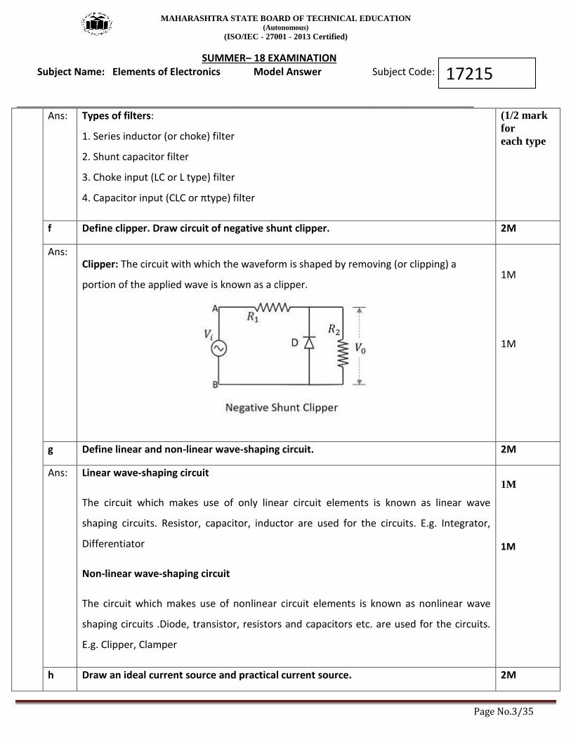
f Define clipper. Draw circuit of negative shunt clipper. 2M
Ans:
Clipper: The circuit with which the waveform is shaped by removing (or clipping) a
portion of the applied wave is known as a clipper.
1M
1M
g Define linear and non-linear wave-shaping circuit. 2M
Ans: Linear wave-shaping circuit
The circuit which makes use of only linear circuit elements is known as linear wave
shaping circuits. Resistor, capacitor, inductor are used for the circuits. E.g. Integrator,
Differentiator
Non-linear wave-shaping circuit
The circuit which makes use of nonlinear circuit elements is known as nonlinear wave
shaping circuits .Diode, transistor, resistors and capacitors etc. are used for the circuits.
E.g. Clipper, Clamper
1M
1M
h Draw an ideal current source and practical current source. 2M
MAHARASHTRA STATE BOARD OF TECHNICAL EDUCATION (Autonomous)
(ISO/IEC - 27001 - 2013 Certified)
SUMMER– 18 EXAMINATION Subject Name: Elements of Electronics Model Answer Subject Code:
__________________________________________________________________________________________________
Page No.4/35
17215
Ans:
Ideal current source Practical current source
Where,
Is = Current Source
Rs = internal resistance of source.
(1 mark
for
each)
i List any two applications of Schottkey diode. 2M
Ans: Application of Schottky diode:
• It is used in rectification of very high frequency signals.
• It is used in communication system circuits.
• It is used in AC to DC converters.
• It is used in Radar system.
• It is used in switched mode power supply.
(Any 2 applications 1 M each)
j Define self-inductance and mutual inductance. 2M
Ans: Self-inductance: As per the Lenz’s law, the self-inducedemf opposes any current change
taking place. This property of the coil to oppose any change in current flowing through it
is known as the self-inductance or inductance.
Mutual inductance: It is defined as the property due to which the change in current
through one coil produces an emf in the other coil placed nearby, by induction. It is
denoted by M and measured in Henry.
(1 mark
for
each)
k State the necessity of wave-shaping circuit. 2M
Ans: Necessity of Wave-shaping circuits:

MAHARASHTRA STATE BOARD OF TECHNICAL EDUCATION (Autonomous)
(ISO/IEC - 27001 - 2013 Certified)
SUMMER– 18 EXAMINATION Subject Name: Elements of Electronics Model Answer Subject Code:
__________________________________________________________________________________________________
Page No.5/35
17215
1. To hold the waveform to a particular d.c level.
2. To generate one waveform from another.
3. To limit the voltage level of the waveform to some preset value and suppress all
other voltage levels in excess of the preset level.
4. To cut off the positive and negative portions of the input waveform.
(OR)
In electronics application, it is often needed to alter the shape of waveform like cutting off
positive or negative portion of wave, generation of one wave from other, holding wave at
some dc level etc. To do this wave shaping circuits are needed.
Correct
statement
2M
l State Kirchoff’ s current law along with its formulae. 2M
Ans: In any electrical network, the algebraic sum of the currents meeting at a point or
junction is zero.
(OR)
Total current entering a junction or node is exactly equal to the total current
leaving the node.
ΣI = 0
m State superposition theorem. 2M

MAHARASHTRA STATE BOARD OF TECHNICAL EDUCATION (Autonomous)
(ISO/IEC - 27001 - 2013 Certified)
SUMMER– 18 EXAMINATION Subject Name: Elements of Electronics Model Answer Subject Code:
__________________________________________________________________________________________________
Page No.6/35
17215
Ans: Superposition theorem:
Superposition theorem states that in any linear network containing two or more sources,
the response (current) in any element is equal to the algebraic sum of the response
(current) caused by individual sources acting alone, while the other sources are replaced
by their internal resistances.
2M
n List any two applications of photo diode and IRLED (each). 2M
Ans: Applications of photo diode:-
• Cameras
• Medical devices
• Safety equipment
• Optical communication device.
Applications of IRLED diode:-
• Light source in optical systems.
• Burglar alarm systems.
• In medical treatment appliances.
• In space optical communication.
(Any 2 applications ½ M each)
(Any 2 applications ½ M each)
Q. No.
Sub Q. N.
Answers Marking Scheme
2 Attempt any FOUR: 16- Total Marks
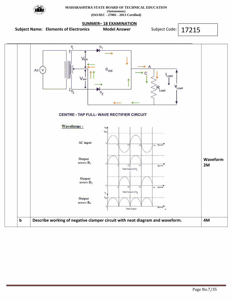
a Draw circuit diagram and waveforms for centre-tap full wave rectifier. 4M
Ans: Circuit Diagram: Circuit diagram 2M
MAHARASHTRA STATE BOARD OF TECHNICAL EDUCATION (Autonomous)
(ISO/IEC - 27001 - 2013 Certified)
SUMMER– 18 EXAMINATION Subject Name: Elements of Electronics Model Answer Subject Code:
__________________________________________________________________________________________________
Page No.7/35
17215
Waveform 2M
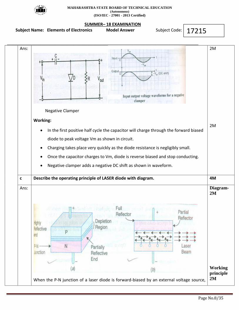
b Describe working of negative clamper circuit with neat diagram and waveform. 4M
MAHARASHTRA STATE BOARD OF TECHNICAL EDUCATION (Autonomous)
(ISO/IEC - 27001 - 2013 Certified)
SUMMER– 18 EXAMINATION Subject Name: Elements of Electronics Model Answer Subject Code:
__________________________________________________________________________________________________
Page No.8/35
17215
Ans:
Negative Clamper
Working:
• In the first positive half cycle the capacitor will charge through the forward biased
diode to peak voltage Vm as shown in circuit.
• Charging takes place very quickly as the diode resistance is negligibly small.
• Once the capacitor charges to Vm, diode is reverse biased and stop conducting.
• Negative clamper adds a negative DC shift as shown in waveform.
2M
2M
c Describe the operating principle of LASER diode with diagram. 4M
Ans:
When the P-N junction of a laser diode is forward-biased by an external voltage source,
Diagram-
2M
Working
principle
2M
MAHARASHTRA STATE BOARD OF TECHNICAL EDUCATION (Autonomous)
(ISO/IEC - 27001 - 2013 Certified)
SUMMER– 18 EXAMINATION Subject Name: Elements of Electronics Model Answer Subject Code:
__________________________________________________________________________________________________
Page No.9/35
17215
electrons move across the junction and recombination occurs in the depletion region
which results in the production of photons. As forward current is increased, more
photons are produced which drift at random in the depletion region. Some of these
photons strike the reflective surface perpendicularly. These reflected photons move back
and forth between the two reflective surfaces. The photon activity becomes so intense
that at some point, a strong beam of laser light comes out of the partially reflective
surface of the diode.
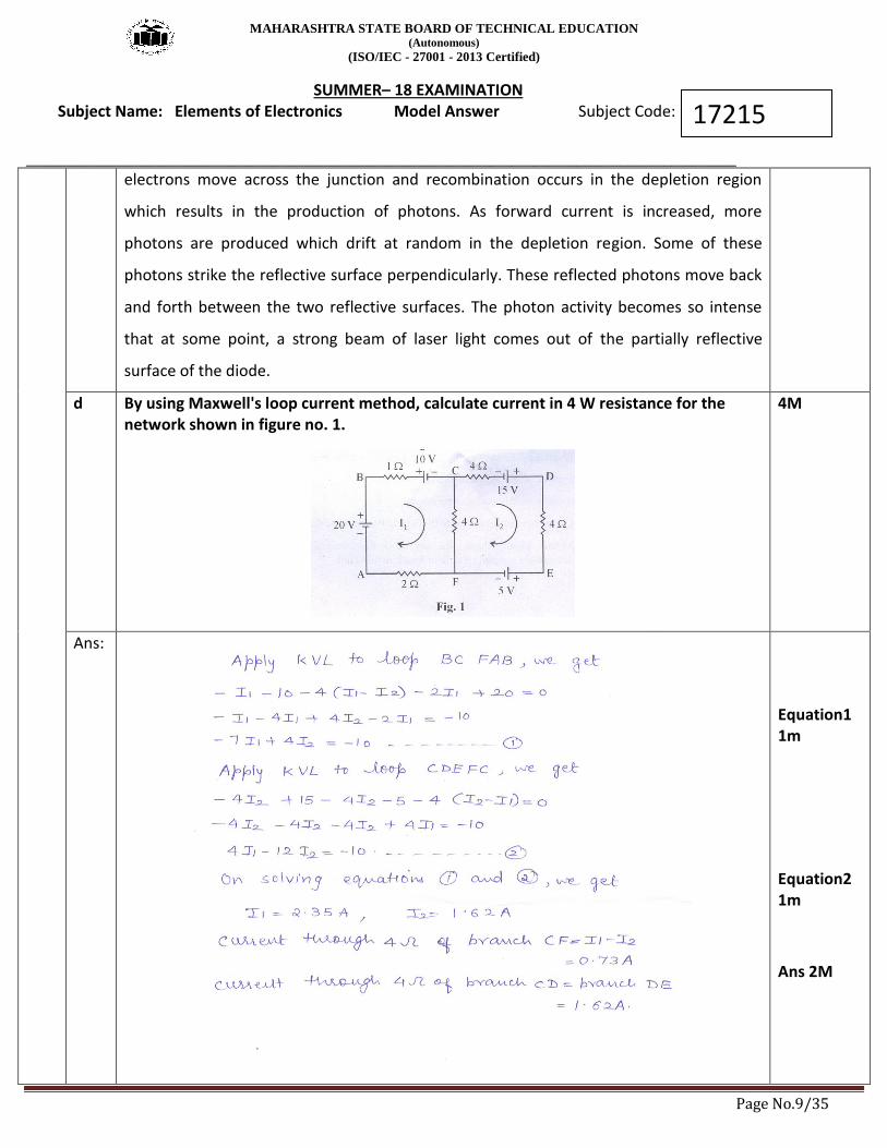
d By using Maxwell's loop current method, calculate current in 4 W resistance for the network shown in figure no. 1.
4M
Ans:
Equation1 1m
Equation2 1m
Ans 2M
MAHARASHTRA STATE BOARD OF TECHNICAL EDUCATION (Autonomous)
(ISO/IEC - 27001 - 2013 Certified)
SUMMER– 18 EXAMINATION Subject Name: Elements of Electronics Model Answer Subject Code:
__________________________________________________________________________________________________
Page No.10/35
17215
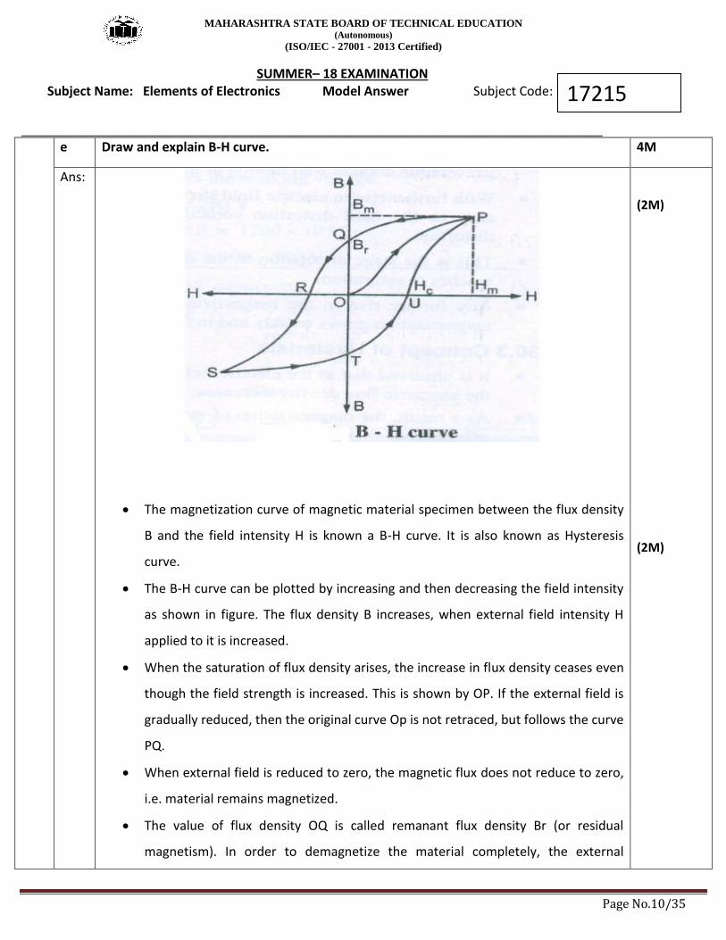
e Draw and explain B-H curve. 4M
Ans:
• The magnetization curve of magnetic material specimen between the flux density
B and the field intensity H is known a B-H curve. It is also known as Hysteresis
curve.
• The B-H curve can be plotted by increasing and then decreasing the field intensity
as shown in figure. The flux density B increases, when external field intensity H
applied to it is increased.
• When the saturation of flux density arises, the increase in flux density ceases even
though the field strength is increased. This is shown by OP. If the external field is
gradually reduced, then the original curve Op is not retraced, but follows the curve
PQ.
• When external field is reduced to zero, the magnetic flux does not reduce to zero,
i.e. material remains magnetized.
• The value of flux density OQ is called remanant flux density Br (or residual
magnetism). In order to demagnetize the material completely, the external
(2M)
(2M)
MAHARASHTRA STATE BOARD OF TECHNICAL EDUCATION (Autonomous)
(ISO/IEC - 27001 - 2013 Certified)
SUMMER– 18 EXAMINATION Subject Name: Elements of Electronics Model Answer Subject Code:
__________________________________________________________________________________________________
Page No.11/35
17215
magnetic field must be reversed and when it reaches the value OR in reverse
direction, it is seen that the flux density is zero.
• Further increase of field intensity in the reverse direction will now increase the
flux density in reverse direction and again at the point S, the saturation occurs.
• The residual magnetism in reverse direction is represented by OT and to neutralize
it the magnetic field intensity must be increased in positive direction to the value
OU. Further increase in field intensity will again magnetize the material and again
saturation will occur at P.
• When the magnetic material is taken through one complete cycle of
magnetization, it traces the loop that is called hysteresis loop. When a material is
subjected to cyclic changes of magnetization, the domains change the direction of
their orientation in accordance with field intensity.
• The work is done in changing the direction of domain which leads to the
production of heat within the material. The energy required to take the material
through one complete cycle of magnetization is proportional to the area enclosed
by the loop.
f Define static and dynamic resistance of diode. 4M
Ans: Static resistance (Rf) :Static Resistance of a P-N junction diode is the ratio of forward
voltage to forward current.
Dynamic Resistance (rf): Dynamic Resistance of a P-N junction diode is the small change
in forward voltage to small change in forward current at a particular operating point.
1M
1M
1M
1M
MAHARASHTRA STATE BOARD OF TECHNICAL EDUCATION (Autonomous)
(ISO/IEC - 27001 - 2013 Certified)
SUMMER– 18 EXAMINATION Subject Name: Elements of Electronics Model Answer Subject Code:
__________________________________________________________________________________________________
Page No.12/35
17215
Q.
No
.
Sub
Q.
N.
Answers Marking
Scheme
3 Attempt any FOUR: 16- Total
Marks
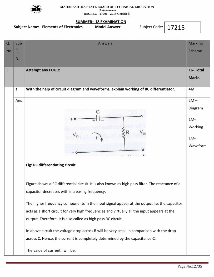
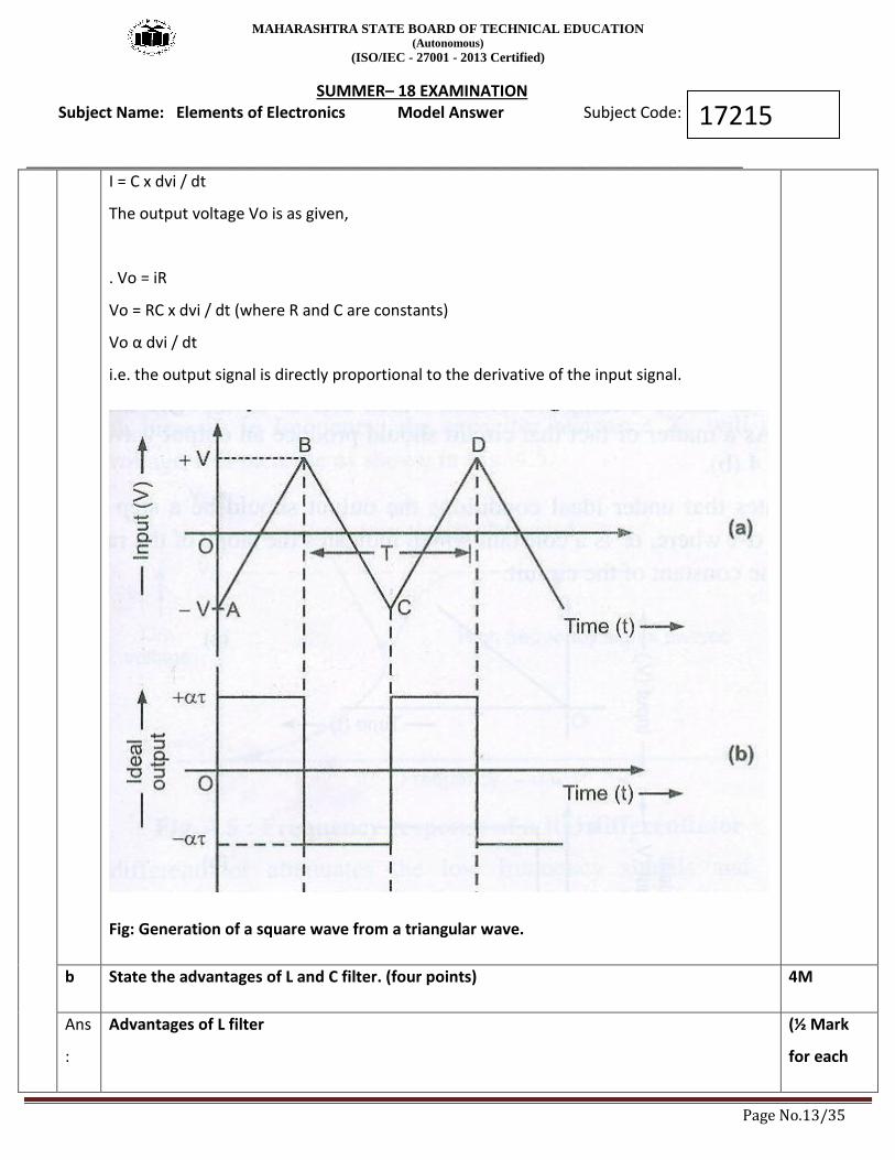
a With the help of circuit diagram and waveforms, explain working of RC differentiator. 4M
Ans
:
Fig: RC differentiating circuit
Figure shows a RC differential circuit. It is also known as high pass filter. The reactance of a
capacitor decreases with increasing frequency.
The higher frequency components in the input signal appear at the output i.e. the capacitor
acts as a short circuit for very high frequencies and virtually all the input appears at the
output. Therefore, it is also called as high pass RC circuit.
In above circuit the voltage drop across R will be very small in comparison with the drop
across C. Hence, the current is completely determined by the capacitance C.
The value of current I will be,
2M –
Diagram
1M-
Working
1M-
Waveform
MAHARASHTRA STATE BOARD OF TECHNICAL EDUCATION (Autonomous)
(ISO/IEC - 27001 - 2013 Certified)
SUMMER– 18 EXAMINATION Subject Name: Elements of Electronics Model Answer Subject Code:
__________________________________________________________________________________________________
Page No.13/35
17215
I = C x dvi / dt
The output voltage Vo is as given,
. Vo = iR
Vo = RC x dvi / dt (where R and C are constants)
Vo α dvi / dt
i.e. the output signal is directly proportional to the derivative of the input signal.
Fig: Generation of a square wave from a triangular wave.
b State the advantages of L and C filter. (four points) 4M
Ans
:
Advantages of L filter
(½ Mark
for each
MAHARASHTRA STATE BOARD OF TECHNICAL EDUCATION (Autonomous)
(ISO/IEC - 27001 - 2013 Certified)
SUMMER– 18 EXAMINATION Subject Name: Elements of Electronics Model Answer Subject Code:
__________________________________________________________________________________________________
Page No.14/35
17215
1. It has low ripple factor at heavy load currents (i.e. low load resistance)
2. It has no surge current through the diode.
3. It reduces the ripple in the DC output of rectifier circuit.
4. The L filter is more suitable for heavy loads.
Advantages of C filter
1. It is easy to design
2. It is small in size and cheap
3. It has low ripple factor for heavy loads.
4. It has high output DC voltage for light loads.
5. It is more suitable for light loads.
6. It has no load voltage equal to maximum transformer voltage.
correct
point)
(½ Mark
for each
correct
point)
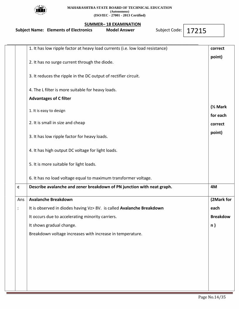
c Describe avalanche and zener breakdown of PN junction with neat graph. 4M
Ans
:
Avalanche Breakdown
It is observed in diodes having Vz> 8V. is called Avalanche Breakdown
It occurs due to accelerating minority carriers.
It shows gradual change.
Breakdown voltage increases with increase in temperature.
(2Mark for
each
Breakdow
n )
MAHARASHTRA STATE BOARD OF TECHNICAL EDUCATION (Autonomous)
(ISO/IEC - 27001 - 2013 Certified)
SUMMER– 18 EXAMINATION Subject Name: Elements of Electronics Model Answer Subject Code:
__________________________________________________________________________________________________
Page No.15/35
17215
Zener Breakdown
It is observed in diodes having Vz = 5 – 8V. is called Zener Breakdown.
It occurs due to increased electric field.
Breakdown is very sharp.
Breakdown voltage decreases with increase in temperature
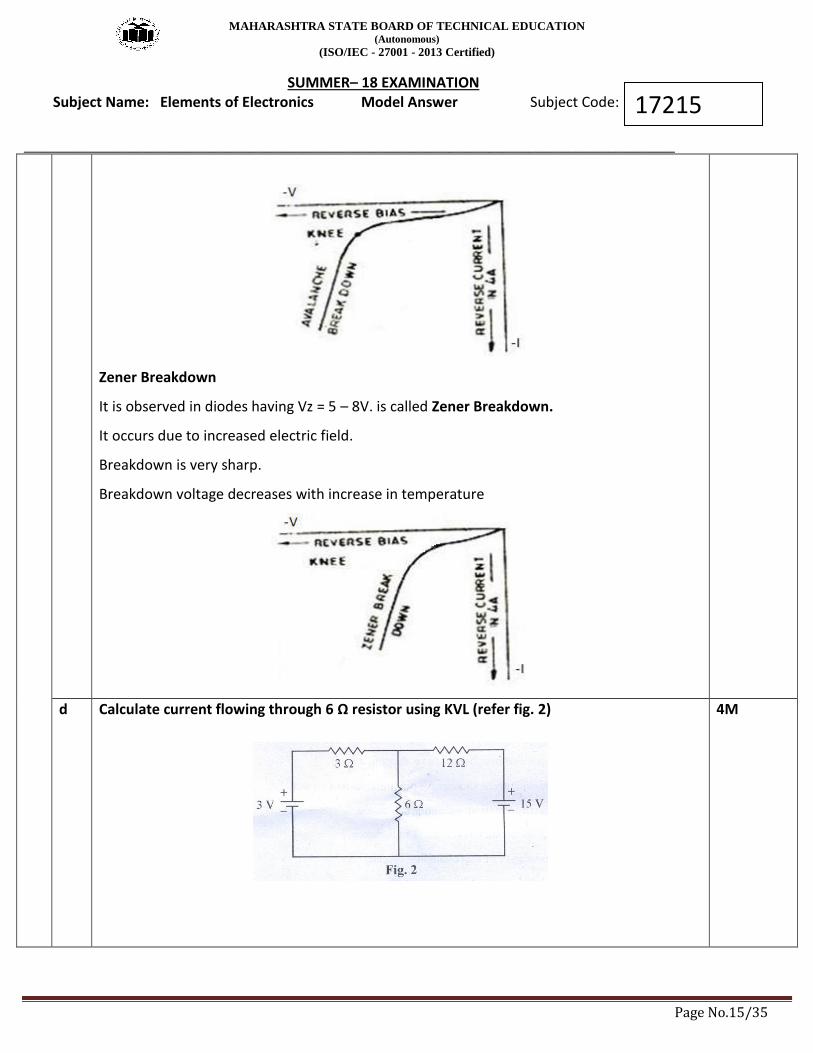
d Calculate current flowing through 6 Ω resistor using KVL (refer fig. 2)
4M
MAHARASHTRA STATE BOARD OF TECHNICAL EDUCATION (Autonomous)
(ISO/IEC - 27001 - 2013 Certified)
SUMMER– 18 EXAMINATION Subject Name: Elements of Electronics Model Answer Subject Code:
__________________________________________________________________________________________________
Page No.16/35
17215
Ans
:
Note: (Marks may be awarded to solution by any other method)
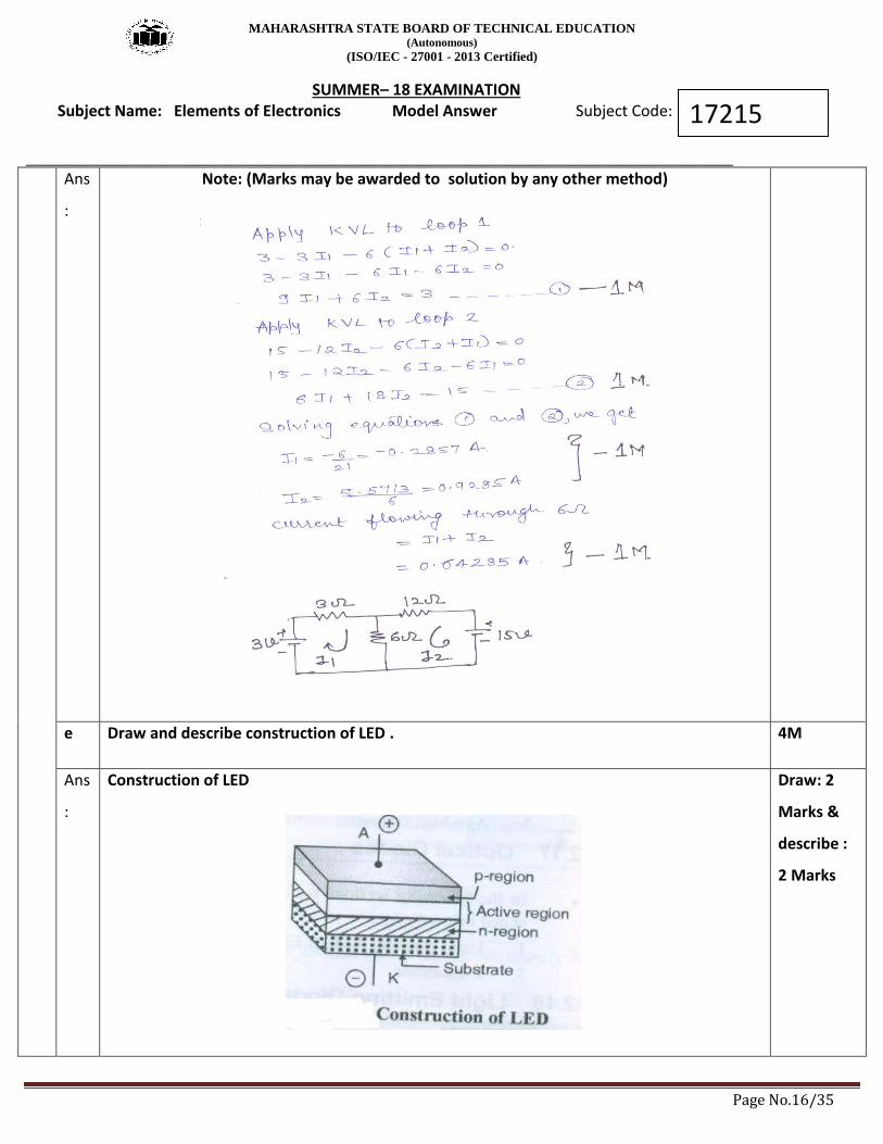
e Draw and describe construction of LED . 4M
Ans
:
Construction of LED
Draw: 2
Marks &
describe :
2 Marks
MAHARASHTRA STATE BOARD OF TECHNICAL EDUCATION (Autonomous)
(ISO/IEC - 27001 - 2013 Certified)
SUMMER– 18 EXAMINATION Subject Name: Elements of Electronics Model Answer Subject Code:
__________________________________________________________________________________________________
Page No.17/35
17215
Fig above shows the construction of LED.
Here an N-type layer is grown on a substrate by a diffusion process.
Then a thin P-type layer is grown on the N-type layer.
The metal connections to both the layers make anode and cathode terminals as indicated.
The active region exists between the P and N regions.
The light energy is released at the junction when the electron hole pair recombination takes
place.
After passing through the P-region the light is emitted from the window provided at top.
f Define given parameters and state their values for bridge rectifier (i) Ripple factor (ii) PIV
of diode.
4M
Ans
:
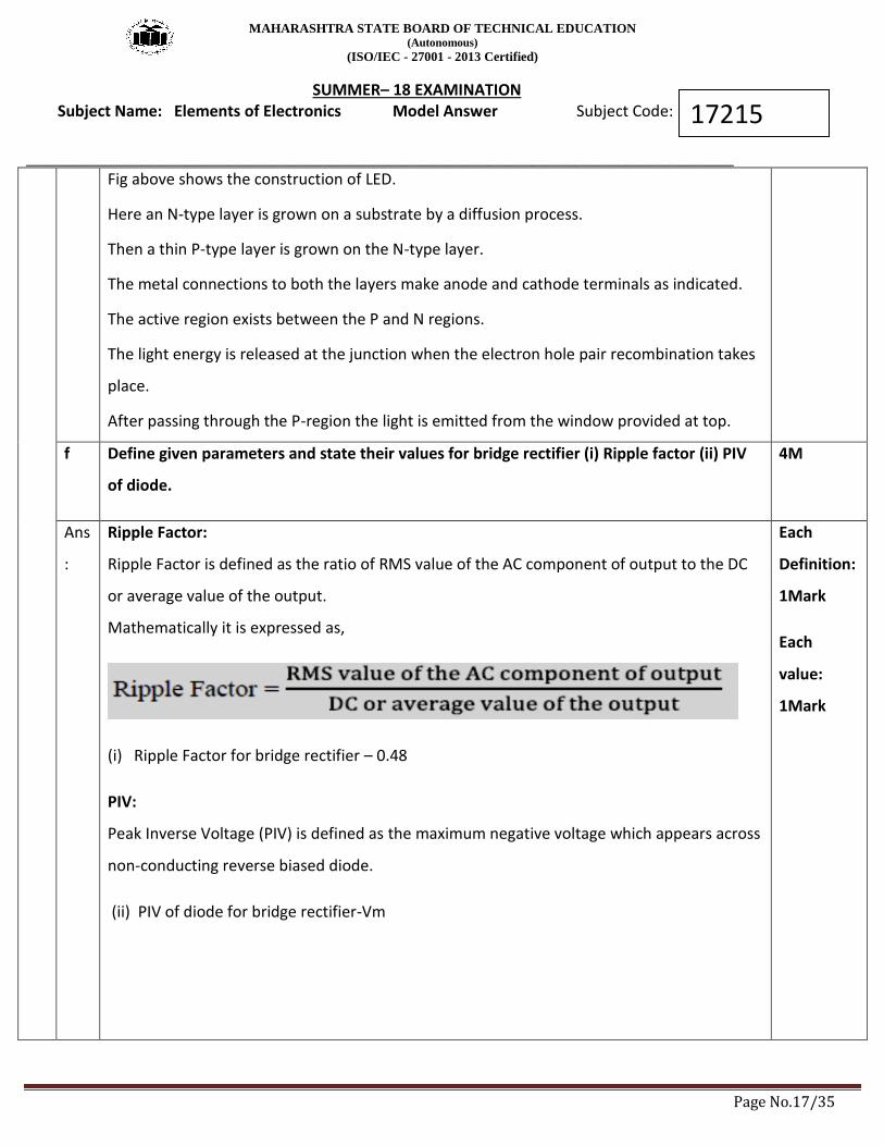
Ripple Factor:
Ripple Factor is defined as the ratio of RMS value of the AC component of output to the DC
or average value of the output.
Mathematically it is expressed as,
(i) Ripple Factor for bridge rectifier – 0.48
PIV:
Peak Inverse Voltage (PIV) is defined as the maximum negative voltage which appears across
non-conducting reverse biased diode.
(ii) PIV of diode for bridge rectifier-Vm
Each
Definition:
1Mark
Each
value:
1Mark
MAHARASHTRA STATE BOARD OF TECHNICAL EDUCATION (Autonomous)
(ISO/IEC - 27001 - 2013 Certified)
SUMMER– 18 EXAMINATION Subject Name: Elements of Electronics Model Answer Subject Code:
__________________________________________________________________________________________________
Page No.18/35
17215
Q.
No
.
Sub
Q.
N.
Answers Marking
Scheme
4 Attempt any FOUR: 16- Total
Marks
a Write down the colour code for the following resistors :
(i) 150 Ω ± 5% (ii) 3.3kΩ ± 20%
4M
Ans
:
i. 150 Ω ± 5%
15 x 101 ± 5%
Brown,Green,Brown,Gold
ii. 3.3kΩ ± 20%
3 3 x 10² ± 20%
Orange, Orange, Red, no colour
Correct
Code – 2
Marks Each
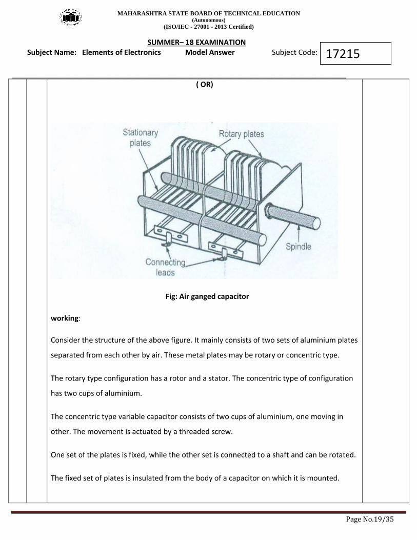
b Describe working of variable air gang capacitor with neat sketch. 4M
Ans
:
2M-
Diagram
2M-
Working
MAHARASHTRA STATE BOARD OF TECHNICAL EDUCATION (Autonomous)
(ISO/IEC - 27001 - 2013 Certified)
SUMMER– 18 EXAMINATION Subject Name: Elements of Electronics Model Answer Subject Code:
__________________________________________________________________________________________________
Page No.19/35
17215
( OR)
Fig: Air ganged capacitor
working:
Consider the structure of the above figure. It mainly consists of two sets of aluminium plates
separated from each other by air. These metal plates may be rotary or concentric type.
The rotary type configuration has a rotor and a stator. The concentric type of configuration
has two cups of aluminium.
The concentric type variable capacitor consists of two cups of aluminium, one moving in
other. The movement is actuated by a threaded screw.
One set of the plates is fixed, while the other set is connected to a shaft and can be rotated.
The fixed set of plates is insulated from the body of a capacitor on which it is mounted.

MAHARASHTRA STATE BOARD OF TECHNICAL EDUCATION (Autonomous)
(ISO/IEC - 27001 - 2013 Certified)
SUMMER– 18 EXAMINATION Subject Name: Elements of Electronics Model Answer Subject Code:
__________________________________________________________________________________________________
Page No.20/35
17215
The set of moving aluminium plates can be moved in or out of a fixed set of plates with the
help of a suitable knob connected to a rotating shaft. As the plates are moved in and out of
the fixed plates, the capacitance value varies.
The capacitance is minimum, when the moving plates are completely out and it is
maximum, when the moving plates are completely in.
The fixed plates are called stators, which are normally made of brass, copper or aluminium.
The cadmium plated steel is used for the frames in low cost capacitors.
The outer set of plates is called rotors. They get interleaved with stators, when the shaft is
rotated. Sometimes, two or more such capacitors are operated by a single shaft.
c Describe the working of PN junction diode with neat sketch under forward biased
condition.
4M
Ans
:
Working of PN junction diode under forward biased condition with help of following circuit
diagram and graph
Region A to B:
In this region A to B of the forward characteristics shown in the fig, the forward voltage is
small and less than the cut in voltage.
Therefore the forward current flowing through the diode is small.
With further increase in the forward voltage, it reaches the level of the cut in voltage and
the width of depletion region grows on decreasing.
Region B to C:
As soon as the forward voltage equals the cut in voltage, current through the diode
increases suddenly. The nature of this current is exponential.
The large forward current in the region B-C of the forward characteristics is limited by
connecting a resistor ‘R’ in series with the diode. Forward current is of the order of a few
mA.
The forward current is a conventional current that flows from anode to cathode.
Working:2
M
Graph:2M
MAHARASHTRA STATE BOARD OF TECHNICAL EDUCATION (Autonomous)
(ISO/IEC - 27001 - 2013 Certified)
SUMMER– 18 EXAMINATION Subject Name: Elements of Electronics Model Answer Subject Code:
__________________________________________________________________________________________________
Page No.21/35
17215
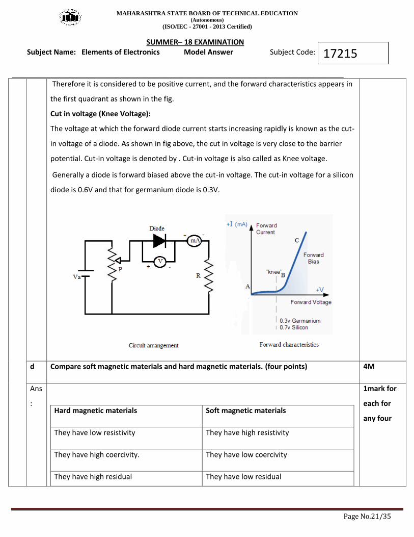
Therefore it is considered to be positive current, and the forward characteristics appears in
the first quadrant as shown in the fig.
Cut in voltage (Knee Voltage):
The voltage at which the forward diode current starts increasing rapidly is known as the cut-
in voltage of a diode. As shown in fig above, the cut in voltage is very close to the barrier
potential. Cut-in voltage is denoted by . Cut-in voltage is also called as Knee voltage.
Generally a diode is forward biased above the cut-in voltage. The cut-in voltage for a silicon
diode is 0.6V and that for germanium diode is 0.3V.
d Compare soft magnetic materials and hard magnetic materials. (four points) 4M
Ans
:
Hard magnetic materials Soft magnetic materials
They have low resistivity They have high resistivity
They have high coercivity. They have low coercivity
They have high residual They have low residual
1mark for
each for
any four
MAHARASHTRA STATE BOARD OF TECHNICAL EDUCATION (Autonomous)
(ISO/IEC - 27001 - 2013 Certified)
SUMMER– 18 EXAMINATION Subject Name: Elements of Electronics Model Answer Subject Code:
__________________________________________________________________________________________________
Page No.22/35
17215
magnetism magnetism.
They have high (B*H) energy They have low (B*H) energy
They have high retentivity. They have low retentivity
They cannot be easily magnetized They are easily magnetized.
They have wide hysteresis loop. They have narrow hysteresis loop.
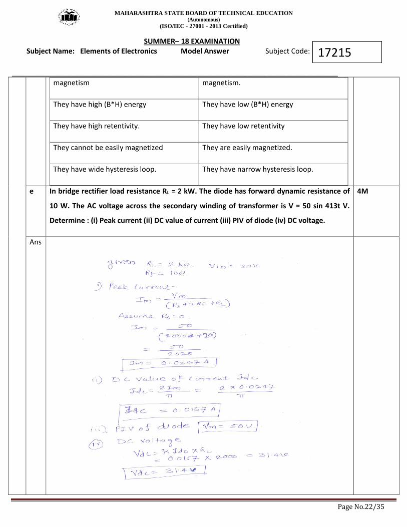
e In bridge rectifier load resistance RL = 2 kW. The diode has forward dynamic resistance of
10 W. The AC voltage across the secondary winding of transformer is V = 50 sin 413t V.
Determine : (i) Peak current (ii) DC value of current (iii) PIV of diode (iv) DC voltage.
4M
Ans
MAHARASHTRA STATE BOARD OF TECHNICAL EDUCATION (Autonomous)
(ISO/IEC - 27001 - 2013 Certified)
SUMMER– 18 EXAMINATION Subject Name: Elements of Electronics Model Answer Subject Code:
__________________________________________________________________________________________________
Page No.23/35
17215
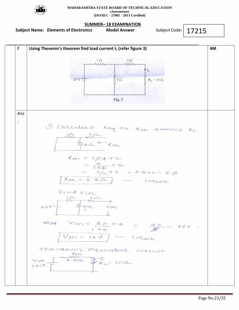
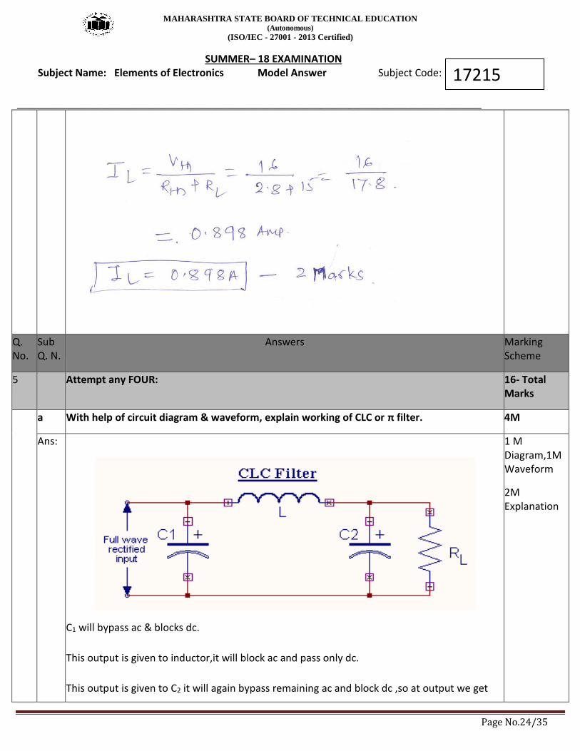
f Using Thevenin's theorem find load current IL (refer figure 3)
4M
Ans
:
MAHARASHTRA STATE BOARD OF TECHNICAL EDUCATION (Autonomous)
(ISO/IEC - 27001 - 2013 Certified)
SUMMER– 18 EXAMINATION Subject Name: Elements of Electronics Model Answer Subject Code:
__________________________________________________________________________________________________
Page No.24/35
17215
Q. No.
Sub Q. N.
Answers Marking Scheme
5 Attempt any FOUR: 16- Total Marks
a With help of circuit diagram & waveform, explain working of CLC or π filter. 4M
Ans:
C1 will bypass ac & blocks dc.
This output is given to inductor,it will block ac and pass only dc.
This output is given to C2 it will again bypass remaining ac and block dc ,so at output we get
1 M Diagram,1M Waveform
2M Explanation
MAHARASHTRA STATE BOARD OF TECHNICAL EDUCATION (Autonomous)
(ISO/IEC - 27001 - 2013 Certified)
SUMMER– 18 EXAMINATION Subject Name: Elements of Electronics Model Answer Subject Code:
__________________________________________________________________________________________________
Page No.25/35
17215
ripple free dc.
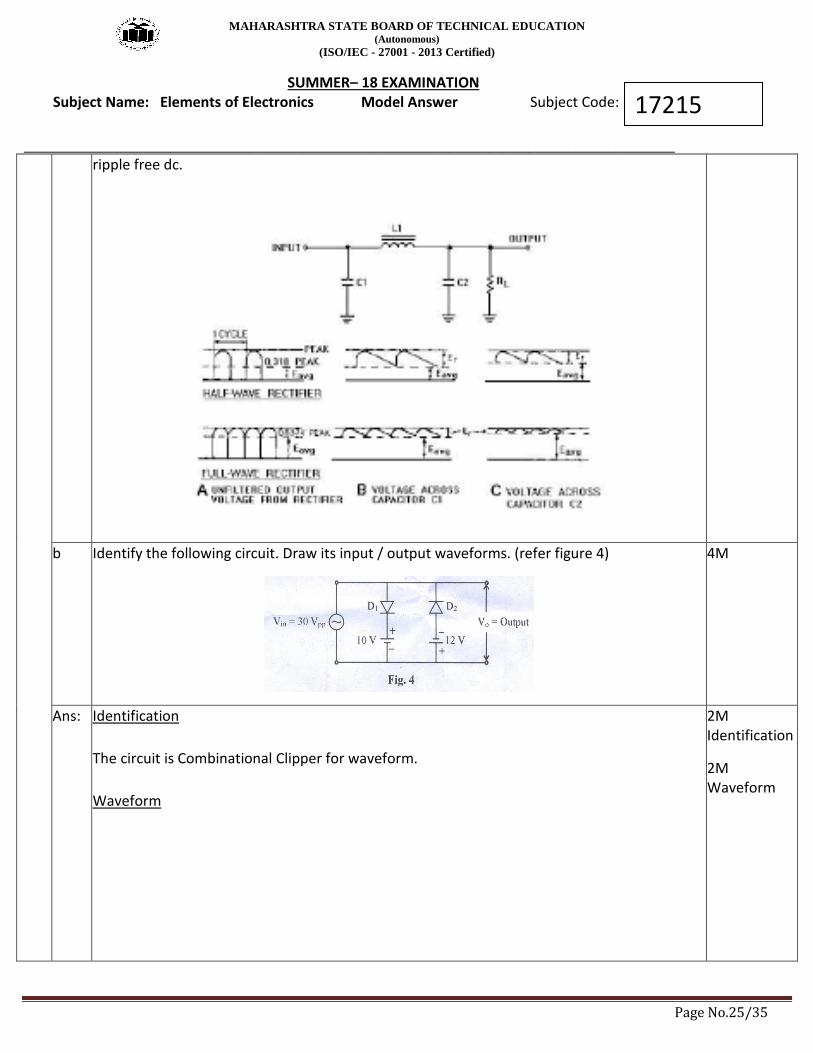
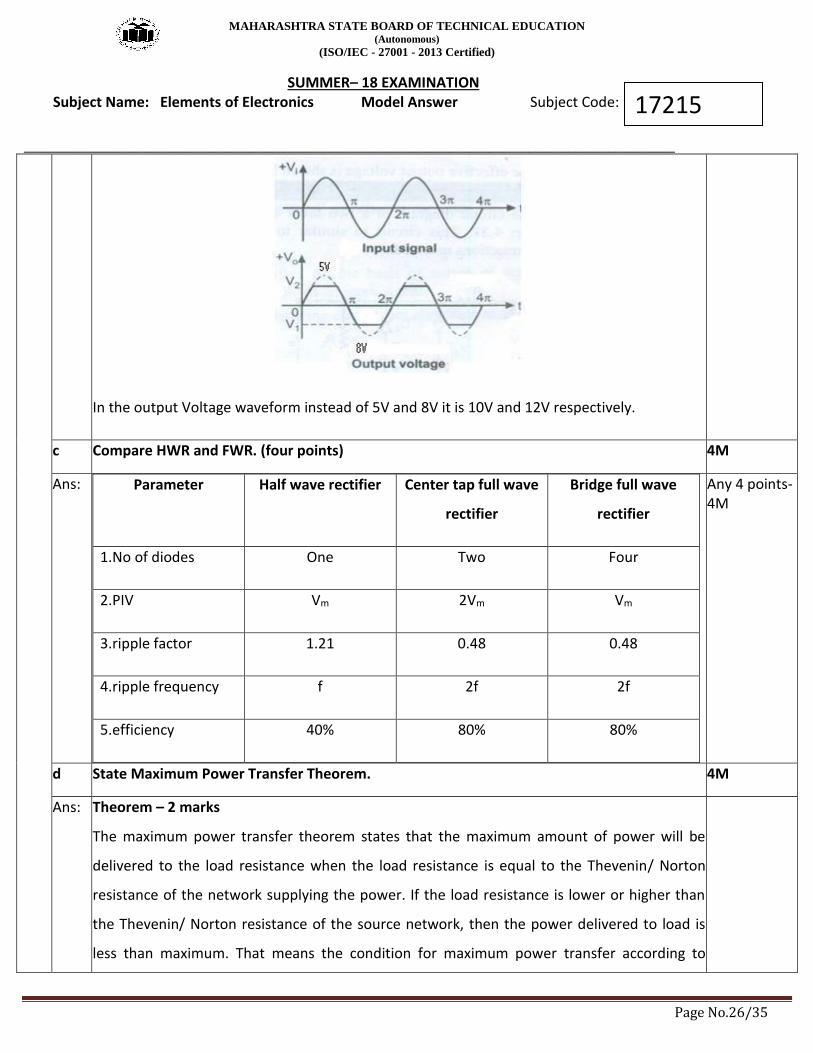
b Identify the following circuit. Draw its input / output waveforms. (refer figure 4)
4M
Ans: Identification
The circuit is Combinational Clipper for waveform.
Waveform
2M Identification
2M Waveform
MAHARASHTRA STATE BOARD OF TECHNICAL EDUCATION (Autonomous)
(ISO/IEC - 27001 - 2013 Certified)
SUMMER– 18 EXAMINATION Subject Name: Elements of Electronics Model Answer Subject Code:
__________________________________________________________________________________________________
Page No.26/35
17215
In the output Voltage waveform instead of 5V and 8V it is 10V and 12V respectively.
c Compare HWR and FWR. (four points) 4M
Ans: Parameter Half wave rectifier Center tap full wave
rectifier
Bridge full wave
rectifier
1.No of diodes One Two Four
2.PIV Vm 2Vm Vm
3.ripple factor 1.21 0.48 0.48
4.ripple frequency f 2f 2f
5.efficiency 40% 80% 80%
Any 4 points-4M
d State Maximum Power Transfer Theorem. 4M
Ans: Theorem – 2 marks
The maximum power transfer theorem states that the maximum amount of power will be
delivered to the load resistance when the load resistance is equal to the Thevenin/ Norton
resistance of the network supplying the power. If the load resistance is lower or higher than
the Thevenin/ Norton resistance of the source network, then the power delivered to load is
less than maximum. That means the condition for maximum power transfer according to
MAHARASHTRA STATE BOARD OF TECHNICAL EDUCATION (Autonomous)
(ISO/IEC - 27001 - 2013 Certified)
SUMMER– 18 EXAMINATION Subject Name: Elements of Electronics Model Answer Subject Code:
__________________________________________________________________________________________________
Page No.27/35
17215
maximum power transfer theorem is,’
RL= RTH
Example:2M
For the circuit shown in fig, determine the value of load resistance when load resistance
draws maximum power. Also find the value of the maximum power.
From circuit above,
RL = RTH = 25Ω
PL max = (VoC)2 /4RL
=(50)2 / 4x 25
PL max= 25Watt
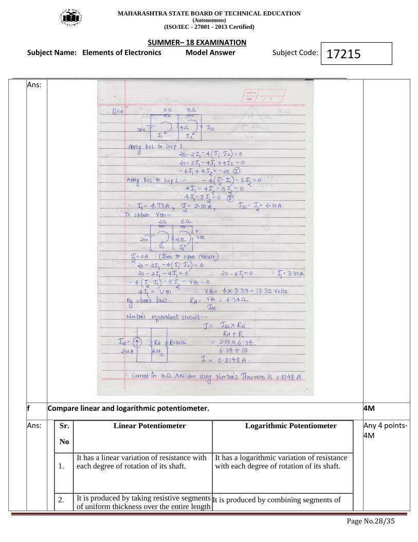
e Calculate the value of current in 10 Ω resistor using Norton's Theorem. (refer fig. 5)
4M
MAHARASHTRA STATE BOARD OF TECHNICAL EDUCATION (Autonomous)
(ISO/IEC - 27001 - 2013 Certified)
SUMMER– 18 EXAMINATION Subject Name: Elements of Electronics Model Answer Subject Code:
__________________________________________________________________________________________________
Page No.28/35
17215
Ans:
f Compare linear and logarithmic potentiometer. 4M
Ans:
Sr. Linear Potentiometer Logarithmic Potentiometer
No
1. It has a linear variation of resistance with each degree of rotation of its shaft.
It has a logarithmic variation of resistance with each degree of rotation of its shaft.
2. It is produced by taking resistive segments of uniform thickness over the entire length
It is produced by combining segments of
Any 4 points-4M
MAHARASHTRA STATE BOARD OF TECHNICAL EDUCATION (Autonomous)
(ISO/IEC - 27001 - 2013 Certified)
SUMMER– 18 EXAMINATION Subject Name: Elements of Electronics Model Answer Subject Code:
__________________________________________________________________________________________________
Page No.29/35
17215
of the segment.
resistance mixers having different
resistivity to make up the total length of the
film.
3.
Linear potentiometers are less expensive as compared to logarithmic potentiometers.
Logarithmic potentiometers are more expensive as compared to linear potentiometers.
4 In consumer electronics, user control uses Logarithmic potentiometers are often used in connection with audio amplifiers.
linear potentiometers.
Q. No.
Sub Q. N.
Answers Marking Scheme
6 Attempt any FOUR: 16- Total Marks
a Calculate value of capacitor if following is printed on body of capacitors : (i) 404 (ii) 2K3. 4M
Ans: Capacitor marking is “404” It’s mean that = 40 + 4 Zeros = 400000 pF = 400 nF
2K3 = 2.3k = (2.3 x 103) x 10-12 = 2.3 x 10-9 =2.3nF
b Describe the working of tunnel diode. Draw its characteristics. 4M
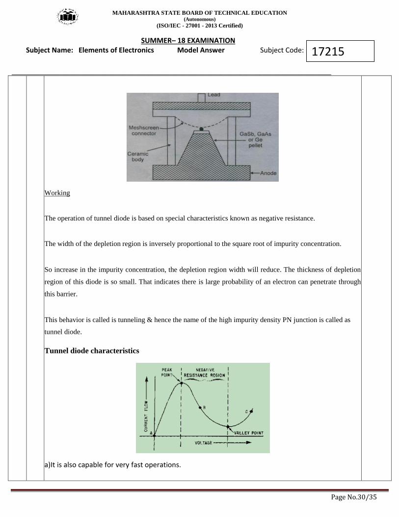
Ans: Symbol of TUNNEL DIODE
operating principle of tunnel diode
MAHARASHTRA STATE BOARD OF TECHNICAL EDUCATION (Autonomous)
(ISO/IEC - 27001 - 2013 Certified)
SUMMER– 18 EXAMINATION Subject Name: Elements of Electronics Model Answer Subject Code:
__________________________________________________________________________________________________
Page No.30/35
17215
Working
The operation of tunnel diode is based on special characteristics known as negative resistance.
The width of the depletion region is inversely proportional to the square root of impurity concentration.
So increase in the impurity concentration, the depletion region width will reduce. The thickness of depletion
region of this diode is so small. That indicates there is large probability of an electron can penetrate through
this barrier.
This behavior is called is tunneling & hence the name of the high impurity density PN junction is called as
tunnel diode.
Tunnel diode characteristics
a)It is also capable for very fast operations.
MAHARASHTRA STATE BOARD OF TECHNICAL EDUCATION (Autonomous)
(ISO/IEC - 27001 - 2013 Certified)
SUMMER– 18 EXAMINATION Subject Name: Elements of Electronics Model Answer Subject Code:
__________________________________________________________________________________________________
Page No.31/35
17215
b)It has heavily doped PN junction of only 10 nm wide .
c)It exhibit negative resistance region.
d)Applications:microwave applications,ultra high speed switching device,relaxation oscillators.
e)The process of penetrating charge carrier directly through potential barrier is called tunneling.
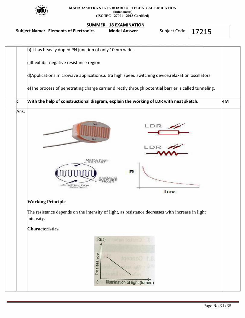
c With the help of constructional diagram, explain the working of LDR with neat sketch. 4M
Ans:
Working Principle
The resistance depends on the intensity of light, as resistance decreases with increase in light
intensity.
Characteristics
MAHARASHTRA STATE BOARD OF TECHNICAL EDUCATION (Autonomous)
(ISO/IEC - 27001 - 2013 Certified)
SUMMER– 18 EXAMINATION Subject Name: Elements of Electronics Model Answer Subject Code:
__________________________________________________________________________________________________
Page No.32/35
17215
Applications of LDR
1. They are often used as light sensors.
2. They are used when there is a need to detect absences or presences of light like in a camera light
meter.
3. Used in street lamps, alarm clock, burglar alarm circuits, light intensity meters,
for counting the packages moving on a conveyor belt, etc.
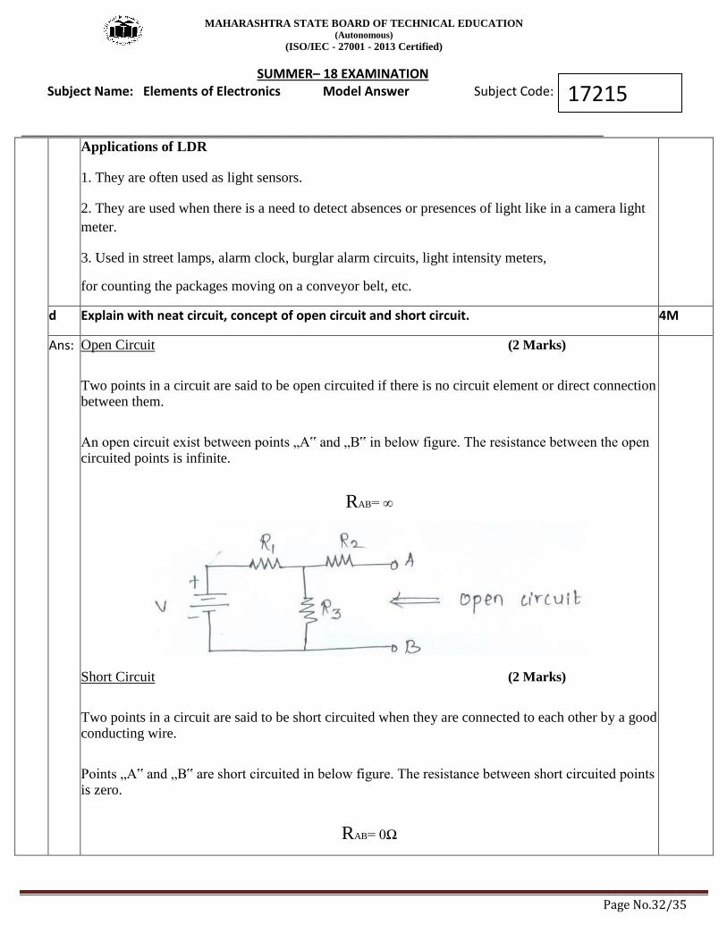
d Explain with neat circuit, concept of open circuit and short circuit. 4M
Ans: Open Circuit (2 Marks)
Two points in a circuit are said to be open circuited if there is no circuit element or direct connection between them.
An open circuit exist between points „A‟ and „B‟ in below figure. The resistance between the open circuited points is infinite.
RAB= ∞
Short Circuit (2 Marks)
Two points in a circuit are said to be short circuited when they are connected to each other by a good conducting wire.
Points „A‟ and „B‟ are short circuited in below figure. The resistance between short circuited points is zero.
RAB= 0Ω
MAHARASHTRA STATE BOARD OF TECHNICAL EDUCATION (Autonomous)
(ISO/IEC - 27001 - 2013 Certified)
SUMMER– 18 EXAMINATION Subject Name: Elements of Electronics Model Answer Subject Code:
__________________________________________________________________________________________________
Page No.33/35
17215
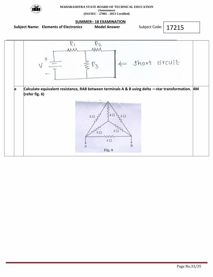
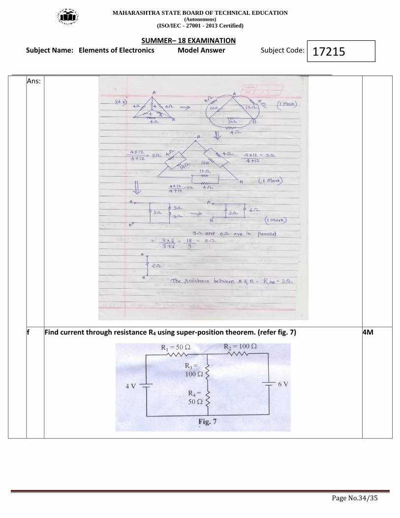
e Calculate equivalent resistance, RAB between terminals A & B using delta —star transformation. (refer fig. 6)
4M
MAHARASHTRA STATE BOARD OF TECHNICAL EDUCATION (Autonomous)
(ISO/IEC - 27001 - 2013 Certified)
SUMMER– 18 EXAMINATION Subject Name: Elements of Electronics Model Answer Subject Code:
__________________________________________________________________________________________________
Page No.34/35
17215
Ans:
f Find current through resistance R4 using super-position theorem. (refer fig. 7)
4M
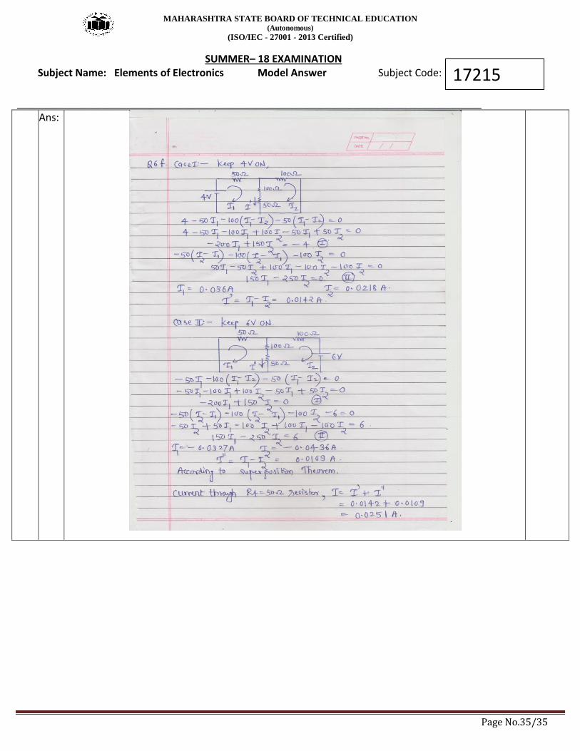
MAHARASHTRA STATE BOARD OF TECHNICAL EDUCATION (Autonomous)
(ISO/IEC - 27001 - 2013 Certified)
SUMMER– 18 EXAMINATION Subject Name: Elements of Electronics Model Answer Subject Code:
__________________________________________________________________________________________________
Page No.35/35
17215
Ans:
Related Documents


