Department of Electronics and Communication Engineering, Manipal Institute of Technology, Manipal, INDIA Subject Code : ECE – 101/102 BASIC ELECTRONICS COURSE MATERIAL For 1st & 2nd Semester B.E. (Revised Credit System) DEPARTMENT OF ELECTRONICS & COMMUNICATION ENGINEERING

Subject Code : ECE – 101/102 BASIC ELECTRONICS COURSE MATERIAL For 1st & 2nd Semester B.E.
Dec 31, 2015
Subject Code : ECE – 101/102 BASIC ELECTRONICS COURSE MATERIAL For 1st & 2nd Semester B.E. (Revised Credit System) DEPARTMENT OF ELECTRONICS & COMMUNICATION ENGINEERING. Zener diode is heavily doped P-N junction diode Designed to operate in reverse breakdown region - PowerPoint PPT Presentation
Welcome message from author
This document is posted to help you gain knowledge. Please leave a comment to let me know what you think about it! Share it to your friends and learn new things together.
Transcript

Department of Electronics and Communication Engineering,Manipal Institute of Technology, Manipal, INDIA
Subject Code : ECE – 101/102
BASIC ELECTRONICS
COURSE MATERIALFor
1st & 2nd Semester B.E.(Revised Credit System)
DEPARTMENT OF ELECTRONICS & COMMUNICATION ENGINEERING

Department of Electronics and Communication Engineering,Manipal Institute of Technology, Manipal, INDIA
Zener Diode
• Zener diode is heavily doped P-N junction diode
• Designed to operate in reverse breakdown region
• Each zener diode has specific breakdown voltage (VZ). Value of VZ depends on doping level
• Zener diodes are available with VZ ranging from 1.8V to 200V, power ratings from 250mW to 50W
• Symbol of zener diode:
Anode Cathode
P N

Zener diode
Department of Electronics and Communication Engineering,Manipal Institute of Technology, Manipal, INDIA

Department of Electronics and Communication Engineering,Manipal Institute of Technology, Manipal, INDIA
Zener Diode characteristics
• V-I characteristics:
VZ
IZK
IZM
I
V

Department of Electronics and Communication Engineering,Manipal Institute of Technology, Manipal, INDIA
Zener Diode characteristics• V-I characteristics:
– When zener diode is forward biased, it acts like ordinary diode – i.e., until certain voltage Vγ is reached, current is zero, then afterwards, current rises exponentially
– When zener diode is reverse biased, until the breakdown voltage is reached, current is zero or negligible
– When reverse voltage equals zener voltage, current rises exponentially in reverse direction
– After the breakdown has occurred, voltage across zener diode remains almost constant at VZ, only the current increases with the increase in applied reverse bias
Department of Electronics and Communication Engineering,Manipal Institute of Technology, Manipal, INDIA
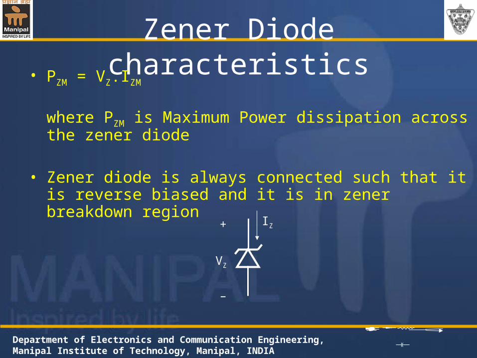
Zener Diode characteristics• PZM = VZ.IZM
where PZM is Maximum Power dissipation across the zener diode
• Zener diode is always connected such that it is reverse biased and it is in zener breakdown region
VZ
+
–
IZ

Department of Electronics and Communication Engineering,Manipal Institute of Technology, Manipal, INDIA
Zener Diode characteristics
• Equivalent circuits of zener diode
Forward ReverseBreakdown
• Note: RZ is usually very small, hence it can be neglected
Vγ
RFRR ≈ RZ
VZ
–
+ –
+N
P
N N N
P P P

Department of Electronics and Communication Engineering,Manipal Institute of Technology, Manipal, INDIA
Zener diode circuit• Analysis of networks employing zener diodes is similar to
analysis of ordinary diodes
• First, the state of the diode (ON, OFF or breakdown) must be determined, followed by substitution of correct model
• Figure shows a simple circuit employing a zener diode
RL VoVZ
+
–
+
–
Vi
RS ILIZIR
Department of Electronics and Communication Engineering,Manipal Institute of Technology, Manipal, INDIA
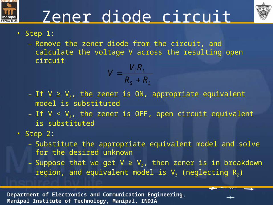
Zener diode circuit• Step 1:
– Remove the zener diode from the circuit, and calculate the voltage V across the resulting open circuit
– If V ≥ VZ, the zener is ON, appropriate equivalent model is substituted
– If V < VZ, the zener is OFF, open circuit equivalent is substituted
• Step 2:
– Substitute the appropriate equivalent model and solve for the desired unknown
– Suppose that we get V ≥ VZ, then zener is in breakdown region, and equivalent model is VZ (neglecting RZ)
LS
Li
RR
RVV

Department of Electronics and Communication Engineering,Manipal Institute of Technology, Manipal, INDIA
Zener diode circuit
IZ = ( IR – IL) where,
RL VoVZ
+
–
+
–
Vi
RS ILIZIR
S
ZiR R
VVI
L
oL R
VI
Zo VV , ,

Department of Electronics and Communication Engineering,Manipal Institute of Technology, Manipal, INDIA
Zener diode circuitProblem:
For the zener network, Vi= 16 V, RS= 1 K ohm, VZ= 10 V and RL= 3K ohm. Determine Vo, IZ and PZ .
Repeat for RL= 1.2K ohm
RL VoVZ
+
–
+
–
Vi
RS ILIZIR

Department of Electronics and Communication Engineering,Manipal Institute of Technology, Manipal, INDIA
Line Regulation
• Line Regulation is the capability to maintain a constant output voltage level on the output channel of the power supply despite the changes in the input voltage level
Problem on Line regulation
In a Zener network, RS = 120Ω, RL = 250Ω and VZ = 5V. Find the minimum and maximum current flowing through zener when input varies from 9V to 15V.

Department of Electronics and Communication Engineering,Manipal Institute of Technology, Manipal, INDIA
Load Regulation
• Load regulation is the capability to maintain a constant voltage level on the output channel of the power supply despite the changes in the load
Problem on Load regulation
For a Zener network, RS = 10Ω, VZ = 10V, Vi = 25V. Find the minimum and maximum current through zener when RL is varied between 10Ω and 100Ω

Department of Electronics and Communication Engineering,Manipal Institute of Technology, Manipal, INDIA
End of module 5
Related Documents


![SYLLABUS FOR ECE Syllabus.pdf[SYLLABUS FOR ECE] UNIVERSITY OF JAMMU FOR EXAMINATIONS TO BE HELD IN DECEMBER 2010 ONWARDS CLASS : B.E. IST SEMESTER BRANCH: COMMON TO ALL COURSE TITLE:](https://static.cupdf.com/doc/110x72/60a60dfd57a3bc62aa7edbe5/syllabus-for-ece-syllabuspdf-syllabus-for-ece-university-of-jammu-for-examinations.jpg)


