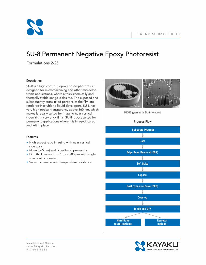
TECHNICAL DATA SHEET www.kayakuAM.com [email protected] 617-965-5511 Description SU-8 is a high contrast, epoxy based photoresist designed for micromachining and other microelec- tronic applications, where a thick chemically and thermally stable image is desired. The exposed and subsequently crosslinked portions of the film are rendered insoluble to liquid developers. SU-8 has very high optical transparency above 360 nm, which makes it ideally suited for imaging near vertical sidewalls in very thick films. SU-8 is best suited for permanent applications where it is imaged, cured and left in place. Features • High aspect ratio imaging with near vertical side walls • i-Line (365 nm) and broadband processing • Film thicknesses from 1 to > 200 μm with single spin coat processes • Superb chemical and temperature resistance SU-8 Permanent Negative Epoxy Photoresist Formulations 2-25 MEMS gears with SU-8 removed Substrate Pretreat Coat Edge Bead Removal (EBR) Soft Bake Expose Post Exposure Bake (PEB) Develop Rinse and Dry Hard Bake (cure) optional Removal optional Process Flow

Welcome message from author
This document is posted to help you gain knowledge. Please leave a comment to let me know what you think about it! Share it to your friends and learn new things together.
Transcript
T E C H N I C A L D ATA S H E E T
w w w. k a y a k u A M . c o m s a l e s @ k a y a k u A M . c o m 6 1 7 - 9 6 5 - 5 5 1 1
Description
SU-8 is a high contrast, epoxy based photoresist designed for micromachining and other microelec-tronic applications, where a thick chemically and thermally stable image is desired. The exposed and subsequently crosslinked portions of the film are rendered insoluble to liquid developers. SU-8 has very high optical transparency above 360 nm, which makes it ideally suited for imaging near vertical sidewalls in very thick films. SU-8 is best suited for permanent applications where it is imaged, cured and left in place.
Features
• High aspect ratio imaging with near vertical side walls• i-Line (365 nm) and broadband processing • Film thicknesses from 1 to > 200 μm with single spin coat processes• Superb chemical and temperature resistance
SU-8 Permanent Negative Epoxy PhotoresistFormulations 2-25
MEMS gears with SU-8 removed
Substrate Pretreat
Coat
Edge Bead Removal (EBR)
Soft Bake
Expose
Post Exposure Bake (PEB)
Develop
Rinse and Dry
Hard Bake (cure) optional
Removal optional
Process Flow
T E C H N I C A L D ATA S H E E T
w w w. k a y a k u A M . c o m s a l e s @ k a y a k u A M . c o m 6 1 7 - 9 6 5 - 5 5 1 1
PROCESSING GUIDELINESSU-8 is most commonly processed with convention-al i-Line and broadband (350–450 nm) radiation, although it may be imaged with e-beam or X-ray. I-Line (365 nm) is recommended. Upon exposure, crosslinking proceeds in two steps (1) formation of a strong acid during the exposure process, followed by (2) acid-initiated, thermally driven epoxy crosslinking during the post exposure bake (PEB) step.
A normal process is: spin coat, soft bake, expose, post expose bake (PEB) and develop. A controlled hard bake may be required to further crosslink the imaged SU-8 structures when they will remain as part of the device. The entire process should be opti-mized for the specific application. A baseline process is given here to be used as a starting point.
Substrate Preparation
To obtain maximum process reliability, substrates should be clean and dry prior to applying the SU-8 resist. Start with a solvent cleaning or a rinse with dilute acid, followed by a DI water rinse. Where ap-plicable, substrates should be subjected to a piranha etch/clean (H2SO4 & H2O2). To dehydrate the surface, bake at 200°C for 5 minutes on a hotplate. For appli-cations that require electroplating and subsequent removal of SU-8 apply Kayaku Advanced Materials’ OmniCoat prior to processing SU-8.
Coat
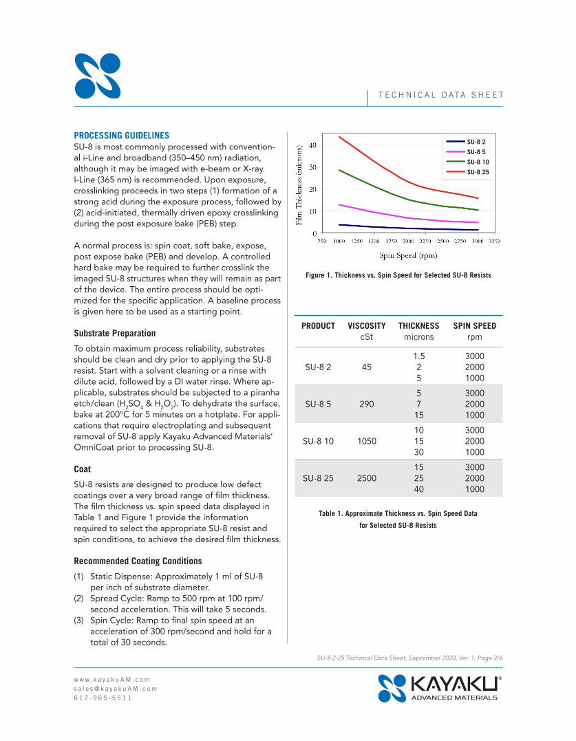
SU-8 resists are designed to produce low defect coatings over a very broad range of film thickness. The film thickness vs. spin speed data displayed in Table 1 and Figure 1 provide the information required to select the appropriate SU-8 resist and spin conditions, to achieve the desired film thickness.
Recommended Coating Conditions
(1) Static Dispense: Approximately 1 ml of SU-8 per inch of substrate diameter.(2) Spread Cycle: Ramp to 500 rpm at 100 rpm/ second acceleration. This will take 5 seconds.(3) Spin Cycle: Ramp to final spin speed at an acceleration of 300 rpm/second and hold for a total of 30 seconds.
SU-8 2-25 Technical Data Sheet, September 2020, Ver. 1, Page 2/6
PRODUCT VISCOSITY THICKNESS SPIN SPEED cSt microns rpm
1.5 3000 SU-8 2 45 2 2000 5 1000
5 3000 SU-8 5 290 7 2000 15 1000
10 3000 SU-8 10 1050 15 2000 30 1000
15 3000 SU-8 25 2500 25 2000 40 1000
Table 1. Approximate Thickness vs. Spin Speed Data
for Selected SU-8 Resists
Figure 1. Thickness vs. Spin Speed for Selected SU-8 Resists
SU-8 2
SU-8 5
SU-8 10
SU-8 25

T E C H N I C A L D ATA S H E E T
w w w. k a y a k u A M . c o m s a l e s @ k a y a k u A M . c o m 6 1 7 - 9 6 5 - 5 5 1 1
Soft Bake
After the resist has been applied to the substrate, it must be soft baked to evaporate the solvent and densify the film. SU-8 is normally baked on a level hot plate, although convection ovens may be used for thin films. The following bake times are based on contact hot plate processes. Bake times should be optimized for proximity and convection oven bake processes since solvent evaporation rate is influ-enced by the rate of heat transfer and ventilation.
For best results, ramping or stepping the soft bake temperature is recommended. Lower initial bake temperatures allow the solvent to evaporate out of the film at a more controlled rate, resulting in better coating fidelity, reduced edge bead and better resist-to-substrate adhesion. Refer to Table 2 for two step contact hot plate process recommendations.
PRODUCT THICKNESS SOFTBAKE TIME microns minutes @ 65ºC minutes @ 95ºC
1.5 1 1 SU-8 2 2 1 3 5 1 3
5 1 3 SU-8 5 7 2 5 15 2 7–10
10 2 5–7 SU-8 10 15 2 7–10 30 3 5–15
15 2 7–10 SU-8 25 25 3 10–15 40 5 15
Table 2. Recommended Soft Bake Parameters
SU-8 2-25 Technical Data Sheet, September 2020, Ver. 1, Page 3/6
Exposure
SU-8 is optimized for i-Line and broadband (350–450 nm) exposure. i-Line exposure tools are recommend-ed. SU-8 is virtually transparent and insensitive above 375 nm, but has high actinic absorption below 350 nm. This can be seen in Figure 2. Excessive dose below 350 nm may, results in over exposure of the top portion of the resist film, causing exaggerated negative sidewall profiles or T-topping. The optimal exposure dose will depend on film thickness (thicker films require higher dosage) and process parameters. The exposure dose recommendations in Figure 3 are based on source intensity measurements taken with an i-Line (365 nm) radiometer and probe.
Expose tip: When using a broad spectral output source, for best imaging results, i.e. straightest side-walls, filter out excessive energy below 350 nm.
Catastrophic adhesion failure and excessive cracking often indicate an under crosslinking condition. To correct the problem, increase the exposure dose and/or increase the post exposure bake (PEB) time.
Figure 2. SU-8 Absorbance vs. Wavelength
for Various Film Thicknesses

T E C H N I C A L D ATA S H E E T
w w w. k a y a k u A M . c o m s a l e s @ k a y a k u A M . c o m 6 1 7 - 9 6 5 - 5 5 1 1
Post Exposure Bake (PEB)
Following exposure, a post expose bake (PEB) must be performed to selectively crosslink the exposed portions of the film. This bake can be performed either on a hot plate or in a convection oven though hotplates are recommended. Optimum crosslink density is obtained through careful adjustments of the exposure and PEB process conditions. The bake recommendations below are based on results ob-tained with a contact hot plate.
PEB tip: SU-8 is readily crosslinked and can result in a highly stressed film. To minimize stress, wafer bowing and resist cracking, a slow ramp or two step contact hot plate process is recommended, as shown in Table 3. Rapid cooling after PEB should be avoided.
PRODUCT THICKNESS PEB TIME microns minutes@65ºC minutes@95ºC
1.5 1 1 SU-8 2 2 1 1 5 1 1 5 1 1 SU-8 5 7 1 1 15 1 2 10 1 2 SU-8 10 15 1 2 30 1 3 15 1 2 SU-8 25 25 1 3 40 1 4
Develop
SU-8 resists have been optimized for use with Kayaku Advanced Materials’ SU-8 Developer. Immersion, spray or spray-puddle processes can be used. Other solvent based developers such as ethyl lactate and diacetone alcohol may also be used. Strong agita-tion is recommended for high aspect ratio and/or thick film structures. Recommended develop times are given in Table 4 for immersion processes. These proposed develop times are approximate, since actual dissolution rates can vary widely as a function of agitation rate, temperature and resist processing parameters.
PRODUCT THICKNESS DEVELOPMENT TIME microns minutes
1.5 1 SU-8 2 2 1 5 1 5 1 SU-8 5 7 1 15 3 10 2 SU-8 10 15 3 30 5 15 3 SU-8 25 25 4 40 6
Table 4. Recommended Develop Processes
Rinse and Dry
Following development with SU-8 Developer, spray rinse with fresh developer then dry with a gentle stream of filtered pressurized air or nitrogen.
Figure 3. Exposure Dose
Table 3. Recommended Post Exposure Bake Parameters
Film Thickness (μm)
Exp
osur
e E
nerg
y (m
J/cm
2 ) Exposure Range
Upper limit
Lower limit
SU-8 2-25 Technical Data Sheet, September 2020, Ver. 1, Page 4/6

T E C H N I C A L D ATA S H E E T
w w w. k a y a k u A M . c o m s a l e s @ k a y a k u A M . c o m 6 1 7 - 9 6 5 - 5 5 1 1
SU-8 2-25 Technical Data Sheet, September 2020, Ver. 1, Page 5/6
Hard Bake (cure)
SU-8 has good mechanical properties, therefore hard bakes are normally not required. For applications where the imaged resist is to be left as part of the final device, the resist may be ramp/step hard baked at 150°C on a hot plate or in a convection oven to further crosslink the material. Bake times vary based on type of bake process and film thickness.
Removal
After exposure and PEB, SU-8 is a highly crosslinked epoxy, which makes it extremely difficult to remove with conventional solvent based resist strippers. Kayaku Advanced Materials’ Remover PG will swell and lift off minimally crosslinked SU-8.
However, if OmniCoat has been applied, immersion in Remover PG should effect a clean and thorough lift-off of the SU-8 Material. It will not remove fully cured or hard baked SU-8 without the use of Omni-Coat. Alternate removal processes include immersion in oxidizing acid solutions such as piranha etch/clean, plasma ash (see conditions below), RIE, laser ablation and pyrolosis.
To remove minimally crosslinked SU-8, or if using OmniCoat, with Remover PG, heat the bath to 50–80°C and immerse the substrates for 30–90 minutes. Actual strip time will depend on resist thickness and crosslink density.
For more information on Kayaku Advanced Materials’ OmniCoat and Remover PG, please see the relevant product data sheets.
PLASMA REMOVAL
Plasma removal conditions are: RIE 200W, 80 sccm O2, 8 sccm CF4, 100 mTorr, 10°C. For more information, refer to the SU-8 / KMPR® Removal applications note on the website www.kayakuAM.com. Also see www.r3t.de or www.tepla.com for microwave plasma tools for high throughput without damaging other micro-structures.
Storage
Store SU-8 resists upright in tightly closed containers in a cool, dry environment away from direct sunlight at a temperature of 40–70°F (4–21°C). Store away from light, acids, heat and sources of ignition. Shelf life is thirteen months from date of manufacture.
Disposal
The material and its container must be disposed in accordance with all local, state, federal and/or international regulations.
Handling
Consult Safety Data Sheet (SDS) for details on the handling procedures and product hazards prior to use. If you have any questions regarding handling precautions or product hazards, please email [email protected].
Disclaimer
Notwithstanding anything to the contrary contained in any sales documentation, e.g., purchase order forms, all sales are made on the following conditions:
All information contained in any Kayaku Advanced Materials, Inc. product literature reflects our current knowledge on the subject and is, we believe, re-liable. It is offered solely to provide possible sug-gestions for the customer’s own experiments and is not a substitute for any testing by the customer to determine the suitability of any of Kayaku Advanced Materials, Inc. products for any particular purpose. This information may be subject to revision as new knowledge and experience becomes available, but Kayaku Advanced Materials, Inc. assumes no obliga-tion to update or revise any data previously furnished to a customer; and if currency of data becomes an issue, the customer should contact Kayaku Advanced Materials, Inc. requesting updates. Since Kayaku Ad-vanced Materials, Inc. cannot anticipate all variations in actual end uses or in actual end-use conditions, it makes no claims, representations or warranties, express or implied including, without limitation any warranty of merchantability or fitness for a particular

T E C H N I C A L D ATA S H E E T
w w w. k a y a k u A M . c o m s a l e s @ k a y a k u A M . c o m 6 1 7 - 9 6 5 - 5 5 1 1
purpose; and the customer waives all of the same. Kayaku Advanced Materials, Inc. expressly disclaims any responsibility or liability and assumes no respon-sibility or liability in connection with any use of this information including, without limitation, any use, handling, storage or possession of any Kayaku Advanced Materials, Inc. products, or the applica-tion of any process described herein or the results desired or anything relating to the design of the customer’s products. Nothing in this publication is to be considered as a license to operate under or a recommendation to infringe any patent right.
SU-8 2-25 Technical Data Sheet, September 2020, Ver. 1, Page 6/6

T E C H N I C A L D ATA S H E E T
w w w. k a y a k u A M . c o m s a l e s @ k a y a k u A M . c o m 6 1 7 - 9 6 5 - 5 5 1 1
Description
SU-8 is a high contrast, epoxy based photoresist designed for micromachining and other microelec-tronic applications where a thick chemically and thermally stable image is desired. The exposed and subsequently crosslinked portions of the film are rendered insoluble to liquid developers. SU-8 has very high optical transparency above 360 nm which makes it ideally suited for imaging near vertical sidewalls in very thick films. SU-8 is best suited for permanent applications where it is imaged, cured and left in place.
Features
• High aspect ratio imaging with near vertical sidewalls• i-Line (365 nm) and broadband processing • Film thicknesses from 1 to > 200 μm with single spin coat processes• Superb chemical and temperature resistance
SU-8 Permanent Negative Epoxy PhotoresistFormulations 50–100
MEMS gears with SU-8 removed
Substrate Pretreat
Coat
Edge Bead Removal (EBR)
Soft Bake
Expose
Post Exposure Bake (PEB)
Develop
Rinse and Dry
Hard Bake (cure) optional
Removal optional
Process Flow
T E C H N I C A L D ATA S H E E T
w w w. k a y a k u A M . c o m s a l e s @ k a y a k u A M . c o m 6 1 7 - 9 6 5 - 5 5 1 1
PROCESSING GUIDELINESSU-8 is most commonly processed with conventional near UV (350–450 nm) radiation, although it may be imaged with e-beam or X-ray. i-Line (365 nm) is recommended. Upon exposure, crosslinking proceeds in two steps (1) formation of a strong acid during the exposure process, followed by (2) acid- initiated, thermally driven epoxy crosslinking during the post exposure bake (PEB) step.
A normal process is: spin coat, soft bake, expose, post expose bake (PEB) and develop. A controlled hard bake is recommended to further crosslink the imaged SU-8 structures when they will remain as part of the device. The entire process should be optimized for the specific application. A baseline process is given here to be used as a starting point.
Substrate Preparation
To obtain maximum process reliability, substrates should be clean and dry prior to applying the SU-8 resist. Start with a solvent cleaning, or a rinse with dilute acid, followed by a DI water rinse. Where ap-plicable, substrates should be subjected to a piranha etch/clean (H2SO4 & H2O2) To dehydrate the surface, bake at 200ºC for 5 minutes on a hotplate. For appli-cations that require electroplating and subsequent removal of SU-8, apply OmniCoat prior to processing SU-8.
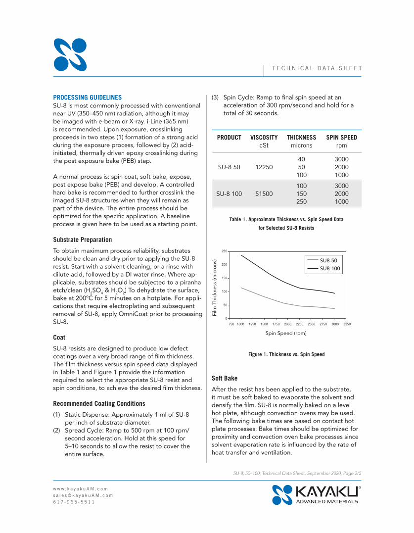
Coat
SU-8 resists are designed to produce low defect coatings over a very broad range of film thickness. The film thickness versus spin speed data displayed in Table 1 and Figure 1 provide the information required to select the appropriate SU-8 resist and spin conditions, to achieve the desired film thickness.
Recommended Coating Conditions
(1) Static Dispense: Approximately 1 ml of SU-8 per inch of substrate diameter.(2) Spread Cycle: Ramp to 500 rpm at 100 rpm/ second acceleration. Hold at this speed for 5–10 seconds to allow the resist to cover the entire surface.
SU-8, 50–100, Technical Data Sheet, September 2020, Page 2/5
Table 1. Approximate Thickness vs. Spin Speed Data
for Selected SU-8 Resists
Figure 1. Thickness vs. Spin Speed
(3) Spin Cycle: Ramp to final spin speed at an acceleration of 300 rpm/second and hold for a total of 30 seconds.
Soft Bake
After the resist has been applied to the substrate, it must be soft baked to evaporate the solvent and densify the film. SU-8 is normally baked on a level hot plate, although convection ovens may be used. The following bake times are based on contact hot plate processes. Bake times should be optimized for proximity and convection oven bake processes since solvent evaporation rate is influenced by the rate of heat transfer and ventilation.
PRODUCT VISCOSITY THICKNESS SPIN SPEED cSt microns rpm
40 3000 SU-8 50 12250 50 2000 100 1000
100 3000 SU-8 100 51500 150 2000 250 1000

T E C H N I C A L D ATA S H E E T
w w w. k a y a k u A M . c o m s a l e s @ k a y a k u A M . c o m 6 1 7 - 9 6 5 - 5 5 1 1
SU-8, 50–100, Technical Data Sheet, September 2020, Page 3/5
For best results, ramping or stepping the soft bake temperature is recommended. Lower initial bake temperatures allow the solvent to evaporate out of the film at a more controlled rate, which results in better coating fidelity, reduced edge bead and better resist-to-substrate adhesion. Refer to Table 2 for two-step contact hot plate process recom- mendations.
PRODUCT THICKNESS SOFT BAKE TIME microns minutes @ 65ºC minutes @ 95ºC
40 5 15 SU-8 50 50 6 20 100 10 30
100 10 30 SU-8 100 150 20 50 250 30 90
Table 2. Recommended Soft Bake Parameters
Exposure
SU-8 is optimized for near UV (350–450 nm) expo-sure. i-Line exposure tools are recommended. SU-8 is virtually transparent and insensitive above 400 nm but has high actinic absorption below 350 nm. This can be seen in Figure 2. Excessive dose below 350 nm may, therefore, result in over exposure of the top portion of the resist film, resulting in exaggerated negative sidewalI profiles or T-topping. The optimal exposure dose will depend on film thickness (thicker films require higher dosage) and process parameters. The exposure dose recommendations in Table 3 are based on source intensity measurements taken with an i-Line (365 nm) radiometer and probe.
Exposure Tip: When using a broad spectral output source, for best imaging results, i.e. straightest side-walls, filter out excessive energy below 350 nm.
Catastrophic adhesion failure and excessive cracking often indicate an under crosslinking condition. To correct the problem, increase the exposure dose and/
or increase the post exposure bake (PEB) time.
Figure 2. SU-8 Absorbance vs. Film Thickness
Figure 3. Exposure Dose
Film Thickness (μm)
Exp
osu
re E
nerg
y (m
J/cm
2 ) Exposure Range
Upper limit
Lower limit
T E C H N I C A L D ATA S H E E T
w w w. k a y a k u A M . c o m s a l e s @ k a y a k u A M . c o m 6 1 7 - 9 6 5 - 5 5 1 1
Post Exposure Bake (PEB)
Following exposure, a post expose bake (PEB) must be performed to selectively crosslink the exposed portions of the film. This bake can be performed either on a hot plate or in a convection oven. Op-timum crosslink density is obtained through careful adjustments of the exposure and PEB process condi-tions. The bake recommendations below are based on results obtained with a contact hot plate.
PEB tip: SU-8 is readily crosslinked and can result in a highly stressed film. To minimize stress, wafer bowing and resist cracking, a slow ramp or two-step contact hot plate process is recommended, as shown in Table 4. Rapid cooling after PEB should be avoided.
SU-8, 50–100, Technical Data Sheet, September 2020, Page 4/5
Table 4. Recommended Post Exposure Bake Parameters
PRODUCT THICKNESS PEB TIME microns minutes@65ºC minutes@95ºC
40 1 4 SU-8 50 50 1 5 100 1 10
100 1 10 SU-8 100 150 1 12 200 1 20
Develop
SU-8 resists have been optimized for use with SU-8 Developer. Immersion, spray or spray-puddle pro-cesses can be used. Other solvent based developers such as ethyl lactate and diacetone alcohol may also be used. Strong agitation is recommended for high aspect ratio and/or thick film structures. Rec-ommended develop times are given in Table 5 for immersion processes. These proposed develop times are approxinrate, since actual dissolution rates can vary widely as a function of agitation rate, tempera-ture and resist processing parameters.
PRODUCT THICKNESS DEVELOPMENT TIME microns minutes
40 6 SU-8 50 50 6 100 10
100 10 SU-8 100 150 15 250 20
Rinse and Dry
Following development with SU-8 Developer, spray rinse with fresh developer then dry with a gentle stream of filtered pressurized air or nitrogen.
Hard Bake (cure)
SU-8 has good mechanical properties, therefore hard bakes are normally not required. For applications where the imaged resist is to be left as part of the final device, the resist may be ramp/step hard baked between 150–200°C on a hot plate or in a convec-tion oven to further crosslink the material. Bake times vary based on type of bake process and film thickness.
Removal
After exposure and PEB, SU-8 is a highly crosslinked epoxy, which makes it extremely difficult to remove with conventional solvent-based resist strippers. Kayaku Advanced Materials’ Remover PG will swell and lift off minimally crosslinked SU-8.
However, if OmniCoat has been applied, immersion in Remover PG should effect a clean and thorough lift-off of the SU-8 material. It will not remove fully cured or hard baked SU-8 without the use of Omni-Coat. Alternate removal processes include immersion in oxidizing acid solutions such as piranha etch/clean, plasma ash, RIE, laser ablation and pyrolosis.
To remove minimally crosslinked SU-8, or if using OmniCoat, with Remover PG, heat the bath to 50-
Table 5. Recommended Develop Processes

T E C H N I C A L D ATA S H E E T
w w w. k a y a k u A M . c o m s a l e s @ k a y a k u A M . c o m 6 1 7 - 9 6 5 - 5 5 1 1
SU-8, 50–100, Technical Data Sheet, September 2020, Page 5/5
80°C and immerse the substrates for 30–90 minutes. Actual strip time will depend on resist thickness and crosslink density. For more information on Kayaku Advanced Materials’ OmniCoat and Remover PG, please see the relevant product data sheets.
PLASMA REMOVAL
Plasma removal conditions are: RIE 200W, 80 sccm O2, 8 sccm CF4, 100 mTorr, 10°C. For more information, refer to the SU-8 / KMPR® Removal applications note on the website www.kayakuAM.com. Also see www.r3t.de or www.tepla.com for microwave plasma tools for high throughput without damaging other micro-structures.
Storage
Store SU-8 resists upright in tightly closed containers in a cool, dry environment away from direct sunlight at a temperature of 40-70°F (4–21°C). Store away from light, acids, heat and sources of ignition. Shelf life is thirteen months from date of manufacture.
Disposal
The material and its container must be disposed in accordance with all local, state, federal and/or international regulations.
Handling
Consult Safety Data Sheet (SDS) for details on thehandling procedures and product hazards prior touse. If you have any questions regarding handlingprecautions or product hazards, please [email protected].
Disclaimer
Notwithstanding anything to the contrary contained in any sales documentation, e.g., purchase order forms, all sales are made on the following conditions:
All information contained in any Kayaku Advanced Materials, Inc. product literature reflects our current knowledge on the subject and is, we believe, re-liable. It is offered solely to provide possible sug-gestions for the customer’s own experiments and is not a substitute for any testing by the customer to
determine the suitability of any of Kayaku Advanced Materials, Inc. products for any particular purpose. This information may be subject to revision as new knowledge and experience becomes available, but Kayaku Advanced Materials, Inc. assumes no obliga-tion to update or revise any data previously furnished to a customer; and if currency of data becomes an issue, the customer should contact Kayaku Advanced Materials, Inc. requesting updates. Since Kayaku Advanced Materials, Inc. cannot anticipate all variations in actual end uses or in actual end-use conditions, it makes no claims, representations or warranties, express or implied including, without lim-itation any warranty of merchantability or fitness for a particular purpose; and the customer waives all of the same. Kayaku Advanced Materials, Inc. expressly disclaims any responsibility or liability and assumes no responsibility or liability in connection with any use of this information including, without limitation, any use, handling, storage or possession of any Kayaku Advanced Materials, Inc. products, or the application of any process described herein or the results desired or anything relating to the design of the customer’s products. Nothing in this publication is to be considered as a license to operate under or a recommendation to infringe any patent right.
Related Documents