American Journal of Materials Science and Technology (2012) 1: 11-21 doi:10.7726/ajmst.2012.1002 Research Article ______________________________________________________________________________________________________________________________ *Corresponding authors: 1*Arts, Commerce and Science College, Borsad- 388540, Dist-Anand, Gujarat, India 2*Dr. Jivraj Mehta Institute of Technology, Mogar, Anand, Gujarat, India 3Department of Physics, Sardar Patel University, Vallabh Vidyanagar- 388 120, Gujarat, India 1E-mail: [email protected] 11 Structural and Surface Studies of Vacuum Evaporated Cadmium Telluride Thin Films H. S. Patel *1 , J. R. Rathod *2 , K. D. Patel 3 and V. M. Pathak 3 Received 17 July 2012; Published online 29 September 2012 © The author(s) 2012. Published with open access at uscip.org Abstract Cadmium Telluride (CdTe) is one of the most well established II–VI compounds largely due to its use as a photonic material. Existing applications, as well as those under consideration, are increasingly demanding stringent control of the material properties. The deposition of high quality thin films is of the utmost importance to such applications. This tendency has also manifested itself in the structural and surface morphology with higher structural perfection yielding smoother surfaces. The present investigations are about the structural and surface characterization of CdTe thin films. Thin films of CdTe with thickness around 4000Å have been deposited by the thermal evaporation method at room temperature. The structural characterization of this film was carried out using XRD (X-ray diffraction technique) and TEM (Transmission electron microscopy). The structure of CdTe film was found to be hexagonal. Also, the lattice parameters, grain size (D), dislocation density (ρ) and micro strain (ε), were taken from the XRD data. From TEM of CdTe thin films, the polycrystalline nature was confirmed. A surface morphology study was done by SEM (Scanning electron microscopy) technique. Atomic Force Microscopy (AFM) provides numerical data of surface height at digitized locations, which are usable for various surface characterizations. In this paper, the results have been analyzed to draw some conclusions which are also presented here. Keywords: Thin film, CdTe, XRD, TEM, SEM, AFM. 1. Introduction Cadmium telluride (CdTe) is a very interesting semiconductor in the form of thin films; it is one of the most promising polycrystalline materials (Wu Xuanzhi, 2004) for producing opto-electronic devices (Ebeid M. R. et al, 2005). The Schottky junction and heterojunction devices have also been investigated for understanding the charge transport mechanism (Kidi, D. and Touskova, 1988), device parameters and solar energy conversion (Basol. B.M., 1989; Macandless, B.E. and Birkmine, R.W., 1998).

Welcome message from author
This document is posted to help you gain knowledge. Please leave a comment to let me know what you think about it! Share it to your friends and learn new things together.
Transcript

American Journal of Materials Science and Technology (2012) 1: 11-21 doi:10.7726/ajmst.2012.1002 Research Article
______________________________________________________________________________________________________________________________ *Corresponding authors: 1*Arts, Commerce and Science College, Borsad- 388540, Dist-Anand, Gujarat, India 2*Dr. Jivraj Mehta Institute of Technology, Mogar, Anand, Gujarat, India 3Department of Physics, Sardar Patel University, Vallabh Vidyanagar- 388 120, Gujarat, India 1E-mail: [email protected]
11
Structural and Surface Studies of Vacuum Evaporated Cadmium
Telluride Thin Films
H. S. Patel*1, J. R. Rathod*2, K. D. Patel3and V. M. Pathak3 Received 17 July 2012; Published online 29 September 2012 © The author(s) 2012. Published with open access at uscip.org
Abstract Cadmium Telluride (CdTe) is one of the most well established II–VI compounds largely due to its use as a photonic material. Existing applications, as well as those under consideration, are increasingly demanding stringent control of the material properties. The deposition of high quality thin films is of the utmost importance to such applications. This tendency has also manifested itself in the structural and surface morphology with higher structural perfection yielding smoother surfaces. The present investigations are about the structural and surface characterization of CdTe thin films. Thin films of CdTe with thickness around 4000Å have been deposited by the thermal evaporation method at room temperature. The structural characterization of this film was carried out using XRD (X-ray diffraction technique) and TEM (Transmission electron microscopy). The structure of CdTe film was found to be hexagonal. Also, the lattice parameters, grain size (D), dislocation density (ρ) and micro strain (ε), were taken from the XRD data. From TEM of CdTe thin films, the polycrystalline nature was confirmed. A surface morphology study was done by SEM (Scanning electron microscopy) technique. Atomic Force Microscopy (AFM) provides numerical data of surface height at digitized locations, which are usable for various surface characterizations. In this paper, the results have been analyzed to draw some conclusions which are also presented here. Keywords: Thin film, CdTe, XRD, TEM, SEM, AFM.
1. Introduction Cadmium telluride (CdTe) is a very interesting semiconductor in the form of thin films; it is one of the most promising polycrystalline materials (Wu Xuanzhi, 2004) for producing opto-electronic devices (Ebeid M. R. et al, 2005). The Schottky junction and heterojunction devices have also been investigated for understanding the charge transport mechanism (Kidi, D. and Touskova, 1988), device parameters and solar energy conversion (Basol. B.M., 1989; Macandless, B.E. and Birkmine, R.W., 1998).

H. S. Patel, J. R. Rathod, K. D. Patel, V. M. Pathak/ American Journal of Materials Science and Technology (2012)
1: 11-21
12
The properties of the films generally depend on the structural parameters such as lattice constant, grain size, dislocation density, micro strain etc. which are dependent on the deposition conditions, e.g. rate of deposition, substrate temperature, vacuum conditions and the resultant film thickness. Scanning probe microscopes (SPM) define a broad group of instruments used to image and measure properties of materials, chemicals and biological surfaces. SPM images are obtained by scanning a sharp probe across a surface while monitoring and compiling the tip–sample interactions to provide an image. The two primary forms of SPM are scanning tunneling microscopy (STM) and atomic force microscopy (AFM) (Blanchard Cheryl R., 1996). In this case, the AFM is used to analyze the surface features of CdTe thin films prepared using the thermal evaporation technique. The AFM instrument produces two and three-dimensional images of the surface. Though AFM images are often used as micrographs of the surface, the data are also used to measure another important parameter such as surface roughness. Statistical measures of thin film surface roughness provide a more complete description of the surface than single valued parameters (Terry Andrew J. and Brown Christopher A., 1997). Two commonly used statistical measures of surface roughness are the bearing ratio and the power spectral density (PSD). The bearing ratio is a useful parameter for characterizing abrasive wear of the surfaces, (Terry Andrew J. and Brown Christopher A., 1997) and the PSD is the power spectrum of the Fourier transformation of the surface profile (Choi. Y. et al, 2001) which provides useful information on the geometrical structure of the surface. In particular, it is useful for detecting periodic structure in the profile. Here, the authors report their investigations on the evaluation of the above mentioned parameters along with the analysis of the surface photographs. This work investigated the structural properties and surface roughness of CdTe thin films prepared by the thermal evaporation method.
2. Experimental Thin films of 4000 Å were deposited at room temperature on chemically and ultrasonically cleaned and unheated glass substrates with the help of a vacuum coating unit (12A4D, HHV). All the gadgets of the vacuum chamber were cleaned first by acetone. A clean evaporation source (molybdenum boat) was fixed in the filament holder inside the chamber. CdTe powder having purity 99.99% was kept in the molybdenum boat. The glass substrates were cleaned by acetone and ultrasonic vibrations. The substrates were kept on the substrate holder and a crystal monitor was placed near it to measure the thickness in situ. The chamber was emptied at a pressure better than 10-5 torr by the combination of rotary and diffusion pumps. When a vacuum of 10-6 torr was attained in the vacuum chamber, the temperature of the boat was gradually raised to heat CdTe to temperatures greater than the melting point. This allowed the evaporation of CdTe material. The X-ray diffraction analysis of CdTe thin films has been carried out at 300K using Philips X-ray diffractometer, (model: X’PERT MPD Netherland) with CuKa radiation of wave length 1.54 Å. For TEM and SEM (XL -30, ESEM, Philips, Netherlands) studies, the films were deposited simultaneously on freshly cleaved NaCl crystals also. The morphology of thin film, together with that of glass substrate, was measured with an Atomic Force Microscope (AFM) operated in noncontact mode (for sample size 5µm × 5µm). Basically the
H. S. Patel, J. R. Rathod, K. D. Patel, V. M. Pathak/ American Journal of Materials Science and Technology (2012)
1: 11-21
13
AFM consists of the attainment of topographic images making probe scans over a surface in a surface plane, x-y, while the distance between the surface and the probe, is being controlled (Drake B. et al, 1987; Pitsch M. et al, 1989; Lifshin E., 1992; Stark Robert W., 2004).
3. Results and Discussion 3.1 XRD study of CdTe thinfilm Fig.1 shows the X-ray diffractogram of CdTe thin film.
Fig. 1. X – Ray Diffractogram of CdTe thin film at 4000 Å thickness.
The lattice parameters, a and c, were determined for a hexagonal structure using the following equation.
2 2 2
2 2 2
1 4
3
h hk k l
d a c
+ + = +
(1) where h, k and l represent the Miller indices and d is the inter planer spacing. The observed ‘d’ values and calculated ‘d’ values are shown in table 1.
Table 1: Structural parameter for CdTe thin film (h k l) Calculated
d - spacing (Å)
JCPDS d – spacing
(Å)
β2θ (degree)
Grain Size (nm)
Micro strain(ε)
(10-4)
Dislocation density (ρ)
(1015) (1 0 0) 3.9888 3.9800 0.2952 28.66 12.63 1.2174 (0 0 2) 3.7508 3.7500 0.3444 24.62 14.71 1.6494 (1 0 1) 3.5246 3.5200 0.2952 28.82 12.56 1.2036 (1 0 2) 2.7386 2.7350 0.3444 25.12 14.41 1.5842 (1 1 0) 2.2996 2.2950 0.3936 22.38 16.17 1.9951 (1 0 3) 2.1134 2.1150 0.3444 25.87 13.04 1.2986 (2 0 0) 1.9994 1.9950 0.3444 27.74 13.28 1.3459

H. S. Patel, J. R. Rathod, K. D. Patel, V. M. Pathak/ American Journal of Materials Science and Technology (2012)
1: 11-21
14
The lattice constants ‘a’ and ‘c’ are 4.55 Å and 7.4 Å; it is good agreement with the standard data file of JCPDS (1998. USA Card No. 19, 0193). The particle size (D) of the CdTe thin films was determined by using the Debye-Scherrer’s formula,
2cos
kD
θ
λ
β θ= (2)
where λ is the wave length of X –rays used, β is the FWHM, k is a constant (taken as 1) and θ is the angle between the incident and scattered X-rays (Moustafa, S.M., 2008).
The micro strain (ε) and the dislocation density (ρ) of the deposited films were evaluated using the equations
2co s
4
θβ θε = (3)
and 2
1
Dρ = (4)
The results of these calculations have also been shown in table 1. The data presented in table 1 matches with the earlier reports (J. G. Vazquez Luna et al, 1999; M. R. Ebeid et al, 2005; S. Deivanayaki et al, 2010) The results of these calculations have also been shown in table 1. The data presented in table 1 matches with the earlier reports (J. G. Vazquez Luna et al, 1999; M. R. Ebeid et al, 2005; S. Deivanayaki et al, 2010) 3.1 TEM STUDIES
The electron diffraction pattern for CdTe thin film is shown in fig 2. The nature of this diffraction pattern confirms the polycrystalline structure of the deposited films.
Fig. 2. Electro diffraction pattern of CdTe thin film of Thickness 4000 Å.
The wavelength of incident electron beam λ was calculated using the equation

H. S. Patel, J. R. Rathod, K. D. Patel, V. M. Pathak/ American Journal of Materials Science and Technology (2012)
1: 11-21
15
150
( )U Vλ =
(5) where U(v) is the acceleration potential in Volt. The accelerating potential of the electron beam used for these measurements was 200 kV. Substitution of this value in equation (5) yields λ to be around 0.0274 Å. Using the value of L (3 m) and the value of λ , the product λL was calculated and it was found to be 822 x 10-10cm2 . The diameter of the ring patterns were measured using a comparator. Substituting the values of the diameters of the rings and λL in equation (6) yields the value of inter planer spacing d as
2 Ld
diameter
λ=
(6) The d – values corresponding to all these rings have been calculated and are given in Table – 2. This Table also contains the d values obtained from the JCPDS data (1998. USA Card No. 19, 0193). The two values match and this confirms that the deposited CdTe films also possess the hexagonal structure (M.M. Al-Jassim et al, 2001).
Table 2: Results of TEM analysis for CdTe thin film for thickness 4.2 kÅ. Ring No.
Ring diameter D cm
Interplaner spacing d = 2λL/D Å
JCPDS d- values Å
(h k l)
1 4.1318 3.9788 3.9800 (1 0 0) 2 4.3947 3.7408 3.7500 (0 0 2) 3 4.6776 3.5146 3.5200 (1 0 1) 4 7.2117 2.2796 2.2950 (1 1 0)
3.3 SEM studies
The surface morphology of the as deposited CdTe thin film was observed in fig. 3 by scanning electron microscopy (SEM). From the micrographs, it shows that the film surfaces are dense and compact in nature. In the case of as deposited CdTe thin film, a few numbers of small size dots or pits were observed distributed randomly over the whole sample.
Fig. 3. SEM micrograph of CdTe thin film of 4000 Ǻ thickness.

H. S. Patel, J. R. Rathod, K. D. Patel, V. M. Pathak/ American Journal of Materials Science and Technology (2012)
1: 11-21
16
3.4 AFM studies
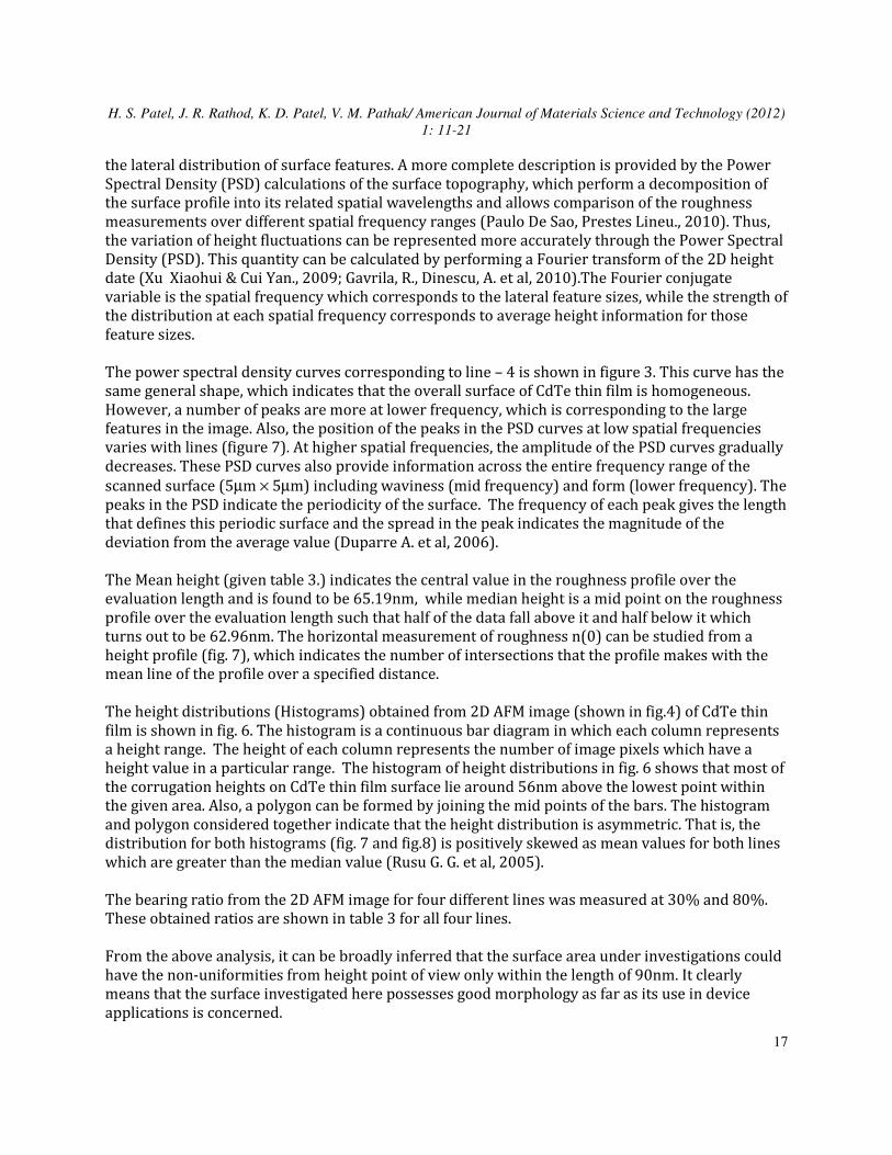
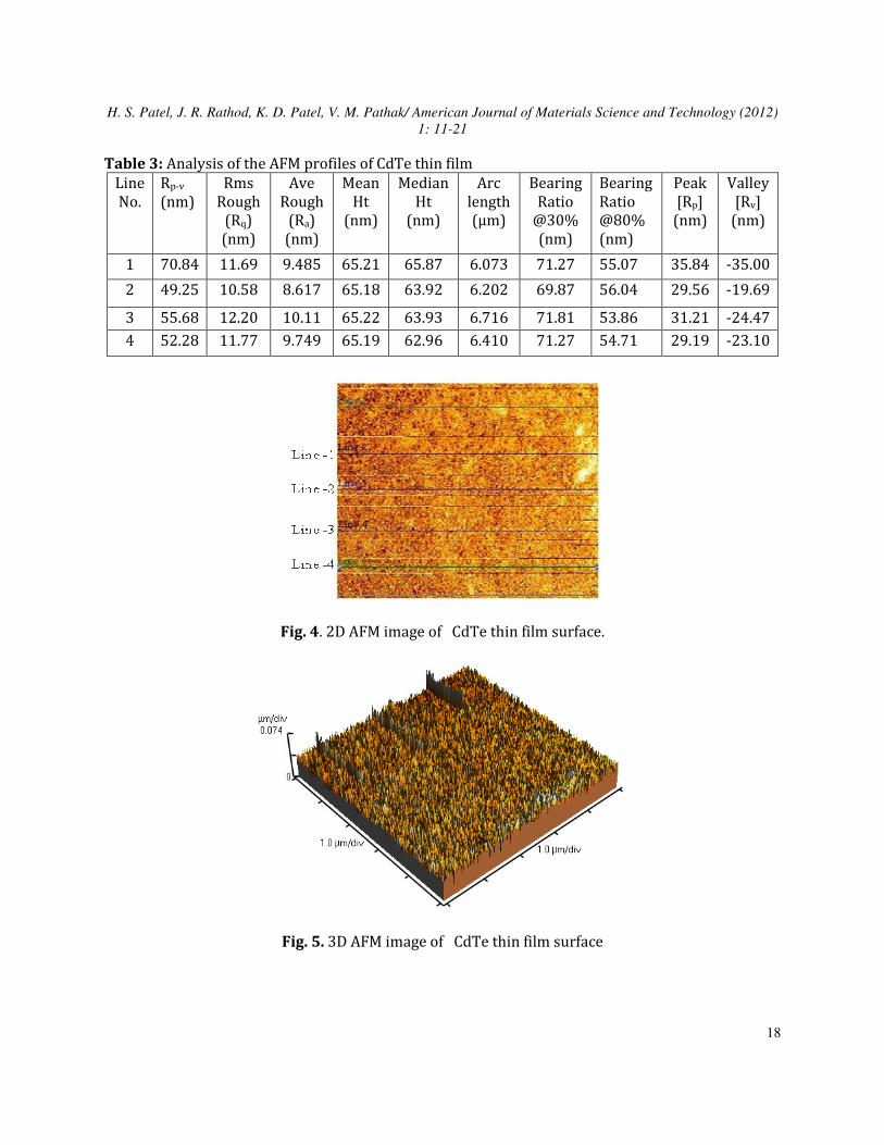
The as-grown polycrystalline CdTe thin film was viewed under the non-contact AFM mode. A silicon nitride tip was used to obtain topographic images of the surfaces of thin film. One can also obtain various line analyses spectrums from real images by the Digital Instruments 2SPM controller using di CP-II ProScan 1.9 software. Figures 4 and 5 show the 2D and 3D AFM images covering an area of 5µm × 5µm of CdTe thin film respectively. The images are computer generated, and the original data can be manipulated so that the surface of interest can be viewed from different directions. Distance scales in the x, y and z directions are marked on the 3D images and the z scale can be exaggerated as required. The 3D images (maximum 256 × 256 points) do make easier the visualization of the film surface. An image in a 3D format gives a rendition of what the surface topography actually looks like. That is, the data is displayed in the x y and z axes. Often the scale between the x, y and z axes is not equal. The surface features are very small in relationship to the x and y dimensions (as seen in fig.2) however, in 3D images, they look large (as seen in fig. 5). Fig. 5 shows that the surface possesses hilly (also valley) regions and is not an absolutely flat surface. These vertical features have a chemical composition different than the surrounding valleys (Shaheen Sean E. et al, 2001). The two dimensional image (shown in fig. 4) shows the x and y axes and contrast is used to depict the height of the image. An AFM image displayed in the 2D format looks much like an image obtained from a traditional microscope such as an optical microscope. To know the surface morphology of CdTe thin film, the line analysis is carried out in detail. The line profile is a two dimensional profile with a cross section extracted from an AFM image. This may be taken horizontally, vertically or at obtuse angles. The results of line analysis for CdTe thin film is given in table 3. A line trace of the surface profile along the chosen traverse length can be printed out together with the height profile, histogram, power spectrum, bearing ratio along with various statistical parameters as already mentioned earlier (table 3). The lines 1, 2, 3 and 4 (shown in fig. 6) have drawn on the surface of the thin film show indirectly the typical arrangement of the growth features in those regions. The height profiles taken along the horizontal lines 1, 2, 3 and 4 of the AFM image of CdTe thin film (shown in fig. 7) revealed the fact that the difference between the peak P and the valley z or v values (Rp-v) are 70.84nm, 49.25nm,55.68nm and 52.28nm of line – 1, line – 2, line – 3, and line – 4 respectively. The rms and Ra roughness values for line – 1 they are 11.69nm and 9.485nm, for line – 2 they are 10.58nm and 8.617nm, for line – 3 they are 12.20nm and10.11nm and for line – 4 are found to be 11.77nm and 9.749nm respectively indicating that there is no significant difference in average of rms values of peaks across these lines. It may be noted that these parameters indicate roughness in vertical direction. It means that, the region chosen for line - 4 is more smooth/uniform in comparison to that of any other lines. Furthermore, the arrangement of atoms as revealed in the 3D image shows peaks and valleys. This type of arrangement of atoms is uniform from 70.84nm to 49.25 nm and is depicted in 3D image of the same thin film. However, these two single value parameters (i.e. Rrms and Ra), though simple and reliable, make no distinction between peaks and valleys and do not account for
H. S. Patel, J. R. Rathod, K. D. Patel, V. M. Pathak/ American Journal of Materials Science and Technology (2012)
1: 11-21
17
the lateral distribution of surface features. A more complete description is provided by the Power Spectral Density (PSD) calculations of the surface topography, which perform a decomposition of the surface profile into its related spatial wavelengths and allows comparison of the roughness measurements over different spatial frequency ranges (Paulo De Sao, Prestes Lineu., 2010). Thus, the variation of height fluctuations can be represented more accurately through the Power Spectral Density (PSD). This quantity can be calculated by performing a Fourier transform of the 2D height date (Xu Xiaohui & Cui Yan., 2009; Gavrila, R., Dinescu, A. et al, 2010).The Fourier conjugate variable is the spatial frequency which corresponds to the lateral feature sizes, while the strength of the distribution at each spatial frequency corresponds to average height information for those feature sizes. The power spectral density curves corresponding to line – 4 is shown in figure 3. This curve has the same general shape, which indicates that the overall surface of CdTe thin film is homogeneous. However, a number of peaks are more at lower frequency, which is corresponding to the large features in the image. Also, the position of the peaks in the PSD curves at low spatial frequencies varies with lines (figure 7). At higher spatial frequencies, the amplitude of the PSD curves gradually decreases. These PSD curves also provide information across the entire frequency range of the scanned surface (5µm × 5µm) including waviness (mid frequency) and form (lower frequency). The peaks in the PSD indicate the periodicity of the surface. The frequency of each peak gives the length that defines this periodic surface and the spread in the peak indicates the magnitude of the deviation from the average value (Duparre A. et al, 2006). The Mean height (given table 3.) indicates the central value in the roughness profile over the evaluation length and is found to be 65.19nm, while median height is a mid point on the roughness profile over the evaluation length such that half of the data fall above it and half below it which turns out to be 62.96nm. The horizontal measurement of roughness n(0) can be studied from a height profile (fig. 7), which indicates the number of intersections that the profile makes with the mean line of the profile over a specified distance. The height distributions (Histograms) obtained from 2D AFM image (shown in fig.4) of CdTe thin film is shown in fig. 6. The histogram is a continuous bar diagram in which each column represents a height range. The height of each column represents the number of image pixels which have a height value in a particular range. The histogram of height distributions in fig. 6 shows that most of the corrugation heights on CdTe thin film surface lie around 56nm above the lowest point within the given area. Also, a polygon can be formed by joining the mid points of the bars. The histogram and polygon considered together indicate that the height distribution is asymmetric. That is, the distribution for both histograms (fig. 7 and fig.8) is positively skewed as mean values for both lines which are greater than the median value (Rusu G. G. et al, 2005). The bearing ratio from the 2D AFM image for four different lines was measured at 30% and 80%. These obtained ratios are shown in table 3 for all four lines. From the above analysis, it can be broadly inferred that the surface area under investigations could have the non-uniformities from height point of view only within the length of 90nm. It clearly means that the surface investigated here possesses good morphology as far as its use in device applications is concerned.
H. S. Patel, J. R. Rathod, K. D. Patel, V. M. Pathak/ American Journal of Materials Science and Technology (2012)
1: 11-21
18
Table 3: Analysis of the AFM profiles of CdTe thin film Line No.
Rp-v
(nm) Rms
Rough (Rq) (nm)
Ave Rough
(Ra) (nm)
Mean Ht
(nm)
Median Ht
(nm)
Arc length (μm)
Bearing Ratio
@30% (nm)
Bearing Ratio @80% (nm)
Peak [Rp]
(nm)
Valley [Rv]
(nm)
1 70.84 11.69 9.485 65.21 65.87 6.073 71.27 55.07 35.84 -35.00
2 49.25 10.58 8.617 65.18 63.92 6.202 69.87 56.04 29.56 -19.69
3 55.68 12.20 10.11 65.22 63.93 6.716 71.81 53.86 31.21 -24.47 4 52.28 11.77 9.749 65.19 62.96 6.410 71.27 54.71 29.19 -23.10
Fig. 4. 2D AFM image of CdTe thin film surface.
Fig. 5. 3D AFM image of CdTe thin film surface

H. S. Patel, J. R. Rathod, K. D. Patel, V. M. Pathak/ American Journal of Materials Science and Technology (2012)
1: 11-21
19
Fig. 6. Power spectral density curve of CdTe thin film
Fig. 7. Height profile of CdTe thin film
Fig. 8. Histogram curve at various positions of the CdTe thin film surface.
4. Conclusion Thermally evaporated thin film of 4000Å thickness was examined by XRD, TEM, SEM and AFM. Here thin film possesses a hexagonal structure and polycrystalline nature. It is scanned for AFM with an area of 5µm X 5µm. It is shown that the entire deposited thin film is nearly smooth and uniform. Thus, it can be said that this uniformly deposited thin film can be used in junction devices such as solar cells, Schottky diode etc.
Acknowledgement The authors wish to thank the department of Chemistry, Sardar Patel University, Vallabh Vidyanagar for providing AFM facility and also the Sophisticated Instrumentation Centre for

H. S. Patel, J. R. Rathod, K. D. Patel, V. M. Pathak/ American Journal of Materials Science and Technology (2012)
1: 11-21
20
Applied Research and Testing (SICART) Vallabh Vidyanagar for providing XRD, SEM and TEM facilities.
References Basol. B.M., 1989. Structural and Optical Properties of CdTe Thin Films. Solar Cells, 23, 69 - 74. http://dx.doi.org/10.1016/0379-6787(88)90008-7 Blanchard Cheryl R., 1996. Atomic Force Microscopy. Springer- Verlag New York, 1, 5-12. Choi. Y. et al, 2001. Quantification of Deformation-Induced Surface Roughening Using Modified Roughness
Parameters And Fourier Filtering, to be published in Second Global Symposium on Innovations in Materials Demeri, M. Y., TMS annual meeting, New Orleans, Louisiana,
90-123. Drake B. et al, 1987. Scanning Tunneling Microscopy of Processes at Liquid-Solid Interfaces. Surface Science,
181 (1-2), 92-97. http://dx.doi.org/10.1016/0039-6028(87)90144-0 Ebeid M. R. et al, 2005. Thickness- and Deposition Rate-Dependence of Structural Characteristics of
Evaporated CdTe Films. Egypt. J. Solids, 28 (2), 231-236. Macandless, B.E. and Birkmine, R.W., 1998. Photo Electrochemical Cells of Cadmium Telluride Solar Cells.
Thin solid films 31, 527- 533. Pitsch M. et al, 1989. Atomic Resolution with a New Atomic Force Tip, 22nd International Symposium on
Trends and New Applications in Thin Films. Thin Solid Films, 175, 81-84. http://dx.doi.org/10.1016/0040-6090(89)90812-2 Duparre A. et al, 2006. Using Atomic Force Microscopy (AFM) For Engineering Low-Scatter Thin Film Optics.
Veeco Instruments Inc. 112 Robin Hill Road, Santa Barbara, ca 93117. Gavrila, R., Dinescu, A. et al, 2010. A Power Spectral Density Study of Thin Films Morphology Based on AFM
Profiling. Romanian Journal of Information Science and Technology 10 (3), 291-300. J. G. Vazquez Luna et al, 1999. Chemical CdS Thin-Film Deposition Influenced by External Electric and
Magnetic Fields. Cryst. Res. Technol. 34(8), 949–958. http://dx.doi.org/10.1002/(SICI)1521-4079(199909)34:8<949::AID-CRAT949>3.0.CO;2-0 Joint Committee on Powder Diffraction Standards International Centre for Diffraction Data, 1998. USA Card
No. 19, 0193. Kidi, D. and Touskova, 1988. Materials Aspects of CdTe/CdS Solar Cells J. Phys. Stat, Sol (a) 106, 287 - 290. Lifshin E., 1992. Characterization of Materials. Series Materials Science and Technology, 2, 111-117. M. R. Ebeid et al, 2005. Thickness- and Deposition Rate-Dependence of Structural Characteristics of
Evaporated CdTe Films. Egypt. J. Solids 28(2), 231. Moustafa, S.M., 2008. Nanoparticle Precursor Route to Low-Temperature Spray Deposition of CdTe Thin
Films Egypt J. of Solids, 31, 01-05. Paulo De Sao, Prestes Lineu., 2010. AFM Analysis of Bleaching Effects on Dental Enamel Microtopography.
Applied Surface Science 256 (9), 2915-2919. http://dx.doi.org/10.1016/j.apsusc.2009.11.050 Rusu G. G. et al, 2005. Characterization of CdTe Thin Films Prepared By Stacked Layer Method. Journal of
Optoelectronics and Advanced Materials 7(4), 1957 – 1964. S. Deivanayaki et al, 2010. Optical and Structural Characterization of CdTe Thin Films by Chemical Bath
Deposition Technique, Chalcogenide Letters 7(3), 159 – 163. Shaheen Sean E. et al, 2001. 2.5% Efficient Organic Plastic Solar Cells. Applied Physics Letters 78, 65-67. M.M. Al-Jassim et al, 2001. TEM, AFM, and cathodoluminescence characterization of CdTe thin films, Thin
Solid Films 387, 246 – 250. http://dx.doi.org/10.1016/S0040-6090(00)01707-7 Stark Robert W., 2004. Optical Lever Detection in Higher Eigen Mode Dynamic Atomic Force Microscopy.
Review of Scientific Instruments, 75, 411-415.

H. S. Patel, J. R. Rathod, K. D. Patel, V. M. Pathak/ American Journal of Materials Science and Technology (2012)
1: 11-21
21
Terry Andrew J. and Brown Christopher A., 1997. A Comparison of Topographic Characterization Parameters in Grinding. Cirp Annals - Manufacturing Technology, 46(1), 497-500.
Wu Xuanzhi, 2004. High efficiency Polycrystalline CdTe Thin Films Solar Cells. Solar Energy, 77(6), 803 – 814. http://dx.doi.org/10.1016/j.solener.2004.06.006 Xu Xiaohui & Cui Yan., 2009. The Method of Spherical Surface Roughness Measurement. Modern Applied
Science 3, 12-23.
Related Documents