Structural and optical properties of Ge islands grown in an industrial chemical vapor deposition reactor R. Loo, a) P. Meunier-Beillard, D. Vanhaeren, H. Bender, M. Caymax, and W. Vandervorst IMEC, Kapeldreef 75, B-3001 Leuven, Belgium D. Dentel, b) M. Goryll, and L. Vescan Institute of Thin Films and Ion Technology, Research Centre Ju ¨lich, D-52425 Ju ¨lich, Germany ~Received 26 January 2001; accepted for publication 24 May 2001! The use of Si based materials for optoelectronic applications is hampered by the indirect nature of the band gap. One possible solution by which to improve the radiative light emission is three-dimensional Stranski–Krastanow growth of Si 1 2x Ge x or pure Ge on top of Si. In this article we give a detailed overview about the growth kinetics observed for Ge growth in a standard production oriented chemical vapor deposition system. With increasing deposition time, we observed the usual changeover from monomodal to bimodal island distribution. The island morphology and density can be controlled by varying the growth conditions or by applying a thermal anneal after island growth. Island densities up to 2.3310 10 cm 22 have been obtained for depositions at 650 °C. A Si cap layer is needed for photoluminescence measurements as well as for some device structures. However, Si capping at 700 °C leads to nearly total dissolution of small islands and truncation of bigger dome-shaped islands. This can be prevented by reducing the deposition temperature and by changing the Si gas source. Photoluminescence measurements demonstrate the high layer quality of Si capped islands by the clear separation between the no-phonon line and the transversal optical ~TO! replica and the high peak intensities. The spectral range of the island luminescence is between 1.35 ~920 meV! and 1.50 mm ~828 meV! and depends on the growth conditions. At 20 K, we found up to 70 times higher values for the integrated no-phonon and the TO luminescence from the islands, compared to the integrated intensity from the Si TO peak. Nevertheless, the high photoluminescence intensity can be further enhanced by a thermal treatment in a H 2 plasma. Clear island luminescence up to 200 K has been observed after such thermal treatment, which shows the potential of this material system for optoelectronic device applications. © 2001 American Institute of Physics. @DOI: 10.1063/1.1389335# I. INTRODUCTION Si based nanostructures like Ge or SiGe dots embedded in Si receive a lot of attention which is driven by the reduc- tion of device sizes as well as their possible use in optoelec- tronic applications. One of the advantages of Ge is its com- patibility with conventional Si integrated-circuit technology. Self-organizing island growth ~Stranski–Krastanow growth 1 ! of SiGe or Ge on Si might be used to fabricate quantum size dots with high densities, without the need of lithography to prepare small structures. However, it has to be taken into account that, depending on the growth temperature and Ge content, lattice mismatch may cause either misfit dislocations or islands. 2 In general, Stranski–Krastanow growth appears only at a critical Ge content, which strongly depends on the growth conditions ~especially the growth temperature and pressure!. Different deposition techniques have been used to fabricate and to study the growth mechanism of islands ~par- ticularly Ge ones!. It was found that after deposition of a wetting layer with a thickness of a few monolayers, smaller pyramidal islands with $105% facets ~huts! and a square base along the ^100& directions appear. 3–10 During further growth, the huts exceed a critical volume and they transform into multifaceted, octagonal-based domes. 3–10 If the growth con- tinues, very large islands ~diameter of ;590 nm! appear and dislocations are created inside the island. 8–11 The changeover from huts to domes strongly depends on the deposition con- ditions. Using low pressure chemical vapor deposition ~LPCVD!, Goryll et al. studied the influence of the growth temperature 12 and the germane (GeH 4 ) partial pressure 4 on the island morphology, while Kamins et al. used reduced pressure CVD ~RPCVD! and atmospheric pressure CVD ~APCVD! to study the influence of growth temperature, total pressure, and GeH 4 partial pressure on the island morphology. 3 Both groups observed that, with decreasing deposition rate, the transition from hut to dome appears at an earlier stage. This means that, for approximately the same amount of material deposited, a lower growth rate leads to the development of larger dome-shaped islands with a lower island density. This might be important, because in general the size distribution of domes is narrower. With respect to optoelectronic applications of Ge or SiGe islands, the material quality is determined by its optical properties. Measurement of photoluminescence ~PL! charac- a! Electronic mail: [email protected] b! Present address: Laboratoire de Physique et de Spectroscopie Electronique UPRES-A CNRS 7014, Universite de Haute Alsace, 4, rue des Freres Lumiere, F-68093 Mulhouse Cedex, France. JOURNAL OF APPLIED PHYSICS VOLUME 90, NUMBER 5 1 SEPTEMBER 2001 2565 0021-8979/2001/90(5)/2565/10/$18.00 © 2001 American Institute of Physics Downloaded 15 Dec 2006 to 134.94.122.39. Redistribution subject to AIP license or copyright, see http://jap.aip.org/jap/copyright.jsp

Welcome message from author
This document is posted to help you gain knowledge. Please leave a comment to let me know what you think about it! Share it to your friends and learn new things together.
Transcript

JOURNAL OF APPLIED PHYSICS VOLUME 90, NUMBER 5 1 SEPTEMBER 2001
Structural and optical properties of Ge islands grown in an industrialchemical vapor deposition reactor
R. Loo,a) P. Meunier-Beillard, D. Vanhaeren, H. Bender, M. Caymax, and W. VandervorstIMEC, Kapeldreef 75, B-3001 Leuven, Belgium
D. Dentel,b) M. Goryll, and L. VescanInstitute of Thin Films and Ion Technology, Research Centre Ju¨lich, D-52425 Ju¨lich, Germany
~Received 26 January 2001; accepted for publication 24 May 2001!
The use of Si based materials for optoelectronic applications is hampered by the indirect nature ofthe band gap. One possible solution by which to improve the radiative light emission isthree-dimensional Stranski–Krastanow growth of Si12xGex or pure Ge on top of Si. In this articlewe give a detailed overview about the growth kinetics observed for Ge growth in a standardproduction oriented chemical vapor deposition system. With increasing deposition time, weobserved the usual changeover from monomodal to bimodal island distribution. The islandmorphology and density can be controlled by varying the growth conditions or by applying athermal anneal after island growth. Island densities up to 2.331010cm22 have been obtained fordepositions at 650 °C. A Si cap layer is needed for photoluminescence measurements as well as forsome device structures. However, Si capping at 700 °C leads to nearly total dissolution of smallislands and truncation of bigger dome-shaped islands. This can be prevented by reducing thedeposition temperature and by changing the Si gas source. Photoluminescence measurementsdemonstrate the high layer quality of Si capped islands by the clear separation between theno-phonon line and the transversal optical~TO! replica and the high peak intensities. The spectralrange of the island luminescence is between 1.35~920 meV! and 1.50mm ~828 meV! and dependson the growth conditions. At 20 K, we found up to 70 times higher values for the integratedno-phonon and the TO luminescence from the islands, compared to the integrated intensity from theSi TO peak. Nevertheless, the high photoluminescence intensity can be further enhanced by athermal treatment in a H2 plasma. Clear island luminescence up to 200 K has been observed aftersuch thermal treatment, which shows the potential of this material system for optoelectronic deviceapplications. ©2001 American Institute of Physics.@DOI: 10.1063/1.1389335#
dclemy.
izto
inG
onarthdt
alle
e
nto
on-onh
Dtaldngt anmeto
wereral
orcal
nde
I. INTRODUCTION
Si based nanostructures like Ge or SiGe dots embedin Si receive a lot of attention which is driven by the redution of device sizes as well as their possible use in optoetronic applications. One of the advantages of Ge is its copatibility with conventional Si integrated-circuit technologSelf-organizing island growth~Stranski–Krastanow growth1!of SiGe or Ge on Si might be used to fabricate quantum sdots with high densities, without the need of lithographyprepare small structures. However, it has to be takenaccount that, depending on the growth temperature andcontent, lattice mismatch may cause either misfit dislocatior islands.2 In general, Stranski–Krastanow growth appeonly at a critical Ge content, which strongly depends ongrowth conditions~especially the growth temperature anpressure!. Different deposition techniques have been usedfabricate and to study the growth mechanism of islands~par-ticularly Ge ones!. It was found that after deposition ofwetting layer with a thickness of a few monolayers, sma
a!Electronic mail: [email protected]!Present address: Laboratoire de Physique et de Spectroscopie Electro
UPRES-A CNRS 7014, Universite de Haute Alsace, 4, rueFreres Lumiere, F-68093 Mulhouse Cedex, France.
2560021-8979/2001/90(5)/2565/10/$18.00
Downloaded 15 Dec 2006 to 134.94.122.39. Redistribution subject to AIP
ed-c--
e
toes
se
o
r
pyramidal islands with$105% facets~huts! and a square basalong the 100& directions appear.3–10 During further growth,the huts exceed a critical volume and they transform imultifaceted, octagonal-based domes.3–10 If the growth con-tinues, very large islands~diameter of;590 nm! appear anddislocations are created inside the island.8–11The changeoverfrom huts to domes strongly depends on the deposition cditions. Using low pressure chemical vapor depositi~LPCVD!, Goryll et al. studied the influence of the growttemperature12 and the germane (GeH4) partial pressure4 onthe island morphology, while Kaminset al. used reducedpressure CVD~RPCVD! and atmospheric pressure CV~APCVD! to study the influence of growth temperature, topressure, and GeH4 partial pressure on the islanmorphology.3 Both groups observed that, with decreasideposition rate, the transition from hut to dome appears aearlier stage. This means that, for approximately the saamount of material deposited, a lower growth rate leadsthe development of larger dome-shaped islands with a loisland density. This might be important, because in genthe size distribution of domes is narrower.
With respect to optoelectronic applications of GeSiGe islands, the material quality is determined by its optiproperties. Measurement of photoluminescence~PL! charac-
iques
5 © 2001 American Institute of Physics
license or copyright, see http://jap.aip.org/jap/copyright.jsp
thteb
inhici
omt
o
dc
eo
in
tined
BE
.ec
sseiz
es
wtn
nn
n
thn
Dlu-
tru
obptew
withec-tll the
inndthenduss
ud-
si-uc-r,r in200
3
we
a Si
os-wercegeties
fords
theier
ry-88
italuseMtheto
n aRor-
tri-nd
the
2566 J. Appl. Phys., Vol. 90, No. 5, 1 September 2001 Loo et al.
teristics allows one to study the effective band gap andpresence or absence of nonradiative recombination cenFurthermore, information about structural properties canobtained, such as the thickness uniformity of the wettlayer in between two adjacent dots, as we will show in tarticle. Because of the high recombination velocity of extons~electron-hole pairs! at SiGe and Ge surfaces,13 a Si caplayer is needed for PL measurements as well as for soptoelectronic device structures. Several groups studiedoptical properties of self-organized Ge dots in Si.2,4,10,11,14–17
However, their results were not consistent. Vescanet al.2,10
and Goryll et al.4,11 studied nominal Si0.7Ge0.3 and Ge is-lands, respectively, grown by LPCVD. In the energy range900–1000~for Si0.7Ge0.3 islands! and 800–900 meV~for Geislands!, traditional no-phonon~NP! lines and their trans-verse optical ~TO! phonon replica have been observewhose origin could clearly be attributed to the islands. Acording to the observations of Goryllet al. the PL fromdomes exceeds by far that of huts.4 The island luminescencat 4 K is accompanied by luminescence from the twdimensional Si0.7Ge0.3 or Ge wetting layer. Similar islandluminescence, but without luminescence from the wettlayer, has been observed by Brunheset al. on Ge islandsgrown by RPCVD.14 In the same energy range, Liuet al.17
reported luminescence arising from dots and the wetlayer on samples grown by gas source molecular beamtaxy ~GS-MBE!. For the dots, no TO replica was observeBoth Chenet al.16 and Penget al.15 claim to have observedhigh intensity room temperature luminescence from Mgrown islands~Si0.6Ge0.4 in Ref. 16 and pure Ge in Ref. 15!.The observed PL energy is higher than the Si band gapboth reports, the observations are explained by an indirto-direct conversion of the energy band.
So, a lot of effort has been spent in studying the depotion mechanism of islands and it has led to an increaunderstanding of the growth dependence of the island sdistribution, and uniformity. However, the optical propertiof the different types of islands~huts and domes! are stillunder discussion. Furthermore, the effect of Si overgroon the structural and luminescence properties of Ge islaon Si ~100! has to be taken into account. Kaminset al. aswell as Vostokovet al. reported a dome to pyramid transitioduring thermalin situ annealing of uncapped Ge dots growat 650 and 700 °C, respectively.5,6 Si overgrowth of Ge dotsin a GS-MBE system leads to dissolution of the Ge islaapex and reduced island height,17,18 which is reflected in theluminescence properties.
In this article we present an extensive study aboutdeposition of Ge on~001!-oriented Si. The epitaxial layers ithis work were grown in a standard production oriented CVsystem, the ASM Epsilon 2000. We first describe the evotion of island formation observed for different growth temperatures and the influence of a thermal anneal on the stural parameters~the density, size, and shape! of uncappedGe dots. We will compare the observed results with theservations of other groups. Because regular manual intertation of atomic force microscopy measurements is quitedious, time consuming, and subject to appreciable bias,developed a specific interpretation program which leads
Downloaded 15 Dec 2006 to 134.94.122.39. Redistribution subject to AIP
ers.e
gs-
ehe
f
,-
-
g
gpi-.
Int-
i-de,
hds
d
e
-
c-
-re--e
to
increased accuracy and allows one to collect more datahighly improved statistics on an objective basis. In the sond part of this article we describe~temperature dependen!PL measurements on Si-capped samples. We discuss adifferent growth conditions for the Ge islands as describedSec. III A 1–3. By using different growth temperatures adifferent Si source gases, we studied the influence ofthermal budget during Si overgrowth on the optical astructural properties of the Ge dots. Furthermore, we discthe impact on the Ge dots of applying a given thermal bget, either with or without Si growth.
II. EXPERIMENT
The RPCVD system used in this work is an ASM Eplon 2000 epi reactor, which has been developed for prodtion applications. It is a horizontal, cold wall, single wafeload-locked reactor, with a lamp heated graphite susceptoa quartz tube. Epitaxial layers were deposited on blanketmm ~001! Si wafers ~n type, 1–10V cm!. The depositionconditions include a pressure of 40 Torr with a flow of 3slm H2 as a carrier gas. Dichlorosilane (SiH2Cl2) and silane(SiH4) were used as Si source gases and germane~GeH4,1% diluted in H2! as the Ge source gas. For all Ge layersused the same GeH4 partial pressure of 6.131025 Torr. Be-fore deposition, the wafers received an IMEC clean19,20 fol-lowed by anin situ bake at 1050 °C for 30 s in H2 in order toremove the native oxide. The layer sequence consists ofbuffer layer~grown at 800 °C! and a Ge layer~grown at 650or 700 °C!. For PL measurements, a Si cap layer was depited on top of the Ge layer. For growth of the Si cap layerused different growth temperatures and different Si sougases in order to study the influence of the thermal budduring Si overgrowth on the optical and structural propertof the Ge dots. The epi system allowsin situ anneals aftereach separate layer.
The Ge dose was measured by conventional Rutherbackscattering spectrometry~RBS! and is expressed in termof number of equivalent monolayers of Ge~even when is-lands are present!. PL measurements were used to studyoptical material properties. PL was carried out with a Fourtransform spectrometer equipped with a N2 cooled Ge detec-tor. The samples were mounted in a continuous-flow He costat and excited by an Ar ion laser with a wavelength of 4nm. Scanning electron microscopy~SEM!, plan-view andcross-sectional transmission electron microscopy~TEM!,and atomic force microscopy~AFM! were used to study thestructural properties. AFM data were measured on a DigInstruments Nanoscope III Dimension 3000 system. Theof the Nanoscope software for interpretation of the AFgraphs is time consuming and has the drawback thatisland maximum is defined by the human eye. In orderavoid human error and to be able to collect more data iconvenient way, we developed a program within the IGOPRO software environment to characterize the surface mphology of the epitaxial layers and to extract the size disbution of the island. The program itself defines the islamaximum and makes four vertical cross sections in the@110#and@100# directions. On each cross section it determines
license or copyright, see http://jap.aip.org/jap/copyright.jsp

es
seuic
obpeu
roswa
-s
oa
bt
eaig
l
is
s
-
n-nceges,the
lesser-over,uc-
e
to
e
re
the
the.
ight
2567J. Appl. Phys., Vol. 90, No. 5, 1 September 2001 Loo et al.
minimum at the two sides of the island profile which givtwo island heights, and the island diameter~the distance be-tween the two minimum points!. It also allows computationof the angle between island facets and the~001! surface.
III. EXPERIMENTAL RESULTS
A. Development of Ge islands
1. Island evolution during Ge deposition
The evolution of the Ge islands was studied at depotion temperatures of 650 and 700 °C using deposition timof between 2 and 5 min. For both temperatures, the amoof deposited Ge increases with the deposition time, whshows the capability to control the deposition process~Fig.1!. Within the accuracy of the RBS measurements, it isserved that the total amount of deposited Ge does not deon the growth temperature. This indicates that, for ogrowth conditions, limited gas phase mass transfer contGe deposition. On the other hand, island growth showtemperature dependence and this will be discussed belo
For all samples three-dimensional island growth hbeen observed. For short deposition times~up to 3 min at650 °C and up to 2 min at 700 °C!, we observed a monomodal island distribution with only small pyramidal islandwith facets~huts! having a square base along the^100& di-rections. Both the hut diameter and height show a brdistribution ~Fig. 2!. Similar to in other studies,3,5 we ob-served for both growth temperatures a linear relationshiptween the diameter and the height of the huts. This indicauniform island growth, with a stable island shape. The msured facet angle of the huts increases with increasing heand diameter but seems to saturate at 11°~Fig. 2!. This anglecorresponds to the$105% facets often reported for huts.4–6
Some of the smallest huts are not square-based pyramidaelongated in one100& direction.
For longer deposition times we observed a bimodalland distribution with square-based faceted huts~mainly$105% facets! and multifaceted, octagonal-based domes~Figs.2 and 3!. The shape transition from huts to domes appeara critical temperature dependent diameter~130 nm for700 °C and 90 nm for 650 °C! above which the island con
FIG. 1. Amount of Ge deposited as measured by RBS as function of tim40 Torr and GeH4 partial pressure of 6.131025 Torr for growth tempera-tures of 650 and 700 °C. For a deposition time of 2 min the measuamount of Ge is identical for 650 and 700 °C.
Downloaded 15 Dec 2006 to 134.94.122.39. Redistribution subject to AIP
i-snth
-ndrlsa
.s
d
e-es-ht
but
-
at
tinues to grow only in the vertical direction. This shape trasition from huts to domes might be caused by the differein volume dependence of the energy of the surfaces, edand interfaces of the huts and domes and possibly byinteraction of strain among different islands.6 This meansthat, above a critical volume, the dome energy becomesthan that of huts. With increasing deposition time, the pcentage of domes increases at the expense of huts. Morethe shape transition from huts to domes goes with a redtion of the total island density~Fig. 4!, which is in contrast tothe results observed by other groups.3,5,8
The two main differences in the evolution of the Gislands for the two different growth temperatures~650 and700 °C! are ~1! the higher island density at 650 °C~Fig. 4!and~2! the observation that the shape transition from huts
at
d
FIG. 2. Ge island evolution determined from AFM images as function ofdeposition time. The left side shows the island diameter~measured in the^100& direction! as a function of island height and the right side showsisland angle~measured in the100& direction! as a function of island heightThe islands were deposited at 700 °C.
FIG. 3. @011# cross-sectional TEM micrograph of a dome containing$311%and $711% facets observed at 700 °C after 3 min Ge deposition. The he~22 nm! and diameter~120 nm in the 011& direction! are in agreement withthe AFM data obtained on the biggest domes.
license or copyright, see http://jap.aip.org/jap/copyright.jsp

dinb
Fa
bth
ina
on-vo
ponel
ar
isGa
Tan
gereththmthav
eeems
fteras
r-si-ion
de-
posiin
s,
ed
2568 J. Appl. Phys., Vol. 90, No. 5, 1 September 2001 Loo et al.
domes appears at different deposition times~which means atdifferent deposited Ge doses!. These effects can be explaineby the lower adatom mobility on the surface with decreasdeposition temperature, which could further be reducedenhanced hydrogen passivation at lower temperatures.thermore, the two-dimensional wetting layer is thickerlower temperatures~higher critical thickness! which is con-firmed by PL measurements on Si capped islands~see be-low!. Therefore, at lower temperatures more Ge has todeposited before island growth is initiated. Remember,deposition rate is temperature independent, becausegrowth is in the mass-transport regime. Therefore, thecrease in transition time from hut to dome corresponds toincrease in the amount of Ge deposited.
2. Island evolution during in situ annealing
We also studied the evolution of the island distributiduring thein situ anneal, which might be of interest for technological reasons. Here in Sec. III A2, we discuss island elution during thein situ anneal and in Sec. III A3 we willcompare it with the effects of Si capping on the island sha
We deposited Ge islands at 700 °C under identical cditions to the samples discussed in Sec. III A1. Immediatafter Ge deposition, the samples received anin situ bake for10 min in H2 at the deposition temperature~700 °C! and at40 Torr. According to RBS, no Ge was lost. The resultssummarized in Figs. 4–6, and in Table I. During thein situanneal, the islands grow further in all directions and theland diameter exceeds the critical value seen duringdeposition. Simultaneously, the island density decreasesbecomes nearly independent of the Ge deposition time.changes in island shape and distribution are most dramfor the shortest deposition time of 2 min. Besides the stroenlargement of the islands, the island distribution is chanfrom monomodal to bimodal and the island density isduced by a factor of 4.3. After 2.5 min Ge deposition andin situ anneal, the island distribution remains bimodal butfraction of domes is enhanced. Compared to deposition tiof 2 and 2.5 min, we observed for 3 min Ge depositionopposite effect during thein situ anneal: a tendency fromdome to a hut changeover. Furthermore, some islands ha
FIG. 4. Island density determined from AFM images as a function of desition time for different deposition temperatures. The highest island den(2.331010 cm22) was observed at 650 °C for a deposition time of 2.5 m
Downloaded 15 Dec 2006 to 134.94.122.39. Redistribution subject to AIP
gyur-t
ee
the-n
-
e.-
y
e
-endheticgd-eeese
e a
complex structure~Fig. 7!. One side of these islands has thsteep facets of a dome, the other side is broadened and sto form a less steep facet~possibly$105%!.
The shape transition from dome to hut, observed aannealing of Ge islands with a deposition time of 3 min, walso reported by Kaminset al.6 on CVD grown samples andby Vostokovet al.5 on MBE grown samples. This transfomation is opposite to the island evolution during Ge depotion and has been explained by the observed Si diffusfrom the substrate into the islands during annealing.5,6 Theincrease of the Si fraction in the island makes strain
-ty.
FIG. 5. Relation between island diameter and height~left side! and islandangle and height~right side! measured by AFM in the100& direction. Afterdeposition of the Ge layers at 700 °C, the wafers received anin situ annealfor 10 min at 700 °C. Different plots are for different Ge deposition timewhich are indicated.
FIG. 6. Maximum island height as a function of deposition time determinfrom AFM images for Ge islands deposited at 700 °C~with and without thein situ anneal! and 650 °C~without thein situ anneal!.
license or copyright, see http://jap.aip.org/jap/copyright.jsp

al
2569J. Appl. Phys., Vol. 90, No. 5, 1 September 2001 Loo et al.
Downloaded 15 De
TABLE I. Influence of anin situ anneal~10 min at 700 °C! on the structural island parameters.
Depositiontime
2 min 2.5 min 3 min
As grown After anneal As grown After anneal As grown After anne
Max. height~nm! 7.8 42.2 18.1 35.3 22.8 32.5Max. diameter~nm! 117 266 145 281 180 273Density ~cm22! 2.73109 6.33108 2.23109 5.73108 1.63109 5.73108
Distribution Monomodal Bimodal Bimodal Bimodal Bimodal BimodalFraction of huts 1 0.77 0.85 0.66 0.56 0.68Fraction of domes 0 0.23 0.15 0.34 0.44 0.32
utOo
s oingsi
un
ia-
fine
en
uwu
lac
nandionflu-twoandby
histhe.5
rvedo-of
thiseThetheirore
itedinedsity.
fora Sidingditsdsor-
p-ly°C.
lysi-ing
s inea-nds.nmf
me
crease, which leads to a higher critical volume for the hand explains the transformation back from domes to huts.the other hand, the shape transition from huts to domesserved after annealing of Ge islands with deposition time2 and 2.5 min cannot be explained by Si diffusion. Accordto the AFM images@Fig. 7~a!#, moats surrounding the islandare formed in the Ge layer and the total island densityreduced during the anneal. The formation of moats arothe islands was also reported by Chaparroet al.9 They areformed via Ge diffusion of the most highly strained mater~the wetting layer! from near the island perimeter. Ge diffusion may also explain the spontaneous shrinkage anddisappearance of huts that leads to the formation andlargement of domes. This mechanism does not change thcontent within the islands but increases the total islaheight. Therefore, the observed changeover from hutsdomes is in agreement with the results of Sec. III A1.
The detachment of Ge atoms from the metastable hand the subsequent Ge surface diffusion on top of the tdimensional wetting layer towards stable islands is inflenced by interactions between closely spaced islands.21 Withincreasing deposition times we observed a decreasing isdensity, which will lead to differences among island intera
FIG. 7. Ge islands deposited at 700 °C for 3 min and annealed at 700 °C10 min.~a! AFM image that shows the asymmetric elliptic structure of soislands.~The vertical scale is 85 nm!. ~b! Cross-sectional TEM micrograph~parallel to the 110& direction! of an asymmetric elliptical island.
c 2006 to 134.94.122.39. Redistribution subject to AIP
snb-f
sd
l
aln-Gedto
tso--
nd-
tion during the in situ anneal as a function of depositiotime. A change in island shape is given by a change in islenergy. The two diffusion mechanisms, lateral Ge diffusand Si diffusion through the islands, have an opposite inence on the island energy. Apparently, the strength of themechanisms on the island energy is a function of the isldensity: the influence on island energy is only dominatedlateral Ge diffusion above a certain island density. Tmight explain the opposite changeover observed afteranneal~from hut to dome for deposition times of 2 and 2min and from dome to hut for a deposition time of 3 min!.Nevertheless, the fact that the highest islands are obseafter thein situ anneal of the samples with the shortest depsition time is remarkable. On the other hand, the fractiondomes observed after the anneal is still the lowest fordeposition time~Table I!. This observation might also bexplained by interactions among closely spaced islands.detachment of Ge atoms from the metastable huts andsubsequent incorporation on top of the stable islands is mpronounced for higher island densities and leads to a limnumber of domes. The highest islands are therefore obtaafter annealing of the samples with the highest island den
3. Influence of Si overgrowth on island shape
For devices such as light emitting diodes as well asPL measurements, Ge islands have to be capped bylayer. The embedding passivates the island surface, leato an intrinsic potential profile within the quantum dot, anto a well-defined potential barrier between the dot andenvironment. However, the overgrowth of the Ge islanwith a Si cap layer has a strong influence on the island mphology ~Fig. 8! which could change the electronic and otical properties. A monomodal island distribution with onhuts has been observed after 2 min Ge deposition at 700After capping of these islands by a;60 nm thick Si layer at700 °C ~deposition time of 35 min! we do not observe anyislands in the cross-sectional TEM~XTEM! micrographs@Fig. 8~a!#. The Ge layer is almost uniform in thickness, onweak undulations are visible. Also after 3 min of Ge depotion, the domes appear to become lower during the cappstep according to the XTEM micrograph@Fig. 8~b!#. It is notguaranteed that during XTEM sample preparation one cutall cases through the island apex. In order to improve msurement accuracy, we measured a large number of islaStill, the largest islands we observe have a height of 10~23 nm without Si capping! and a length along the110&direction of 150 nm. Furthermore, the steep$113% facets are
or
license or copyright, see http://jap.aip.org/jap/copyright.jsp

o-t
d
oan
-i
nol
is
thethen-the
theandthethe
heely
eity
resby
thethe
stud-alsoTheun-tionGe
ndL
0 °CorC
g35
nand
2570 J. Appl. Phys., Vol. 90, No. 5, 1 September 2001 Loo et al.
not present anymore. According to plan-view TEM micrgraphs, the islands are square with some rounding atedges which indicates a hut shape~Fig. 9!. The island diam-eter is quite uniform, around 100–110 nm. We observesimilar morphology change on Si capped islands with aninsitu anneal immediately after deposition of the islands~Fig.10!. The islands grow during thein situ anneal, leading toenhancement of both the height and diameter and the msurrounding the islands. The moat is still seen in the plview TEM micrograph of the Si capped sample@Fig. 10~b!#.The island growth during thein situ anneal avoids the disappearance of all the islands for a Ge deposition time of 2 m@Fig. 10~a!#.
The dissolution of the island apex, the reduced islaheight, and the vanishing of small islands has also beenserved by other groups.17,18Sutteret al. presented a physica
FIG. 8. Cross-sectional TEM micrographs~in the ^110& direction! of Geislands capped by a 60 nm thick Si layer. The Ge layer was grown at 70for all samples.~a! Ge deposition time 2 min and Si layer grown at 700 °for 35 min. ~b! Ge deposition time 3 min and Si layer grown at 700 °C f35 min. ~c! Ge deposition time 3 min and Si layer grown at 650 °for 7 min 54 s.
FIG. 9. Plan-view TEM micrographs of Si capped islands correspondinthat in Fig. 8~b!, i.e., Ge deposition time 3 min and Si deposition timemin, both at 700 °C. The island density (1.53109 cm22) is similar to that ofthe uncapped sample~1.63109 cm22 estimated from AFM!.
Downloaded 15 Dec 2006 to 134.94.122.39. Redistribution subject to AIP
he
a
ats-
n
db-
interpretation for the dissolution of the island apex, whichdriven by the Si deposition.18,22According to this model, Sigrowth is overcompensated for by lateral evaporation ofterrace by atom detachment and by incorporation inlower part of the island. This imbalance should lead to trucation of the island apex. However, we do not observepredicted increase in the island diameter nor a$001% facet ontop of the island.
Because of this kinetical aspect, it is expected thatmorphology changes are a function of the deposition ratedeposition temperature during Si capping. We decreasedSi cap deposition temperature to 650 °C, and increasedgrowth rate by switching from 20 sccm SiH2Cl2 to 200 sccmSiH4 . Figure 8~c! shows a cross-sectional micrograph of tbiggest Ge island covered by Si. The dome shape is largretained, with clear$113% facets, and a height of 22 nm. ThSi cap shows much better step coverage and conformwhen it covers the Ge islands, resulting in mesa-like featuwith flat surfaces. We speculate that this can be explainedlower surface diffusion due to the lower temperature andhigher growth rate. Also, the presence/absence of Cl intwo Si precursor gases~SiH2Cl2 versus SiH4! might play arole because of enhanced etching, but this has not beenied in detail. The preservation of island shape happensfor Ge dots deposited at 650 °C and capped at 650 °C.island shape and dimensions are similar to those of thecapped samples; this means only huts for Ge depositimes of 3 min or less, and both domes and huts for 5 mindeposition.
B. Optical properties
1. Ge deposited at 700 °C
The influence of the growth conditions on the islamorphology during Si capping is directly reflected in the P
C
to
FIG. 10. TEM micrographs of Si capped islands. The sample received ainsitu anneal at 700 °C for 10 min in between deposition of the Ge layerthe Si cap layer~60 nm, grown at 700 °C for 35 min!. ~a! Cross-sectionalTEM micrograph~in the ^110& direction!, Ge deposition time 2 min and~b!plan-view TEM micrograph, Ge deposition time 3 min.
license or copyright, see http://jap.aip.org/jap/copyright.jsp

ofasidl
-dgyr-sn
o
sintu
Sa
s-ecenmthe
es.d toon-perrvee
l, isho-ten-r.r-seichs toer-
ands.solu-en-
redis
era-po-ened
d arforC
at a
osi-
2571J. Appl. Phys., Vol. 90, No. 5, 1 September 2001 Loo et al.
measurements~Fig. 11!. The nearly total disappearanceislands, observed after Ge deposition for 2 min and Si cping at 700 °C, leads to the absence of luminescence arifrom islands~Fig. 11!. In fact, the PL spectrum measureat 4 K is similar to high quality two-dimensionaSi/Si12xGex /Si heterostructures.13,23,24 High intensity, well-resolved NP transitions and their phonon replicas@transverseacoustic~TA!, TO, and two-phonon replica TO1OG with OG
the optical zone center replica# arising from the two-dimensional ~nominal! Ge layer were observed. The nophonon energy~1003 meV! is much higher than the Ge bangap~750 meV! which is due to the high confinement enerin the very thin~;2 nm! Ge layer, and possible Si/Ge intemixing. The TO peak lies;58 meV below the NP peak. Thirepresents Si–Si vibrations, present because the excitodius is bigger than the Ge layer.10
The possible use of optoelectronic devices is onlyinterest at room temperature, and above;125 K no PL sig-nal is observed from two-dimensional~2D! Si/SiGe layers.At higher temperatures, the thermal energy of the holehigh enough to overcome the energy barrier at the heteroerface and the excitons are no longer trapped in the quanwell.
At 4 K we observe clear island luminescence oncapped samples in which the islands, grown at 700 °C,preserved~Fig. 11!. The luminescence at 918 meV~for the Sicap grown at 700 °C! and at 875 meV~for the Si cap grownat 650 °C! is attributed to the NP line emitted from the ilands with their TO replicas at 862 and 822 meV, resptively. Variation in island thickness, shape, and Ge contwithin the islands explains the widening of the peaks copared to samples with only 2D luminescence. But at 4 K,integrated intensity from the island-based luminescenc
FIG. 11. 4 K photoluminescence spectra of Si capped islands measurelaser excitation power of 50 mW/mm2. The deposition times of the Ge laye~grown at 700 °C! are indicated. The Si cap layer was grown at 700 °C35 min, except for one sample, where the Si cap was deposited at 650 °7 min 54 s.
Downloaded 15 Dec 2006 to 134.94.122.39. Redistribution subject to AIP
p-ng
ra-
f
ist-m
ire
-t-eis
very similar to the 2D-based PL from island-free samplThe island luminescence arises at lower energy comparethe luminescence from the 2D layer. This is because the cfinement energy within the islands is less, leading to deeenergy levels in the islands. The fact that we do obseluminescence from the wetting layer at 4 K, in which thphotogenerated holes do not find their lowest energy leveexplained by the thickness gradient in the wetting layer. Ptogenerated holes captured by the Ge layer follow the potial gradient, defined by the thickness of the wetting laye25
The Ge diffusion from the wetting layer into the islands duing Ge deposition leads to thinning of the wetting layer cloto the islands. This results in a lateral potential barrier, whprevents a certain number of the photogenerated holereach islands. The thinning of the wetting layer is strongfor samples that received anin situ anneal after the Ge deposition ~see Secs. III A2 and III A3!. In this case, the Ge dif-fusion occurs over the entire wetting layer, which leads tooverlap of the Ge depleted regimes from different islanTherefore, the light emitting part of the wetting layer is althinned which explains the observed blueshift of the 2Dminescence. At slightly higher temperatures, the thermalergy of the holes is enough to overcome the~lateral! energybarrier and they are able to reach the energetically favoislands. As a result the PL intensity of the wetting layerreduced~and disappears completely above 50 K!, and the PLintensity of the islands is slightly enhanced~Fig. 12!. Thereduction of the 2D luminescence appears at lower temptures if anin situ anneal has been applied after the Ge desition. This indicates a lower lateral energy barrier betwethe islands and the wetting layer. At 20 K, the integrat
t a
forFIG. 12. Photoluminescence spectra measured between 4 and 200 Kconstant laser excitation power of 50 mW/mm2. @Figure 8~b! shows thecross-sectional TEM micrograph of the sample.# Ge deposition time 3 min,and Si cap deposition time 35 min, both deposited at 700 °C. After deption, the sample received a H2 plasma bake~30 min at 400 °C!.
license or copyright, see http://jap.aip.org/jap/copyright.jsp

uth
uceruangthitig
thoatane
o
c
dpgearth
llcthe
thu
rn
tencha,iseni
eit
Gerladtivinthurei
M
teder.
the
erm-ofre-
cedGe
m-on Si
ntPLer
ce ofichce
lityh
e-
edednal
ationofaken
2572 J. Appl. Phys., Vol. 90, No. 5, 1 September 2001 Loo et al.
no-phonon and the TO luminescence from the islands isto a factor of 70 higher than the integrated intensity fromSi TO peak.
The energy barrier between the island and the Si is mhigher compared to two-dimensional heterostructures. Thfore, the integrated island PL intensity does not decreasetil 125 K and the island luminescence is retained to at le200 K ~Fig. 12!. The Si PL intensity decreases by increasithe temperature from 5 to 125 K. Further enhancement ofmeasurement temperature leads to enhancement of the Sintensity~Fig. 12!. This effect is not yet fully understood, bumight be due to surface band bending initiated by the hpump power.26
As we discussed in Sec. III A3, Si capping influencesshape and thickness of the underlying islands albeit tlower extent if the Si capping is done at a higher growth rand a lower temperature. This is reflected in the PL spectra redshift of the island luminescence, which can be explaiby the reduction of the confinement energy as a functionthe island size and as a function of~reduced! Si/Ge intermix-ing ~Fig. 11!. The peak positions of the island luminescenare 875 meV~NP! and 822 meV~TO!, which correspond towavelengths of 1.5 and 1.4mm, respectively. So, the islanluminescence appears in the desired spectral range for oelectronic applications. The reduction of the thermal budleads to a more uniform thickness of the light emitting pof the wetting layer. This explains the narrower peaks for2D luminescence.
We expect that anin situ anneal after Ge deposition wiinfluence the peak positions of the island luminescenHowever, the different mechanisms that appear duringanneal, like vertical Si diffusion, lateral Ge diffusion to thislands, and island growth, will have different impacts onenergetical position of the NP and TO lines. The total inflence appears to be quite small~Fig. 11!.
2. Defect passivation after a treatment in H 2 plasma
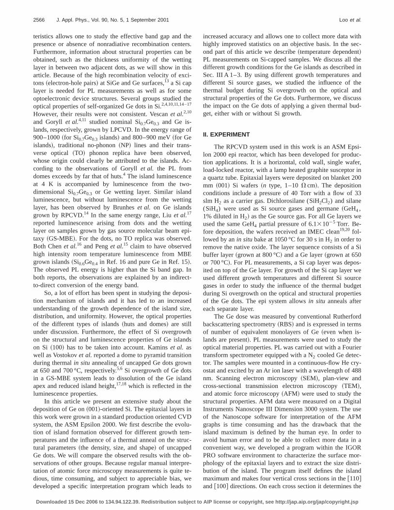
For Ge islands grown and capped at 650 °C, we obsein addition to the Si luminescence only a weak broad babetween 700 and 900 meV, which is probably defect relaApparently, nonradiative recombination centers, like vacarelated complexes, are built into the layers. It is known tthese defects can be passivated by a H2 plasma treatment ate.g., 400 °C.24,27,28After this treatment, SiGe luminescencerecovered~Fig. 13!. The luminescence observed betwe750 meV and 900 meV is an overlap of NP and TO andattributed to islands. The island luminescence has bshifted toward lower energies in comparison to samples wa Ge deposition temperature of 700 °C. Due to lower Si/intermixing, the Ge content in the islands might be highContradictory to the 700 °C case, NP and TO peaks oveeach other, which might be explained by a bigger spreaconfinement energy due to thickness variations. The relavariation in energy quantization increases with decreaslayer thickness. For a deposition temperature of 650 °C,island height is much lower than for a deposition temperatof 700 °C. Furthermore, from the results discussed in SIII A 3, we expect that the spread in island dimensions
Downloaded 15 Dec 2006 to 134.94.122.39. Redistribution subject to AIP
pe
he-n-st
ePL
h
eaeasdf
e
to-t
te
e.e
e-
vedd.yt
senher.p
inegeec.s
retained during Si overgrowth at 650 °C. Plan-view TEconfirms this at least for the lateral dimensions.
The luminescence around 972 and 916 meV is attributo the NP line and the TO replica from the 2D wetting layThe peak energies are lower compared to the sample withsame deposition temperature for the Si cap layer~650 °C! butwith a higher deposition temperature for the Ge lay~700 °C!. This is expected, because the lower growth teperature of the Ge layer leads to higher critical thicknessthe 2D layer before island growth appears. Furthermore,duction of the Ge deposition temperature leads to reduSi/Ge intermixing between the Si buffer layer and thelayer.
Well-resolved island luminescence, with intensities coparable to the best reported values, has been observedcapped islands grown at 700 °C~see Sec. III B1!. Neverthe-less, a treatment in H2 plasma leads to further enhancemeof the island luminescence; see Fig. 14. Both the absoluteintensity as well as the intensity relative to the wetting layand the Si layer are enhanced. This indicates the presendefects or dangling bonds in the as-grown sample, in whXTEM could not detect any extended defects. The influenof a H2 plasma bake on the PL intensity shows the possibifor further improvement of the optical layer properties. Higquality 2D Si/SiGe quantum wells did not show improvment in PL after a H2 plasma bake.24
IV. CONCLUSIONS
In this work, we discussed the growth kinetics observfor Ge island growth in a standard production orientchemical vapor deposition system. Such three-dimensio
FIG. 13. 4 K photoluminescence spectra measured at a laser excitpower of 50 mW/mm2 on Si capped islands for a growth temperature650 °C for both the Ge layer and the Si cap layer. The PL spectra were ton as-grown samples and after a bake in H2 plasma at 400 °C. The bake inH2 plasma passivates defects and enhances island luminescence.
license or copyright, see http://jap.aip.org/jap/copyright.jsp
nd
zeo
he
mi
eanhentthlato
se
..5
nicaraenn
rinb
ntsbylicaesK.
-es-eat-K
hichto-ned,b-
s-
he
ps
th.-
ys.
.
s,
nich
.ith,
E..
r-
ng,
st.
J.
o-
m
50°
2573J. Appl. Phys., Vol. 90, No. 5, 1 September 2001 Loo et al.
Ge islands, imbedded in a matrix with a higher energy bagap, are candidates for new electronic and optoelectronicvices. For device applications control of the island sishape, and uniformity is required. Therefore, the objectivethis work was to obtain improved understanding of tgrowth mechanism during island growth,in situ annealing,and Si overgrowth of the islands.
With increasing deposition time, a changeover fromonomodal to bimodal island distribution appears, whichin agreement with previous studies. The changeover appfor a critical island diameter, which decreases with decreing temperature. Applying a thermal budget after islagrowth initiates lateral Ge surface and Si diffusion from tsubstrate through the islands. This leads to enhancemethe critical diameter and the island height, but does so atexpense island density. Furthermore, depending on the isdistribution after Ge deposition, a transition from hutdome shape or visa versa is observed during thein situ an-neal.
Ge islands can be successfully implemented in Si baoptoelectronic devices, like light emitting diodes~LEDs!29
and Infrared~IR! detectors, and in solar cell applications30
LEDs require light emission in the spectral range of 1.3–1mm and up to room temperature.29 The implementation of Geislands in solar cells should give increased light adsorptiothe IR part.30 We used PL measurements to study the optlayer properties and to obtain information about structulayer properties. A Si cap layer is needed for these PL msurements as well as for the device structures mentioabove. However, nearly total dissolution of small islands atruncation of bigger dome-shaped islands appear dugrowth of the cap layer at 700 °C. This was prevented
FIG. 14. Influence of a treatment in H2 plasma~30 min at 400 °C! on the 20K photoluminescence~measured at a laser excitation power ofmW/mm2!. The growth temperature was 700 °C for the Ge layer and 650for the Si cap layer.
Downloaded 15 Dec 2006 to 134.94.122.39. Redistribution subject to AIP
de-,f
sarss-d
ofe
nd
d
5
inll
a-eddgy
reducing the deposition temperature and by using SiH4 in-stead of SiH2Cl2 as the Si source gas. PL measuremedemonstrate the high layer quality of Si capped islandsthe clear separation between the NP line and the TO repand the high integrated intensities, which was up to 70 timhigher compared to the integrated Si TO intensity at 20Island luminescence appears between 1.35~920 meV! and1.50 mm ~828 meV! which is within the spectral range desired for optoelectronic applications. The high photolumincence intensity could be further enhanced by a thermal trment in a H2 plasma. Clear island luminescence up to 200has been observed after such thermal treatments, wshows the potential of this material system for use in opelectronic device applications. Based on the results obtaiepitaxial layers for LED devices are grown, and device farication is currently ongoing.
ACKNOWLEDGMENTS
The authors wish to thank Bert Brijs and Philippe Rousel for analytical measurements~RBS and TEM, respec-tively! and Patricia Van Marcke for technical assistance. Tauthors are indebted to the European Commission~CEC! forfinancial support in the TMR NetworkAApples No.FMRXCT96-0029. Three of the authors~R.L., P.M.B., andD.D.! are indebted to the CEC for granting them fellowshiin AApples.
1I. N. Stranski and L. Krastanow, Sitzungsber. Akad. Wiss. Wien, MaNaturwiss. Kl., Abt. 2B146, 797 ~1937!.
2L. Vescan, W. Ja¨ger, C. Dieker, K. Schmidt, A. Hartmann, and H. Lu¨th,Mater. Res. Soc. Symp. Proc.263, 23 ~1992!.
3T. I. Kamins, E. C. Carr, R. S. Williams, and S. J. Rosner, J. Appl. Ph81, 211 ~1997!.
4M. Goryll, L. Vescan, and H. Lu¨th, Mater. Sci. Eng., B69–70, 251~2000!.
5N. V. Vostokov, I. V. Dolgov, Yu. N. Drozdov, Z. F. Krasil’nik, D. N.Lobanov, L. D. Moldavskaya, A. V. Novikov, V. V. Postnikov, and D. OFilatov, J. Cryst. Growth209, 302 ~2000!.
6T. I. Kamins, G. Medeiros-Ribeiro, D. A. A. Ohlberg, and R. S. WilliamAppl. Phys. A: Mater. Sci. Process.A67, 727 ~1998!.
7D. E. Jesson, inProperties of Silicon, Germanium and SiGe:Carbo,EMIS Datareviews Ser. No. 24, edited by E. Kasper and K. Lyutov~INSPEC, London, 2000!, Chap. 1.1, pp. 3–8.
8K. Tillmann, H. Trinkaus, and W. Ja¨ger in Ref. 7, Chap. 2.4, pp. 63–749S. A. Chaparro, Y. Zhang, J. Drucker, D. Chandrasekhar, and D. J. SmJ. Appl. Phys.87, 2245~2000!.
10L. Vescan, M. Goryll, T. Stoica, P. Gartner, K. Grimm, O. Chretien,Mateeva, C. Dieker, and B. Holla¨nder, Appl. Phys. A: Mater. Sci. ProcessA71, 423 ~2000!.
11M. Goryll, L. Vescan, and H. Lu¨th, Thin Solid Films336, 244 ~1998!.12M. Goryll, L. Vescan, K. Schmidt, S. Mesters, and H. Lu¨th, Appl. Phys.
Lett. 71, 410 ~1997!.13A. Souifi, G. Bremond, T. Benyattou, G. Guillot, D. Dutartre, and I. Be
bezier, J. Vac. Sci. Technol. B10, 2002~1992!.14T. Brunheset al., Appl. Phys. Lett.77, 1822~2000!.15C. S. Peng, Q. Huang, W. Q. Cheng, J. M. Zhou, Y. H. Zhang, T. T. She
and C. H. Tung, Phys. Rev. B57, 8805~1998!.16H. Chen, W. Q. Cheng, X. G. Xie, Q. Huang, and J. M. Zhou, J. Cry
Growth 171, 61 ~1997!.17J. P. Liu, J. Z. Wang, D. D. Huang, J. P. Li, D. Z. Sun, and M. Y. Kong,
Cryst. Growth207, 150 ~1999!.18P. Sutter and M. G. Lagally, Phys. Rev. Lett.81, 3471~1998!.19M. Meuris, S. Verhaverbeke, P. W. Mertens, H. F. Schmidt, A. L. P. R
tondaro, and M. M. Heyns, Proc-Electrochem. Soc.PV94-7,15 ~1994!.20M. Meuris et al., Proceedings of the 1999 IEEE International Symposiu
C
license or copyright, see http://jap.aip.org/jap/copyright.jsp

D
ms
-
s.
B.
V.
nal
2574 J. Appl. Phys., Vol. 90, No. 5, 1 September 2001 Loo et al.
on Semiconductor Manufacturing, 1999, p. 157.21J. A. Floro, G. A. Lucadamo, E. Chason, L. B. Freund, M. Sinclair, R.
Twesten, and R. Q. Hwang, Phys. Rev. Lett.80, 4717~1998!.22P. Sutter, E. Matteeva, J. S. Sullivan, and M. G. Lagally, Thin Solid Fil
336, 262 ~1998!.23A. Souifi, T. Benyattou, G. Guillot, G. Bre´mond, D. Dutartre, and P. War
ren, J. Appl. Phys.78, 4039~1995!.24R. Loo et al., Thin Solid Films336, 227 ~1998!.25A. Hartmann, C. Dieker, U. Bangert, R. Loo, L. Vescan, and H. Lu¨th,
Appl. Surf. Sci.104Õ105, 502 ~1996!.
Downloaded 15 Dec 2006 to 134.94.122.39. Redistribution subject to AIP
.
26A. St. Amour, J. C. Sturm, Y. Lacroix, and M. L. W. Thewalt, Appl. PhyLett. 65, 3344~1994!.
27I. A. Buyanova, W. M. Chen, A. Henry, W.-X. Ni, G. V. Hansson, andMonemar, Appl. Surf. Sci.102, 293 ~1996!.
28I. A. Buyanova, W. M. Chen, G. Pozina, B. Monemar, W.-X. Ni, and G.Hansson, Appl. Phys. Lett.71, 3676~1997!.
29L. Vescan and T. Stoica, Proc. SPIE3630, 163 ~1999!.30J. Konle, H. Presting, H. Kibbel, K. Thonke, and R. Sauer, Internatio
Conference on Communications, Computers and Devices~ICCCD-2000!,14–16 December 2000, Kharagpur, India~to be published!.
license or copyright, see http://jap.aip.org/jap/copyright.jsp
Related Documents


![PbTe thin films grown by femtosecond pulsed laser deposition. · electrodeposition [5], molecular beam epitaxy [6] and pulsed laser deposition [7,8,9 ] More recently, PbTe grown in](https://static.cupdf.com/doc/110x72/5c0d44a109d3f247038d61bf/pbte-thin-films-grown-by-femtosecond-pulsed-laser-electrodeposition-5-molecular.jpg)


