Strong interaction between graphene edge and metal revealed by scanning tunneling microscopy Hyo Won Kim a , JiYeon Ku a , Wonhee Ko a , Insu Jeon a , Hyeokshin Kwon a , Seunghwa Ryu b , Se-Jong Kahng a,c , Sung-Hoon Lee a , Sung Woo Hwang a , Hwansoo Suh a, * a Samsung Advanced Institute of Technology, Suwon 443-803, Republic of Korea b Department of Mechanical Engineering, Korea Advanced Institute of Science and Technology (KAIST), Daejeon 305-701, Republic of Korea c Department of Physics, Korea University, 1-5 Anam-dong, Seongbuk-gu, Seoul 136-713, Republic of Korea ARTICLE INFO Article history: Received 16 April 2014 Accepted 28 June 2014 Available online 5 July 2014 ABSTRACT The interaction between a graphene edge and the underlying metal is investigated through the use of scanning tunneling microscopy (STM) and density functional theory (DFT) calculations and found to influence the geometrical structure of the graphene edge and its electronic properties. STM study reveals that graphene nanoislands grow on a Pt(1 1 1) surface with the considerable bending of the graphene at the edge arising from the strong graphene-edge–Pt-substrate interactions. Periodic ripples along the graphene edge due to both the strong interaction and the lattice mismatch with the underlying metal were seen. DFT calculations confirm such significant bending and also reproduce the periodic ripples along the graphene edge. The highly distorted edge geometry causes strain-induced pseudo-magnetic fields, which are manifested as Landau levels in the scanning tunneling spectroscopy. The electronic properties of the graphene edge are thus concluded to be strongly influenced by the curvature rather than the localized states along the zigzag edge as was previously predicted. Ó 2014 Elsevier Ltd. All rights reserved. 1. Introduction Graphene is a promising building block for future electronic devices [1,2] but actualizing this enormous promise and real- izing graphene-based devices requires a thorough under- standing of how the contact between graphene and the underlying metal substrate affects the electronic properties of graphene. Metallic contacts to graphene are known to influence doping [3–5] and can result in the opening of a band gap [6–8], which in turn significantly modifies the transport properties. The electronic properties of graphene on metal substrates also strongly depend on the nature of the graph- ene–metal interaction. Graphene grown by chemical vapor deposition on various metal surfaces has enabled such prop- erties at graphene–metal interfaces to be investigated [8–10], and the influence of different substrates has been studied for metal surfaces such as Ni(1 1 1) [7,11], Co(0 0 0 1) [12], Rh(1 1 1) [13,14], Ru(0001) [6], Ir(111) [15], Pt(111) [16], and Cu(1 1 1) [17,18]. The strength of inter-material interactions will also affect the electronic properties of graphene; for http://dx.doi.org/10.1016/j.carbon.2014.06.071 0008-6223/Ó 2014 Elsevier Ltd. All rights reserved. * Corresponding author. E-mail address: [email protected] (H. Suh). CARBON 78 (2014) 190 – 195 Available at www.sciencedirect.com ScienceDirect journal homepage: www.elsevier.com/locate/carbon

Welcome message from author
This document is posted to help you gain knowledge. Please leave a comment to let me know what you think about it! Share it to your friends and learn new things together.
Transcript
C A R B O N 7 8 ( 2 0 1 4 ) 1 9 0 – 1 9 5
.sc iencedi rect .com
Avai lab le at wwwScienceDirect
journal homepage: www.elsev ier .com/ locate /carbon
Strong interaction between graphene edgeand metal revealed by scanning tunnelingmicroscopy
http://dx.doi.org/10.1016/j.carbon.2014.06.0710008-6223/� 2014 Elsevier Ltd. All rights reserved.
* Corresponding author.E-mail address: [email protected] (H. Suh).
Hyo Won Kim a, JiYeon Ku a, Wonhee Ko a, Insu Jeon a, Hyeokshin Kwon a,Seunghwa Ryu b, Se-Jong Kahng a,c, Sung-Hoon Lee a, Sung Woo Hwang a,Hwansoo Suh a,*
a Samsung Advanced Institute of Technology, Suwon 443-803, Republic of Koreab Department of Mechanical Engineering, Korea Advanced Institute of Science and Technology (KAIST), Daejeon 305-701, Republic of Koreac Department of Physics, Korea University, 1-5 Anam-dong, Seongbuk-gu, Seoul 136-713, Republic of Korea
A R T I C L E I N F O A B S T R A C T
Article history:
Received 16 April 2014
Accepted 28 June 2014
Available online 5 July 2014
The interaction between a graphene edge and the underlying metal is investigated through
the use of scanning tunneling microscopy (STM) and density functional theory (DFT)
calculations and found to influence the geometrical structure of the graphene edge and
its electronic properties. STM study reveals that graphene nanoislands grow on a Pt(111)
surface with the considerable bending of the graphene at the edge arising from the strong
graphene-edge–Pt-substrate interactions. Periodic ripples along the graphene edge due to
both the strong interaction and the lattice mismatch with the underlying metal were seen.
DFT calculations confirm such significant bending and also reproduce the periodic ripples
along the graphene edge. The highly distorted edge geometry causes strain-induced
pseudo-magnetic fields, which are manifested as Landau levels in the scanning tunneling
spectroscopy. The electronic properties of the graphene edge are thus concluded to be
strongly influenced by the curvature rather than the localized states along the zigzag edge
as was previously predicted.
� 2014 Elsevier Ltd. All rights reserved.
1. Introduction
Graphene is a promising building block for future electronic
devices [1,2] but actualizing this enormous promise and real-
izing graphene-based devices requires a thorough under-
standing of how the contact between graphene and the
underlying metal substrate affects the electronic properties
of graphene. Metallic contacts to graphene are known to
influence doping [3–5] and can result in the opening of a band
gap [6–8], which in turn significantly modifies the transport
properties. The electronic properties of graphene on metal
substrates also strongly depend on the nature of the graph-
ene–metal interaction. Graphene grown by chemical vapor
deposition on various metal surfaces has enabled such prop-
erties at graphene–metal interfaces to be investigated [8–10],
and the influence of different substrates has been studied
for metal surfaces such as Ni(111) [7,11], Co(0001) [12],
Rh(111) [13,14], Ru(0001) [6], Ir(111) [15], Pt(111) [16], and
Cu(111) [17,18]. The strength of inter-material interactions
will also affect the electronic properties of graphene; for
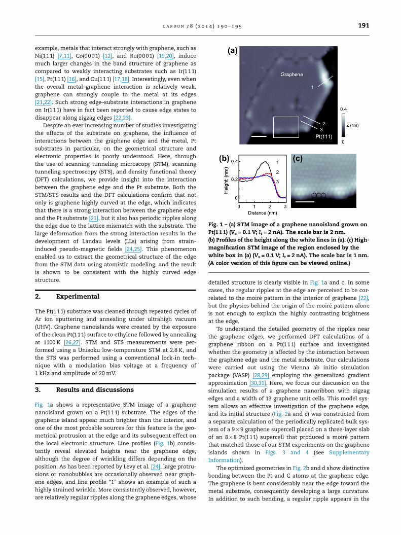
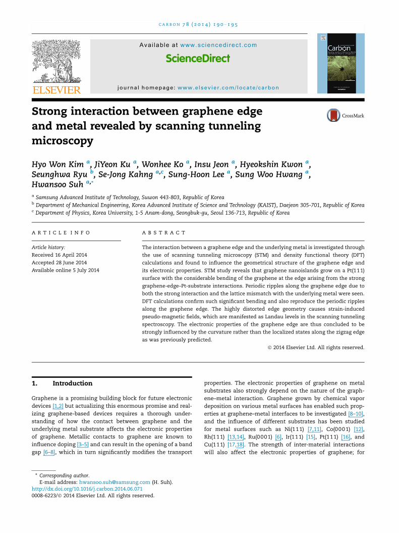
Fig. 1 – (a) STM image of a graphene nanoisland grown on
Pt(111) (Vs = 0.1 V; It = 2 nA). The scale bar is 2 nm.
(b) Profiles of the height along the white lines in (a). (c) High-
magnification STM image of the region enclosed by the
white box in (a) (Vs = 0.1 V; It = 2 nA). The scale bar is 1 nm.
(A color version of this figure can be viewed online.)
C A R B O N 7 8 ( 2 0 1 4 ) 1 9 0 – 1 9 5 191
example, metals that interact strongly with graphene, such as
Ni(111) [7,11], Co(0001) [12], and Ru(0001) [19,20], induce
much larger changes in the band structure of graphene as
compared to weakly interacting substrates such as Ir(111)
[15], Pt(111) [16], and Cu(111) [17,18]. Interestingly, even when
the overall metal–graphene interaction is relatively weak,
graphene can strongly couple to the metal at its edges
[21,22]. Such strong edge–substrate interactions in graphene
on Ir(111) have in fact been reported to cause edge states to
disappear along zigzag edges [22,23].
Despite an ever increasing number of studies investigating
the effects of the substrate on graphene, the influence of
interactions between the graphene edge and the metal, Pt
substrates in particular, on the geometrical structure and
electronic properties is poorly understood. Here, through
the use of scanning tunneling microscopy (STM), scanning
tunneling spectroscopy (STS), and density functional theory
(DFT) calculations, we provide insight into the interaction
between the graphene edge and the Pt substrate. Both the
STM/STS results and the DFT calculations confirm that not
only is graphene highly curved at the edge, which indicates
that there is a strong interaction between the graphene edge
and the Pt substrate [21], but it also has periodic ripples along
the edge due to the lattice mismatch with the substrate. The
large deformation from the strong interaction results in the
development of Landau levels (LLs) arising from strain-
induced pseudo-magnetic fields [24,25]. This phenomenon
enabled us to extract the geometrical structure of the edge
from the STM data using atomistic modeling, and the result
is shown to be consistent with the highly curved edge
structure.
2. Experimental
The Pt(111) substrate was cleaned through repeated cycles of
Ar ion sputtering and annealing under ultrahigh vacuum
(UHV). Graphene nanoislands were created by the exposure
of the clean Pt(111) surface to ethylene followed by annealing
at 1100 K [26,27]. STM and STS measurements were per-
formed using a Unisoku low-temperature STM at 2.8 K, and
the STS was performed using a conventional lock-in tech-
nique with a modulation bias voltage at a frequency of
1 kHz and amplitude of 20 mV.
3. Results and discussions
Fig. 1a shows a representative STM image of a graphene
nanoisland grown on a Pt(111) substrate. The edges of the
graphene island appear much brighter than the interior, and
one of the most probable sources for this feature is the geo-
metrical protrusion at the edge and its subsequent effect on
the local electronic structure. Line profiles (Fig. 1b) consis-
tently reveal elevated heights near the graphene edge,
although the degree of wrinkling differs depending on the
position. As has been reported by Levy et al. [24], large protru-
sions or nanobubbles are occasionally observed near graph-
ene edges, and line profile ‘‘1’’ shows an example of such a
highly strained wrinkle. More consistently observed, however,
are relatively regular ripples along the graphene edges, whose
detailed structure is clearly visible in Fig. 1a and c. In some
cases, the regular ripples at the edge are perceived to be cor-
related to the moire pattern in the interior of graphene [22],
but the physics behind the origin of the moire pattern alone
is not enough to explain the highly contrasting brightness
at the edge.
To understand the detailed geometry of the ripples near
the graphene edges, we performed DFT calculations of a
graphene ribbon on a Pt(111) surface and investigated
whether the geometry is affected by the interaction between
the graphene edge and the metal substrate. Our calculations
were carried out using the Vienna ab initio simulation
package (VASP) [28,29] employing the generalized gradient
approximation [30,31]. Here, we focus our discussion on the
simulation results of a graphene nanoribbon with zigzag
edges and a width of 13 graphene unit cells. This model sys-
tem allows an effective investigation of the graphene edge,
and its initial structure (Fig. 2a and c) was constructed from
a separate calculation of the periodically replicated bulk sys-
tem of a 9 · 9 graphene supercell placed on a three-layer slab
of an 8 · 8 Pt(111) supercell that produced a moire pattern
that matched those of our STM experiments on the graphene
islands shown in Figs. 3 and 4 (see Supplementary
Information).
The optimized geometries in Fig. 2b and d show distinctive
bonding between the Pt and C atoms at the graphene edge.
The graphene is bent considerably near the edge toward the
metal substrate, consequently developing a large curvature.
In addition to such bending, a regular ripple appears in the
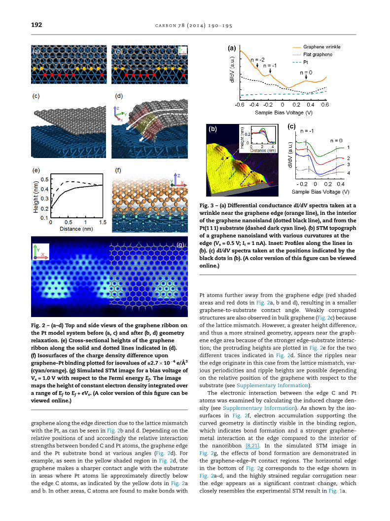
Fig. 2 – (a–d) Top and side views of the graphene ribbon on
the Pt model system before (a, c) and after (b, d) geometry
relaxation. (e) Cross-sectional heights of the graphene
ribbon along the solid and dotted lines indicated in (d).
(f) Isosurfaces of the charge density difference upon
graphene–Pt binding plotted for isovalues of ±2.7 · 10�4 e/A3
(cyan/orange). (g) Simulated STM image for a bias voltage of
Vs = 1.0 V with respect to the Fermi energy Ef. The image
maps the height of constant electron density integrated over
a range of Ef to Ef + eVs. (A color version of this figure can be
viewed online.)
Fig. 3 – (a) Differential conductance dI/dV spectra taken at a
wrinkle near the graphene edge (orange line), in the interior
of the graphene nanoisland (dotted black line), and from the
Pt(111) substrate (dashed dark cyan line). (b) STM topograph
of a graphene nanoisland with various curvatures at the
edge (Vs = 0.5 V; It = 1 nA). Inset: Profiles along the lines in
(b). (c) dI/dV spectra taken at the positions indicated by the
black dots in (b). (A color version of this figure can be viewed
online.)
192 C A R B O N 7 8 ( 2 0 1 4 ) 1 9 0 – 1 9 5
graphene along the edge direction due to the lattice mismatch
with the Pt, as can be seen in Fig. 2b and d. Depending on the
relative positions of and accordingly the relative interaction
strengths between bonded C and Pt atoms, the graphene edge
and the Pt substrate bond at various angles (Fig. 2d). For
example, as seen in the yellow shaded region in Fig. 2d, the
graphene makes a sharper contact angle with the substrate
in areas where Pt atoms lie approximately directly below
the edge C atoms, as indicated by the yellow dots in Fig. 2a
and b. In other areas, C atoms are found to make bonds with
Pt atoms further away from the graphene edge (red shaded
areas and red dots in Fig. 2a, b and d), resulting in a smaller
graphene-to-substrate contact angle. Weakly corrugated
structures are also observed in bulk graphene (Fig. 2c) because
of the lattice mismatch. However, a greater height difference,
and thus a more strained geometry, appears near the graph-
ene edge area because of the stronger edge–substrate interac-
tion; the protruding heights are plotted in Fig. 2e for the two
different traces indicated in Fig. 2d. Since the ripples near
the edge originate in this case from the lattice mismatch, var-
ious periodicities and ripple heights are possible depending
on the relative position of the graphene with respect to the
substrate (see Supplementary Information).
The electronic interaction between the edge C and Pt
atoms was examined by calculating the induced charge den-
sity (see Supplementary Information). As shown by the iso-
surfaces in Fig. 2f, electron accumulation supporting the
curved geometry is distinctly visible in the binding region,
which indicates bond formation and a stronger graphene–
metal interaction at the edge compared to the interior of
the nanoribbon [8,21]. In the simulated STM image in
Fig. 2g, the effects of bond formation are demonstrated in
the graphene-edge–Pt contact regions. The horizontal edge
in the bottom of Fig. 2g corresponds to the edge shown in
Fig. 2a–d, and the highly strained regular corrugation near
the edge appears as a significant contrast change, which
closely resembles the experimental STM result in Fig. 1a.
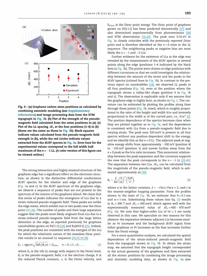
Fig. 4 – (a) Graphene carbon atom positions as calculated by
combining atomistic modeling (see Supplementary
Information) and image processing data from the STM
topograph in Fig. 3b. (b) Plot of the strength of the pseudo-
magnetic field calculated from the atom positions in (a). (c)
Plot of the LL spacing DE1 at the four positions (1–4) in (b)
(these are the same as those in Fig. 3b). Black squares
indicate values calculated from the pseudo-magnetic field
strength in (b), while the red circles indicate values
extracted from the dI/dV spectra in Fig. 3c. Error bars for the
experimental values correspond to the full width half
maximum of the n = �1 LL. (A color version of this figure can
be viewed online.)
C A R B O N 7 8 ( 2 0 1 4 ) 1 9 0 – 1 9 5 193
The strong interaction and highly strained structure of the
graphene edge has a significant effect on the electronic struc-
ture, as shown in the distinctive differential conductance
dI/dV spectra for the interior and edge of the graphene
(Fig. 3a and c). In the dI/dV spectrum of the graphene edge,
we observe a sequence of peaks that are not present in the
spectrum of the interior of the graphene island. We claim that
this series of peaks indicates the emergence of LLs due to a
strain-induced pseudo-magnetic field. These peaks are unlike
the edge states, which exhibit one or two peaks near the Dirac
point [32–34]. The number of peaks and their large separation
suggest that the peaks most likely originate from LLs due to a
strain-induced pseudo-magnetic field from the large lattice
distortion at the edge, as reported previously for graphene
nanobubbles grown on Pt(111) [24] and Ru(0001) [25]. Indeed,
the peak positions are consistent with the energies of the LLs
for which the relativistic nature of the massless Dirac parti-
cles results in an unusual LL sequence [24,25,35,36]
En ¼ sgnðnÞffiffiffiffiffiffiffiffiffiffiffiffiffiffiffiffiffiffiffiffiffiffi2e�hm2
FBsjnjq
þ EDirac; n ¼ 0;�1;�2; . . . ; ð1Þ
where En is the nth LL energy with respect to the Fermi level,
Bs is the pseudo-magnetic field, e is the electron charge, �h is
the reduced Planck constant, mF is the Fermi velocity, and
EDirac is the Dirac point energy. The Dirac point of graphene
grown on Pt(111) has been predicted theoretically [37] and
also determined experimentally from photoemission [38]
and STM observations [16,24]. The peak near 0.32 eV in
Fig. 3a closely coincides with the previously reported Dirac
point and is therefore identified as the n = 0 state in the LL
sequence. The neighboring peaks at negative bias are most
likely the n = �1 and �2 LLs.
Further evidence for the existence of LLs at the edge was
revealed by the measurement of the dI/dV spectra at several
points along the edge (positions 1–4 indicated by the black
dots in Fig. 3b). The points were chosen at edge positions with
different curvatures so that we could investigate the relation-
ship between the amount of the strain and the peaks in the
dI/dV spectra (colored lines in Fig. 3b). In contrast to the pre-
vious report on nanobubbles [24], we observed LL peaks at
all four positions (Fig. 3c), even at the position where the
topograph shows a valley-like shape (position 4 in Fig. 3b
and c). The observation is explicable only if we assume that
the graphene edge is highly bent, as shown in Fig. 2. The cur-
vature can be estimated by plotting the profiles along lines
through these points (Fig. 3b, inset), which is roughly propor-
tional to the ratio of the height and width h/w and inversely
proportional to the width w of the curved part, i.e., h/w2 [2].
The position dependence of the spectra becomes clear when
they are plotted together as in Fig. 3c, and the dependence
is consistent with LLs from a pseudo-magnetic field due to
varying strain. The peak near 320 meV is present in all four
spectra without any position-dependent shift in the energy,
and we identify this as the n = 0 LL. The adjacent peak at neg-
ative energy shifts from approximately �100 mV (position 4)
to �150 mV (position 1) and moves further away from the
n = 0 peak as the h/w ratio increases. This monotonic relation-
ship between the peak separation and the curvature supports
the view that the peak corresponds to the n = �1 LL [39,40].
The separation between two LLs, DE1, can be calculated from
the magnitude of the pseudo-magnetic field, which is esti-
mated approximately as [39]
Bs �b
awhw
� �2 2p�he
� �; ð2Þ
where a is the lattice constant, b ¼ �@ ln t=@ ln a � 2, and t is
the nearest-neighbor hopping parameter. From the profiles
shown in the inset of Fig. 3b, we estimate that h = 0.1 nm
and w = 1 nm. Substituting these values into Eq. (2) results
in Bs � 300 T and DE1 � 500 meV, which agrees well with the
experimentally measured value of DE1 = 400 � 470 meV
(Fig. 3c). We note that higher-order LLs of |n| P 2 are rarely
observed in this case. We speculate on two reasons for this
absence: the separation between adjacent LLs becomes smal-
ler as |n| increases and the background dI/dV signal from
either graphene or Pt increases as the bias increases further
from the Fermi energy.
For a more quantitative analysis, we calculated the spatial
dependence of the strain-induced pseudo-magnetic field
from the topograph shown in Fig. 3b. To obtain the strain
map, we assumed that the topograph height corresponded
to the actual geometry of the graphene and then extracted
all the atomic positions by combining the image processing
and atomistic modeling data, as shown in Fig. 4a (see
194 C A R B O N 7 8 ( 2 0 1 4 ) 1 9 0 – 1 9 5
Supplementary Information). The pseudo-magnetic field Bs is
calculated as [40]
Bs ¼ r�A; A ¼ ba
uxx � uyy
�2uxy
� �; ð3Þ
where A is the vector potential, and uij is the two-dimensional
strain field. The resulting pseudo-magnetic field is plotted in
Fig. 4b. Regions with high pseudo-magnetic field are concen-
trated along the graphene edge with the highest fields on the
most protruded parts. The magnitude of the field is in the
range of 200–500 T, which is consistent with the rough esti-
mate from Eq. (2). Because of the ripples along the edge, the
field across the edge shows the variations that can be directly
compared with the DE1 values extracted from the dI/dV spec-
tra in Fig. 3c. These DE1 values from the experiment at posi-
tions 1–4 in Fig. 3b are plotted as the red circles in Fig. 4c
and those from the calculated pseudo-magnetic field at the
same positions are plotted as black squares (except for
the value at position 2, which was too close to the edge for
the pseudo-magnetic field to be calculated). We find that
there is good agreement, and both the experiment and simu-
lation results show the same tendency: an edge with a lower
curvature has a lower DE1 value. A discrepancy of about
200 meV is tolerable considering the uncertainty in the value
of b and possible errors in the atomistic modeling of the
atomic positions. The analysis results of the pseudo-magnetic
field support the existence of large strain at the edge, which is
manifested as the highly bent, rippled graphene edge.
4. Conclusion
In this study, we have demonstrated the interaction between
a graphene edge and the underlying metal substrate, and this
interaction has been shown to influence the geometrical
structure of the graphene edge and its electronic properties.
Graphene on a Pt (111) surface was found to bend signifi-
cantly at the edges due to these strong interactions with the
metal substrate and to form periodic ripples along the edge
due to the lattice mismatch. Our STS measurements revealed
the development of LLs as a result of pseudo-magnetic fields
induced by the bent geometry. Therefore, our results suggest
that the electronic properties of graphene near its edges are
more strongly affected by the curvature in the graphene than
by the localized zigzag edge states. These results also provide
an important understanding of how the contact between a
graphene edge and a metal surface shape the geometrical
and electronic properties.
Funding Sources
S. Ryu acknowledges the support of the Basic Science
Research Program through the National Research Foundation
of Korea (NRF) funded by the Ministry of Science, ICT & Future
Planning (2013010091).
Acknowledgment
We thank Young-Woo Son at the Korea Institute for Advanced
Study and Youngtek Oh at the Samsung Advanced Institute of
Technology for helpful discussions.
Appendix A. Supplementary data
Supplementary data associated with this article can be found,
in the online version, at http://dx.doi.org/10.1016/j.carbon.
2014.06.071.
R E F E R E N C E S
[1] Geim AK, Novoselov KS. The rise of graphene. Nat Mater2007;6:183–91.
[2] Castro Neto AH, Guinea F, Peres NMR, Novoselov KS, GeimAK. The electronic properties of graphene. Rev Mod Phys2009;81(1):109–62.
[3] Lee EJH, Balasubramanian K, Weitz RT, Burghard M, Kern K.Contact and edge effects in graphene devices. NatNanotechnol 2008;3(8):486–90.
[4] Khomyakov PA, Giovannetti G, Rusu PC, Brocks G, van denBrink J, Kelly PJ. First-principles study of the interaction andcharge transfer between graphene and metals. Phys Rev B2009;79(19):195425.
[5] Khomyakov PA, Starikov AA, Brocks G, Kelly PJ. Nonlinearscreening of charges induced in graphene by metal contacts.Phys Rev B 2010;82(11):115437.
[6] Enderlein C, Kim YS, Bostwick A, Rotenberg E, Horn K. Theformation of an energy gap in graphene on ruthenium bycontrolling the interface. New J Phys 2010;12(3):033014.
[7] Varykhalov A, Scholz MR, Kim TK, Rader O. Effect of noble-metal contacts on doping and band gap of graphene. PhysRev B 2010;82(12):121101.
[8] Voloshina E, Dedkov Y. Graphene on metallic surfaces:problems and perspectives. Phys Chem Chem Phys2012;14(39):13502–14.
[9] Wintterlin J, Bocquet ML. Graphene on metal surfaces. SurfSci 2009;603(10–12):1841–52.
[10] Batzill M. The surface science of graphene: metal interfaces,CVD synthesis, nanoribbons, chemical modifications, anddefects. Surf Sci Rep 2012;67(3–4):83–115.
[11] Nagashima A, Tejima N, Oshima C. Electronic states of thepristine and alkali-metal-intercalated monolayer graphite/Ni(111) systems. Phys Rev B 1994;50(23):17487–95.
[12] Eom D, Prezzi D, Rim KT, Zhou H, Lefenfeld M, Xiao S, et al.Structure and electronic properties of graphene nanoislandson Co(0001). Nano Lett 2009;9(8):2844–8.
[13] Wang B, Caffio M, Bromley C, Fruchtl H, Schaub R. Couplingepitaxy, chemical bonding, and work function at the localscale in transition metal-supported graphene. ACS Nano2010;4(10):5773–82.
[14] Voloshina EN, Dedkov YS, Torbrugge S, Thissen A, Fonin M.Graphene on Rh(111): scanning tunneling and atomic forcemicroscopies studies. Appl Phys Lett 2012;100(24):241606.
[15] Busse C et al. Graphene on Ir(111): physisorption withchemical modulation. Phys Rev Lett 2011;107(3):036101.
[16] Ugeda MM, Fernandez-Torre D, Brihuega I, Pou P, Martınez-Galera AJ, Perez R, et al. Point defects on graphene on metals.Phys Rev Lett 2011;107(11):116803.
[17] Gao L, Guest JR, Guisinger NP. Epitaxial graphene on Cu(111).Nano Lett 2010;10(9):3512–6.
[18] Jeon I, Yang H, Lee S-H, Heo J, Seo DH, Shin J, et al.Passivation of metal surface states: microscopic origin foruniform monolayer graphene by low temperature chemicalvapor deposition. ACS Nano 2011;5(3):1915–20.
[19] Marchini S, Gunther S, Wintterlin J. Scanning tunnelingmicroscopy of graphene on Ru(0001). Phys Rev B2007;76(7):075429.
[20] Sutter PW, Flege J-I, Sutter EA. Epitaxial graphene onruthenium. Nat Mater 2008;7(5):406–11.
C A R B O N 7 8 ( 2 0 1 4 ) 1 9 0 – 1 9 5 195
[21] Lacovig P, Pozzo M, Alfe D, Vilmercati P, Baraldi A, Lizzit S.Growth of dome-shaped carbon nanoislands on Ir(111): theintermediate between carbidic clusters and quasi-free-standing graphene. Phys Rev Lett 2009;103(16):166101.
[22] S-h Phark, Borme J, Vanegas AL, Corbetta M, Sander D,Kirschner J. Atomic structure and spectroscopy of grapheneedges on Ir(111). Phys Rev B 2012;86(4):045442.
[23] Li Y et al. Absence of edge states in covalently bonded zigzagedges of graphene on Ir(111). Adv Mater 2013;25(14):1967–72.
[24] Levy N, Burke SA, Meaker KL, Panlasigui M, Zettl A, Guinea F,et al. Strain-induced pseudo-magnetic fields greater than300 tesla in graphene nanobubbles. Science2010;329(5991):544–7.
[25] Lu J, Neto AHC, Loh KP. Transforming moire blisters intogeometric graphene nano-bubbles. Nat Commun 2012;3:823.
[26] Land TA, Michely T, Behm RJ, Hemminger JC, Comsa G. STMinvestigation of single layer graphite structures produced onPt(111) by hydrocarbon decomposition. Surf Sci1992;264(3):261–70.
[27] Enachescu M, Schleef D, Ogletree DF, Salmeron M. Integrationof point-contact microscopy and atomic-force microscopy:application to characterization of graphite/Pt(111). Phys RevB 1999;60(24):16913–9.
[28] Kresse G, Furthmuller J. Efficiency of ab-initio total energycalculations for metals and semiconductors using a plane-wave basis set. Comp Mater Sci 1996;6(1):15–50.
[29] Kresse G, Furthmuller J. Efficient iterative schemes forab initio total-energy calculations using a plane-wave basisset. Phys Rev B 1996;54(16):11169–86.
[30] Perdew JP, Burke K, Ernzerhof M. Generalized gradientapproximation made simple. Phys Rev Lett1996;77(18):3865–8.
[31] Perdew JP, Burke K, Ernzerhof M. Generalized gradientapproximation made simple. Phys Rev Lett 1997;78(7):1396.
[32] Tao C et al. Spatially resolving edge states of chiral graphenenanoribbons. Nat Phys 2011;7(8):616–20.
[33] Kobayashi Y, Fukui K-i, Enoki T, Kusakabe K, Kaburagi Y.Observation of zigzag and armchair edges of graphite usingscanning tunneling microscopy and spectroscopy. Phys Rev B2005;71(19):193406.
[34] Pan M, Girao EC, Jia X, Bhaviripudi S, Li Q, Kong J, et al.Topographic and spectroscopic characterization of electronicedge states in CVD grown graphene nanoribbons. Nano Lett2012;12(4):1928–33.
[35] Li G, Andrei EY. Observation of Landau levels of Diracfermions in graphite. Nat Phys 2007;3(9):623–7.
[36] Gomes KK, Mar W, Ko W, Guinea F, Manoharan HC. DesignerDirac fermions and topological phases in moleculargraphene. Nature 2012;483(7389):306–10.
[37] Giovannetti G, Khomyakov PA, Brocks G, Karpan VM, van denBrink J, Kelly PJ. Doping graphene with metal contacts. PhysRev Lett 2008;101(2):026803.
[38] Sutter P, Sadowski JT, Sutter E. Graphene on Pt(111): growthand substrate interaction. Phys Rev B 2009;80(24):245411.
[39] Guinea F, Katsnelson MI, Vozmediano MAH. Midgap statesand charge inhomogeneities in corrugated graphene. PhysRev B 2008;77(20):075422.
[40] Guinea F, Katsnelson MI, Geim AK. Energy gaps and a zero-field quantum hall effect in graphene by strain engineering.Nat Phys 2010;6(1):30–3.
Related Documents