COMMUNICATION © 2015 WILEY-VCH Verlag GmbH & Co. KGaA, Weinheim (1 of 7) 1400038 wileyonlinelibrary.com Stretchable and Conformable Oxide Thin-Film Electronics Niko Münzenrieder,* Giuseppe Cantarella, Christian Vogt, Luisa Petti, Lars Büthe, Giovanni A. Salvatore, Yang Fang, Renzo Andri, Yawhuei Lam, Rafael Libanori, Daniel Widner, André R. Studart, and Gerhard Tröster Dr. N. Münzenrieder Sensor Technology Research Center School of Engineering and Informatics University of Sussex BN1 9QT Falmer, Brighton, UK E-mail: [email protected] Dr. N. Münzenrieder, G. Cantarella, C. Vogt, L. Petti, L. Büthe, Dr. G. A. Salvatore, Y. Fang, R. Andri, Y. Lam, Prof. G. Tröster Electronics Laboratory Department of Information Technology and Electrical Engineering ETH Zurich, Gloriastrasse 35, 8092 Zürich, Switzerland Dr. R. Libanori, D. Widner, Prof. A. R. Studart Complex Materials Department of Materials ETH Zurich, Wolfgang-Pauli-Str. 10, 8093 Zürich, Switzerland DOI: 10.1002/aelm.201400038 gains its elasticity from its accordion-like structure. Such struc- tures are generally realized using prestrained substrates, where the relaxation of the substrate after the fabrication leads to the formation of wrinkles on the surface. Wavy transistors made of organic materials or silicon nanomembranes demonstrated stretchability >200%. [6,21,24] This method also enabled stretch- able magnetic field sensors, [25] and organic light-emitting diodes. [26] Even more challenging than the fabrication of stretchable electronics devices is the realization of conformal electronics which is stretchable in multiple dimensions. [12] 3D deformed a-Si TFTs on a spherical dome can survive strains of 6%, [27] and wavy organic electronic components on a biaxial prestretched elastomer are able to withstand a 35% area decrease. [6] The challenges concerning the fabrication of stretchable active electronic devices can be summarized as follows: Stretch- able substrates need to provide thermal, mechanical, and chemical stability, as well as a surface roughness compatible with the device fabrication process. [28] Additionally, wavy elec- tronics need to survive extremely small bending radii, in the micrometer range, caused by the wrinkles, elastomers with stiff islands at the same time have to overcome the delamina- tion problem caused by stress localization at the interfaces. Here, two approaches based on wavy electronics, as well as on locally reinforced composite substrates are investigated. Both techniques result in inorganic electronic devices reversibly stretchable to strain values >200%. Furthermore, the developed technology is used to demonstrate the basic components of a stretchable electronic system, including a sensor and integrated circuits for signal processing and power transmission wrapped around 3D surfaces. This proves the potential of the presented technology for electronic skins and smart implants. The fabrication of electronic devices in general requires temperatures above 100 °C, the use of different etchants and solvents, as well as a substrate surface roughness in the nano- meter range. Since these requirements are hardly compatible with elastic substrates, [28] the proposed stretchable electronics is manufactured in a two-step process: The devices are fabri- cated on a rigid substrate and afterwards transferred to an elas- tomeric polymer. A silicon wafer covered with polyvinyl alcohol (PVA) and parylene is used as substrate. After the device fab- rication is finished, the PVA is dissolved in water and the 1 μm-thin parylene membrane carrying the electronic devices is released (Figure S1, Supporting Information), [8] and transferred to any arbitrary new substrate. Since transistors are the most important building blocks for all electronic systems, Figure 1a shows a schematic of the fabricated thin-film transistors based on amorphous indium-gallium-zinc-oxide (IGZO) as semicon- ductor, high-k Aluminum oxide ( ε r ≈ 9.5) as gate insulator and Nowadays, electronics is diverging from being bulky and rigid and is becoming lightweight and flexible. This development not only leads to new applications covering all aspects of wear- able electronics, [1] ranging from smart textiles [2] to skin mount devices, [3] but enables also new cost efficient fabrication tech- niques. [4] Extremely bendable electronics based on amorphous silicon, [5] organic, [6,7] and oxide [8] semiconductors have been realized by the use of micrometer thin substrates. However, epidermal electronics, [9,10] smart implants, [11] or artificial elec- tronic skins for robots [12] require stretchable electronic devices. Since the stretchability of human skin varies between 20% and 70%, [9,13] elastic electronics have to survive similar elongations. State-of-the-art elastic electronics are classified into three main groups: first, conductive interconnection lines can be realized by using intrinsically elastic conductors, [14] air-bridge structures, [15] and metal lines on prestretched substrates [16] or patterned into meander-like geometries. [17] Examples are carbon nanotubes embedded into a rubber matrix (stretchable up to 100%), [14] or metal films on porous polydimethylsiloxane (PDMS) (stretchable by 80%). [18] Furthermore, oxide transistors roll-transferred to elastic PDMS substrates can be stretched by 5%. [19] Significantly more stretchable active devices made from brittle materials are realized by two other approaches, namely by the fabrication on elastomeric substrates with stiff islands and by the use of “wavy” layouts using prestretched substrates. [20,21] The use of stiff islands allows minimizing the strain experienced by the devices. Here 20% stretchability was achieved for amorphous silicon and oxide thin-film transistors (TFTs) fabricated on PDMS patterned with stiff polyimide or epoxy-based photoresist islands. [22] At the same time off-the- shelf LEDs on an elastic composite substrate stayed functional while strained by 150%. [23] On the other hand, wavy electronics www.MaterialsViews.com www.advelectronicmat.de Adv. Electron. Mater. 2015, 1, 1400038

Welcome message from author
This document is posted to help you gain knowledge. Please leave a comment to let me know what you think about it! Share it to your friends and learn new things together.
Transcript
CO
MM
UN
ICATIO
N
© 2015 WILEY-VCH Verlag GmbH & Co. KGaA, Weinheim (1 of 7) 1400038wileyonlinelibrary.com
Stretchable and Conformable Oxide Thin-Film Electronics
Niko Münzenrieder ,* Giuseppe Cantarella , Christian Vogt , Luisa Petti , Lars Büthe , Giovanni A. Salvatore , Yang Fang , Renzo Andri , Yawhuei Lam , Rafael Libanori , Daniel Widner , André R. Studart , and Gerhard Tröster
Dr. N. Münzenrieder Sensor Technology Research Center School of Engineering and Informatics University of Sussex BN1 9QT Falmer , Brighton , UK E-mail: [email protected] Dr. N. Münzenrieder, G. Cantarella, C. Vogt, L. Petti, L. Büthe, Dr. G. A. Salvatore, Y. Fang, R. Andri, Y. Lam, Prof. G. Tröster Electronics Laboratory Department of Information Technology and Electrical Engineering ETH Zurich, Gloriastrasse 35, 8092 Zürich , Switzerland Dr. R. Libanori, D. Widner, Prof. A. R. Studart Complex Materials Department of MaterialsETH Zurich, Wolfgang-Pauli-Str. 10, 8093 Zürich , Switzerland
DOI: 10.1002/aelm.201400038
gains its elasticity from its accordion-like structure. Such struc-tures are generally realized using prestrained substrates, where the relaxation of the substrate after the fabrication leads to the formation of wrinkles on the surface. Wavy transistors made of organic materials or silicon nanomembranes demonstrated stretchability >200%. [ 6,21,24 ] This method also enabled stretch-able magnetic fi eld sensors, [ 25 ] and organic light-emitting diodes. [ 26 ]
Even more challenging than the fabrication of stretchable electronics devices is the realization of conformal electronics which is stretchable in multiple dimensions. [ 12 ] 3D deformed a-Si TFTs on a spherical dome can survive strains of 6%, [ 27 ] and wavy organic electronic components on a biaxial prestretched elastomer are able to withstand a 35% area decrease. [ 6 ]
The challenges concerning the fabrication of stretchable active electronic devices can be summarized as follows: Stretch-able substrates need to provide thermal, mechanical, and chemical stability, as well as a surface roughness compatible with the device fabrication process. [ 28 ] Additionally, wavy elec-tronics need to survive extremely small bending radii, in the micro meter range, caused by the wrinkles, elastomers with stiff islands at the same time have to overcome the delamina-tion problem caused by stress localization at the interfaces. Here, two approaches based on wavy electronics, as well as on locally reinforced composite substrates are investigated. Both techniques result in inorganic electronic devices reversibly stretchable to strain values >200%. Furthermore, the developed technology is used to demonstrate the basic components of a stretchable electronic system, including a sensor and integrated circuits for signal processing and power transmission wrapped around 3D surfaces. This proves the potential of the presented technology for electronic skins and smart implants.
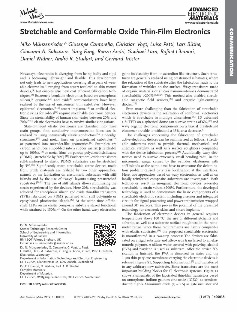
The fabrication of electronic devices in general requires temperatures above 100 °C, the use of different etchants and solvents, as well as a substrate surface roughness in the nano-meter range. Since these requirements are hardly compatible with elastic substrates, [ 28 ] the proposed stretchable electronics is manufactured in a two-step process: The devices are fabri-cated on a rigid substrate and afterwards transferred to an elas-tomeric polymer. A silicon wafer covered with polyvinyl alcohol (PVA) and parylene is used as substrate. After the device fab-rication is fi nished, the PVA is dissolved in water and the 1 µm-thin parylene membrane carrying the electronic devices is released (Figure S1, Supporting Information), [ 8 ] and transferred to any arbitrary new substrate. Since transistors are the most important building blocks for all electronic systems, Figure 1 a shows a schematic of the fabricated thin-fi lm transistors based on amorphous indium-gallium-zinc-oxide (IGZO) as semicon-ductor, high-k Aluminum oxide ( ε r ≈ 9.5) as gate insulator and
Nowadays, electronics is diverging from being bulky and rigid and is becoming lightweight and fl exible. This development not only leads to new applications covering all aspects of wear-able electronics, [ 1 ] ranging from smart textiles [ 2 ] to skin mount devices, [ 3 ] but enables also new cost effi cient fabrication tech-niques. [ 4 ] Extremely bendable electronics based on amorphous silicon, [ 5 ] organic, [ 6,7 ] and oxide [ 8 ] semiconductors have been realized by the use of micrometer thin substrates. However, epidermal electronics, [ 9,10 ] smart implants, [ 11 ] or artifi cial elec-tronic skins for robots [ 12 ] require stretchable electronic devices. Since the stretchability of human skin varies between 20% and 70%, [ 9,13 ] elastic electronics have to survive similar elongations.
State-of-the-art elastic electronics are classifi ed into three main groups: fi rst, conductive interconnection lines can be realized by using intrinsically elastic conductors, [ 14 ] air-bridge structures, [ 15 ] and metal lines on prestretched substrates [ 16 ] or patterned into meander-like geometries. [ 17 ] Examples are carbon nanotubes embedded into a rubber matrix (stretchable up to 100%), [ 14 ] or metal fi lms on porous polydimethylsiloxane (PDMS) (stretchable by 80%). [ 18 ] Furthermore, oxide transistors roll-transferred to elastic PDMS substrates can be stretched by 5%. [ 19 ] Signifi cantly more stretchable active devices made from brittle materials are realized by two other approaches, namely by the fabrication on elastomeric substrates with stiff islands and by the use of “wavy” layouts using prestretched substrates. [ 20,21 ] The use of stiff islands allows minimizing the strain experienced by the devices. Here 20% stretchability was achieved for amorphous silicon and oxide thin-fi lm transistors (TFTs) fabricated on PDMS patterned with stiff polyimide or epoxy-based photoresist islands. [ 22 ] At the same time off-the-shelf LEDs on an elastic composite substrate stayed functional while strained by 150%. [ 23 ] On the other hand, wavy electronics
www.MaterialsViews.com www.advelectronicmat.de
Adv. Electron. Mater. 2015, 1, 1400038
CO
MM
UN
ICATI
ON
© 2015 WILEY-VCH Verlag GmbH & Co. KGaA, Weinheim1400038 (2 of 7) wileyonlinelibrary.com
metals. [ 29,30 ] The mechanical properties of these devices are determined by the 1 µm-thin parylene membrane which ena-bles bending radii in the micrometer range (the IGZO TFTs survive mechanical strain of ≈1%). [ 8,31 ] This fl exibility and the low weight of the membrane are demonstrated in Figure 1 b,c, where the electronic membrane is transferred to the seeds of a dandelion. The electrical properties are determined by the mate-rials in the TFT stack. Even on this unconventional substrate, the IGZO TFTs exhibit a carrier mobility of 11.3 cm 2 V −1 s −1 and a threshold voltage of 0.4 V. The obtained mobility is sev-eral orders of magnitude higher than the mobility of organic semiconductors and amorphous silicon. [ 32 ] Additionally oxide semiconductors like IGZO are transparent and their amor-phous structure allows cost-effective deposition on large scale substrates. Hence the presented devices exhibit a set of proper-ties hardly achievable with other materials.
To guarantee the functionality of the electronics on a stretch-able substrate, it is necessary to ensure that the mechanical strains experienced by the presented oxide based electronic
devices always stays below ≈1%. [ 31 ] The high fl exibility and the possibility to transfer TFTs on a membrane to different sub-strates makes it possible to form wavy structures and to place them on composite substrates with stiff patches, whereas both approaches have advantages and disadvantages. [ 21 ]
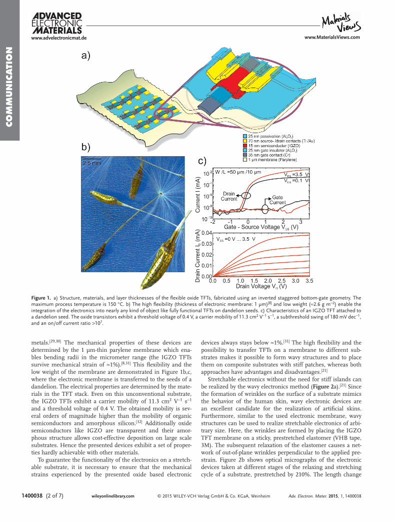
Stretchable electronics without the need for stiff islands can be realized by the wavy electronics method ( Figure 2 a). [ 21 ] Since the formation of wrinkles on the surface of a substrate mimics the behavior of the human skin, wavy electronic devices are an excellent candidate for the realization of artifi cial skins. Furthermore, similar to the used electronic membrane, wavy structures can be used to realize stretchable electronics of arbi-trary size. Here, the wrinkles are formed by placing the IGZO TFT membrane on a sticky, prestretched elastomer (VHB tape, 3M). The subsequent relaxation of the elastomer causes a net-work of out-of-plane wrinkles perpendicular to the applied pre-strain. Figure 2 b shows optical micrographs of the electronic devices taken at different stages of the relaxing and stretching cycle of a substrate, prestretched by 210%. The length change
www.MaterialsViews.comwww.advelectronicmat.de
Adv. Electron. Mater. 2015, 1, 1400038
Figure 1. a) Structure, materials, and layer thicknesses of the fl exible oxide TFTs, fabricated using an inverted staggered bottom-gate geometry. The maximum process temperature is 150 °C. b) The high fl exibility (thickness of electronic membrane: 1 µm) [ 8 ] and low weight (≈2.6 g m −2 ) enable the integration of the electronics into nearly any kind of object like fully functional TFTs on dandelion seeds. c) Characteristics of an IGZO TFT attached to a dandelion seed. The oxide transistors exhibit a threshold voltage of 0.4 V, a carrier mobility of 11.3 cm 2 V −1 s −1 , a subthreshold swing of 180 mV dec −1 , and an on/off current ratio >10 7 .

CO
MM
UN
ICATIO
N
© 2015 WILEY-VCH Verlag GmbH & Co. KGaA, Weinheim (3 of 7) 1400038wileyonlinelibrary.com
of the elastomeric substrate is used as a reference to calculate the strain, even if the length change of the TFT membrane is slightly smaller (≈150%). This is because the membrane is stiffer than the elastomer and the elastomer does not fully relax after being stretched. The good adhesion of the TFT membrane on the elastomer ensures that the wrinkles disappear nearly completely after restretching. The wrinkles were characterized by profi lometer and scanning electron microscope (SEM) meas-urements (Figure 2 c), they exhibit heights between 100 and 200 µm and a minimum bending radius of 40 µm. This bending radius induces ≈0.4% tensile strain into the TFT membrane and has no signifi cant infl uence on the electronics.
Figure 2 d shows the characteristics, and the corresponding evo-lution of the mobility and threshold voltage of a 210% stretched TFT after exposed to different levels of strain down to 0%. Although the length of the substrate changes by more than a factor of 3, the measurement resulted in a decrease of the threshold voltage by ≈90 mV, and a variation of the transistor mobility by <2%. Since the dimensions of the wrinkles are com-parable to the dimensions of the TFTs, which leads to a cov-erage of the individual TFTs under the wrinkles, TFTs on a fully relaxed substrate cannot be contacted. Corresponding measure-ments taken on the wrinkly surface of a partially relaxed sub-strate (and not after restretching) can be found in Figure S2,
www.MaterialsViews.com www.advelectronicmat.de
Adv. Electron. Mater. 2015, 1, 1400038
Figure 2. a) Realization of stretchable electronics using a wavy surface. b) Formation of wrinkles at different levels of strain: The electronic parylene membrane is attached to an elastomer prestretched by 210%. The membrane is well attached. If the strain is reduced wrinkles are formed on the surface, if the substrate is restretched the wrinkles disappear. c) SEM image and height profi le measurement of the wavy surface of a relaxed substrate (initial strain: 100%). Wrinkles are formed perpendicular to the initial strain, they exhibit an average height and width of ≈150 µm and ≈200 µm. d) Characteristics of a TFT (initial strain: 210%) measured at different strain values down to 0%. The performance parameter evolution shows that V TH shifts by <100 mV and µ varies by >2%. e) Infl uence of up to 2000 cycles of repeated stretching and relaxing of elastic TFTs (maximum an initial strain: 70%). The transfer characteristic and the corresponding performance parameter evolution show that the TFTs stay fully functional, whereas V TH and µ change by ≈200 mV and ≈2%. f) A 70% prestretched sticky tape with electronics on to the joint of a human thumb.
CO
MM
UN
ICATI
ON
© 2015 WILEY-VCH Verlag GmbH & Co. KGaA, Weinheim1400038 (4 of 7) wileyonlinelibrary.com
Supporting Information. To simulate the every-day use, the infl uence of multiple repetitions of elongation and relaxation was evaluated. For this cycling experiment, a maximum elonga-tion of 70% was chosen because this corresponds to the max-imum stretchability of human skin. [ 9,13 ] Figure 2 e illustrates the infl uence of repeated stretching and relaxation cycles on the TFT transfer characteristic and performance parameters. Up to 2000 stretching and relaxation cycles change the threshold voltage and mobility by only ≈50 mV and less than 4%. As visu-alized in Figure 2 f, where a 70% prestretched electronic sub-strate is attached to the joint of a human thumb, the presented wavy electronics can be employed to realize electronic patches and skins.
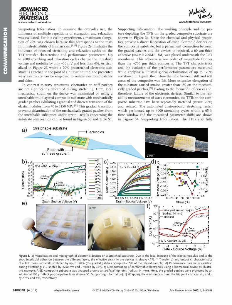
In contrast to wavy structures, electronics on stiff patches are not signifi cantly deformed during stretching. Here, local mechanical strain on the device was minimized by using a stretchable multilayered composite substrate with mechanically graded patches exhibiting a gradual and discrete transition of the elastic modulus from 40 to 5150 MPa. [ 23 ] This gradual transition prevents delamination of the mechanically graded patches from the stretchable substrates under strain. Details concerning the substrate composition can be found in Figure S3 and Table S1,
Supporting Information. The working principle and the pic-ture depicting the TFTs on the graded composite substrate are shown in Figure 3 a. Since the chemical and physical proper-ties prevent a direct fabrication of oxide electronic devices on the composite substrate, but a permanent connection between the graded patches and the devices is required, a 60 μm-thick adhesive (467MP 200MP, 3M) was placed underneath the TFT membrane. This adhesive is one order of magnitude thinner than the ≈700 µm thick composite. The TFT characteristics and the evolution of the performance parameters measured while applying a uniaxial global deformation of up to 120% are shown in Figure 3 b–d. Here the ratio between stiff and soft areas of the composite was 1:6. More extensive elongation of the substrate caused strains greater than 1% on the mechani-cally graded patches, [ 23 ] leading to the formation of cracks and, therefore, failure of the electronic devices. Similar to the reli-ability measurements of wavy electronics, the TFTs on the com-posite substrate have been repeatedly stretched (strain: 70%) and relaxed. The automated custom-build stretching tester, which performed up to 4000 stretching cycles within a 65 h time window and the measured parameter shifts are shown in Figure S4, Supporting Information. The TFTs stay fully
www.MaterialsViews.comwww.advelectronicmat.de
Adv. Electron. Mater. 2015, 1, 1400038
Figure 3. a) Visualization and micrograph of electronic devices on a stretched substrate. Due to the local increase of the elastic modulus and to the good interfacial adhesion between the different layers, the effective strain in the devices is always <1%. [ 23 ] Transfer b) and output c) characteristics of a TFT measured while stretched by up to 120% (the graded patches occupied ≈15% of the relaxed sample). d) Performance parameter variation during stretching: V TH shifted by <250 mV and µ varied by 37%. e) Demonstration of conformable electronics using a biomedical device as illustra-tive example: A 2D composite substrate was wrapped around an artifi cial hip joint (radius: 14 mm). Here, the graded patches were protected by an additional 100 µm-thick polypropylene layer (Figure S5, Supporting Information). f) Wrapping the electronics around the hip joint chances V TH and µ by 2 mV and 4%, respectively.
CO
MM
UN
ICATIO
N
© 2015 WILEY-VCH Verlag GmbH & Co. KGaA, Weinheim (5 of 7) 1400038wileyonlinelibrary.com
functional after this long-term cycling test and exhibit varia-tions of the threshold voltage and mobility of 170 mV and 20%, respectively.
In a next step, the presented concept was extended to a 2D substrate (Figure 3 e). 2D elastic electronics can be used to realize conformal electronic devices which can be wrapped around objects. Here, a spherical artifi cial hip joint with a radius of 14 mm was conformably covered with electronic devices. Since this deformation induces strain >120%, the elec-tronic devices were not directly attached to the graded patches but an additional 100 µm-thick polypropylene layer was placed between the TFT membrane and the elastic substrate. This additional layer increases the stretchability because the load transmission between parylene membrane and polypropylene is smaller than the load transmission to the parylene mem-brane directly glued to the composite substrate. The polypro-pylene layer protective layer enables elongations up to the sub-strate elasticity limit of 300% with only very little variations of the TFT performance parameters (Figure S5, Supporting Infor-mation). Consequently, the devices are virtually not affected from being wrapped around the hip joint (Figure 3 f).
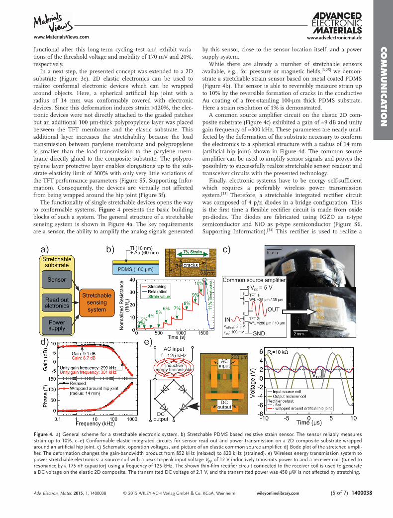
The functionality of single stretchable devices opens the way to conformable systems. Figure 4 presents the basic building blocks of such a system. The general structure of a stretchable sensing system is shown in Figure 4 a. The key requirements are a sensor, the ability to amplify the analog signals generated
by this sensor, close to the sensor location itself, and a power supply system.
While there are already a number of stretchable sensors available, e.g., for pressure or magnetic fi elds, [ 6,25 ] we demon-strate a stretchable strain sensor based on metal coated PDMS (Figure 4 b). The sensor is able to reversibly measure strain up to 10% by the reversible formation of cracks in the conductive Au coating of a free-standing 100-µm thick PDMS substrate. Here a strain resolution of 1% is demonstrated.
A common source amplifi er circuit on the elastic 2D com-posite substrate (Figure 4 c) exhibited a gain of ≈9 dB and unity gain frequency of ≈300 kHz. These parameters are nearly unaf-fected by the deformation of the substrate necessary to conform the electronics to a spherical structure with a radius of 14 mm (artifi cial hip joint) shown in Figure 4 d. The common source amplifi er can be used to amplify sensor signals and proves the possibility to successfully realize stretchable sensor readout and transceiver circuits with the presented technology.
Finally, electronic systems have to be energy self-suffi cient which requires a preferably wireless power transmission system. [ 33 ] Therefore, a stretchable integrated rectifi er circuit was composed of 4 p/n diodes in a bridge confi guration. This is the fi rst time a fl exible rectifi er circuit is made from oxide pn-diodes. The diodes are fabricated using IGZO as n-type semiconductor and NiO as p-type semiconductor (Figure S6, Supporting Information). [ 34 ] This rectifi er is used to realize a
www.MaterialsViews.com www.advelectronicmat.de
Adv. Electron. Mater. 2015, 1, 1400038
Figure 4. a) General scheme for a stretchable electronic system. b) Stretchable PDMS based resistive strain sensor. The sensor reliably measures strain up to 10%. c–e) Conformable elastic integrated circuits for sensor read out and power transmission on a 2D composite substrate wrapped around an artifi cial hip joint. c) Schematic, operation voltages, and picture of an elastic common source amplifi er. d) Bode plot of the stretched ampli-fi er. The deformation changes the gain-bandwidth product from 852 kHz (relaxed) to 820 kHz (strained). e) Wireless energy transmission system to power stretchable electronics: a source coil with a peak-to-peak input voltage V pp of 12 V inductively transmits power to and a receiver coil (tuned to resonance by a 175 nF capacitor) using a frequency of 125 kHz. The shown thin-fi lm rectifi er circuit connected to the receiver coil is used to generate a DC voltage on the elastic 2D composite. The transmitted DC voltage of 2.1 V, and the transmitted power was 450 µW is not affected by stretching.
CO
MM
UN
ICATI
ON
© 2015 WILEY-VCH Verlag GmbH & Co. KGaA, Weinheim1400038 (6 of 7) wileyonlinelibrary.com
www.MaterialsViews.comwww.advelectronicmat.de
Adv. Electron. Mater. 2015, 1, 1400038
stretchable, wireless power transmission system, and to supply energy to the elastic electronics conformed to the artifi cial hip joint. The energy is transmitted using two inductively coupled coils connected to the AC input of the elastic rectifi er (Figure 4 e). A source coil with a diameter of 8 cm and a receiver coil with a diameter of 4 cm (both fabricated using ten windings of 0.06 mm 2 Cu wire) were used. To minimize the energy absorbed by tissue, the system uses a carrier frequency of 125 kHz. [ 35 ] The demonstrated transmitted power of 450 μW is suffi cient to operate circuits based on IGZO TFTs. [ 30 ]
A potential application of the shown components is the strain based measurement of the body posture [ 36 ] using conformable strain sensing tags directly attached to the human body.
While the stiff island approach has not been further devel-oped here to enable connection between electronic compo-nents on different islands, numerous methods have been pro-posed to fabricate passive electrical interconnections on elastic substrates. Examples are CNTs, [ 14 ] air bridge structures, [ 15,37 ] horseshoe meander interconnects, [ 38 ] wavy metal lines, [ 39 ] or free fl oating interconnects. [ 10 ] A combination of stretchable con-ductive lines and active elements on graded islands can led to more complex stretchable systems in the future.
In summary, two different techniques for the fabrication of stretchable electronics based on high performance inorganic materials are presented. Oxide semiconductor based devices in a wavy layout as well as on a locally reinforced elastic com-posite substrate can be stretched by more than 200%. The subsequent expansion of the locally reinforced composite sub-strate approach into two dimensions led to the realization of conformable electronics that can be wrapped around any 3D shaped surfaces, such as an artifi cial hip joint. Wavy electronics at the same time mimic the wrinkling behavior of human skin and demonstrates the feasibility to combine soft biological systems with electronic functionality. Stretchable electronic components, in particular a strain sensor, an amplifi er cir-cuit for sensor read-out, and a wireless power transmission system, represent the basic building blocks of every stretchable sensor system and demonstrate the electrical performance and possible complexity of the proposed approach. All in all, the possibility to transform electronic devices made from brittle materials into a stretchable and conformal system proves the potential of the presented technology for smart skins and func-tionalized medical implants.
Experimental Section Device Fabrication: The fabrication of IGZO TFT is described in
ref. [ 8 ] . For the fabrication of diodes 5 nm Cr, 25 nm Cu, and 5 nm Ti were evaporated and structured into anode contacts. A 50 nm thick layer of IGZO was used n-type semiconductor. As p-type semiconductor 50 nm of NiO was DC sputtered at room temperature using a metallic Ni target and a 50% Ar, 50% O 2 atmosphere. The fabrication was fi nished by the deposition of 10 nm Ti and 75 nm Au as cathode contact. The stretchable PDMS based strain sensors were fabricated by replacing the 1 µm-thin parylene layer by 100 µm of spin coated PDMS. Afterwards an O 2 plasma and 10 nm Ti were used to improve the adhesion of a 60 nm-thick evaporated Au layer. After fabrication and release, the PDMS strain sensors were cut to a size of 4 × 35 mm 2 .
Transfer of Electronics to Stretchable Substrates: The fully manufactured sample was placed in water (fl oating). Within 120 min the water dissolved
a sacrifi cial PVA layer underneath the parylene/PDMS membrane and released the membrane with the electronic devices (Figure S1, Supporting Information). The stretchable composite substrates with mechanically graded patches were fabricated by solvent welding layers of polyurethane-based materials reinforced at progressively larger length scales. The elastic moduli of these materials are adjusted by the concentration of polyurethane hard domains at the molecular scale, laponite, and alumina platelets at the nano- and microscale (Table S1, Supporting Information). [ 23,40 ]
Characterization : Devices were characterized with probe tips under ambient condition using an Agilent B1500A. Sensors and TFTs were stretched using a custom-build stretching tester (Figure S4, Supporting Information). Performance parameters were extrapolated using the Shichman–Hodges model of the TFT current. [ 41 ] Circuits were characterized using an Agilent 33522A waveform generator and an Agilent MSO-X-3034A oscilloscope. Amplifi er measurements were performed using a load of 1 MΩ and 2 pF. Mechanical strain in the devices was calculated according to ref. [ 8 ] .
Supporting Information Supporting Information is available from the Wiley Online Library or from the author.
Acknowledgements This work was supported by the European Commission through the FP7 Project “fl exible multifunctional bendable integrated light-weight ultrathin systems” under contract no. FP7-287568.
Received: December 1, 2014 Revised: January 1, 2015
Published online: February 13, 2015
[1] A. Nathan , A. Ahnood , M. T. Cole , S. Lee , Y. Suzuki , P. Hiralal , F. Bonaccorso , T. Hasan , L. Garcia-Gancedo , A. Dyadyusha , S. Haque , P. Andrew , S. Hofmann , J. Moultrie , D. P. Chu , A. J. Flewitt , A. C. Ferrari , M. J. Kelly , J. Robertson , G. A. J. Amaratunga , W. I. Milne , Proc. IEEE 2012 , 100 , 1486 .
[2] K. Cherenack , C. Zysset , T. Kinkeldei , N. Münzenrieder , G. Tröster , Adv. Mater. 2010 , 22 , 5178 .
[3] a) Y. Y. Hsu , J. Hoffman , R. Ghaffari , B. Ives , P. H. Wei , L. Klinker , B. Morey , B. Elolampi , D. Davis , C. Rafferty , K. Dowling , presented at 7th Int. Microsystems, Packaging, Assembly and Circuits Tech-nology Conf. , Taipei , October 2012 ; b) H. Yung-Yu , C. Papakyrikos , M. Raj , M. Dalal , W. Pinghung , W. Xianyan , G. Huppert , B. Morey , R. Ghaffari , presented at 64th IEEE Electro nic Components and Technology Conf. Orlando , May 2014 .
[4] R. F. Service , Science 1997 , 278 , 383 . [5] E. Y. Ma , S. Wagner , Appl. Phys. Lett. 1999 , 74 , 2661 . [6] M. Kaltenbrunner , T. Sekitani , J. Reeder , T. Yokota , K. Kuribara ,
T. Tokuhara , M. Drack , R. Schwodiauer , I. Graz , S. Bauer-Gogonea , S. Bauer , T. Someya , Nature 2013 , 499 , 458 .
[7] T. Sekitani , U. Zschieschang , H. Klauk , T. Someya , Nat. Mater. 2010 , 9 , 1015 .
[8] G. A. Salvatore , N. Münzenrieder , T. Kinkeldei , L. Petti , C. Zysset , I. Strebel , L. Büthe , G. Tröster , Nat. Commun. 2014 , 5 , 2982 .
[9] T. Sekitani , T. Someya , MRS Bull. 2012 , 37 , 236 . [10] S. Xu , Y. H. Zhang , L. Jia , K. E. Mathewson , K. I. Jang , J. Kim ,
H. R. Fu , X. Huang , P. Chava , R. H. Wang , S. Bhole , L. Z. Wang ,

CO
MM
UN
ICATIO
N
© 2015 WILEY-VCH Verlag GmbH & Co. KGaA, Weinheim (7 of 7) 1400038wileyonlinelibrary.com
www.MaterialsViews.com www.advelectronicmat.de
Adv. Electron. Mater. 2015, 1, 1400038
Y. J. Na , Y. Guan , M. Flavin , Z. S. Han , Y. G. Huang , J. A. Rogers , Science 2014 , 344 , 70 .
[11] a) Y. W. Su , Z. J. Liu , S. D. Wang , R. Ghaffari , D. H. Kim , K. C. Hwang , J. A. Rogers , Y. G. Huang , Int. J. Solids Struct. 2014 , 51 , 1555 ; b) J. Reeder , M. Kaltenbrunner , T. Ware , D. Arreaga-Salas , A. Avendano-Bolivar , T. Yokota , Y. Inoue , M. Sekino , W. Voit , T. Sekitani , T. Someya , Adv. Mater. 2014 , 26 , 4967 .
[12] S. Bauer , Nat. Mater. 2013 , 12 , 871 . [13] F. Axisa , D. Brosteaux , E. De Leersnyder , F. Bossuyt , J. Vanfl eteren ,
B. Hermans , R. Puers , in Proc. Engineering in Medicine and Biology Society, IEEE, Piscataway, NJ 2007 , 5687 .
[14] T. Sekitani , H. Nakajima , H. Maeda , T. Fukushima , T. Aida , K. Hata , T. Someya , Nat. Mater. 2009 , 8 , 494 .
[15] D. Y. Khang , J. A. Rogers , H. H. Lee , Adv. Funct. Mater. 2009 , 19 , 1526 .
[16] S. P. Lacour , J. Jones , S. Wagner , T. Li , Z. G. Suo , Proc. IEEE 2005 , 93 , 1459 .
[17] K. L. Lin , K. Jain , IEEE Electron Device Lett. 2009 , 30 , 14 . [18] G. S. Jeong , D. H. Baek , H. C. Jung , J. H. Song , J. H. Moon ,
S. W. Hong , I. Y. Kim , S. H. Lee , Nat. Commun. 2012 , 3 , 977. [19] B. K. Sharma , B. Jang , J. E. Lee , S. H. Bae , T. W. Kim , H. J. Lee ,
J. H. Kim , J. H. Ahn , Adv. Funct. Mater. 2013 , 23 , 2024 . [20] D. H. Kim , J. A. Rogers , Adv. Mater. 2008 , 20 , 4887 . [21] D. Y. Khang , H. Q. Jiang , Y. Huang , J. A. Rogers , Science 2006 , 311 , 208 . [22] a) S. P. Lacour , I. Graz , D. Cotton , S. Bauer , S. Wagner , in Proc.
Ann. Int. Eng. Med. Biol. IEEE EMBS, Boston , IEEE, Piscataway, NJ 2011 , 8373 ; b) A. Romeo , Q. Liu , Z. Suo , S. P. Lacour , Appl. Phys. Lett. 2013 , 102 , 131904 ; c) K. Park , D. K. Lee , B. S. Kim , H. Jeon , N. E. Lee , D. Whang , H. J. Lee , Y. J. Kim , J. H. Ahn , Adv. Funct. Mater. 2010 , 20 , 3577 .
[23] R. Libanori , R. M. Erb , A. Reiser , H. Le Ferrand , M. J. Suess , R. Spolenak , A. R. Studart , Nat. Commun. 2012 , 3 , 1265 .
[24] J. A. Rogers , MRS Bull. 2014 , 39 , 549 . [25] M. Melzer , G. G. Lin , D. Makarov , O. G. Schmidt , Adv. Mater. 2012 ,
24 , 6468 . [26] M. S. White , M. Kaltenbrunner , E. D. Glowacki , K. Gutnichenko ,
G. Kettlgruber , I. Graz , S. Aazou , C. Ulbricht , D. A. M. Egbe , M. C. Miron , Z. Major , M. C. Scharber , T. Sekitani , T. Someya , S. Bauer , N. S. Sariciftci , Nat. Photonics 2013 , 7 , 811 .
[27] P. I. Hsu , H. Gleskova , M. Huang , Z. Suo , S. Wagner , J. C. Sturm , J. Non-Cryst. Solids 2002 , 299 , 1355 .
[28] R. M. Erb , K. H. Cherenack , R. E. Stahel , R. Libanori , T. Kinkeldei , N. Münzenrieder , G. Tröster , A. R. Studart , ACS Appl. Mater. Inter. 2012 , 4 , 2860 .
[29] K. Nomura , H. Ohta , A. Takagi , T. Kamiya , M. Hirano , H. Hosono , Nature 2004 , 432 , 488 .
[30] N. Münzenrieder , L. Petti , C. Zysset , G. A. Salvatore , T. Kinkeldei , C. Perumal , C. Carta , F. Ellinger , G. Tröster , in Proc. IEEE Int. Electron Devices Meeting, IEEE, Piscataway, NJ 2012 , 5.2.1 .
[31] N. Münzenrieder , L. Petti , C. Zysset , D. Görk , L. Büthe , G. A. Salvatore , G. Tröster , in Proc. European Solid-State Develop-ment and Research Conf. , IEEE, Piscataway, NJ 2013 , 362 .
[32] a) P. Barquinha , L. Pereira , G. Goncalves , R. Martins , E. Fortunato , Electrochem. Solid-State Lett. 2008 , 11 , H248 ; b) F. Ante , D. Kalblein , T. Zaki , U. Zschieschang , K. Takimiya , M. Ikeda , T. Sekitani , T. Someya , J. N. Burghartz , K. Kern , H. Klauk , Small 2012 , 8 , 73 ; c) K. H. Cherenack , A. Z. Kattamis , B. Hekmashoar , J. C. Sturm , S. Wagner , J. Korean Phys. Soc. 2009 , 54 , 415 .
[33] T. Sekitani , M. Takamiya , Y. Noguchi , S. Nakano , Y. Kato , T. Sakurai , T. Someya , Nat. Mater. 2007 , 6 , 413 .
[34] N. Münzenrieder , C. Zysset , L. Petti , T. Kinkeldei , G. A. Salvatore , G. Tröster , Solid-State Electron 2013 , 87 , 17 .
[35] W. Peijun , T. Yina , G. Kunling , W. Guoxing , D. Simin , S. Guofang , R. Yuefeng , L. Jingquan , presented at 4th Int. Conf. Biomedical Engineering and Biotechnology , Shanghai , October 2011 .
[36] C. Mattmann , O. Amft , H. Harms , G. Troster , presented at 11th IEEE Symp. Wearable Computers , Boston , October 2007 .
[37] J. Song , Y. Huang , J. Xiao , S. Wang , K. C. Hwang , H. C. Ko , D. H. Kim , M. P. Stoykovich , J. A. Rogers , J. Appl. Phys. 2009 , 105 , 123516 .
[38] M. Gonzalez , F. Axisa , M. V. BuIcke , D. Brosteaux , B. Vandevelde , J. Vanfl eteren , Microelectron. Reliab. 2008 , 48 , 825 .
[39] J. Jones , S. P. Lacour , S. Wagner , Z. G. Suo , J. Vac. Sci. Technol. A 2004 , 22 , 1723 .
[40] R. Libanori , F. H. L. Munch , D. M. Montenegro , A. R. Studart , Compos. Sci. Technol. 2012 , 72 , 435 .
[41] S. M. Sze , K. K. Ng , Physics of Semiconductor Devices , John Wiley and Sons , Hoboken, NJ 2007 .
Related Documents


