CANTONI ET AL. VOL. 5 ’ NO. 6 ’ 4783–4789 ’ 2011 www.acsnano.org 4783 May 24, 2011 C 2011 American Chemical Society Strain-Driven Oxygen Deficiency in Self-Assembled, Nanostructured, Composite Oxide Films Claudia Cantoni, †, * Yanfei Gao, ‡,§ Sung Hun Wee, † Eliot D. Specht, † Jaume Gazquez, † Jianyong Meng, § Stephen J. Pennycook, † and Amit Goyal † † Materials Science and Technology Division, Oak Ridge National Laboratory, Oak Ridge, Tennessee 37831-6116, Unites States, ‡ Computer Science and Mathematics Division, Oak Ridge National Laboratory, Oak Ridge, Tennessee 37831-6164, United States, and § Department of Materials Science and Engineering, University of Tennessee, Knoxville, Tennessee 37996-2200, United States. W ithin the field of metal oxides, nanocomposite films with novel functionality have been recently synthesized by spontaneous assembly of nanodots or nanorods of one material em- bedded in the matrix of another material. 17 This approach has been successfully em- ployed to fabricate multiferroics and magne- toelectric nanocomposites by coupling ferroelectric and magnetostrictive compo- nents for application in spintronics, informa- tion storage, and logic devices. 13 Other successful applications include thermoelec- tric composites 4 and high-T c superconduc- tors, in which enhanced performance is obtained by self-assembly of nonsupercon- ducting oxide nanorods within the super- conductor matrix. 5,6 The latter nanocomposite system is of general interest as a model for other oxide-based nanocomposites in which enhanced or novel functionality arises from strain coupling of the constituent phases. As oxide-based nanocomposites form a new and very incomplete area of research, little is known about the relationships between func- tionality, nanocomposite microstructure, and strain and composition modulations at the nanoscale. Nanocomposites incorporating superconductors can be useful in advancing our fundamental understanding of functional oxide nanocomposites in general because of the wealth of existing knowledge about super- conductive properties and the way they change with the addition of nanosized corre- lated defects and second phases. For example, flux pinning and critical current are well- known to be extremely sensitive not only to shape, order, and size of embedded nanopar- ticles but also to more subtle changes in interfacial composition and lattice defects on a subnanometer scale. Here we present a detailed investigation of interfacial structure and chemistry in composite films made of BaZrO 3 (BZO) self-assembled nanocolumns within a RE- Ba 2 Cu 3 O 7-δ (REBCO; RE: rare earth, Y, or mixture of Y and rare earth) high-T c super- conductive matrix. We combine finite ele- ment and analytical strain field calculations, X-ray diffraction (XRD), and atomic resolu- tion Z-contrast scanning transmission elec- tron microscopy (Z-STEM) coupled with electron energy loss spectroscopy (EELS) to show that the local strain induces oxygen deficiency in the superconductive matrix, which leads to a significant reduction in the long-range superconducting properties. The region of degraded superconductivity extends for several nanometers around each nanocolumn, implying that a maxi- mum useful density exists for optimized properties. On the basis of these findings, we propose impurity doping as a mean to relieve strain and suppress formation of O vacancies, thereby improving superconduc- tivity around the nanocolumns. The mechanism responsible for solid- state self-assembly is largely related to the strain field that develops around the nano- scale second phases embedded in the * Address correspondence to [email protected]. Received for review February 24, 2011 and accepted May 24, 2011. Published online 10.1021/nn2007628 ABSTRACT Oxide self-assembly is a promising bottom-up approach for fabricating new composite materials at the nanometer length scale. Tailoring the properties of such systems for a wide range of electronic applications depends on the fundamental understanding of the interfaces between the constituent phases. We show that the nanoscale strain modulation in self-assembled systems made of high-T c superconducting films containing nanocolumns of BaZrO 3 strongly affects the oxygen composition of the superconductor. Our findings explain the observed reduction of the superconducting critical temperature. KEYWORDS: self-assembly . thin-film nanocomposites . nanorods . strain . superconductors . scanning transmission electron microscopy ARTICLE

Welcome message from author
This document is posted to help you gain knowledge. Please leave a comment to let me know what you think about it! Share it to your friends and learn new things together.
Transcript

CANTONI ET AL. VOL. 5 ’ NO. 6 ’ 4783–4789 ’ 2011
www.acsnano.org
4783
May 24, 2011
C 2011 American Chemical Society
Strain-Driven Oxygen Deficiency inSelf-Assembled, Nanostructured,Composite Oxide FilmsClaudia Cantoni,†,* Yanfei Gao,‡,§ Sung Hun Wee,† Eliot D. Specht,† Jaume Gazquez,† Jianyong Meng,§
Stephen J. Pennycook,† and Amit Goyal†
†Materials Science and Technology Division, Oak Ridge National Laboratory, Oak Ridge, Tennessee 37831-6116, Unites States, ‡Computer Science and MathematicsDivision, Oak Ridge National Laboratory, Oak Ridge, Tennessee 37831-6164, United States, and §Department of Materials Science and Engineering, University ofTennessee, Knoxville, Tennessee 37996-2200, United States.
Within the field of metal oxides,nanocomposite films with novelfunctionality have been recently
synthesized by spontaneous assembly ofnanodots or nanorods of one material em-bedded in thematrix of another material.1�7
This approach has been successfully em-ployed to fabricatemultiferroics andmagne-toelectric nanocomposites by couplingferroelectric and magnetostrictive compo-nents for application in spintronics, informa-tion storage, and logic devices.1�3 Othersuccessful applications include thermoelec-tric composites4 and high-Tc superconduc-tors, in which enhanced performance isobtained by self-assembly of nonsupercon-ducting oxide nanorods within the super-conductormatrix.5,6 The latter nanocompositesystem is of general interest as a model forother oxide-based nanocomposites in whichenhanced or novel functionality arises fromstrain coupling of the constituent phases. Asoxide-based nanocomposites form a new andvery incomplete area of research, little isknown about the relationships between func-tionality, nanocomposite microstructure, andstrain and composition modulations at thenanoscale. Nanocomposites incorporatingsuperconductors can be useful in advancingour fundamental understanding of functionaloxide nanocomposites in general because ofthewealthof existingknowledgeabout super-conductive properties and the way theychange with the addition of nanosized corre-lateddefects and secondphases. For example,flux pinning and critical current are well-known to be extremely sensitive not only toshape, order, and size of embedded nanopar-ticles but also to more subtle changes ininterfacial composition and lattice defects ona subnanometer scale.
Here we present a detailed investigationof interfacial structure and chemistry incomposite films made of BaZrO3 (BZO)self-assembled nanocolumns within a RE-Ba2Cu3O7-δ (REBCO; RE: rare earth, Y, ormixture of Y and rare earth) high-Tc super-conductive matrix. We combine finite ele-ment and analytical strain field calculations,X-ray diffraction (XRD), and atomic resolu-tion Z-contrast scanning transmission elec-tron microscopy (Z-STEM) coupled withelectron energy loss spectroscopy (EELS)to show that the local strain induces oxygendeficiency in the superconductive matrix,which leads to a significant reduction in thelong-range superconducting properties.The region of degraded superconductivityextends for several nanometers aroundeach nanocolumn, implying that a maxi-mum useful density exists for optimizedproperties. On the basis of these findings,we propose impurity doping as a mean torelieve strain and suppress formation of Ovacancies, thereby improving superconduc-tivity around the nanocolumns.The mechanism responsible for solid-
state self-assembly is largely related to thestrain field that develops around the nano-scale second phases embedded in the
* Address correspondence [email protected].
Received for review February 24, 2011and accepted May 24, 2011.
Published online10.1021/nn2007628
ABSTRACT Oxide self-assembly is a promising bottom-up approach for fabricating new
composite materials at the nanometer length scale. Tailoring the properties of such systems for
a wide range of electronic applications depends on the fundamental understanding of the interfaces
between the constituent phases. We show that the nanoscale strain modulation in self-assembled
systems made of high-Tc superconducting films containing nanocolumns of BaZrO3 strongly affects
the oxygen composition of the superconductor. Our findings explain the observed reduction of the
superconducting critical temperature.
KEYWORDS: self-assembly . thin-film nanocomposites . nanorods . strain .superconductors . scanning transmission electron microscopy
ARTIC
LE

CANTONI ET AL. VOL. 5 ’ NO. 6 ’ 4783–4789 ’ 2011
www.acsnano.org
4784
matrix and to the reduction of phase boundary energy.Theoretical formulations based on energetic andkinetic arguments (which will be discussed in detailin a future publication) specify an optimal range of4�12% for the lattice mismatch of the embeddedphase with respect to the REBCO matrix. The resultingnanocolumns extend for nearly the entire film thick-ness and consist of long, continuous nanorods orstacks of shorter nanorods.The ordered array of BZO nanocolumns in REBCO
was obtained by simultaneous deposition of REBCOand BZO either by performing laser ablation from aBZO-doped YBCO target or by adding Zr to the liquidprecursor in ametal organic chemical vapor deposition(MOCVD) reactor. Details of film deposition are re-ported elsewhere.8,9 All composite films were grownepitaxially on biaxially textured, buffered hastelloytapes.10 STEM and EELS data were acquired in adedicated STEM, VG Microscopes HB501UX, operatedat 100 kV and equipped with an Enfina EEL spectro-meter and a Nion aberration corrector.Figure 1A shows themicrostructure of a 0.8 μmthick,
4 vol % BZO-doped YBCO film made via pulsed laserdeposition (PLD). A mismatch of ∼8% is found be-tween three BZO perovskite unit cells (a = 4.193 Å) andthe tripled perovskite blocks that make up the YBCOcell. The mismatch occurs along the vertical interfacesbetween the nanocolumns and the matrix with theepitaxial relationship BZO(001)//YBCO(001)//surfacenormal; BZO(100)//YBCO(100). The out-of-plane straindistribution that arises from this misfit can be calcu-lated by a finite element method and is shown inFigure 1B,C for two values of the ratio between nano-column length, d, and distance between nanocolumns,L, representing the cases of a dilute and concentrateddistribution of BZO nanocolumns in the host matrix,respectively. The films considered here fall in theconcentrated limit of Figure 1C. When panels B and Cof Figure 1 are compared, it is evident that an increasedconcentration of BZO nanocolumns leads to a largeroverall positive strain of the REBCO along the c axis,resulting in an average increase of the c lattice para-meter. In real systems, misfit dislocations form at theinterfaces around precipitates and affect the localstrain field together with inhomogeneities in cationor oxygen composition. The microstrain in each com-posite film can be measured via XRD by analyzing thewidth of multiple REBCO Bragg peaks displayed in aWilliamson�Hall plot.11 As expected, the microstrainalso increases with increasing BZO concentration, asshown in Figure 1D, where a comparison is madebetween simulated strain and strain extracted byXRD as a function of BZO volume fraction. As the plotshows, the experimental slope is reduced to nearly24% of the simulation for the case d/L = 20 andcoherent interface, indicating that 76% of the originalmisfit has been relieved and the effective residual
misfit strain is ∼24% � 8% = 1.9%. This reduction iscaused by misfit dislocations that form at the YBCO/BZO interface, giving rise to a semicoherent REBCO/BZO phase boundary. Figure 1D also shows the straincalculated by finite element simulation in the presenceofmisfit dislocations at the BZO/YBCO phase boundaryfor the less computationally intensive case of d/L = 1.These values aremuch closer to the experimental data,further supporting the presence of interface disloca-tions in the system. The incoherent phase boundary ismodeled by solving the lattice disregistry field and thusdetermining the defect density from the balance of thedisregistry-induced interplanar energy and the long-range elastic interaction.12
In addition to an increase in strain, a nearly linearreduction of Tc is observed with increasing BZO con-centration that amounts to roughly 0.4 K for unitarychange in BZO concentration expressed in vol %.Figure 2 shows the superconducting critical tempera-ture obtained through four-probe resistive measure-ments for PLD and MOCVD films as a function of theBZO concentration measured by XRD. Both PLD andMOCVD films show a similar decrease in Tc withincreasing BZO concentration as better visualized bythe plot of ΔTc shown in Figure 2B. We note thatvariations as large as 0.5 K are typically observed forthe Tc of nominally identical REBCO films. Therefore,the present data do not provide a definitive answer forthe behavior of Tc at small BZO concentrations up to∼4 vol %. However, above this concentration, thedecrease in Tc is clearly larger than any sample-to-sample variation.For atomic scale information on structure and com-
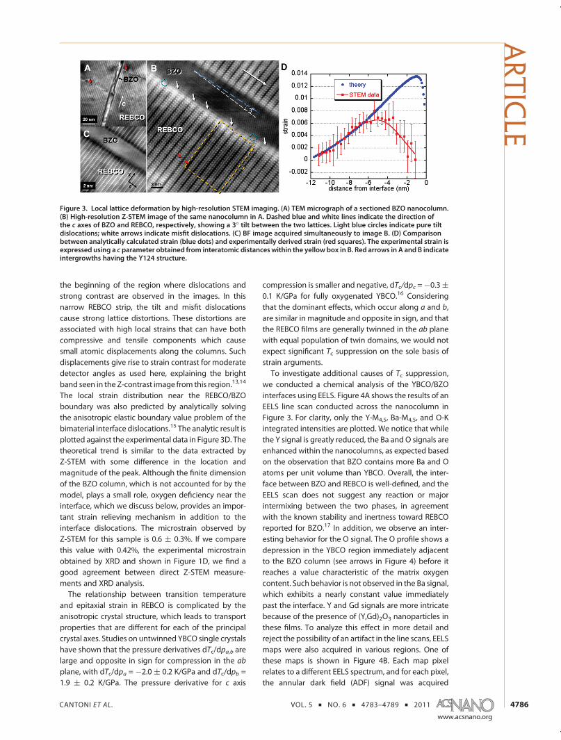
position, we use aberration-corrected Z-STEM coupledwith EELS. The BZO nanocolumns have a width of6�8 nm, while our typical TEM foils, prepared by thefocused ion beam technique, have a thickness of about30�40 nm. Consequently, in most TEM samples, theBZO nanocolumns are covered by several REBCOatomic planes, and this superimposition results inmoir�e fringes rather than clear BZO lattice fringes(see Figure 1A). In the case of Figure 3, a single BZOrod has been sectioned by the TEM preparation pro-cess along most of its entire length, offering theopportunity to view the details of its interface withthe REBCO lattice. For this particular MOCVD film, theBZO volume fraction, as measured by X-rays, is 4.1%and RE is a mixture of Y and Gd. Figure 3B is a high-resolution Z-STEM micrograph of the nanocolumn inFigure 3A and clearly shows that the BZO c axis and theREBCO c axis are tilted with respect to each other bynearly 3�. This commonly observed tilt is accommo-dated by introduction of dislocations, some of whichare pure tilt dislocations with Burgers vector 1/2(100),as indicated by circles. The images also reveal misfitdislocations with Burgers vector 1/2(101), which areactive in relievingmisfit strain (arrows in Figure 3B). The
ARTIC
LE

CANTONI ET AL. VOL. 5 ’ NO. 6 ’ 4783–4789 ’ 2011
www.acsnano.org
4785
average spacing between these dislocations is ∼3YBCO unit cells (3.5 nm). A similar average spacing D
can be calculated using the equation D = bz/(fo � εo),where fo defines the original misfit between lattices, εois the residual misfit strain, and bz is the Burgers vectorcomponent along the interface plane. Choosing εo =1.9% as calculated above, gives D = 2.7 YBCO unit cells,showing excellent agreement between STEM and XRDresults. The REBCO lattice surrounding the BZO nano-rod shows a brighter contrast than the REBCO wellwithin thematrix. The same region gives an even larger(and inverted) contrast in the bright field (BF) imageacquired simultaneously to Figure 3B (see Figure 3C),strongly suggesting the presence of significant strainlocalized in the REBCO lattice surrounding the BZOnanocolumn.
The local strain can be quantified directly throughthe Z-STEM images by measuring the variation of theREBCO c axis parameter. Figure 3D shows the result ofsuch a measurement where the c axis spacing isobtained by fitting Gaussian curves to the intensity ofthe Ba and Y/Gd columns in the dashed box ofFigure 3B. About 13 values for c were calculated ateach basal unit cell increment along the x direction andthe average ch plotted in Figure 3D as (ch� co)/co, whereco is the c parameter well within the matrix. Themeasured strain increases when moving from thematrix interior toward the BZO nanorod until it reachesa maximum at a distance of∼5 nm from the interface.Then, in close proximity to the BZO interface, the straindecreases rapidly over a distance of about 3 nm. Theend part of the plot, around x =�2 nm, corresponds to
Figure 1. Evaluation of strain in BZO-doped REBCO composite films. (A) TEM micrograph illustrating the morphology of a4 vol % BZO nanocolumn array embedded in the YBCO matrix. (B,C) Volumetric average of the out-of-plane strain (ε33/fo;fo= lattice misfit) calculated through finite element method for the cases d/L = 1 (B) and d/L = 20 (C). (D) Strain versus BZOconcentration as calculated by the finite element method for the cases d/L = 20 coherent interface (blue triangles), d/L = 1coherent interface (black dots), d/L = 1 incoherent interface (black circles), and measured by X-ray diffraction for PLD films(red, open squares) and MOCVD films (red, filled squares).
Figure 2. Critical temperature (Tc) obtained by resistivity vs temperature measurements for PLD and MOCVD BZO-dopedREBCO films. (A) Tc dependence on BZO concentration. (B) Plot of variations of Tc (ΔTc) with respect to the Tc of undopedREBCO samples.
ARTIC
LE
CANTONI ET AL. VOL. 5 ’ NO. 6 ’ 4783–4789 ’ 2011
www.acsnano.org
4786
the beginning of the region where dislocations andstrong contrast are observed in the images. In thisnarrow REBCO strip, the tilt and misfit dislocationscause strong lattice distortions. These distortions areassociated with high local strains that can have bothcompressive and tensile components which causesmall atomic displacements along the columns. Suchdisplacements give rise to strain contrast for moderatedetector angles as used here, explaining the brightband seen in the Z-contrast image from this region.13,14
The local strain distribution near the REBCO/BZOboundary was also predicted by analytically solvingthe anisotropic elastic boundary value problem of thebimaterial interface dislocations.15 The analytic result isplotted against the experimental data in Figure 3D. Thetheoretical trend is similar to the data extracted byZ-STEM with some difference in the location andmagnitude of the peak. Although the finite dimensionof the BZO column, which is not accounted for by themodel, plays a small role, oxygen deficiency near theinterface, which we discuss below, provides an impor-tant strain relieving mechanism in addition to theinterface dislocations. The microstrain observed byZ-STEM for this sample is 0.6 ( 0.3%. If we comparethis value with 0.42%, the experimental microstrainobtained by XRD and shown in Figure 1D, we find agood agreement between direct Z-STEM measure-ments and XRD analysis.The relationship between transition temperature
and epitaxial strain in REBCO is complicated by theanisotropic crystal structure, which leads to transportproperties that are different for each of the principalcrystal axes. Studies on untwinned YBCO single crystalshave shown that the pressure derivatives dTc/dpa,b arelarge and opposite in sign for compression in the ab
plane, with dTc/dpa = �2.0 ( 0.2 K/GPa and dTc/dpb =1.9 ( 0.2 K/GPa. The pressure derivative for c axis
compression is smaller and negative, dTc/dpc =�0.3(0.1 K/GPa for fully oxygenated YBCO.16 Consideringthat the dominant effects, which occur along a and b,are similar in magnitude and opposite in sign, and thatthe REBCO films are generally twinned in the ab planewith equal population of twin domains, we would notexpect significant Tc suppression on the sole basis ofstrain arguments.To investigate additional causes of Tc suppression,
we conducted a chemical analysis of the YBCO/BZOinterfaces using EELS. Figure 4A shows the results of anEELS line scan conducted across the nanocolumn inFigure 3. For clarity, only the Y-M4,5, Ba-M4,5, and O-Kintegrated intensities are plotted. We notice that whilethe Y signal is greatly reduced, the Ba and O signals areenhanced within the nanocolumns, as expected basedon the observation that BZO contains more Ba and Oatoms per unit volume than YBCO. Overall, the inter-face between BZO and REBCO is well-defined, and theEELS scan does not suggest any reaction or majorintermixing between the two phases, in agreementwith the known stability and inertness toward REBCOreported for BZO.17 In addition, we observe an inter-esting behavior for the O signal. The O profile shows adepression in the YBCO region immediately adjacentto the BZO column (see arrows in Figure 4) before itreaches a value characteristic of the matrix oxygencontent. Such behavior is not observed in the Ba signal,which exhibits a nearly constant value immediatelypast the interface. Y and Gd signals are more intricatebecause of the presence of (Y,Gd)2O3 nanoparticles inthese films. To analyze this effect in more detail andreject the possibility of an artifact in the line scans, EELSmaps were also acquired in various regions. One ofthese maps is shown in Figure 4B. Each map pixelrelates to a different EELS spectrum, and for each pixel,the annular dark field (ADF) signal was acquired
Figure 3. Local lattice deformation by high-resolution STEM imaging. (A) TEM micrograph of a sectioned BZO nanocolumn.(B) High-resolution Z-STEM image of the same nanocolumn in A. Dashed blue and white lines indicate the direction ofthe c axes of BZO and REBCO, respectively, showing a 3� tilt between the two lattices. Light blue circles indicate pure tiltdislocations; white arrows indicate misfit dislocations. (C) BF image acquired simultaneously to image B. (D) Comparisonbetween analytically calculated strain (blue dots) and experimentally derived strain (red squares). The experimental strain isexpressed using a c parameter obtained from interatomic distanceswithin the yellow box in B. Red arrows in A and B indicateintergrowths having the Y124 structure.
ARTIC
LE

CANTONI ET AL. VOL. 5 ’ NO. 6 ’ 4783–4789 ’ 2011
www.acsnano.org
4787
simultaneously with the EELS data, as shown in the topimage of Figure 4B. Analogously to Figure 3B, the ADFsignal shows a large intensity (bright contrast) in theREBCO region immediately adjacent to the BZO rod.The region showing the brightest shade in the ADFmap appears as darkest in the O-K map (see secondimage from top in Figure 4B). The O signal shows amaximum value in the interior of the BZO rod, aminimum value in the YBCO region immediately sur-rounding the rod, and an intermediate value furtheraway from the BZO rod. In contrast, the Ba andCumapsshow maximum and minimum values, respectively,within the BZO rod and exhibit a constant contrastlevel everywhere else in the surrounding REBCO ma-trix. Since the ADF signal is not sensitive to light speciessuch as O and the heavier atoms show a constantconcentration outside the BZO rod, the bright contrastin the ADF map should be related to strain. The darkcontrast in the O map cannot be determined bydechanneling and high-angle scattering of a portionof the incident electron beam, which is therefore notcollected by the EELS detector. If this were the case, asimilar dark contrast would be observed in the cationmaps as well. These observations not only confirm theline scan findings but also suggest, through the corre-lation between ADF andO signals, that the strain in the
REBCO lattice surrounding the BZO rod and the oxygendeficiency are correlated. As an alternative method todetect oxygen deficiency, we probed the Cu valencestate byanalyzing theCu-L2,3 edgewell inside theREBCOmatrix and in the region adjacent to the BZO rod.18
Figure 4C shows this analysis performed for twodifferentregions in the spectrum image in Figure 4B. As shownbythe ratio of the L3 and L2 lines, the Cu valence is lower inregion 1, adjacent to the BZO rod than in region 2,withinthe REBCO matrix. The same behavior for the Cu-L2,3edges is observed in all of the spectrum images acquiredand independently on the number of pixels chosen forregions 1 and 2, indicating that the oxygen deficiency ispresent everywherewithin the strained region surround-ing the nanorods and is not localized in certain points.It is important to point out that depletion of oxygen
in the REBCO phase by the more thermodynamicallystable BZO phase is unlikely because all of the REBCOfilms analyzed here were grown at an oxygen pressurewell above the equilibrium pressure for REBCO stabi-lity. In addition, BZO-free REBCO films grown in thesame conditions as the films analyzed here did notshow any evidence of oxygen deficiency. The oxygendeficiency observed here is likely the consequence ofthe high strain experienced by the YBCO lattice in thedislocation-decorated region at the BZO interface,
Figure 4. Results of EELS analysis. (A) Integrated intensity profiles of Y-M4,5, O-K, and Ba-M4,5 across the BZO nanocolumnof Figure 3. (B) EELS maps of O-K, Ba-M4,5, Cu-L2,3, and Gd-M4,5. The top map is the signal from the ADF detector acquiredsimultaneously to each spectrum. The yellow arrows highlight the suppressed O signal in proximity of the nanocolumn.(C) Comparison of Cu-L2,3 edges after removal of plural scattering by deconvolution for the regions labeled 1 and 2 in B.
ARTIC
LE

CANTONI ET AL. VOL. 5 ’ NO. 6 ’ 4783–4789 ’ 2011
www.acsnano.org
4788
similarly to what has been reported for YBCO grainboundaries.19 Within this picture, the strain wouldhinder proper REBCOoxygenation, and this substoichio-metry would, in turn, lower the strain near the phaseboundary, partially explaining the discrepancy withanalytical calculations (Figure 3D). The existence of arelationship between film stress and oxygen nonstoi-chiometry has already been reported by others.20,21
The overall conclusion from the O maps and linescans is that the oxygen-deficient REBCO stretches overa region of outer diameter equal to 3�4 times the BZOrod diameter. It is known that oxygen deficiency readilysuppresses Tc in REBCO.22 Considering that the dia-meter of the BZO rods are 6�8 nm and the averagespacing between BZO rods is ∼20 nm for a BZOconcentration of 4 vol %, an overlap of oxygen-de-pleted REBCO regions surrounding BZO nanocolumnsis expected to occur near or above this concentration,
leading to thedisruptionof current percolation throughthe high Tc phase and, consequently, to a lower mea-sured Tc. Disruption of current percolation above acertain BZO concentration is likely to occur in our self-assembled BZO�REBCO systems, in which the BZOrods are distributed with a high degree of order withinthe REBCO matrix.23
We have shown direct evidence of microstrain andits resulting effect on anion composition. The strain islocalized around the BZO nanocolumns over distancesof a few nanometers. EELS spectrum imaging showsoxygen deficiency within the strained regions of RE-BCO. On the basis of an analogy with the oxygendepletion at strained REBCO grain boundaries and itsmitigation by introduction of impurity species (e.g.,Ca),19,24 this work suggests that doping might beeffective in locally raising Tc and hence the super-conducting properties of these composite films.
METHODS
Film Deposition. The ordered array of BZO nanocolumns inREBCO was obtained by simultaneous deposition of REBCO andBZO either by performing laser ablation from a BZO-dopedYBCO target8 or by adding Zr to the liquid precursor in anMOCVD reactor.9 In the PLD process, the BZO-doped YBCOtarget was obtained using BZO nanoparticles commerciallyavailable with a particle size distribution ranging from 10 to100 nm. The nanoparticles were mixed with YBCO powder, andthe resulting composite powder was pressed and sintered at950 �C for 2 h. The PLD growth temperature was 790 �C, and theoxygen partial pressure was 230 mTorr. In the MOCVD process,tetramethyl heptanedionate (thd) precursors were vaporizedfrom a solution and the vapors were injected over the deposi-tion area in a carrier gas of Ar.25 Substrate temperature of 800 to850 �C and reactor pressure of 2 to 3 Torr were used. Zr wasadded in form of Zr(thd)4 to the rest of the precursors inamounts ranging from 5 to 10 atom %. All composite filmswere grown epitaxially on buffered hastelloy tapes in which asharp cubic biaxial texture was obtained by ion beam assisteddeposition (IBAD) of MgO followed by homoepitaxial MgO andan epitaxial LaMnO3 cap layer.10 The MOCVD films and thesubstrates were provided by SuperPower Inc. Film thicknessranged between 0.4 and 0.8 μm, column diameter was∼6�8 nm, and average nanocolumn separation ranged from∼50 nm for 1% BZO doping to ∼15 nm for 10% doping.
Atomic Resolution Z-Contrast Imaging and EELS. STEM and EELSdata were acquired in a dedicated STEM, VG MicroscopesHB501UX, operated at 100 kV and equipped with an EnfinaEEL spectrometer and a Nion aberration corrector. In thismicroscope, the aberration-corrected probe yields a routinespatial resolution of 1.1 Å, and the high-angle annular dark fielddetector allows recording incoherent Z-contrast images, inwhich the contrast of an atomic column is approximatelyproportional to the square of the average atomic number (Z).In this situation, the brightest spots in Figure 3B represent theheavy Ba columns, while the lighter Cu�O columns appeardark, with the darkest contrast shown by the atomic planescontaining Cu�O chains. The annular detector geometrymakesit possible to collect the electons scattered at large angles and,simultaneously, those traveling closer to the optical axisthrough the dark field detector hole, which form a bright field(BF) image, giving complementary information as shown inFigure 3. The EELS spectra were acquired with an energy
dispersion of 1 eV in order to simultaneously record the Y-M,O-K, Ba-M, Cu-L, and Gd-M edges. Spectra were acquired with adwell times ranging between 0.5 and 1.8 s. Sample drift anddamage were checked after each acquisition. The spectra werethen background subtracted and the signal of each edge wasintegrated. TEM foils were prepared by the focus ion beam (FIB)technique, followed by low voltage ion milling and plasmacleaning.
X-ray Analysis Method. X-ray diffraction patterns were mea-sured in Bragg�Brentano geometry using a Cu source operat-ing at 50 kV and 100 mA and a Peltier-cooled energy-dispersiveSi(Li) detector tuned to Cu KR. Samples were tilted for align-ment with the YBCO(00L) reflections. Peak widths were deter-mined by least-squares fitting to a skewed Lorentzian: IL(2θ) =IL1(2θ) þ IL
1(2θ þ δ), where δ = 0.00496 tan(θ) is the KR1/KR2
splitting and
I1L (2θ) ¼AL
(2θ � 2θL)2 þKL
2þ BL
with κ = κLþ for 2θ > 2θL and κ = κL
� for 2θ < 2θL. Angles are inradians. Free parameters are AL, BL, 2θL, κL
þ, and κ = κL�. Peaks
were fitted for L = 1�11, omitting the weak (008) reflection.Lattice parameter c was determined by least-squares fitting to
Lλ ¼ 2c sin(θL þD cos θL)
with λ = 0.154056 nm. Free parameters are c and D, whichcorrects for sample displacement. Resolution-corrected peakFWHM is given byΔ2θL = [(κL
�þ κL�)2þ 0.00122]1/2. The last term
is the FWHM of a LaB6 powder used to determine instrumentalbroadening. MicrostrainΔd/dwas found by least-squares fittingto the Williamson�Hall line:
Δ2θ cos θ ¼ 0:9λT
þ 2Δd
dsin θ
Free parameters are Δd/d and T, which is a measure of particlesize.
Theoretical Calculations. A three-dimensional finite elementmethod was used to compute the strain development in thematrix. The lattice-mismatch-induced stress fields are equiva-lent to applying tractions on the BZO phase boundaries.Reported strains in Figure 1D are averaged over the entirematrix. The incoherent phase boundary ismodeled by solving thelattice disregistry field from the balance of the disregistry-induced
ARTIC
LE

CANTONI ET AL. VOL. 5 ’ NO. 6 ’ 4783–4789 ’ 2011
www.acsnano.org
4789
interplanar energy and the long-range elastic interaction.12 Thetheoretical interface strength is chosen to be 1/50 of the c11modulus of YBCO. Dislocations nucleate on the interface as aresult of large lattice mismatch. The strain field near the YBCO/BZOboundary inFigure3D is calculated analyticallyby solving theelasticity boundary value problem of interface dislocations lyingon a bimaterial interface. The solution method combines theStroh formalism for anisotropic elasticity and analytic continua-tion technique.15 Locations ofmisfit and tilt dislocations arebasedon Z-STEM image in Figure 3B.
Acknowledgment. The authors thank V. Selvamanickam andSuperPower Inc. for providing substrates and MOCVD films.Researchwas sponsored byU.S. Department of Energy, Office ofScience, Division of Materials Sciences and Engineering andOffice of Electricity Delivery and Energy Reliability. Researchwaspartially supported by ORNL SHaRE, sponsored by the Divisionof Scientific User Facilities, Office of Basic Energy Sciences, U.S.Department of Energy. J.G. acknowledges support from theSpanish MEC 2007-0086 and European Research Council Start-ing Investigator Award.
REFERENCES AND NOTES1. Zheng, H.; Wang, J.; Lofland, S. E.; Ma, Z.; Mohaddes-
Ardabili, L.; Zhao, T.; Salamanca-Riba, L.; Shinde, S. R.;Ogale, S. B.; Bai, F.; et al. Multiferroic BaTiO3-CoFe2O4
Nanostructures. Science 2004, 303, 661–663.2. Zavaliche, F.; Zheng, H.; Mohaddes-Ardabili, L.; Yang, S. Y.;
Zhan, Q.; Shafer, P.; Reilly, E.; Chopdekar, R.; Jia, Y.; Wright,P.; et al. Electric Field-Induced Magnetization Switching inEpitaxial Columnar Nanostructures. Nano Lett. 2005, 5,1793–1796.
3. Eerenstein, W.; Mathur, N. D.; Scott, J. F. Multiferroic andMagnetoelectric Materials. Nature 2006, 442, 759–765.
4. Kosuga, A.; Kurosaki, K.; Yubuta, K.; Charoenphakdee, A.;Yamanaka, S.; Funahashi, R. Solid-State Self-Assembly ofNanostructured Oxide as a Candidate High-PerformanceThermoelectricMaterial. J. Electron. Mater. 2009, 38, 1303–1308.
5. Kang, S.; Goyal, A.; Li, J.; Gapud, A. A.; Martin, P. M.;Heatherly, L.; Thompson, J. R.; Christen, D. K.; List, F. A.;Paranthaman, M.; et al. High-Performance High-Tc Super-conducting Wires. Science 2006, 311, 1911–1914.
6. Wee, S. H.; Goyal, A.; Li, J.; Zuev, Y. L.; Cook, S. StrongEnhancement of Flux Pinning in Thick NdBa2Cu3O7�δ
Films Grown on Ion-Beam Assisted Deposition-MgO Tem-plates via Three-Dimensional Self-Assembled Stacks ofBaZrO3 Nanodots. J. Appl. Phys. 2007, 102, 063906–063911.
7. Yang, H.; Wang, H.; Yoon, J.; Wang, Y.; Jain, M.; Feldmann,D. M.; Dowden, P. C.; MacManus-Driscoll, J. L.; Jia, Q.Vertical Interface Effect on the Physical Properties ofSelf-Assembled Nanocomposite Epitaxial Films. Adv.Mater. 2009, 21, 3794–3798.
8. Wee, S. H.; Goyal, A.; Zuev, Y. L.; Cantoni, C. High Perfor-mance Superconducting Wire in High Applied MagneticFields via Nanoscale Defect Engineering. Supercond. Sci.Technol. 2008, 21, 092001–092004.
9. Chen, Y.; Selvamanickam, V.; Zhang, Y.; Zuev, Y. L.; Cantoni,C.; Specht, E. D.; Paranthaman, M.; Aytug, T.; Goyal, A.; Lee,D. F. Enhanced Flux Pinning by BaZrO3 and (Gd,Y)2O3
Nanostructures in Metal Organic Chemical Vapor Depos-ited GdYBCO High Temperature Superconductor Tapes.Appl. Phys. Lett. 2009, 94, 062513–062515.
10. Xiong, X.; Lenseth, K. P.; Reeves, J. L.; Rar, A.; Qiao, Y.;Schmidt, R. M.; Chen, Y.; Li, Y.; Xie, Y.; Selvamanickam, V.High Throughput Processing of Long-Length IBAD MGOand Epi-Buffer Templates at Superpower. IEEE Trans. Appl.Supercond. 2007, 17, 3375–3378.
11. Cullity, B. D.; Stock, S. R. Elements of X-ray Diffraction, 3rded.; Prentice Hall: Upper Saddle River, NJ, 2001; Chapter 3.
12. Rice, J. R. Dislocation Nucleation from a Crack Tip: AnAnalysis Based on the Peierls Concept. J. Mech. Phys. Solids1992, 40, 239–271.
13. Duscher, G.; Pennycook, S. J., Browning, N. D., Rupangudi,R., Takoudis, C., Gao, H. J.; Singh, R. In Characterization andMetrology for ULSI Technology; Seiler, D. G., Diebold, A. C.,Bullis, W. M., Shaffner, T. J., Mcdonald, R., Walters, E. J., Eds.;AIP: New York, 1998; Vol. 449, pp 191�195.
14. Yu, Z. H.; Muller, D. A.; Silcox, J. Study of Strain Fields at a-Si/c-Si Interface. J. Appl. Phys. 2004, 95, 3362–3371.
15. Yu, H. H.; Shrotriya, P.; Gao, Y. F.; Kim, K.-S. Micro-Plasticityof Surface Steps under Adhesive Contact: Part I;SurfaceYielding Controlled by Single-Dislocation Nucleation.J. Mech. Phys. Solids 2007, 55, 489–516.
16. Welp, U.; Grimsditch, M.; Fleshler, S.; Nessler, W.; Downey,J.; Crabtree, G. W. Effect of Uniaxial Stress on the Super-conducting Transition in YBa2Cu307. Phys. Rev. Lett. 1992,69, 2130–2133.
17. Palouse, K. V.; Koshy, J.; Damodaran, A. D. Superconduc-tivity in YBa2Cu3O7-ZrO2 Systems. Supercond. Sci. Technol.1991, 4, 98–101.
18. Grioni, M.; van Acker, J. F.; Czy�zyk, M. T.; Fuggle, J. C.Unoccupied Electronic Structure and Core-Hole Effects inthe X-ray-Absorption Spectra of Cu2O. Phys. Rev. B 1992,45, 3309–3318.
19. Klie, R. F.; Buban, J. P.; Varela, M.; Franceschetti, A.; Jooss, C.;Zhu, Y.; Browning, N. D.; Pantelides, S. T.; Pennycook, S. J.Enhanced Current Transport at Grain Boundaries in High-Tc Superconductors. Nature 2005, 435, 475–478.
20. Bozovic, I.; Logvenov, G.; Belca, I.; Narimbetov, B.; Sveklo, I.Epitaxial Strain and Superconductivity in La2�xSrxCuO4
Thin Films. Phys. Rev. Lett. 2002, 89, 107001(4).21. Klenov, D. O.; Donner, W.; Foran, B.; Stemmer, S. Impact
of Stress on Oxygen Vacancy Ordering in Epitaxial(La0.5Sr0.5)CoO3-δ Thin Films. Appl. Phys. Lett. 2003, 82,3427–3429.
22. Jorgensen, J. D.; Veal, B. W.; Paulikas, A. P.; Nowicki, L. J.;Crabtree, G. W.; Claus, H.; Kwok, W. K. Structural Propertiesof Oxygen-Deficient YBa2Cu307. Phys. Rev. B. 1990, 41,1863–1877.
23. Cantoni, C.; Goyal, A. Nanomaterials for Superconductorsfrom the Energy Perspective. In Nanotechnology for theEnergy Challenge; Garcia-Martinez, J., Ed.; Wiley-VCH VerlagGmbH & Co. KGaA: Weinheim, Germany, 2010; Chapter 9.
24. Hammerl, G.; Schmehl, A.; Schulz, R. R.; Goetz, B.; Bielefeldt,H.; Schneider, C. W.; Hilgenkamp, H.; Mannhart, J. En-hanced Supercurrent Density in Polycrystalline YBa2Cu3O7�δ at 77 K from Calcium Doping of Grain Boundaries.Nature 2000, 407, 162–164.
25. Selvamanickam, V.; Xie, Y.; Reeves, J. L.; Chen, Y. MOCVD-Based YBCO-Coated Conductors.MRS Bull. 2004, 29, 579–582.
ARTIC
LE
Related Documents