SERVICE MANUAL Amplifier section Power Output 1) Models of area code CEL, CEK (4 ohms 1 kHz, THD 0.7%) FRONT 2) : 70 W/ch CENTER 2) : 70 W SURR 2) : 70 W/ch (4 ohms 100 Hz, THD 0.7%) SUB WOOFER 2) : 70 W (4 ohms 1 kHz, THD 10%) FRONT 2) : 100 W/ch CENTER 2) : 100 W SURR 2) : 100 W/ch (4 ohms 100 Hz, THD 10%) SUB WOOFER 2) : 100 W 1) Measured under the following conditions: 2) Depending on the sound field settings and the source, there may be no sound output. Inputs (Analog) Inputs (Digital) Reproduction frequency range: 28 – 20,000 Hz Tone FM tuner section Tuning range 87.5 - 108.0 MHz Antenna FM wire antenna Antenna terminals 75 ohms, unbalanced Intermediate Frequency 10.7 MHz AM tuner section Tuning range Models of area code CEL, CEK With 9-kHz tuning scale: 531 - 1,602 kHz Antenna Loop antenna Intermediate Frequency 450 kHz General Power requirements Power consumption Power consumption (during standby mode) 0.3 W Dimensions (w/h/d) (Approx.) 430 × 64 × 337 mm including projecting parts and controls Mass (Approx.) 3.3 kg Area code Power requirements CEL, CEK 230 V AC, 50 Hz SA-CD/CD, VIDEO 1, 2 Sensitivity: 1 V Impedance: 50 kiloohms DVD (Coaxial) Sensitivity: – Impedance: 75 ohms VIDEO 2, SA-CD/CD (Optical) Sensitivity: – Impedance: – Gain levels ±6 dB, 1 dB step Area code Power requirements CEL, CEK 230 V AC, 50/60 Hz Area code Power consumption CEL, CEK 110 W Design and specifications are subject to change without notice. FM STEREO/FM-AM RECEIVER AEP Model STR-KS600PM/KS600PW UK Model STR-KS600PM SPECIFICATIONS STR-KS600PM/KS600PW • STR-KS600PM is the receiver section in HT-SF800M. • STR-KS600PW is the receiver section in HTP-32SS. Ver. 1.1 2006.03 9-879-722-02 2006C05-1 © 2006.03 Sony Corporation Home Audio Division Published by Sony Techno Create Corporation This receiver incorporates Dolby* Digital and Pro Logic Surround and the DTS** Digital Surround System. * Manufactured under license from Dolby Laboratories. “Dolby”, “Pro Logic” and the double-D symbol are trademarks of Dolby Laboratories. ** “DTS” and “DTS Digital Surround” are registered trademarks of Digital Theater Systems, Inc. – Continued on next page –

Welcome message from author
This document is posted to help you gain knowledge. Please leave a comment to let me know what you think about it! Share it to your friends and learn new things together.
Transcript
SERVICE MANUAL
Amplifier sectionPower Output1)
Models of area code CEL, CEK(4 ohms 1 kHz, THD 0.7%)
FRONT2): 70 W/chCENTER2): 70 WSURR2): 70 W/ch
(4 ohms 100 Hz, THD 0.7%)SUB WOOFER2): 70 W
(4 ohms 1 kHz, THD 10%)FRONT2): 100 W/chCENTER2): 100 WSURR2): 100 W/ch
(4 ohms 100 Hz, THD 10%)SUB WOOFER2): 100 W
1) Measured under the following conditions:
2) Depending on the sound field settings and the source, there may be no sound output.
Inputs (Analog)
Inputs (Digital)
Reproduction frequency range:28 – 20,000 Hz
Tone
FM tuner sectionTuning range 87.5 - 108.0 MHz Antenna FM wire antennaAntenna terminals 75 ohms, unbalancedIntermediate Frequency 10.7 MHz
AM tuner sectionTuning rangeModels of area code CEL, CEKWith 9-kHz tuning scale: 531 - 1,602 kHzAntenna Loop antennaIntermediate Frequency 450 kHz
GeneralPower requirements
Power consumption
Power consumption (during standby mode)0.3 W
Dimensions (w/h/d) (Approx.)430 × 64 × 337 mmincluding projecting parts and controls
Mass (Approx.) 3.3 kgArea code Power requirements
CEL, CEK 230 V AC, 50 Hz
SA-CD/CD, VIDEO 1, 2 Sensitivity: 1 VImpedance: 50 kiloohms
DVD (Coaxial) Sensitivity: –Impedance: 75 ohms
VIDEO 2, SA-CD/CD (Optical)
Sensitivity: –Impedance: –
Gain levels ±6 dB, 1 dB step
Area code Power requirements
CEL, CEK 230 V AC, 50/60 Hz
Area code Power consumption
CEL, CEK 110 W
Design and specifications are subject to change without notice.
FM STEREO/FM-AM RECEIVER
AEP ModelSTR-KS600PM/KS600PW
UK ModelSTR-KS600PM
SPECIFICATIONS
STR-KS600PM/KS600PW
• STR-KS600PM is the receiver section in HT-SF800M.• STR-KS600PW is the receiver section in HTP-32SS.
Ver. 1.1 2006.03
9-879-722-022006C05-1© 2006.03
Sony CorporationHome Audio DivisionPublished by Sony Techno Create Corporation
This receiver incorporates Dolby* Digital and ProLogic Surround and the DTS** Digital SurroundSystem.* Manufactured under license from Dolby
Laboratories.“Dolby”, “Pro Logic” and the double-D symbol aretrademarks of Dolby Laboratories.
** “DTS” and “DTS Digital Surround” are registeredtrademarks of Digital Theater Systems, Inc.
– Continued on next page –
2
STR-KS600PM/KS600PW
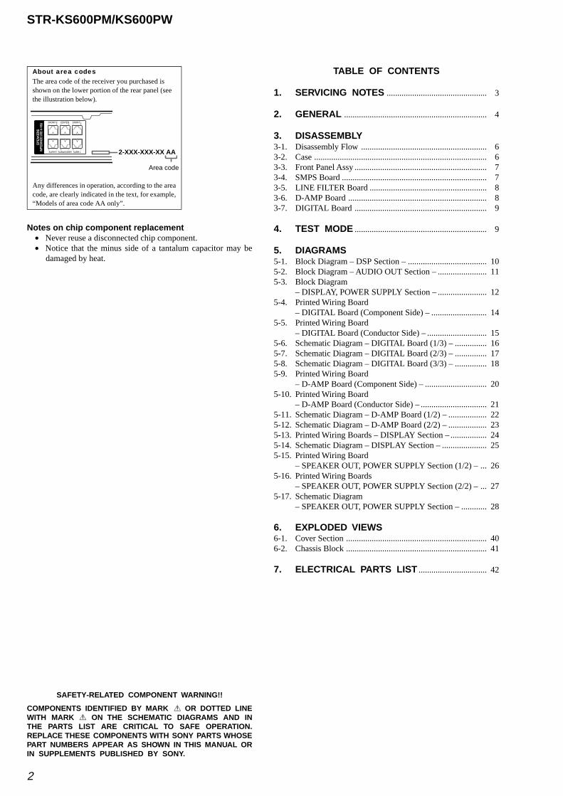
TABLE OF CONTENTS
1. SERVICING NOTES ............................................... 3
2. GENERAL ................................................................... 4
3. DISASSEMBLY3-1. Disassembly Flow ........................................................... 63-2. Case ................................................................................. 63-3. Front Panel Assy .............................................................. 73-4. SMPS Board .................................................................... 73-5. LINE FILTER Board ....................................................... 83-6. D-AMP Board ................................................................. 83-7. DIGITAL Board .............................................................. 9
4. TEST MODE .............................................................. 9
5. DIAGRAMS5-1. Block Diagram – DSP Section – ..................................... 105-2. Block Diagram – AUDIO OUT Section – ....................... 115-3. Block Diagram
– DISPLAY, POWER SUPPLY Section – ....................... 125-4. Printed Wiring Board
– DIGITAL Board (Component Side) – .......................... 145-5. Printed Wiring Board
– DIGITAL Board (Conductor Side) – ............................ 155-6. Schematic Diagram – DIGITAL Board (1/3) – ............... 165-7. Schematic Diagram – DIGITAL Board (2/3) – ............... 175-8. Schematic Diagram – DIGITAL Board (3/3) – ............... 185-9. Printed Wiring Board
– D-AMP Board (Component Side) – ............................. 205-10. Printed Wiring Board
– D-AMP Board (Conductor Side) – ............................... 215-11. Schematic Diagram – D-AMP Board (1/2) – .................. 225-12. Schematic Diagram – D-AMP Board (2/2) – .................. 235-13. Printed Wiring Boards – DISPLAY Section – ................. 245-14. Schematic Diagram – DISPLAY Section – ..................... 255-15. Printed Wiring Board
– SPEAKER OUT, POWER SUPPLY Section (1/2) – ... 265-16. Printed Wiring Boards
– SPEAKER OUT, POWER SUPPLY Section (2/2) – ... 275-17. Schematic Diagram
– SPEAKER OUT, POWER SUPPLY Section – ............ 28
6. EXPLODED VIEWS6-1. Cover Section .................................................................. 406-2. Chassis Block .................................................................. 41
7. ELECTRICAL PARTS LIST ................................ 42
Notes on chip component replacement• Never reuse a disconnected chip component.• Notice that the minus side of a tantalum capacitor may be
damaged by heat.
SAFETY-RELATED COMPONENT WARNING!!
COMPONENTS IDENTIFIED BY MARK 0 OR DOTTED LINEWITH MARK 0 ON THE SCHEMATIC DIAGRAMS AND INTHE PARTS LIST ARE CRITICAL TO SAFE OPERATION.REPLACE THESE COMPONENTS WITH SONY PARTS WHOSEPART NUMBERS APPEAR AS SHOWN IN THIS MANUAL ORIN SUPPLEMENTS PUBLISHED BY SONY.
About area codesThe area code of the receiver you purchased is shown on the lower portion of the rear panel (see the illustration below).
Any differences in operation, according to the area code, are clearly indicated in the text, for example, “Models of area code AA only”.
FRONT R– +
CENTER– +
FRONT L– +
SURR R+ –
SUBWOOFER+ –
SURR L+ – 2-XXX-XXX-XX AA
Area code
3
STR-KS600PM/KS600PWSECTION 1
SERVICING NOTES
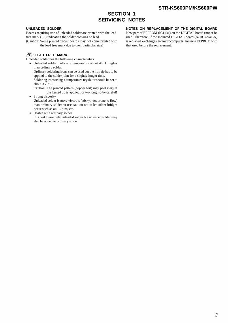
NOTES ON REPLACEMENT OF THE DIGITAL BOARDNew part of EEPROM (IC1131) on the DIGITAL board cannot beused. Therefore, if the mounted DIGITAL board (A-1097-941-A)is replaced, exchange new microcomputer and new EEPROM withthat used before the replacement.
UNLEADED SOLDERBoards requiring use of unleaded solder are printed with the lead-free mark (LF) indicating the solder contains no lead.(Caution: Some printed circuit boards may not come printed with
the lead free mark due to their particular size)
: LEAD FREE MARKUnleaded solder has the following characteristics.
• Unleaded solder melts at a temperature about 40 °C higherthan ordinary solder.Ordinary soldering irons can be used but the iron tip has to beapplied to the solder joint for a slightly longer time.Soldering irons using a temperature regulator should be set toabout 350 °C.Caution: The printed pattern (copper foil) may peel away if
the heated tip is applied for too long, so be careful!• Strong viscosity
Unleaded solder is more viscou-s (sticky, less prone to flow)than ordinary solder so use caution not to let solder bridgesoccur such as on IC pins, etc.
• Usable with ordinary solderIt is best to use only unleaded solder but unleaded solder mayalso be added to ordinary solder.
4
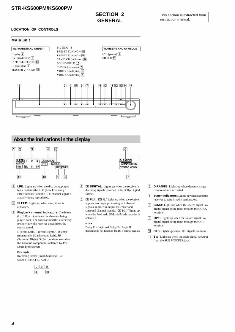
STR-KS600PM/KS600PWSECTION 2GENERAL
This section is extracted frominstruction manual.
LOCATION OF CONTROLS
Main unit
Display 2
DVD (indicator) 5
INPUT SELECTOR qdIR (receptor) 8
MASTER VOLUME qg
MUTING qf
PRESET TUNING + q;
PRESET TUNING – 9
SA-CD/CD (indicator) 6
SOUND FIELD qs
TUNER (indicator) 7
VIDEO 1 (indicator) 3
VIDEO 2 (indicator) 4
?/1 (power) 1
; PLII qa
ALPHABETICAL ORDER NUMBERS AND SYMBOLS
1 2 qd qgqs qfqaq;9876543
A LFE: Lights up when the disc being played back contains the LFE (Low Frequency Effect) channel and the LFE channel signal is actually being reproduced.
B SLEEP: Lights up when sleep timer is activated.
C Playback channel indicators: The letters (L, C, R, etc.) indicate the channels being played back. The boxes around the letters vary to show how the receiver downmixes the source sound.
L (Front Left), R (Front Right), C (Center (monaural)), SL (Surround Left), SR (Surround Right), S (Surround (monaural or the surround components obtained by Pro Logic processing))
Example: Recording format (Front /Surround): 3/2
Sound Field: A.F.D. AUTO
D ; DIGITAL: Lights up when the receiver is decoding signals recorded in the Dolby Digital format.
E ; PLII: “; PL” lights up when the receiver applies Pro Logic processing to 2 channel signals in order to output the center and surround channel signals. “; PLII” lights up when the Pro Logic II Movie/Music decoder is activated.
NoteDolby Pro Logic and Dolby Pro Logic II decoding do not function for DTS format signals.
F D.RANGE: Lights up when dynamic range compression is activated.
G Tuner indicators: Lights up when using the receiver to tune in radio stations, etc.
H COAX: Lights up when the source signal is a digital signal being input through the COAX terminal.
I OPT: Lights up when the source signal is a digital signal being input through the OPT terminal.
J DTS: Lights up when DTS signals are input.
K SW: Lights up when the audio signal is output from the SUB WOOFER jack.
About the indications in the display
L C R
SL S SRSW STEREO MONO
D. RANGEMEMORY
DIGITALSLEEPPL RDSOPT COAX
LFE DTS
78qa q; 9
21 3 4 5 6
L C R
SL SR
5
STR-KS600PM/KS600PW
* The MASTER VOL +, numeric button 5 and H
buttons have a tactile dot. Use the tactile dot as areference when operating the receiver and otheraudio/video components.
Remote buttondescription
1 2 3
4 6
7 8
0/10 ENTER
9
SYSTEM STANDBY
TV/VIDEOSLEEP
TESTTONE
AV?/1
VIDEO 1 VIDEO 2 DVD SA-CD/CD
2CH A.F.D.
RETURN/EXITTV CH –
PRESET –TV CH +
PRESET +
TUNING –
TV
TUNING +
REPLAY ADVANCEc STEP C
DISPLAY
MOVIE MUSIC
MEMORY SHIFT
D.SKIPCLEAR ANGLEAV
MENUTOP MENU/
GUIDE MUTING
TV VOLMASTER VOL
FM MODEMPX
AUDIOD.TUNING
ANT
JUMP
SUBTITLE
DUAL MONO
TUNER MAIN MENU
TV ?/1?/1
>10-
F
G g
f
ENTER
.
Hm M
X x
< < >
5
1
3
2
4ejek
el
eh
8
9
q;qaqs
qf
qd
qj
qh
qk
w;
wa*ws
wd
wf
wh
wj
e;
wg
wk
wl
ea
*es
efeg
ql
qg*
5
67
ed
The tables below show the settings of each button.
Remote Button
Operations Function
A.F.D. ef Receiver Selects the decoding mode for audio sound.
ANGLE qs
DVD player Selects viewing angle or changes the angles.
ANT0 VCR/Satellite tuner
Selects output signal from the antenna terminal: TV signal or VCR program.
AUDIO9
DVD player/Satellite tuner
Changes the sound to Multiplex or Bilingual or Multi channel TV sound.
AVMENU qd
VCR/DVD player/Satellite tuner
Displays menu.
AV ?/1
1VCR/CD player/DVD player/Satellite tuner/MD deck
Turns the audio and video components on or off.
CLEAR ea
DVD player/Satellite tuner
Clears a mistake when you press the incorrect numeric buttons or returns to continuous playback etc.
DISPLAY qh
Receiver/CD player/VCR/DVD player/Satellite tuner/MD deck
Selects information displayed on the TV screen.
D.SKIP qa
CD player/DVD player
Skips discs (multi-disc changer only).
D.TUNING0
Receiver Enters direct tuning mode.
DUALMONO 8
Receiver Selects the language you want during digital broadcast.
DVD3 Receiver To watch DVD.
ENTER qa
TV/VCR/Satellite tuner
After selecting a channel, disc or track using the numeric buttons, press to enter the value.
Remote Button
Operations Function
ENTER wl Receiver/VCR/DVD player/Satellite tuner/CD player/MD deck
Enters the selection.
FM MODE 9
Receiver Selects FM monaural or stereo reception.
JUMP qs Satellite tuner Toggles between the previous and the current channels.
MAIN MENU 5
Receiver Selects the menu of the receiver.
MASTER VOL +/–qg
Receiver/TV Adjusts the master volume of the receiver.
MEMORY qa
Receiver Stores the radio stations.
MOVIE 6 Receiver Selects the pre-programmed sound fields for movie.
MPX 9 VCR Select main or sub language.
MUSIC 7 Receiver Selects the pre-programmed sound fields for music.
MUTING qf Receiver Mutes the sound from the receiver.
PRESET +/– qjwh
Receiver Selects preset stations.
TV/VCR/Satellite tuner
Select preset channel.
RETURN/EXIT wj
DVD player Returns to the previous menu or exits the menu.
Satellite tuner Exits the menu.
SA-CD/CD 4
Receiver To listen to Super Audio CD or compact disc.
SHIFT qs Receiver Selects a memory page for presetting radio stations or tuning to preset stations.
Notes• Some functions explained in this section may not
work depending on the model.
• The above explanation is intended to serve as an example only. Therefore, depending on the component the above operation may not be possible or may operate differently than described.
• When you press input buttons (VIDEO 1, VIDEO 2 or DVD), the input mode of the TV might not switch to the corresponding input mode that you want. In this case, press TV/VIDEO button to switch the input mode of the TV.
• To activate the buttons with orange printing, press TV and the button you want simultaneously.
.
Remote Button
Operations Function
X ws VCR/CD player/DVD player/MD deck/Tape deck
Pauses playback or recording. (Also starts recording with components in recording standby.)
x w; VCR/CD player/DVD player/MD deck/Tape deck
Stops playback.
O wj DVD player Returns to the previous menu or exits the menu.
V/v wk Receiver Selects a menu item.
B/b wk Receiver Adjusts or changes the setting.
V/v/B/b wk VCR/Satellite tuner/DVD player
Selects a menu item.
Remote Button
Operations Function
SLEEP el Receiver Activates the sleep function and the duration which the receiver turns off automatically.
SUBTITLE 0
DVD player Changes the subtitles.
SYSTEM STANDBY (Press AV?/11 and ?/12 at the same time)
Receiver/TV/VCR/CD player/DVD player/Satellite tuner/MD deck
Turns off the receiver and other Sony audio/video components.
TESTTONE ek
Receiver Outputs test tone.
TOP MENU/GUIDE e;
DVD player Displays DVD title.
Satellite tuner Display guide menu.
TUNER eg Receiver To listen to radio programs.
TUNING +/– ql wf
Receiver Scans radio station.
TV wd TV To watch TV programs.
TV CH +/– qj wh
TV Selects preset TV channels.
TV/VIDEO el
TV Selects input signal: TV input or video input.
TV VOL+/– qg
TV Adjusts the volume of the TV.
TV ?/12 TV Turns the TV on or off.
VIDEO 1ej
Receiver To watch VCR.(VTR mode 3)
VIDEO 2eh
Receiver To watch VCR.(VTR mode 1)
Remote Button
Operations Function
1-9 and 0/10 es
Receiver Use with SHIFT to preset radio station or tuning to preset stations and with D.TUNING for direct tuning.
CD player/DVD player/MD deck
Selects track numbers. 0/10 selects track 10.
TV/VCR/Satellite tuner
Selects channel numbers.
2CH ed Receiver Selects 2CH STEREO mode.
>10 ea VCR/CD player/DVD player/Satellite tuner/MD deck
Selects track numbers over 10.
-/-- ea TV Selects the channel entry mode, either one or two digit.
?/12 Receiver Turns the receiver on or off.
c STEP C
REPLAY /ADVANCEwg qk
VCR/DVD player
Replay the previous scene or fast forward the current scene.
./>
wh qjVCR/CD player/DVD player
Skips tracks.
m/M
wf qlDVD player Searches tracks in the
forward or backward direction.
VCR/CD player/MD deck/Tape deck
Fastforwards or rewinds.
H wa VCR/CD player/DVD player/MD deck/Tape deck
Starts playback.
<
<
STR-KS600PM/KS600PW
6
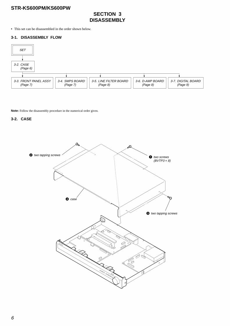
Note: Follow the disassembly procedure in the numerical order given.
3-2. CASE
• This set can be disassembled in the order shown below.
3-1. DISASSEMBLY FLOW
SECTION 3DISASSEMBLY
3 two tapping screws
1 two screws(BVTP3 × 8)
2 two tapping screws
4 case
3-2. CASE(Page 6)
SET
3-3. FRONT PANEL ASSY(Page 7)
3-4. SMPS BOARD(Page 7)
3-5. LINE FILTER BOARD(Page 8)
3-6. D-AMP BOARD(Page 8)
3-7. DIGITAL BOARD(Page 9)
STR-KS600PM/KS600PW
7
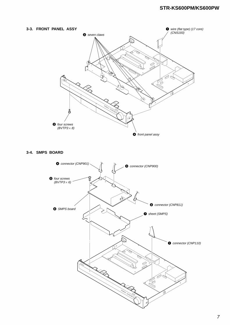
3-3. FRONT PANEL ASSY
3-4. SMPS BOARD
3 seven claws
1 wire (flat type) (17 core)(CNS193)
4 front panel assy
2 four screws(BVTP3 × 8)
1 connector (CNP110)
7 sheet (SMPS)
2 connector (CNP811)
3 connector (CNP900)4 connector (CNP901)
6 SMPS board
5 four screws(BVTP3 × 6)
STR-KS600PM/KS600PW
8
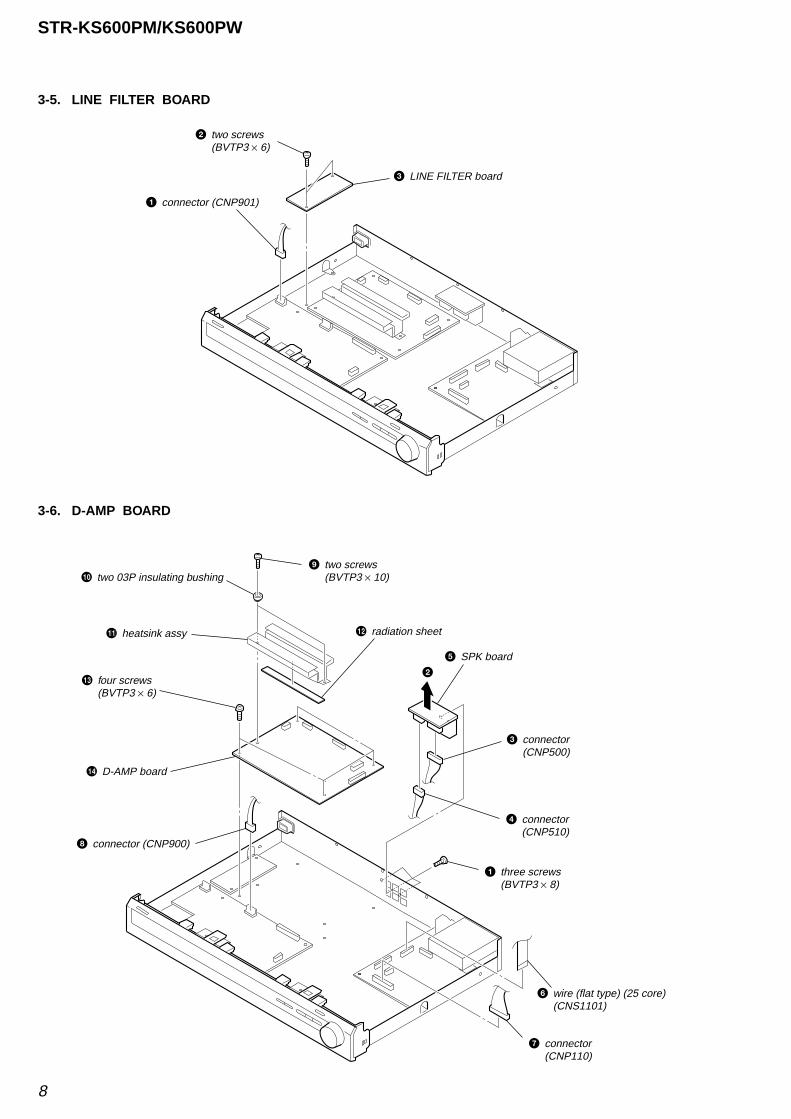
3-5. LINE FILTER BOARD
3-6. D-AMP BOARD
0 two 03P insulating bushing
qa heatsink assy qs radiation sheet
qd four screws(BVTP3 × 6)
qf D-AMP board
5 SPK board
2
3 connector(CNP500)
4 connector(CNP510)
1 three screws(BVTP3 × 8)
6 wire (flat type) (25 core)(CNS1101)
7 connector(CNP110)
9 two screws(BVTP3 × 10)
8 connector (CNP900)
1 connector (CNP901)
3 LINE FILTER board
2 two screws(BVTP3 × 6)
99
STR-KS600PM/KS600PW
STR-KS600PM/KS600PW
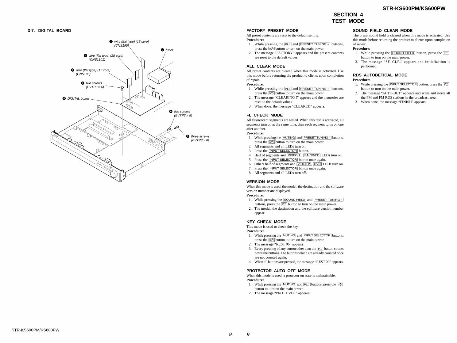
3-7. DIGITAL BOARD
2 three screws(BVTP3 × 8)
6 five screws(BVTP3 × 8)
8 DIGITAL board
7 two screws(BVTP3 × 6)
5 wire (flat type) (17 core)(CNS193)
4 wire (flat type) (25 core)(CNS1101)
1 wire (flat type) (15 core)(CNS195)
3 tuner
SECTION 4TEST MODE
FACTORY PRESET MODEAll preset contents are reset to the default setting.Procedure:
1. While pressing the PLII and [PRESET TUNING +] buttons,press the I/1 button to turn on the main power.
2. The message “FACTORY” appears and the present contentsare reset to the default values.
ALL CLEAR MODEAll preset contents are cleared when this mode is activated. Usethis mode before returning the product to clients upon completionof repair.Procedure:
1. While pressing the PLII and [PRESET TUNING --] buttons,press the I/1 button to turn on the main power.
2. The message “CLEARING !” appears and the memories arereset to the default values.
3. When done, the message “CLEARED” appears.
FL CHECK MODEAll fluorescent segments are tested. When this test is activated, allsegments turn on at the same time, then each segment turns on oneafter another.Procedure:
1. While pressing the [MUTING] and [PRESET TUNING --] buttons,press the I/1 button to turn on the main power.
2. All segments and all LEDs turn on.3. Press the [INPUT SELECTOR] button.4. Half of segments and [VIDEO 1], [SA-CD/CD] LEDs turn on.5. Press the [INPUT SELECTOR] button once again.6. Others half of segments and [VIDEO 2], [DVD] LEDs turn on.7. Press the [INPUT SELECTOR] button once again.8. All segments and all LEDs turn off.
VERSION MODEWhen this mode is used, the model, the destination and the softwareversion number are displayed.Procedure:
1. While pressing the [SOUND FIELD] and [PRESET TUNING --]
buttons, press the I/1 button to turn on the main power.2. The model, the destination and the software version number
appear.
KEY CHECK MODEThis mode is used to check the key.Procedure:
1. While pressing the [MUTING] and [INPUT SELECTOR] buttons,press the I/1 button to turn on the main power.
2. The message “REST 06” appears.3. Every pressing of any button other than the I/1 button counts
down the buttons. The buttons which are already counted onceare not counted again.
4. When all buttons are pressed, the message “REST 00” appears.
PROTECTOR AUTO OFF MODEWhen this mode is used, a protector on state is maintainable.Procedure:
1. While pressing the [MUTING] and PLII buttons, press the I/1
button to turn on the main power.2. The message “PROT EVER” appears.
SOUND FIELD CLEAR MODEThe preset sound field is cleared when this mode is activated. Usethis mode before returning the product to clients upon completionof repair.Procedure:
1. While pressing the [SOUND FIELD] button, press the I/1
button to turn on the main power.2. The message “SF. CLR.” appears and initialization is
performed.
RDS AUTOBETICAL MODEProcedure:
1. While pressing the [INPUT SELECTOR] button, press the I/1
button to turn on the main power.2. The message “AUTO-BET” appears and scans and stores all
the FM and FM RDS stations in the broadcast area.3. When done, the message “FINISH” appears.
1010
STR-KS600PM/KS600PW
STR-KS600PM/KS600PW
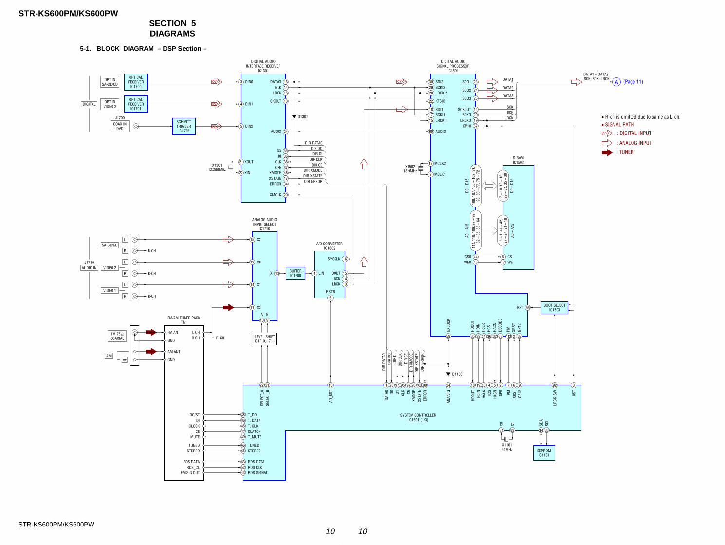
SECTION 5DIAGRAMS
5-1. BLOCK DIAGRAM – DSP Section –
BOOT SELECTIC1503
LEVEL SHIFTQ1710, 1711
BUFFERIC1600
EEPROMIC1131
SYSTEM CONTROLLERIC1601 (1/3)
OPTICALRECEIVER
IC1700
D1103
CS6
10
A
9
B
X215
X012
X1
L CHR CH
DO/STDI
14
X311
LIN1
SDI230BCKI229LRCKI228
KFSIO22
SDI118BCKI117
AUDIO69
LRCKI115
DIN03
D0
98
D1
97
CLK
95
CE
96
ERRO
R
99
ANA/
DIG
24 18 19 20 4 5 2 7 6 9
XMOD
E
93
XSTA
TE
100DA
TA0
1
AD_R
ST
10
SELE
CT_B
21
SELE
CT_A
22
88
EXLO
CK
59
RSTB
6
CS0 44
SDO1 23
SDO2 24
SDO3 25
SCKOUT 14BCKO 20
LRCKO
DATA1DATA1 – DATA3,SCK, BCK, LRCK
DATA2
DATA3
SCKBCK
LRCK19
GP10 67
DOUT 15
SYSCLK 16
BCK 14LRCK 13
X 13
DO 35DI 36
CLK 38CKE 37
ERROR 34
XMODE 48XSTATE
DIR DO
HDOU
T
35
HDIN
33
HCLK
34
HCS
36
HACN
32
DECO
DE
68
PM
113
XRST
2
GP12
37
DIR DATA0
DIR DIDIR CLK
DIR CE
DIR ERROR
DIR XMODEDIR XSTATE
DIR
DODI
R DA
TA0
DIR
DIDI
R CL
KDI
R CE
DIR
ERRO
R
DIR
XMOD
EDI
R XS
TATE
17
XMCLK 20
DATAO 16BLK 14
LRCK 15
CKOUT 13
AUDIO 24
OPT INSA-CD/CD
OPTICALRECEIVER
IC1701DIN14OPT IN
VIDEO 2
SCHMITTTRIGGERIC1702
DIGITAL AUDIOINTERFACE RECEIVER
IC1301
DIGITAL AUDIOSIGNAL PROCESSOR
IC1501
DIN2
J1700
5COAX INDVD
FM 75ΩCOAXIAL
86858789
535243
6665
WE17WE0 45
BST 56
DIGITAL
SA-CD/CD
VIDEO 2AUDIO INJ1710
FM/AM TUNER PACKTN1
VIDEO 1
AM
L
R
L
R
L
R
R-CH
R-CH
R-CH
ANALOG AUDIOINPUT SELECT
IC1710
A/D CONVERTERIC1602
S-RAMIC1502
R-CH
21
22
X130112.288MHz
XOUT
XIN 9
12X1502
13.9MHzMCLK1
MCLK2
FM ANT
GND
AM ANT
GND
CLOCKCE
MUTE
TUNEDSTEREO
RDS DATARDS_CL
FM SIG OUT
T_DOT. DATAT. CLKSLATCHT_MUTE
TUNEDSTEREO
RDS DATARDS CLKRDS SIGNAL
108,
107
, 105
– 1
02, 9
9,98
, 80
– 77
, 75
– 72
7 –
10, 1
3 –
16,
29 –
32,
35
– 38
112,
110
, 109
, 97
– 92
,82
– 8
5, 6
6 –
64
D0 –
D15
A0 –
A15
5 –
1, 4
4 –
42,
27 –
24,
21
– 18
D0 –
D15
A0 –
A15
D1301
HDOU
THD
INHC
LKHC
SHA
CN GP9
PMXR
STGP
12
92
LRCK
_SW
3
BST
82 83
X0 X1
34
SDA
33
SCL
X110124MHz
A
• SIGNAL PATH
: TUNER
: ANALOG INPUT
: DIGITAL INPUT
• R-ch is omitted due to same as L-ch.
(Page 11)
1111
STR-KS600PM/KS600PW
STR-KS600PM/KS600PW
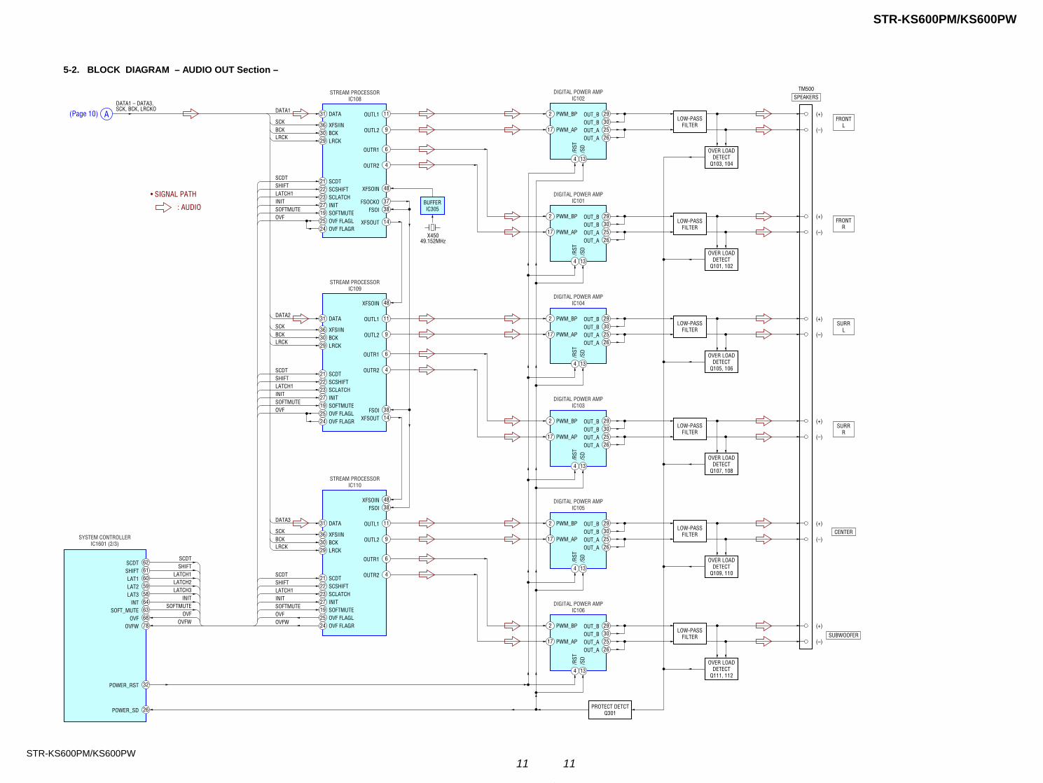
5-2. BLOCK DIAGRAM – AUDIO OUT Section –
• SIGNAL PATH
: AUDIO
/RST
/SD
4 13
DIGITAL POWER AMPIC102
2 PWM_BP
TM500
(+)
(–)
29OUT_B
25OUT_A30OUT_B
26OUT_A
STREAM PROCESSORIC108
31 DATA
36 XFSIIN30 BCK
23 SCLATCH27 INIT19 SOFTMUTE
21 SCDT
29 LRCK
22 SCSHIFTLATCH1INITSOFTMUTE
SCDTSHIFT
6OUTR1
11OUTL1
4OUTR2
17 PWM_AP9OUTL2
38FSOI
OVER LOADDETECT
Q103, 104
LOW-PASSFILTER
FRONTL
FRONTR
SYSTEM CONTROLLERIC1601 (2/3)
37FSOCKO
48XFSOIN
14XFSOUT
SURRL
SURRR
CENTER
SPEAKERS
SUBWOOFER
DATA1
SCKBCKLRCK
INIT
LATCH1LATCH2LATCH3
SCDTSHIFT
BUFFERIC305
DATA1 – DATA3,SCK, BCK, LRCKO
A
X45049.152MHz
62SCDT61SHIFT60LAT159LAT258LAT364INT
SOFTMUTE63SOFT_MUTE
OVF68OVF
OVFW78OVFW
32POWER_RST
26POWER_SD
25 OVF FLAGLOVF
24 OVF FLAGR
STREAM PROCESSORIC109
31 DATA
36 XFSIIN30 BCK
23 SCLATCH27 INIT19 SOFTMUTE
21 SCDT
29 LRCK
22 SCSHIFTLATCH1INITSOFTMUTE
SCDTSHIFT
6OUTR1
11OUTL1
4OUTR2
9OUTL2
38FSOI
48XFSOIN
14XFSOUT
DATA2
SCKBCKLRCK
25 OVF FLAGLOVF
24 OVF FLAGR
STREAM PROCESSORIC110
31 DATA
36 XFSIIN30 BCK
23 SCLATCH27 INIT19 SOFTMUTE
21 SCDT
29 LRCK
22 SCSHIFTLATCH1INITSOFTMUTE
SCDTSHIFT
6OUTR1
11OUTL1
4OUTR2
9OUTL2
38FSOI48XFSOIN
DATA3
SCKBCKLRCK
25 OVF FLAGLOVF
24 OVF FLAGROVFW
/RST
/SD
4 13
DIGITAL POWER AMPIC101
2 PWM_BP (+)
(–)
29OUT_B
25OUT_A30OUT_B
26OUT_A17 PWM_AP
OVER LOADDETECT
Q101, 102
LOW-PASSFILTER
/RST
/SD
4 13
DIGITAL POWER AMPIC104
2 PWM_BP (+)
(–)
29OUT_B
25OUT_A30OUT_B
26OUT_A17 PWM_AP
OVER LOADDETECT
Q105, 106
LOW-PASSFILTER
/RST
/SD
4 13
DIGITAL POWER AMPIC103
2 PWM_BP (+)
(–)
29OUT_B
25OUT_A30OUT_B
26OUT_A17 PWM_AP
OVER LOADDETECT
Q107, 108
LOW-PASSFILTER
/RST
/SD
4 13
DIGITAL POWER AMPIC105
2 PWM_BP (+)
(–)
29OUT_B
25OUT_A30OUT_B
26OUT_A17 PWM_AP
OVER LOADDETECT
Q109, 110
LOW-PASSFILTER
/RST
/SD
4 13
DIGITAL POWER AMPIC106
2 PWM_BP (+)
(–)
29OUT_B
25OUT_A30OUT_B
26OUT_A17 PWM_AP
OVER LOADDETECT
Q111, 112
LOW-PASSFILTER
PROTECT DETCTQ301
(Page 10)
1212
STR-KS600PM/KS600PW
STR-KS600PM/KS600PW
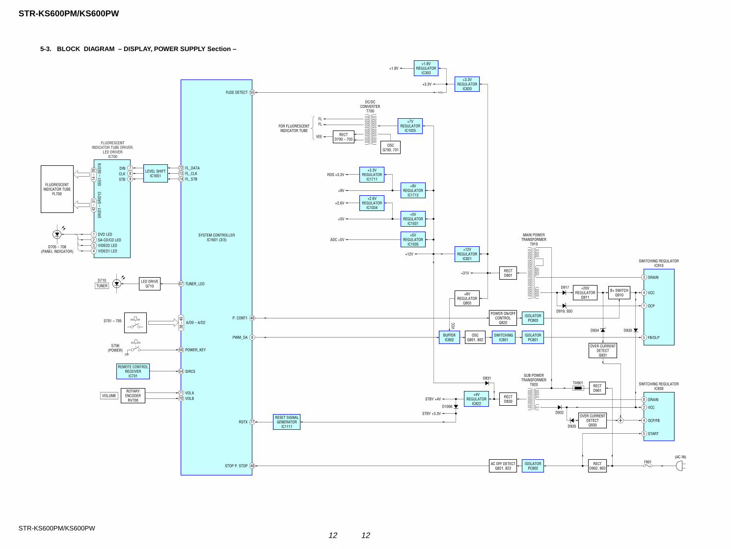
5-3. BLOCK DIAGRAM – DISPLAY, POWER SUPPLY Section –
3
SWITCHING REGULATORIC910
DRAIN
(AC IN)
MAIN POWERTRANSFORMER
T910
SUB POWERTRANSFORMER
T920
F901
VCC
D917
RECTD902, 903
ISOLATORPC801
OSCQ801, 802
B+ SWITCHQ910
BUFFERIC802
4 VCC
1 OCP
5 FB/OLP
8
SWITCHING REGULATORIC930
DRAIN
2 VCC
4 OCP/FB
5 START
RECTD801
RECTD830
ISOLATORPC803
ISOLATORPC802
SWITCHINGIC801
D932
D935
D831
D1006
STBY +4V
D930
+20VREGULATOR
Q911
OVER CURRENTDETECT
Q930
OVER CURRENTDETECT
Q931
AC OFF DETECTQ821, 822
POWER ON/OFFCONTROL
Q820
+6VREGULATOR
Q803
+31V
STBY +3.3V
+4VREGULATOR
IC822
RESET SIGNALGENERATOR
IC1111
48STOP P. STOP
77RSTX
8PWM_DA
46P. CONT1
55FUSE DETECT
SYSTEM CONTROLLERIC1601 (3/3)
RECTD901
+
D934
D919, 920
TH901
+12V+12V
REGULATORIC821
+7VREGULATOR
IC1025
+3.3V+3.3V
REGULATORIC820
ADC +5V+5V
REGULATORIC1035
+2.6V+2.6V
REGULATORIC1034
+5V+5V
REGULATORIC1031
RDS +3.3V+3.3V
REGULATORIC1711
+1.8V+1.8V
REGULATORIC303
+9V+9V
REGULATORIC1712
FLFL
VEE
FOR FLUORESCENTINDICATOR TUBE
DC/DCCONVERTER
T700
RECTD700 – 703
OSCQ700, 701
72 FL_DATA73 FL_CLK74 FL_STB
FLUORESCENTINDICATOR TUBE DRIVER,
LED DRIVERIC700
7DIN8CLK9STB
1 DVD LED2 SA-CD/CD LED3 VIDEO2 LED4 VIDEO1 LED
D705 – 708(PANEL INDICATOR)
FLUORESCENTINDICATOR TUBE
FL700
SEG1
– S
EG16
14 –
29
GRID
1 –
GRID
1242
– 3
1
54 SIRCS
ROTARYENCODER
RV700
LEVEL SHIFTIC1651
REMOTE CONTROLRECEIVER
IC701
VOLUME
38 –
40
A/D0 – A/D2S701 – 705
56 POWER_KEY
70 VOLB71 VOLA
67 TUNER_LEDD710 LED DRIVE
Q710TUNER
S706(POWER)
1313
STR-KS600PM/KS600PW
STR-KS600PM/KS600PW
• Note for Printed Wiring Boards and Schematic Diagrams
Note on Printed Wiring Board:• X : parts extracted from the component side.• Y : parts extracted from the conductor side.• x : parts mounted on the conductor side.• f : internal component.• : Pattern from the side which enables seeing.(The other layers' patterns are not indicated.)• Indication of transistor
Caution:Pattern face side: Parts on the pattern face side seen from(Conductor Side) the pattern face are indicated.Parts face side: Parts on the parts face side seen from(Component Side) the parts face are indicated.
Note on Schematic Diagram:• All capacitors are in µF unless otherwise noted. (p: pF)
50 WV or less are not indicated except for electrolyticsand tantalums.
• All resistors are in Ω and 1/4 W or less unless otherwise
specified.• f : internal component.• 2 : nonflammable resistor.• 5 : fusible resistor.• C : panel designation.
• A : B+ Line.• B : B– Line.• Voltages and waveforms are dc with respect to ground
under no-signal (detuned) conditions.no mark : TUNER
• Voltages are taken with a VOM (Input impedance 10 MΩ).Voltage variations may be noted due to normal produc-tion tolerances.
• Waveforms are taken with a oscilloscope.Voltage variations may be noted due to normal produc-tion tolerances.
• Circled numbers refer to waveforms.• Signal path.J : DIGITAL INPUTF : ANALOG INPUTf : TUNER
Note: The components identified by mark 0 or dotted linewith mark 0 are critical for safety.Replace only with part number specified.
C
B
These are omitted.
E
Q
B
These are omitted.
C E
Q
• Circuit Boards Location
DIGITAL board
VOLUME board
DISPLAY board
SMPS board
LINE FILTER board D-AMP board
SPK board
1414
STR-KS600PM/KS600PW
STR-KS600PM/KS600PW
R1120
X1101
R1166
IC1301
IC1502
IC1501IC1601
R1089
IC1651
R1362C1301C1302
R1301
R1302
R1303
R1304C1303
C1304
C1305
R1606
R1074
L1604
R1076
X1301
R1087
R1523R1515
C1521C1522
R1261
R1502
R1503
R1504
R1505R1506
FB1503
R1073
R1151
R1305
R1311
R1360
R1306
R1307
R1178
R1170
R1171R1172R1173
R1174
R1190
R1183
R1159
R1124
R1129
R1105
R1186
R1122R1123
R1119
R1126
R1125
R1180
R1053
R1056
R1529
R1308
R1309
D1301
R1312
R1313
R1315
R1316
R1136
R1137
R1134
R1135
R1041
R1140
R1142R1143
R1144
IC1503
IC1034
R1160R1161R1162
R1121R1150
R1501
R1149
IC1131R1158
R1071
R1072
R1508
R1509
R1511
R1078
C1299R1541
R1555
R1168
R1548R1549R1550
R1551
R1552R1553R1554
R1525R1526
R1518R1519
R1520R1521R1522
R1517
R1547
R1532R1533
R1534R1535
R1536R1537 R1538 R1539 R1540
R1542 R1543R1544
R1527 R1528
R1184
FB1305
IC1111
IC1602
R1127R1189
C1107
C1137
R1128
R1604
R1260
FB1102
FB1302
FB1312
D1103
R1185R1187
FB1502
R1188
R1167
FB1101
R1182
R1181
R1192R1191
R1195
R1058
R1059
R1169
R1113
R1070
R1115
FB1501C1033
IC1600
C1603
R1251
C1108
R1079
C1602
R1653
C1601R1652
C1652R1654
R1602
C1651
R1603
R1201
R1651
C1441R1601
R1179
R1607
C1443
FB1511
R1044
C1483
FB1301
R1088
R1252
FB1308
R1175
R1608
X1502
IC1702D1700
JR1101
JR1102
FB1700 FB1701
Q1710Q1711
C1700C1701
C1707 C1708
C1723
R1700
R1701
R1702
R1703
R1704
R1705
R1706 R1707
R1728R1729R1730
R1731
R1732
R1733
FB1702 FB1703 FB1704 FB1705
R1708 R1709 R1710 R1711
IC1710
D1001
L1600
C1705
31
30
1
30 1
112
36
37
48
24
13
25
61 90
91
120
60
31
51
80
50
10081
1-864-851-
11
(11)
DIGITAL BOARD (COMPONENT SIDE)
EE
1
3
5
4
13
2
A
B
C
D
E
F
G
1 2 3 4 5
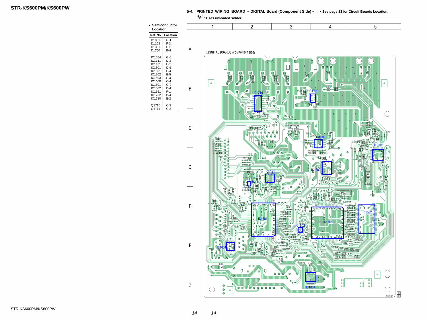
5-4. PRINTED WIRING BOARD – DIGITAL Board (Component Side) – • See page 13 for Circuit Boards Location.
: Uses unleaded solder.
D1001 G-1D1103 F-3D1301 D-5D1700 B-4
IC1034 G-3IC1111 D-2IC1131 D-2IC1301 D-5IC1501 E-4IC1502 E-5IC1503 F-3IC1600 C-4IC1601 G-2IC1602 D-4IC1651 F-1IC1702 B-4IC1710 B-2
Q1710 C-3Q1711 C-3
• SemiconductorLocation
Ref. No. Location
1515
STR-KS600PM/KS600PW
STR-KS600PM/KS600PW
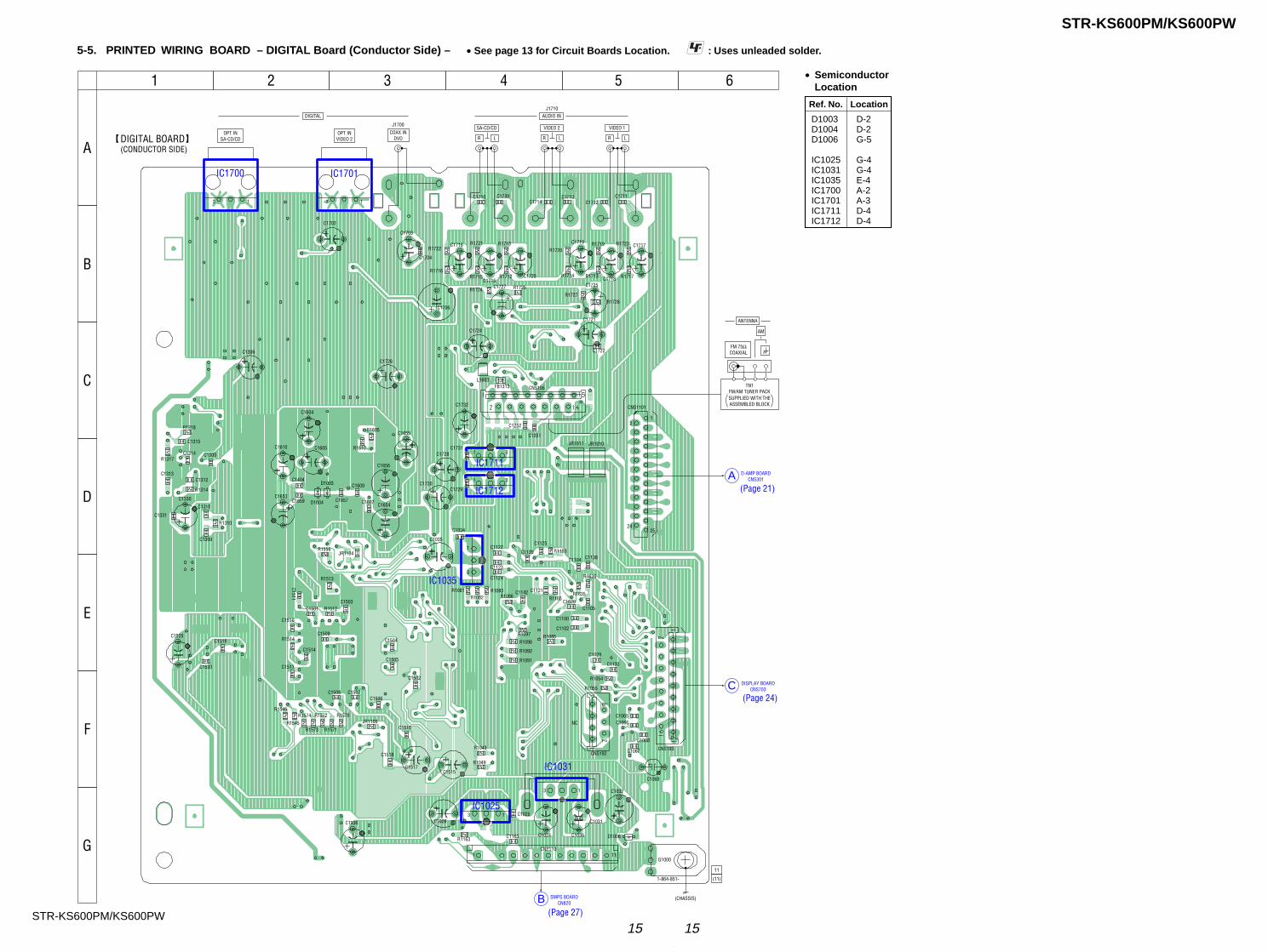
5-5. PRINTED WIRING BOARD – DIGITAL Board (Conductor Side) – • See page 13 for Circuit Boards Location. : Uses unleaded solder.
CNS195
CNS193
C1306
C1069
CNS192
C1525
C1515
C1032
C1656
IC1025
IC1035
C1036C1024
C1026
C1035
C1936
C1605
C1655
C1610
C1653
C1604
C1654
CNP110
G1000
CNS1101
C1330
IC1031
IC1700 IC1701
IC1711
IC1712
J1700
J1710
C1702
C1703
C1706
C1716
C1721
C1724
C1725
C1726
C1727
C1728
C1730
C1732
C1717
C1718C1715C1720
C1719
C1517
C1504
R1091
R1092
C1607
C1138
C1502
R1049
C1505
R1096
R1097
R1086R1082
R1085
R1083
R1570
R1081 C1142 C1121
C1122R1193
C1123
C1124
C1125
C1105
R1636
C1104
R1546
R1545
R1556
C1620
R1635
C1657
R1314
C1310
C1309
C1308
C1312C1313
C1314
C1315
R1317
R1318
C1609
C1067
C1031
R1513
R1571
R1572
R1573
R1574
C1508 C1507C1506
C1503C1501
C1509
C1510
R1514
C1511
R1512
C1513
C1514
C1519
C1520
C1516
C1518
C1066
C1100
C1068
C1025
C1034
R1163 C1163
C1252
C1102
C1129
C1130
R1054
R1055
C1065
C1251
R1610
C1659
C1404
R1043
R1605
D1003
FB1313
D1004
R1165
C1139
D1006
R1310
C1331
L1603
JR1010JR1011
JR1104
C1704
C1709C1710
C1722
C1729
C1731
R1715R1716
R1721R1722
R1724 R1725
R1726R1727
C1711C1712
C1713C1714
R1717
R1723
R1713
R1720R1719
R1714R1712
R1718
JR1106
1
3
DIGITAL BOARD (CONDUCTOR SIDE)
21
2425
1-864-851-
11
(11)
(CHASSIS)
TN1FM/AM TUNER PACKSUPPLIED WITH THEASSEMBLED BLOCK
FM 75ΩCOAXIAL
ANTENNA
AM
DISPLAY BOARDCNS703C
SMPS BOARDCN820B
D-AMP BOARDCNS301A
NC
13
1
1 11
3
VIDEO 1
AUDIO IN
LR
VIDEO 2
LR
SA-CD/CDCOAX IN
DVDOPT IN
VIDEO 2OPT IN
SA-CD/CD LR
DIGITAL
1313
1 3
1 3
A
B
C
D
E
F
G
1 2 3 4 5 6
D1003 D-2D1004 D-2D1006 G-5
IC1025 G-4IC1031 G-4IC1035 E-4IC1700 A-2IC1701 A-3IC1711 D-4IC1712 D-4
• SemiconductorLocation
Ref. No. Location
(Page 21)
(Page 24)
(Page 27)
1616
STR-KS600PM/KS600PW
STR-KS600PM/KS600PW
R1307
R1309
R1312
R1313
R1315
R1306
R1606
R1607
R1651
C1601
R1705R
1712
R1713
R1714
R1715
R1716
R1717
R1718
R1719
R1720
R1721
R1722
R1723
C1725
R1729
FB1511
FB1313
FB1305
C1700
C1701
C1703
R1702
R1703
C1705
IC1702
C1708
R1704
C1707 C1706
C1702
D1700
FB1308
R1362
R1700
C1301
C1305
C1306
R1301
R1302
R1304
C1304
C1303
R1303
C1302
R1314
C1331 C1330
C1308
R1360
C1309
C1310
FB1301
R1308
D1301
R1305
C1603
C1609
R1605C1604
C1653
C1659
R1603
C1656
C1654
R1653
IC1602
C1655
C1607
C1657
C1651
R1602
R1604
R1601
C1035
R1610
C1034
IC1600
R1311
FB1302
C1704
R1706
R1707
R1708
R1709
R1710
R1711FB1705
FB1704
FB1703
FB1702
FB1701
FB1700C1715
C1720
C1719
C1718
C1717
C1716
Q1711
C1252
R1261
R1260
C1732 C1731
IC1711
C1728 C1729
FB1312
C1251
C1441
R1727
D1003
D1004
CNS195
R1251
R1252
C1730
IC1301
R1701
R1652 R1654C1652
C1605
C1602
C1724
R1310
X1301
C1315
R1
318
R1317
R1316
C1313
C1312
C1314
C1404
C1610
R1608
C1443
C1483
R1151
R1731
R1733
C1727
Q1710
R1728
R1732R1730R1726
C1726
C1723
R1725C1721
R1724
C1722
C1709
C1710
C1711
C1712
C1713
C1714
IC1712
JR1101
JR1102
IC1035
IC1710
J1710
IC1700
IC1701
J1700
100
100
100
100
100
22
100
1k
10k
220p
10010k
10k
10k
10k
10k
10k
10k
10k
10k
10k
10k
10k
10 50V
100
0.1
0.1
2250V
1k
22k
1p
TC7WU04F
47p
560k
0.1 10006.3V
1050V
1SS355TE-17 100
100
0.1
0.1
47 16V
5.6k
4.7k
100
0.01
0.1
33k
0.01
10k
0.1 1050V
0.1
100
18p
18p
100
1S
S355TE-1
7
470
0.1
0.1
4.7k
L160310µH
10016V
1050V0.1
3.3k
47 50V
47 50V
3.3k
PCM1800
1050V
0.1
0.1
220p
470
1k
10k
47010V
4.7k
0.1
NJM4565M(TE2)
100
0.1
1k
1k
1k
1k
1k
1k
10 50V
10 50V
10 50V
10 50V
10 50V
10 50V
DTC124EKA-T146
0.1
0
0
4716V 0.1
TA78033LS
4716V
0.1
0.1
0.0033
10k
ISS367-T3
ISS367-T3
15P
39k
39k
1050V
LC89056W
75
10k 10k220p
1050V
220p
10016V
1M
12.2
88M
Hz
0.1
10k
10k
100
100p
0.1
0.1
0.1
L160410µH
4716V
2.2k
470p
470p
100
10k
10k
1050V
DTC124EKA-T146
100
10k10k10k
10016V
0.1
10k10016V
10k
0.1
100p
100p
100p
100p
100p
100p
TA7809
0
0
TA7805LS
MC14052 BDR2
TORX141
TORX141
A1
A2
A3
A4
A5
A6
A8
A9
A10
A12
B1
B2
B8
B3
B4
B5
B6
B7
A13
A11
DA
TA
O
XS
TA
TE
CE
DI
DO
CLK
XMODE
T_M
UTE
LA
T
TD
A
TD
O
TC
LK
RDS DATA
RDS_CL
FM SIG OUT
RDS(3.3V)
MUTE
R CH
GND
L CH
TUNED
VDD 10V
CE
DI
DO/ST
CLOCK
STEREO
+3.3V REGULATOR
+9V REGULATOR
O IG
O IG
A/D CONVERTER
DIGITAL AUDIO
INTERFACE RECEIVER
BUFFER
G
V
OI G
+5V REGULATOR
V
G
SCHMITT TRIGGER
ANALOG AUDIO
INPUT SELECT
LEVEL SHIFT
LEVEL SHIFT
(CHASSIS)
L
R
L
R
L
R
SA-CD/CD
VIDEO 2
VIDEO 1
AUDIO IN
(CHASSIS)
COAX IN
DVD
(1/3)
OPTICAL RECEIVER
OPTICAL RECEIVER
OPT IN
SA-CD/CD
OPT IN
VIDEO 2
DIGITAL
AM
COAXIAL
FM 75Ω
THE ASSEMBLED
BLOCK
SUPPLIED WITH
FM/AM
TUNER PACK
TN1
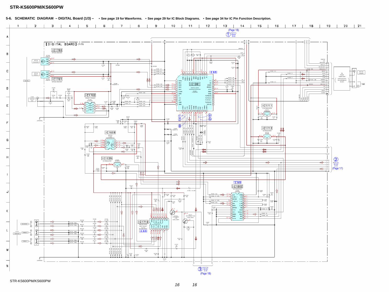
• See page 19 for Waveforms. • See page 29 for IC Block Diagrams. • See page 34 for IC Pin Function Description.5-6. SCHEMATIC DIAGRAM – DIGITAL Board (1/3) –
(Page 18)
(Page 17)
(Page 18)
1717
STR-KS600PM/KS600PW
STR-KS600PM/KS600PW
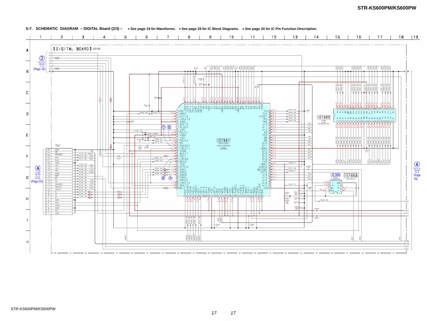
• See page 19 for Waveforms. • See page 29 for IC Block Diagrams. • See page 34 for IC Pin Function Description.5-7. SCHEMATIC DIAGRAM – DIGITAL Board (2/3) –
R1532
R1533
R1545
R1546
R1548
R1549
R1550
R1551
R1502
R1191
R1192
R1195
R1181
R1182
R1183
R1184
R1185
R1187
R1188
R1171
R1172
R1173
R1170
R1166
R1174
JR1106
C1507
R1520
R1521
R1522
R1518
R1519
R1517
R1554
R1553
R1552
R1525
R1526
C1519
R1534
R1547
R1541
R1535
R1536
R1537
R1538
R1539
R1540
R1542
R1543
R1555
R1544
R1527
R1528
R1514
C1510
C1514
C1506
R1570
R1571
R1572
R1573
R1574
R1508
R1161
R1160
R1509
R1121
C1504 C1505
R1506
R1505
R1504
R1503
R1523
R1513
C1522
X1502
R1515
C1521
R1501 C1511
C1501
R1512
R1511
R1142
C1520
FB1501
FB1502
C1516
C1515
C1502
C1518
C1525
C1517
C1509
R1150
C1503
FB1503R1556
CNS1101
IC1502
IC1503
R1120
R1529
C1508
C1513
JR1104
IC1501
220
220
220
220
220
220
220
220
100
100
100
100
100
100
100
100
100
100
100
100
100
100
100
100
100
0
0.1
220
220
220
220
220
220
220
220
220
220
220
0.1
220
220
220
220
220
220
220
220
220
220
220
220
220
220
220
10k
0.1
0.1
0.1
10k
10k
10k
10k
10k
100
100
100
100
100
0.1 0.1
100
100
100
220
220
10k
10p
13.9MHz
1M
10p
100 0.1
0.1
1k
100 100
0.1
0.1
47010V
0.1
0.1
10016V
47010V
0.1
100
0.1
100
25P
IS61LV6416-10TLT
TC7WH157FU
100
220
0.1
0.1
0
CXD9720BQ
B8
B1
B2
B3
B4
B5
B6
B7
C1
C2
C3
C4
C5
C6
C7
C8
C9
INT
SMUTE
SCDT
SHIFT
HD
OU
T
GP
12
PM
XR
ST
HA
CN
HC
S
BS
T
GP
9
A7
A8
A13
A14
A15
A7
A8
A9
A1
0
A1
1
A1
2
A1
3
A1
4
A1
5
D8
D9
D1
0
D1
1
D1
2
D1
3
D1
4
D1
5
A10
A11
A12
A9
D8
D9
D10
D11
D12
D13
D14
D15
A0
A0
A1
A1
A2
A2
D0
D0
D1
D1
D2
D2
D3
D3
D4
D4
D5
D5
D6
D6
D7
D7
A3
A3
A4
A4
A5
A5
A6
CS
0
CS
0
WE
0
WE
0
A6
LAT1
LAT2
LAT3
OVFW
OVF
FON
FCTL
FCLK
HC
LK
HD
IN
D1
D2
D3
BCKO
LRCKO
DGND
SCDT
SHIFT
DGND
LAT1
LAT2
LAT3
INIT
REST
SD
DGND
SOFT MUTE
OVF
SCK
FAN-CLK
FAN ON/OFF
FAN-CTRL
DGND
OVFW
DGND
(2/3)
S-RAM
DIGITAL AUDIO
SIGNAL PROCESSOR
BOOT SELECT
(Page 16)
(Page 23)
(Page18)
1818
STR-KS600PM/KS600PW
STR-KS600PM/KS600PW
R1201
R1122
R1124
R1167
R1168
R1119
R1125
R1126
R1081
R1082
R1086
R1087
R1076
R1092
R1091
R1096
R1115
R1113
R1078
R1079
R1089
R1074
R1053
FB1102
C1123
C1124
C1031
R1137
R1070
R1083
R1193
C1125
C1121
R1165
C1104 C1620
R1071C1142 R1072
R1085
R1169
R1123
R1055
R1056
R1054R1636
C1105
C1100
C1102
C1122
IC1131
R1128
C1065
C1066
C1138
R1189
R1043
R1136
R1135
R1134
R1140
R1041
R1149
R1144
R1143
R1044
FB1101
R1179R1088
R1180
C1067
C1025
R1190
C1033C1936
C1036 C1032
R1163
C1024
IC1025
C1026
C1108
C1137
D1006
D1001CNP110
R1049
R1097
C1069
R1158
R1159
C1163
R1073
CNS192
CNS193
C1068
R1635
R1186
R1105
R1129
R1175
R1059
R1058
C1130
C1129
C1107
C1299
R1178 D1103
R1162
C1139
IC1034 IC1031
IC1111
X1101
IC1601
G1000
IC1651
R1127
22k
100
100
100
100
1k
1k
1k
10k
10k
10k
100
100
10k
10k
10k
100
100
10k
10k
10k
10k
100
0.1
0.1
0.1
100
10k
10k
0
0.1
0.1
0
0.1 0.1
10k0.1 10k
10k
100
100
10k
10k
10k2.2k
0.1
0.1
0.1
0.1
BR24L16F-WE2
100
220p
220p
0.1
10k
10k
100
100
100
100
100
100
100
100
100
10k10k
10k
220p
0.1
10k
0.14750V 10
50V47010V
4.7
k
1050V
TA7807
4716V
0.1
0.01
1SS355TE-17
EC10QS0411P
10k
100k
1050V
3.3k
3.3k
0.1
10k
7P
17PL160010µH
0.12.2k
10k
10k
100
100
220
220
0.01
0.01
0.1
0.1
10k 1SS355TE-17
100
0.1
NLM2391DL1-26 TA7805LS
S-80929CNMC
24MHz
MB90488BPF-G-111E1
TC74VHCT08AFT
100
A1
A2
A3
A4
A5
A6
A8
A9
A10
A11
A12
A13
C1
C2
C3
C4
C5
C7
C6
C8
C9
LA
T3
LA
T2
LA
T1
SH
IFT
SC
DT
SM
UT
E
INT
FC
LK
FO
N
FC
TL
OV
F
TDA
TCLK
OV
FW
HC
LK
HD
IN
HD
OU
T
GP
12
PM
XR
ST
HA
CN
HC
S
BS
T
GP
9
MD
2
MD2
MD0
MD0
DIN
DIN
CLK
CLK
ST
B
STB
DATAO
DO
DI
CE
CLK
XMODE
XSTATE
LAT
TDO
T_MUTE
VOL_JOG(2A)
VOL_JOG(2B)
FL_LAT
FL_DIN
FL_CLK
GND
+3.3V(STBY)
AD2
AD1
AD0
+5V
GND
P_CONT1
STOP
STBY_4V
GND
GND
GND
GND
GND
POWER SW
SIRCS
GND
PWM-DA
+6.5V
TUNER_LED
FLASH1
FLASH2
VDD
GND
RESET
MD0
MD2
DA
TA
O
GP
9
BS
T
HC
S
HA
CN
XR
ST
PM
VS
S
HD
OU
T
HD
IN
HC
LK
VC
C5
AN
A/D
IG
AVCC
AVRH
AVSS
A/D0
A/D1
A/D2
VSS
VERSION
MD0
MD1
MD
2
SIR
CS
PO
WER
KEY
TU
NED
RS
TX
X1A
X0A
VS
S
X0
X1
VCC3
XMODE
CLK
CE
ERROR
XSTATE
CKSEL1
MODEL
FU
SE D
ETEC
T
SDA
SCL
WO
OFER
RELA
Y
FA
N_O
N
FA
N_C
LK
FLA
SH
1R
DS
DA
TA
RD
S C
LK
RDS SIGNAL
XS
CEN
XRST
GP
12
AD
_R
ST
157_C
TL1
157_C
TL2
14052_C
TL1
PO
WER
_S
D
NC
POWER_RST
P.CONT1
LA
T3
LA
T2
LA
T1
SH
IFT
SC
DT
SO
FT_M
UTE
INT
VO
LA
VO
LB
FL_C
LK
FL_S
TB
SLATCH
T_DO
VID
EO
-SW
1
VID
EO
-SW
2
VID
EO
-MU
TE
LRCK_SW
TC74AC_A
TC74AC_B
NO
US
E
FA
N_C
TL
OV
F
PW
M_D
A
T.CLK
T.DATA
A/D3
FLA
SH
2
T_MUTE
SELEC
T_A
SELEC
T_B
TU
NER
_LED
(3/3)
+2.6V REGULATOR +5V REGULATOR
I OG I OG I OG
+7V REGULATOR
RESET SIGNAL
GENARATOR
O V G
NCCD
STER
EO
D1
D0
SYSTEM CONTROLLER
EEPROM
+12V
(CHASSIS)
LEVEL SHIFT
V
G
+3.3V
NC
SMPS RST
STOP P.STOP
FL_D
ATA
OV
FW
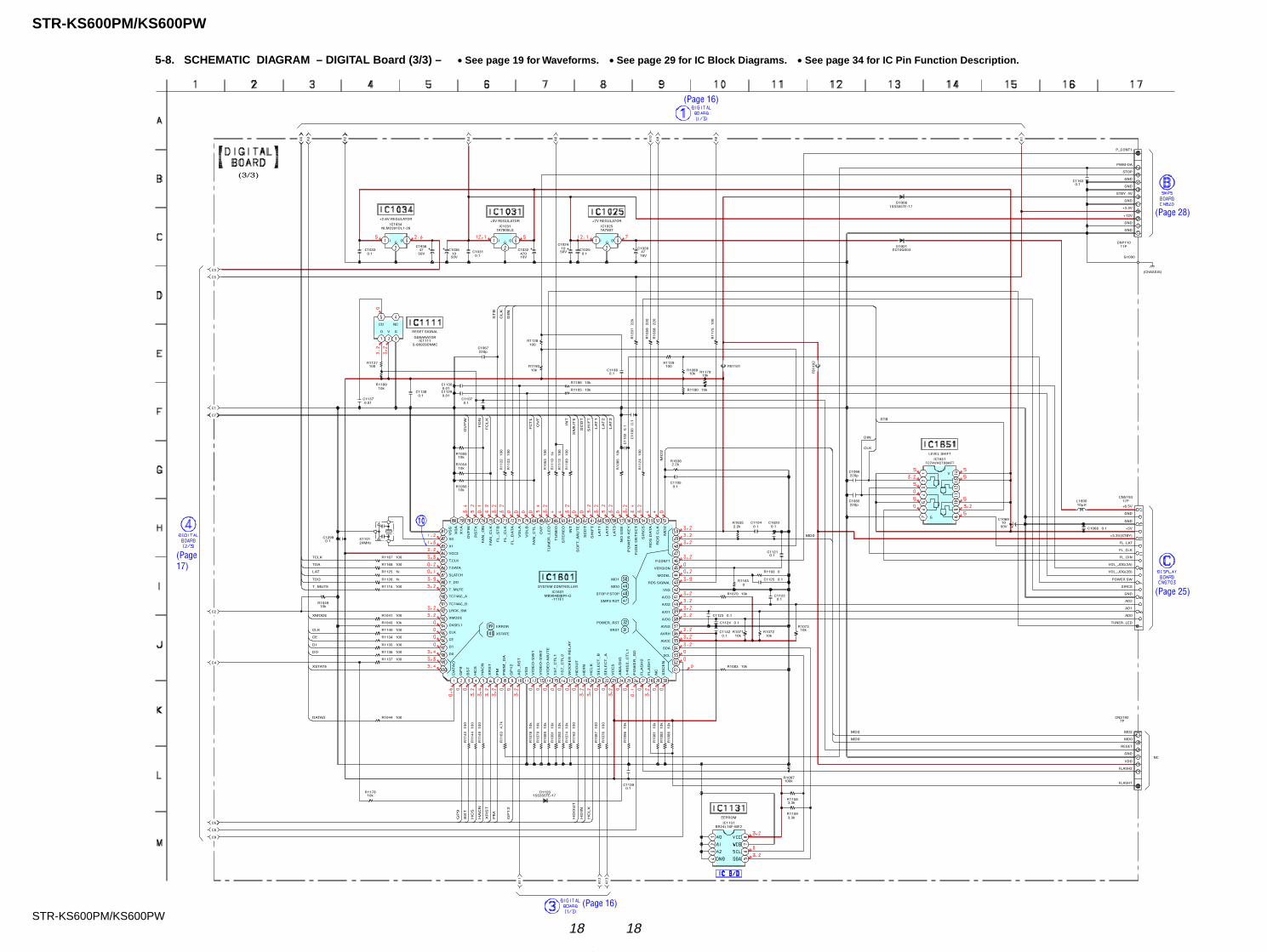
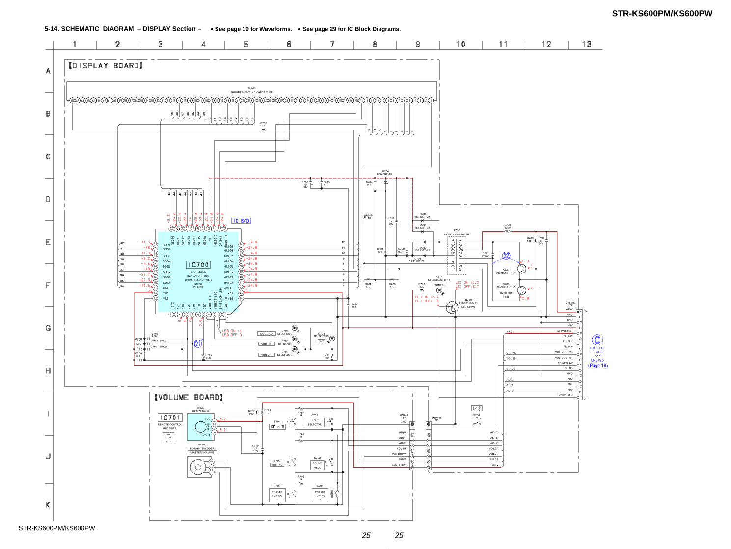
• See page 19 for Waveforms. • See page 29 for IC Block Diagrams. • See page 34 for IC Pin Function Description.5-8. SCHEMATIC DIAGRAM – DIGITAL Board (3/3) –
(Page17)
(Page 16)
(Page 28)
(Page 25)
(Page 16)
1919
STR-KS600PM/KS600PW
STR-KS600PM/KS600PW
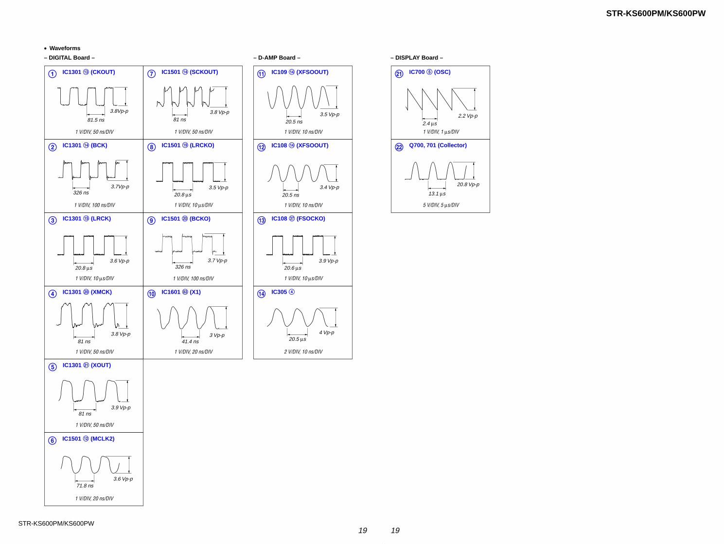
• Waveforms
– D-AMP Board –– DIGITAL Board – – DISPLAY Board –
1 IC1301 qd (CKOUT)
1 V/DIV, 50 ns/DIV
81.5 ns
3.8Vp-p
2 IC1301 qf (BCK)
1 V/DIV, 100 ns/DIV
326 ns3.7Vp-p
20.8 µs3.6 Vp-p
3 IC1301 qg (LRCK)
1 V/DIV, 10 µs/DIV
4 IC1301 w; (XMCK)
1 V/DIV, 50 ns/DIV
81 ns3.8 Vp-p
5 IC1301 wa (XOUT)
1 V/DIV, 50 ns/DIV
81 ns3.9 Vp-p
6 IC1501 qs (MCLK2)
1 V/DIV, 20 ns/DIV
71.8 ns3.6 Vp-p
7 IC1501 qf (SCKOUT)
1 V/DIV, 50 ns/DIV
81 ns3.8 Vp-p
20.8 µs3.5 Vp-p
8 IC1501 ql (LRCKO)
1 V/DIV, 10 µs/DIV
9 IC1501 w; (BCKO)
1 V/DIV, 100 ns/DIV
326 ns3.7 Vp-p
q; IC1601 id (X1)
1 V/DIV, 20 ns/DIV
41.4 ns3 Vp-p
qs IC108 qf (XFSOOUT)
1 V/DIV, 10 ns/DIV
20.5 ns
3.4 Vp-p
20.6 µs3.9 Vp-p
qd IC108 ej (FSOCKO)
1 V/DIV, 10 µs/DIV
qa IC109 qf (XFSOOUT)
1 V/DIV, 10 ns/DIV
20.5 ns3.5 Vp-p
qf IC305 4
2 V/DIV, 10 ns/DIV
20.5 µs4 Vp-p
wa IC700 5 (OSC)
1 V/DIV, 1 µs/DIV
2.4 µs
2.2 Vp-p
ws Q700, 701 (Collector)
5 V/DIV, 5 µs/DIV
13.1 µs
20.8 Vp-p

2020
STR-KS600PM/KS600PW
STR-KS600PM/KS600PW
5-9. PRINTED WIRING BOARD – D-AMP Board (Component Side) – • See page 13 for Circuit Boards Location. : Uses unleaded solder.
C178
R119
Q110
C161
R196
C208
R206
C385
IC102
C201C271
R205
C176 C175C166R191
IC106
C272
R195 R204
C209
C165
R395
C188
IC105
C207 R400C206
R194 R203
C210
C174 C164
IC104
Q112 Q108
C163
C202C205
Q106
C394
Q102
R193 R202
C393
C173
C391
C204 IC303
Q104
IC103
Q301
C203
C371C171
C392
R192 R201
C172 C162
C327
IC110
R319
R326
R328
C328
R383
R317
R316
C318
IC109
R327
R324C319
R375
R376
R377
R378
R318
C395
C199
R122
R311
C146
C200
R121R123
C145 C143
C190
C144
C198
C309
X450
IC305
R381
R382
IC108R329
R322R323
R321
R325
R345C310
R347
C142
C189
R371
R372
R373
R374R384
R320
R310
R314
R346
R348
C141
IC101
C168 C159 C150 C140C139
R110R109
R113R114R116
R124
C396
R344
D-AMP BOARD (COMPONENT SIDE)
1
3625
12
13
24
48
37
1
3625
12
13
24
48
37
1 13 4
5
3625
12
13
24
48
37
1-864-846-
11
(11)
E
EEEEEE
1
3
5
4
A
B
C
D
E
1 2 3 4 5 6 7
F
IC101 D-5IC102 D-5IC103 D-4IC104 D-3IC105 D-3IC106 D-2IC108 E-6IC109 E-5IC110 E-3IC303 D-6IC305 E-6
Q102 A-6Q104 A-6Q106 A-3Q108 A-3Q110 A-3Q112 A-3Q301 B-7
• SemiconductorLocation
Ref. No. Location
2121
STR-KS600PM/KS600PW
STR-KS600PM/KS600PW
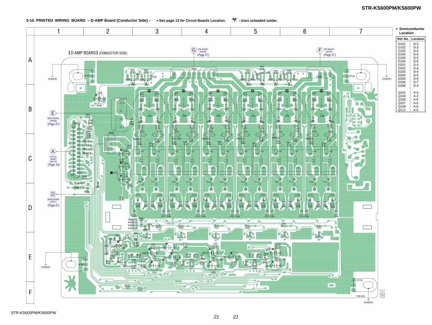
5-10. PRINTED WIRING BOARD – D-AMP Board (Conductor Side) – • See page 13 for Circuit Boards Location. : Uses unleaded solder.
CN303
CN305
CNS301
C375
C373
C211
C191
C355
L101
C216
C196
L136
L116
L126
C226
L106
C215
C195
L135
L115
L125
C225
L105
C214C221
C194
L134
C158
EP102
L114
L124
C224
L104
C213
C193
L133
L113
L123
L111
C223
L132
L103
C366
C212
C192
L122
L112
L131
C222
L102
C337
C336
C334
C333
EP103
C335
L121
C331
C329
C332
C330
C380
EP100EP101 CN306
CN307
C231 C242 C233C241 C232C246C245 C236C244 C235C243 C234
C266
R305
C403
Q105Q101
C282
D101
C283
R496
C156
C367
C292
C106
C155
R410
Q111
R226R216
C116
C256
C290
C111
R351
R211
D206
R361
R221
D106D205
C265
C105
D201 C186C185C184C154
R225R215
C115
C291
C255
C288
C264
C104
C183C153
R224
C350
R214
R402
C114
C289
C254
C286
R365
C281
C263
C103
R409
C182C152
R412
R223
R405
R364
R213
C113
R407
C287
R411
C253
C368
Q109Q107
C284
R408
R366
R403
R406R404
R362
C261
R363
C262
C102
C181C151
Q103
R222
C101
R212
C112
C285
C252C251
R483
R452
R484R453
C406
C374
C370
R401
C323
C322
C321
C320
C325
C326
R139
C324C314
C313
C312
C311
C316
C317
C315
C135
R499
C136
R487R456
C134
R464
R463
C132
R460R491
C133
R492
R461
R300
C304
C303
C302
C301
R393
C381
R302
L301
R306
C306
C308
R313
C131L100
C383
C404
L302
C384
R493
R308
R315
R396
R304
R309
R303
R462
C382
R394
C305
R498
C405
C402
FB301
R497
R450
R229
R482
D102 D202 D103 D203 D104 D204 D105
R481
R129 R231 R233
R235
R237
R451
R490
R459R458
R489
R457
R488
R495R494
L304
L305
L306
L307
L308
L309
L310
L311
L303
D208
1-864-846-
11
(11)
D-AMP BOARD (CONDUCTOR SIDE)
(CHASSIS)
(CHASSIS)(CHASSIS)
(CHASSIS)
1
25
2
24
DIGITALBOARD
CNS1101
A
SMPS BOARDCNP811
D
SMPS BOARDCNP900
E
1
4
3
1
SPK BOARDCNP500G SPK BOARD
CNP510F
1 8 1 4
A
B
C
D
E
F
1 2 3 4 5 6 7
D101 D-3D102 D-3D103 D-4D104 D-5D105 D-5D106 D-6D201 D-3D202 D-4D203 D-4D204 D-5D205 D-6D206 D-7D208 D-3
Q101 A-3Q103 A-3Q105 A-5Q107 A-5Q109 A-6Q111 A-5
• SemiconductorLocation
Ref. No. Location
(Page 15)
(Page 27)
(Page 27)
(Page 27) (Page 27)
2222
STR-KS600PM/KS600PW
STR-KS600PM/KS600PW
C335
L115
L114
L113
L105
L104
L103
TP123
R384
R383
R347
R345
R327
R326
R317
R124
R119
C319
C328
C190
C3
25
C3
26
R316
R123
C324
R382
C323
R381
C337 C336
C3
20
C3
21
C3
22
R3
29
C200
C136
C146
C186
C272 C176 R206
C271 C166 R196
C106
R237
IC106
C156
C116
L116
L106
D206
D106
C226
C216
R484
R483 R452
R453 C246
C236
C135
C145
C210 C175 R205
C209 C165 R195
R235
C155
C292
C266
R226
R216
C256
C291
D205
D105
C225
C215
R482
R481
R451
R450
C245
C235
C290
C265
R225
C3
17
C3
16
R122
R344
TP122
C333
R375
C314
R376
R377
C315
R378
C334
C3
13
C3
12
C3
11
C144
R114
C159
C185
C115
C105
C114
C104
C184
C154
C208 C174 R204
C207 C164 R194
R233
R215
C255
C289
R318
D104
D204 C224
C214
R493
R492
R462
R461
C244
C234
C150
C113
C183
C153
C103
C205 C163 R193
C206 C173 R203
R231
D203
D103
C223
C213 R464
R460 R491
R463
C243
C233
C288
C264
R224
R214
C254
C287
C286
C263
R223C143
R113
C168
C199
R213
C253
C285
C193
IC105
IC104
IC103
IC110
IC109
C327
R328
C318
R324
R325
C332
C133
C134
C198
R116
L311
L310
L309
L308
L307
L306
C178
C195
C194
C196
EP103
EP102
EP101
EP100
4716V
50nH
50nH
50nH
50nH
50nH
50nH
0
560
10k
10k
0
0
470
10k
22k
0.1
0.1
0.1
0.1
0.1
470
10k
0.1
560
0.1
0
4716V
4716V
0.1
0.1
0.1
0
0.1
0.01
0.1
0.033
0.22 0.22 3.3
0.22 0.22 3.3
1
1k
CXD9775M
0.033
1
50nH
50nH
P6SMB39AT3L13610µH
P6SMB39AT3L12610µH
1
1
10k
10k 10k
10k 100p
100p
0.01
0.1
0.22 0.22 3.3
0.22 0.22 3.3
1k
0.033
0.0022
0.0022
2.7
2.7
0.0022
0.0022
P6SMB39AT3L13510µH
P6SMB39AT3L12510µH
1
1
10k
10k
10k
10k
100p
100p
0.0022
0.0022
2.7
0.1
0.1
10k
470
4716V
0
0.1
560
560
0.1
0
4716V
0.1
0.1
0.1
0.1
22k
47p
0.033
1
1
1
1
0.033
0.033
0.22 0.22 3.3
0.22 0.22 3.3
1k
2.7
0.0022
0.0022
470
P6SMB39AT3L12410µH
P6SMB39AT3L13410µH 1
1
10k
10k
10k
10k
100p
100p
47p
1
0.033
0.033
1
0.22 0.22 3.3
0.22 0.22 3.3
1k
P6SMB39AT3L13310µH
P6SMB39AT3L12310µH
1
1 10k
10k 10k
10k
100p
100p
0.0022
0.0022
2.7
2.7
0.0022
0.0022
0.0022
0.0022
2.70.1
22k
47p
0.1
2.7
0.0022
0.0022
220035V
CXD9775M
CXD9775M
CXD9775M
CXD9788AR
CXD9788AR
0.1
0
0.1
0
0
4716V
0.01
0.01
0.1
22k
0
0
0
0
0
0
47p
220035V
220035V
220035V
A1
A2
A3
A4
A5
A6
A7
A8
A9
A10
A11
A12
A13
A14
A15
A16
A17
DATA3
BCK
LRCK
INIT
SCDT
PGMUTE
SOFT MUTE
NSP MUTE
SCLATCH3
SCSHIFT
OVFW
XFSO
RE
SE
T
SD
SCK
NSP MUTE
SOFT MUTE
PGMUTE
SCDT
SCSHIFT
SCLATCH2
INIT
LRCK
BCK
DATA2
SCK
(1/2)
STREAM PROCESSOR
STREAM PROCESSOR
DIGITAL POWER AMP
DIGITAL POWER AMP
DIGITAL POWER AMP
DIGITAL POWER AMP
(CHASSIS)
(CHASSIS)
(CHASSIS)
(CHASSIS)
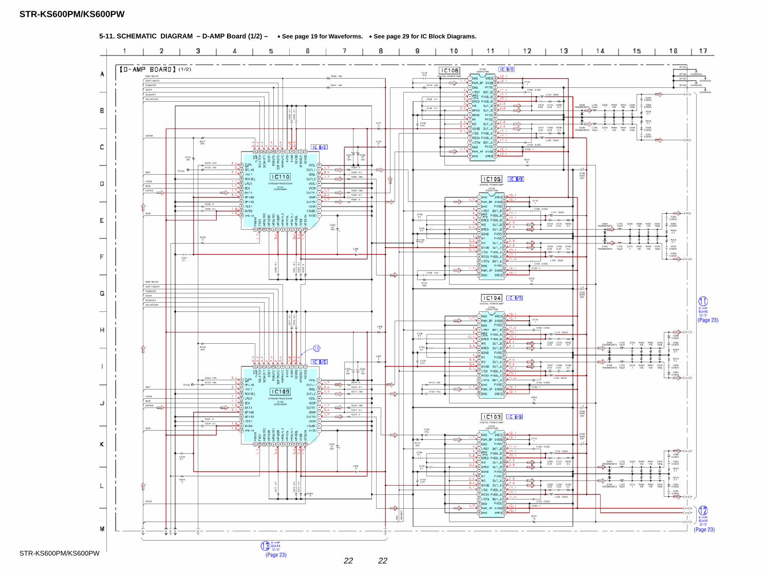
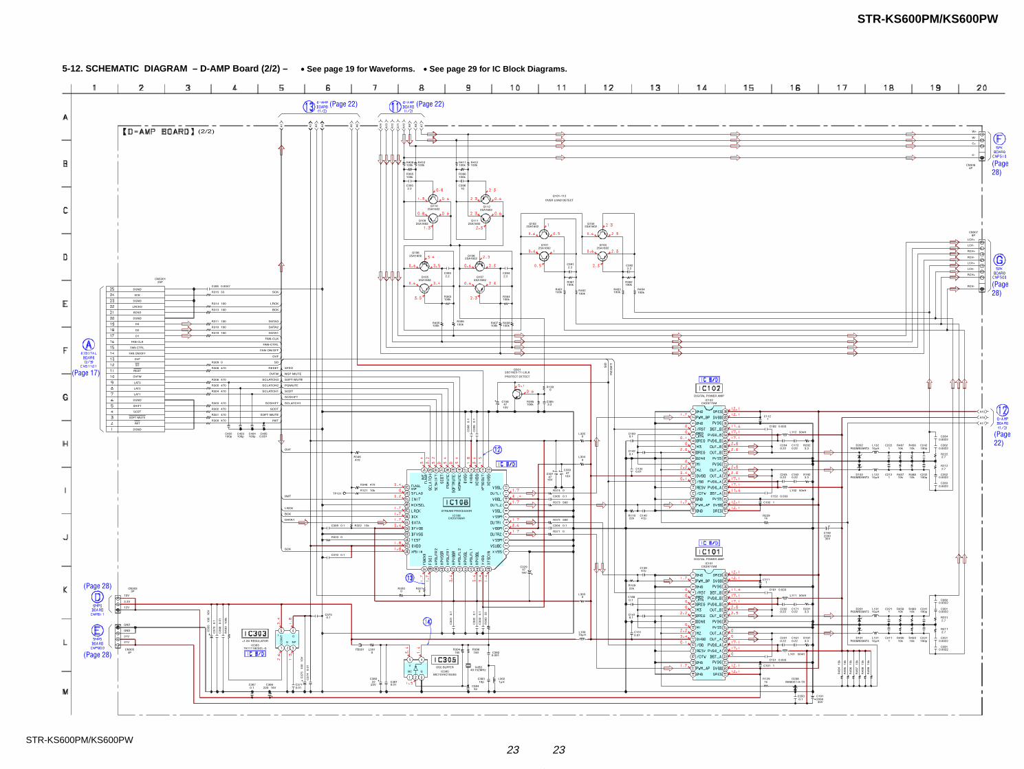
• See page 19 for Waveforms. • See page 29 for IC Block Diagrams.5-11. SCHEMATIC DIAGRAM – D-AMP Board (1/2) –
(Page 23)
(Page 23)
(Page 23)
2323
STR-KS600PM/KS600PW
STR-KS600PM/KS600PW
C329
C331
R309
Q101 Q103
Q111
Q112
Q109
Q110
C158
Q105 Q107
L112
L111
L102TP121
R406
R404R403R401
R4
00
R396
R395
R3
93
R323
R321
R319
R315
R314
R313
R311
R310
R308
R306
R305
R304
R303
C392
C3
01
C309
C310
C188
R348
R322
R121
R346
C306
C308
R374
C305
R373
R372
C304
R371
C330C
30
2
C3
03
C142
C182
R229
C139
C141
C131
R129 D208
R494
R495
R496
R497
R498
R499
C402 C403 C404 C405
R302
R351
R300
C406
CNS301
FB301
C3730.1
C380C381
C384
C382
C383
R394
C350
C374
C375
C371
C3
68
C3
70
C3
55
R320
R410 R412
R365 R366
C395 C396
C385
R409 R411
R405 R407
R139
C391
R361 R362
R402
C393
R363
C394
R364
D202
D102
C222 R487 R456 C242
C212 R457 R488 C232
C284
C262
R222
R212
C252
C283
D101
D201 C221
C211 R490
R458
R459
R489 C241
C231
C282
C261
R221
R211
C251
C281
C367 C366
CN303
CN305
CN306
IC108
IC102
IC101
CN307
R109
R110 C140
C151
C101
C132
C189
C112
C204 C172 R202
C203 C162 R192
C152
C102
C111
C181
C202 C171 R201
C201 C161 R191
L101
IC303
L301
IC305
X450
L303
L305
L304
Q301
C192
C191
R408
Q108Q106
Q102 Q104
4716V
4716V
0
2SA1602 2SA1602
2SA1602
2SA1602
2SA1602
2SA1602
4710V
2SA1602 2SA1602
50nH
50nH
50nH
100k
100k100k100k
10
0k
100
100k
22
0
0
100
33
100
100
100
100
470
470
470
470
470
2.2
0.1
0.1
0.1
0.1
470
10k
10k
470
0.1
0.1
0
0.1
560
560
0.1
0
4716V
0.1
0.1
0.1
0.033
1k
47p
0.1
0.01
1k MA8027-H-TX
15k
15k
15k
15k
15k
15k
100p 100p 100p 0.001
470
470
470
0.0047
25P
2225V 0.01
5p
0.001
10pL3021µH
1M
0.1
0.0
1
100
10V
0.01
0.0
1
0.110
01
6V
0
100k 100k
100k 100k
2.2 10
2.2
100k 100k
100k 100k
0
2.2
100k 100k
100k
2.2
100k
2.2
100k
P6SMB39AT3L13210µH
P6SMB39AT3L12210µH
1 10k 10k 100p
1 10k 10k 100p
0.0022
0.0022
2.7
2.7
0.0022
0.0022
P6SMB39AT3L12110µH
P6SMB39AT3L13110µH 1
1 10k
10k
10k
10k 100p
100p
0.0022
0.0022
2.7
2.7
0.0022
0.0022
0.1 220 16V
3P
4P
4P
CXD9788AR
CXD9775M
CXD9775M
8P
22k
22k 47p
0.033
1
0.01
0.1
1
0.22 0.22 3.3
0.22 0.22 3.3
0.033
1
1
0.033
0.22 0.22 3.3
0.22 0.22 3.3
50nH
TK11118CSCL-G
0
MC74VHC1GU04
49.152MHz
0
L10010µH
0
0
2SC1623-T1-L5L6
220035V
220035V
100k
2SA16022SA1602
2SA1602 2SA1602
A1
A2
A3
A4
A5
A6
A7
A8
A9
A10
A11
A12
A13
A14
A15
A16
A17INIT
SCDT
RESET
SD
BCK
LRCK
DATA1
BCK
LRCK
INIT
NSP MUTE
SOFT MUTE
PGMUTE
SCDT
SOFT MUTE
OVF
OVF
SCLATCH3
SCLATCH2
SCLATCH1
SCSHIFT
SCSHIFT
SCLATCH1
SCK
SCK
FAN-CLK
FAN-CTRL
FAN ON/OFF
DATA2
DATA3
OVFW
XFSO SD
RES
ET
DATA1D1
D2
D3
BCKO
LRCKO
DGND
SCDT
SHIFT
DGND
LAT1
LAT2
LAT3
INIT
12V
GND
REST
SD
DGND
SOFT MUTE
OVF
GND
C+
C-
31V
31V
12V
SCK
FAN-CLK
FAN ON/OFF
FAN-CTRL
DGND
OVFW
DGND
W-
W+
3.3V
(2/2)
NPCO
NT
+1.8V REGULATOR
NC
V
G
I O
G
OSC BUFFER
STREAM PROCESSOR
PROTECT DETECT
DIGITAL POWER AMP
DIGITAL POWER AMP
Q101-112
OVER LOAD DETECT
LCH+
LCH-
RCH+
RCH-
LCH+
LCH-
RCH+
RCH-
• See page 19 for Waveforms. • See page 29 for IC Block Diagrams.5-12. SCHEMATIC DIAGRAM – D-AMP Board (2/2) –
(Page 28)
(Page 28)
(Page 17)
(Page 22) (Page 22)
(Page28)
(Page28)
(Page22)
2424
STR-KS600PM/KS600PW
STR-KS600PM/KS600PW
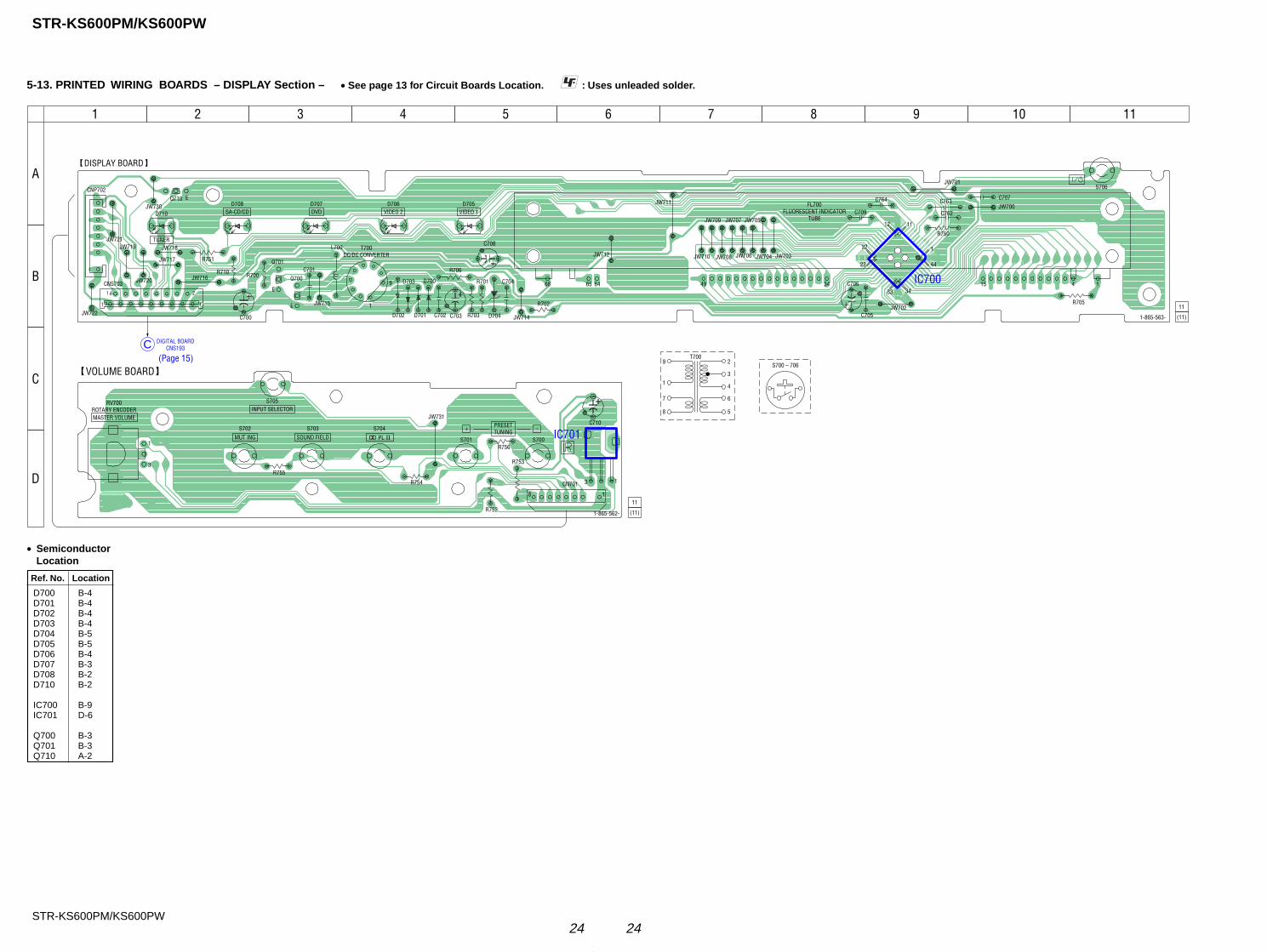
5-13. PRINTED WIRING BOARDS – DISPLAY Section – • See page 13 for Circuit Boards Location. : Uses unleaded solder.
C700
JW715
D706
L700
D703
D702
C701
D707
Q700
Q701
R700
JW700
JW701
JW702
JW703JW704
JW705
JW706
JW707
JW708
JW709
JW710
JW711
JW712
JW714
S706
C762
C707
C705
C706
C764 C763
C709
R702
R750
D705
C703
C704
C702
D700
D701 R703
R701
C708
R705
R706
D704
JW719JW721
JW722
CNS703JW716
JW717
JW718
JW720
D708
R751
Q710
D710
R710
JW730
CNP702
IC700
E
E
E
1
14153449646568
11
33
23
22
12
34
44
1-865-563-
11
(11)
DISPLAY BOARD
1
FL700FLUORESCENT INDICATOR
TUBEVIDEO 1VIDEO 2DVD
TUNER
SA-CD/CD
1
9
T700DC/DC CONVERTER
C DIGITAL BOARDCNS193
S700 – 706T700
2
3
4
6
5
9
1
7
8
S703 S704S702
S700S701
S705RV700ROTARY ENCODER
IC701R756
C710
R754
R755
R752
R753
JW731
CN701
1-865-562-
11
(11)
VOLUME BOARD
+ –PRESETTUNING
MASTER VOLUME
1
3
INPUT SELECTOR
SOUND FIELDMUT ING PL II;
1
18
3
A
B
C
D
1 2 3 4 5 6 7 8 9 10 11
D700 B-4D701 B-4D702 B-4D703 B-4D704 B-5D705 B-5D706 B-4D707 B-3D708 B-2D710 B-2
IC700 B-9IC701 D-6
Q700 B-3Q701 B-3Q710 A-2
• SemiconductorLocation
Ref. No. Location
(Page 15)
2525
STR-KS600PM/KS600PW
STR-KS600PM/KS600PW
C701
R700 C700
R701
C703
C702
C704
D704
D701
D700
D702
D703
R703R702 R710
D707
D706
D705
D708
R751R750
C763
C762
C764
C708
C709
R706
C705C706
S706CNP702
R754
R755
C710
R752
R756
IC701
CNS703
FL700
R705
C707
IC700
T700
D710
Q710
RV700
S700
S702
S704
S703
S705
S701
CN701
R753
Q700
Q701
0.022
1.8k
L70047µH
1050V
10k
1050V
0.01
0.1
HZ6.8BP-TK
1SS133T-72
1SS133T-72
1SS133T-72
1SS133T-72
470470 220
SELS5B23C
SELS523C
SELS5B23C
SELS5B23C
15082k
220p
220p
1000p
1050V
0.1
10
0.11050V
8P
1k
1k
4716V
100
1k
RPM7240-H9
17P
10
0.1
PT6315
SELS5B23C-TP15
DTC124ESA-TP
8P
10
2SD1513TP-LK
2SD1513TP-LK
VOL2A
VOL2B
SIRCS
AD(2)
AD(1)
AD(0)
+3.3V
AD(0)
AD(1)
AD(2)
VOL2A
VOL2B
SIRCS
+3.3V
49
48
47
46
45
44
43
49
48
47
46
45
44
43
45678910
11
12
34
35
36
37
38
39
40
41
42
34
35
36
37
38
39
40
41
42
4
5
6
7
8
9
10
11
12
GND
GND
+5V
+3.3V(STBY)
POWER SW
SIRCS
GND
GND
AD(0)
AD(1)
AD(2)
VOL UP
VOL DOWN
SIRCS
+3.3V(STBY)
VCC
GN
D
VOUT
FRUORESCENT INDICATOR TUBE
FRUORESCENT
INDICATOR TUBE
DRIVER,LED DRIVER
SA-CD/CD
VIDEO 2
VIDEO 1
DVD
DC/DC CONVERTER
Q700,701
OSC
TUNER
LED DRIVE
REMOTE CONTROL
RECEIVER
ROTARY ENCODER
MASTER VOLUME
PL
MUTING
PRESET
TUNING
-
SOUND
FIELD
INPUT
SELECTOR
PRESET
TUNING
+6.5V
FL_LAT
FL_CLK
FL_DIN
VOL_JOG(2A)
VOL_JOG(2B)
AD2
AD1
AD0
TUNER_LED
+
• See page 19 for Waveforms. • See page 29 for IC Block Diagrams.5-14. SCHEMATIC DIAGRAM – DISPLAY Section –
(Page 18)
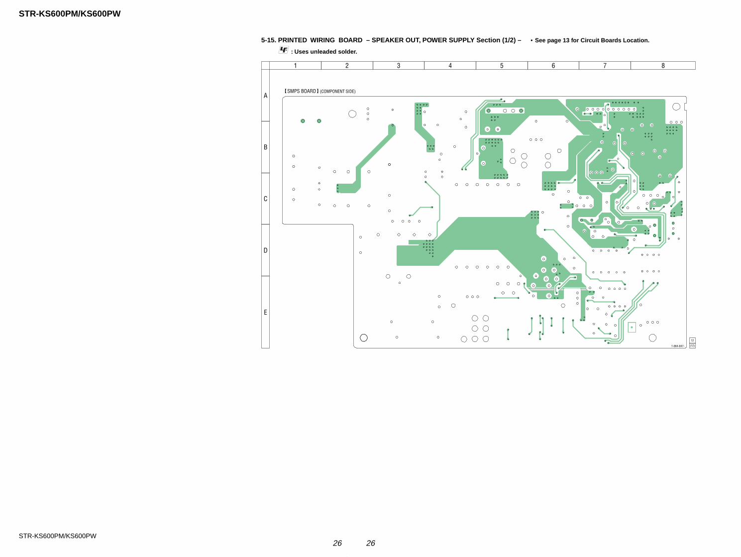
2626
STR-KS600PM/KS600PW
STR-KS600PM/KS600PW
SMPS BOARD (COMPONENT SIDE)
1-864-847-
12
(12)
A
B
C
D
E
1 2 3 4 5 6 7 8
5-15. PRINTED WIRING BOARD – SPEAKER OUT, POWER SUPPLY Section (1/2) – • See page 13 for Circuit Boards Location.
: Uses unleaded solder.
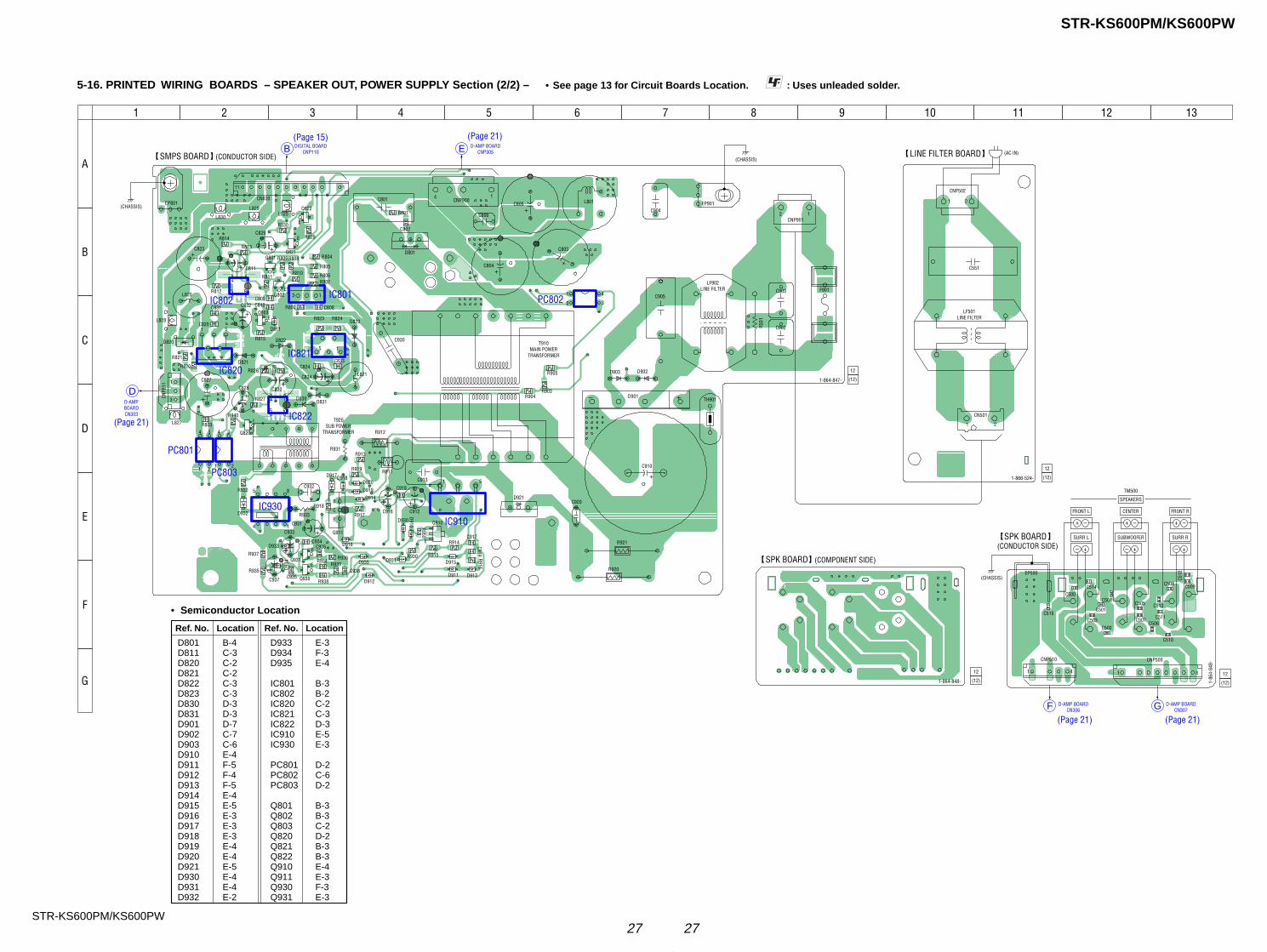
2727
STR-KS600PM/KS600PW
STR-KS600PM/KS600PW
CN820
T910
F901
CNP901
LF902LINE FILTER
C801
D901
PC802C903
C905
TH901
C803
C804
C805
C910
R920
R921
IC910
D921
L820
IC821
IC801
IC820
IC930
Q911
PC803
PC801
L821
EP801 EP901
C828
C904
C902
C930
C806
C912C916
R911
R912
C933
C937
C931
C830
C811
C829
L801
R501
C834
D801
C832
R933
D830
D822
D821
D902D903
C932
R931
D831
C827
C823
D823
C913
T920
C920
CNP900
CNP8
11
R913
Q910
C917R914
R915
C919
D915
C918
D910
D931R930
D930
D911D912
D913
R916
R918
R917
D914
D919
D918
D934
D917D920
D933
R919
R938
R939C938
C935
Q802
Q930
R934
C934C936
R936
R935
D935
R932
D932
R937
R940
R826
R827
R828
IC822R803
R802
R807
C808
R801
C802
R805
R806
R804
R820
R821
R823 R824
C809IC802
R811
Q822
R810
R813
R814
Q801
R815
C810
R812
Q803
R829
R830
Q931
D916
R950
D811
R905
R903R904
L827
L828
L830
L829L825
R809R808Q821
D820
Q820
C831
C820
C824C833
SMPS BOARD (CONDUCTOR SIDE)
1-864-847-
12
(12)
(CHASSIS)
E
E
E
E
E
E
E
E
(CHASSIS)
B DIGITAL BOARDCNP110
11 1
E D-AMP BOARDCNP305
4 1
MAIN POWERTRANSFORMER
SUB POWERTRANSFORMER
B
85
1
1
4
4
2
3
1
1
3
4
2
3
1 5
15
1 5
13
C
E
DD-AMPBOARDCN303
12
EP500
CNP500CNP510
C500
C502C503
C504C505
C506
C508 C509
C510
C511
C512
C513C515
C501
C514
C507
1 4 1 8
SPK BOARD (CONDUCTOR SIDE)
1-86
4-84
8-
12
(12)
+–
–+
SURR L
FRONT L
+–
–+
SUBWOOFER
CENTER
SPEAKERS
TM500
+–
–+
SURR R
FRONT R
(CHASSIS)
F D-AMP BOARDCN306 G D-AMP BOARD
CN307
SPK BOARD (COMPONENT SIDE)
1-864-848-
12
(12)
CNP502
C551
LF501LINE FILTER
CN501
(AC IN)LINE FILTER BOARD
1-866-524-
12
(12)
1 2
1 2
E
A
B
C
D
E
F
G
1 2 3 4 5 6 7 8 9 10 11 12 13
1 4
2 3
D933 E-3D934 F-3D935 E-4
IC801 B-3IC802 B-2IC820 C-2IC821 C-3IC822 D-3IC910 E-5IC930 E-3
PC801 D-2PC802 C-6PC803 D-2
Q801 B-3Q802 B-3Q803 C-2Q820 D-2Q821 B-3Q822 B-3Q910 E-4Q911 E-3Q930 F-3Q931 E-3
Ref. No. LocationRef. No. Location
D801 B-4D811 C-3D820 C-2D821 C-2D822 C-3D823 C-3D830 D-3D831 D-3D901 D-7D902 C-7D903 C-6D910 E-4D911 F-5D912 F-4D913 F-5D914 E-4D915 E-5D916 E-3D917 E-3D918 E-3D919 E-4D920 E-4D921 E-5D930 E-4D931 E-4D932 E-2
• Semiconductor Location
(Page 15)
(Page 21)
(Page 21)
(Page 21) (Page 21)
5-16. PRINTED WIRING BOARDS – SPEAKER OUT, POWER SUPPLY Section (2/2) – • See page 13 for Circuit Boards Location. : Uses unleaded solder.
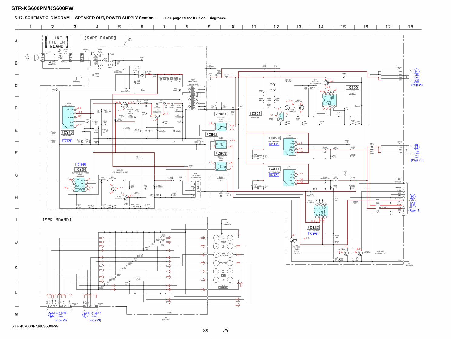
2828
STR-KS600PM/KS600PW
STR-KS600PM/KS600PW
TP905
L801 10µH
CNP900
CNP811
CN820
L829 10µH
Q822
C829
Q821
C828R829
R828
R826
R830
R827
IC822
D831
R824
R823
C827D823
D822
IC821
IC820
R820
R821
C823D821
D820
R815
R812
D811
R814C811
R813
C810R810
R811C809
C802 R801
R803
R802
R804
R805
C808
R807
IC801
Q801
R808
R809
C820C831C832
C824C833C834
Q820
C801
C805
C806C804C803
D921
TP904
TP907
TP906
C910
D903
D902
C905
LF902TP902
C903
TP901
C904
D917R918 D918
D919
D920
R919
D915D914C919
R917
D916D913
R930
D931R950
D930
R914 C917
R915
C916
D910
C912
C918
C913
R913
IC910
R904
R903
R905
C932R933
C933C934 R934
D933
IC930
R935
C935
R936 R937 C937
R938 D935
C938 R939C931
D932 R932
R931
D830
C830 R940
PC802
PC803
C930
PC801
TM500
C500
C501
C514
C515
C502
C503
C504
C505
C506
C507
C508
C509
C510
C511
C513
C512
CNP510CNP500
LF501
C551
CNP502
EP801
Q803
R806
EP500
R912R911
D911
D912
Q910Q911
R921R920 C920TH901
D901
CNP901
F901
TP903
C902
R501
CN501
T910
T920
D801
R916
Q930
Q931
D934
C936
Q802
IC802
4P
3P
11P
2SC2412K
150V
2SC2412K
22010V 100k
5.6k
470
330k
L83010µH
L82510µH
L82810µH
L82710µH
12k
SI-3025KS
11EQS04-TB5
0
0
100016V
AL01Z
11EQS04-TB5L821
220µH
SI-8120S
SI-8033JF
100
100
330010VAL01Z
EC10QS04L820
220µH
10k
1k
UDZS6.8B
1M22
50V
4.7k
0.12.2k
47k0.01
0.022 10k
2.7k
2.2k
10k
470
0.0033
220k
SE-B2
2SC2412K
2.2k
3.3k
0.10.11050V
0.10.11050V
DTC114EUA
0.047400V
220035V
0.22220035V
220035V
SARS03
390450V
10EDB60-TB5
10EDB60-TB5
0.1250V
0.0022250V
0.0022250V
EP05FA10 155355
UDZS20B
UDZS20B
33k
ISS355UDZS20B0.001
10k
UDZS15BISS355
100
ISS35510k
ISS355
1.5k 0.0047
100k
1050V
ISS355
4735V
220p
470p2kV
220
STR-F6168
220k
220k
220k
47p630V 4.7
2.250V 680p 1k
UDZS5.6B
STR-A6159
10k
47p
100k 100k 150V
1M UDZS20B
470p 100k2250V
EP05FA20 10
4.7
11EQS04-TB5
47025V
1k
TLP421
TLP421
0.0022 250V
TLP421
0.001
0.001
0.001
0.001
0.001
0.001
0.001
0.001
0.001
0.001
0.001
0.001
0.001
0.001
0.001
0.001
4P8P
0.33275V
2P
2SC2412K
6.8k
0.15W
0.332W
ISS355
ISS355
2SB11322SD2396H
68k3W
68k3W
3300p630V
RBV-606
2P
T3.15AL250V
0.0022250V
3.3M1/2W
2P
FCH20A15
3.3k
2SC2412K
2SC2412K
UDZS5.6B
0.001
2SC2412K
BA10358F
GND
GND
12V
12V
P_CONT1
STOP
GND
GND
STBY_4V
GND
GND
GND
(CHASSIS)S
W+
SW
-
C+
C-
SL
CH
+
SL
CH
-
SR
CH
+
SR
CH
-
LC
H+
LC
H-
RC
H+
RC
H-
(CHASSIS)
(CHASSIS)
(CHASSIS)
LIVE
NEUTRAL
PWM-DA
+3.3V
+12V
Q821,822
AC OFF DETECT
3.3V
31V
31V
BUFFER
G
V
+6V REGULATOR
Q801,802
BUFFER
REF
C
GND
+3.3V REGULATOR
+12V REGULATOR
+4V REGULATOR
POWER
ON/OFF
CONTROL
SPEAKERS
ISOLATOR
ISOLATOR
ISOLATOR
Q930,931
OVER CURRENT DETECTSWITCHING REGULATOR
SWITCHING
REGULATOR
B+
SWITCH
+20V
REGULATOR
(AC IN)
MAIN POWER
TRANSFORMER
SUB POWER
TRANSFORMER
1
4
3
2
2
3
1
4
2
1 4
3
SWITCHING
5-17. SCHEMATIC DIAGRAM – SPEAKER OUT, POWER SUPPLY Section – • See page 29 for IC Block Diagrams.
(Page 23) (Page 23)
(Page 18)
(Page 23)
(Page 23)
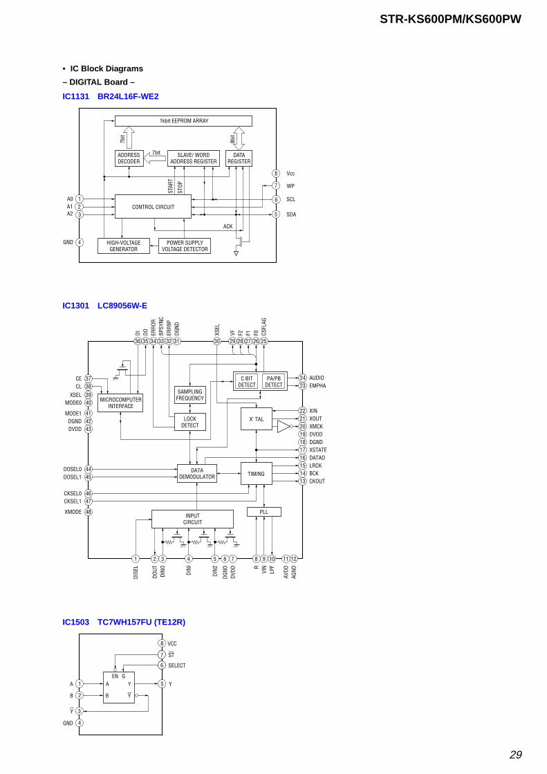
29
STR-KS600PM/KS600PW
IC1131 BR24L16F-WE2
• IC Block Diagrams
– DIGITAL Board –
123
4
5
7
8
A0A1A2
GND
Vcc
WP
SCL
SDA
1kbit EEPROM ARRAY7b
it
8bit
ADDRESSDECODER
SLAVE/ WORDADDRESS REGISTER
HIGH-VOLTAGEGENERATOR
POWER SUPPLYVOLTAGE DETECTOR
DATAREGISTER
STAR
T
STOP
ACK
CONTROL CIRCUIT6
7bit
IC1301 LC89056W-E
3837
36
2324
1 2 3 4 5
44
8 9 10
46
17
222120
3035 2526272829323334
16
45131415
47
40
41
48
CL39XSEL
CE
DI
EMPHAAUDIO
DISE
L
DOUT
DINO DINI
DIN2
6
DGND
7
DVDD
11
AVDD
12
AGND
DOSEL0
RVI
NLP
F
CKSEL0
XSTATE18 DGND19 DVDD
XINXOUTXMCK
XSEL
31
DGND
DO CSFL
AGF0F1F2VFER
R9P
BPSY
NCER
ROR
DATAO
DOSEL1CKOUTBCKLRCK
CKSEL1
MODE0
MODE142DGND43DVDD
XMODE
TIMING
MICROCOMPUTERINTERFACE
SAMPLINGFREQUENCY
C BITDETECT
PA/PBDETECT
LOCKDETECT
INPUTCIRCUIT
DATADEMODULATOR
PLL
X’ TAL
IC1503 TC7WH157FU (TE12R)
SELECT116
ST117
A 1
2
3
A
B
Y5
Y
B
GND 4
VCC8
YEN G
Y
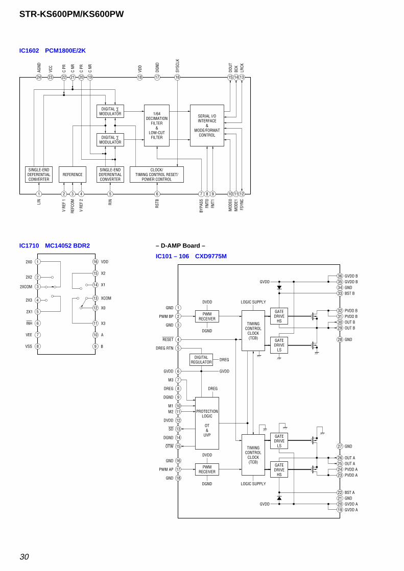
30
STR-KS600PM/KS600PW
IC1710 MC14052 BDR2
IC1602 PCM1800E/2K
SINGLE-ENDDEFERENTIALCONVERTER
REFERENCESINGLE-END
DEFERENTIALCONVERTER
DIGITAL ∑MODULATOR
DIGITAL ∑MODULATOR 1/64
DECIMATIONFILTER
&LOW-CUT
FILTER
CLOCK/TIMING CONTROL RESET/
POWER CONTROL
SERIAL I/OINTERFACE
&MODE/FORMAT
CONTROL
LIN
V RE
F 1
REFC
OM
V RE
F 2
RIN
RSTB
FMT0
BYPA
SS
FMT1
MOD
E1M
ODE0
FSYN
C
1 2 3 4 5 6 87 9 1110 12
AGND
VCC
C PR
C NR
C PR
C NR
DGND
SYSC
LK
DOUT
BCK
LRCK
VDD
24 23 22 21 20 19 17 16 15 14 1318
1
2
3
4
5
6
7
8
16
15
14
13
12
11
10
9
2X0
X2
VDD
X1
XCOM
X0
X3
A
BVSS
VEE
INH
2X1
2X3
2XCOM
2X2
IC101 – 106 CXD9775M
– D-AMP Board –
RESET 4
GND 1
GND 3
PWM BP 2
DREG RTN 5
GVDD 6
M3 7
M1 10M2 11
DVDD 12
DREG 8
DGND 9
DGND 14
GND 16
GND 18
PWMRECEIVER
TIMINGCONTROL
CLOCK(TCB)
SD 13
OTW 15
DIGITALREGULATOR
PROTECTIONLOGIC
OT&
UVP
DVDD LOGIC SUPPLY
LOGIC SUPPLY
DGND
PWM AP 17 PWMRECEIVER
DVDD
DGND
DREG
GVDD
DREG
GVDD B35GVDD B36
BST B33
PVDD B32PVDD B31OUT B30OUT B29
GND28
GND34
TIMINGCONTROL
CLOCK(TCB)
GATEDRIVE
HS
GVDD A20GVDD A19
BST A22
PVDD A23PVDD A24OUT A25OUT A26
GND27
GND21
GATEDRIVE
LS
GVDD
GVDD
GATEDRIVE
HS
GATEDRIVE
LS
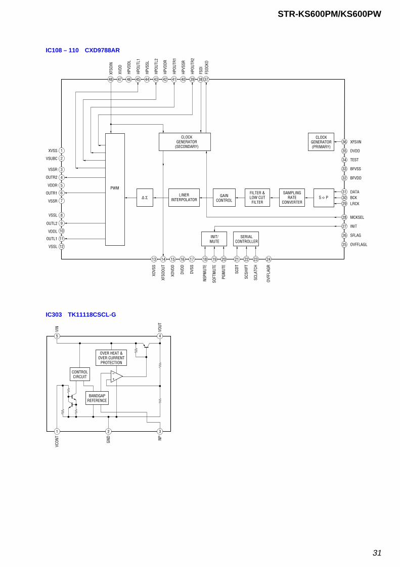
31
STR-KS600PM/KS600PW
IC108 – 110 CXD9788AR
12
11
10
9
8
7
6
5
4
3
VSUBC
XVSS
OUTR2
VSSR
OUTR1
VDDR
VSSL
VSSR
OUTL2
OUTL1
VSSL
VDDL
2
1
PWM
CLOCKGENERATOR
(SECONDARY)
CLOCKGENERATOR(PRIMARY)
31
29
25 OVFFLAGL
26 SFLAG
27 INIT
30S g PGAINCONTROL
INIT/MUTE
SAMPLINGRATE
CONVERTER
FILTER &LOW CUT
FILTER
LINERINTERPOLATOR∆ Σ
48
XFSO
IN
47
XVDD
HPVD
DL
46 45
HPOU
TL1
HPVS
SL
44 43
HPOU
TL2
HPVD
DR
42 41
HPOU
TR1
HPVS
SR
40
HPOU
TR2
39 37
FSOC
KO
38
FSOI
13
XOVS
S
14
XFSO
OUT
15
XOVD
D
16
DVDD
17
DVSS
18
NSPM
UTE
19
SOFT
MUT
E
20
PGM
UTE
SERIALCONTROLLER
21
SCDT
22
SCSH
IFT
23SC
LATC
H24
OVFF
LAGR
28 MCKSEL
32 BFVDD
33 BFVSS
34 TEST
35 DVDD
36 XFSIIN
LRCKBCKDATA
IC303 TK11118CSCL-G
1 2 3
5 4
VCON
T
GND NP
VIN
VOUT
CONTROLCIRCUIT
OVER HEAT &OVER CURRENT
PROTECTION
BANDGAPREFERENCE
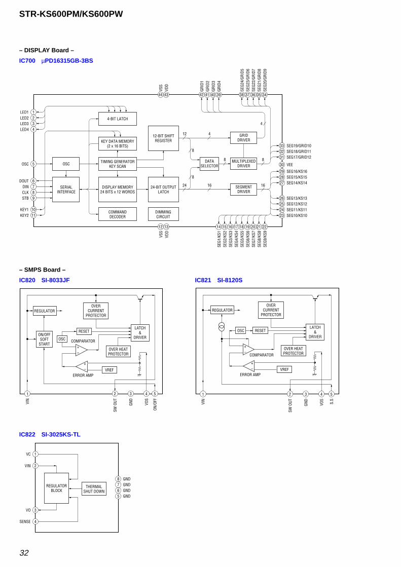
32
STR-KS600PM/KS600PW
IC700 µPD16315GB-3BS
– DISPLAY Board –
5OSC OSCDATA
SELECTOR
6DOUT7DIN8CLK9STB
10KEY111KEY2
SERIALINTERFACE
DISPLAY MEMORY24 BITS x 12 WORDS
24-BIT OUTPUTLATCH
12-BIT SHIFTREGISTER
SEGMENTDRIVER
TIMING GENERATORKEY SCAN
COMMANDDECODER
DIMMINGCIRCUIT
KEY DATA MEMORY(2 x 16 BITS)
4-BIT LATCH
1LED12LED23LED34LED4
24 16 16
12 4
8
8
4
8
27 SEG14/KS14
29 SEG16/KS16
30 VEE
28 SEG15/KS15
8 31 SEG17/GRID12
33 SEG19/GRID1032 SEG18/GRID11
23 SEG10/KS1024 SEG11/KS1125 SEG12/KS1226 SEG13/KS13
22
SEG9
/KS9
21
SEG8
/KS8
20
SEG7
/KS7
19
SEG6
/KS6
18
SEG5
/KS5
17
SEG4
/KS4
16SE
G3/K
S315
SEG2
/KS2
14
SEG1
/KS1
MULTIPLEXEDDRIVER
34
SEG2
0/GR
ID9
35
SEG2
1/GR
ID8
36
SEG2
2/GR
ID7
37
SEG2
3/GR
ID6
39
GRID
4
40
GRID
3
41
GRID
2
42
GRID
1
43
VDD
44
VSS
13
VDD
12
VSS
38
SEG2
4/GR
ID5
GRIDDRIVER
IC820 SI-8033JF
– SMPS Board –
OVERCURRENT
PROTECTOR
LATCH&
DRIVER
OVER HEATPROTECTOR
REGULATOR
ON/OFFSOFT
START+–
+–
RESET
VREF
COMPARATOR
ERROR AMP
OSC
1
VIN
2
SW O
UT
3
GND
4
VOS
5
ON/O
FF
IC821 SI-8120S
OVERCURRENT
PROTECTOR
LATCH&
DRIVER
OVER HEATPROTECTOR
REGULATOR
+–
+–
RESET
VREF
COMPARATOR
ERROR AMP
OSC
1
VIN
2
SW O
UT
3
GND
4
VOS
5
S.S
IC822 SI-3025KS-TL
VC 1
VIN 2
THERMALSHUT DOWN
REGULATORBLOCK GND6
GND5
GND8GND7
VO 3
SENSE 4
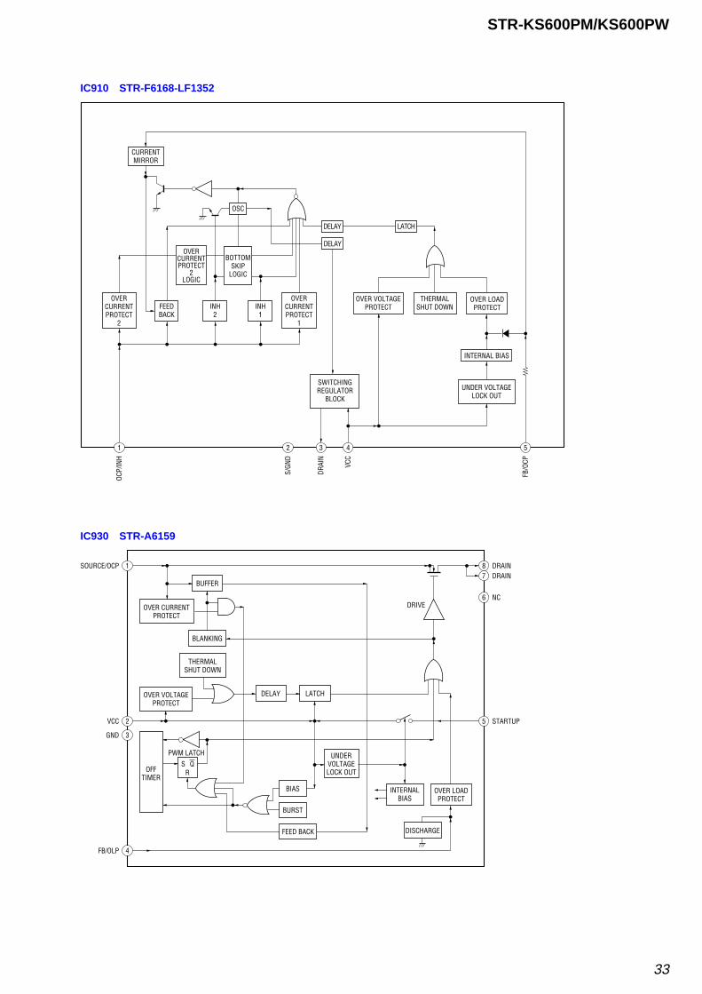
33
STR-KS600PM/KS600PW
IC910 STR-F6168-LF1352
OVERCURRENTPROTECT
2LOGIC
OSC
INTERNAL BIAS
DELAY
DELAY LATCH
CURRENTMIRROR
OVERCURRENTPROTECT
2
OVERCURRENTPROTECT
1
FEEDBACK
INH2
INH1
BOTTOMSKIP
LOGIC
OCP/
INH
1
S/GN
D
2
DRAI
N
3
VCC
4
FB/O
CP
5
UNDER VOLTAGELOCK OUT
OVER LOADPROTECT
THERMALSHUT DOWN
OVER VOLTAGEPROTECT
SWITCHINGREGULATOR
BLOCK
IC930 STR-A6159
BUFFER
OVER CURRENTPROTECT
THERMALSHUT DOWN
BLANKING
OFFTIMER
DISCHARGE
OVER VOLTAGEPROTECT
OVER LOADPROTECT
UNDERVOLTAGELOCK OUT
FEED BACK
BURST
BIAS INTERNALBIAS
DRAIN8DRAIN7
STARTUP5
NC6DRIVE
SOURCE/OCP 1
VCC 2
GND 3
FB/OLP 4
DELAY
QSR
LATCH
PWM LATCH
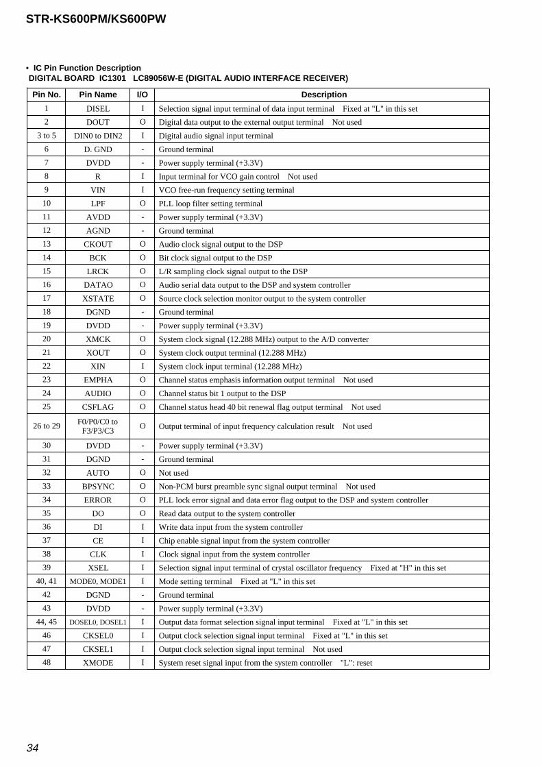
34
STR-KS600PM/KS600PW
DIGITAL BOARD IC1301 LC89056W-E (DIGITAL AUDIO INTERFACE RECEIVER)
Pin No. Pin Name I/O Description
1 DISEL I Selection signal input terminal of data input terminal Fixed at "L" in this set
2 DOUT O Digital data output to the external output terminal Not used
3 to 5 DIN0 to DIN2 I Digital audio signal input terminal
6 D. GND - Ground terminal
7 DVDD - Power supply terminal (+3.3V)
8 R I Input terminal for VCO gain control Not used
9 VIN I VCO free-run frequency setting terminal
10 LPF O PLL loop filter setting terminal
11 AVDD - Power supply terminal (+3.3V)
12 AGND - Ground terminal
13 CKOUT O Audio clock signal output to the DSP
14 BCK O Bit clock signal output to the DSP
15 LRCK O L/R sampling clock signal output to the DSP
16 DATAO O Audio serial data output to the DSP and system controller
17 XSTATE O Source clock selection monitor output to the system controller
18 DGND - Ground terminal
19 DVDD - Power supply terminal (+3.3V)
20 XMCK O System clock signal (12.288 MHz) output to the A/D converter
21 XOUT O System clock output terminal (12.288 MHz)
22 XIN I System clock input terminal (12.288 MHz)
23 EMPHA O Channel status emphasis information output terminal Not used
24 AUDIO O Channel status bit 1 output to the DSP
25 CSFLAG O Channel status head 40 bit renewal flag output terminal Not used
26 to 29 F0/P0/C0 toF3/P3/C3
O Output terminal of input frequency calculation result Not used
30 DVDD - Power supply terminal (+3.3V)
31 DGND - Ground terminal
32 AUTO O Not used
33 BPSYNC O Non-PCM burst preamble sync signal output terminal Not used
34 ERROR O PLL lock error signal and data error flag output to the DSP and system controller
35 DO O Read data output to the system controller
36 DI I Write data input from the system controller
37 CE I Chip enable signal input from the system controller
38 CLK I Clock signal input from the system controller
39 XSEL I Selection signal input terminal of crystal oscillator frequency Fixed at "H" in this set
40, 41 MODE0, MODE1 I Mode setting terminal Fixed at "L" in this set
42 DGND - Ground terminal
43 DVDD - Power supply terminal (+3.3V)
44, 45 DOSEL0, DOSEL1 I Output data format selection signal input terminal Fixed at "L" in this set
46 CKSEL0 I Output clock selection signal input terminal Fixed at "L" in this set
47 CKSEL1 I Output clock selection signal input terminal Not used
48 XMODE I System reset signal input from the system controller "L": reset
• IC Pin Function Description
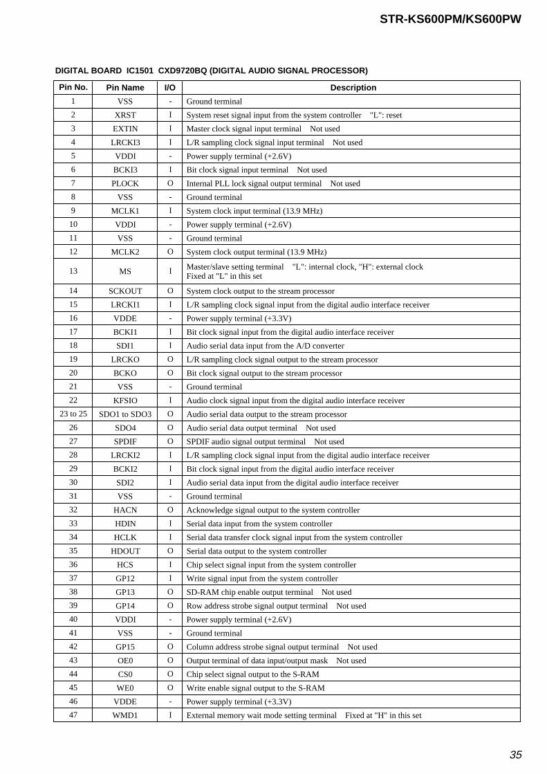
35
STR-KS600PM/KS600PW
DIGITAL BOARD IC1501 CXD9720BQ (DIGITAL AUDIO SIGNAL PROCESSOR)
Pin No. Pin Name I/O Description
1 VSS - Ground terminal
2 XRST I System reset signal input from the system controller "L": reset
3 EXTIN I Master clock signal input terminal Not used
4 LRCKI3 I L/R sampling clock signal input terminal Not used
5 VDDI - Power supply terminal (+2.6V)
6 BCKI3 I Bit clock signal input terminal Not used
7 PLOCK O Internal PLL lock signal output terminal Not used
8 VSS - Ground terminal
9 MCLK1 I System clock input terminal (13.9 MHz)
10 VDDI - Power supply terminal (+2.6V)
11 VSS - Ground terminal
12 MCLK2 O System clock output terminal (13.9 MHz)
13 MS I Master/slave setting terminal "L": internal clock, "H": external clockFixed at "L" in this set
14 SCKOUT O System clock output to the stream processor
15 LRCKI1 I L/R sampling clock signal input from the digital audio interface receiver
16 VDDE - Power supply terminal (+3.3V)
17 BCKI1 I Bit clock signal input from the digital audio interface receiver
18 SDI1 I Audio serial data input from the A/D converter
19 LRCKO O L/R sampling clock signal output to the stream processor
20 BCKO O Bit clock signal output to the stream processor
21 VSS - Ground terminal
22 KFSIO I Audio clock signal input from the digital audio interface receiver
23 to 25 SDO1 to SDO3 O Audio serial data output to the stream processor
26 SDO4 O Audio serial data output terminal Not used
27 SPDIF O SPDIF audio signal output terminal Not used
28 LRCKI2 I L/R sampling clock signal input from the digital audio interface receiver
29 BCKI2 I Bit clock signal input from the digital audio interface receiver
30 SDI2 I Audio serial data input from the digital audio interface receiver
31 VSS - Ground terminal
32 HACN O Acknowledge signal output to the system controller
33 HDIN I Serial data input from the system controller
34 HCLK I Serial data transfer clock signal input from the system controller
35 HDOUT O Serial data output to the system controller
36 HCS I Chip select signal input from the system controller
37 GP12 I Write signal input from the system controller
38 GP13 O SD-RAM chip enable output terminal Not used
39 GP14 O Row address strobe signal output terminal Not used
40 VDDI - Power supply terminal (+2.6V)
41 VSS - Ground terminal
42 GP15 O Column address strobe signal output terminal Not used
43 OE0 O Output terminal of data input/output mask Not used
44 CS0 O Chip select signal output to the S-RAM
45 WE0 O Write enable signal output to the S-RAM
46 VDDE - Power supply terminal (+3.3V)
47 WMD1 I External memory wait mode setting terminal Fixed at "H" in this set
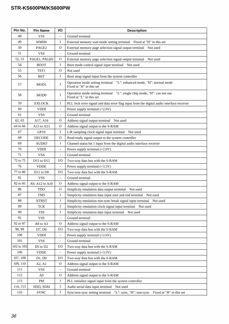
36
STR-KS600PM/KS600PW
Pin No. Pin Name I/O Description
48 VSS - Ground terminal
49 WMD0 I External memory wait mode setting terminal Fixed at "H" in this set
50 PAGE2 O External memory page selection signal output terminal Not used
51 VSS - Ground terminal
52, 53 PAGE1, PAGE0 O External memory page selection signal output terminal Not used
54 BOOT I Boot mode control signal input terminal Not used
55 TST1 O Not used
56 BST I Boot strap signal input from the system controller
57 MOD1 I Operation mode setting terminal "L": enhanced mode, "H": normal modeFixed at "H" in this set
58 MOD0 I Operation mode setting terminal "L": single chip mode, "H": can not useFixed at "L" in this set
59 EXLOCK I PLL lock error signal and data error flag input from the digital audio interface receiver
60 VDDI - Power supply terminal (+2.6V)
61 VSS - Ground terminal
62, 63 A17, A16 O Address signal output terminal Not used
64 to 66 A15 to A13 O Address signal output to the S-RAM
67 GP10 I L/R sampling clock signal input terminal Not used
68 DECODE O Read ready signal output to the system controller
69 AUDIO I Channel status bit 1 input from the digital audio interface receiver
70 VDDI - Power supply terminal (+2.6V)
71 VSS - Ground terminal
72 to 75 D15 to D12 I/O Two-way data bus with the S-RAM
76 VDDE - Power supply terminal (+3.3V)
77 to 80 D11 to D8 I/O Two-way data bus with the S-RAM
81 VSS - Ground terminal
82 to 85 A9, A12 to A10 O Address signal output to the S-RAM
86 TDO O Simplicity emulation data output terminal Not used
87 TMS I Simplicity emulation data input start and end terminal Not used
88 XTRST I Simplicity emulation non-sync break signal input terminal Not used
89 TCK I Simplicity emulation clock signal input terminal Not used
90 TDI I Simplicity emulation data input terminal Not used
91 VSS - Ground terminal
92 to 97 A8 to A3 O Address signal output to the S-RAM
98, 99 D7, D6 I/O Two-way data bus with the S-RAM
100 VDDI - Power supply terminal (+2.6V)
101 VSS - Ground terminal
102 to 105 D5 to D2 I/O Two-way data bus with the S-RAM
106 VDDE - Power supply terminal (+3.3V)
107, 108 D1, D0 I/O Two-way data bus with the S-RAM
109, 110 A2, A1 O Address signal output to the S-RAM
111 VSS - Ground terminal
112 A0 O Address signal output to the S-RAM
113 PM I PLL initialize signal input from the system controller
114, 115 SDI3, SDI4 I Audio serial data input terminal Not used
116 SYNC I Sync/non-sync setting terminal "L": sync, "H": non-sync Fixed at "H" in this set
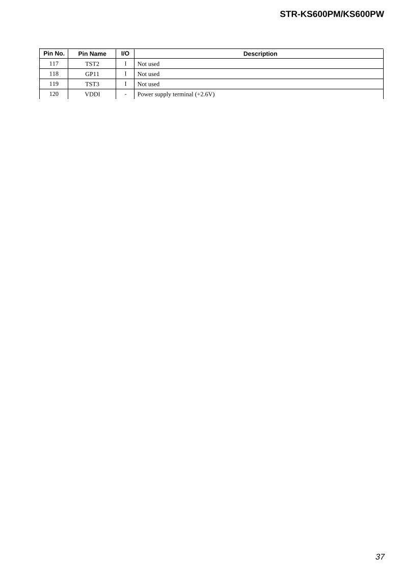
37
STR-KS600PM/KS600PW
Pin No. Pin Name I/O Description
117 TST2 I Not used
118 GP11 I Not used
119 TST3 I Not used
120 VDDI - Power supply terminal (+2.6V)
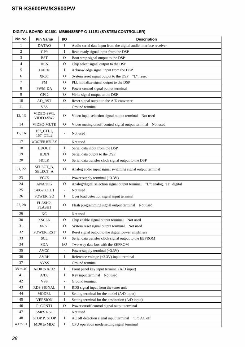
38
STR-KS600PM/KS600PW
DIGITAL BOARD IC1601 MB90488BPF-G-111E1 (SYSTEM CONTROLLER)
Pin No. Pin Name I/O Description
1 DATAO I Audio serial data input from the digital audio interface receiver
2 GP9 I Read ready signal input from the DSP
3 BST O Boot strap signal output to the DSP
4 HCS O Chip select signal output to the DSP
5 HACN I Acknowledge signal input from the DSP
6 XRST O System reset signal output to the DSP "L": reset
7 PM O PLL initialize signal output to the DSP
8 PWM-DA O Power control signal output terminal
9 GP12 O Write signal output to the DSP
10 AD_RST O Reset signal output to the A/D converter
11 VSS - Ground terminal
12, 13 VIDEO-SW1,VIDEO-SW2
O Video input selection signal output terminal Not used
14 VIDEO-MUTE O Video muting on/off control signal output terminal Not used
15, 16 157_CTL1,157_CTL2
- Not used
17 WOOFER RELAY - Not used
18 HDOUT I Serial data input from the DSP
19 HDIN O Serial data output to the DSP
20 HCLK O Serial data transfer clock signal output to the DSP
21, 22 SELECT_B,SELECT_A
O Analog audio input signal switching signal output terminal
23 VCC5 - Power supply terminal (+3.3V)
24 ANA/DIG O Analog/digital selection signal output terminal "L": analog, "H": digital
25 14052_CTL1 - Not used
26 POWER_SD I Over load detection signal input terminal
27, 28 FLASH2,FLASH1
O Flash programming signal output terminal Not used
29 NC - Not used
30 XSCEN O Chip enable signal output terminal Not used
31 XRST O System reset signal output terminal Not used
32 POWER_RST O Reset signal output to the digital power amplifiers
33 SCL O Serial data transfer clock signal output to the EEPROM
34 SDA I/O Two-way data bus with the EEPROM
35 AVCC - Power supply terminal (+3.3V)
36 AVRH I Reference voltage (+3.3V) input terminal
37 AVSS - Ground terminal
38 to 40 A/D0 to A/D2 I Front panel key input terminal (A/D input)
41 A/D3 I Key input terminal Not used
42 VSS - Ground terminal
43 RDS SIGNAL I RDS signal input from the tuner unit
44 MODEL I Setting terminal for the model (A/D input)
45 VERSION I Setting terminal for the destination (A/D input)
46 P. CONT1 O Power on/off control signal output terminal
47 SMPS RST - Not used
48 STOP P. STOP I AC off detection signal input terminal "L": AC off
49 to 51 MD0 to MD2 I CPU operation mode setting signal terminal
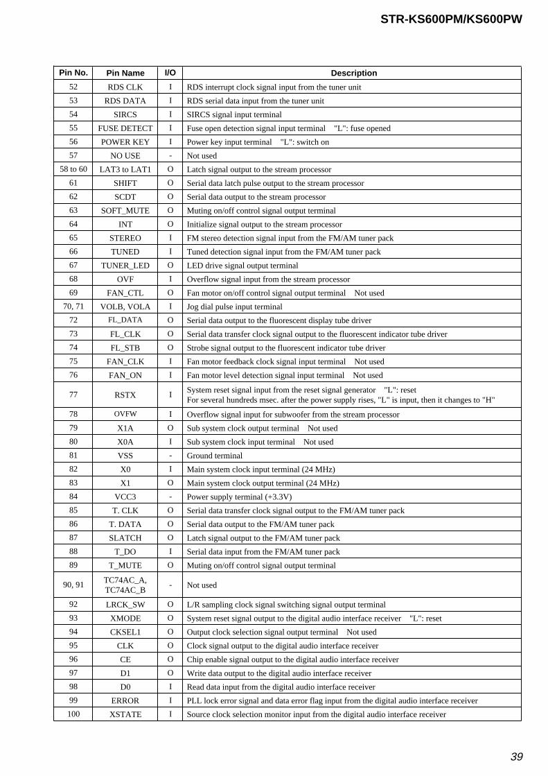
39
STR-KS600PM/KS600PW
Pin No. Pin Name I/O Description
52 RDS CLK I RDS interrupt clock signal input from the tuner unit
53 RDS DATA I RDS serial data input from the tuner unit
54 SIRCS I SIRCS signal input terminal
55 FUSE DETECT I Fuse open detection signal input terminal "L": fuse opened
56 POWER KEY I Power key input terminal "L": switch on
57 NO USE - Not used
58 to 60 LAT3 to LAT1 O Latch signal output to the stream processor
61 SHIFT O Serial data latch pulse output to the stream processor
62 SCDT O Serial data output to the stream processor
63 SOFT_MUTE O Muting on/off control signal output terminal
64 INT O Initialize signal output to the stream processor
65 STEREO I FM stereo detection signal input from the FM/AM tuner pack
66 TUNED I Tuned detection signal input from the FM/AM tuner pack
67 TUNER_LED O LED drive signal output terminal
68 OVF I Overflow signal input from the stream processor
69 FAN_CTL O Fan motor on/off control signal output terminal Not used
70, 71 VOLB, VOLA I Jog dial pulse input terminal
72 FL_DATA O Serial data output to the fluorescent display tube driver
73 FL_CLK O Serial data transfer clock signal output to the fluorescent indicator tube driver
74 FL_STB O Strobe signal output to the fluorescent indicator tube driver
75 FAN_CLK I Fan motor feedback clock signal input terminal Not used
76 FAN_ON I Fan motor level detection signal input terminal Not used
77 RSTX I System reset signal input from the reset signal generator "L": resetFor several hundreds msec. after the power supply rises, "L" is input, then it changes to "H"
78 OVFW I Overflow signal input for subwoofer from the stream processor
79 X1A O Sub system clock output terminal Not used
80 X0A I Sub system clock input terminal Not used
81 VSS - Ground terminal
82 X0 I Main system clock input terminal (24 MHz)
83 X1 O Main system clock output terminal (24 MHz)
84 VCC3 - Power supply terminal (+3.3V)
85 T. CLK O Serial data transfer clock signal output to the FM/AM tuner pack
86 T. DATA O Serial data output to the FM/AM tuner pack
87 SLATCH O Latch signal output to the FM/AM tuner pack
88 T_DO I Serial data input from the FM/AM tuner pack
89 T_MUTE O Muting on/off control signal output terminal
90, 91 TC74AC_A,TC74AC_B
- Not used
92 LRCK_SW O L/R sampling clock signal switching signal output terminal
93 XMODE O System reset signal output to the digital audio interface receiver "L": reset
94 CKSEL1 O Output clock selection signal output terminal Not used
95 CLK O Clock signal output to the digital audio interface receiver
96 CE O Chip enable signal output to the digital audio interface receiver
97 D1 O Write data output to the digital audio interface receiver
98 D0 I Read data input from the digital audio interface receiver
99 ERROR I PLL lock error signal and data error flag input from the digital audio interface receiver
100 XSTATE I Source clock selection monitor input from the digital audio interface receiver
40
STR-KS600PM/KS600PWSECTION 6
EXPLODED VIEWS
Ref. No. Part No. Description Remark Ref. No. Part No. Description Remark
1 4-254-448-01 KNOB (SL500), VOLUME2 4-977-358-01 CUSHION3 X-2050-915-2 FRONT PANEL ASSY (KS600PM)3 X-2055-641-1 FRONT PANEL ASSY (KS600PW)4 A-1097-936-A DISPLAY BOARD, COMPLETE
5 3-087-053-01 +BVTP2.6 (3CR)* 6 3-703-244-00 BUSHING (2104), CORD07 1-777-071-83 CORD, POWER
8 3-070-883-41 SCREW, TAPPING9 2-189-343-21 CASE (99BW)
* 11 1-400-052-11 FILTER, CLAMP (FERRITE CORE)RV700 1-418-725-51 ENCODER, ROTARY (12 TYPE)
(MASTER VOLUME)TN1 1-693-676-11 TUNER#2 7-685-646-79 SCREW +BVTP 3X8 TYPE2 IT-3
6-1. COVER SECTION
• Items marked “*” are not stocked since theyare seldom required for routine service. Somedelay should be anticipated when orderingthese items.
• The mechanical parts with no referencenumber in the exploded views are not supplied.
• Accessories are given in the last of theelectrical parts list.
NOTE:• -XX and -X mean standardized parts, so they
may have some difference from the originalone.
• Color Indication of Appearance PartsExample:KNOB, BALANCE (WHITE) . . . (RED)
↑ ↑Parts Color Cabinet's Color
8
8
7
6
11
9
2
5
5
4
1
2
2
#2
#2
TN1
chassis block
not supplied(VOLUME board)
notsupplied
supplied with RV700
3
RV700
#2
#2
The components identified by mark0 or dotted line with mark 0 arecritical for safety.Replace only with part numberspecified.
41
STR-KS600PM/KS600PW
6-2. CHASSIS BLOCK
Ref. No. Part No. Description Remark Ref. No. Part No. Description Remark
51 A-1097-929-A SMPS BOARD, COMPLETE52 4-857-425-00 BUSHING, 03P INSULATING53 A-1097-939-A D-AMP BOARD, COMPLETE54 1-828-650-11 WIRE (FLAT TYPE) (25 CORE)55 A-1097-941-A DIGITAL BOARD, COMPLETE
56 3-378-435-01 CUSHION, SARANET57 1-828-980-11 WIRE (FLAT TYPE) (15 CORE)
58 1-828-995-11 WIRE (FLAT TYPE) (17 CORE)59 2-598-805-01 RADIATION SHEET#1 7-685-645-79 SCREW +BVTP 3X6 TYPE2 IT-3
#2 7-685-646-79 SCREW +BVTP 3X8 TYPE2 IT-3#3 7-685-647-79 SCREW +BVTP 3X10 TYPE2 IT-3
0F901 1-532-465-33 FUSE (T3.15A/250V)
51
52
53 58
5659
57
54
55
notsupplied
not supplied(LINE FILTER board)
not supplied
not supplied(SPK board)
notsupplied
F901
#2
#1
#3
#1
#1
#1
#2
Ver. 1.1
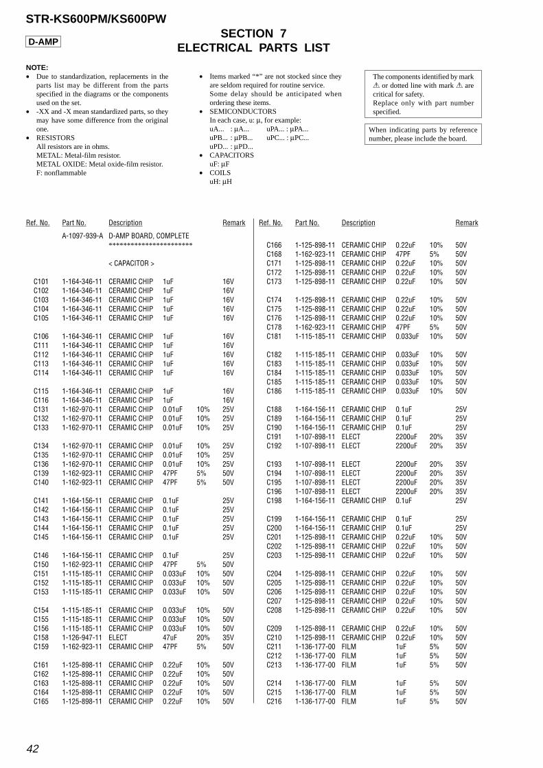
42
STR-KS600PM/KS600PWSECTION 7
ELECTRICAL PARTS LIST
Ref. No. Part No. Description Remark Ref. No. Part No. Description Remark
A-1097-939-A D-AMP BOARD, COMPLETE***********************
< CAPACITOR >
C101 1-164-346-11 CERAMIC CHIP 1uF 16VC102 1-164-346-11 CERAMIC CHIP 1uF 16VC103 1-164-346-11 CERAMIC CHIP 1uF 16VC104 1-164-346-11 CERAMIC CHIP 1uF 16VC105 1-164-346-11 CERAMIC CHIP 1uF 16V
C106 1-164-346-11 CERAMIC CHIP 1uF 16VC111 1-164-346-11 CERAMIC CHIP 1uF 16VC112 1-164-346-11 CERAMIC CHIP 1uF 16VC113 1-164-346-11 CERAMIC CHIP 1uF 16VC114 1-164-346-11 CERAMIC CHIP 1uF 16V
C115 1-164-346-11 CERAMIC CHIP 1uF 16VC116 1-164-346-11 CERAMIC CHIP 1uF 16VC131 1-162-970-11 CERAMIC CHIP 0.01uF 10% 25VC132 1-162-970-11 CERAMIC CHIP 0.01uF 10% 25VC133 1-162-970-11 CERAMIC CHIP 0.01uF 10% 25V
C134 1-162-970-11 CERAMIC CHIP 0.01uF 10% 25VC135 1-162-970-11 CERAMIC CHIP 0.01uF 10% 25VC136 1-162-970-11 CERAMIC CHIP 0.01uF 10% 25VC139 1-162-923-11 CERAMIC CHIP 47PF 5% 50VC140 1-162-923-11 CERAMIC CHIP 47PF 5% 50V
C141 1-164-156-11 CERAMIC CHIP 0.1uF 25VC142 1-164-156-11 CERAMIC CHIP 0.1uF 25VC143 1-164-156-11 CERAMIC CHIP 0.1uF 25VC144 1-164-156-11 CERAMIC CHIP 0.1uF 25VC145 1-164-156-11 CERAMIC CHIP 0.1uF 25V
C146 1-164-156-11 CERAMIC CHIP 0.1uF 25VC150 1-162-923-11 CERAMIC CHIP 47PF 5% 50VC151 1-115-185-11 CERAMIC CHIP 0.033uF 10% 50VC152 1-115-185-11 CERAMIC CHIP 0.033uF 10% 50VC153 1-115-185-11 CERAMIC CHIP 0.033uF 10% 50V
C154 1-115-185-11 CERAMIC CHIP 0.033uF 10% 50VC155 1-115-185-11 CERAMIC CHIP 0.033uF 10% 50VC156 1-115-185-11 CERAMIC CHIP 0.033uF 10% 50VC158 1-126-947-11 ELECT 47uF 20% 35VC159 1-162-923-11 CERAMIC CHIP 47PF 5% 50V
C161 1-125-898-11 CERAMIC CHIP 0.22uF 10% 50VC162 1-125-898-11 CERAMIC CHIP 0.22uF 10% 50VC163 1-125-898-11 CERAMIC CHIP 0.22uF 10% 50VC164 1-125-898-11 CERAMIC CHIP 0.22uF 10% 50VC165 1-125-898-11 CERAMIC CHIP 0.22uF 10% 50V
C166 1-125-898-11 CERAMIC CHIP 0.22uF 10% 50VC168 1-162-923-11 CERAMIC CHIP 47PF 5% 50VC171 1-125-898-11 CERAMIC CHIP 0.22uF 10% 50VC172 1-125-898-11 CERAMIC CHIP 0.22uF 10% 50VC173 1-125-898-11 CERAMIC CHIP 0.22uF 10% 50V
C174 1-125-898-11 CERAMIC CHIP 0.22uF 10% 50VC175 1-125-898-11 CERAMIC CHIP 0.22uF 10% 50VC176 1-125-898-11 CERAMIC CHIP 0.22uF 10% 50VC178 1-162-923-11 CERAMIC CHIP 47PF 5% 50VC181 1-115-185-11 CERAMIC CHIP 0.033uF 10% 50V
C182 1-115-185-11 CERAMIC CHIP 0.033uF 10% 50VC183 1-115-185-11 CERAMIC CHIP 0.033uF 10% 50VC184 1-115-185-11 CERAMIC CHIP 0.033uF 10% 50VC185 1-115-185-11 CERAMIC CHIP 0.033uF 10% 50VC186 1-115-185-11 CERAMIC CHIP 0.033uF 10% 50V
C188 1-164-156-11 CERAMIC CHIP 0.1uF 25VC189 1-164-156-11 CERAMIC CHIP 0.1uF 25VC190 1-164-156-11 CERAMIC CHIP 0.1uF 25VC191 1-107-898-11 ELECT 2200uF 20% 35VC192 1-107-898-11 ELECT 2200uF 20% 35V
C193 1-107-898-11 ELECT 2200uF 20% 35VC194 1-107-898-11 ELECT 2200uF 20% 35VC195 1-107-898-11 ELECT 2200uF 20% 35VC196 1-107-898-11 ELECT 2200uF 20% 35VC198 1-164-156-11 CERAMIC CHIP 0.1uF 25V
C199 1-164-156-11 CERAMIC CHIP 0.1uF 25VC200 1-164-156-11 CERAMIC CHIP 0.1uF 25VC201 1-125-898-11 CERAMIC CHIP 0.22uF 10% 50VC202 1-125-898-11 CERAMIC CHIP 0.22uF 10% 50VC203 1-125-898-11 CERAMIC CHIP 0.22uF 10% 50V
C204 1-125-898-11 CERAMIC CHIP 0.22uF 10% 50VC205 1-125-898-11 CERAMIC CHIP 0.22uF 10% 50VC206 1-125-898-11 CERAMIC CHIP 0.22uF 10% 50VC207 1-125-898-11 CERAMIC CHIP 0.22uF 10% 50VC208 1-125-898-11 CERAMIC CHIP 0.22uF 10% 50V
C209 1-125-898-11 CERAMIC CHIP 0.22uF 10% 50VC210 1-125-898-11 CERAMIC CHIP 0.22uF 10% 50VC211 1-136-177-00 FILM 1uF 5% 50VC212 1-136-177-00 FILM 1uF 5% 50VC213 1-136-177-00 FILM 1uF 5% 50V
C214 1-136-177-00 FILM 1uF 5% 50VC215 1-136-177-00 FILM 1uF 5% 50VC216 1-136-177-00 FILM 1uF 5% 50V
NOTE:• Due to standardization, replacements in the
parts list may be different from the partsspecified in the diagrams or the componentsused on the set.
• -XX and -X mean standardized parts, so theymay have some difference from the originalone.
• RESISTORSAll resistors are in ohms.METAL: Metal-film resistor.METAL OXIDE: Metal oxide-film resistor.F: nonflammable
• Items marked “*” are not stocked since theyare seldom required for routine service.Some delay should be anticipated whenordering these items.
• SEMICONDUCTORSIn each case, u: µ, for example:uA... : µA... uPA... : µPA...uPB... : µPB... uPC... : µPC...uPD... : µPD...
• CAPACITORSuF: µF
• COILSuH: µH
The components identified by mark0 or dotted line with mark 0 arecritical for safety.Replace only with part numberspecified.
When indicating parts by referencenumber, please include the board.
D-AMP
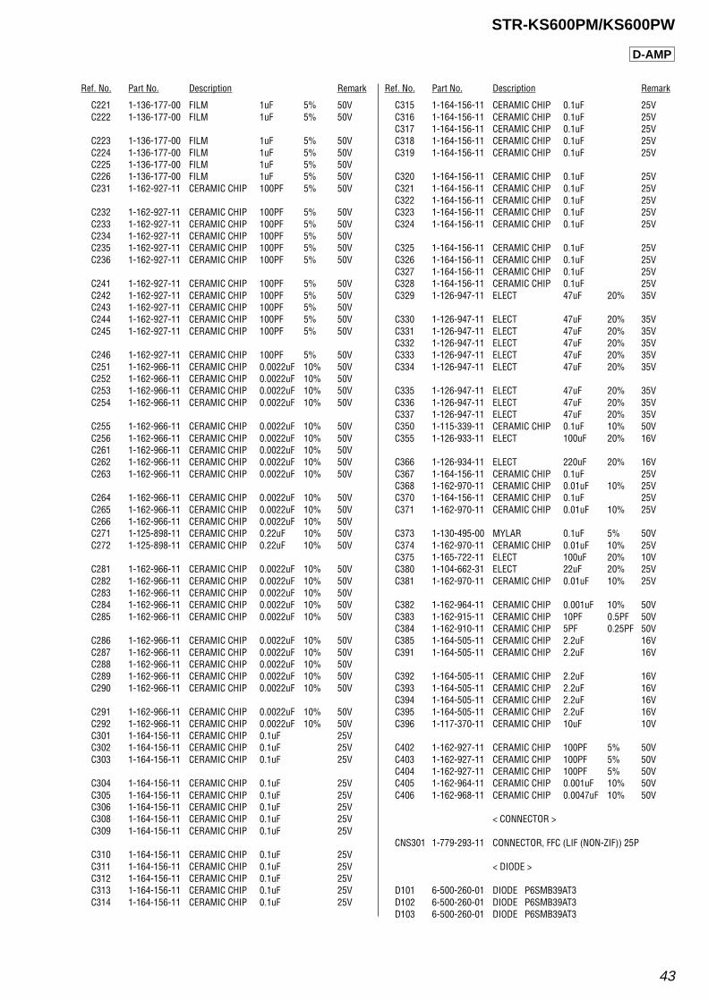
Ref. No. Part No. Description Remark Ref. No. Part No. Description Remark
43
STR-KS600PM/KS600PW
C221 1-136-177-00 FILM 1uF 5% 50VC222 1-136-177-00 FILM 1uF 5% 50V
C223 1-136-177-00 FILM 1uF 5% 50VC224 1-136-177-00 FILM 1uF 5% 50VC225 1-136-177-00 FILM 1uF 5% 50VC226 1-136-177-00 FILM 1uF 5% 50VC231 1-162-927-11 CERAMIC CHIP 100PF 5% 50V
C232 1-162-927-11 CERAMIC CHIP 100PF 5% 50VC233 1-162-927-11 CERAMIC CHIP 100PF 5% 50VC234 1-162-927-11 CERAMIC CHIP 100PF 5% 50VC235 1-162-927-11 CERAMIC CHIP 100PF 5% 50VC236 1-162-927-11 CERAMIC CHIP 100PF 5% 50V
C241 1-162-927-11 CERAMIC CHIP 100PF 5% 50VC242 1-162-927-11 CERAMIC CHIP 100PF 5% 50VC243 1-162-927-11 CERAMIC CHIP 100PF 5% 50VC244 1-162-927-11 CERAMIC CHIP 100PF 5% 50VC245 1-162-927-11 CERAMIC CHIP 100PF 5% 50V
C246 1-162-927-11 CERAMIC CHIP 100PF 5% 50VC251 1-162-966-11 CERAMIC CHIP 0.0022uF 10% 50VC252 1-162-966-11 CERAMIC CHIP 0.0022uF 10% 50VC253 1-162-966-11 CERAMIC CHIP 0.0022uF 10% 50VC254 1-162-966-11 CERAMIC CHIP 0.0022uF 10% 50V
C255 1-162-966-11 CERAMIC CHIP 0.0022uF 10% 50VC256 1-162-966-11 CERAMIC CHIP 0.0022uF 10% 50VC261 1-162-966-11 CERAMIC CHIP 0.0022uF 10% 50VC262 1-162-966-11 CERAMIC CHIP 0.0022uF 10% 50VC263 1-162-966-11 CERAMIC CHIP 0.0022uF 10% 50V
C264 1-162-966-11 CERAMIC CHIP 0.0022uF 10% 50VC265 1-162-966-11 CERAMIC CHIP 0.0022uF 10% 50VC266 1-162-966-11 CERAMIC CHIP 0.0022uF 10% 50VC271 1-125-898-11 CERAMIC CHIP 0.22uF 10% 50VC272 1-125-898-11 CERAMIC CHIP 0.22uF 10% 50V
C281 1-162-966-11 CERAMIC CHIP 0.0022uF 10% 50VC282 1-162-966-11 CERAMIC CHIP 0.0022uF 10% 50VC283 1-162-966-11 CERAMIC CHIP 0.0022uF 10% 50VC284 1-162-966-11 CERAMIC CHIP 0.0022uF 10% 50VC285 1-162-966-11 CERAMIC CHIP 0.0022uF 10% 50V
C286 1-162-966-11 CERAMIC CHIP 0.0022uF 10% 50VC287 1-162-966-11 CERAMIC CHIP 0.0022uF 10% 50VC288 1-162-966-11 CERAMIC CHIP 0.0022uF 10% 50VC289 1-162-966-11 CERAMIC CHIP 0.0022uF 10% 50VC290 1-162-966-11 CERAMIC CHIP 0.0022uF 10% 50V
C291 1-162-966-11 CERAMIC CHIP 0.0022uF 10% 50VC292 1-162-966-11 CERAMIC CHIP 0.0022uF 10% 50VC301 1-164-156-11 CERAMIC CHIP 0.1uF 25VC302 1-164-156-11 CERAMIC CHIP 0.1uF 25VC303 1-164-156-11 CERAMIC CHIP 0.1uF 25V
C304 1-164-156-11 CERAMIC CHIP 0.1uF 25VC305 1-164-156-11 CERAMIC CHIP 0.1uF 25VC306 1-164-156-11 CERAMIC CHIP 0.1uF 25VC308 1-164-156-11 CERAMIC CHIP 0.1uF 25VC309 1-164-156-11 CERAMIC CHIP 0.1uF 25V
C310 1-164-156-11 CERAMIC CHIP 0.1uF 25VC311 1-164-156-11 CERAMIC CHIP 0.1uF 25VC312 1-164-156-11 CERAMIC CHIP 0.1uF 25VC313 1-164-156-11 CERAMIC CHIP 0.1uF 25VC314 1-164-156-11 CERAMIC CHIP 0.1uF 25V
C315 1-164-156-11 CERAMIC CHIP 0.1uF 25VC316 1-164-156-11 CERAMIC CHIP 0.1uF 25VC317 1-164-156-11 CERAMIC CHIP 0.1uF 25VC318 1-164-156-11 CERAMIC CHIP 0.1uF 25VC319 1-164-156-11 CERAMIC CHIP 0.1uF 25V
C320 1-164-156-11 CERAMIC CHIP 0.1uF 25VC321 1-164-156-11 CERAMIC CHIP 0.1uF 25VC322 1-164-156-11 CERAMIC CHIP 0.1uF 25VC323 1-164-156-11 CERAMIC CHIP 0.1uF 25VC324 1-164-156-11 CERAMIC CHIP 0.1uF 25V
C325 1-164-156-11 CERAMIC CHIP 0.1uF 25VC326 1-164-156-11 CERAMIC CHIP 0.1uF 25VC327 1-164-156-11 CERAMIC CHIP 0.1uF 25VC328 1-164-156-11 CERAMIC CHIP 0.1uF 25VC329 1-126-947-11 ELECT 47uF 20% 35V
C330 1-126-947-11 ELECT 47uF 20% 35VC331 1-126-947-11 ELECT 47uF 20% 35VC332 1-126-947-11 ELECT 47uF 20% 35VC333 1-126-947-11 ELECT 47uF 20% 35VC334 1-126-947-11 ELECT 47uF 20% 35V
C335 1-126-947-11 ELECT 47uF 20% 35VC336 1-126-947-11 ELECT 47uF 20% 35VC337 1-126-947-11 ELECT 47uF 20% 35VC350 1-115-339-11 CERAMIC CHIP 0.1uF 10% 50VC355 1-126-933-11 ELECT 100uF 20% 16V
C366 1-126-934-11 ELECT 220uF 20% 16VC367 1-164-156-11 CERAMIC CHIP 0.1uF 25VC368 1-162-970-11 CERAMIC CHIP 0.01uF 10% 25VC370 1-164-156-11 CERAMIC CHIP 0.1uF 25VC371 1-162-970-11 CERAMIC CHIP 0.01uF 10% 25V
C373 1-130-495-00 MYLAR 0.1uF 5% 50VC374 1-162-970-11 CERAMIC CHIP 0.01uF 10% 25VC375 1-165-722-11 ELECT 100uF 20% 10VC380 1-104-662-31 ELECT 22uF 20% 25VC381 1-162-970-11 CERAMIC CHIP 0.01uF 10% 25V
C382 1-162-964-11 CERAMIC CHIP 0.001uF 10% 50VC383 1-162-915-11 CERAMIC CHIP 10PF 0.5PF 50VC384 1-162-910-11 CERAMIC CHIP 5PF 0.25PF 50VC385 1-164-505-11 CERAMIC CHIP 2.2uF 16VC391 1-164-505-11 CERAMIC CHIP 2.2uF 16V
C392 1-164-505-11 CERAMIC CHIP 2.2uF 16VC393 1-164-505-11 CERAMIC CHIP 2.2uF 16VC394 1-164-505-11 CERAMIC CHIP 2.2uF 16VC395 1-164-505-11 CERAMIC CHIP 2.2uF 16VC396 1-117-370-11 CERAMIC CHIP 10uF 10V
C402 1-162-927-11 CERAMIC CHIP 100PF 5% 50VC403 1-162-927-11 CERAMIC CHIP 100PF 5% 50VC404 1-162-927-11 CERAMIC CHIP 100PF 5% 50VC405 1-162-964-11 CERAMIC CHIP 0.001uF 10% 50VC406 1-162-968-11 CERAMIC CHIP 0.0047uF 10% 50V
< CONNECTOR >
CNS301 1-779-293-11 CONNECTOR, FFC (LIF (NON-ZIF)) 25P
< DIODE >
D101 6-500-260-01 DIODE P6SMB39AT3D102 6-500-260-01 DIODE P6SMB39AT3D103 6-500-260-01 DIODE P6SMB39AT3
D-AMP
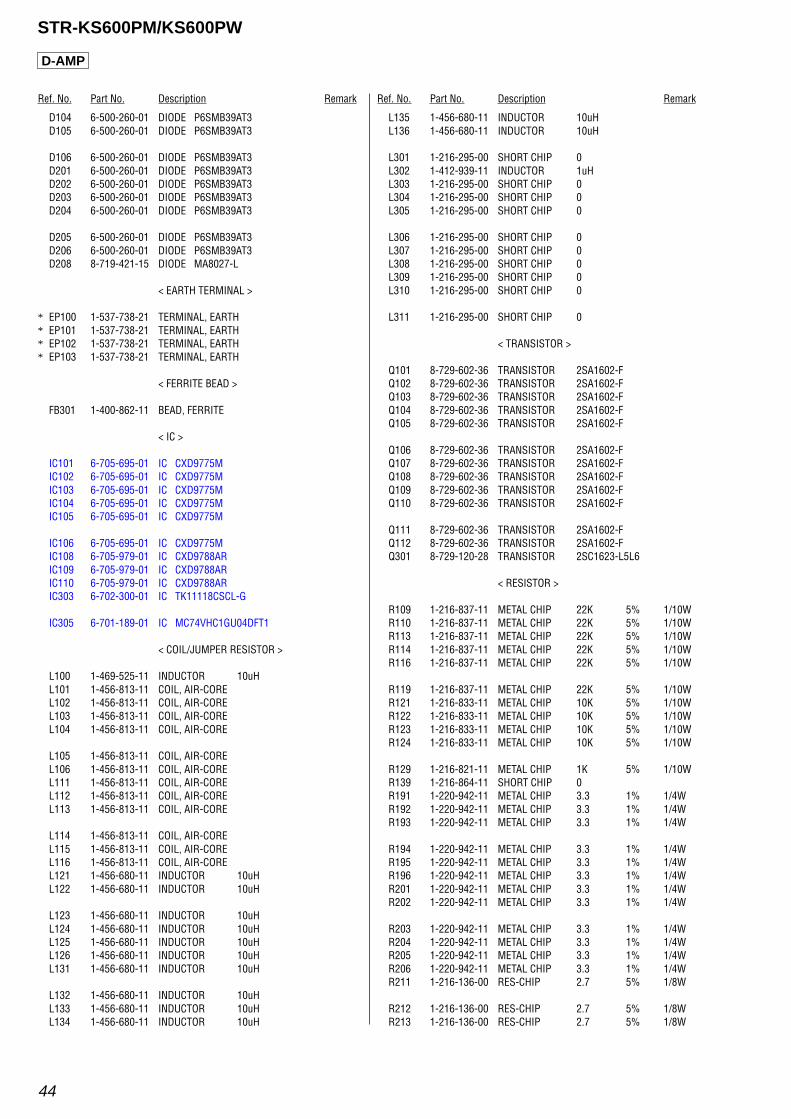
Ref. No. Part No. Description Remark Ref. No. Part No. Description Remark
44
STR-KS600PM/KS600PW
D104 6-500-260-01 DIODE P6SMB39AT3D105 6-500-260-01 DIODE P6SMB39AT3
D106 6-500-260-01 DIODE P6SMB39AT3D201 6-500-260-01 DIODE P6SMB39AT3D202 6-500-260-01 DIODE P6SMB39AT3D203 6-500-260-01 DIODE P6SMB39AT3D204 6-500-260-01 DIODE P6SMB39AT3
D205 6-500-260-01 DIODE P6SMB39AT3D206 6-500-260-01 DIODE P6SMB39AT3D208 8-719-421-15 DIODE MA8027-L
< EARTH TERMINAL >
* EP100 1-537-738-21 TERMINAL, EARTH* EP101 1-537-738-21 TERMINAL, EARTH* EP102 1-537-738-21 TERMINAL, EARTH* EP103 1-537-738-21 TERMINAL, EARTH
< FERRITE BEAD >
FB301 1-400-862-11 BEAD, FERRITE
< IC >
IC101 6-705-695-01 IC CXD9775MIC102 6-705-695-01 IC CXD9775MIC103 6-705-695-01 IC CXD9775MIC104 6-705-695-01 IC CXD9775MIC105 6-705-695-01 IC CXD9775M
IC106 6-705-695-01 IC CXD9775MIC108 6-705-979-01 IC CXD9788ARIC109 6-705-979-01 IC CXD9788ARIC110 6-705-979-01 IC CXD9788ARIC303 6-702-300-01 IC TK11118CSCL-G
IC305 6-701-189-01 IC MC74VHC1GU04DFT1
< COIL/JUMPER RESISTOR >
L100 1-469-525-11 INDUCTOR 10uHL101 1-456-813-11 COIL, AIR-COREL102 1-456-813-11 COIL, AIR-COREL103 1-456-813-11 COIL, AIR-COREL104 1-456-813-11 COIL, AIR-CORE
L105 1-456-813-11 COIL, AIR-COREL106 1-456-813-11 COIL, AIR-COREL111 1-456-813-11 COIL, AIR-COREL112 1-456-813-11 COIL, AIR-COREL113 1-456-813-11 COIL, AIR-CORE
L114 1-456-813-11 COIL, AIR-COREL115 1-456-813-11 COIL, AIR-COREL116 1-456-813-11 COIL, AIR-COREL121 1-456-680-11 INDUCTOR 10uHL122 1-456-680-11 INDUCTOR 10uH
L123 1-456-680-11 INDUCTOR 10uHL124 1-456-680-11 INDUCTOR 10uHL125 1-456-680-11 INDUCTOR 10uHL126 1-456-680-11 INDUCTOR 10uHL131 1-456-680-11 INDUCTOR 10uH
L132 1-456-680-11 INDUCTOR 10uHL133 1-456-680-11 INDUCTOR 10uHL134 1-456-680-11 INDUCTOR 10uH
L135 1-456-680-11 INDUCTOR 10uHL136 1-456-680-11 INDUCTOR 10uH
L301 1-216-295-00 SHORT CHIP 0L302 1-412-939-11 INDUCTOR 1uHL303 1-216-295-00 SHORT CHIP 0L304 1-216-295-00 SHORT CHIP 0L305 1-216-295-00 SHORT CHIP 0
L306 1-216-295-00 SHORT CHIP 0L307 1-216-295-00 SHORT CHIP 0L308 1-216-295-00 SHORT CHIP 0L309 1-216-295-00 SHORT CHIP 0L310 1-216-295-00 SHORT CHIP 0
L311 1-216-295-00 SHORT CHIP 0
< TRANSISTOR >
Q101 8-729-602-36 TRANSISTOR 2SA1602-FQ102 8-729-602-36 TRANSISTOR 2SA1602-FQ103 8-729-602-36 TRANSISTOR 2SA1602-FQ104 8-729-602-36 TRANSISTOR 2SA1602-FQ105 8-729-602-36 TRANSISTOR 2SA1602-F
Q106 8-729-602-36 TRANSISTOR 2SA1602-FQ107 8-729-602-36 TRANSISTOR 2SA1602-FQ108 8-729-602-36 TRANSISTOR 2SA1602-FQ109 8-729-602-36 TRANSISTOR 2SA1602-FQ110 8-729-602-36 TRANSISTOR 2SA1602-F
Q111 8-729-602-36 TRANSISTOR 2SA1602-FQ112 8-729-602-36 TRANSISTOR 2SA1602-FQ301 8-729-120-28 TRANSISTOR 2SC1623-L5L6
< RESISTOR >
R109 1-216-837-11 METAL CHIP 22K 5% 1/10WR110 1-216-837-11 METAL CHIP 22K 5% 1/10WR113 1-216-837-11 METAL CHIP 22K 5% 1/10WR114 1-216-837-11 METAL CHIP 22K 5% 1/10WR116 1-216-837-11 METAL CHIP 22K 5% 1/10W
R119 1-216-837-11 METAL CHIP 22K 5% 1/10WR121 1-216-833-11 METAL CHIP 10K 5% 1/10WR122 1-216-833-11 METAL CHIP 10K 5% 1/10WR123 1-216-833-11 METAL CHIP 10K 5% 1/10WR124 1-216-833-11 METAL CHIP 10K 5% 1/10W
R129 1-216-821-11 METAL CHIP 1K 5% 1/10WR139 1-216-864-11 SHORT CHIP 0R191 1-220-942-11 METAL CHIP 3.3 1% 1/4WR192 1-220-942-11 METAL CHIP 3.3 1% 1/4WR193 1-220-942-11 METAL CHIP 3.3 1% 1/4W
R194 1-220-942-11 METAL CHIP 3.3 1% 1/4WR195 1-220-942-11 METAL CHIP 3.3 1% 1/4WR196 1-220-942-11 METAL CHIP 3.3 1% 1/4WR201 1-220-942-11 METAL CHIP 3.3 1% 1/4WR202 1-220-942-11 METAL CHIP 3.3 1% 1/4W
R203 1-220-942-11 METAL CHIP 3.3 1% 1/4WR204 1-220-942-11 METAL CHIP 3.3 1% 1/4WR205 1-220-942-11 METAL CHIP 3.3 1% 1/4WR206 1-220-942-11 METAL CHIP 3.3 1% 1/4WR211 1-216-136-00 RES-CHIP 2.7 5% 1/8W
R212 1-216-136-00 RES-CHIP 2.7 5% 1/8WR213 1-216-136-00 RES-CHIP 2.7 5% 1/8W
D-AMP
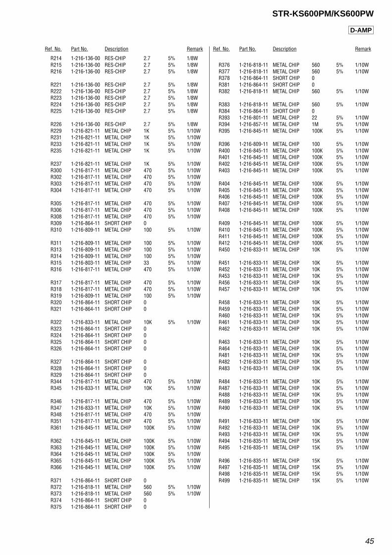
Ref. No. Part No. Description Remark Ref. No. Part No. Description Remark
45
STR-KS600PM/KS600PW
R214 1-216-136-00 RES-CHIP 2.7 5% 1/8WR215 1-216-136-00 RES-CHIP 2.7 5% 1/8WR216 1-216-136-00 RES-CHIP 2.7 5% 1/8W
R221 1-216-136-00 RES-CHIP 2.7 5% 1/8WR222 1-216-136-00 RES-CHIP 2.7 5% 1/8WR223 1-216-136-00 RES-CHIP 2.7 5% 1/8WR224 1-216-136-00 RES-CHIP 2.7 5% 1/8WR225 1-216-136-00 RES-CHIP 2.7 5% 1/8W
R226 1-216-136-00 RES-CHIP 2.7 5% 1/8WR229 1-216-821-11 METAL CHIP 1K 5% 1/10WR231 1-216-821-11 METAL CHIP 1K 5% 1/10WR233 1-216-821-11 METAL CHIP 1K 5% 1/10WR235 1-216-821-11 METAL CHIP 1K 5% 1/10W
R237 1-216-821-11 METAL CHIP 1K 5% 1/10WR300 1-216-817-11 METAL CHIP 470 5% 1/10WR302 1-216-817-11 METAL CHIP 470 5% 1/10WR303 1-216-817-11 METAL CHIP 470 5% 1/10WR304 1-216-817-11 METAL CHIP 470 5% 1/10W
R305 1-216-817-11 METAL CHIP 470 5% 1/10WR306 1-216-817-11 METAL CHIP 470 5% 1/10WR308 1-216-817-11 METAL CHIP 470 5% 1/10WR309 1-216-864-11 SHORT CHIP 0R310 1-216-809-11 METAL CHIP 100 5% 1/10W
R311 1-216-809-11 METAL CHIP 100 5% 1/10WR313 1-216-809-11 METAL CHIP 100 5% 1/10WR314 1-216-809-11 METAL CHIP 100 5% 1/10WR315 1-216-803-11 METAL CHIP 33 5% 1/10WR316 1-216-817-11 METAL CHIP 470 5% 1/10W
R317 1-216-817-11 METAL CHIP 470 5% 1/10WR318 1-216-817-11 METAL CHIP 470 5% 1/10WR319 1-216-809-11 METAL CHIP 100 5% 1/10WR320 1-216-864-11 SHORT CHIP 0R321 1-216-864-11 SHORT CHIP 0
R322 1-216-833-11 METAL CHIP 10K 5% 1/10WR323 1-216-864-11 SHORT CHIP 0R324 1-216-864-11 SHORT CHIP 0R325 1-216-864-11 SHORT CHIP 0R326 1-216-864-11 SHORT CHIP 0
R327 1-216-864-11 SHORT CHIP 0R328 1-216-864-11 SHORT CHIP 0R329 1-216-864-11 SHORT CHIP 0R344 1-216-817-11 METAL CHIP 470 5% 1/10WR345 1-216-833-11 METAL CHIP 10K 5% 1/10W
R346 1-216-817-11 METAL CHIP 470 5% 1/10WR347 1-216-833-11 METAL CHIP 10K 5% 1/10WR348 1-216-817-11 METAL CHIP 470 5% 1/10WR351 1-216-817-11 METAL CHIP 470 5% 1/10WR361 1-216-845-11 METAL CHIP 100K 5% 1/10W
R362 1-216-845-11 METAL CHIP 100K 5% 1/10WR363 1-216-845-11 METAL CHIP 100K 5% 1/10WR364 1-216-845-11 METAL CHIP 100K 5% 1/10WR365 1-216-845-11 METAL CHIP 100K 5% 1/10WR366 1-216-845-11 METAL CHIP 100K 5% 1/10W
R371 1-216-864-11 SHORT CHIP 0R372 1-216-818-11 METAL CHIP 560 5% 1/10WR373 1-216-818-11 METAL CHIP 560 5% 1/10WR374 1-216-864-11 SHORT CHIP 0R375 1-216-864-11 SHORT CHIP 0
R376 1-216-818-11 METAL CHIP 560 5% 1/10WR377 1-216-818-11 METAL CHIP 560 5% 1/10WR378 1-216-864-11 SHORT CHIP 0R381 1-216-864-11 SHORT CHIP 0R382 1-216-818-11 METAL CHIP 560 5% 1/10W
R383 1-216-818-11 METAL CHIP 560 5% 1/10WR384 1-216-864-11 SHORT CHIP 0R393 1-216-801-11 METAL CHIP 22 5% 1/10WR394 1-216-857-11 METAL CHIP 1M 5% 1/10WR395 1-216-845-11 METAL CHIP 100K 5% 1/10W
R396 1-216-809-11 METAL CHIP 100 5% 1/10WR400 1-216-845-11 METAL CHIP 100K 5% 1/10WR401 1-216-845-11 METAL CHIP 100K 5% 1/10WR402 1-216-845-11 METAL CHIP 100K 5% 1/10WR403 1-216-845-11 METAL CHIP 100K 5% 1/10W
R404 1-216-845-11 METAL CHIP 100K 5% 1/10WR405 1-216-845-11 METAL CHIP 100K 5% 1/10WR406 1-216-845-11 METAL CHIP 100K 5% 1/10WR407 1-216-845-11 METAL CHIP 100K 5% 1/10WR408 1-216-845-11 METAL CHIP 100K 5% 1/10W
R409 1-216-845-11 METAL CHIP 100K 5% 1/10WR410 1-216-845-11 METAL CHIP 100K 5% 1/10WR411 1-216-845-11 METAL CHIP 100K 5% 1/10WR412 1-216-845-11 METAL CHIP 100K 5% 1/10WR450 1-216-833-11 METAL CHIP 10K 5% 1/10W
R451 1-216-833-11 METAL CHIP 10K 5% 1/10WR452 1-216-833-11 METAL CHIP 10K 5% 1/10WR453 1-216-833-11 METAL CHIP 10K 5% 1/10WR456 1-216-833-11 METAL CHIP 10K 5% 1/10WR457 1-216-833-11 METAL CHIP 10K 5% 1/10W
R458 1-216-833-11 METAL CHIP 10K 5% 1/10WR459 1-216-833-11 METAL CHIP 10K 5% 1/10WR460 1-216-833-11 METAL CHIP 10K 5% 1/10WR461 1-216-833-11 METAL CHIP 10K 5% 1/10WR462 1-216-833-11 METAL CHIP 10K 5% 1/10W
R463 1-216-833-11 METAL CHIP 10K 5% 1/10WR464 1-216-833-11 METAL CHIP 10K 5% 1/10WR481 1-216-833-11 METAL CHIP 10K 5% 1/10WR482 1-216-833-11 METAL CHIP 10K 5% 1/10WR483 1-216-833-11 METAL CHIP 10K 5% 1/10W
R484 1-216-833-11 METAL CHIP 10K 5% 1/10WR487 1-216-833-11 METAL CHIP 10K 5% 1/10WR488 1-216-833-11 METAL CHIP 10K 5% 1/10WR489 1-216-833-11 METAL CHIP 10K 5% 1/10WR490 1-216-833-11 METAL CHIP 10K 5% 1/10W
R491 1-216-833-11 METAL CHIP 10K 5% 1/10WR492 1-216-833-11 METAL CHIP 10K 5% 1/10WR493 1-216-833-11 METAL CHIP 10K 5% 1/10WR494 1-216-835-11 METAL CHIP 15K 5% 1/10WR495 1-216-835-11 METAL CHIP 15K 5% 1/10W
R496 1-216-835-11 METAL CHIP 15K 5% 1/10WR497 1-216-835-11 METAL CHIP 15K 5% 1/10WR498 1-216-835-11 METAL CHIP 15K 5% 1/10WR499 1-216-835-11 METAL CHIP 15K 5% 1/10W
D-AMP
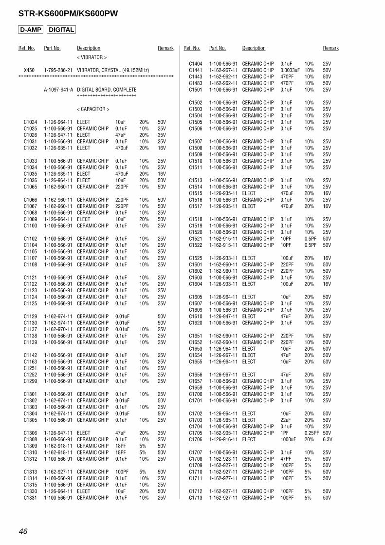
Ref. No. Part No. Description Remark Ref. No. Part No. Description Remark
46
STR-KS600PM/KS600PW
DIGITAL
< VIBRATOR >
X450 1-795-286-21 VIBRATOR, CRYSTAL (49.152MHz)************************************************************
A-1097-941-A DIGITAL BOARD, COMPLETE***********************
< CAPACITOR >
C1024 1-126-964-11 ELECT 10uF 20% 50VC1025 1-100-566-91 CERAMIC CHIP 0.1uF 10% 25VC1026 1-126-947-11 ELECT 47uF 20% 35VC1031 1-100-566-91 CERAMIC CHIP 0.1uF 10% 25VC1032 1-126-935-11 ELECT 470uF 20% 16V
C1033 1-100-566-91 CERAMIC CHIP 0.1uF 10% 25VC1034 1-100-566-91 CERAMIC CHIP 0.1uF 10% 25VC1035 1-126-935-11 ELECT 470uF 20% 16VC1036 1-126-964-11 ELECT 10uF 20% 50VC1065 1-162-960-11 CERAMIC CHIP 220PF 10% 50V
C1066 1-162-960-11 CERAMIC CHIP 220PF 10% 50VC1067 1-162-960-11 CERAMIC CHIP 220PF 10% 50VC1068 1-100-566-91 CERAMIC CHIP 0.1uF 10% 25VC1069 1-126-964-11 ELECT 10uF 20% 50VC1100 1-100-566-91 CERAMIC CHIP 0.1uF 10% 25V
C1102 1-100-566-91 CERAMIC CHIP 0.1uF 10% 25VC1104 1-100-566-91 CERAMIC CHIP 0.1uF 10% 25VC1105 1-100-566-91 CERAMIC CHIP 0.1uF 10% 25VC1107 1-100-566-91 CERAMIC CHIP 0.1uF 10% 25VC1108 1-100-566-91 CERAMIC CHIP 0.1uF 10% 25V
C1121 1-100-566-91 CERAMIC CHIP 0.1uF 10% 25VC1122 1-100-566-91 CERAMIC CHIP 0.1uF 10% 25VC1123 1-100-566-91 CERAMIC CHIP 0.1uF 10% 25VC1124 1-100-566-91 CERAMIC CHIP 0.1uF 10% 25VC1125 1-100-566-91 CERAMIC CHIP 0.1uF 10% 25V
C1129 1-162-974-11 CERAMIC CHIP 0.01uF 50VC1130 1-162-974-11 CERAMIC CHIP 0.01uF 50VC1137 1-162-970-11 CERAMIC CHIP 0.01uF 10% 25VC1138 1-100-566-91 CERAMIC CHIP 0.1uF 10% 25VC1139 1-100-566-91 CERAMIC CHIP 0.1uF 10% 25V
C1142 1-100-566-91 CERAMIC CHIP 0.1uF 10% 25VC1163 1-100-566-91 CERAMIC CHIP 0.1uF 10% 25VC1251 1-100-566-91 CERAMIC CHIP 0.1uF 10% 25VC1252 1-100-566-91 CERAMIC CHIP 0.1uF 10% 25VC1299 1-100-566-91 CERAMIC CHIP 0.1uF 10% 25V
C1301 1-100-566-91 CERAMIC CHIP 0.1uF 10% 25VC1302 1-162-974-11 CERAMIC CHIP 0.01uF 50VC1303 1-100-566-91 CERAMIC CHIP 0.1uF 10% 25VC1304 1-162-974-11 CERAMIC CHIP 0.01uF 50VC1305 1-100-566-91 CERAMIC CHIP 0.1uF 10% 25V
C1306 1-126-947-11 ELECT 47uF 20% 35VC1308 1-100-566-91 CERAMIC CHIP 0.1uF 10% 25VC1309 1-162-918-11 CERAMIC CHIP 18PF 5% 50VC1310 1-162-918-11 CERAMIC CHIP 18PF 5% 50VC1312 1-100-566-91 CERAMIC CHIP 0.1uF 10% 25V
C1313 1-162-927-11 CERAMIC CHIP 100PF 5% 50VC1314 1-100-566-91 CERAMIC CHIP 0.1uF 10% 25VC1315 1-100-566-91 CERAMIC CHIP 0.1uF 10% 25VC1330 1-126-964-11 ELECT 10uF 20% 50VC1331 1-100-566-91 CERAMIC CHIP 0.1uF 10% 25V
C1404 1-100-566-91 CERAMIC CHIP 0.1uF 10% 25VC1441 1-162-967-11 CERAMIC CHIP 0.0033uF 10% 50VC1443 1-162-962-11 CERAMIC CHIP 470PF 10% 50VC1483 1-162-962-11 CERAMIC CHIP 470PF 10% 50VC1501 1-100-566-91 CERAMIC CHIP 0.1uF 10% 25V
C1502 1-100-566-91 CERAMIC CHIP 0.1uF 10% 25VC1503 1-100-566-91 CERAMIC CHIP 0.1uF 10% 25VC1504 1-100-566-91 CERAMIC CHIP 0.1uF 10% 25VC1505 1-100-566-91 CERAMIC CHIP 0.1uF 10% 25VC1506 1-100-566-91 CERAMIC CHIP 0.1uF 10% 25V
C1507 1-100-566-91 CERAMIC CHIP 0.1uF 10% 25VC1508 1-100-566-91 CERAMIC CHIP 0.1uF 10% 25VC1509 1-100-566-91 CERAMIC CHIP 0.1uF 10% 25VC1510 1-100-566-91 CERAMIC CHIP 0.1uF 10% 25VC1511 1-100-566-91 CERAMIC CHIP 0.1uF 10% 25V
C1513 1-100-566-91 CERAMIC CHIP 0.1uF 10% 25VC1514 1-100-566-91 CERAMIC CHIP 0.1uF 10% 25VC1515 1-126-935-11 ELECT 470uF 20% 16VC1516 1-100-566-91 CERAMIC CHIP 0.1uF 10% 25VC1517 1-126-935-11 ELECT 470uF 20% 16V
C1518 1-100-566-91 CERAMIC CHIP 0.1uF 10% 25VC1519 1-100-566-91 CERAMIC CHIP 0.1uF 10% 25VC1520 1-100-566-91 CERAMIC CHIP 0.1uF 10% 25VC1521 1-162-915-11 CERAMIC CHIP 10PF 0.5PF 50VC1522 1-162-915-11 CERAMIC CHIP 10PF 0.5PF 50V
C1525 1-126-933-11 ELECT 100uF 20% 16VC1601 1-162-960-11 CERAMIC CHIP 220PF 10% 50VC1602 1-162-960-11 CERAMIC CHIP 220PF 10% 50VC1603 1-100-566-91 CERAMIC CHIP 0.1uF 10% 25VC1604 1-126-933-11 ELECT 100uF 20% 16V
C1605 1-126-964-11 ELECT 10uF 20% 50VC1607 1-100-566-91 CERAMIC CHIP 0.1uF 10% 25VC1609 1-100-566-91 CERAMIC CHIP 0.1uF 10% 25VC1610 1-126-947-11 ELECT 47uF 20% 35VC1620 1-100-566-91 CERAMIC CHIP 0.1uF 10% 25V
C1651 1-162-960-11 CERAMIC CHIP 220PF 10% 50VC1652 1-162-960-11 CERAMIC CHIP 220PF 10% 50VC1653 1-126-964-11 ELECT 10uF 20% 50VC1654 1-126-967-11 ELECT 47uF 20% 50VC1655 1-126-964-11 ELECT 10uF 20% 50V
C1656 1-126-967-11 ELECT 47uF 20% 50VC1657 1-100-566-91 CERAMIC CHIP 0.1uF 10% 25VC1659 1-100-566-91 CERAMIC CHIP 0.1uF 10% 25VC1700 1-100-566-91 CERAMIC CHIP 0.1uF 10% 25VC1701 1-100-566-91 CERAMIC CHIP 0.1uF 10% 25V
C1702 1-126-964-11 ELECT 10uF 20% 50VC1703 1-126-965-11 ELECT 22uF 20% 50VC1704 1-100-566-91 CERAMIC CHIP 0.1uF 10% 25VC1705 1-162-905-11 CERAMIC CHIP 1PF 0.25PF 50VC1706 1-126-916-11 ELECT 1000uF 20% 6.3V
C1707 1-100-566-91 CERAMIC CHIP 0.1uF 10% 25VC1708 1-162-923-11 CERAMIC CHIP 47PF 5% 50VC1709 1-162-927-11 CERAMIC CHIP 100PF 5% 50VC1710 1-162-927-11 CERAMIC CHIP 100PF 5% 50VC1711 1-162-927-11 CERAMIC CHIP 100PF 5% 50V
C1712 1-162-927-11 CERAMIC CHIP 100PF 5% 50VC1713 1-162-927-11 CERAMIC CHIP 100PF 5% 50V
D-AMP
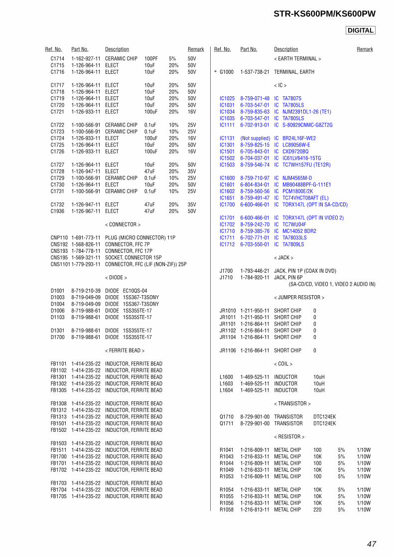
Ref. No. Part No. Description Remark Ref. No. Part No. Description Remark
47
STR-KS600PM/KS600PW
C1714 1-162-927-11 CERAMIC CHIP 100PF 5% 50VC1715 1-126-964-11 ELECT 10uF 20% 50VC1716 1-126-964-11 ELECT 10uF 20% 50V
C1717 1-126-964-11 ELECT 10uF 20% 50VC1718 1-126-964-11 ELECT 10uF 20% 50VC1719 1-126-964-11 ELECT 10uF 20% 50VC1720 1-126-964-11 ELECT 10uF 20% 50VC1721 1-126-933-11 ELECT 100uF 20% 16V
C1722 1-100-566-91 CERAMIC CHIP 0.1uF 10% 25VC1723 1-100-566-91 CERAMIC CHIP 0.1uF 10% 25VC1724 1-126-933-11 ELECT 100uF 20% 16VC1725 1-126-964-11 ELECT 10uF 20% 50VC1726 1-126-933-11 ELECT 100uF 20% 16V
C1727 1-126-964-11 ELECT 10uF 20% 50VC1728 1-126-947-11 ELECT 47uF 20% 35VC1729 1-100-566-91 CERAMIC CHIP 0.1uF 10% 25VC1730 1-126-964-11 ELECT 10uF 20% 50VC1731 1-100-566-91 CERAMIC CHIP 0.1uF 10% 25V
C1732 1-126-947-11 ELECT 47uF 20% 35VC1936 1-126-967-11 ELECT 47uF 20% 50V
< CONNECTOR >
CNP110 1-691-773-11 PLUG (MICRO CONNECTOR) 11PCNS192 1-568-826-11 CONNECTOR, FFC 7PCNS193 1-784-778-11 CONNECTOR, FFC 17PCNS195 1-569-321-11 SOCKET, CONNECTOR 15PCNS1101 1-779-293-11 CONNECTOR, FFC (LIF (NON-ZIF)) 25P
< DIODE >
D1001 8-719-210-39 DIODE EC10QS-04D1003 8-719-049-09 DIODE 1SS367-T3SONYD1004 8-719-049-09 DIODE 1SS367-T3SONYD1006 8-719-988-61 DIODE 1SS355TE-17D1103 8-719-988-61 DIODE 1SS355TE-17
D1301 8-719-988-61 DIODE 1SS355TE-17D1700 8-719-988-61 DIODE 1SS355TE-17
< FERRITE BEAD >
FB1101 1-414-235-22 INDUCTOR, FERRITE BEADFB1102 1-414-235-22 INDUCTOR, FERRITE BEADFB1301 1-414-235-22 INDUCTOR, FERRITE BEADFB1302 1-414-235-22 INDUCTOR, FERRITE BEADFB1305 1-414-235-22 INDUCTOR, FERRITE BEAD
FB1308 1-414-235-22 INDUCTOR, FERRITE BEADFB1312 1-414-235-22 INDUCTOR, FERRITE BEADFB1313 1-414-235-22 INDUCTOR, FERRITE BEADFB1501 1-414-235-22 INDUCTOR, FERRITE BEADFB1502 1-414-235-22 INDUCTOR, FERRITE BEAD
FB1503 1-414-235-22 INDUCTOR, FERRITE BEADFB1511 1-414-235-22 INDUCTOR, FERRITE BEADFB1700 1-414-235-22 INDUCTOR, FERRITE BEADFB1701 1-414-235-22 INDUCTOR, FERRITE BEADFB1702 1-414-235-22 INDUCTOR, FERRITE BEAD
FB1703 1-414-235-22 INDUCTOR, FERRITE BEADFB1704 1-414-235-22 INDUCTOR, FERRITE BEADFB1705 1-414-235-22 INDUCTOR, FERRITE BEAD
< EARTH TERMINAL >
* G1000 1-537-738-21 TERMINAL, EARTH
< IC >
IC1025 8-759-071-48 IC TA7807SIC1031 6-703-547-01 IC TA7805LSIC1034 8-759-835-63 IC NJM2391DL1-26 (TE1)IC1035 6-703-547-01 IC TA7805LSIC1111 6-702-913-01 IC S-80929CNMC-G8ZT2G
IC1131 (Not supplied) IC BR24L16F-WE2IC1301 8-759-825-15 IC LC89056W-EIC1501 6-705-843-01 IC CXD9720BQIC1502 6-704-037-01 IC IC61LV6416-15TGIC1503 8-759-546-74 IC TC7WH157FU (TE12R)
IC1600 8-759-710-97 IC NJM4565M-DIC1601 6-804-834-01 IC MB90488BPF-G-111E1IC1602 8-759-560-56 IC PCM1800E/2KIC1651 8-759-491-47 IC TC74VHCT08AFT (EL)IC1700 6-600-466-01 IC TORX147L (OPT IN SA-CD/CD)
IC1701 6-600-466-01 IC TORX147L (OPT IN VIDEO 2)IC1702 8-759-242-70 IC TC7WU04FIC1710 8-759-385-76 IC MC14052 BDR2IC1711 6-702-771-01 IC TA78033LSIC1712 6-703-550-01 IC TA7809LS
< JACK >
J1700 1-793-446-21 JACK, PIN 1P (COAX IN DVD)J1710 1-784-920-11 JACK, PIN 6P
(SA-CD/CD, VIDEO 1, VIDEO 2 AUDIO IN)
< JUMPER RESISTOR >
JR1010 1-211-950-11 SHORT CHIP 0JR1011 1-211-950-11 SHORT CHIP 0JR1101 1-216-864-11 SHORT CHIP 0JR1102 1-216-864-11 SHORT CHIP 0JR1104 1-216-864-11 SHORT CHIP 0
JR1106 1-216-864-11 SHORT CHIP 0
< COIL >
L1600 1-469-525-11 INDUCTOR 10uHL1603 1-469-525-11 INDUCTOR 10uHL1604 1-469-525-11 INDUCTOR 10uH
< TRANSISTOR >
Q1710 8-729-901-00 TRANSISTOR DTC124EKQ1711 8-729-901-00 TRANSISTOR DTC124EK
< RESISTOR >
R1041 1-216-809-11 METAL CHIP 100 5% 1/10WR1043 1-216-833-11 METAL CHIP 10K 5% 1/10WR1044 1-216-809-11 METAL CHIP 100 5% 1/10WR1049 1-216-833-11 METAL CHIP 10K 5% 1/10WR1053 1-216-809-11 METAL CHIP 100 5% 1/10W
R1054 1-216-833-11 METAL CHIP 10K 5% 1/10WR1055 1-216-833-11 METAL CHIP 10K 5% 1/10WR1056 1-216-833-11 METAL CHIP 10K 5% 1/10WR1058 1-216-813-11 METAL CHIP 220 5% 1/10W
DIGITAL
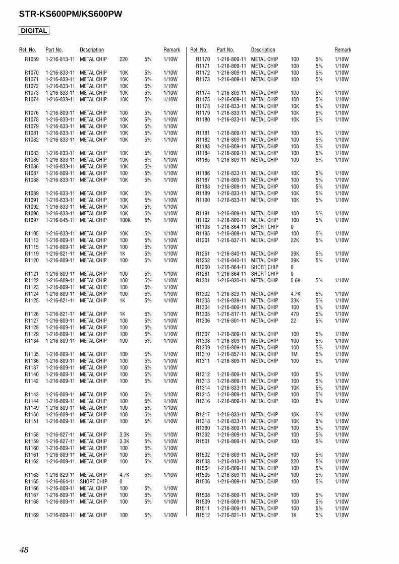
Ref. No. Part No. Description Remark Ref. No. Part No. Description Remark
48
STR-KS600PM/KS600PW
R1059 1-216-813-11 METAL CHIP 220 5% 1/10W
R1070 1-216-833-11 METAL CHIP 10K 5% 1/10WR1071 1-216-833-11 METAL CHIP 10K 5% 1/10WR1072 1-216-833-11 METAL CHIP 10K 5% 1/10WR1073 1-216-833-11 METAL CHIP 10K 5% 1/10WR1074 1-216-833-11 METAL CHIP 10K 5% 1/10W
R1076 1-216-809-11 METAL CHIP 100 5% 1/10WR1078 1-216-833-11 METAL CHIP 10K 5% 1/10WR1079 1-216-833-11 METAL CHIP 10K 5% 1/10WR1081 1-216-833-11 METAL CHIP 10K 5% 1/10WR1082 1-216-833-11 METAL CHIP 10K 5% 1/10W
R1083 1-216-833-11 METAL CHIP 10K 5% 1/10WR1085 1-216-833-11 METAL CHIP 10K 5% 1/10WR1086 1-216-833-11 METAL CHIP 10K 5% 1/10WR1087 1-216-809-11 METAL CHIP 100 5% 1/10WR1088 1-216-833-11 METAL CHIP 10K 5% 1/10W
R1089 1-216-833-11 METAL CHIP 10K 5% 1/10WR1091 1-216-833-11 METAL CHIP 10K 5% 1/10WR1092 1-216-833-11 METAL CHIP 10K 5% 1/10WR1096 1-216-833-11 METAL CHIP 10K 5% 1/10WR1097 1-216-845-11 METAL CHIP 100K 5% 1/10W
R1105 1-216-833-11 METAL CHIP 10K 5% 1/10WR1113 1-216-809-11 METAL CHIP 100 5% 1/10WR1115 1-216-809-11 METAL CHIP 100 5% 1/10WR1119 1-216-821-11 METAL CHIP 1K 5% 1/10WR1120 1-216-809-11 METAL CHIP 100 5% 1/10W
R1121 1-216-809-11 METAL CHIP 100 5% 1/10WR1122 1-216-809-11 METAL CHIP 100 5% 1/10WR1123 1-216-809-11 METAL CHIP 100 5% 1/10WR1124 1-216-809-11 METAL CHIP 100 5% 1/10WR1125 1-216-821-11 METAL CHIP 1K 5% 1/10W
R1126 1-216-821-11 METAL CHIP 1K 5% 1/10WR1127 1-216-809-11 METAL CHIP 100 5% 1/10WR1128 1-216-809-11 METAL CHIP 100 5% 1/10WR1129 1-216-809-11 METAL CHIP 100 5% 1/10WR1134 1-216-809-11 METAL CHIP 100 5% 1/10W
R1135 1-216-809-11 METAL CHIP 100 5% 1/10WR1136 1-216-809-11 METAL CHIP 100 5% 1/10WR1137 1-216-809-11 METAL CHIP 100 5% 1/10WR1140 1-216-809-11 METAL CHIP 100 5% 1/10WR1142 1-216-809-11 METAL CHIP 100 5% 1/10W
R1143 1-216-809-11 METAL CHIP 100 5% 1/10WR1144 1-216-809-11 METAL CHIP 100 5% 1/10WR1149 1-216-809-11 METAL CHIP 100 5% 1/10WR1150 1-216-809-11 METAL CHIP 100 5% 1/10WR1151 1-216-809-11 METAL CHIP 100 5% 1/10W
R1158 1-216-827-11 METAL CHIP 3.3K 5% 1/10WR1159 1-216-827-11 METAL CHIP 3.3K 5% 1/10WR1160 1-216-809-11 METAL CHIP 100 5% 1/10WR1161 1-216-809-11 METAL CHIP 100 5% 1/10WR1162 1-216-809-11 METAL CHIP 100 5% 1/10W
R1163 1-216-829-11 METAL CHIP 4.7K 5% 1/10WR1165 1-216-864-11 SHORT CHIP 0R1166 1-216-809-11 METAL CHIP 100 5% 1/10WR1167 1-216-809-11 METAL CHIP 100 5% 1/10WR1168 1-216-809-11 METAL CHIP 100 5% 1/10W
R1169 1-216-809-11 METAL CHIP 100 5% 1/10W
R1170 1-216-809-11 METAL CHIP 100 5% 1/10WR1171 1-216-809-11 METAL CHIP 100 5% 1/10WR1172 1-216-809-11 METAL CHIP 100 5% 1/10WR1173 1-216-809-11 METAL CHIP 100 5% 1/10W
R1174 1-216-809-11 METAL CHIP 100 5% 1/10WR1175 1-216-809-11 METAL CHIP 100 5% 1/10WR1178 1-216-833-11 METAL CHIP 10K 5% 1/10WR1179 1-216-833-11 METAL CHIP 10K 5% 1/10WR1180 1-216-833-11 METAL CHIP 10K 5% 1/10W
R1181 1-216-809-11 METAL CHIP 100 5% 1/10WR1182 1-216-809-11 METAL CHIP 100 5% 1/10WR1183 1-216-809-11 METAL CHIP 100 5% 1/10WR1184 1-216-809-11 METAL CHIP 100 5% 1/10WR1185 1-216-809-11 METAL CHIP 100 5% 1/10W
R1186 1-216-833-11 METAL CHIP 10K 5% 1/10WR1187 1-216-809-11 METAL CHIP 100 5% 1/10WR1188 1-216-809-11 METAL CHIP 100 5% 1/10WR1189 1-216-833-11 METAL CHIP 10K 5% 1/10WR1190 1-216-833-11 METAL CHIP 10K 5% 1/10W
R1191 1-216-809-11 METAL CHIP 100 5% 1/10WR1192 1-216-809-11 METAL CHIP 100 5% 1/10WR1193 1-216-864-11 SHORT CHIP 0R1195 1-216-809-11 METAL CHIP 100 5% 1/10WR1201 1-216-837-11 METAL CHIP 22K 5% 1/10W
R1251 1-216-840-11 METAL CHIP 39K 5% 1/10WR1252 1-216-840-11 METAL CHIP 39K 5% 1/10WR1260 1-216-864-11 SHORT CHIP 0R1261 1-216-864-11 SHORT CHIP 0R1301 1-216-830-11 METAL CHIP 5.6K 5% 1/10W
R1302 1-216-829-11 METAL CHIP 4.7K 5% 1/10WR1303 1-216-839-11 METAL CHIP 33K 5% 1/10WR1304 1-216-809-11 METAL CHIP 100 5% 1/10WR1305 1-216-817-11 METAL CHIP 470 5% 1/10WR1306 1-216-801-11 METAL CHIP 22 5% 1/10W
R1307 1-216-809-11 METAL CHIP 100 5% 1/10WR1308 1-216-809-11 METAL CHIP 100 5% 1/10WR1309 1-216-809-11 METAL CHIP 100 5% 1/10WR1310 1-216-857-11 METAL CHIP 1M 5% 1/10WR1311 1-216-809-11 METAL CHIP 100 5% 1/10W
R1312 1-216-809-11 METAL CHIP 100 5% 1/10WR1313 1-216-809-11 METAL CHIP 100 5% 1/10WR1314 1-216-833-11 METAL CHIP 10K 5% 1/10WR1315 1-216-809-11 METAL CHIP 100 5% 1/10WR1316 1-216-809-11 METAL CHIP 100 5% 1/10W
R1317 1-216-833-11 METAL CHIP 10K 5% 1/10WR1318 1-216-833-11 METAL CHIP 10K 5% 1/10WR1360 1-216-809-11 METAL CHIP 100 5% 1/10WR1362 1-216-809-11 METAL CHIP 100 5% 1/10WR1501 1-216-809-11 METAL CHIP 100 5% 1/10W
R1502 1-216-809-11 METAL CHIP 100 5% 1/10WR1503 1-216-813-11 METAL CHIP 220 5% 1/10WR1504 1-216-809-11 METAL CHIP 100 5% 1/10WR1505 1-216-809-11 METAL CHIP 100 5% 1/10WR1506 1-216-809-11 METAL CHIP 100 5% 1/10W
R1508 1-216-809-11 METAL CHIP 100 5% 1/10WR1509 1-216-809-11 METAL CHIP 100 5% 1/10WR1511 1-216-809-11 METAL CHIP 100 5% 1/10WR1512 1-216-821-11 METAL CHIP 1K 5% 1/10W
DIGITAL
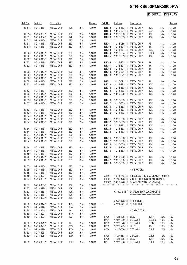
Ref. No. Part No. Description Remark Ref. No. Part No. Description Remark
49
STR-KS600PM/KS600PW
R1513 1-216-833-11 METAL CHIP 10K 5% 1/10W
R1514 1-216-833-11 METAL CHIP 10K 5% 1/10WR1515 1-216-857-11 METAL CHIP 1M 5% 1/10WR1517 1-216-813-11 METAL CHIP 220 5% 1/10WR1518 1-216-813-11 METAL CHIP 220 5% 1/10WR1519 1-216-813-11 METAL CHIP 220 5% 1/10W
R1520 1-216-813-11 METAL CHIP 220 5% 1/10WR1521 1-216-813-11 METAL CHIP 220 5% 1/10WR1522 1-216-813-11 METAL CHIP 220 5% 1/10WR1523 1-216-813-11 METAL CHIP 220 5% 1/10WR1525 1-216-813-11 METAL CHIP 220 5% 1/10W
R1526 1-216-813-11 METAL CHIP 220 5% 1/10WR1527 1-216-813-11 METAL CHIP 220 5% 1/10WR1528 1-216-813-11 METAL CHIP 220 5% 1/10WR1529 1-216-813-11 METAL CHIP 220 5% 1/10WR1532 1-216-813-11 METAL CHIP 220 5% 1/10W
R1533 1-216-813-11 METAL CHIP 220 5% 1/10WR1534 1-216-813-11 METAL CHIP 220 5% 1/10WR1535 1-216-813-11 METAL CHIP 220 5% 1/10WR1536 1-216-813-11 METAL CHIP 220 5% 1/10WR1537 1-216-813-11 METAL CHIP 220 5% 1/10W
R1538 1-216-813-11 METAL CHIP 220 5% 1/10WR1539 1-216-813-11 METAL CHIP 220 5% 1/10WR1540 1-216-813-11 METAL CHIP 220 5% 1/10WR1541 1-216-813-11 METAL CHIP 220 5% 1/10WR1542 1-216-813-11 METAL CHIP 220 5% 1/10W
R1543 1-216-813-11 METAL CHIP 220 5% 1/10WR1544 1-216-813-11 METAL CHIP 220 5% 1/10WR1545 1-216-813-11 METAL CHIP 220 5% 1/10WR1546 1-216-813-11 METAL CHIP 220 5% 1/10WR1547 1-216-813-11 METAL CHIP 220 5% 1/10W
R1548 1-216-813-11 METAL CHIP 220 5% 1/10WR1549 1-216-813-11 METAL CHIP 220 5% 1/10WR1550 1-216-813-11 METAL CHIP 220 5% 1/10WR1551 1-216-813-11 METAL CHIP 220 5% 1/10WR1552 1-216-813-11 METAL CHIP 220 5% 1/10W
R1553 1-216-813-11 METAL CHIP 220 5% 1/10WR1554 1-216-813-11 METAL CHIP 220 5% 1/10WR1555 1-216-813-11 METAL CHIP 220 5% 1/10WR1556 1-216-809-11 METAL CHIP 100 5% 1/10WR1570 1-216-833-11 METAL CHIP 10K 5% 1/10W
R1571 1-216-833-11 METAL CHIP 10K 5% 1/10WR1572 1-216-833-11 METAL CHIP 10K 5% 1/10WR1573 1-216-833-11 METAL CHIP 10K 5% 1/10WR1574 1-216-833-11 METAL CHIP 10K 5% 1/10WR1601 1-216-833-11 METAL CHIP 10K 5% 1/10W
R1602 1-216-817-11 METAL CHIP 470 5% 1/10WR1603 1-216-827-11 METAL CHIP 3.3K 5% 1/10WR1604 1-216-821-11 METAL CHIP 1K 5% 1/10WR1605 1-216-829-11 METAL CHIP 4.7K 5% 1/10WR1606 1-216-809-11 METAL CHIP 100 5% 1/10W
R1607 1-216-821-11 METAL CHIP 1K 5% 1/10WR1608 1-216-825-11 METAL CHIP 2.2K 5% 1/10WR1610 1-216-829-11 METAL CHIP 4.7K 5% 1/10WR1635 1-216-825-11 METAL CHIP 2.2K 5% 1/10WR1636 1-216-825-11 METAL CHIP 2.2K 5% 1/10W
R1651 1-216-833-11 METAL CHIP 10K 5% 1/10W
R1652 1-216-833-11 METAL CHIP 10K 5% 1/10WR1653 1-216-827-11 METAL CHIP 3.3K 5% 1/10WR1654 1-216-833-11 METAL CHIP 10K 5% 1/10WR1700 1-216-809-11 METAL CHIP 100 5% 1/10W
R1701 1-218-285-11 METAL CHIP 75 5% 1/10WR1702 1-216-821-11 METAL CHIP 1K 5% 1/10WR1703 1-216-837-11 METAL CHIP 22K 5% 1/10WR1704 1-216-854-11 METAL CHIP 560K 5% 1/10WR1705 1-216-809-11 METAL CHIP 100 5% 1/10W
R1706 1-216-821-11 METAL CHIP 1K 5% 1/10WR1707 1-216-821-11 METAL CHIP 1K 5% 1/10WR1708 1-216-821-11 METAL CHIP 1K 5% 1/10WR1709 1-216-821-11 METAL CHIP 1K 5% 1/10WR1710 1-216-821-11 METAL CHIP 1K 5% 1/10W
R1711 1-216-821-11 METAL CHIP 1K 5% 1/10WR1712 1-216-833-11 METAL CHIP 10K 5% 1/10WR1713 1-216-833-11 METAL CHIP 10K 5% 1/10WR1714 1-216-833-11 METAL CHIP 10K 5% 1/10WR1715 1-216-833-11 METAL CHIP 10K 5% 1/10W
R1716 1-216-833-11 METAL CHIP 10K 5% 1/10WR1717 1-216-833-11 METAL CHIP 10K 5% 1/10WR1718 1-216-833-11 METAL CHIP 10K 5% 1/10WR1719 1-216-833-11 METAL CHIP 10K 5% 1/10WR1720 1-216-833-11 METAL CHIP 10K 5% 1/10W
R1721 1-216-833-11 METAL CHIP 10K 5% 1/10WR1722 1-216-833-11 METAL CHIP 10K 5% 1/10WR1723 1-216-833-11 METAL CHIP 10K 5% 1/10WR1724 1-216-833-11 METAL CHIP 10K 5% 1/10WR1725 1-216-833-11 METAL CHIP 10K 5% 1/10W
R1726 1-216-833-11 METAL CHIP 10K 5% 1/10WR1727 1-216-833-11 METAL CHIP 10K 5% 1/10WR1728 1-216-809-11 METAL CHIP 100 5% 1/10WR1729 1-216-809-11 METAL CHIP 100 5% 1/10WR1730 1-216-833-11 METAL CHIP 10K 5% 1/10W
R1731 1-216-833-11 METAL CHIP 10K 5% 1/10WR1732 1-216-833-11 METAL CHIP 10K 5% 1/10WR1733 1-216-833-11 METAL CHIP 10K 5% 1/10W
< VIBRATOR >
X1101 1-813-448-21 PIEZOELECTRIC OSCILLATOR (24MHz)X1301 1-795-126-21 VIBRATOR, CRYSTAL (12.288MHz)X1502 1-813-276-21 QUARTZ CRYSTAL (13.9MHz)
************************************************************
A-1097-936-A DISPLAY BOARD, COMPLETE************************
4-246-476-01 HOLDER (FL)* 4-921-941-01 CUSHION (FL)
< CAPACITOR >
C700 1-126-795-11 ELECT 10uF 20% 50VC701 1-127-880-11 CERAMIC 0.022uF 10% 50VC702 1-127-876-11 CERAMIC 0.01uF 10% 50VC703 1-126-795-11 ELECT 10uF 20% 50VC704 1-127-888-11 CERAMIC 0.1uF 10% 50V
C705 1-127-888-11 CERAMIC 0.1uF 10% 50VC706 1-126-795-11 ELECT 10uF 20% 50VC707 1-127-888-11 CERAMIC 0.1uF 10% 50V
DIGITAL DISPLAY
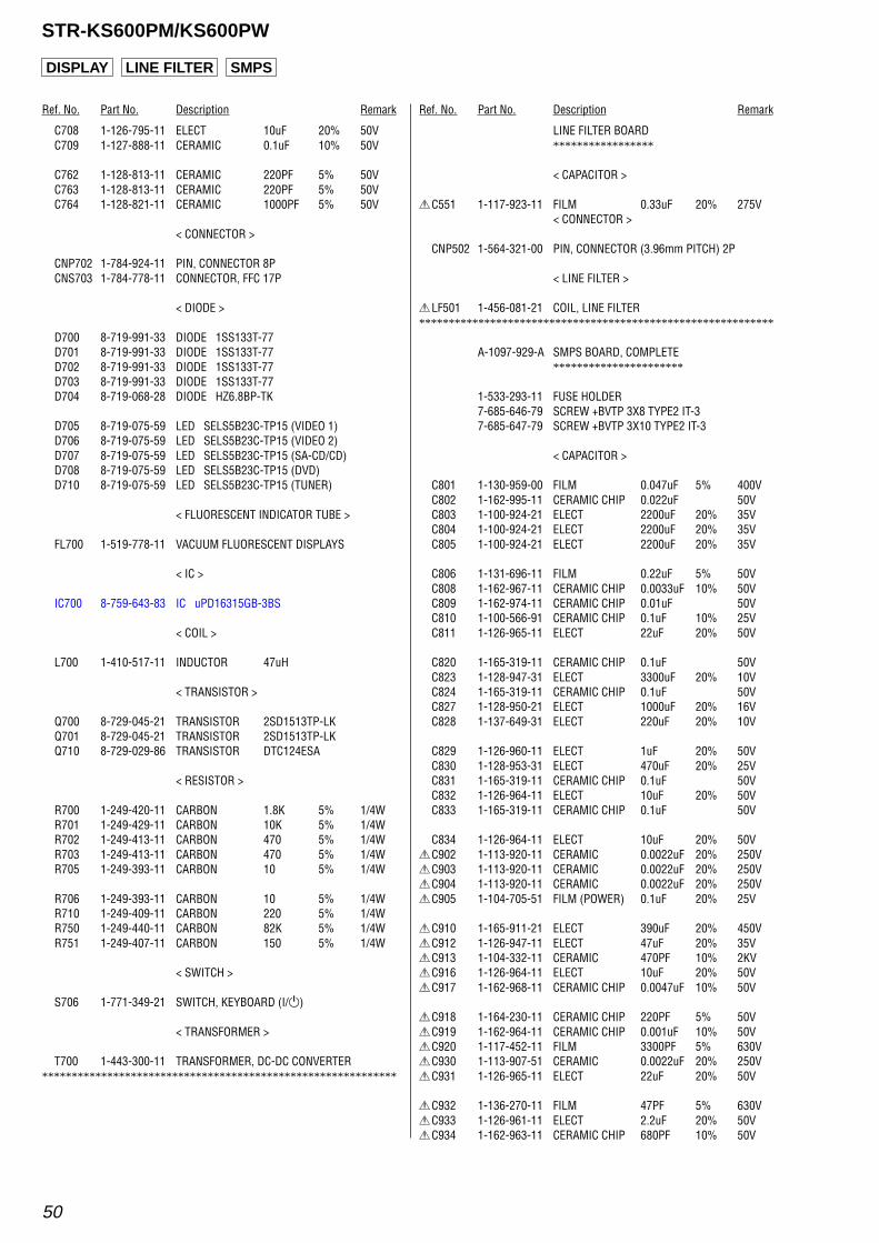
Ref. No. Part No. Description Remark Ref. No. Part No. Description Remark
50
STR-KS600PM/KS600PW
C708 1-126-795-11 ELECT 10uF 20% 50VC709 1-127-888-11 CERAMIC 0.1uF 10% 50V
C762 1-128-813-11 CERAMIC 220PF 5% 50VC763 1-128-813-11 CERAMIC 220PF 5% 50VC764 1-128-821-11 CERAMIC 1000PF 5% 50V
< CONNECTOR >
CNP702 1-784-924-11 PIN, CONNECTOR 8PCNS703 1-784-778-11 CONNECTOR, FFC 17P
< DIODE >
D700 8-719-991-33 DIODE 1SS133T-77D701 8-719-991-33 DIODE 1SS133T-77D702 8-719-991-33 DIODE 1SS133T-77D703 8-719-991-33 DIODE 1SS133T-77D704 8-719-068-28 DIODE HZ6.8BP-TK
D705 8-719-075-59 LED SELS5B23C-TP15 (VIDEO 1)D706 8-719-075-59 LED SELS5B23C-TP15 (VIDEO 2)D707 8-719-075-59 LED SELS5B23C-TP15 (SA-CD/CD)D708 8-719-075-59 LED SELS5B23C-TP15 (DVD)D710 8-719-075-59 LED SELS5B23C-TP15 (TUNER)
< FLUORESCENT INDICATOR TUBE >
FL700 1-519-778-11 VACUUM FLUORESCENT DISPLAYS
< IC >
IC700 8-759-643-83 IC uPD16315GB-3BS
< COIL >
L700 1-410-517-11 INDUCTOR 47uH
< TRANSISTOR >
Q700 8-729-045-21 TRANSISTOR 2SD1513TP-LKQ701 8-729-045-21 TRANSISTOR 2SD1513TP-LKQ710 8-729-029-86 TRANSISTOR DTC124ESA
< RESISTOR >
R700 1-249-420-11 CARBON 1.8K 5% 1/4WR701 1-249-429-11 CARBON 10K 5% 1/4WR702 1-249-413-11 CARBON 470 5% 1/4WR703 1-249-413-11 CARBON 470 5% 1/4WR705 1-249-393-11 CARBON 10 5% 1/4W
R706 1-249-393-11 CARBON 10 5% 1/4WR710 1-249-409-11 CARBON 220 5% 1/4WR750 1-249-440-11 CARBON 82K 5% 1/4WR751 1-249-407-11 CARBON 150 5% 1/4W
< SWITCH >
S706 1-771-349-21 SWITCH, KEYBOARD (I/1)
< TRANSFORMER >
T700 1-443-300-11 TRANSFORMER, DC-DC CONVERTER************************************************************
LINE FILTER BOARD*****************
< CAPACITOR >
0C551 1-117-923-11 FILM 0.33uF 20% 275V< CONNECTOR >
CNP502 1-564-321-00 PIN, CONNECTOR (3.96mm PITCH) 2P
< LINE FILTER >
0LF501 1-456-081-21 COIL, LINE FILTER************************************************************
A-1097-929-A SMPS BOARD, COMPLETE**********************
1-533-293-11 FUSE HOLDER7-685-646-79 SCREW +BVTP 3X8 TYPE2 IT-37-685-647-79 SCREW +BVTP 3X10 TYPE2 IT-3
< CAPACITOR >
C801 1-130-959-00 FILM 0.047uF 5% 400VC802 1-162-995-11 CERAMIC CHIP 0.022uF 50VC803 1-100-924-21 ELECT 2200uF 20% 35VC804 1-100-924-21 ELECT 2200uF 20% 35VC805 1-100-924-21 ELECT 2200uF 20% 35V
C806 1-131-696-11 FILM 0.22uF 5% 50VC808 1-162-967-11 CERAMIC CHIP 0.0033uF 10% 50VC809 1-162-974-11 CERAMIC CHIP 0.01uF 50VC810 1-100-566-91 CERAMIC CHIP 0.1uF 10% 25VC811 1-126-965-11 ELECT 22uF 20% 50V
C820 1-165-319-11 CERAMIC CHIP 0.1uF 50VC823 1-128-947-31 ELECT 3300uF 20% 10VC824 1-165-319-11 CERAMIC CHIP 0.1uF 50VC827 1-128-950-21 ELECT 1000uF 20% 16VC828 1-137-649-31 ELECT 220uF 20% 10V
C829 1-126-960-11 ELECT 1uF 20% 50VC830 1-128-953-31 ELECT 470uF 20% 25VC831 1-165-319-11 CERAMIC CHIP 0.1uF 50VC832 1-126-964-11 ELECT 10uF 20% 50VC833 1-165-319-11 CERAMIC CHIP 0.1uF 50V
C834 1-126-964-11 ELECT 10uF 20% 50V0C902 1-113-920-11 CERAMIC 0.0022uF 20% 250V0C903 1-113-920-11 CERAMIC 0.0022uF 20% 250V0C904 1-113-920-11 CERAMIC 0.0022uF 20% 250V0C905 1-104-705-51 FILM (POWER) 0.1uF 20% 25V
0C910 1-165-911-21 ELECT 390uF 20% 450V0C912 1-126-947-11 ELECT 47uF 20% 35V0C913 1-104-332-11 CERAMIC 470PF 10% 2KV0C916 1-126-964-11 ELECT 10uF 20% 50V0C917 1-162-968-11 CERAMIC CHIP 0.0047uF 10% 50V
0C918 1-164-230-11 CERAMIC CHIP 220PF 5% 50V0C919 1-162-964-11 CERAMIC CHIP 0.001uF 10% 50V0C920 1-117-452-11 FILM 3300PF 5% 630V0C930 1-113-907-51 CERAMIC 0.0022uF 20% 250V0C931 1-126-965-11 ELECT 22uF 20% 50V
0C932 1-136-270-11 FILM 47PF 5% 630V0C933 1-126-961-11 ELECT 2.2uF 20% 50V0C934 1-162-963-11 CERAMIC CHIP 680PF 10% 50V
DISPLAY LINE FILTER SMPS
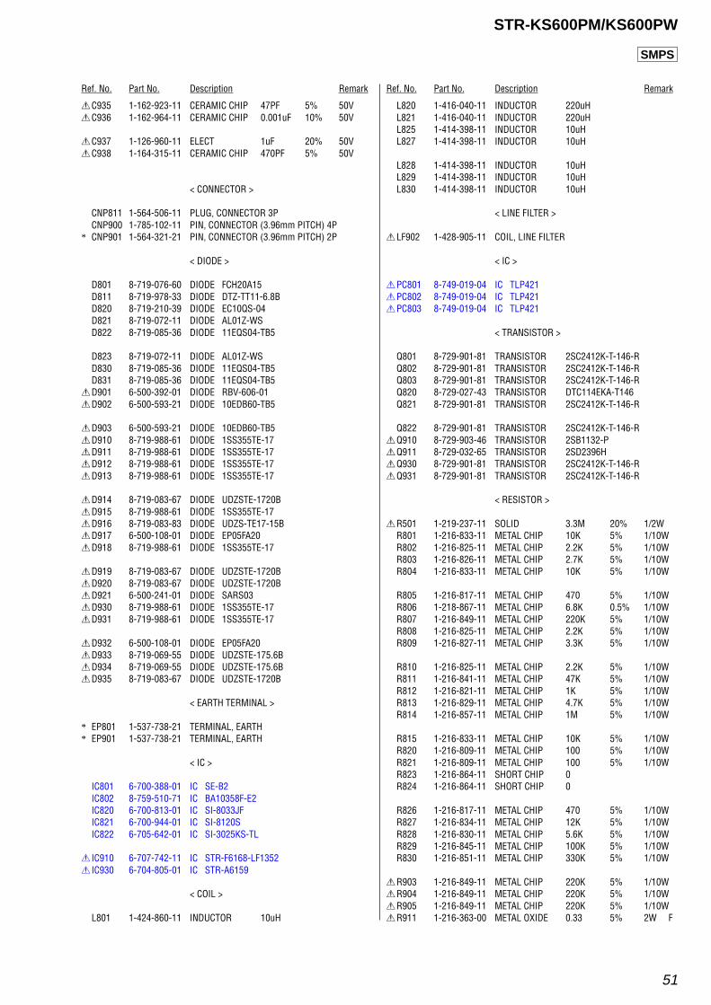
Ref. No. Part No. Description Remark Ref. No. Part No. Description Remark
51
STR-KS600PM/KS600PW
0C935 1-162-923-11 CERAMIC CHIP 47PF 5% 50V0C936 1-162-964-11 CERAMIC CHIP 0.001uF 10% 50V
0C937 1-126-960-11 ELECT 1uF 20% 50V0C938 1-164-315-11 CERAMIC CHIP 470PF 5% 50V
< CONNECTOR >
CNP811 1-564-506-11 PLUG, CONNECTOR 3PCNP900 1-785-102-11 PIN, CONNECTOR (3.96mm PITCH) 4P
* CNP901 1-564-321-21 PIN, CONNECTOR (3.96mm PITCH) 2P
< DIODE >
D801 8-719-076-60 DIODE FCH20A15D811 8-719-978-33 DIODE DTZ-TT11-6.8BD820 8-719-210-39 DIODE EC10QS-04D821 8-719-072-11 DIODE AL01Z-WSD822 8-719-085-36 DIODE 11EQS04-TB5
D823 8-719-072-11 DIODE AL01Z-WSD830 8-719-085-36 DIODE 11EQS04-TB5D831 8-719-085-36 DIODE 11EQS04-TB5
0D901 6-500-392-01 DIODE RBV-606-010D902 6-500-593-21 DIODE 10EDB60-TB5
0D903 6-500-593-21 DIODE 10EDB60-TB50D910 8-719-988-61 DIODE 1SS355TE-170D911 8-719-988-61 DIODE 1SS355TE-170D912 8-719-988-61 DIODE 1SS355TE-170D913 8-719-988-61 DIODE 1SS355TE-17
0D914 8-719-083-67 DIODE UDZSTE-1720B0D915 8-719-988-61 DIODE 1SS355TE-170D916 8-719-083-83 DIODE UDZS-TE17-15B0D917 6-500-108-01 DIODE EP05FA200D918 8-719-988-61 DIODE 1SS355TE-17
0D919 8-719-083-67 DIODE UDZSTE-1720B0D920 8-719-083-67 DIODE UDZSTE-1720B0D921 6-500-241-01 DIODE SARS030D930 8-719-988-61 DIODE 1SS355TE-170D931 8-719-988-61 DIODE 1SS355TE-17
0D932 6-500-108-01 DIODE EP05FA200D933 8-719-069-55 DIODE UDZSTE-175.6B0D934 8-719-069-55 DIODE UDZSTE-175.6B0D935 8-719-083-67 DIODE UDZSTE-1720B
< EARTH TERMINAL >
* EP801 1-537-738-21 TERMINAL, EARTH* EP901 1-537-738-21 TERMINAL, EARTH
< IC >
IC801 6-700-388-01 IC SE-B2IC802 8-759-510-71 IC BA10358F-E2IC820 6-700-813-01 IC SI-8033JFIC821 6-700-944-01 IC SI-8120SIC822 6-705-642-01 IC SI-3025KS-TL
0 IC910 6-707-742-11 IC STR-F6168-LF13520 IC930 6-704-805-01 IC STR-A6159
< COIL >
L801 1-424-860-11 INDUCTOR 10uH
L820 1-416-040-11 INDUCTOR 220uHL821 1-416-040-11 INDUCTOR 220uHL825 1-414-398-11 INDUCTOR 10uHL827 1-414-398-11 INDUCTOR 10uH
L828 1-414-398-11 INDUCTOR 10uHL829 1-414-398-11 INDUCTOR 10uHL830 1-414-398-11 INDUCTOR 10uH
< LINE FILTER >
0LF902 1-428-905-11 COIL, LINE FILTER
< IC >
0PC801 8-749-019-04 IC TLP4210PC802 8-749-019-04 IC TLP4210PC803 8-749-019-04 IC TLP421
< TRANSISTOR >
Q801 8-729-901-81 TRANSISTOR 2SC2412K-T-146-RQ802 8-729-901-81 TRANSISTOR 2SC2412K-T-146-RQ803 8-729-901-81 TRANSISTOR 2SC2412K-T-146-RQ820 8-729-027-43 TRANSISTOR DTC114EKA-T146Q821 8-729-901-81 TRANSISTOR 2SC2412K-T-146-R
Q822 8-729-901-81 TRANSISTOR 2SC2412K-T-146-R0Q910 8-729-903-46 TRANSISTOR 2SB1132-P0Q911 8-729-032-65 TRANSISTOR 2SD2396H0Q930 8-729-901-81 TRANSISTOR 2SC2412K-T-146-R0Q931 8-729-901-81 TRANSISTOR 2SC2412K-T-146-R
< RESISTOR >
0R501 1-219-237-11 SOLID 3.3M 20% 1/2WR801 1-216-833-11 METAL CHIP 10K 5% 1/10WR802 1-216-825-11 METAL CHIP 2.2K 5% 1/10WR803 1-216-826-11 METAL CHIP 2.7K 5% 1/10WR804 1-216-833-11 METAL CHIP 10K 5% 1/10W
R805 1-216-817-11 METAL CHIP 470 5% 1/10WR806 1-218-867-11 METAL CHIP 6.8K 0.5% 1/10WR807 1-216-849-11 METAL CHIP 220K 5% 1/10WR808 1-216-825-11 METAL CHIP 2.2K 5% 1/10WR809 1-216-827-11 METAL CHIP 3.3K 5% 1/10W
R810 1-216-825-11 METAL CHIP 2.2K 5% 1/10WR811 1-216-841-11 METAL CHIP 47K 5% 1/10WR812 1-216-821-11 METAL CHIP 1K 5% 1/10WR813 1-216-829-11 METAL CHIP 4.7K 5% 1/10WR814 1-216-857-11 METAL CHIP 1M 5% 1/10W
R815 1-216-833-11 METAL CHIP 10K 5% 1/10WR820 1-216-809-11 METAL CHIP 100 5% 1/10WR821 1-216-809-11 METAL CHIP 100 5% 1/10WR823 1-216-864-11 SHORT CHIP 0R824 1-216-864-11 SHORT CHIP 0
R826 1-216-817-11 METAL CHIP 470 5% 1/10WR827 1-216-834-11 METAL CHIP 12K 5% 1/10WR828 1-216-830-11 METAL CHIP 5.6K 5% 1/10WR829 1-216-845-11 METAL CHIP 100K 5% 1/10WR830 1-216-851-11 METAL CHIP 330K 5% 1/10W
0R903 1-216-849-11 METAL CHIP 220K 5% 1/10W0R904 1-216-849-11 METAL CHIP 220K 5% 1/10W0R905 1-216-849-11 METAL CHIP 220K 5% 1/10W0R911 1-216-363-00 METAL OXIDE 0.33 5% 2W F
SMPS
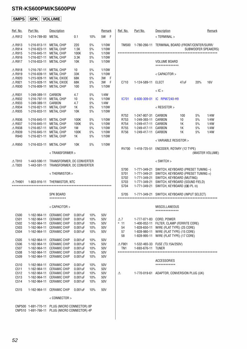
Ref. No. Part No. Description Remark Ref. No. Part No. Description Remark
52
STR-KS600PM/KS600PW
0R912 1-214-789-00 METAL 0.1 10% 5W F
0R913 1-216-813-11 METAL CHIP 220 5% 1/10W0R914 1-216-823-11 METAL CHIP 1.5K 5% 1/10W0R915 1-216-845-11 METAL CHIP 100K 5% 1/10W0R916 1-216-827-11 METAL CHIP 3.3K 5% 1/10W0R917 1-216-833-11 METAL CHIP 10K 5% 1/10W
0R918 1-216-797-11 METAL CHIP 10 5% 1/10W0R919 1-216-839-11 METAL CHIP 33K 5% 1/10W0R920 1-215-928-11 METAL OXIDE 68K 5% 3W F0R921 1-215-928-11 METAL OXIDE 68K 5% 3W F0R930 1-216-809-11 METAL CHIP 100 5% 1/10W
0R931 1-249-389-11 CARBON 4.7 5% 1/4W0R932 1-216-797-11 METAL CHIP 10 5% 1/10W0R933 1-249-389-11 CARBON 4.7 5% 1/4W0R934 1-216-821-11 METAL CHIP 1K 5% 1/10W0R935 1-216-833-11 METAL CHIP 10K 5% 1/10W
0R936 1-216-845-11 METAL CHIP 100K 5% 1/10W0R937 1-216-845-11 METAL CHIP 100K 5% 1/10W0R938 1-216-857-11 METAL CHIP 1M 5% 1/10W0R939 1-216-845-11 METAL CHIP 100K 5% 1/10W
R940 1-216-821-11 METAL CHIP 1K 5% 1/10W
0R950 1-216-833-11 METAL CHIP 10K 5% 1/10W
< TRANSFORMER >
0T910 1-443-590-11 TRANSFORMER, DC CONVERTER0T920 1-443-591-11 TRANSFORMER, DC CONVERTER
< THERMISTOR >
0TH901 1-803-916-11 THERMISTOR, NTC************************************************************
SPK BOARD**********
< CAPACITOR >
C500 1-162-964-11 CERAMIC CHIP 0.001uF 10% 50VC501 1-162-964-11 CERAMIC CHIP 0.001uF 10% 50VC502 1-162-964-11 CERAMIC CHIP 0.001uF 10% 50VC503 1-162-964-11 CERAMIC CHIP 0.001uF 10% 50VC504 1-162-964-11 CERAMIC CHIP 0.001uF 10% 50V
C505 1-162-964-11 CERAMIC CHIP 0.001uF 10% 50VC506 1-162-964-11 CERAMIC CHIP 0.001uF 10% 50VC507 1-162-964-11 CERAMIC CHIP 0.001uF 10% 50VC508 1-162-964-11 CERAMIC CHIP 0.001uF 10% 50VC509 1-162-964-11 CERAMIC CHIP 0.001uF 10% 50V
C510 1-162-964-11 CERAMIC CHIP 0.001uF 10% 50VC511 1-162-964-11 CERAMIC CHIP 0.001uF 10% 50VC512 1-162-964-11 CERAMIC CHIP 0.001uF 10% 50VC513 1-162-964-11 CERAMIC CHIP 0.001uF 10% 50VC514 1-162-964-11 CERAMIC CHIP 0.001uF 10% 50V
C515 1-162-964-11 CERAMIC CHIP 0.001uF 10% 50V
< CONNECTOR >
CNP500 1-691-770-11 PLUG (MICRO CONNECTOR) 8PCNP510 1-691-766-11 PLUG (MICRO CONNECTOR) 4P
< TERMINAL >
TM500 1-780-266-11 TERMINAL BOARD (FRONT/CENTER/SURR/SUBWOOFER SPEAKERS)
************************************************************
VOLUME BOARD**************
< CAPACITOR >
C710 1-124-589-11 ELECT 47uF 20% 16V
< IC >
IC701 6-600-309-01 IC RPM7240-H9
< RESISTOR >
R752 1-247-807-31 CARBON 100 5% 1/4WR753 1-249-393-11 CARBON 10 5% 1/4WR754 1-249-417-11 CARBON 1K 5% 1/4WR755 1-249-417-11 CARBON 1K 5% 1/4WR756 1-249-417-11 CARBON 1K 5% 1/4W
< VARIABLE RESISTOR >
RV700 1-418-725-51 ENCODER, ROTARY (12 TYPE)(MASTER VOLUME)
< SWITCH >
S700 1-771-349-21 SWITCH, KEYBOARD (PRESET TUNING –)S701 1-771-349-21 SWITCH, KEYBOARD (PRESET TUNING +)S702 1-771-349-21 SWITCH, KEYBOARD (MUTING)S703 1-771-349-21 SWITCH, KEYBOARD (SOUND FIELD)S704 1-771-349-21 SWITCH, KEYBOARD (; PL II)
S705 1-771-349-21 SWITCH, KEYBOARD (INPUT SELECT)************************************************************
MISCELLANEOUS**************
07 1-777-071-83 CORD, POWER* 11 1-400-052-11 FILTER, CLAMP (FERRITE CORE)
54 1-828-650-11 WIRE (FLAT TYPE) (25 CORE)57 1-828-980-11 WIRE (FLAT TYPE) (15 CORE)58 1-828-995-11 WIRE (FLAT TYPE) (17 CORE)
0F901 1-532-465-33 FUSE (T3.15A/250V)TN1 1-693-676-11 TUNER
************************************************************
ACCESSORIES************
0 1-770-019-61 ADAPTOR, CONVERSION PLUG (UK)
SMPS SPK VOLUME

53
STR-KS600PM/KS600PW
MEMO
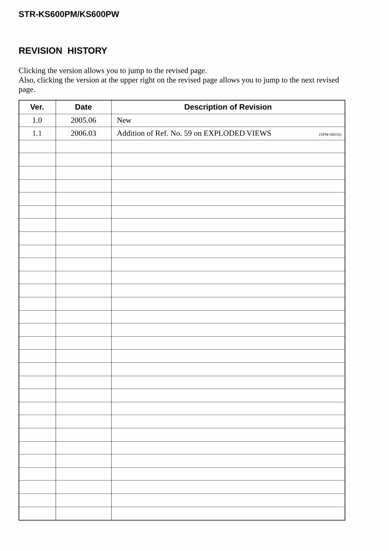
2
STR-KS600PM/KS600PW
REVISION HISTORY
Clicking the version allows you to jump to the revised page.Also, clicking the version at the upper right on the revised page allows you to jump to the next revisedpage.
Ver. Date Description of Revision
1.0 2005.06 New
1.1 2006.03 Addition of Ref. No. 59 on EXPLODED VIEWS (SPM-06016)
Related Documents