arXiv:1006.5472v2 [cond-mat.mtrl-sci] 1 Jul 2010 STM and RHEED study of the Si(001)-c (8 × 8) surface Larisa V. Arapkina * , Vladimir M. Shevlyuga, Vladimir A. Yuryev * A.M.Prokhorov General Physics Institute of the Russian Academy of Sciences, 38 Vavilov Street, Moscow, 119991, Russia Abstract The Si(001) surface deoxidized by short annealing at T ∼ 925 ◦ C in the ultrahigh vacuum molecular beam epitaxy chamber has been in situ investigated by high res- olution scanning tunnelling microscopy (STM) and reflected high energy electron diffraction (RHEED). RHEED patterns corresponding to (2 × 1) and (4 × 4) struc- tures were observed during sample treatment. The (4 × 4) reconstruction arose at T 600 ◦ C after annealing. The reconstruction was observed to be reversible: the (4 × 4) structure turned into the (2 × 1) one at T 600 ◦ C, the (4 × 4) structure ap- peared again at recurring cooling. The c(8 × 8) reconstruction was revealed by STM at room temperature on the same samples. A fraction of the surface area covered by the c(8 × 8) structure decreased as the sample cooling rate was reduced. The (2 × 1) structure was observed on the surface free of the c(8 × 8) one. The c(8 × 8) structure has been evidenced to manifest itself as the (4 × 4) one in the RHEED patterns. A model of the c(8 × 8) structure formation has been built on the basis of the STM data. Origin of the high-order structure on the Si(001) surface and its connection with the epinucleation phenomenon are discussed. Key words: Silicon, Surface reconstruction, Scanning tunnelling microscopy, Reflected high energy electron diffraction PACS: 68.35.B-, 68.37.Ef, 68.49.Jk, 68.47.Fg * Corresponding author. Email addresses: [email protected] (Larisa V. Arapkina), [email protected] (Vladimir A. Yuryev). URL: www.gpi.ru/eng/staff s.php?eng=1&id=125 (Vladimir A. Yuryev). Preprint submitted to Elsevier 14 March 2013

Welcome message from author
This document is posted to help you gain knowledge. Please leave a comment to let me know what you think about it! Share it to your friends and learn new things together.
Transcript
arX
iv:1
006.
5472
v2 [
cond
-mat
.mtr
l-sc
i] 1
Jul
201
0
STM and RHEED study of the
Si(001)-c(8× 8) surface
Larisa V. Arapkina ∗, Vladimir M. Shevlyuga,
Vladimir A. Yuryev ∗
A.M.Prokhorov General Physics Institute of the Russian Academy of Sciences,
38 Vavilov Street, Moscow, 119991, Russia
Abstract
The Si(001) surface deoxidized by short annealing at T ∼ 925C in the ultrahighvacuum molecular beam epitaxy chamber has been in situ investigated by high res-olution scanning tunnelling microscopy (STM) and reflected high energy electrondiffraction (RHEED). RHEED patterns corresponding to (2× 1) and (4× 4) struc-tures were observed during sample treatment. The (4 × 4) reconstruction arose atT . 600C after annealing. The reconstruction was observed to be reversible: the(4× 4) structure turned into the (2× 1) one at T & 600C, the (4× 4) structure ap-peared again at recurring cooling. The c(8×8) reconstruction was revealed by STMat room temperature on the same samples. A fraction of the surface area coveredby the c(8 × 8) structure decreased as the sample cooling rate was reduced. The(2× 1) structure was observed on the surface free of the c(8× 8) one. The c(8× 8)structure has been evidenced to manifest itself as the (4 × 4) one in the RHEEDpatterns. A model of the c(8 × 8) structure formation has been built on the basisof the STM data. Origin of the high-order structure on the Si(001) surface and itsconnection with the epinucleation phenomenon are discussed.
Key words: Silicon, Surface reconstruction, Scanning tunnelling microscopy,Reflected high energy electron diffractionPACS: 68.35.B-, 68.37.Ef, 68.49.Jk, 68.47.Fg
∗ Corresponding author.Email addresses: [email protected] (Larisa V. Arapkina),
[email protected] (Vladimir A. Yuryev).URL: www.gpi.ru/eng/staff s.php?eng=1&id=125 (Vladimir A. Yuryev).
Preprint submitted to Elsevier 14 March 2013
1 Introduction
Investigations of clean silicon surfaces prepared in conditions of actual tech-nological chambers are of great interest due to the industrial requirements tooperate on nanometer and subnanometer scale when designing future nano-electronic devices [1]. In the nearest future, the sizes of structural elements ofsuch devices will be close to the dimensions of structure features of Si(001)surface, at least of its high-order reconstructions such as c(8 × 8). Most ofresearches of the Si(001) surface have thus far been carried out in speciallyrefined conditions which allowed one to study the most common types ofthe surface reconstructions such as (2 × 1), c(4 × 4), c(4 × 2) or c(8 × 8)[2,3,4,5,6,7,8,9,10,11,12,13,14]. Unfortunately, no or very few papers have thusfar been devoted to investigations of the Si surface which is formed as a resultof the wafer cleaning and deoxidation directly in the device manufacturingequipment [14]. But anyone who deals with Si-based nanostructure engineer-ing and the development of such nanostructure formation cycles compatiblewith some standard device manufacturing processes meets the challengingproblem of obtaining the clean Si surface within the imposed technologicalrestrictions which is one of the key elements of the entire structure formationcycle [1,15,16].
The case is that the ambient in technological vessels such as molecular beamepitaxy (MBE) chambers is usually not as pure as in specially refined onesdesigned for surface studies. There are many sources of surface contaminantsin the process chambers including materials of wafer heaters or evaporators ofelements as well as foreign substances used for epitaxy and doping. In addition,due to technological reasons the temperature treatments applicable for devicefabrication following the standard processes such as CMOS often cannot beas aggressive as those used for surface preparation in the basic experiments.Moreover, the commercially available technological equipment sometimes doesnot enable the wishful annealing of Si wafers at the temperature of ∼ 1200 Ceven if the early device formation stage allows one to heat the wafer to such ahigh temperature. Nevertheless, the technologist should always be convincedthat the entirely deoxidized and atomically clean Si surface is reliably andreproducibly obtained.
A detailed knowledge of the Si surface structure which is formed in the aboveconditions—its reconstruction, defectiveness, fine structural peculiarities, etc.—is of great importance too because this structure may affect the properties ofnanostructured layers deposited on it. For instance, the Si surface structuremay affect the magnitude and the distribution of the surface stress of the Gewetting layer on nanometer scale when the Ge/Si structure is grown, whichin turn affect the Ge nanocluster nucleation and eventually the properties ofquantum dot arrays formed on the surface [1,16,17,18,19,20,21,22,23,24,25,26,27,28,29,30].
2
Thus, it is evident from the above that the controllable formation of the cleanSi(001) surface with the prescribed parameters required for technological cy-cles of nanofabrication compatible with the standard device manufacturingprocesses should be considered as an important goal, and this article presentsa step to it.
In the present paper, we report the results of investigation of the Si(001) sur-face treated following the standard procedure of Si wafer preparation for theMBE growth of the SiGe/Si(001) or Ge/Si(001) heterostructures. A structurearising on the Si(001) surface as a result of short high-temperature annealingfor SiO2 removal is explored. It is well known that such experimental treat-ments favor the formation of nonequilibrium structures on the surface. Themost studied of them are presently the (2×1) and c(4×4) ones. This work ex-perimentally investigates by means of scanning tunneling microscopy (STM)and reflected high energy electron diffraction (RHEED) the formation andatomic structure of the less studied high-order c(8×8) (or c(8×n) [14,15,16])reconstruction. Observations of this reconstruction have already been reportedin the literature [4,5,6,10] but there is no clear comprehension of causes of itsformation as the structures looking like the c(8× 8) one appear after differenttreatments: The c(8 × 8) reconstruction was observed to be a result of thecoper atoms deposition on the Si(001)-(2×1) surface [7,10]; similar structureswere found to arise due to various treatments and low-temperature annealingof the original Si(001)-(2× 1) surface without deposition of any foreign atoms[4,5,6]. Data of the STM studies of the Si(001)-c(8×8) surface were presentedin Refs. [5,10].
It may be supposed on the analogy with the Si(001)-c(4 × 4) reconstruction[12,31,32,33,34,35] that the presence of impurity atoms on the surface as wellas in the subsurface regions is not the only reason of formation of reconstruc-tions different from the (2× 1) one, and the conditions of thermal treatmentsshould be taken into account. The results of exploration of effect of such factoras the rate of sample cooling from the annealing temperature to the room oneon the process of the c(8 × 8) reconstruction formation are reported in thepresent article. It is shown by means of RHEED that the diffraction patternscorresponding to the (2 × 1) surface structure reversibly turn into those cor-responding to the c(8 × 8) one depending on the sample temperature, and apoint of this phase transition is determined. Based on the STM data a modelof the c(8× 8) structure formation is brought forward.
2 Methods and equipment
The experiments were made using an integrated ultra-high-vacuum (UHV)system [27] based on the Riber EVA32 molecular beam epitaxy chamber
3
equipped with the Staib Instruments RH20 diffractometer of reflected highenergy electrons and coupled through a transfer line with the GPI 300 UHVscanning tunnelling microscope [36,37,38]. This instrument enables the STMstudy of samples at any stage of Si surface preparation and MBE growth. Thesamples can be serially moved into the STM chamber for the analysis andback into the MBE vessel for further treatments as many times as requirednever leaving the UHV ambient. RHEED experiments can be carried out in
situ, i.e. directly in the MBE chamber during the process.
Samples for STM were 8×8 mm2 squares cut from the specially treated com-mercial B-doped CZ Si(100) wafers (p-type, ρ = 12 Ω cm). RHEED mea-surements were carried out at the STM samples and similar 2′′ wafers; the 2′′
samples were investigated only by means of RHEED. After chemical treatmentfollowing the standard procedure described elsewhere [1,39] (which includedwashing in ethanol, etching in the mixture of HNO3 and HF and rinsing in thedeionized water), the samples were placed in the holders. The STM sampleswere mounted on the molybdenum STM holders and inflexibly clamped withthe tantalum fasteners. The STM holders were placed in the holders for MBEmade of molybdenum with tantalum inserts. The 2′′ wafers were inserted di-rectly into the standard molybdenum MBE holders and did not have so hardfastening as the STM samples.
Thereupon the samples were loaded into the airlock and transferred into thepreliminary annealing chamber where outgassed at ∼ 600 C and ∼ 5 × 10⁻⁹
Torr for about 6 hours. After that the samples were moved for final treatmentand decomposition of the oxide film into the MBE chamber evacuated downto ∼ 10−11Torr. There were two stages of annealing in the process of sam-ple heating—at ∼ 600 C for ∼ 5min and at ∼ 800 C for ∼ 3min [1,14,27].The final annealing at ∼ 900 C took ∼ 2.5 min with maximum temperature∼ 925 C (T > 920 C for ∼ 1.5 min) [27]. Then the temperature was rapidlylowered to ∼ 850 C. The rates of the further cooling down to the room tem-perature were ∼ 0.4 C/s (referred to as the “quenching” mode of both theSTM samples and 2′′ wafers) or ∼ 0.17 C/s (called the “slow cooling” mode ofonly the STM samples) (Fig. 1). The pressure in the MBE chamber increasedto ∼ 2× 10⁻⁹ Torr during the process.
In both chambers, the samples were heated from the rear side by radiators oftantalum. The temperature was monitored with the IMPAC IS 12-Si pyrom-eter which measured the Si sample temperature through chamber windows.The atmosphere composition in the MBE camber was monitored using theSRS RGA-200 residual gas analyser before and during the process.
After cooling, the STM samples were moved into the STM chamber in whichthe pressure did not exceed 1× 10⁻¹⁰ Torr. REED patterns were obtained forall samples directly in the MBE chamber at different elevated temperatures in
4
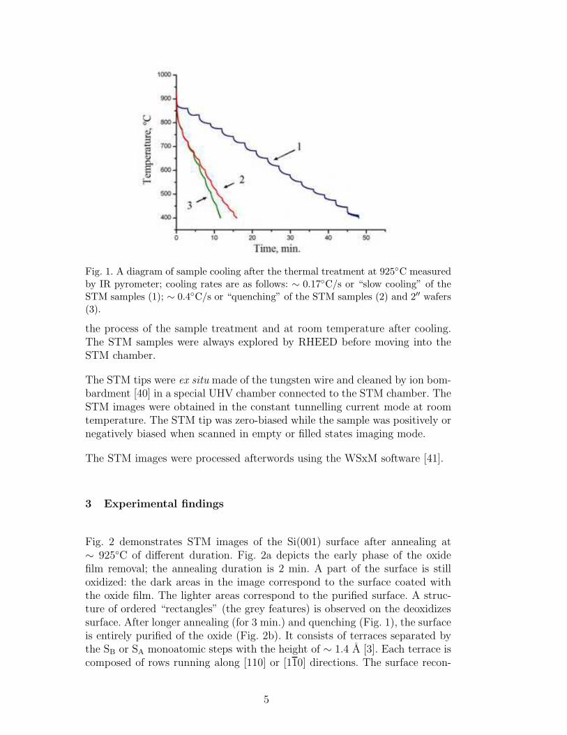
Fig. 1. A diagram of sample cooling after the thermal treatment at 925C measuredby IR pyrometer; cooling rates are as follows: ∼ 0.17C/s or “slow cooling” of theSTM samples (1); ∼ 0.4C/s or “quenching” of the STM samples (2) and 2′′ wafers(3).
the process of the sample treatment and at room temperature after cooling.The STM samples were always explored by RHEED before moving into theSTM chamber.
The STM tips were ex situ made of the tungsten wire and cleaned by ion bom-bardment [40] in a special UHV chamber connected to the STM chamber. TheSTM images were obtained in the constant tunnelling current mode at roomtemperature. The STM tip was zero-biased while the sample was positively ornegatively biased when scanned in empty or filled states imaging mode.
The STM images were processed afterwords using the WSxM software [41].
3 Experimental findings
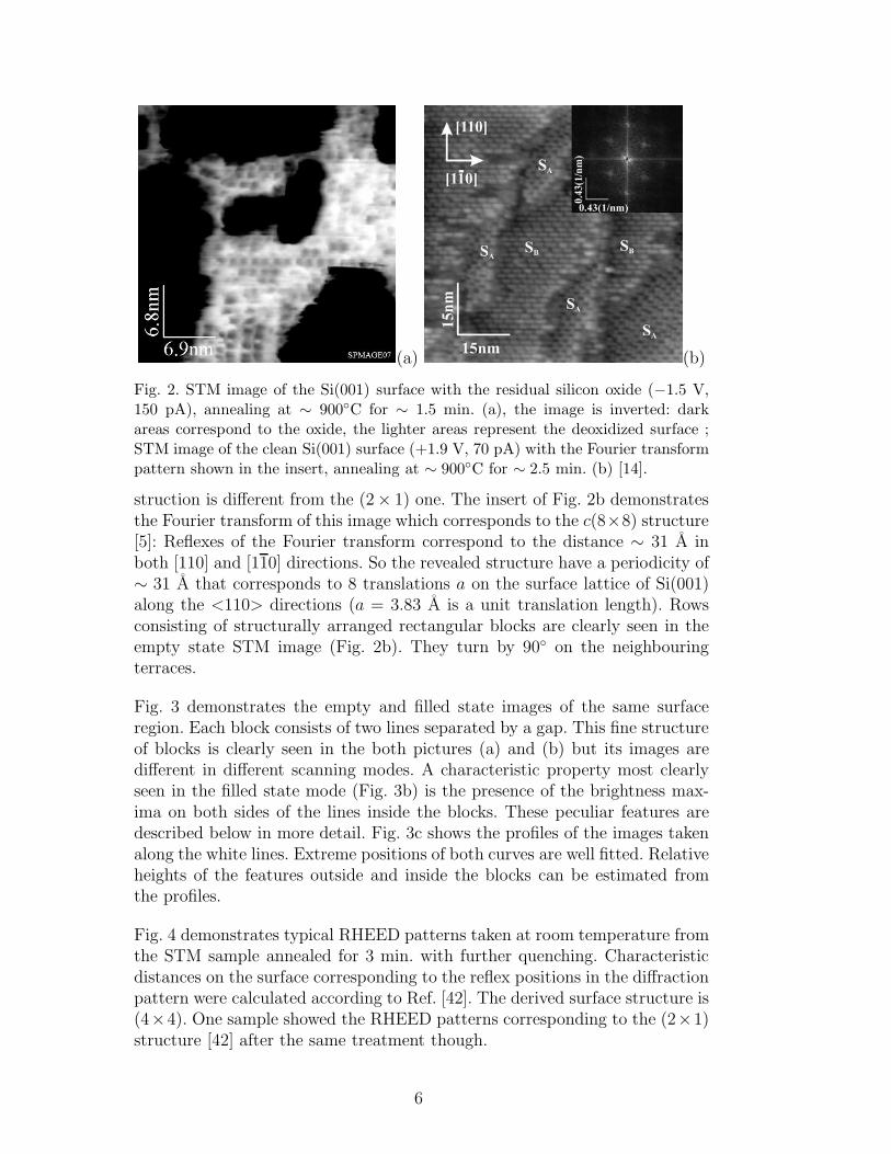
Fig. 2 demonstrates STM images of the Si(001) surface after annealing at∼ 925C of different duration. Fig. 2a depicts the early phase of the oxidefilm removal; the annealing duration is 2 min. A part of the surface is stilloxidized: the dark areas in the image correspond to the surface coated withthe oxide film. The lighter areas correspond to the purified surface. A struc-ture of ordered “rectangles” (the grey features) is observed on the deoxidizessurface. After longer annealing (for 3 min.) and quenching (Fig. 1), the surfaceis entirely purified of the oxide (Fig. 2b). It consists of terraces separated bythe SB or SA monoatomic steps with the height of ∼ 1.4 A [3]. Each terrace iscomposed of rows running along [110] or [110] directions. The surface recon-
5
(a) (b)
Fig. 2. STM image of the Si(001) surface with the residual silicon oxide (−1.5 V,150 pA), annealing at ∼ 900C for ∼ 1.5 min. (a), the image is inverted: darkareas correspond to the oxide, the lighter areas represent the deoxidized surface ;STM image of the clean Si(001) surface (+1.9 V, 70 pA) with the Fourier transformpattern shown in the insert, annealing at ∼ 900C for ∼ 2.5 min. (b) [14].
struction is different from the (2× 1) one. The insert of Fig. 2b demonstratesthe Fourier transform of this image which corresponds to the c(8×8) structure[5]: Reflexes of the Fourier transform correspond to the distance ∼ 31 A inboth [110] and [110] directions. So the revealed structure have a periodicity of∼ 31 A that corresponds to 8 translations a on the surface lattice of Si(001)along the <110> directions (a = 3.83 A is a unit translation length). Rowsconsisting of structurally arranged rectangular blocks are clearly seen in theempty state STM image (Fig. 2b). They turn by 90 on the neighbouringterraces.
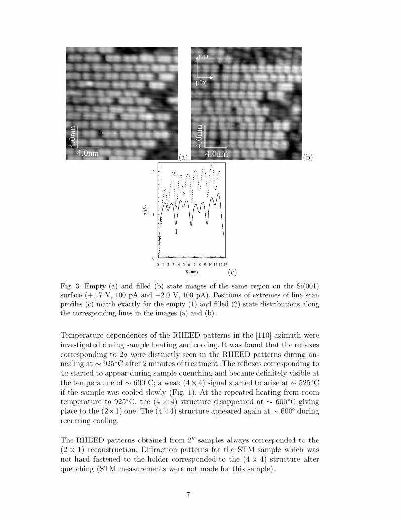
Fig. 3 demonstrates the empty and filled state images of the same surfaceregion. Each block consists of two lines separated by a gap. This fine structureof blocks is clearly seen in the both pictures (a) and (b) but its images aredifferent in different scanning modes. A characteristic property most clearlyseen in the filled state mode (Fig. 3b) is the presence of the brightness max-ima on both sides of the lines inside the blocks. These peculiar features aredescribed below in more detail. Fig. 3c shows the profiles of the images takenalong the white lines. Extreme positions of both curves are well fitted. Relativeheights of the features outside and inside the blocks can be estimated fromthe profiles.
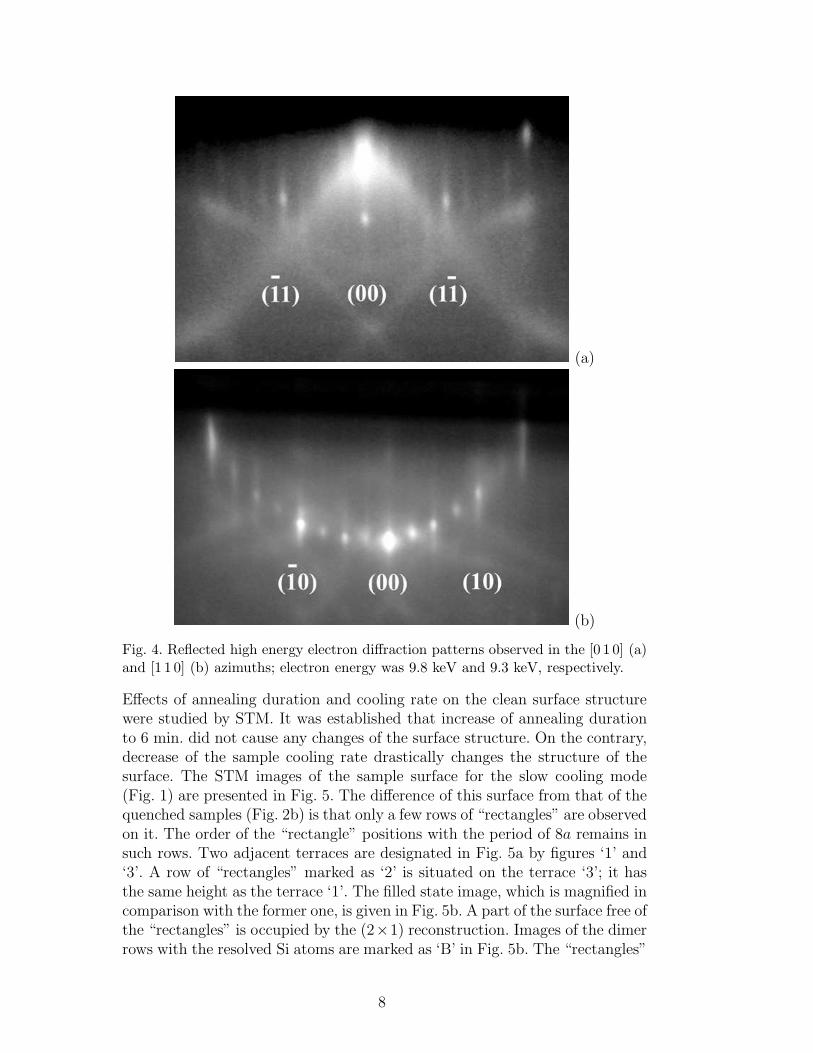
Fig. 4 demonstrates typical RHEED patterns taken at room temperature fromthe STM sample annealed for 3 min. with further quenching. Characteristicdistances on the surface corresponding to the reflex positions in the diffractionpattern were calculated according to Ref. [42]. The derived surface structure is(4×4). One sample showed the RHEED patterns corresponding to the (2×1)structure [42] after the same treatment though.
6
(a) (b)
(c)
Fig. 3. Empty (a) and filled (b) state images of the same region on the Si(001)surface (+1.7 V, 100 pA and −2.0 V, 100 pA). Positions of extremes of line scanprofiles (c) match exactly for the empty (1) and filled (2) state distributions alongthe corresponding lines in the images (a) and (b).
Temperature dependences of the RHEED patterns in the [110] azimuth wereinvestigated during sample heating and cooling. It was found that the reflexescorresponding to 2a were distinctly seen in the RHEED patterns during an-nealing at ∼ 925C after 2 minutes of treatment. The reflexes corresponding to4a started to appear during sample quenching and became definitely visible atthe temperature of ∼ 600C; a weak (4×4) signal started to arise at ∼ 525Cif the sample was cooled slowly (Fig. 1). At the repeated heating from roomtemperature to 925C, the (4 × 4) structure disappeared at ∼ 600C givingplace to the (2×1) one. The (4×4) structure appeared again at ∼ 600 duringrecurring cooling.
The RHEED patterns obtained from 2′′ samples always corresponded to the(2 × 1) reconstruction. Diffraction patterns for the STM sample which wasnot hard fastened to the holder corresponded to the (4 × 4) structure afterquenching (STM measurements were not made for this sample).
7
(a)
(b)
Fig. 4. Reflected high energy electron diffraction patterns observed in the [0 1 0] (a)and [1 1 0] (b) azimuths; electron energy was 9.8 keV and 9.3 keV, respectively.
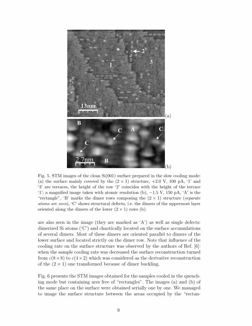
Effects of annealing duration and cooling rate on the clean surface structurewere studied by STM. It was established that increase of annealing durationto 6 min. did not cause any changes of the surface structure. On the contrary,decrease of the sample cooling rate drastically changes the structure of thesurface. The STM images of the sample surface for the slow cooling mode(Fig. 1) are presented in Fig. 5. The difference of this surface from that of thequenched samples (Fig. 2b) is that only a few rows of “rectangles” are observedon it. The order of the “rectangle” positions with the period of 8a remains insuch rows. Two adjacent terraces are designated in Fig. 5a by figures ‘1’ and‘3’. A row of “rectangles” marked as ‘2’ is situated on the terrace ‘3’; it hasthe same height as the terrace ‘1’. The filled state image, which is magnified incomparison with the former one, is given in Fig. 5b. A part of the surface free ofthe “rectangles” is occupied by the (2×1) reconstruction. Images of the dimerrows with the resolved Si atoms are marked as ‘B’ in Fig. 5b. The “rectangles”
8
(a)
(b)
Fig. 5. STM images of the clean Si(001) surface prepared in the slow cooling mode:(a) the surface mainly covered by the (2 × 1) structure, +2.0 V, 100 pA, ‘1’ and‘3’ are terraces, the height of the row ‘2’ coincides with the height of the terrace‘1’; a magnified image taken with atomic resolution (b), −1.5 V, 150 pA, ‘A’ is the“rectangle”, ‘B’ marks the dimer rows composing the (2 × 1) structure (separateatoms are seen), ‘C’ shows structural defects, i.e. the dimers of the uppermost layeroriented along the dimers of the lower (2× 1) rows (b).
are also seen in the image (they are marked as ‘A’) as well as single defects:dimerized Si atoms (‘C’) and chaotically located on the surface accumulationsof several dimers. Most of these dimers are oriented parallel to dimers of thelower surface and located strictly on the dimer row. Note that influence of thecooling rate on the surface structure was observed by the authors of Ref. [6]:when the sample cooling rate was decreased the surface reconstruction turnedfrom c(8×8) to c(4×2) which was considered as the derivative reconstructionof the (2× 1) one transformed because of dimer buckling.
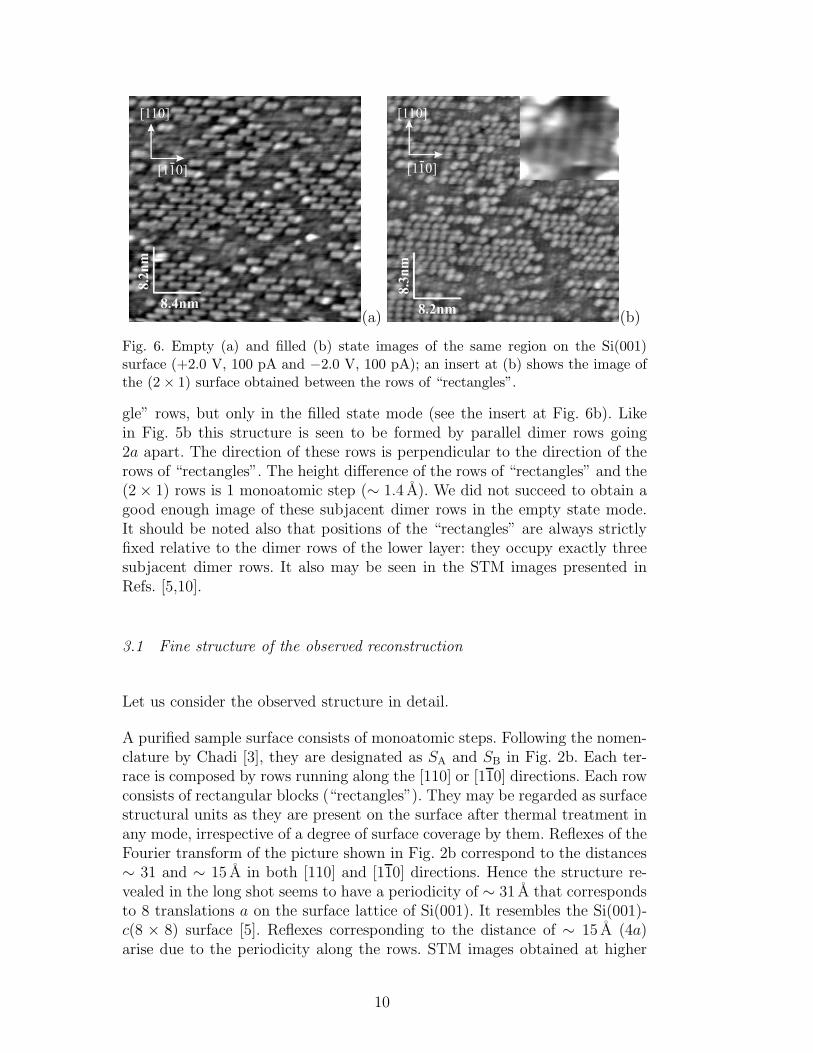
Fig. 6 presents the STM images obtained for the samples cooled in the quench-ing mode but containing ares free of “rectangles”. The images (a) and (b) ofthe same place on the surface were obtained serially one by one. We managedto image the surface structure between the areas occupied by the “rectan-
9
(a) (b)
Fig. 6. Empty (a) and filled (b) state images of the same region on the Si(001)surface (+2.0 V, 100 pA and −2.0 V, 100 pA); an insert at (b) shows the image ofthe (2× 1) surface obtained between the rows of “rectangles”.
gle” rows, but only in the filled state mode (see the insert at Fig. 6b). Likein Fig. 5b this structure is seen to be formed by parallel dimer rows going2a apart. The direction of these rows is perpendicular to the direction of therows of “rectangles”. The height difference of the rows of “rectangles” and the(2× 1) rows is 1 monoatomic step (∼ 1.4 A). We did not succeed to obtain agood enough image of these subjacent dimer rows in the empty state mode.It should be noted also that positions of the “rectangles” are always strictlyfixed relative to the dimer rows of the lower layer: they occupy exactly threesubjacent dimer rows. It also may be seen in the STM images presented inRefs. [5,10].
3.1 Fine structure of the observed reconstruction
Let us consider the observed structure in detail.
A purified sample surface consists of monoatomic steps. Following the nomen-clature by Chadi [3], they are designated as SA and SB in Fig. 2b. Each ter-race is composed by rows running along the [110] or [110] directions. Each rowconsists of rectangular blocks (“rectangles”). They may be regarded as surfacestructural units as they are present on the surface after thermal treatment inany mode, irrespective of a degree of surface coverage by them. Reflexes of theFourier transform of the picture shown in Fig. 2b correspond to the distances∼ 31 and ∼ 15 A in both [110] and [110] directions. Hence the structure re-vealed in the long shot seems to have a periodicity of ∼ 31 A that correspondsto 8 translations a on the surface lattice of Si(001). It resembles the Si(001)-c(8 × 8) surface [5]. Reflexes corresponding to the distance of ∼ 15 A (4a)arise due to the periodicity along the rows. STM images obtained at higher
10
(a) (b)
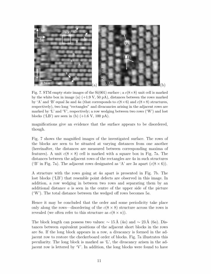
Fig. 7. STM empty state images of the Si(001) surface ; a c(8×8) unit cell is markedby the white box in image (a) (+1.9 V, 50 pA), distances between the rows markedby ‘A’ and ‘B’ equal 3a and 4a (that corresponds to c(8×6) and c(8×8) structures,respectively), two long “rectangles” and divacancies arising in the adjacent rows aremarked by ‘L’ and ‘V’, respectively; a row wedging between two rows (‘W’) and lostblocks (‘LB’) are seen in (b) (+1.6 V, 100 pA).
magnifications give an evidence that the surface appears to be disordered,though.
Fig. 7 shows the magnified images of the investigated surface. The rows ofthe blocks are seen to be situated at varying distances from one another(hereinafter, the distances are measured between corresponding maxima offeatures). A unit c(8 × 8) cell is marked with a square box in Fig. 7a. Thedistances between the adjacent rows of the rectangles are 4a in such structures(‘B’ in Fig. 7a). The adjacent rows designated as ‘A’ are 3a apart (c(8× 6)).
A structure with the rows going at 4a apart is presented in Fig. 7b. Thelost blocks (‘LB’) that resemble point defects are observed in this image. Inaddition, a row wedging in between two rows and separating them by anadditional distance a is seen in the centre of the upper side of the picture(‘W’). The total distance between the wedged off rows becomes 5a.
Hence it may be concluded that the order and some periodicity take placeonly along the rows—disordering of the c(8 × 8) structure across the rows isrevealed (we often refer to this structure as c(8× n)).
The block length can possess two values: ∼ 15 A (4a) and ∼ 23 A (6a). Dis-tances between equivalent positions of the adjacent short blocks in the rowsare 8a. If the long block appears in a row, a divacancy is formed in the ad-jacent row to restore the checkerboard order of blocks. Fig. 7a illustrates thispeculiarity. The long block is marked as ‘L’, the divacancy arisen in the ad-jacent row is lettered by ‘V’. In addition, the long blocks were found to have
11

(a) (b)
Fig. 8. Empty state (a) and filled state (b) images of the same region onSi(001)-c(8 × n) surface (+1.7 V, 150 pA, and −2.2 V, 120 pA). Correspondingschematic drawings of the surface structure are superimposed on both pictures.The lighter circles are the higher the corresponding atom is situated in the surfacestructure. The dimer buckling is observed in the filled state image, which is re-flected in the drawing by larger open circles representing higher atoms of the tiltedSi dimers of the uppermost layer of the structure.
one more peculiarity. They have extra maxima in their central regions. Themaxima are not so pronounced as the main ones but nevertheless they arequite recognizable in the pictures (Fig. 7a).
Fig. 8 presents magnified STM images of the blocks (“short rectangles”). Theimages obtained in the empty-state (Fig. 8a) and filled-state (Fig. 8b) modesare different. In the empty-state mode, short blocks look like two lines sepa-rated by ∼ 8 A (the distance is measured between brightness maxima in eachline). It is a maximum measured value which can lessen depending on scanningparameters. Along the rows, each block is formed by two parts. The distancebetween the brightness maxima of these parts is ∼ 11.5 A (or some greater de-pending on scanning parameters). In the filled-state mode, the block divisioninto two structurally identical parts remains. Depending on scanning condi-tions, each part looks like either bright coupled dashes and blobs (Figs. 3band 6b) or two links (brightness maxima) of zigzag chains (Fig. 8b). The dis-tances between the maxima are ∼ 4 A along the rows; this value grows withincreasing tunneling current.
The presented STM data are interpreted by us as a structure composed by Siad-dimers and divacancies.
12
(a) (b)
(c)
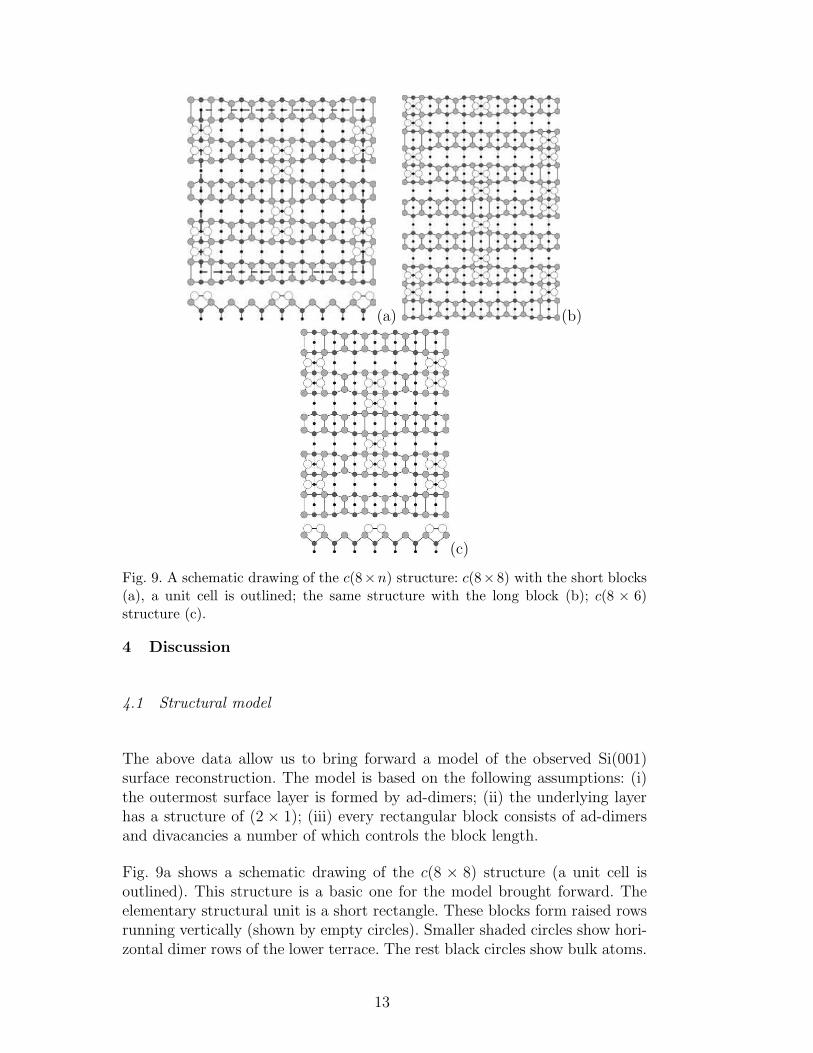
Fig. 9. A schematic drawing of the c(8×n) structure: c(8×8) with the short blocks(a), a unit cell is outlined; the same structure with the long block (b); c(8 × 6)structure (c).
4 Discussion
4.1 Structural model
The above data allow us to bring forward a model of the observed Si(001)surface reconstruction. The model is based on the following assumptions: (i)the outermost surface layer is formed by ad-dimers; (ii) the underlying layerhas a structure of (2 × 1); (iii) every rectangular block consists of ad-dimersand divacancies a number of which controls the block length.
Fig. 9a shows a schematic drawing of the c(8 × 8) structure (a unit cell isoutlined). This structure is a basic one for the model brought forward. Theelementary structural unit is a short rectangle. These blocks form raised rowsrunning vertically (shown by empty circles). Smaller shaded circles show hori-zontal dimer rows of the lower terrace. The rest black circles show bulk atoms.
13
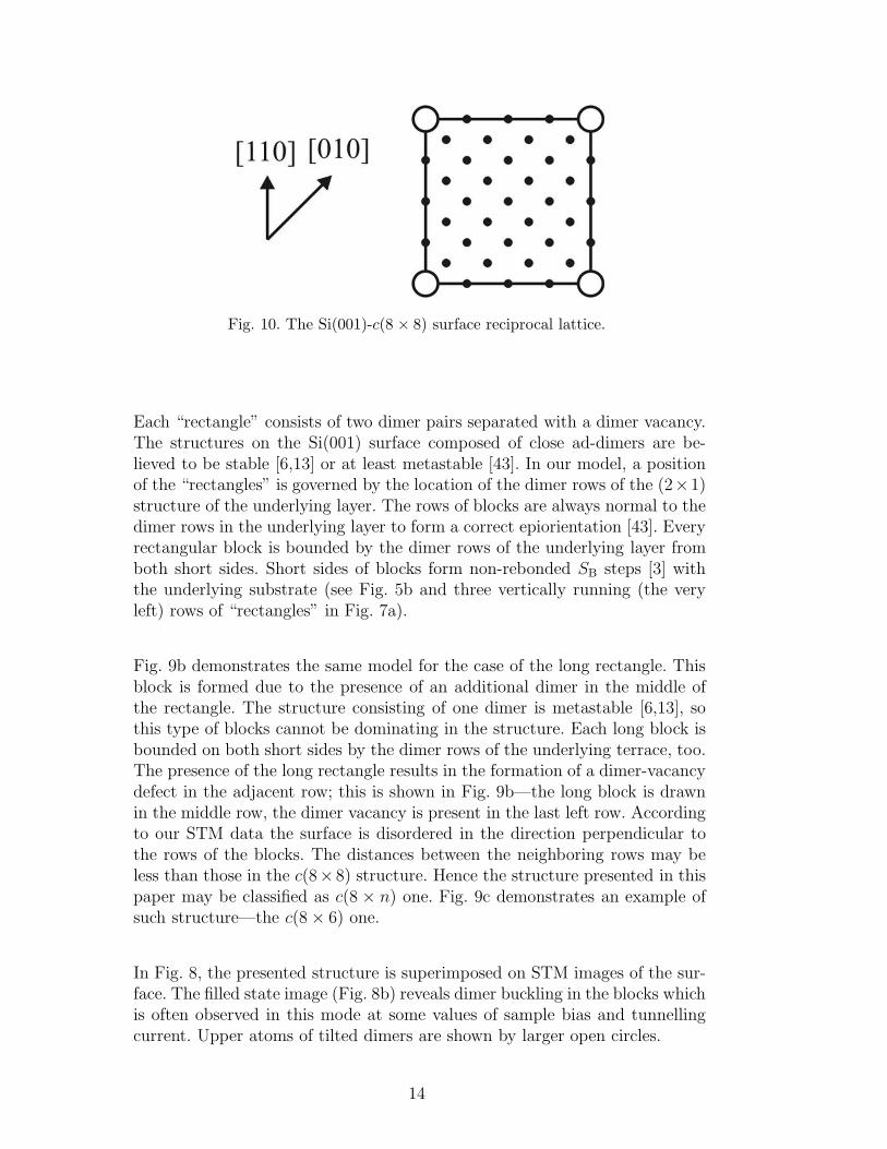
Fig. 10. The Si(001)-c(8 × 8) surface reciprocal lattice.
Each “rectangle” consists of two dimer pairs separated with a dimer vacancy.The structures on the Si(001) surface composed of close ad-dimers are be-lieved to be stable [6,13] or at least metastable [43]. In our model, a positionof the “rectangles” is governed by the location of the dimer rows of the (2×1)structure of the underlying layer. The rows of blocks are always normal to thedimer rows in the underlying layer to form a correct epiorientation [43]. Everyrectangular block is bounded by the dimer rows of the underlying layer fromboth short sides. Short sides of blocks form non-rebonded SB steps [3] withthe underlying substrate (see Fig. 5b and three vertically running (the veryleft) rows of “rectangles” in Fig. 7a).
Fig. 9b demonstrates the same model for the case of the long rectangle. Thisblock is formed due to the presence of an additional dimer in the middle ofthe rectangle. The structure consisting of one dimer is metastable [6,13], sothis type of blocks cannot be dominating in the structure. Each long block isbounded on both short sides by the dimer rows of the underlying terrace, too.The presence of the long rectangle results in the formation of a dimer-vacancydefect in the adjacent row; this is shown in Fig. 9b—the long block is drawnin the middle row, the dimer vacancy is present in the last left row. Accordingto our STM data the surface is disordered in the direction perpendicular tothe rows of the blocks. The distances between the neighboring rows may beless than those in the c(8×8) structure. Hence the structure presented in thispaper may be classified as c(8 × n) one. Fig. 9c demonstrates an example ofsuch structure—the c(8× 6) one.
In Fig. 8, the presented structure is superimposed on STM images of the sur-face. The filled state image (Fig. 8b) reveals dimer buckling in the blocks whichis often observed in this mode at some values of sample bias and tunnellingcurrent. Upper atoms of tilted dimers are shown by larger open circles.
14
(a) (b)
(c)
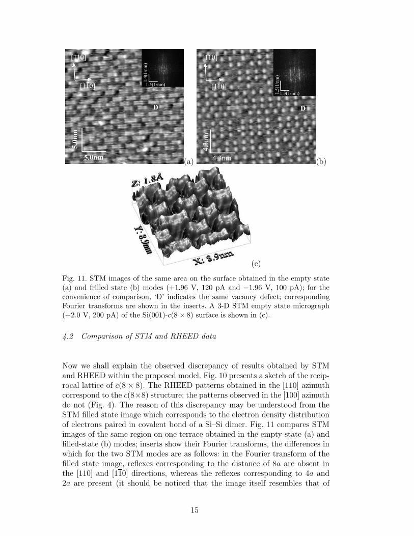
Fig. 11. STM images of the same area on the surface obtained in the empty state(a) and frilled state (b) modes (+1.96 V, 120 pA and −1.96 V, 100 pA); for theconvenience of comparison, ‘D’ indicates the same vacancy defect; correspondingFourier transforms are shown in the inserts. A 3-D STM empty state micrograph(+2.0 V, 200 pA) of the Si(001)-c(8 × 8) surface is shown in (c).
4.2 Comparison of STM and RHEED data
Now we shall explain the observed discrepancy of results obtained by STMand RHEED within the proposed model. Fig. 10 presents a sketch of the recip-rocal lattice of c(8× 8). The RHEED patterns obtained in the [110] azimuthcorrespond to the c(8×8) structure; the patterns observed in the [100] azimuthdo not (Fig. 4). The reason of this discrepancy may be understood from theSTM filled state image which corresponds to the electron density distributionof electrons paired in covalent bond of a Si–Si dimer. Fig. 11 compares STMimages of the same region on one terrace obtained in the empty-state (a) andfilled-state (b) modes; inserts show their Fourier transforms, the differences inwhich for the two STM modes are as follows: in the Fourier transform of thefilled state image, reflexes corresponding to the distance of 8a are absent inthe [110] and [110] directions, whereas the reflexes corresponding to 4a and2a are present (it should be noticed that the image itself resembles that of
15
the (4 × 4) reconstructed surface). If an empty state image is not available,it might be concluded that the (4 × 4) structure is arranged on the surface.An explanation of this observation is simple. Main contribution to the STMimage is made by ad-dimers situated on the sides of the “rectangles”, i. e. ontops of the underlying dimer rows. According to calculations made, e. g., inRefs. [44,45] dimers located in such a way are closer to the STM tip and lookin the images brighter than those situated in the troughs. Hence, it may beconcluded that the RHEED (4×4) pattern results from electron diffraction onthe extreme dimers of the “rectangles” forming the c(8× 8) surface structure.
The latter statement is illustrated by the STM 3-D empty-state topographshown in Fig. 11c. The extreme dimers located on the sides of the rectangularblocks are seen to be somewhat higher than the other ones of the dimer pairs;they form a superfine relief which turned out to be sufficient to backscatterfast electrons incident on the surface at grazing angles.
4.3 Origin
The Si(001)-c(8×8) structure have formerly been observed and described in anumber of publications [4,5,6,7,10]. Conditions of its formation were different:coper atoms were deposited on silicon (2 × 1) surface to form the c(8 × 8)reconstruction [10], although it is known that Cu atoms are not absorbed onthe Si(001) clean surface if the sample temperature is greater than 600C,and on the contrary Cu desorption from the surface takes place [7,10]; fastcooling from the annealing temperature of∼ 1100C was applied [4,5]; samplestreated in advance by ion bombardment were annealed and rapidly cooled [6].The resultant surfaces were mainly explored by STM and low energy electrondiffraction (LEED). STM investigations yielded alike results—a basic unitof the reconstruction was a “rectangle”, but the structure of the “rectangles”revealed by different authors was different. In general, an origin of the Si(001)-c(8× 8) structure is unclear now.
STM images most resembling our data were reported in Ref. [5]. In that paper,the c(8 × 8) structure was observed in samples without special treatmentby coper: the samples were subjected to annealing at the temperature of ∼1050C for the oxide film removal. Formation of the c(8×8) reconstruction wasexplained in that article by the presence of a trace amount of Cu atoms theconcentration of which was beyond the Auger electron spectroscopy detectionthreshold. The STM empty state images of the samples were similar to thosepresented in the current paper. A very important difference is observed in thefilled state images—we observe absolutely different configuration of dimerswithin the “rectangles”. Nevertheless, the presence of Cu cannot be completelyexcluded. Some amount of the Cu atoms may come on the surface from the
16

construction materials of the MBE chamber (although there is a circumstancethat to some extent contradicts this viewpoint: Cu atoms were not detectedin the residual atmosphere of the MBE chamber within the sensitivity limit ofthe SRS RGA-200 mass spectrometer) or even from the Si wafer. Cu is knownto be a poorly controllable impurity and its concentration in the subsurfacelayers of Si wafers which were not subjected to the gettering process mayreach 1015 cm−3. This amount of Cu may appear to be sufficient to give riseto the formation of the defect surface reconstruction. However, the followingarguments urge us to doubt about the Cu-based model: (i) undetectable traceamounts of Cu were suggested in Ref. [5], the presence or absence of whichis unprovable; (ii) even if the suggestion is true, our STM images give anevidence of a different amount of dimers in the rectangular blocks, so, it isunclear why Cu atoms form different stable configurations on similar surfaces;and (iii) it is hard to explain why Cu atoms cyclically compose and decomposethe rectangular blocks during the cyclical thermal treatments of the samples.It applies equally to any other impurity or contamination.
Now we consider a different interpretation of our data. As mentioned above,literature suggests two causes of c(8 × 8) appearance. The first is an impactof impurity atoms adsorbed on the surface even at trace concentrations. Thesecond is a thermal cycle of the oxide film decomposition and sample cooling.The first model seems to be hardly applicable for explanation of the reportedexperimental results. According to our data, there are no impurities adsorbeddirectly on the studied surface: RHEED patterns correspond to a clean Si(001)surface reconstructed in (2×1) or, at lower temperatures, (4×4) configuration.Cyclic contaminant desorption at high temperatures (& 600C) and adsorp-tion on sample cooling is unbelievable. Consecutive segregation and desegre-gation of an undetectable impurity in subsurface layers also does not seemverisimilar.
The second explanation looks more attractive. It was found in Ref. [46] as aresult of the STM studies that the Si(001) surface subjected to the thermaltreatment at ∼ 820C which was used for decomposition of the thin (∼ 1 nmthick) SiO2 films obtained by chemical oxidation contained a high density ofvacancy-type defects and their agglomerates as well as individual ad-dimers.So, the initial bricks for the considered surface structure are abundant afterthe SiO2 decay.
Literature presents a wide experimental material on a different reconstruc-tion of the Si(001) surface—c(4× 4)—which also arise at the temperatures of& 600C. For example, a review of articles describing different experimentalinvestigations can be found in Refs. [12,31,32,33,34,35]. Based on the general-ized data, an inference can be made that the c(4 × 4) structure forms in theinterval from 600 to 700C. Most likely, at these temperatures an appreciablemigration of Si ad-atoms starts on surface. The structure is free of impuri-
17
(a) (b)
(c)
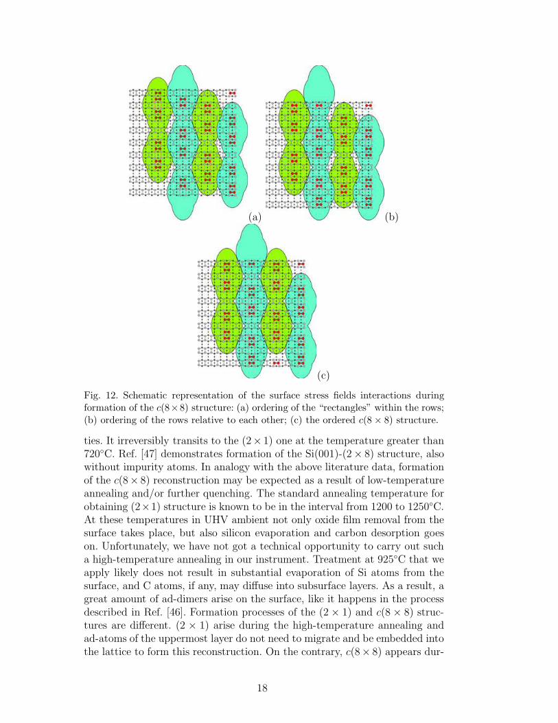
Fig. 12. Schematic representation of the surface stress fields interactions duringformation of the c(8×8) structure: (a) ordering of the “rectangles” within the rows;(b) ordering of the rows relative to each other; (c) the ordered c(8× 8) structure.
ties. It irreversibly transits to the (2× 1) one at the temperature greater than720C. Ref. [47] demonstrates formation of the Si(001)-(2× 8) structure, alsowithout impurity atoms. In analogy with the above literature data, formationof the c(8× 8) reconstruction may be expected as a result of low-temperatureannealing and/or further quenching. The standard annealing temperature forobtaining (2×1) structure is known to be in the interval from 1200 to 1250C.At these temperatures in UHV ambient not only oxide film removal from thesurface takes place, but also silicon evaporation and carbon desorption goeson. Unfortunately, we have not got a technical opportunity to carry out sucha high-temperature annealing in our instrument. Treatment at 925C that weapply likely does not result in substantial evaporation of Si atoms from thesurface, and C atoms, if any, may diffuse into subsurface layers. As a result, agreat amount of ad-dimers arise on the surface, like it happens in the processdescribed in Ref. [46]. Formation processes of the (2 × 1) and c(8 × 8) struc-tures are different. (2 × 1) arise during the high-temperature annealing andad-atoms of the uppermost layer do not need to migrate and be embedded intothe lattice to form this reconstruction. On the contrary, c(8× 8) appears dur-
18
ing sample cooling, at rather low temperatures, and at the moment of a priorannealing the uppermost layer consists of abundant ad-atoms. On cooling thead-dimers have to migrate along the surface and be build in the lattice. A num-ber of competing sinks may exist on the surface (steps, vacancies, etc.), buthigh cooling rate may impede ad-atom annihilation slowing their migrationto sinks and in such way creating supersaturation and favoring 2-D islanding,and freezing a high-order reconstruction.
The following scenario may be proposed to describe the c(8 × 8) structureformation. A large number of ad-dimers remains on the surface during thesample annealing after the oxide film removal. They form the uppermost layerof the structure. The underlying layer is (2× 1) reconstructed. Ad-dimers aremobile and can form different complexes (islands). Calculations show that themost energetically favorable island configurations are single dimer on a rowin non-epitaxial orientation [43,45,48,49] (Fig. 5b), complexes of two dimers(pairs of dimers) in epi-orientation (metastable [43]) and two dimers on a rowin non-epitaxial orientation separated by a divacancy, and tripple-dimer epi-islands considered as critical epinuclei [43]. These mobile dimers and complexesmigrate in the stress field of the (2× 1) structure. The sinks for ad-dimers are(A) steps, (B) vacancy defects of the underlying (2 × 1) reconstructed layer,and (C) “fastening” them to the (2×1) surface as a c(8×8) structure. The mainsinks at high temperatures are A and B. As the sample is cooled, the C sinkbecomes dominating. Ad-dimers on the Si(001)-(2 × 1) surface are known totend to form dimer rows [50]. In this case such rows are formed by metastabledimer pairs gathered in the “rectangles”. The “rectangles” are ordered witha period of 8 translations in the rows. The ordering is likely controlled by the(2 × 1) structure of the underlying layer and interaction of the stress fieldsarising around each “rectangle”. Effect of the underlying (2× 1) layer is thatthe “rectangle” position on the surface relative to its dimer rows is strictlydefined: dimers of the “rectangle” edges must be placed on tops of the rows.Interaction of the stress fields initially arranges the “rectangles” within therows (Fig. 12a), then it arranges adjacent rows with respect to one another(Fig. 12b). The resultant ordered structure is shown in Fig. 12c. The describedbehaviour of “rectangles” can be derived from the STM images presented inthe previous sections. In addition, investigation of appearance of the RHEEDpatterns allowed us to conclude that the process of dimer ordering in thec(8×8) structure is gradual: the pattern reflexes appearing on transition from(2 × 1) to (4 × 4) reach maximum brightness gradually; it means that thec(8× 8) structure does not arise instantly throughout the sample surface, butoriginally form some nuclei (“standalone rectangles” like those in Fig. 5a) onwhich mobile ad-dimers crystallize in the ordered surface configuration.
19

4.4 Stability
A source of stability of the Si(001) surface configuration composed by ad-dimers gathered in the rectangular islands has not been found to date. Someof possible sources of stabilization of structures with high-order periodicitywere considered in Refs. [31,47,51,52,53]. One of likely reasons of high-orderstructure formation might be a non-uniformity of the stress field distributionon a sample surface and dependance of this distribution on such factors asprocess temperature, sample cooling rate, specimen geometry and a way ofsample fastening to a holder, presence of impurity atoms on and under thesurface. In this wise, it is clear only that ad-dimers form “rectangles” whichare energetically favorable at temperature conditions of the experiments.
In this connection, a guide for further consideration could be found in Ref. [43]where an issue of the critical epinucleus—or the smallest island which unre-constructs the surface and whose probability of growth is greater than likeli-hood of decay—on the (2× 1) reconstructed Si(001) was theoretically investi-gated. First-principle calculations showed that dimer pairs in epi-orientationare metastable and the epinucleus consists of tripple dimers [43]. Unfortu-nately, we failed to observe tripple-dimer islands in our experiments, and cal-culations were limited to three dimers in the cited article. Some formationssmaller than “rectangles” sometimes are observed in images of the rarifiedstructures (Fig. 5a) but they are likely single dimers (Fig. 5b) and dimer pairs.We believe that the short “rectangles” we deal with in this article might beconsidered as epinuclei for the c(8×n) structure because, although they showno tendency to grow themselves, they are both seeds and structural units forformation of larger islands such as chains (Fig. 5a), grouped chains (Fig. 2a)and complete ares (Fig. 6). From other hand, they also do not tend to decayor annihilate even on as powerful sinks as steps (Fig. 5a). Thus, we con-clude that the stability of such epi-islands as dimer pair-vacancy-pair (short“rectangles”, Fig. 9a,c) is the highest. Less probable (stable) configurationis pair-vacancy-dimer-vacancy-pair (long “rectangle”, Fig. 9b). We think itsless stability is due to presence of a single epi-oriented dimer in the centre.That is why long “rectangles” are much less spread on the Si(001) surfacethan the short ones and entire structure stabilization in the presence of thelong “rectangles” requires appearance of additional dimer vacancies between“rectangles” in adjacent rows in the vicinity of the long blocks.
5 Conclusion
In summary, it may be concluded that the Si(001) surface prepared under theconditions of the UHV MBE chamber in a standard wafer preparation cycle
20
has (8× n) reconstruction which is partly ordered only in one direction. Twotypes of unit blocks form the rows running along [110] and [110] axes. Whenthe long block disturbs the order in a row a dimer-vacancy defect appears inthe adjacent row in the vicinity of the long block to restore the checker-boardorder of blocks in the neighboring rows.
Discrepancy of RHEED patterns and STM images was detected. According toRHEED data, (2×1) and (4×4) structures can form the Si(001) surface duringsample treatment. STM studies of the same samples at room temperatureshow that a high-order c(8 × 8) reconstruction exists on the Si(001) surface;simultaneously, the underlying layer is (2× 1) reconstructed in the areas freeof the c(8×8) structure. A fraction of the surface area covered by the c(8×8)structure decreases as the sample cooling rate is reduced. RHEED patternscorresponding to the (4 × 4) reconstruction arise at ∼ 600C in the processof sample cooling after annealing. The reconstruction is reversible: the (4× 4)structure turns into the (2× 1) one at ∼ 600C in the process of the repeatedsample heating, the (4×4) structure appears on the surface again at the sametemperature during recurring cooling.
A model of the c(8 × 8) structure based on epi-oriented ad-dimer complexeshas been presented. Ordering of the ad-dimer complexes likely arise due tointeraction of the stress fiends produced by them. The discrepancy of theSTM and RHEED data has been explained within the proposed model: thec(8 × 8) structure revealed by STM has been evidenced to manifest itself asthe (4× 4) one in the RHEED patterns.
Probable causes of the c(8 × 8) reconstructed Si(001) surface formation havebeen discussed. A combination of low temperature of sample annealing andhigh rate of its cooling may be considered as one of the most plausible factorsresponsible for its appearance. The structural units of the studied reconstruc-tion are supposed to be its critical epinuclei.
6 Acknowledgements
The research was supported by the Science and Innovations Agency of RFunder the State Contract No. 02.513.11.3130 and the Education Agency ofRF under the State Contract No. Π2367.
21
References
[1] V. A. Yuryev, L. V. Arapkina, V. A. Chapnin, V. P. Kalinushkin, N. V.Kiryanova, O. V. Uvarov, K. V. Chizh, L. A. Krylova, R. O. Stepanov, O. O.Zaytsev, Development of physical and technological basis of the controllableformation of densely packed Ge nanocluster arrays on the silicon (100) surfaceby means of ultrahigh vacuum molecular beam epitaxy, Report on ResearchProject 2007-3-1.3-25-01-303 of the Science and Innovations Agency of theRussian Federation, A. M. Prokhorov General Physics Institute of the RussianAcademy of Sciences, Moscow, Russia, VNITC State Reg. No. 0220.0 802501(2007).
[2] R. J. Hamers, R. M. Tromp, J. E. Demuth, Scanning tunneling microscopy ofSi(001), Phys. Rev. B 34 (1986) 5343.
[3] D. J. Chadi, Stabilities of single-layer and bilayer steps on Si(001) surfaces,Phys. Rev. Lett. 59 (1987) 1691.
[4] X. Hu, Z. Lin, Hydrogen adsorption induced phase transitions on Si(100)-c(8×8): temperature dependence studied by LEED, Appl. Surf. Sci. 90 (1995) 111.
[5] P. W. Murray, R. Lindsay, F. M. Leibsle, P. L. Wincott, G. Thornton, Directobservation of the c(8×8) defect structure on Si(001) using scanning tunnellingmicroscopy, Phys. Rev. B 54 (1996) 13468.
[6] T. Kubo, T. Agura, N. Takagi, M. Nishijima, Investigation on the surfaceelectronic states of the Si(001) c(4×2) and c(8×8) surfaces: An electron energyloss spectroscopy study, Jpn. J. Appl. Phys. 36 (1997) L975.
[7] H. Iton, T. Ann, T. Kawasaki, T. Ichinokawa, Surface structures and growthmode of Cu/Si(100) surfaces by scanning tunnelling microscopy, Surf. Rev. Lett.5 (1998) 747.
[8] J.-Y. Koo, J.-Y. Yi, C. Hwang, D.-H. Kim, G. Lee, S. Lee, Basic structure ofthe kinked monatomic steps on the Si(001) surface, Phys. Rev. B 57 (1998)8782.
[9] K. Hata, S. Yasuda, H. Shigekawa, Reinterpretation of the scanning tunnellingmicroscopy images of Si(100)-(2 × 1) dimers, Phys. Rev. B 60 (1999) 8164.
[10] B. Z. Liu, M. V. Katkov, J. Nogami, An STM study of Cu on Si(001) in thec(8 × 8) structure, Surf. Sci. 453 (2000) 137.
[11] H. Okada, Y. Fujimoto, K. Endo, K. Hirose, Y. Mori, Detailed analysis ofscanning tunneling microscopy images of the Si(001) reconstructed surface withbuckled dimers, Phys. Rev. B 63 (2001) 195324.
[12] A. Goryachko, P. V. Melnik, N. G. Nakhodkin, T. V. Afanasjeva, I. F.Koval, New features of the Si(100)-c(4× 4) reconstruction observed with STM:suggestion of the structure with lowered symmetry, Surf. Sci. 497 (2002) 47.
22

[13] H. W. Liu, H. Q. Yang, H. M. Guo, Y. L. Wang, X. Lin, S. J. Pang, H. J.Gao, Patterns formed on the dimer vacancy array of Si(100) by self-assembly,Nanotechnol. 13 (2002) 729.
[14] L. V. Arapkina, V. M. Shevlyuga, V. A. Yuryev, Structure and peculiaritiesof the (8 × n)-type Si(001) surface prepared in a molecular beam epitaxychamber: A scanning tunneling microscopy study, JETP Lett. 87 (2008) 215,arXiv:0908.1346.
[15] L. V. Arapkina, K. V. Chizh, V. M. Shevlyuga, V. A. Yuryev, The controllableformation of densely packed arrays of Ge nanoclusters on the silicon (001)surface by means of ultrahigh vacuum molecular beam epitaxy, in: A. L.Aseev, A. V. Dvurechenskii (Eds.), Russian Conference on Actual Problems ofSemiconductor Photoelectronics (“Photonics-2008”), A. V. Rzhanov Institute ofSemiconductor Physics of Siberian Brunch of the Russian Academy of Sciences,Novosibirsk, Russia, 2008, p. 48.
[16] L. V. Arapkina, V. A. Yuryev, V. M. Shevlyuga, STM and RHEEDinvestigations of the c(8×n) defect structure on Si(001), in: 25-th InternationalConference on Defects in Semiconductors (ICDS-25), St. Petersburg, Russia,2009, p. 348.
[17] L. V. Arapkina, V. A. Yuryev, K. V. Chizh, V. A. Chapnin, Nucleation andgrowth of Ge hut clusters on the Si(001) surface at low temperatures, in: Proc.XIV Int. Symp. “Nanophysics and nanoelectronics”, Vol. 2, Inst. Microstruct.Phys. RAS, Nizhni Novgorod, Russia, 2010, p. 531.
[18] A. V. Dvurechenskii, V. A. Zinoviev, V. A. Kudryavtsev, J. V. Smagina, Effectsof low-energy ion irradiation on Ge/Si heteroepitaxy from molecular beam,JETP Lett. 72 (3) (2000) 131.
[19] A. V. Dvurechenskii, V. A. Zinoviev, J. V. Smagina, Self-organization of anensemble of Ge nanoclusters upon pulsed irradiation with low-energy ionsduring heteroepitaxy on Si, JETP Lett. 74 (2001) 267.
[20] A. V. Dvurechenskii, V. A. Zinovyev, V. A. Kudryavtsev, J. V. Smagina, P. L.Novikov, S. A. Teys, Ion-beam assisted surface islanding during Ge MBE on Si,Phys. Low-Dim. Struct. 1/2 (2002) 303.
[21] A. V. Dvurechenskii, J. V. Smagina, V. A. Zinoviev, V. A. Armbrister, V. A.Volodin, M. D. Efremov, Elemental composition of nanoclusters formed bypulsed irradiation with low-energy ions during Ge/Si epitaxy, JETP Lett. 79 (7)(2004) 333.
[22] A. V. Dvurechenskii, J. V. Smagina, V. A. Zinovyev, S. A. Teys, A. K.Gutakovskii, Modification of growth mode of Ge on Si by pulsed low-energyion-beam irradiation, Int. J. Nanoscience 3 (1/2) (2004) 19.
[23] A. V. Dvurechenskii, J. V. Smagina, R. Groetzschel, V. A. Zinoviev, V. A.Armbrister, P. L. Novikov, S. A. Teys, A. K. Gutakovskii, Ge/Si quantum dotnanostructures grown with low-energy ion beam-epitaxy, Surf. Coat. Technol.196 (1–3) (2005) 25.
23
[24] A. V. Dvurechenskii, J. V. Smagina, V. A. Armbrister, V. A. Zinovyev,P. L. Novikov, S. A. Teys, R. Groetzschel, Ge/Si nanostructures withquantum dots grown by ion-beam-assisted heteroepitaxy, in: B. Joyce,P. Kelires, A. Naumovets, D. Vvedensky (Eds.), Quantum Dots: Fundamentals,Applications and Frontiers, Kluwer Academic Publishers, Netherlands, 2005, p.135.
[25] N. P. Stepina, A. V. Dvurechenskii, V. A. Armbrister, J. V. Smagina, V. A.Volodin, A. V. Nenashev, J. P. Leitao, M. C. do Carmo, N. A. Sobolev, MBEgrowth of Ge/Si quantum dots upon low-energy pulsed ion irradiation, ThinSolid Films 517 (2008) 309.
[26] J. V. Smagina, V. A. Zinovyev, A. V. Nenashev, A. V. Dvurechenskii, V. A.Armbrister, S. A. Teys, Self-assembly of germanium islands under pulsedirradiation by a low-energy ion beam during heteroepitaxy of Ge/Si(100)structures, JETP 106 (2008) 517.
[27] L. V. Arapkina, V. A. Yuryev, Classification of Ge hut clusters in arrays formedby molecular beam epitaxy at low temperatures on the Si(001) surface, Phys.-Usp. 53 (3) (2010) 279, arXiv:0907.4770.
[28] L. V. Arapkina, V. A. Yuryev, Atomic structure of Ge quantum dots on theSi(001) surface, JETP Lett. 91 (6) (2010) 281, arXiv:0908.0883.
[29] L. V. Arapkina, V. A. Yuryev, Nucleation of Ge quantum dots on the Si(001)surface, Phys. Rev. B 82 (2010), to be published, arXiv:0907.4665.
[30] V. A. Yuryev, L. V. Arapkina, Defects of Ge quantum dot arrays on the Si(001)surface, Physica B 404 (2009) 4719, arXiv:0908.0841.
[31] K. Miki, K. Sakamoto, T. Sakamoto, Is the c(4 × 4) reconstruction of Si(001)associated with the presence of carbon?, Appl. Phys. Lett. 71 (1997) 3266.
[32] R. I. G. Uhrberg, J. E. Northrup, D. K. Biegelsen, R. D. Bringans, L.-E. Swartz,Atomic structure of the metastable c(4×4) reconstruction of Si(100), Phys. Rev.B 46 (1992) 10251.
[33] Z. Zhang, M. A. Kulakov, B. Bullemer, Scanning tunnelling microscopy studyof Si(100)-c(4x4) structure formation by annealing of Si epitaxial films, Surf.Sci. 69 (1996) 369.
[34] Z. Zhang, M. A. Kulakov, B. Bullemer, Surface morphology and reconstructionsof ultra thin Si films growth by solid-phase epitaxy, Thin Solid Films 294 (1997)88.
[35] F. K. Men, J. L. Erskine, Metastable oxygen-induced ordered structure on theSi(001) surface, Phys. Rev. B 50 (1994) 11200.
[36] K. N. Eltsov, Ultrahigh vacuum scanning tunnelling microscope STM GPI-300,http://surface.gpi.ru/papers/gpi300e.pdf.
24
[37] K. N. Eltsov, A. N. Klimov, A. N. Kosyakov, O. V. Obyedkov, V. M. Shevlyuga,V. Y. Yurov, Ultrahigh vacuum scanning funnelling microscope GPI-300, in:V. I. Konov, K. N. Eltsov (Eds.), Chemical state and atomic structure of fccmetal surfaces in chemical reaction with halogens, Vol. 59 of Proc. GeneralPhys. Inst., Nauka, Moscow, Russia, 2003, p. 45.
[38] V. Y. Yurov, A. N. Klimov, Scanning tunneling microscope calibration andreconstruction of real image—drift and slope elimination, Rev. Sci. Instrum. 65(1994) 1551.
[39] I. V. Kiryushina, Processes of liquid chemical preparation of silicon wafers in theVLSI production with sub-micrometer design rules, Ph.D. thesis, JSC Mikron,Zelenograd, Moscow, Russia, in Russian (2003).
[40] K. N. Eltsov, V. M. Shevlyuga, V. Y. Yurov, A. V. Kvit, M. S. Kogan, Sharptungsten tips prepared for STM study of deep nanostructures in UHV, Phys.Low-Dim. Struct. 9/10 (1996) 7.
[41] I. Horcas, R. Fernandez, J. M. Gomez-Rodriguez, J. Colchero, J. Gomez-Herrero, A. M. Baro, WSxM: A software for scanning probe microscopy anda tool for nanotechnology, Rev. Sci. Instrum. 78 (2007) 013705.
[42] J. E. Mahan, K. M. Geib, G. Y. Robinson, R. G. Long, A review of thegeometrical fundamentals of reflection high-energy electron diffraction withapplication to silicon surfaces, J. Vac. Sci. Technol. A 8 (1990) 3692.
[43] R. G. S. Pala, F. Liu, Critical epinucleation on reconstructed surfaces and first-principle calculation of homonucleation on Si(001), Phys. Rev. Lett. 95 (2005)136106.
[44] Z. Zhang, F. Wu, H. J. Zandvliet, B. Poelsema, H. Metiu, M. G. Lagally,Energetics and dynamics of Si ad-dimers on Si(001), Phys. Rev. Lett. 74 (1995)3644.
[45] G. Brocks, P. J. Kelly, R. Car, The energetics of adatoms on the Si(100) surface,Surf. Sci. 269/270 (1992) 860.
[46] A. Ney, J. J. Schulz, C. Pampuch, L. Peripelittchenko, R. Koch, Atomicstructure of low temperature prepared Si(001) substrates, Surf. Sci. 520 (2002)L633.
[47] T. Aruga, Y. Murata, Ordered-defect model for Si(001)−(2× 8), Phys. Rev. B34 (1986) 5654.
[48] Z. Zhang, H. Metiu, The self-organization of Si atoms adsorbed on a Si(100)surface: an atomic level kinetic model, Surf. Sci. Lett. 292 (1993) L781.
[49] K. Terakura, T. Yamasaki, T. Uba, I. Stich, Atomic and molecular processeson Si(001) and Si(111) surfaces, Surf. Sci. 386 (1997) 207.
[50] Y.-W. Mo, B. S. Swartzentruber, R. Kariotis, M. B. Webb, M. G. Lagally,Growth and equilibrium structures in the epitaxy of Si on Si(001), Phys. Rev.Lett. 63 (1989) 2393.
25

[51] H. Q. Yang, C. X. Zhu, J. N. Gao, Z. Q. Xue, S. J. Pang, Large area dimervacancy array on the Si(100) surface studied by scanning tunneling microscope,Surf. Sci. 412/413 (1998) 236.
[52] A. Natori, R. Nishiyama, H. Yasunaga, Stability of ordered missing-dimerstructures and the ordering dynamics on Si(001), Surf. Sci. 397 (1998) 71.
[53] Y. F. Zhao, H. Q. Yang, S. J. Pang, Si(100)−c(4× 8) reconstruction formed ina highly nonequilibrium process, Phys. Rev. B 62 (2000) R7715.
26
Related Documents