STM and Applications MERVE AYVAZ Boğaziçi University ChE 592

STM and Applications
Dec 24, 2015
Investigation of the application areas of STM by studying several papers in catalysis field
Welcome message from author
This document is posted to help you gain knowledge. Please leave a comment to let me know what you think about it! Share it to your friends and learn new things together.
Transcript

STM and ApplicationsMERVE AYVAZ
Boğaziçi University
ChE 592
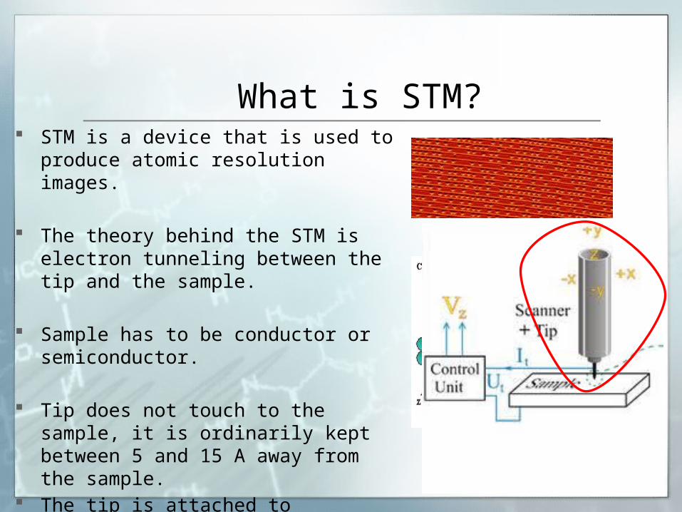
What is STM? STM is a device that is used to produce atomic
resolution images.
The theory behind the STM is electron tunneling between the tip and the sample.
Sample has to be conductor or semiconductor.
Tip does not touch to the sample, it is ordinarily kept between 5 and 15 A away from the sample.
The tip is attached to piezoelectric crystals which, moves the tip on the sample with some electronic feed back control.

Quantum Mechanical Tunneling The electrons, that have particle and wave nature, are
free to move around the metal but cannot leave it. When the cloud of electrons collides with the barrier,
part of the cloud may penetrate the barriers and appear on the other side.
This process is called tunneling because the electron does not have enough kinetic energy to travel over the barrier, but is able to exist on the other side
It is as if the electron found a way to dig a tunnel through the barrier.
A very small current will flow between a sharp metal probe tip and the surface of an electrically conductive material.
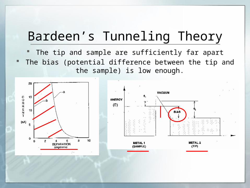
Bardeen’s Tunneling Theory The tip and sample are sufficiently far apart
The bias (potential difference between the tip and the sample) is low enough.
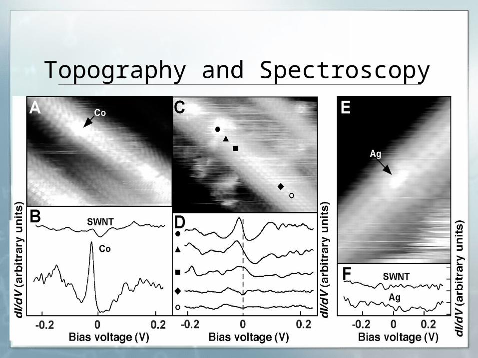
Topography and Spectroscopy
STM characterization of size-selected V1, V2, VO, and VO2 clusters on a TiO2
(110)-(1×1) surface at room temperature
Scott P. Price, Xiao Tong, Claron Ridge, Vladimir Shapovalov, Zhenpeng Hu, Paul Kemper, Horia Metiu, Michael T. Bowers, Steven K. Buratto
Department of Chemistry and Biochemistry, University of California, Santa Barbara, CA 93106-9510, USA
Surface Science 605 (2011)
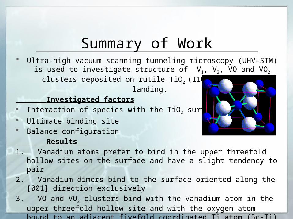
Summary of Work Ultra-high vacuum scanning tunneling microscopy (UHV–STM) is used to investigate structure of V1, V2, VO and VO2 clusters deposited on rutile TiO2 (110)
by ion soft landing.
Investigated factors Interaction of species with the TiO2 surface
Ultimate binding site Balance configuration
Results
1. Vanadium atoms prefer to bind in the upper threefold hollow sites on the surface and have a slight tendency to pair
2. Vanadium dimers bind to the surface oriented along the [001] direction exclusively
3. VO and VO2 clusters bind with the vanadium atom in the upper threefold hollow site and with the oxygen atom bound to an adjacent fivefold coordinated Ti atom (5c-Ti)

Experiments TiO2 Preparation
TiO2(110) samples were cleaned in UHV with several cycles of argon ion bombardment (1 kV) and annealing (~1200 K for 10 s).
Sample cleanliness was verified by STM. Samples were flashed to ~1000 K for several seconds to ensure that surface hydroxyls
were removed. Cluster Preparation Laser is focused onto a rotating, translating
vanadium rod, which generates a plasma of ablated vanadium atoms.
A pulse of argon is introduced into the source, resulting in plasma reactions that cause vanadium and vanadium oxide cluster growth.
Seeding the argon expansion gas with 20% oxygen yields an ion beam composed of VxOy+ ions, as shown in the mass spectrum.
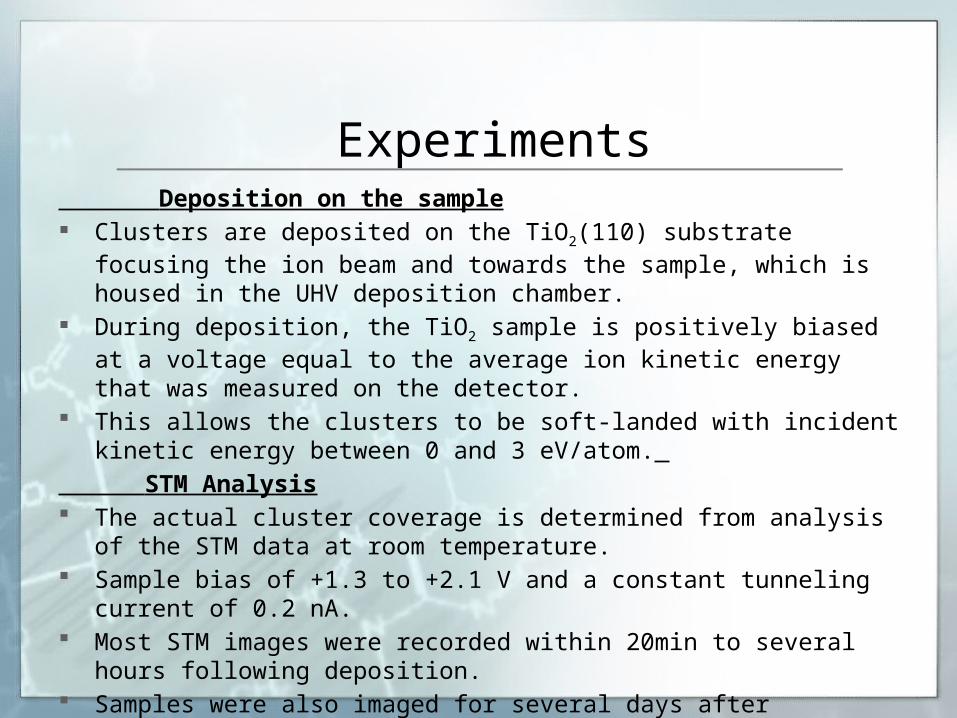
Experiments Deposition on the sample Clusters are deposited on the TiO2(110) substrate focusing the ion beam and towards
the sample, which is housed in the UHV deposition chamber. During deposition, the TiO2 sample is positively biased at a voltage equal to the
average ion kinetic energy that was measured on the detector. This allows the clusters to be soft-landed with incident kinetic energy between 0
and 3 eV/atom.
STM Analysis The actual cluster coverage is determined from analysis of the STM data at room
temperature. Sample bias of +1.3 to +2.1 V and a constant tunneling current of 0.2 nA. Most STM images were recorded within 20min to several hours following
deposition. Samples were also imaged for several days after deposition with no significant
changes in the density or appearance of the clusters.
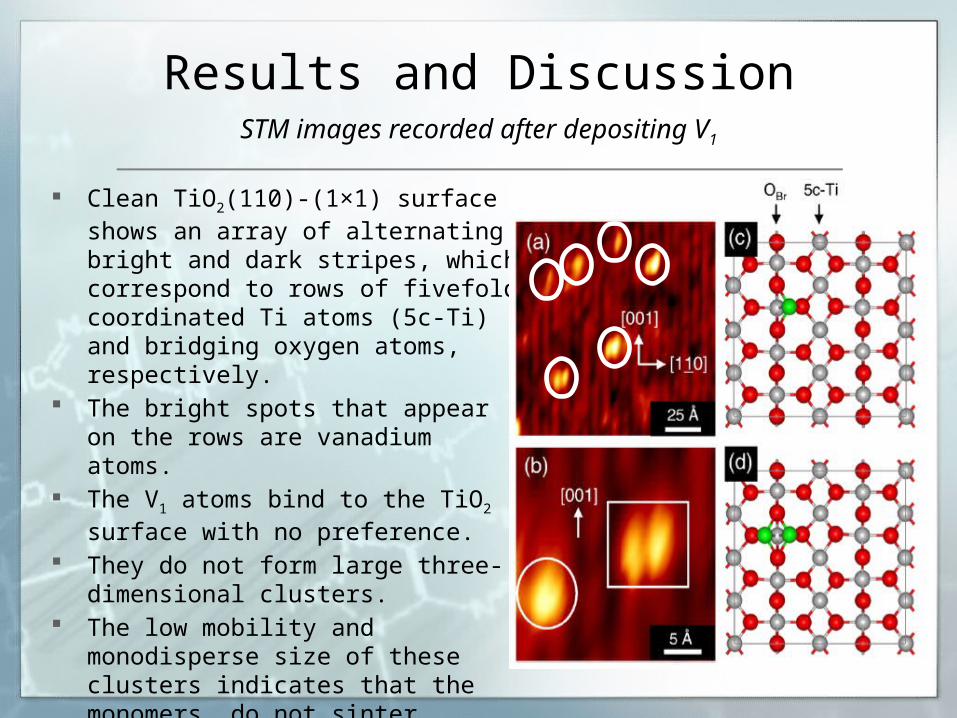
Results and DiscussionSTM images recorded after depositing V1
Clean TiO2(110)-(1×1) surface shows an array of alternating bright and dark stripes, which correspond to rows of fivefold coordinated Ti atoms (5c-Ti) and bridging oxygen atoms, respectively.
The bright spots that appear on the rows are vanadium atoms.
The V1 atoms bind to the TiO2 surface with no preference.
They do not form large three-dimensional clusters.
The low mobility and monodisperse size of these clusters indicates that the monomers do not sinter.
That was attributed to the high reactivity of vanadium with the titania surface.

Results and DiscussionSTM images recorded after depositing V1
The vanadium monomers appear slightly elongated (~9 Å) in the [001] direction and are 1.7 Å in height, indicating that the features are one atomic layer tall.
V1 atoms are positioned between the 5c-Ti and bridging oxygen rows.
Both vanadium atoms are located in upper threefold hollow sites and are separated by a bridging oxygen.
The bonding of the vanadium to these three oxygen atoms, coupled with DFT calculations showing that the vanadium atom transfers electrons to its neighboring oxygen atoms, suggests that this electronic effect is responsible for the observed elongation of the vanadium clusters.
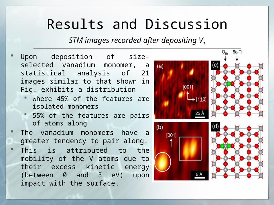
Upon deposition of size-selected vanadium monomer, a statistical analysis of 21 images similar to that shown in Fig. exhibits a distribution where 45% of the features are isolated
monomers 55% of the features are pairs of atoms along
The vanadium monomers have a greater tendency to pair along.
This is attributed to the mobility of the V atoms due to their excess kinetic energy (between 0 and 3 eV) upon impact with the surface.
Results and DiscussionSTM images recorded after depositing V1
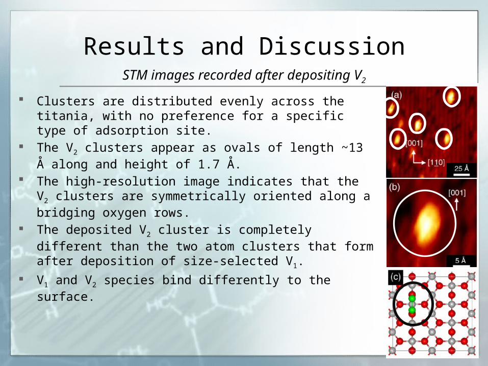
Clusters are distributed evenly across the titania, with no preference for a specific type of adsorption site.
The V2 clusters appear as ovals of length ~13 Å along and height of 1.7 Å.
The high-resolution image indicates that the V2 clusters are symmetrically oriented along a bridging oxygen rows.
The deposited V2 cluster is completely different than the two atom clusters that form after deposition of size-selected V1.
V1 and V2 species bind differently to the surface.
Results and DiscussionSTM images recorded after depositing V2
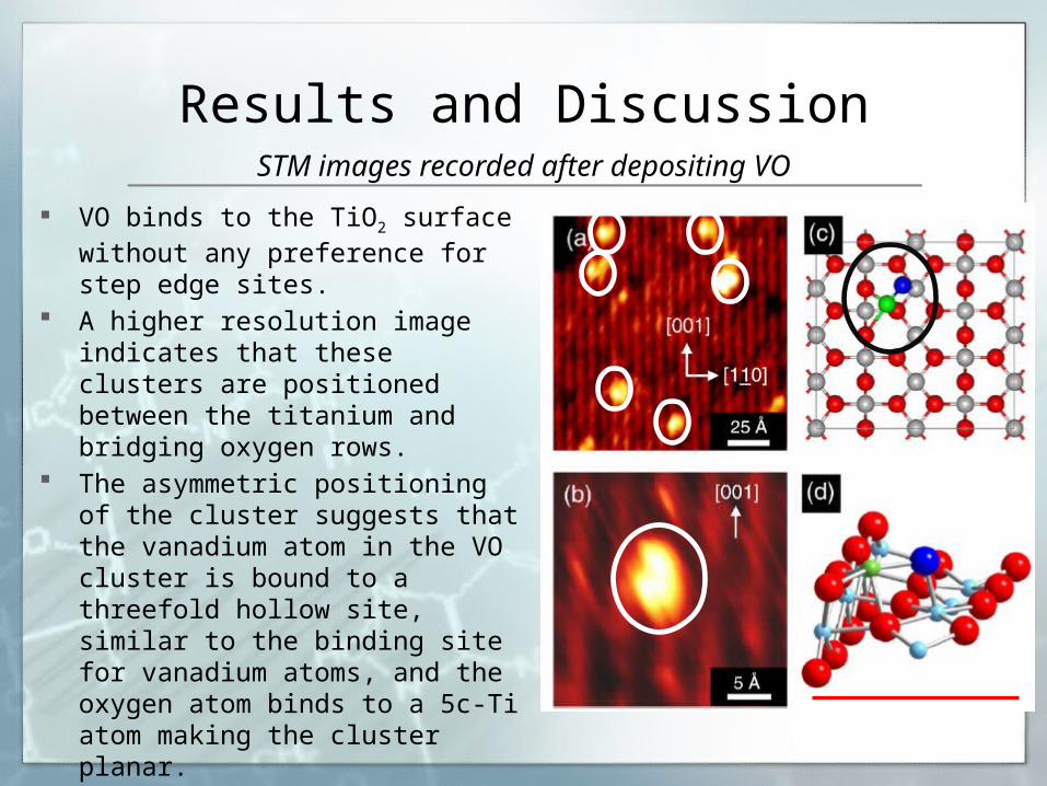
VO binds to the TiO2 surface without any preference for step edge sites.
A higher resolution image indicates that these clusters are positioned between the titanium and bridging oxygen rows.
The asymmetric positioning of the cluster suggests that the vanadium atom in the VO cluster is bound to a threefold hollow site, similar to the binding site for vanadium atoms, and the oxygen atom binds to a 5c-Ti atom making the cluster planar.
Results and DiscussionSTM images recorded after depositing VO
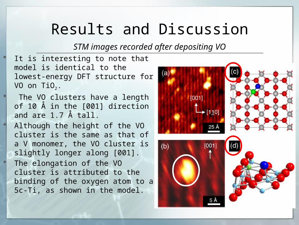
It is interesting to note that model is identical to the lowest-energy DFT structure for VO on TiO2.
The VO clusters have a length of 10 Å in the [001] direction and are 1.7 Å tall.
Although the height of the VO cluster is the same as that of a V monomer, the VO cluster is slightly longer along [001].
The elongation of the VO cluster is attributed to the binding of the oxygen atom to a 5c-Ti, as shown in the model.
Results and DiscussionSTM images recorded after depositing VO
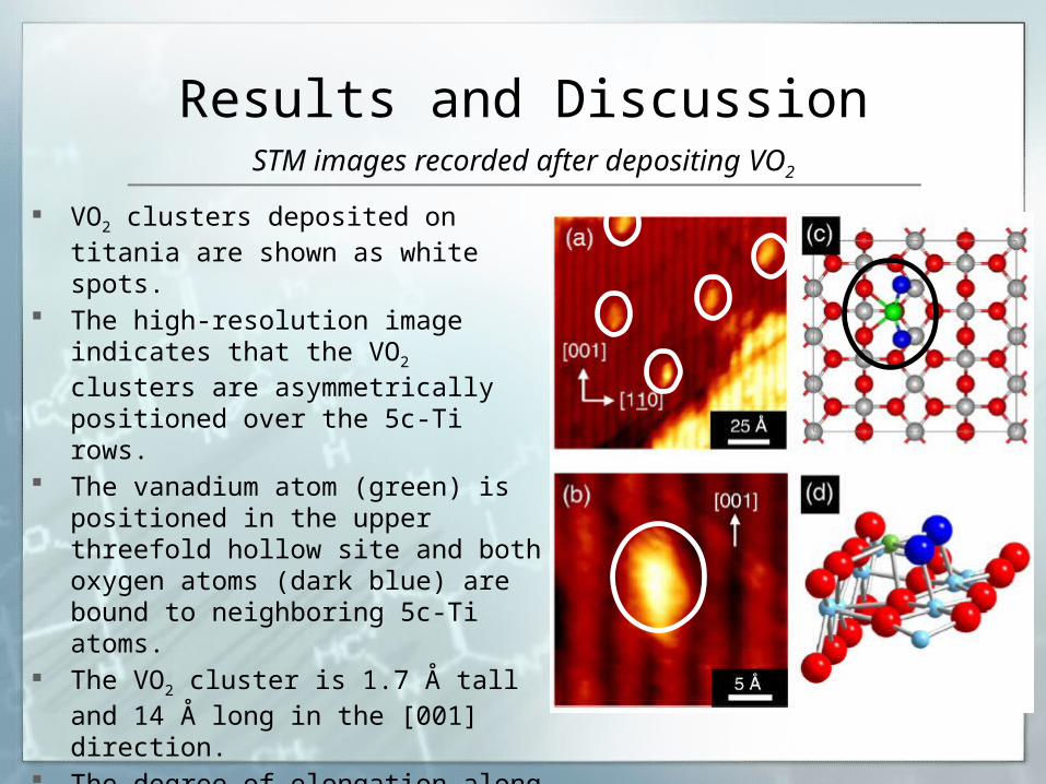
VO2 clusters deposited on titania are shown as white spots.
The high-resolution image indicates that the VO2 clusters are asymmetrically positioned over the 5c-Ti rows.
The vanadium atom (green) is positioned in the upper threefold hollow site and both oxygen atoms (dark blue) are bound to neighboring 5c-Ti atoms.
The VO2 cluster is 1.7 Å tall and 14 Å long in the [001] direction.
The degree of elongation along [001] of VO2 clusters on TiO2(110) is much greater than the VO clusters.
This structure is only 0.25 eV lower in energy than that presented in the DFT model.
Results and DiscussionSTM images recorded after depositing VO2
Conclusion Preferred adsorption sites of V1, V2, VO, and VO2 clusters are determined by using
STM. V1, VO, and VO2 clusters are centered asymmetrically over the 5c-Ti rows and have
varying lengths along the [001] direction. V2 clusters appear symmetrically positioned over the bridging oxygen row.
Comparison of the STM results to DFT calculations determined an atomistic model for these structures.
Direct interactions between metal nanoparticlesand support: STM studies of Pd on TiO2
(1 1 0)
Michael Bowker *, Elodie Fourre´
Wolfson Nanoscience Laboratory, School of Chemistry, Cardiff University, Wales, UK
Applied Surface Science 254 (2008)
Summary of Work Ultra-nanoparticulate model catalysts of Pd had fabricated on TiO2 (1 1 0) using metal
vapour deposition (MVD) to form particles in the size range 1–50 nm. That was imaged at very high spatial resolution (and in some cases at atomic resolution)
using scanning tunnelling microscopy (STM).
Investigated Parameters The atomic level mechanism responsible for certain phenomena in catalysis. Spillover and the so-called strong metal–support interaction (SMSI) effect.
Results Oxygen spillover from Pd particles to the titania support occurs due to the fast adsorption
of oxygen on Pd compared with titania. Ti layers are partially oxidised and form very well defined structures of two main types—
a rectangular lattice and hexagonal unit cells of large dimension. These layers passivate the surface for the adsorption of CO.
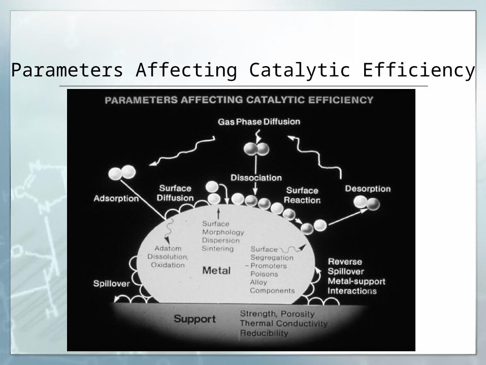
Parameters Affecting Catalytic Efficiency

Fabrication of Model Catalysts Single crystals of titania are used and metal nanoparticles are fabricated onto them by
either evaporation (metal vapour deposition, MVD) or by chemical deposition (metal-organic chemical vapour deposition, MOCVD).
The support must be conductive and vacuum-annealed titania has reasonably good conductivity.
The other approach is the‘inverse catalyst’ methodology, that is, the deposition of thin
layers of support onto a metal substrate; metal nanoparticles may be deposited onto this layer in the same ways as described above.
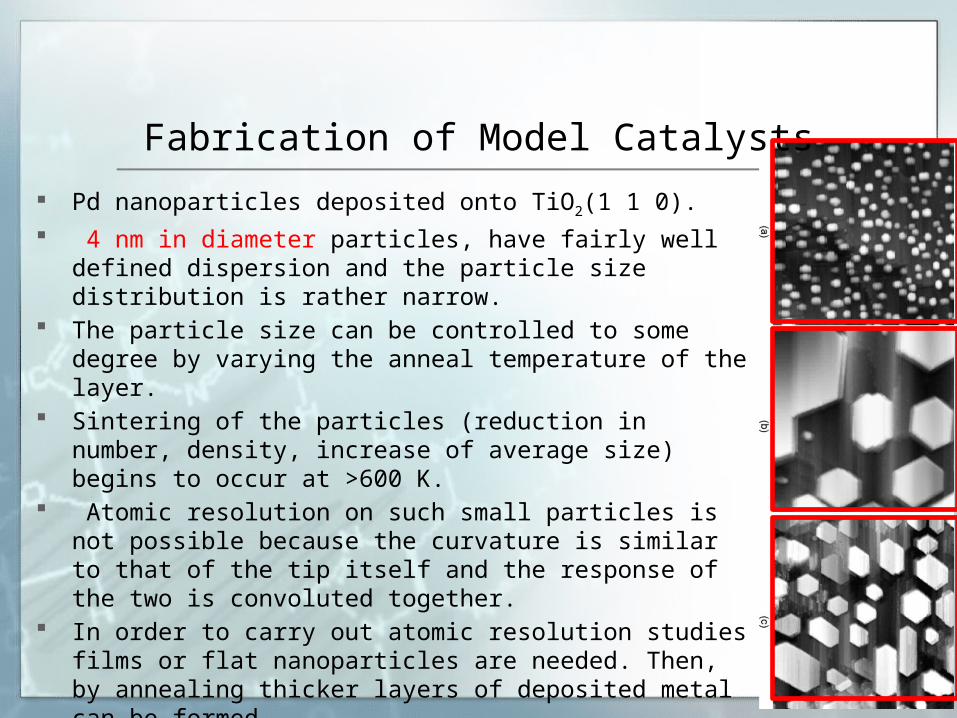
Fabrication of Model Catalysts
Pd nanoparticles deposited onto TiO2(1 1 0).
4 nm in diameter particles, have fairly well defined dispersion and the particle size distribution is rather narrow.
The particle size can be controlled to some degree by varying the anneal temperature of the layer.
Sintering of the particles (reduction in number, density, increase of average size) begins to occur at >600 K.
Atomic resolution on such small particles is not possible because the curvature is similar to that of the tip itself and the response of the two is convoluted together.
In order to carry out atomic resolution studies films or flat nanoparticles are needed. Then, by annealing thicker layers of deposited metal can be formed.
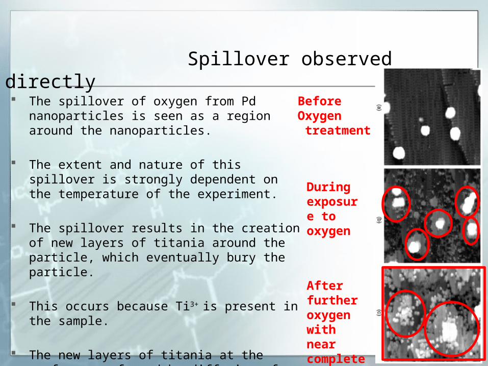
Spillover observed directly The spillover of oxygen from Pd nanoparticles is seen
as a region around the nanoparticles.
The extent and nature of this spillover is strongly dependent on the temperature of the experiment.
The spillover results in the creation of new layers of titania around the particle, which eventually bury the particle.
This occurs because Ti3+ is present in the sample.
The new layers of titania at the surface are formed by diffusion of these interstitials to the surface, which are then oxidised when impacted by gas phase oxygen molecules.
BeforeOxygen treatment
During exposure to oxygen
After furtheroxygen withnear completeEncapsulationof the particle.
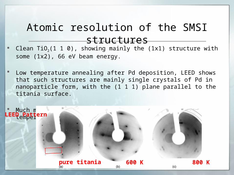
Atomic resolution of the SMSI structures Clean TiO2(1 1 0), showing mainly the (1x1) structure with some (1x2), 66 eV beam
energy.
Low temperature annealing after Pd deposition, LEED shows that such structures are mainly single crystals of Pd in nanoparticle form, with the (1 1 1) plane parallel to the titania surface.
Much more complex LEED patterns are seen after high-temperature annealing
LEED Pattern
pure titania 600 K 800 K
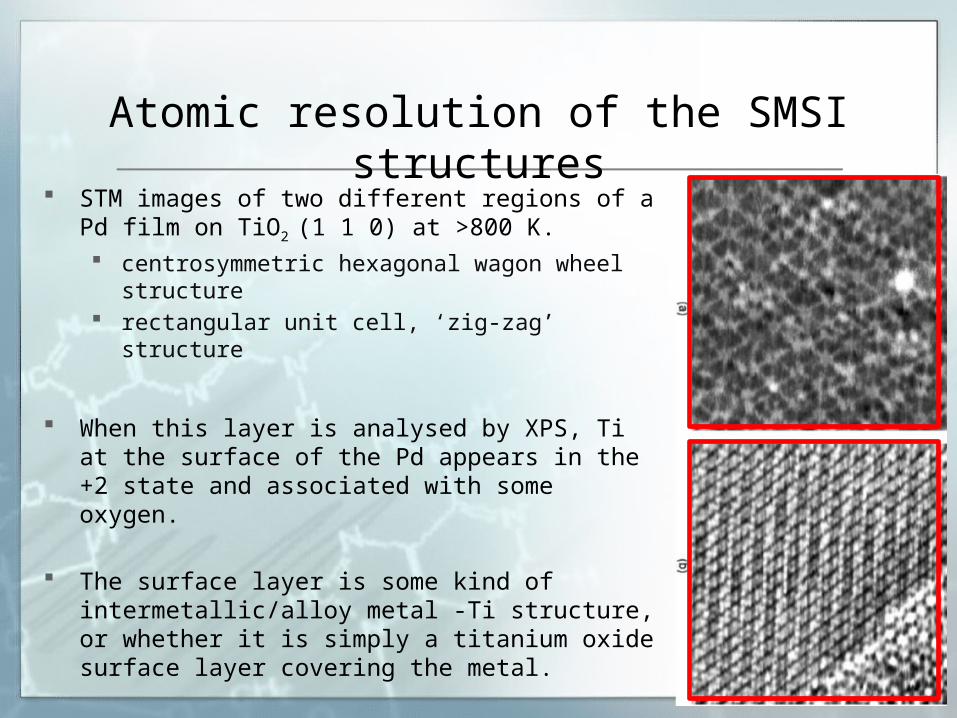
STM images of two different regions of a Pd film on TiO2
(1 1 0) at >800 K. centrosymmetric hexagonal wagon wheel structure rectangular unit cell, ‘zig-zag’ structure
When this layer is analysed by XPS, Ti at the surface of the Pd appears in the +2 state and associated with some oxygen.
The surface layer is some kind of intermetallic/alloy metal -Ti structure, or whether it is simply a titanium oxide surface layer covering the metal.
Atomic resolution of the SMSI structures
Treatment in oxygen at these and higher temperatures leads to the net spillover of oxygen to the adjacent oxide lattice.
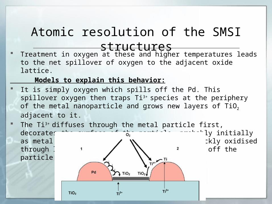
Models to explain this behavior: It is simply oxygen which spills off the Pd. This spillover oxygen then traps Ti3+
species at the periphery of the metal nanoparticle and grows new layers of TiO2 adjacent to it.
The Ti3+ diffuses through the metal particle first, decorates the surface of the particle, probably initially as metal atoms at low temperature, but is quickly oxidised through low oxidation states to finally spill off the particle onto the adjacent support as TiO2.
Atomic resolution of the SMSI structures
Conclusion The resulting surface has been shown to be a complex function of thermal treatment and
redox potential in the gas phase.
Vacuum is effectively a reducing environment because loss of oxygen can occur by desorption from the surface during annealing.
Under such conditions new layers of titanium oxide can form at the surface of the metal nanoparticles.
In oxidising environments spillover of oxygen can occur from the reactive Pd centres to the surrounding oxide, providing the oxide is already in a reduced state.
Catalytic oxidation of graphite by mass-selected ruthenium nanoparticles
S. Murphy, R.M. Nielsen, C. Strebel, M. Johansson, J.H. Nielsen *
Center for Individual Nanoparticle Functionality (CINF), Department of Physics, Technical University of Denmark, 2800 Kongens Lyngby, Denmark
CA R B O N 4 9 ( 2 0 1 1 )

Summary of Work The catalytic oxidation of graphite by mass-selected Ru nanoparticles was studied by
using the scanning tunneling microscopy and temperature programmed oxidation methods.
Channeling by the nanoparticles was observed on the highly-oriented pyrolytic graphite (HOPG) basal surface at temperatures above 750 C.
Ar+ ion bombardment was used to create layers of disordered carbon of various depths on the HOPG surface.
Investigated Parameters
Depths of carbon layers
Channeling propagation rate
Results Larger nanoparticles creates higher channel propagation rate in the carbon layer. The depth of the interface determined whether the nanoparticles etched paths parallel or
perpendicular to the surface. Sputtered surfaces undergoing gasification at much lower temperatures than the
unsputtered surface.
Experiments The experiments were performed in a multichamber ultrahigh vacuum (UHV) system
with a base pressure in the low 10-11 mbar region. HOPG substrates (SPI-1, 7 mm·7mm· 0.5 mm) were cleaved in air and put in radiative
heater about 700 C. The influence of the degree of graphitisation of the support on the oxidation behaviour
was investigated by pre-sputtering the HOPG surfaces with 500 eV Ar+ ions. Pre-formed mass-selected Ru particles were soft-landed onto the HOPG substrates at
room temperature using an inert gas-aggregation source. The particles are formed by gas-phase condensation from a flux of Ru atoms that are
sputtered from a 99.99% pure Ru target using a magnetron sputter source (B). The cooled argon gas thermalises the sputtered Ru atoms so that they condense into
clusters, which further coalesce to form nanoparticles.
Experiments Ruthenium nanoparticles are applied as a beam to the substrate. The substrate is placed at a small positive bias (36 V) so that negatively charged
nanoparticles are soft-landed onto the surface. Ion scattering spectroscopy (ISS) measurements were used to confirm the surface
cleanliness of the deposited particles. TPO experiments were performed by backfilling the UHV chamber with high purity O2.
The sample temperature was ramped at a rate of 1 C/s in the oxygen atmosphere. The local gas composition evolved at the surface during the temperature ramp was
monitored using a mass spectrometer. STM was performed at room temperature in constant current mode. SEM and TEM analysis of the nanoparticles.

ResultsMass-selected Ru nanoparticles
Approximately 10% of the surface is covered by nanoparticles after deposition of 8.4 nm Ru nanoparticles onto a HOPG surface that had been sputtered for 30 s.
The ISS shows a ruthenium peak at 865 eV and a broad carbon peak at around 300 eV.
Degree of cleanliness of the as-deposited nanoparticles is high beacouse only carbon and Ru picks are observed.
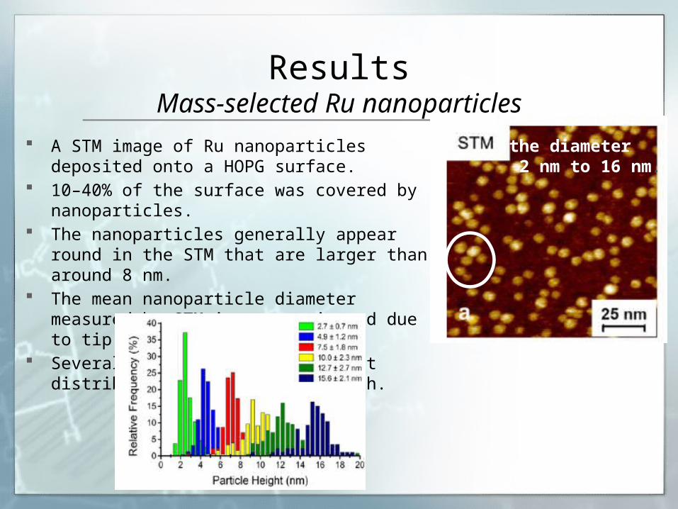
A STM image of Ru nanoparticles deposited onto a HOPG surface.
10–40% of the surface was covered by nanoparticles. The nanoparticles generally appear round in the STM
that are larger than around 8 nm. The mean nanoparticle diameter measured by STM is
overestimated due to tip convolution effects. Several of these particle height distributions are shown
in graph.
ResultsMass-selected Ru nanoparticles
the diameter 2 nm to 16 nm.

TEM images shows that the nanoparticles are not homogeneous.
They display a range of different polymorphs especially for larger nanoparticles.
Good agreement was obtained between the particle diameter distributions measured by TEM and height distribution in STM.
ResultsMass-selected Ru nanoparticles
6 nm 12 nm 16 nm

TPO measurements were performed to investigate the support oxidation process.
These were performed by heating linearly to 770 C in 106 mbar O2.
CO, CO2 and O2 signals measured above the sample surface during oxidation of a sputtered HOPG surface 15% covered by 2.3 nm Ru nanoparticles.
The CO signal continues to rise for some temperature interval above Ti (ignition temp.), before reaching a peak value at Tp.
ResultsTemperature programmed oxidation
When TPO measurements were performed on HOPG surfaces without nanoparticles the CO background did not rise, indicating that the oxidation process is catalysed by the Ru nanoparticles.
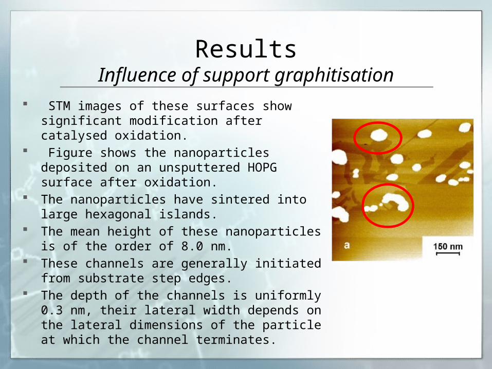
STM images of these surfaces show significant modification after catalysed oxidation.
Figure shows the nanoparticles deposited on an unsputtered HOPG surface after oxidation.
The nanoparticles have sintered into large hexagonal islands.
The mean height of these nanoparticles is of the order of 8.0 nm.
These channels are generally initiated from substrate step edges.
The depth of the channels is uniformly 0.3 nm, their lateral width depends on the lateral dimensions of the particle at which the channel terminates.
ResultsInfluence of support graphitisation
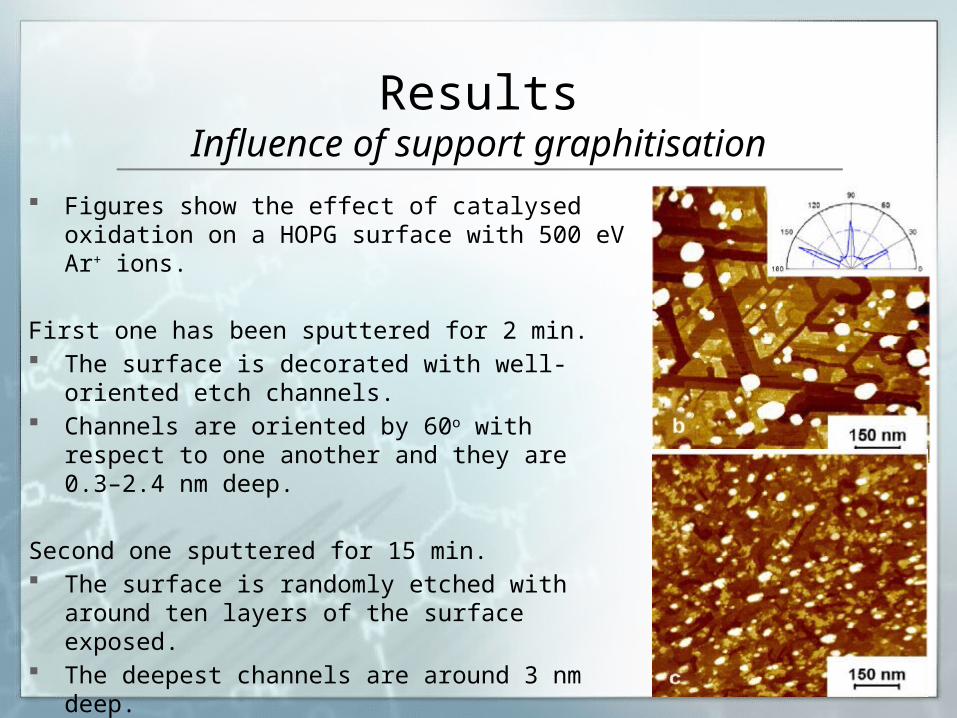
Figures show the effect of catalysed oxidation on a HOPG surface with 500 eV Ar+ ions.
First one has been sputtered for 2 min. The surface is decorated with well-oriented etch channels. Channels are oriented by 60o with respect to one another
and they are 0.3–2.4 nm deep.
Second one sputtered for 15 min. The surface is randomly etched with around ten layers of
the surface exposed. The deepest channels are around 3 nm deep.
ResultsInfluence of support graphitisation
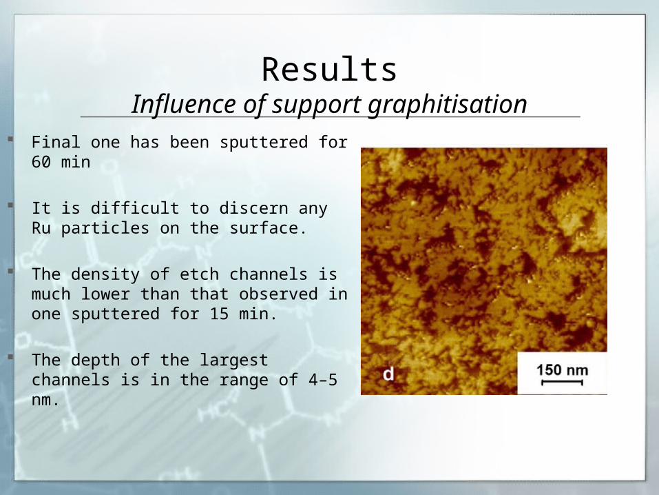
Final one has been sputtered for 60 min
It is difficult to discern any Ru particles on the surface.
The density of etch channels is much lower than that observed in one sputtered for 15 min.
The depth of the largest channels is in the range of 4–5 nm.
ResultsInfluence of support graphitisation
Conclusion Ar+ ion bombardment can be used to create a layer of disordered carbon with
controlled thickness on the HOPG surface.
The etch channels are highly directional when the nanoparticles are in contact with the graphite basal plane.
The gasification temperature depends on the degree of graphitisation of the support.

Thank you for your listening
Related Documents