This is advance information on a new product now in development or undergoing evaluation. Details are subject to change without notice 21 July 2000 CONF I DENT IA L ® 7110599 B 1 Introduction . . . . . . . . . . . . . . . . . . . . . . . . . . . . . . . . . . . . . . . . . . . . . . . . . . . . . . . . . . . . . . . . . . . . . . . . . . 2 2 Register map . . . . . . . . . . . . . . . . . . . . . . . . . . . . . . . . . . . . . . . . . . . . . . . . . . . . . . . . . . . . . . . . . . . . . . . . . 4 3 Asynchronous serial controller (ASC) registers . . . . . . . . . . . . . . . . . . . . . . . . . . . . . . . . . . . . . . . . . . . . . . . 23 4 Audio MPEG (AUD) registers . . . . . . . . . . . . . . . . . . . . . . . . . . . . . . . . . . . . . . . . . . . . . . . . . . . . . . . . . . . . 31 5 Block move DMA (BMDMA) registers . . . . . . . . . . . . . . . . . . . . . . . . . . . . . . . . . . . . . . . . . . . . . . . . . . . . . . 46 6 Cache control registers . . . . . . . . . . . . . . . . . . . . . . . . . . . . . . . . . . . . . . . . . . . . . . . . . . . . . . . . . . . . . . . . . 47 7 Configuration and control (CFG) registers . . . . . . . . . . . . . . . . . . . . . . . . . . . . . . . . . . . . . . . . . . . . . . . . . . . 50 8 Clock generator (CKG) registers . . . . . . . . . . . . . . . . . . . . . . . . . . . . . . . . . . . . . . . . . . . . . . . . . . . . . . . . . . 53 9 Digital encoder registers . . . . . . . . . . . . . . . . . . . . . . . . . . . . . . . . . . . . . . . . . . . . . . . . . . . . . . . . . . . . . . . . 58 10 External memory interface (EMI) registers . . . . . . . . . . . . . . . . . . . . . . . . . . . . . . . . . . . . . . . . . . . . . . . . . . 74 11 Interrupt controller registers . . . . . . . . . . . . . . . . . . . . . . . . . . . . . . . . . . . . . . . . . . . . . . . . . . . . . . . . . . . . . . 81 12 Interrupt level controller registers . . . . . . . . . . . . . . . . . . . . . . . . . . . . . . . . . . . . . . . . . . . . . . . . . . . . . . . . . 86 13 MPEG DMA controller registers . . . . . . . . . . . . . . . . . . . . . . . . . . . . . . . . . . . . . . . . . . . . . . . . . . . . . . . . . . 87 14 PES parser (PES) registers . . . . . . . . . . . . . . . . . . . . . . . . . . . . . . . . . . . . . . . . . . . . . . . . . . . . . . . . . . . . . . 89 15 Parallel input/output (PIO) registers . . . . . . . . . . . . . . . . . . . . . . . . . . . . . . . . . . . . . . . . . . . . . . . . . . . . . . . 92 16 PWM and counter module registers . . . . . . . . . . . . . . . . . . . . . . . . . . . . . . . . . . . . . . . . . . . . . . . . . . . . . . . 97 17 SmartCard interface (Sc) registers . . . . . . . . . . . . . . . . . . . . . . . . . . . . . . . . . . . . . . . . . . . . . . . . . . . . . . . . 103 18 Sub-picture decoder (SPD) registers . . . . . . . . . . . . . . . . . . . . . . . . . . . . . . . . . . . . . . . . . . . . . . . . . . . . . . . 104 19 Synchronous serial controller (SSC) registers . . . . . . . . . . . . . . . . . . . . . . . . . . . . . . . . . . . . . . . . . . . . . . . . 112 20 Transport stream demultiplexor registers . . . . . . . . . . . . . . . . . . . . . . . . . . . . . . . . . . . . . . . . . . . . . . . . . . . 117 21 Teletext interface (Ttxt) registers . . . . . . . . . . . . . . . . . . . . . . . . . . . . . . . . . . . . . . . . . . . . . . . . . . . . . . . . . . 127 22 SDRAM block move (USD) registers . . . . . . . . . . . . . . . . . . . . . . . . . . . . . . . . . . . . . . . . . . . . . . . . . . . . . . . 130 23 Video decoder (VID) registers . . . . . . . . . . . . . . . . . . . . . . . . . . . . . . . . . . . . . . . . . . . . . . . . . . . . . . . . . . . . 131 24 Index of Registers . . . . . . . . . . . . . . . . . . . . . . . . . . . . . . . . . . . . . . . . . . . . . . . . . . . . . . . . . . . . . . . . . . . . . 158 25 Revision history . . . . . . . . . . . . . . . . . . . . . . . . . . . . . . . . . . . . . . . . . . . . . . . . . . . . . . . . . . . . . . . . . . . . . . . 160 REGISTER MANUAL STi5500

Welcome message from author
This document is posted to help you gain knowledge. Please leave a comment to let me know what you think about it! Share it to your friends and learn new things together.
Transcript
This is advance information on a new product now in development or undergoing evaluation. Details are subject to change without notice
21 July 2000
CONFIDENTIAL®
7110599 B
1 Introduction . . . . . . . . . . . . . . . . . . . . . . . . . . . . . . . . . . . . . . . . . . . . . . . . . . . . . . . . . . . . . . . . . . . . . . . . . . 2
2 Register map . . . . . . . . . . . . . . . . . . . . . . . . . . . . . . . . . . . . . . . . . . . . . . . . . . . . . . . . . . . . . . . . . . . . . . . . . 4
3 Asynchronous serial controller (ASC) registers . . . . . . . . . . . . . . . . . . . . . . . . . . . . . . . . . . . . . . . . . . . . . . . 23
4 Audio MPEG (AUD) registers . . . . . . . . . . . . . . . . . . . . . . . . . . . . . . . . . . . . . . . . . . . . . . . . . . . . . . . . . . . . 31
5 Block move DMA (BMDMA) registers . . . . . . . . . . . . . . . . . . . . . . . . . . . . . . . . . . . . . . . . . . . . . . . . . . . . . . 46
6 Cache control registers . . . . . . . . . . . . . . . . . . . . . . . . . . . . . . . . . . . . . . . . . . . . . . . . . . . . . . . . . . . . . . . . . 47
7 Configuration and control (CFG) registers . . . . . . . . . . . . . . . . . . . . . . . . . . . . . . . . . . . . . . . . . . . . . . . . . . . 50
8 Clock generator (CKG) registers . . . . . . . . . . . . . . . . . . . . . . . . . . . . . . . . . . . . . . . . . . . . . . . . . . . . . . . . . . 53
9 Digital encoder registers . . . . . . . . . . . . . . . . . . . . . . . . . . . . . . . . . . . . . . . . . . . . . . . . . . . . . . . . . . . . . . . . 58
10 External memory interface (EMI) registers . . . . . . . . . . . . . . . . . . . . . . . . . . . . . . . . . . . . . . . . . . . . . . . . . . 74
11 Interrupt controller registers . . . . . . . . . . . . . . . . . . . . . . . . . . . . . . . . . . . . . . . . . . . . . . . . . . . . . . . . . . . . . . 81
12 Interrupt level controller registers . . . . . . . . . . . . . . . . . . . . . . . . . . . . . . . . . . . . . . . . . . . . . . . . . . . . . . . . . 86
13 MPEG DMA controller registers . . . . . . . . . . . . . . . . . . . . . . . . . . . . . . . . . . . . . . . . . . . . . . . . . . . . . . . . . . 87
14 PES parser (PES) registers . . . . . . . . . . . . . . . . . . . . . . . . . . . . . . . . . . . . . . . . . . . . . . . . . . . . . . . . . . . . . . 89
15 Parallel input/output (PIO) registers . . . . . . . . . . . . . . . . . . . . . . . . . . . . . . . . . . . . . . . . . . . . . . . . . . . . . . . 92
16 PWM and counter module registers . . . . . . . . . . . . . . . . . . . . . . . . . . . . . . . . . . . . . . . . . . . . . . . . . . . . . . . 97
17 SmartCard interface (Sc) registers . . . . . . . . . . . . . . . . . . . . . . . . . . . . . . . . . . . . . . . . . . . . . . . . . . . . . . . . 103
18 Sub-picture decoder (SPD) registers . . . . . . . . . . . . . . . . . . . . . . . . . . . . . . . . . . . . . . . . . . . . . . . . . . . . . . . 104
19 Synchronous serial controller (SSC) registers . . . . . . . . . . . . . . . . . . . . . . . . . . . . . . . . . . . . . . . . . . . . . . . . 112
20 Transport stream demultiplexor registers . . . . . . . . . . . . . . . . . . . . . . . . . . . . . . . . . . . . . . . . . . . . . . . . . . . 117
21 Teletext interface (Ttxt) registers . . . . . . . . . . . . . . . . . . . . . . . . . . . . . . . . . . . . . . . . . . . . . . . . . . . . . . . . . . 127
22 SDRAM block move (USD) registers . . . . . . . . . . . . . . . . . . . . . . . . . . . . . . . . . . . . . . . . . . . . . . . . . . . . . . . 130
23 Video decoder (VID) registers . . . . . . . . . . . . . . . . . . . . . . . . . . . . . . . . . . . . . . . . . . . . . . . . . . . . . . . . . . . . 131
24 Index of Registers . . . . . . . . . . . . . . . . . . . . . . . . . . . . . . . . . . . . . . . . . . . . . . . . . . . . . . . . . . . . . . . . . . . . . 158
25 Revision history . . . . . . . . . . . . . . . . . . . . . . . . . . . . . . . . . . . . . . . . . . . . . . . . . . . . . . . . . . . . . . . . . . . . . . . 160
REGISTER MANUAL
STi5500
L1 - Introduction STi5500
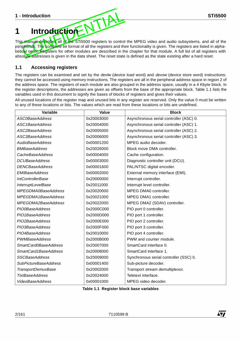
CONFIDENTIA1 IntroductionThis manual describes all of the STi5500 registers to control the MPEG video and audio subsystems, and all of theperipherals. The complete bit format of all the registers and their functionality is given. The registers are listed in alpha-betical order. Registers for other modules are described in the chapter for that module. A full list of all registers withabsolute addresses is given in the data sheet. The reset state is defined as the state existing after a hard reset.
1.1 Accessing registersThe registers can be examined and set by the devlw (device load word) and devsw (device store word) instructions;they cannot be accessed using memory instructions. The registers are all in the peripheral address space in region 2 ofthe address space. The registers of each module are also grouped in the address space, usually in a 4 Kbyte block. Inthe register descriptions, the addresses are given as offsets from the base of the appropriate block. Table 1.1 lists thevariables used in this document to signify the bases of blocks of registers and gives their values.All unused locations of the register map and unused bits in any register are reserved. Only the value 0 must be writtento any of these locations or bits. The values which are read from these locations or bits are undefined.
Variable Value Block
ASC0BaseAddress 0x20003000 Asynchronous serial controller (ASC) 0.
ASC1BaseAddress 0x20004000 Asynchronous serial controller (ASC) 1.
ASC2BaseAddress 0x20005000 Asynchronous serial controller (ASC) 2.
ASC3BaseAddress 0x20006000 Asynchronous serial controller (ASC) 3.
AudioBaseAddress 0x00001200 MPEG audio decoder.
BMBaseAddress 0x20026000 Block move DMA controller.
CacheBaseAddress 0x00004000 Cache configuration.
DCUBaseAddress 0x00003000 Diagnostic controller unit (DCU).
DENCBaseAddress 0x00001600 PAL/NTSC digital encoder.
EMIBaseAddress 0x00002000 External memory interface (EMI).
IntControllerBase 0x20000000 Interrupt controller.
InterruptLevelBase 0x20011000 Interrupt level controller.
MPEGDMA0BaseAddress 0x20020000 MPEG DMA0 controller.
MPEGDMA1BaseAddress 0x20021000 MPEG DMA1 controller.
MPEGDMA2BaseAddress 0x20022000 MPEG DMA2 (SDAV) controller.
PIO0BaseAddress 0x2000C000 PIO port 0 controller.
PIO1BaseAddress 0x2000D000 PIO port 1 controller.
PIO2BaseAddress 0x2000E000 PIO port 2 controller.
PIO3BaseAddress 0x2000F000 PIO port 3 controller.
PIO4BaseAddress 0x20010000 PIO port 4 controller.
PWMBaseAddress 0x2000B000 PWM and counter module.
SmartCard0BaseAddress 0x20007000 SmartCard interface 0.
SmartCard1BaseAddress 0x20008000 SmartCard interface 1.
SSCBaseAddress 0x20009000 Synchronous serial controller (SSC) 0.
SubPictureBaseAddress 0x00001400 Sub-picture decoder.
TransportDemuxBase 0x20002000 Transport stream demultiplexor.
TtxtBaseAddress 0x20024000 Teletext interface.
VideoBaseAddress 0x00001000 MPEG video decoder.
Table 1.1 Register block base variables
2/161 7110599 B

LSTi5500 1 - Introduction
CONFIDENTIA1.1.1 Video and audio register addressing
The four subsystems audio, DENC, sub-picture and video, are each allocated a 2 Kbyte block of addresses in the inter-nal peripheral address space. Within these register blocks, bits 7 and 8 are used to define the number of wait statesused when accessing the registers. Table 1.2 shows the values to add to the register addresses for different numbersof wait states.
For example, the audio register AUD_BBE is listed at address 0x70, and is in the audio block, base address0x00001200. To access this register when 3 wait states are needed, the full address is given by:
1.2 Synchronization of video decoder registersThere are two types of video decoder register: synchronized and unsynchronized.Synchronized registers only change value in response to an internal event, either DSYNC or VSYNC, depending onthe register. These registers are double-banked; during the write cycle the new value is loaded into a master register,and on the occurrence of the synchronizing event this value is loaded into a slave register, at which time the new valueis available to the circuit. If a synchronized register is read, the value returned is that held in the master register.Unsynchronized registers change their value immediately they are written to.Some registers are non synchronized registers with edge triggered write (on end of write cycle). This is to avoidglitches on internal signals during write cycles.
Wait states Bit 7 Bit 8 Add to address
3 wait states 1 0 0x080
4 wait states 0 1 0x100
5 wait states 1 1 0x180
Table 1.2 Wait state encoding
FullAddress = 0x70 + WaitStateCode + AudioBaseAddress= 0x70 + 0x080 + 0x00001200= 0x000012F0
7110599 B 3/161
L2 - Register map STi5500
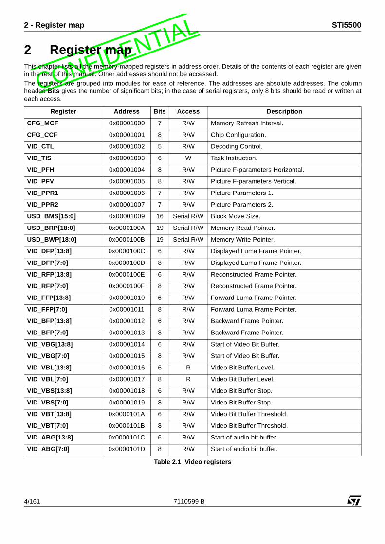
CONFIDENTIA2 Register mapThis chapter lists all the memory-mapped registers in address order. Details of the contents of each register are givenin the rest of this manual. Other addresses should not be accessed. The registers are grouped into modules for ease of reference. The addresses are absolute addresses. The columnheaded Bits gives the number of significant bits; in the case of serial registers, only 8 bits should be read or written ateach access.
Register Address Bits Access Description
CFG_MCF 0x00001000 7 R/W Memory Refresh Interval.
CFG_CCF 0x00001001 8 R/W Chip Configuration.
VID_CTL 0x00001002 5 R/W Decoding Control.
VID_TIS 0x00001003 6 W Task Instruction.
VID_PFH 0x00001004 8 R/W Picture F-parameters Horizontal.
VID_PFV 0x00001005 8 R/W Picture F-parameters Vertical.
VID_PPR1 0x00001006 7 R/W Picture Parameters 1.
VID_PPR2 0x00001007 7 R/W Picture Parameters 2.
USD_BMS[15:0] 0x00001009 16 Serial R/W Block Move Size.
USD_BRP[18:0] 0x0000100A 19 Serial R/W Memory Read Pointer.
USD_BWP[18:0] 0x0000100B 19 Serial R/W Memory Write Pointer.
VID_DFP[13:8] 0x0000100C 6 R/W Displayed Luma Frame Pointer.
VID_DFP[7:0] 0x0000100D 8 R/W Displayed Luma Frame Pointer.
VID_RFP[13:8] 0x0000100E 6 R/W Reconstructed Frame Pointer.
VID_RFP[7:0] 0x0000100F 8 R/W Reconstructed Frame Pointer.
VID_FFP[13:8] 0x00001010 6 R/W Forward Luma Frame Pointer.
VID_FFP[7:0] 0x00001011 8 R/W Forward Luma Frame Pointer.
VID_BFP[13:8] 0x00001012 6 R/W Backward Frame Pointer.
VID_BFP[7:0] 0x00001013 8 R/W Backward Frame Pointer.
VID_VBG[13:8] 0x00001014 6 R/W Start of Video Bit Buffer.
VID_VBG[7:0] 0x00001015 8 R/W Start of Video Bit Buffer.
VID_VBL[13:8] 0x00001016 6 R Video Bit Buffer Level.
VID_VBL[7:0] 0x00001017 8 R Video Bit Buffer Level.
VID_VBS[13:8] 0x00001018 6 R/W Video Bit Buffer Stop.
VID_VBS[7:0] 0x00001019 8 R/W Video Bit Buffer Stop.
VID_VBT[13:8] 0x0000101A 6 R/W Video Bit Buffer Threshold.
VID_VBT[7:0] 0x0000101B 8 R/W Video Bit Buffer Threshold.
VID_ABG[13:8] 0x0000101C 6 R/W Start of audio bit buffer.
VID_ABG[7:0] 0x0000101D 8 R/W Start of audio bit buffer.
Table 2.1 Video registers
4/161 7110599 B

LSTi5500 2 - Register map
CONFIDENTIAVID_ABL[13:8] 0x0000101E 6 R Audio Bit Buffer Level.
VID_ABL[7:0] 0x0000101F 8 R Audio Bit Buffer Level.
VID_ABS[13:8] 0x00001020 6 R/W Audio Bit Buffer Stop.
VID_ABS[7:0] 0x00001021 8 R/W Audio Bit Buffer Stop.
VID_ABT[13:8] 0x00001022 6 R/W Audio Bit Buffer Threshold.
VID_ABT[7:0] 0x00001023 8 R/W Audio Bit Buffer Threshold.
VID_DFS 0x00001024 15 Serial R/W Decoded Frame Size.
VID_DFW 0x00001025 8 R/W Decoded Frame Width.
VID_XFW 0x00001028 8 R/W Displayed Frame Width.
VID_SCN 0x00001029 6 R/W Scan vector
VID_OTP 0x0000102A 14 Serial R/W OSD Top Field Pointer.
VID_OBP 0x0000102B 14 Serial R/W OSD Bottom Field Pointer.
VID_PAN[10:8] 0x0000102C 3 R/W Pan/Scan Horizontal Vector Integer Part.
VID_PAN[7:0] 0x0000102D 8 R/W Pan/Scan Horizontal Vector Integer Part.
VID_PTH[13:8] 0x0000102E 6 R/W Panic threshold.
VID_PTH[7:0] 0x0000102F 8 R/W Panic threshold.
CKG_PLL 0x00001030 7 R/W Clock Generator PLL Parameters.
CKG_CFG 0x00001031 7 R/W Clock Generator Configuration.
CKG_SMC 0x00001032 28 Serial R/W Smart-Card Clock Divider.
CKG_LNK 0x00001033 28 Serial R/W Link Clock Divider.
CKG_PXC 0x00001034 28 Serial R/W Pixel Clock Divider.
CKG_PCM 0x00001035 28 Serial R/W Pcm Clock Divider.
CKG_MCK 0x00001036 28 Serial R/W Sdram Clock Divider.
CKG_AUX 0x00001037 28 Serial R/W Auxiliary Clock Divider.
CFG_DRC 0x00001038 6 R/W DRAM Configuration.
VID_RSTV 0x00001039 1 R/W Video reset
CFG_GCF 0x0000103A 7 R/W General Configuration.
VID_STA1 0x0000103B 8 R Status.
VID_ITM1 0x0000103C 8 R/W Interrupt Mask.
VID_ITS1 0x0000103D 8 R Interrupt Status.
VID_OSD 0x0000103E 7 R/W On-screen Display Configuration.
VID_LDP 0x0000103F 1 R/W Load Pointer.
PES_CF1 0x00001040 8 R/W PES Audio Decoding Control.
PES_CF2 0x00001041 8 R/W PES Video Parser Control.
PES_TM1 0x00001042 8 R DSM Trick Mode.
Register Address Bits Access Description
Table 2.1 Video registers
7110599 B 5/161

L2 - Register map STi5500
CONFIDENTIAPES_TM2 0x00001043 2 R PES Parser Status.
CFG_CDR 0x00001044 8 W Compressed Data Input.
VID_FRZ 0x00001045 1 R/W Freeze Display.
PES_TS[7:0] 0x00001049 8 R PES Time Stamps.
PES_TS[15:8] 0x0000104A 8 R PES Time Stamps.
PES_TS[23:16] 0x0000104B 8 R PES Time Stamps.
PES_TS[31:24] 0x0000104C 8 R PES Time Stamps.
PES_TS[33:32] 0x0000104D 2 R PES Time Stamps.
VID_SPRead 0x0000104E 19 Serial R/W Sub-picture Read Pointer.
VID_SPWrite 0x0000104F 19 Serial R/W Sub-picture Write Pointer.
VID_SPB[10:8] 0x00001050 3 R/W Sub-picture Buffer Begin.
VID_SPB[7:0] 0x00001051 8 R/W Sub-picture Buffer Begin.
VID_SPE[10:8] 0x00001052 3 R/W Sub-picture Buffer End.
VID_SPE[7:0] 0x00001053 8 R/W Sub-picture Buffer End.
VID_VFL 0x00001054 5 R/W Luma vertical filter
VID_VFC 0x00001055 5 R/W Chroma vertical filter
VID_TRF[11:8] 0x00001056 4 R/W Temporal Reference.
VID_TRF[7:0] 0x00001057 8 R/W Temporal Reference.
VID_DFC[13:8] 0x00001058 6 R/W Displayed Chroma Frame Pointer.
VID_DFC[7:0] 0x00001059 8 R/W Displayed Chroma Frame Pointer.
VID_RFC[13:8] 0x0000105A 6 R/W Reconstructed Chroma Frame Pointer.
VID_RFC[7:0] 0x0000105B 8 R/W Reconstructed Chroma Frame Pointer.
VID_FFC[13:8] 0x0000105C 6 R/W Forward Chroma Frame Pointer.
VID_FFC[7:0] 0x0000105D 8 R/W Forward Chroma Frame Pointer.
VID_BFC[13:8] 0x0000105E 6 R/W Backward Chroma Pointer.
VID_BFC[7:0] 0x0000105F 8 R/W Backward Chroma Pointer.
VID_ITM2 0x00001060 8 R/W Interrupt Mask.
VID_ITM3 0x00001061 8 R/W Interrupt Mask.
VID_ITS2 0x00001062 8 R Interrupt Status.
VID_ITS3 0x00001063 8 R Interrupt Status.
VID_STA2 0x00001064 8 R Status.
VID_STA3 0x00001065 8 R Status.
VID_HDF 0x00001066 16 Serial R Header Data FIFO.
VID_CDcount 0x00001067 24 Serial R Bit Buffer Input Counter.
VID_SCDcount 0x00001068 24 Serial R Bit Buffer Output Counter.
Register Address Bits Access Description
Table 2.1 Video registers
6/161 7110599 B

LSTi5500 2 - Register map
CONFIDENTIAVID_HDS 0x00001069 4 R/W Header Search.
VID_LSO 0x0000106A 8 R/W SRC Luminance Offset.
VID_LSR 0x0000106B 8 R/W SRC Luma Resolution.
VID_CSO 0x0000106C 8 R/W SRC Chrominance Offset.
VID_CSR 0x0000106D 8 R/W SRC Chrominance Resolution.
VID_YDO 0x0000106E 8 R/W Display Y Offset.
VID_YDS 0x0000106F 8 R/W Display Y End.
VID_XDO[9:8] 0x00001070 2 R/W Display X Offset.
VID_XDO[7:0] 0x00001071 8 R/W Display X Offset.
VID_XDS[9:8] 0x00001072 2 R/W Display X End.
VID_XDS[7:0] 0x00001073 8 R/W Display X End.
VID_DCF[14:7] 0x00001074 5 R/W Display Configuration.
VID_DCF[6:0] 0x00001075 6 R/W Display Configuration.
VID_QMW 0x00001076 8 W Quantization Matrix Data.
VID_REV 0x00001078 8 R STi5500 Revision.
VID_RSTA 0x0000107A 1 R/W Audio reset
VID_NWM 0x0000107B 1 R/W Not-writable-register mode
VID_END 0x0000107C 1 R/W Little endian - big endian conversion
Register Address Bits Access Description
Table 2.1 Video registers
7110599 B 7/161

L2 - Register map STi5500
CONFIDENTIARegister Address Bits Access Description
AUD_ANC[7:0] 0x00001206 8 R Ancillary Data Buffer.
AUD_ANC[15:8] 0x00001207 8 R Ancillary Data Buffer.
AUD_ANC[23:16] 0x00001208 8 R Ancillary Data Buffer.
AUD_ANC[31:24] 0x00001209 8 R Ancillary Data Buffer.
AUD_ESC[7:0] 0x0000120A 8 R Elementary Stream Clock Reference.
AUD_ESC[15:8] 0x0000120B 8 R Elementary Stream Clock Reference.
AUD_ESC[23:16] 0x0000120C 8 R Elementary Stream Clock Reference.
AUD_ESC[31:24] 0x0000120D 8 R Elementary Stream Clock Reference.
AUD_ESC[33:32] 0x0000120E 2 R Elementary Stream Clock Reference.
AUD_ESCX[7:0] 0x0000120F 8 R Elementary Stream Clock Reference.
AUD_LRP 0x00001211 1 R/W LRCK Polarity.
AUD_FFL[7:0] 0x00001214 8 R/W Free-Format Frame Length.
AUD_FFL[15:8] 0x00001215 8 R/W Free-Format Frame Length.
AUD_P18 0x00001216 1 R/W PCM Output Precision.
AUD_CDI 0x00001218 8 W Compressed Data Input.
AUD_FOR 0x00001219 1 R/W PCM Output Format.
AUD_ITR[7:0] 0x0000121A 8 R Interrupt Status Request Register.
AUD_ITR[14:8] 0x0000121B 7 R Interrupt Status Request Register.
AUD_ITM[7:0] 0x0000121C 8 R/W Interrupt Mask Register.
AUD_ITM[14:8] 0x0000121D 7 R/W Interrupt Mask Register.
AUD_LCA 0x0000121E 6 R/W Left Channel Attenuation.
AUD_EXT 0x0000121F 2 R/W Decoding Mode Extension.
AUD_RCA 0x00001220 6 R/W Right Channel Attenuation.
AUD_SID 0x00001222 5 R/W Audio Stream ID.
AUD_SYN 0x00001223 2 R/W Packet Sync Mode.
AUD_IDE 0x00001224 1 R/W Audio Stream ID Enable.
AUD_SCM 0x00001225 1 R/W Sync Confirmation Mode.
AUD_SYS 0x00001226 2 R Synchronization Status.
AUD_SYE 0x00001227 8 R/W Sync Word Extension.
AUD_LCK 0x00001228 2 R/W Sync Words Until Lock.
AUD_CRC 0x0000122A 2 R/W CRC Error Concealment Mode.
AUD_SEM 0x0000122C 2 R/W Sync Error Concealment Mode.
AUD_PLY 0x0000122E 1 R/W Play.
AUD_MUT 0x00001230 1 R/W Mute.
Table 2.2 MPEG audio decoder registers
8/161 7110599 B

LSTi5500 2 - Register map
CONFIDENTIAAUD_SKP 0x00001232 1 R/W Skip Next Frame.
AUD_ISS 0x00001236 3 R/W Input Stream Selection.
AUD_ORD 0x00001238 1 R/W PCM Output Bit Order.
AUD_RES 0x00001240 1 R/W Audio Decoder Software Reset.
AUD_RST 0x00001242 1 R/W Restart.
AUD_SFR 0x00001244 2 R Sampling Frequency.
AUD_DEM 0x00001246 2 R De-Emphasis Mode.
AUD_IFT 0x00001252 8 R/W Input FIFO Threshold.
AUD_SCP 0x00001253 1 R/W SCLK Polarity.
AUD_ITS 0x0000125B 2 R/W Audio Interrupt Extension.
AUD_IMS 0x0000125C 2 R/W Audio Interrupt Extension Mask.
AUD_HDR[7:0] 0x0000125E 8 R Frame Header.
AUD_HDR[15:8] 0x0000125F 8 R Frame Header.
AUD_HDR[23:16] 0x00001260 8 R Frame Header.
AUD_HDR[31:24] 0x00001261 8 R Frame Header.
AUD_PTS[7:0] 0x00001262 8 R Presentation Time Stamp.
AUD_PTS[15:8] 0x00001263 8 R Presentation Time Stamp.
AUD_PTS[23:16] 0x00001264 8 R Presentation Time Stamp.
AUD_PTS[31:24] 0x00001265 8 R Presentation Time Stamp.
AUD_PTS[32] 0x00001266 1 R Presentation Time Stamp.
AUD_ADA 0x0000126C 6 R Ancillary Data Buffer Size.
AUD_VER 0x0000122D 8 R Audio Decoder Revision.
AUD_DIV 0x0000126E 6 R/W PCM Clock Divider.
AUD_DIF 0x0000126F 1 R/W PCM Output Justification.
AUD_BBE 0x00001270 1 R/W Bit Buffer Enable.
Register Address Bits Access Description
SPD_CTL1 0x00001400 6 R/W Control Register 1.
SPD_RST 0x00001401 1 R/W Sub-picture reset
SPD_CTL2 0x00001402 2 R/W Control Register 2.
SPD_LUT 0x00001403 8 R/W Main Lookup Table.
SPD_XD0[9:8] 0x00001404 2 R/W Sub-picture X Offset.
SPD_XD0[7:0] 0x00001405 8 R/W Sub-picture X Offset.
SPD_YD0[9:8] 0x00001406 2 R/W Sub-picture Y Offset.
Table 2.3 Sub-picture decoder registers
Register Address Bits Access Description
Table 2.2 MPEG audio decoder registers
7110599 B 9/161

L2 - Register map STi5500
CONFIDENTIASPD_YD0[7:0] 0x00001407 8 R/W Sub-picture Y Offset.
SPD_XD1[9:8] 0x00001408 2 R/W Sub-picture X Offset.
SPD_XD1[7:0] 0x00001409 8 R/W Sub-picture X Offset.
SPD_YD1[9:8] 0x0000140A 2 R/W Sub-picture Y Offset.
SPD_YD1[7:0] 0x0000140B 8 R/W Sub-picture Y Offset.
SPD_HLSX[9:8] 0x0000140C 2 R/W Highlight Region Start X.
SPD_HLSX[7:0] 0x0000140D 8 R/W Highlight Region Start X.
SPD_HLSY[9:8] 0x0000140E 2 R/W Highlight Region Start Y.
SPD_HLSY[7:0] 0x0000140F 8 R/W Highlight Region Start Y.
SPD_HLEX[9:8] 0x00001410 2 R/W Highlight Region End X.
SPD_HLEX[7:0] 0x00001411 8 R/W Highlight Region End X.
SPD_HLEY[9:8] 0x00001412 2 R/W Highlight Region End Y.
SPD_HLEY[7:0] 0x00001413 8 R/W Highlight Region End Y.
SPD_HLRCO1 0x00001414 8 R/W Highlight Region Color.
SPD_HLRCO2 0x00001415 8 R/W Highlight Region Color.
SPD_HLRC1 0x00001416 8 R/W Highlight Region Contrast.
SPD_HLRC2 0x00001417 8 R/W Highlight Region Contrast.
SPD_SXD0[9:8] 0x00001424 2 R/W Sub-picture Display Area.
SPD_SXD0[7:0] 0x00001425 8 R/W Sub-picture Display Area.
SPD_SYD0[9:8] 0x00001426 2 R/W Sub-picture Display Area.
SPD_SYD0[7:0] 0x00001427 8 R/W Sub-picture Display Area.
SPD_SXD1[9:8] 0x00001428 2 R/W Sub-picture Display Area.
SPD_SXD1[7:0] 0x00001429 8 R/W Sub-picture Display Area.
SPD_SYD1[9:8] 0x0000142A 2 R/W Sub-picture Display Area.
SPD_SYD1[7:0] 0x0000142B 8 R/W Sub-picture Display Area.
SPD_SPRead 0x0000144E 19 R/W Sub-picture Read Pointer.
SPD_SPWrite 0x0000144F 19 R/W Sub-picture Write Pointer.
SPD_SPB1[0:8] 0x00001450 3 R/W Sub-picture Buffer Begin.
SPD_SPB[7:0] 0x00001451 8 R/W Sub-picture Buffer Begin.
SPD_SPE[10:8] 0x00001452 3 R/W Sub-picture Buffer End.
SPD_SPE[7:0] 0x00001453 8 R/W Sub-picture Buffer End.
Register Address Bits Access Description
Table 2.3 Sub-picture decoder registers
10/161 7110599 B

LSTi5500 2 - Register map
CONFIDENTIA
Register Address Bits Access Description
configuration0 0x00001600 8 R/W General configuration.
configuration1 0x00001601 8 R/W General configuration.
configuration2 0x00001602 8 R/W General configuration.
configuration3 0x00001603 8 R/W General configuration.
configuration4 0x00001604 8 R/W General configuration.
configuration5 0x00001605 7 R/W General configuration.
configuration6 0x00001606 6 R/W General configuration.
status 0x00001609 8 R Status.
increment_dfs[23:16] 0x0000160A 8 R/W Increment for digital frequency synthesizer.
increment_dfs[15:8] 0x0000160B 8 R/W Increment for digital frequency synthesizer.
increment_dfs[7:0] 0x0000160C 8 R/W Increment for digital frequency synthesizer.
phase_dfs[23:22] 0x0000160D 2 R/W Static phase offset for digital frequency synthesizer.
phase_dfs[21:14] 0x0000160E 8 R/W Static phase offset for digital frequency synthesizer.
chipid 0x00001611 8 R Digital encoder identification number.
revid 0x00001612 8 R Digital encoder revision identification number.
line_reg 0x00001615 8 R/W Line jump.
line_reg 0x00001616 8 R/W Line jump.
line_reg 0x00001617 8 R/W Line jump.
cgms[1:4] 0x0000161F 4 R/W CGMS data register.
cgms[5:12] 0x00001620 8 R/W CGMS data register.
cgms[13:20] 0x00001621 8 R/W CGMS data register.
ttx_block1 0x00001622 8 R/W Teletext block definition.
ttx_block2 0x00001623 8 R/W Teletext block definition.
ttx_block3 0x00001624 8 R/W Teletext block definition.
ttx_block4 0x00001625 8 R/W Teletext block definition.
ttx_block_map 0x00001626 8 R/W Teletext block mapping.
cccf10x00001627 8 R/W Closed caption characters/extended data for field 1.
0x00001628 8 R/W Closed caption characters/extended data for field 1.
cccf20x00001629 8 R/W Closed caption characters/extended data for field 2.
0x0000162A 8 R/W Closed caption characters/extended data for field 2.
cclif1 0x0000162B 5 R/W Closed caption/extended data line insertion for field 1
cclif2 0x0000162C 5 R/W Closed caption/extended data line insertion for field 2
Table 2.4 PAL/NTSC encoder (DENC) registers
7110599 B 11/161

L2 - Register map STi5500
CONFIDENTIARegister Address Bits Access Description
EMIConfigData0Bank0 0x00002000 16 R/W EMI bank 0 configuration data register 0.
EMIConfigData1Bank0 0x00002004 16 R/W EMI bank 0 configuration data register 1.
EMIConfigData2Bank0 0x00002008 16 R/W EMI bank 0 configuration data register 2.
EMIConfigData3Bank0 0x0000200C 16 R/W EMI bank 0 configuration data register 3.
EMIConfigData0Bank1 0x00002010 16 R/W EMI bank 1 configuration data register 0.
EMIConfigData1Bank1 0x00002014 16 R/W EMI bank 1 configuration data register 1.
EMIConfigData2Bank1 0x00002018 16 R/W EMI bank 1 configuration data register 2.
EMIConfigData3Bank1 0x0000201C 16 R/W EMI bank 1 configuration data register 3.
EMIConfigData0Bank2 0x00002020 16 R/W EMI bank 2 configuration data register 0.
EMIConfigData1Bank2 0x00002024 16 R/W EMI bank 2 configuration data register 1.
EMIConfigData2Bank2 0x00002028 16 R/W EMI bank 2 configuration data register 2.
EMIConfigData3Bank2 0x0000202C 16 R/W EMI bank 2 configuration data register 3.
EMIConfigData0Bank3 0x00002030 16 R/W EMI bank 3 configuration data register 0.
EMIConfigData1Bank3 0x00002034 16 R/W EMI bank 3 configuration data register 1.
EMIConfigData2Bank3 0x00002038 16 R/W EMI bank 3 configuration data register 2.
EMIConfigData3Bank3 0x0000203C 16 R/W EMI bank 3 configuration data register 3.
EMIConfigLockBank0 0x00002040 1 W Write protection bit for bank 0.
EMIConfigLockBank1 0x00002044 1 W Write protection bit for bank 1.
EMIConfigLockBank2 0x00002048 1 W Write protection bit for bank 2.
EMIConfigLockBank3 0x0000204C 1 W Write protection bit for bank 3.
EMIConfigStatus 0x00002050 8 R EMI configuration status information.
EMIDRAMInitialize 0x00002060 1 W Initialize any DRAM in the system.
Table 2.5 EMI configuration registers
Register Address Bits Access Description
CacheControl 0x00004000 8 R/W Cacheability of memory.
SelectCache 0x00004100 2 W Select and enable the caches.
InvalidateDCache 0x00004200 1 W Invalidate the data cache.
InvalidateICache 0x00004300 1 W Invalidate the instruction cache.
FlushDCache 0x00004400 1 W Flush the data cache.
CacheControlLock 0x00004500 1 R/W Lock the cache configuration.
Table 2.6 Cache control registers
12/161 7110599 B

LSTi5500 2 - Register map
CONFIDENTIARegister Address Bits Access Description
HandlerWptr0 0x20000000 32 R/W Interrupt handler 0 work space pointer.
HandlerWptr1 0x20000004 32 R/W Interrupt handler 1 work space pointer.
HandlerWptr2 0x20000008 32 R/W Interrupt handler 2 work space pointer.
HandlerWptr3 0x2000000C 32 R/W Interrupt handler 3 work space pointer.
HandlerWptr4 0x20000010 32 R/W Interrupt handler 4 work space pointer.
HandlerWptr5 0x20000014 32 R/W Interrupt handler 5 work space pointer.
HandlerWptr6 0x20000018 32 R/W Interrupt handler 6 work space pointer.
HandlerWptr7 0x2000001C 32 R/W Interrupt handler 7 work space pointer.
TriggerMode0 0x20000040 3 R/W Interrupt 0 trigger mode.
TriggerMode1 0x20000044 3 R/W Interrupt 1 trigger mode.
TriggerMode2 0x20000048 3 R/W Interrupt 2 trigger mode.
TriggerMode3 0x2000004C 3 R/W Interrupt trigger mode.
TriggerMode4 0x20000050 3 R/W Interrupt 3 trigger mode.
TriggerMode5 0x20000054 3 R/W Interrupt 4 trigger mode.
TriggerMode6 0x20000058 3 R/W Interrupt 5 trigger mode.
TriggerMode7 0x2000005C 3 R/W Interrupt 6 trigger mode.
Mask 0x200000C0 17 R/W Interrupt enable mask.
Set_Mask 0x200000C4 17 W Set a bit of the interrupt enable mask.
Clear_Mask 0x200000C8 17 W Clear a bit of the interrupt enable mask.
Pending 0x20000080 8 R/W Interrupt pending.
Set_Pending 0x20000084 8 W Set a bit of the Pending register.
Clear_Pending 0x20000088 8 W Clear a bit of the Pending register.
Exec 0x20000100 8 R/W Interrupts executing.
Set_Exec 0x20000104 8 W Set a bit of the Exec register.
Clear_Exec 0x20000108 8 W Clear a bit of the Exec register.
Table 2.7 Interrupt controller registers
Name Address Bits Access Description
STREAM_EN_REGn0x20002F00
+4n1 R/W Stream n enable.
LINK_STAT_REG 0x20002F80 21 R/W Status register.
LINK_STAT_FIFO 0x20002F84 32 R FIFO status word.
PACKET_LENGTH 0x20002F88 12 R/W Number of bytes per packet.
TIME_OUT_REG 0x20002F8C 6 R/W AR threshold to reset the block.
Table 2.8 Transport stream demultiplexor registers
7110599 B 13/161

L2 - Register map STi5500
CONFIDENTIAMODE_REG 0x20002F90 10 R/W Mode.
PCR_STREAM_REG 0x20002F94 6 R/W PCR stream.
AF_REG0 0x20002F98 32 R Adaptation field bytes 0 to 3.
AF_REG1 0x20002F9C 32 R Adaptation field bytes 4 to 7.
V_PTS_REG 0x20002FA0 32 R Video time stamp.
A_PTS_REG 0x20002FA4 32 R Audio time stamp.
PCR_REG 0x20002FA8 32 R PCR.
PCR_EXT_REG 0x20002FAC 9 R PCR extension.
AR_SIZE_REG 0x20002FB0 6 R/W AR size.
SDAV_CONF_REG 0x20002FB4 27 R/W SDAV configuration.
SDAV_DMA_EN_REG 0x20002FB8 6 R/W SDAV DMA enable.
SDAV_DATA_REG 0x20002FBC 32 R/W SDAV data.
EN_LINK_REG 0x20002FC0 1 R/W Enable link.
EXTRA_BITS_REG 0x20002FC8 13 R/W Extra bits.
Register Address Bits Access Description
ASC0BaudRate 0x20003000 16 R/W ASC 0 Baud rate generator/reload.
ASC0TxBuffer 0x20003004 9 W ASC 0 Output buffer.
ASC0RxBuffer 0x20003008 9 R ASC 0 Input buffer.
ASC0Control 0x2000300C 10 R/W ASC 0 Control register.
ASC0IntEnable 0x20003010 6 R/W ASC 0 Enable interrupts.
ASC0Status 0x20003014 6 R ASC 0 Interrupt status.
ASC0Guardtime 0x20003018 8 R/W ASC 0 Guard Time.
ASC0TimeOut 0x2000301C 8 R/W ASC 0 Time Out.
ASC0TxReset 0x20003020 0 W ASC 0 Output Fifo Reset.
ASC0RxReset 0x20003024 0 W ASC 0 Input Fifo Reset.
Table 2.9 ASC 0 registers
Name Address Bits Access Description
Table 2.8 Transport stream demultiplexor registers
14/161 7110599 B

LSTi5500 2 - Register map
CONFIDENTIARegister Address Bits Access Description
ASC1BaudRate 0x20004000 16 R/W ASC 1 Baud rate generator/reload.
ASC1TxBuffer 0x20004004 9 W ASC 1 Output buffer.
ASC1RxBuffer 0x20004008 9 R ASC 1 Input buffer.
ASC1Control 0x2000400C 10 R/W ASC 1 Control register.
ASC1IntEnable 0x20004010 6 R/W ASC 1 Enable interrupts.
ASC1Status 0x20004014 6 R ASC 1 Interrupt status.
ASC1Guardtime 0x20004018 8 R/W ASC 1 Guard Time.
ASC1TimeOut 0x2000401C 8 R/W ASC 1 Time Out.
ASC1TxReset 0x20004020 0 W ASC 1 Output Fifo Reset.
ASC1RxReset 0x20004024 0 W ASC 1 Input Fifo Reset.
Table 2.10 ASC 1 registers
Register Address Bits Access Description
ASC2BaudRate 0x20005000 16 R/W ASC 2 Baud rate generator/reload.
ASC2TxBuffer 0x20005004 9 W ASC 2 Output buffer.
ASC2RxBuffer 0x20005008 9 R ASC 2 Input buffer.
ASC2Control 0x2000500C 10 R/W ASC 2 Control register.
ASC2IntEnable 0x20005010 6 R/W ASC 2 Enable interrupts.
ASC2Status 0x20005014 6 R ASC 2 Interrupt status.
ASC2TimeOut 0x2000501C 8 R/W ASC 2 Time Out.
ASC2Guardtime 0x20005018 8 R/W ASC 2 Guard Time.
ASC2TimeOut 0x2000501C 8 R/W ASC 2 Time Out.
ASC2TxReset 0x20005020 0 W ASC 2 Output Fifo Reset.
ASC2RxReset 0x20005024 0 W ASC 2 Input Fifo Reset.
Table 2.11 ASC 2 registers (SmartCard0)
Register Address Bits Access Description
ASC3BaudRate 0x20006000 16 R/W ASC 3 Baud rate generator/reload.
ASC3TxBuffer 0x20006004 9 W ASC 3 Output buffer.
ASC3RxBuffer 0x20006008 9 R ASC 3 Input buffer.
ASC3Control 0x2000600C 10 R/W ASC 3 Control register.
ASC3IntEnable 0x20006010 6 R/W ASC 3 Enable interrupts.
Table 2.12 ASC 3 registers (SmartCard1)
7110599 B 15/161

L2 - Register map STi5500
CONFIDENTIAASC3Status 0x20006014 6 R ASC 3 Interrupt status.
ASC3Guardtime 0x20006018 8 R/W ASC 3 Guard Time.
ASC3TimeOut 0x2000601C 8 R/W ASC 3 Time Out.
ASC3TxReset 0x20006020 0 W ASC 3 Output Fifo Reset.
ASC3RxReset 0x20006024 0 W ASC 3 Input Fifo Reset.
Register Address Bits Access Description
Sc0ClkVal 0x20007000 5 W SmartCard 0 clock.
Sc0ClkCon 0x20007004 2 W SmartCard 0 clock control.
Table 2.13 SmartCard 0 registers
Register Address Bits Access Description
Sc1ClkVal 0x20008000 5 W SmartCard 1 clock.
Sc1ClkCon 0x20008004 2 W SmartCard 1 clock control.
Table 2.14 SmartCard 1 registers
Register Address Bits Access Description
SSC0BRG 0x20009000 10 R/W SSC baud rate generation.
SSC0TBuf 0x20009004 16 W SSC transmit buffer.
SSC0RBuf 0x20009008 16 R SSC receive buffer.
SSC0Con 0x2000900C 11 R/W SSC control.
SSC0IEn 0x20009010 9 R/W SSC interrupt enable.
SSC0Stat 0x20009014 10 R SSC status.
SSC0SlAd 0x2000901C 16 W SSC slave address.
Table 2.15 SSC registers
Register Address Bits Access Description
PWM0Val 0x2000B000 9 R/W PWM 0 pulse width.
PWM1Val 0x2000B004 9 R/W PWM 1 pulse width.
PWM2Val 0x2000B008 9 R/W PWM 2 pulse width.
PWM3Val 0x2000B00C 9 R/W PWM 3 pulse width.
PWMIntEnable 0x2000B054 9 R/W PWM interrupt enable.
PWMIntStatus 0x2000B058 9 R PWM interrupt status.
Table 2.16 PWM/counter module registers
Register Address Bits Access Description
Table 2.12 ASC 3 registers (SmartCard1)
16/161 7110599 B

LSTi5500 2 - Register map
CONFIDENTIAPWMIntAck 0x2000B05C 9 W PWM interrupt acknowledge.
PWMControl 0x2000B050 11 R/W PWM control register.
PWMCount 0x2000B060 8 R/W PWM output counter.
PWM0CaptureEdge 0x2000B030 2 R/W PWM 0 capture event definition.
PWM1CaptureEdge 0x2000B034 2 R/W PWM 1 capture event definition.
PWM2CaptureEdge 0x2000B038 2 R/W PWM 2 capture event definition.
PWM3CaptureEdge 0x2000B03C 2 R/W PWM 3 capture event definition.
PWM0CaptureVal 0x2000B010 32 R PWM 0 capture value.
PWM1CaptureVal 0x2000B014 32 R PWM 1 capture value.
PWM2CaptureVal 0x2000B018 32 R PWM 2 capture value.
PWM3CaptureVal 0x2000B01C 32 R PWM 3 capture value.
PWM0CompareVal 0x2000B020 32 R/W PWM 0 compare value.
PWM1CompareVal 0x2000B024 32 R/W PWM 1 compare value.
PWM2CompareVal 0x2000B028 32 R/W PWM 2 compare value.
PWM3CompareVal 0x2000B02C 32 R/W PWM 3 compare value.
PWM0CompareOutVal 0x2000B040 1 R/W PWM 0 compare output value.
PWM1CompareOutVal 0x2000B044 1 R/W PWM 1 compare output value.
PWM2CompareOutVal 0x2000B048 1 R/W PWM 2 compare output value.
PWM3CompareOutVal 0x2000B04C 1 R/W PWM 3 compare output value.
PWMCaptureCount 0x2000B064 32 R/W PWM capture/compare counter.
Register Address Bits Access Description
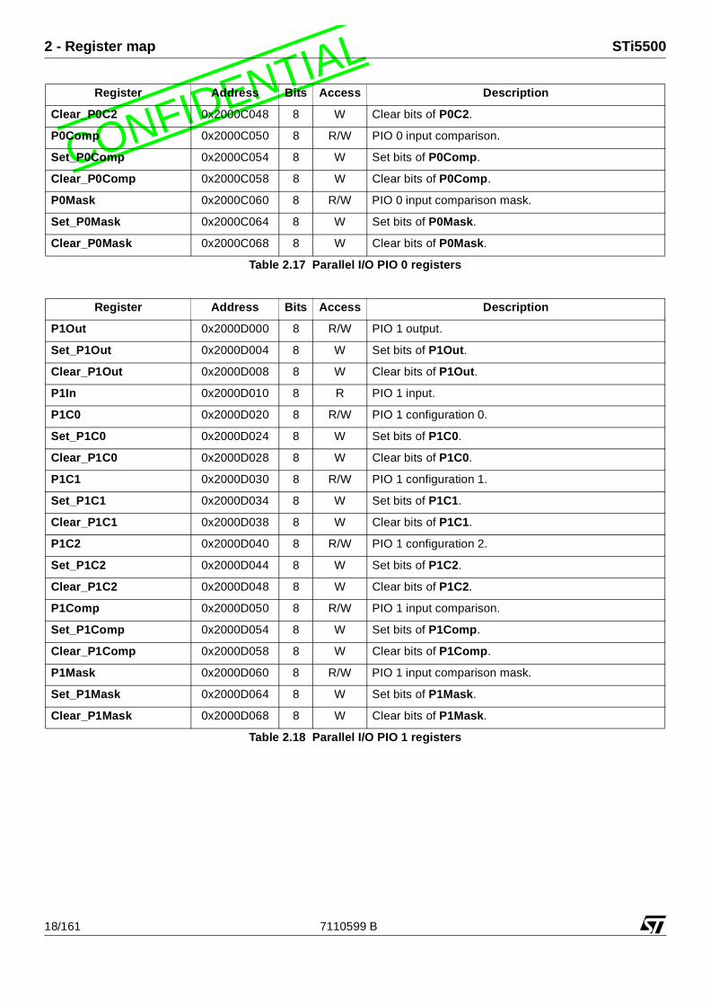
P0Out 0x2000C000 8 R/W PIO 0 output.
Set_P0Out 0x2000C004 8 W Set bits of P0Out.
Clear_P0Out 0x2000C008 8 W Clear bits of P0Out.
P0In 0x2000C010 8 R PIO 0 input.
P0C0 0x2000C020 8 R/W PIO 0 configuration 0.
Set_P0C0 0x2000C024 8 W Set bits of P0C0.
Clear_P0C0 0x2000C028 8 W Clear bits of P0C0.
P0C1 0x2000C030 8 R/W PIO 0 configuration 1.
Set_P0C1 0x2000C034 8 W Set bits of P0C1.
Clear_P0C1 0x2000C038 8 W Clear bits of P0C1.
P0C2 0x2000C040 8 R/W PIO 0 configuration 2.
Set_P0C2 0x2000C044 8 W Set bits of P0C2.
Table 2.17 Parallel I/O PIO 0 registers
Register Address Bits Access Description
Table 2.16 PWM/counter module registers
7110599 B 17/161
L2 - Register map STi5500
CONFIDENTIAClear_P0C2 0x2000C048 8 W Clear bits of P0C2.
P0Comp 0x2000C050 8 R/W PIO 0 input comparison.
Set_P0Comp 0x2000C054 8 W Set bits of P0Comp.
Clear_P0Comp 0x2000C058 8 W Clear bits of P0Comp.
P0Mask 0x2000C060 8 R/W PIO 0 input comparison mask.
Set_P0Mask 0x2000C064 8 W Set bits of P0Mask.
Clear_P0Mask 0x2000C068 8 W Clear bits of P0Mask.
Register Address Bits Access Description
P1Out 0x2000D000 8 R/W PIO 1 output.
Set_P1Out 0x2000D004 8 W Set bits of P1Out.
Clear_P1Out 0x2000D008 8 W Clear bits of P1Out.
P1In 0x2000D010 8 R PIO 1 input.
P1C0 0x2000D020 8 R/W PIO 1 configuration 0.
Set_P1C0 0x2000D024 8 W Set bits of P1C0.
Clear_P1C0 0x2000D028 8 W Clear bits of P1C0.
P1C1 0x2000D030 8 R/W PIO 1 configuration 1.
Set_P1C1 0x2000D034 8 W Set bits of P1C1.
Clear_P1C1 0x2000D038 8 W Clear bits of P1C1.
P1C2 0x2000D040 8 R/W PIO 1 configuration 2.
Set_P1C2 0x2000D044 8 W Set bits of P1C2.
Clear_P1C2 0x2000D048 8 W Clear bits of P1C2.
P1Comp 0x2000D050 8 R/W PIO 1 input comparison.
Set_P1Comp 0x2000D054 8 W Set bits of P1Comp.
Clear_P1Comp 0x2000D058 8 W Clear bits of P1Comp.
P1Mask 0x2000D060 8 R/W PIO 1 input comparison mask.
Set_P1Mask 0x2000D064 8 W Set bits of P1Mask.
Clear_P1Mask 0x2000D068 8 W Clear bits of P1Mask.
Table 2.18 Parallel I/O PIO 1 registers
Register Address Bits Access Description
Table 2.17 Parallel I/O PIO 0 registers
18/161 7110599 B

LSTi5500 2 - Register map
CONFIDENTIARegister Address Bits Access Description
P2Out 0x2000E000 8 R/W PIO 2 output.
Set_P2Out 0x2000E004 8 W Set bits of P2Out.
Clear_P2Out 0x2000E008 8 W Clear bits of P2Out.
P2In 0x2000E010 8 R PIO 2 input.
P2C0 0x2000E020 8 R/W PIO 2 configuration 0.
Set_P2C0 0x2000E024 8 W Set bits of P2C0.
Clear_P2C0 0x2000E028 8 W Clear bits of P2C0.
P2C1 0x2000E030 8 R/W PIO 2 configuration 1.
Set_P2C1 0x2000E034 8 W Set bits of P2C1.
Clear_P2C1 0x2000E038 8 W Clear bits of P2C1.
P2C2 0x2000E040 8 R/W PIO 2 configuration 2.
Set_P2C2 0x2000E044 8 W Set bits of P2C2.
Clear_P2C2 0x2000E048 8 W Clear bits of P2C2.
P2Comp 0x2000E050 8 R/W PIO 2 input comparison.
Set_P2Comp 0x2000E054 8 W Set bits of P2Comp.
Clear_P2Comp 0x2000E058 8 W Clear bits of P2Comp.
P2Mask 0x2000E060 8 R/W PIO 2 input comparison mask.
Set_P2Mask 0x2000E064 8 W Set bits of P2Mask.
Clear_P2Mask 0x2000E068 8 W Clear bits of P2Mask.
Table 2.19 Parallel I/O PIO 2 registers
Register Address Bits Access Description
P3Out 0x2000F000 8 R/W PIO 3 output.
Set_P3Out 0x2000F004 8 W Set bits of P3Out.
Clear_P3Out 0x2000F008 8 W Clear bits of P3Out.
P3In 0x2000F010 8 R PIO 3 input.
P3C0 0x2000F020 8 R/W PIO 3 configuration 0.
Set_P3C0 0x2000F024 8 W Set bits of P3C0.
Clear_P3C0 0x2000F028 8 W Clear bits of P3C0.
P3C1 0x2000F030 8 R/W PIO 3 configuration 1.
Set_P3C1 0x2000F034 8 W Set bits of P3C1.
Clear_P3C1 0x2000F038 8 W Clear bits of P3C1.
P3C2 0x2000F040 8 R/W PIO 3 configuration 2.
Set_P3C2 0x2000F044 8 W Set bits of P3C2.
Table 2.20 Parallel I/O PIO 3 registers
7110599 B 19/161

L2 - Register map STi5500
CONFIDENTIAClear_P3C2 0x2000F048 8 W Clear bits of P3C2.
P3Comp 0x2000F050 8 R/W PIO 3 input comparison.
Set_P3Comp 0x2000F054 8 W Set bits of P3Comp.
Clear_P3Comp 0x2000F058 8 W Clear bits of P3Comp.
P3Mask 0x2000F060 8 R/W PIO 3 input comparison mask.
Set_P3Mask 0x2000F064 8 W Set bits of P3Mask.
Clear_P3Mask 0x2000F068 8 W Clear bits of P3Mask.
Register Address Bits Access Description
P4Out 0x20010000 2 R/W PIO 4 output.
Set_P4Out 0x20010004 2 W Set bits of P4Out.
Clear_P4Out 0x20010008 2 W Clear bits of P4Out.
P4In 0x20010010 2 R PIO 4 input.
P4C0 0x20010020 2 R/W PIO 4 configuration 0.
Set_P4C0 0x20010024 2 W Set bits of P4C0.
Clear_P4C0 0x20010028 2 W Clear bits of P4C0.
P4C1 0x20010030 2 R/W PIO 4 configuration 1.
Set_P4C1 0x20010034 2 W Set bits of P4C1.
Clear_P4C1 0x20010038 2 W Clear bits of P4C1.
P4C2 0x20010040 2 R/W PIO 4 configuration 2.
Set_P4C2 0x20010044 2 W Set bits of P4C2.
Clear_P4C2 0x20010048 2 W Clear bits of P4C2.
P4Comp 0x20010050 2 R/W PIO 4 input comparison.
Set_P4Comp 0x20010054 2 W Set bits of P4Comp.
Clear_P4Comp 0x20010058 2 W Clear bits of P4Comp.
P4Mask 0x20010060 2 R/W PIO 4 input comparison mask.
Set_P4Mask 0x20010064 2 W Set bits of P4Mask.
Clear_P4Mask 0x20010068 2 W Clear bits of P4Mask.
Table 2.21 Parallel I/O PIO 4 registers
Register Address Bits Access Description
Table 2.20 Parallel I/O PIO 3 registers
20/161 7110599 B
LSTi5500 2 - Register map
CONFIDENTIARegister Address Bits Access Description
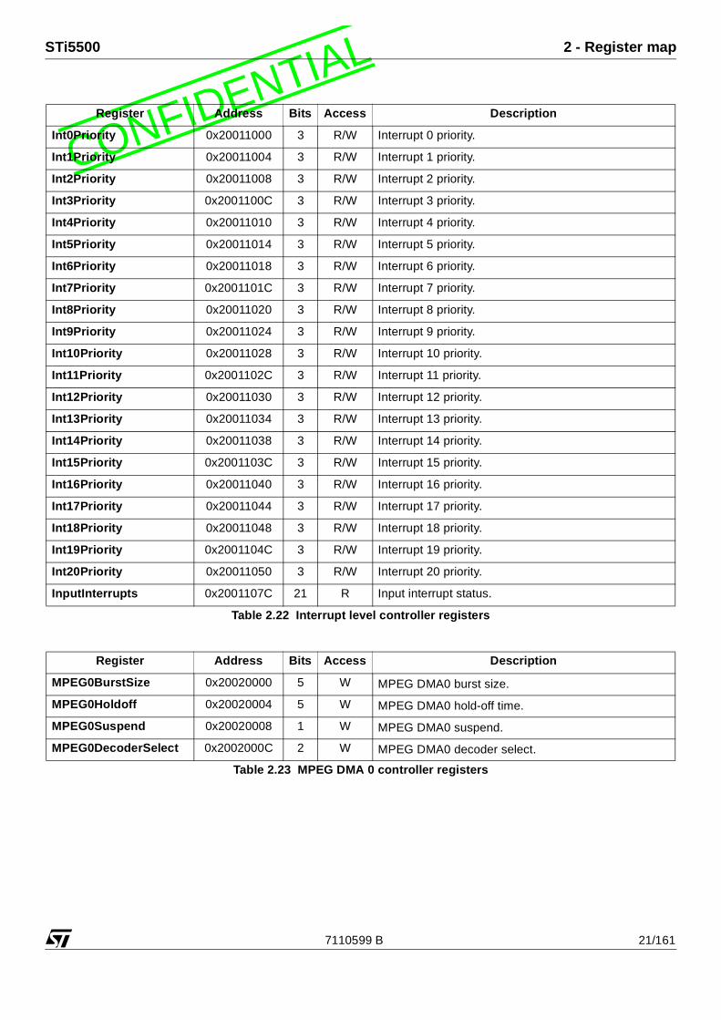
Int0Priority 0x20011000 3 R/W Interrupt 0 priority.
Int1Priority 0x20011004 3 R/W Interrupt 1 priority.
Int2Priority 0x20011008 3 R/W Interrupt 2 priority.
Int3Priority 0x2001100C 3 R/W Interrupt 3 priority.
Int4Priority 0x20011010 3 R/W Interrupt 4 priority.
Int5Priority 0x20011014 3 R/W Interrupt 5 priority.
Int6Priority 0x20011018 3 R/W Interrupt 6 priority.
Int7Priority 0x2001101C 3 R/W Interrupt 7 priority.
Int8Priority 0x20011020 3 R/W Interrupt 8 priority.
Int9Priority 0x20011024 3 R/W Interrupt 9 priority.
Int10Priority 0x20011028 3 R/W Interrupt 10 priority.
Int11Priority 0x2001102C 3 R/W Interrupt 11 priority.
Int12Priority 0x20011030 3 R/W Interrupt 12 priority.
Int13Priority 0x20011034 3 R/W Interrupt 13 priority.
Int14Priority 0x20011038 3 R/W Interrupt 14 priority.
Int15Priority 0x2001103C 3 R/W Interrupt 15 priority.
Int16Priority 0x20011040 3 R/W Interrupt 16 priority.
Int17Priority 0x20011044 3 R/W Interrupt 17 priority.
Int18Priority 0x20011048 3 R/W Interrupt 18 priority.
Int19Priority 0x2001104C 3 R/W Interrupt 19 priority.
Int20Priority 0x20011050 3 R/W Interrupt 20 priority.
InputInterrupts 0x2001107C 21 R Input interrupt status.
Table 2.22 Interrupt level controller registers
Register Address Bits Access Description
MPEG0BurstSize 0x20020000 5 W MPEG DMA0 burst size.
MPEG0Holdoff 0x20020004 5 W MPEG DMA0 hold-off time.
MPEG0Suspend 0x20020008 1 W MPEG DMA0 suspend.
MPEG0DecoderSelect 0x2002000C 2 W MPEG DMA0 decoder select.
Table 2.23 MPEG DMA 0 controller registers
7110599 B 21/161

L2 - Register map STi5500
CONFIDENTIARegister Address Bits Access Description
MPEG1BurstSize 0x20021000 5 W MPEG DMA1 burst size.
MPEG1Holdoff 0x20021004 5 W MPEG DMA1 hold-off time.
MPEG1Suspend 0x20021008 1 W MPEG DMA1 suspend.
MPEG1DecoderSelect 0x2002100C 2 W MPEG DMA1 decoder select.
Table 2.24 MPEG DMA 1 controller registers
Register Address Bits Access Description
MPEG2BurstSize 0x20022000 5 W MPEG DMA2 burst size.
MPEG2Holdoff 0x20022004 5 W MPEG DMA2 hold-off time.
MPEG2Suspend 0x20022008 1 W MPEG DMA2 suspend.
MPEG2DecoderSelect 0x2002200C 2 W MPEG DMA2 decoder select.
Table 2.25 MPEG DMA 2 controller registers
Register Address Bits Access Description
TtxtDmaAddress 0x20024000 32 R/W Teletext DMA address.
TtxtDmaCount 0x20024004 11 R/W Teletext DMA count.
TtxtOutDelay 0x20024008 9 R/W Teletext output delay.
TtxtMode 0x20024014 2 R/W Teletext mode.
TtxtIntStatus 0x20024018 3 R Teletext interrupt status.
TtxtIntEnable 0x2002401C 3 R/W Teletext interrupt enable.
TtxtAckOddEven 0x20024020 1 W Teletext acknowledge odd or even.
TtxAbort 0x20024024 1 W Teletext abort.
Table 2.26 Teletext interface registers
Register Address Bits Access Description
BMDMADestAddress 0x20026000 32 W Block move DMA destination address.
22/161 7110599 B

LSTi5500 3 - Asynchronous serial controller (ASC) registers
CONFIDENTIA3 Asynchronous serial controller (ASC) registers
ASCnBaudRate ASCn baud rate generator
Address: ASCnBaseAddress + 0x00Access: Read/writeReset state: 1
Description
The ASCnBaudRate register is the dual-function baud rate generator and reload value register. A read from this regis-ter returns the content of the 16-bit timer; writing to it updates the 16-bit reload register. If the Run bit of the control register is 1, then any value written in the ASCnBaudRate register is immediately copied tothe timer. However, if the Run bit is 0 when the register is written, then the timer will not be reloaded until the first CPUclock cycle after the Run bit is 1.The baud rate and the required reload value for a given baud rate can be determined by the following formulae:
where: RegisterVal represents the content of the ASCnBaudRate register, taken as an unsigned 16-bit integer,fCPU is the frequency of the CPU.
Table 3.1 lists commonly used baud rates with the required reload values and the approximate deviation errors for anexample baud rate with a CPU clock of 50 MHz. This does not imply availability of a 50 MHz device.
31 30 29 28 28 26 25 24 23 22 21 20 19 18 17 16 15 14 13 12 11 10 9 8 7 6 5 4 3 2 1 0
0x00 ReloadVal
Baud rateReload value
(exact)
Reload value
(integer)
Reload value
(hex)Approximate
deviation error
625 K 5 5 0005 0%
38.4 K 81.380 81 0051 0.1%
19.2 K 162.760 163 00A3 0.1%
9600 325.521 325 0145 0.2%
4800 651.042 651 028B 0.01%
2400 1302.083 1302 0516 0.01%
1200 2604.167 2604 0A2C 0.01%
600 5208.33 5208 1458 0.01%
300 10416.667 10417 28B1 0.01%
75 41666.667 41667 A2C3 0.01%
Table 3.1 Baud rates
BaudRate =16 x RegisterVal
RegisterVal =16 x BaudRate
fCPU
fCPU
7110599 B 23/161

L3 - Asynchronous serial controller (ASC) registers STi5500
CONFIDENTIAASCnControl ASCn control register
Address: ASCnBaseAddress + 0x0CAccess: Read/writeReset state: 0
Description
The ASCnControl register controls the operating mode of the UART ASCn and contains control bits for mode anderror check selection, and status flags for error identification. The format of the register is shown in the ASCn controlregister bit description table below.Programming the mode control field (Mode) to one of the reserved combinations may result in unpredictable behavior.Serial data transmission or reception is only possible when the baud rate generator run bit (Run) is set to 1. When theRun bit is set to 0, TxD will be 1. Setting the Run bit to 0 will immediately freeze the state of the transmitter andreceiver. This should only be done when the ASC is idle.Serial data transmission or reception is only possible when the baud rate generator Run bit is set to 1. A transmissionis started by writing to the transmit buffer register ASCnTxBuffer.
31 30 29 28 28 26 25 24 23 22 21 20 19 18 17 16 15 14 13 12 11 10 9 8 7 6 5 4 3 2 1 0
0x0C
ScE
nab
le
RxE
nab
le
Ru
n
Lo
op
Bac
k
Par
ityO
dd
StopBits
Mode
24/161 7110599 B

LSTi5500 3 - Asynchronous serial controller (ASC) registers
CONFIDENTIABit Bit field Function
2:0 Mode
ASC mode control:
Mode2:0 Mode000 RESERVED.001 8-bit data.010 RESERVED.011 7-bit data + parity.100 9-bit data.101 8-bit data + wake up bit.110 RESERVED.111 8-bit data + parity.
4:3 StopBits
Number of stop bits selection:
StopBits1:0 Number of stop bits00 0.5 stop bits.01 1 stop bits.10 1.5 stop bits.11 2 stop bits.
5 ParityOddParity selection:
0 Even parity (parity bit set on odd number of ‘1’s in data).1 Odd parity (parity bit set on even number of ‘1’s in data).
6 LoopBackLoopback mode enable bit:
0 Standard transmit/receive mode.1 Loopback mode enabled.
7 RunBaudrate generator run bit:
0 Baudrate generator disabled (ASC inactive).1 Baudrate generator enabled.
8 RxEnableReceiver enable bit:
0 Receiver disabled.1 Receiver enabled.
9 ScEnableSmartCard enable bit:
0 SmartCard mode disabled.1 SmartCard mode enabled.
7110599 B 25/161

L3 - Asynchronous serial controller (ASC) registers STi5500
CONFIDENTIAASCnIntEnable ASCn interrupt enable
Address: ASCnBaseAddress + 0x10Access: Read/writeReset state: 0
Description
31 30 29 28 28 26 25 24 23 22 21 20 19 18 17 16 15 14 13 12 11 10 9 8 7 6 5 4 3 2 1 0
0x10
RH
F
TOI
TN
E
OE
FE
PE
TB
E
TE
RB
E
Bit Bit field Function
0 RBE RxBufFullIEReceiver buffer full interrupt enable:
0 Receiver buffer full interrupt disable.1 Receiver buffer full interrupt enable.
1 TE TxEmptyIETransmitter empty interrupt enable:
0 Transmitter empty interrupt disable.1 Transmitter empty interrupt enable.
2 TBE TxBufEmptyIETransmitter buffer empty interrupt enable:+
0 Transmitter buffer empty interrupt disable.1 Transmitter buffer empty interrupt enable.
2 THE TxHalfEmptyIETransmitter buffer half empty interrupt enable:
0 Transmitter buffer half empty interrupt disable.1 Transmitter buffer half empty interrupt enable.
3 PE ParityErrorIEParity error interrupt enable:
0 Parity error interrupt disable.1 Parity error interrupt enable.
4 FE FrameErrorIEFraming error interrupt enable:
0 Framing error interrupt disable.1 Framing error interrupt enable.
5 OE OverrunErrorIEOverrun error interrupt enable:
0 Overrun error interrupt disable.1 Overrun error interrupt enable.
6 TNE TimeoutNotEmptyIETime-out when not empty interrupt enable:
0 Time-out when input FIFO or buffer not empty interrupt disable.1 Time-out when input FIFO or buffer not empty interrupt enable.
7 TOI TimeoutIdleIETime-out when the receiver FIFO is empty interrupt enable:
0 Time-out when the input FIFO or buffer is empty interrupt disable.1 Time-out when the input FIFO or buffer is empty interrupt enable.
8 RHF RxHalfFullIEReceiver FIFO is half full interrupt enable:
0 Receiver FIFO is half full interrupt disable.1 Receiver FIFO is half full interrupt enable.
26/161 7110599 B

LSTi5500 3 - Asynchronous serial controller (ASC) registers
CONFIDENTIAASCnRxBuffer ASCn Rx buffer
Address: ASCnBaseAddress + 0x08Access: Read onlyReset state: 0
Description
Serial data reception is only possible when the baud rate generator Run bit in the ASCnControl register is set to 1.
31 30 29 28 28 26 25 24 23 22 21 20 19 18 17 16 15 14 13 12 11 10 9 8 7 6 5 4 3 2 1 0
0x08 RD
ASCnRxBufferASCnBaseAddress + #08Read only
Bit Bit field Function
0 RD0 Receive buffer data D0.
1 RD1 Receive buffer data D1.
2 RD2 Receive buffer data D2.
3 RD3 Receive buffer data D3.
4 RD4 Receive buffer data D4.
5 RD5 Receive buffer data D5.
6 RD6 Receive buffer data D6.
7 RD7/Parity Receive buffer data D7, or parity bit - depending on the operating mode (the setting of theMode bit of the ASCControl register).
8RD8/Parity/Wake/X
Receive buffer data D8, or parity bit, or wake-up bit - depending on the operating mode (thesetting of the Mode field of the ASCControl register)
If the Mode field selects an 8-bit frame then this bit is undefined. Software should ignorethis bit when reading 8-bit frames
15:9 Reserved. Read back 0.
7110599 B 27/161

L3 - Asynchronous serial controller (ASC) registers STi5500
CONFIDENTIAASCnStatus ASCn interrupt status
Address: ASCnBaseAddress + 0x14Access: Read onlyReset state: 3 (i.e. Rx buffer full and Tx buffer empty)
Description
31 30 29 28 28 26 25 24 23 22 21 20 19 18 17 16 15 14 13 12 11 10 9 8 7 6 5 4 3 2 1 0
0x14 TF
RH
F
TOI
TN
E
OE
FE
PE
TB
E
TE
RB
F
Bit Bit field Function
0 RBF RxBufFullReceiver buffer full flag:
0 Receiver buffer is not full.1 Receiver buffer is full.
1 TE TxEmptyTransmitter empty flag:
0 Transmitter is not empty.1 Transmitter is empty.
2 TBE TxBufEmptyTransmitter buffer empty flag:
0 Transmitter buffer not empty.1 Transmitter buffer empty.
2 THE TxHalfEmpty
Transmitter FIFO at least half empty flag or buffer empty:
0 The FIFOs are enabled and the transmitter FIFO is more than half full or theFIFOs are disabled and the transmit buffer is not empty.
1 The FIFOs are enabled and the transmitter FIFO is at least half empty or theFIFOs are disabled and the transmit buffer is empty.
3 PE ParityErrorInput parity error flag:
0 No parity error.1 Parity error.
4 FE FrameErrorInput frame error flag, i.e.stop bits not found:
0 No framing error.1 Framing error.
5 OE OverrunErrorOverrun error flag:
0 No overrun error.1 Overrun error, i.e. data received when the input buffer is full.
6 TNE TimeoutNotEmptyTime-out when the receiver FIFO or buffer is not empty:
0 No time-out or the receiver FIFO or buffer is empty.1 Time-out when the receiver FIFO or buffer is not empty.
7 TOI TimeoutIdleTime-out when the receiver FIFO or buffer is empty:
0 No time-out or the receiver FIFO or buffer is not empty.1 Time-out when the receiver FIFO or buffer is empty.
8 RHF RxHalfFullReceiver FIFO is half full:
0 The receiver FIFO contains less than 8 characters.1 The receiver FIFO contains at least 8 characters.
9 TF TxFull
Transmitter FIFO or buffer is full:
0 The FIFOs are enabled and the transmitter FIFO is empty or contains lessthan 16 characters or the FIFOs are disabled and the transmit buffer is empty.
1 The FIFOs are enabled and the transmitter FIFO contains 16 characters orthe FIFOs are disabled and the transmit buffer is full.
28/161 7110599 B

LSTi5500 3 - Asynchronous serial controller (ASC) registers
CONFIDENTIAASCnTimeout ASCn time out
Address: ASCnBaseAddress + 0x1CAccess: Read/writeReset state: 0
DescriptionThe time-out period in baud rate ticks. The ASC contains an 8-bit time-out counter, which reloads from ASCnTimeoutwhenever one or more of the following is true:
• ASCnRxBuffer is read;• the ASC is in the middle of receiving a character;• ASCnTimeout is written to.
If none of these conditions hold the counter decrements towards 0 at every baud rate tick.The TimeoutNotEmpty bit of the ASCnStatus register is 1 when the input FIFO is not empty and the time-out counteris zero.The TimeoutIdle bit of the ASCnStatus register is 1 when the input FIFO is empty and the time-out counter iszero. When the software has emptied the input FIFO, the time-out counter will reset and start decrementing. If no more char-acters arrive, when the counter reaches zero the TimeoutIdle bit of the ASCnStatus register will be set.
31 30 29 28 28 26 25 24 23 22 21 20 19 18 17 16 15 14 13 12 11 10 9 8 7 6 5 4 3 2 1 0
0x1C Timeout
7110599 B 29/161

L3 - Asynchronous serial controller (ASC) registers STi5500
CONFIDENTIAASCnTxBuffer ASCn Tx buffer
Address: ASCnBaseAddress + 0x04Access: Write onlyReset state: 0
DescriptionA transmission is started by writing to the transmit buffer register ASCnTxBuffer. Serial data transmission is only pos-sible when the baud rate generator Run bit in the ASCnControl register is set to 1. Data transmission is double-buff-ered, so a new character may be written to the transmit buffer register before the transmission of the previouscharacter is complete. This allows characters to be sent back-to-back without gaps.
31 30 29 28 28 26 25 24 23 22 21 20 19 18 17 16 15 14 13 12 11 10 9 8 7 6 5 4 3 2 1 0
0x04 TD
Bit Bit field Function
0 TD0 Transmit buffer data D0.
1 TD1 Transmit buffer data D1.
2 TD2 Transmit buffer data D2.
3 TD3 Transmit buffer data D3.
4 TD4 Transmit buffer data D4.
5 TD5 Transmit buffer data D5.
6 TD6 Transmit buffer data D6.
7 TD7/Parity Transmit buffer data D7, or parity bit - depending on the operating mode (the setting of theMode field of the ASCControl register).
8TD8/Parity
/Wake/0
Transmit buffer data D8, or parity bit, or wake-up bit or undefined - depending on theoperating mode (the setting of the Mode field of the ASCControl register).
If the Mode field selects an 8-bit frame then this bit should be written as 0.
15:9 Reserved. Write 0.
30/161 7110599 B
LSTi5500 4 - Audio MPEG (AUD) registers
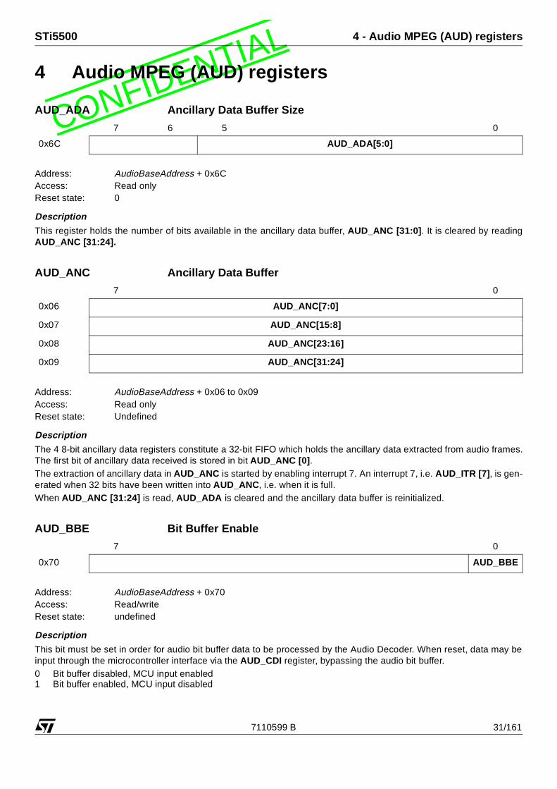
CONFIDENTIA4 Audio MPEG (AUD) registers
AUD_ADA Ancillary Data Buffer Size
Address: AudioBaseAddress + 0x6CAccess: Read onlyReset state: 0
Description
This register holds the number of bits available in the ancillary data buffer, AUD_ANC [31:0]. It is cleared by readingAUD_ANC [31:24].
AUD_ANC Ancillary Data Buffer
Address: AudioBaseAddress + 0x06 to 0x09Access: Read onlyReset state: Undefined
Description
The 4 8-bit ancillary data registers constitute a 32-bit FIFO which holds the ancillary data extracted from audio frames.The first bit of ancillary data received is stored in bit AUD_ANC [0].The extraction of ancillary data in AUD_ANC is started by enabling interrupt 7. An interrupt 7, i.e. AUD_ITR [7], is gen-erated when 32 bits have been written into AUD_ANC, i.e. when it is full.When AUD_ANC [31:24] is read, AUD_ADA is cleared and the ancillary data buffer is reinitialized.
AUD_BBE Bit Buffer Enable
Address: AudioBaseAddress + 0x70Access: Read/writeReset state: undefined
Description
This bit must be set in order for audio bit buffer data to be processed by the Audio Decoder. When reset, data may beinput through the microcontroller interface via the AUD_CDI register, bypassing the audio bit buffer.0 Bit buffer disabled, MCU input enabled1 Bit buffer enabled, MCU input disabled
7 6 5 0
0x6C AUD_ADA[5:0]
7 0
0x06 AUD_ANC[7:0]
0x07 AUD_ANC[15:8]
0x08 AUD_ANC[23:16]
0x09 AUD_ANC[31:24]
7 0
0x70 AUD_BBE
7110599 B 31/161

L4 - Audio MPEG (AUD) registers STi5500
CONFIDENTIAAUD_CDI Compressed Data Input
Address: AudioBaseAddress + 0x18Access: Write onlyReset state: Undefined
Description
When AUD_BBE is reset, audio compressed data may be input via the microcontroller by writing the compressed datato this register. Note that as audio data enters the audio decoder directly, the system parser and bit buffer arebypassed. Thus, only elementary or PCM audio data may be entered, and these modes must be correctly programmedin the AUD_ISS register.
AUD_CRC CRC Error Concealment Mode
Address: AudioBaseAddress + 0x2AAccess: Read/WriteReset state: Undefined
DescriptionThis register defines the action which will be taken upon detection of a CRC error in an input frame.00 Disable CRC detection and error concealment01 Mute on detection of CRC error10 Illegal11 Skip invalid frame
AUD_DEM De-Emphasis Mode
Address: AudioBaseAddress + 0x46Access: Read onlyReset state: Undefined
Description
This register is set with the value of the emphasis field of the frame currently being decoded. If enabled, an interrupt10, i.e. AUD_ITR [10], is generated on a change in the value. The register is updated and the interrupt generatedwhen the corresponding frame is at the PCM output stage.00 None01 50/15 µs10 Reserved.11 ITU-T J.17
7 0
0x18 AUD_CDI[7:0]
7 1 0
0x2A AUD_CRC[1:0]
7 1 0
0x46 AUD_DEM[1:0]
32/161 7110599 B
LSTi5500 4 - Audio MPEG (AUD) registers
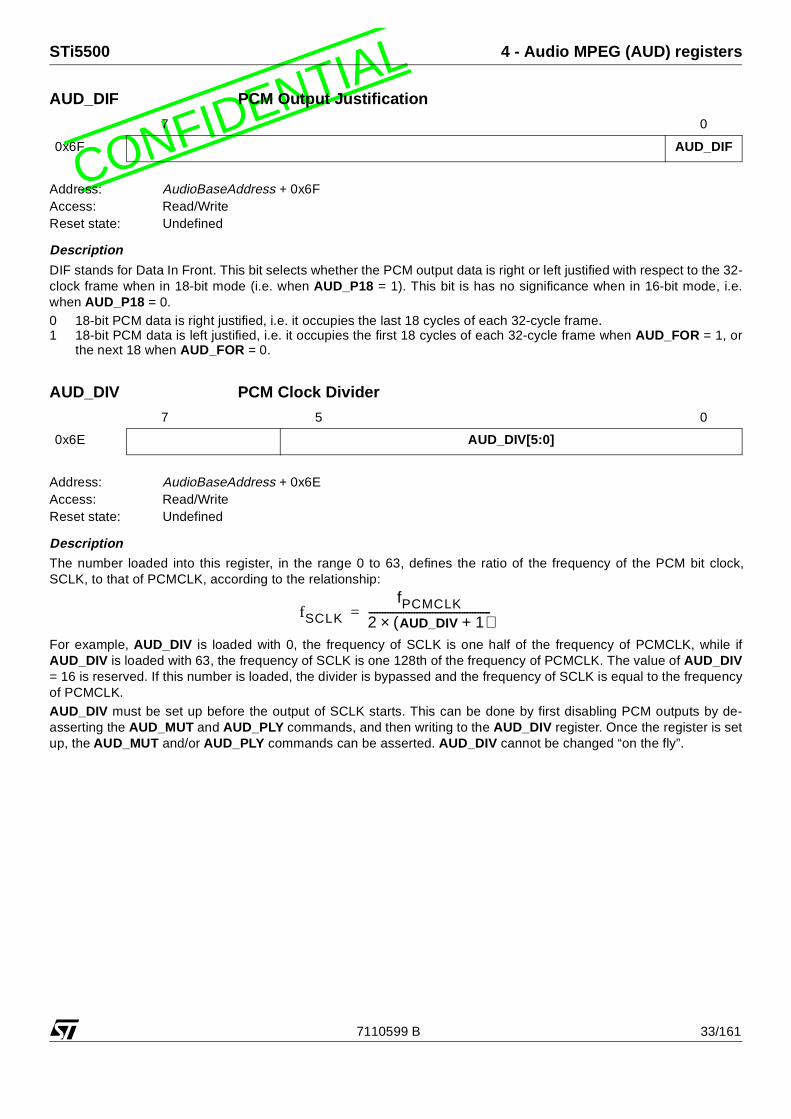
CONFIDENTIAAUD_DIF PCM Output Justification
Address: AudioBaseAddress + 0x6FAccess: Read/WriteReset state: Undefined
Description
DIF stands for Data In Front. This bit selects whether the PCM output data is right or left justified with respect to the 32-clock frame when in 18-bit mode (i.e. when AUD_P18 = 1). This bit is has no significance when in 16-bit mode, i.e.when AUD_P18 = 0.0 18-bit PCM data is right justified, i.e. it occupies the last 18 cycles of each 32-cycle frame.1 18-bit PCM data is left justified, i.e. it occupies the first 18 cycles of each 32-cycle frame when AUD_FOR = 1, or
the next 18 when AUD_FOR = 0.
AUD_DIV PCM Clock Divider
Address: AudioBaseAddress + 0x6EAccess: Read/WriteReset state: Undefined
DescriptionThe number loaded into this register, in the range 0 to 63, defines the ratio of the frequency of the PCM bit clock,SCLK, to that of PCMCLK, according to the relationship:
For example, AUD_DIV is loaded with 0, the frequency of SCLK is one half of the frequency of PCMCLK, while ifAUD_DIV is loaded with 63, the frequency of SCLK is one 128th of the frequency of PCMCLK. The value of AUD_DIV= 16 is reserved. If this number is loaded, the divider is bypassed and the frequency of SCLK is equal to the frequencyof PCMCLK.AUD_DIV must be set up before the output of SCLK starts. This can be done by first disabling PCM outputs by de-asserting the AUD_MUT and AUD_PLY commands, and then writing to the AUD_DIV register. Once the register is setup, the AUD_MUT and/or AUD_PLY commands can be asserted. AUD_DIV cannot be changed “on the fly”.
7 0
0x6F AUD_DIF
7 5 0
0x6E AUD_DIV[5:0]
fSCLK
fPCMCLK
2 AUD_DIV 1+( )×----------------------------------------------=
7110599 B 33/161

L4 - Audio MPEG (AUD) registers STi5500
CONFIDENTIAAUD_ESC Elementary Stream Clock Reference
Address: AudioBaseAddress + 0x0A to 0x0FAccess: Read onlyReset state: undefined
DescriptionThe register contains the value of the last elementary stream clock reference (ESCR) which was detected in the audiobitstream. When a new ESCR is detected an interruption is signalled. See register description AUD_INT, AUD_IMS.AUD_ESC[33] indicates the presence of the extension field AUD_ESCX[7:0] for 27 MHz system clocks.
AUD_EXT Decoding Mode Extension
Address: AudioBaseAddress + 0x1FAccess: Read/writeReset state: undefined
DescriptionThis register enables “dual-mode” decoding and an improved mute.00 Normal decoding01 Decode dual-mode bitstream, where only right channel is decoded and is output on both output channels10 Decode dual-mode bitstream, where only left channel is decoded and is output on both output channels11 Perform “smooth” mute by clearing 32 input samples.
AUD_FFL Free-Format Frame Length
Address: AudioBaseAddress + 0x14 to 0x15Access: Read/writeReset state: undefined
DescriptionWhen free-format decoding is used (bitrate_index = 0), the frame length, if known, can be loaded into this register, inunits of bits. (In free-format, the frame length cannot be determined from bitstream parameters).
7 0
0x0A AUD_ESC[7:0]
0x0B AUD_ESC[15:8]
0x0C AUD_ESC[23:16]
0x0D AUD_ESC[31:24]
0x0E AUD_ESC[33:32]
0x0F AUD_ESCX[7:0]
7 1 0
0x1F AUD_EXT[1:0]
7 0
0x14 AUD_FFL[7:0]
0x15 AUD_FFL[15:8]
34/161 7110599 B

LSTi5500 4 - Audio MPEG (AUD) registers
CONFIDENTIAThe length loaded into AUD_FFL is used in the internal synchronization algorithm. If the frame length is not known,AUD_FFL must be loaded with zero.
AUD_FOR PCM Output Format
Address: AudioBaseAddress + 0x19Access: Read/writeReset state: undefined
DescriptionThis bit is used to select the I2S-compatible PCM output format when in 18-bit left-justified mode (i.e. when AUD_P18= 1 and AUD_DIF = 1). In this mode the most-significant bit of the PCM data is output one cycle later than the changeof LRCK. AUD_FOR has no significance when AUD_P18 =0.0 I2S-compatible PCM output1 Standard format (most-significant bit of data coincident with AOLRCK)
AUD_HDR Frame Header
Address: AudioBaseAddress + 0x5E to 0x61Access: Read onlyReset state: undefined
Description
This 32-bit register contains the header of the frame currently being decoded.This register is updated after interrupt 1 is enabled. An interrupt 1 is generated, i.e. AUD_ITR[1], when a valid headerhas been received. The contents are retained until AUD_HDR[31:24] is read.
AUD_IDE Audio Stream ID Enable
Address: AudioBaseAddress + 0x24Access: Read/writeReset state: undefined
Description
If this bit is reset, then the contents of AUD_SID are ignored. If it is set, then the register AUD_SID is taken intoaccount. As they have opposite meanings, This bit and bit PES_CF1.IAI must always be forced to opposite values atthe “same time” (beginning with PES_CF1.IAI).
7 0
0x19 AUD_FOR
7 0
0x5E AUD_HDR[7:0]
0x5F AUD_HDR[15:8]
0x60 AUD_HDR[23:16]
0x61 AUD_HDR[31:24]
7 0
0x24 AUD_IDE
7110599 B 35/161

L4 - Audio MPEG (AUD) registers STi5500
CONFIDENTIA0 Ignore AUD_SID1 Use AUD_SID
AUD_IFT Input FIFO Threshold
Address: AudioBaseAddress + 0x52Access: Read/writeReset state: undefined
Description
This value loaded into this register defines the input FIFO level at which an interrupt 12 can be generated, i.e.AUD_ITR[12]. The level is defined as a byte address, in the range 0 to 255. An interrupt can be generated each timethe FIFO level is equal to AUD_IFT, regardless of whether it was approached from above or below. In addition, an inter-rupt 13, i.e AUD_ITR[13], is generated whenever the FIFO is full.Those interrupts AUD_ITR[13:12] are useful only when AUD_BBE is reset (i.e. Audio Bit Buffer disabled and datainput directly into audio decoder through AUD_CDI register followed by this input FIFO. Note that AUDREQ refers tothe input of data into the Bit Buffer (AUD_BBE is set). Thus controlling the direct input of audio data without Bit-Buffer,using AUD_ITR[13:12] is very constrained.
AUD_IMS Audio Interrupt Extension Mask
Address: AudioBaseAddress + 0x5CAccess: Read/writeReset state: undefined
Description
Interrupt status bits indicating new value for ESCR field received in MPEG-2 PES streams.Setting AUD_IMS[0] must always be tied low. Setting AUD_IMS[1] enables ESCR interrupt.
AUD_ISS Input Stream Selection
Address: AudioBaseAddress + 0x36Access: Read/writeReset state: undefined
DescriptionThis register defines the type of input bitstream expected by the audio decoder.000 MPEG audio elementary stream001 MPEG-1 packet stream010 reserved011 PCM data. In this mode, the audio decoder is bypassed and data is sent directly to the audio DAC interface. This
bit must be set in CD-DA mode.
7 0
0x52 AUD_IFT[7:0]
7 1 0
0x5C AUD_IMS[1:0]
7 2 0
0x36 AUD_ISS[2:0]
36/161 7110599 B

LSTi5500 4 - Audio MPEG (AUD) registers
CONFIDENTIA100 MPEG-2 PES Streams101 Automatic detection MPEG-1/MPEG-2 packet streams
AUD_ITM Interrupt Mask Register
Address: AudioBaseAddress + 0x1C to 0x1DAccess: Read/writeReset state: 0. Also cleared on restart.
Description
A one in any bit position of this register will enable the corresponding bit of the AUD_ITR register.In addition, setting certain bits of this register have additional actions, as specified below:Setting AUD_ITM[7] enables the reading of ancillary data into AUD_ANC.Setting AUD_ITM[2] enables the updating of the AUD_PTS register.Setting AUD_ITM[1] enables the updating of the AUD_HDR register.Setting AUD_ITM[0] enables the updating of the AUD_SYS register.
AUD_ITR Interrupt Status Request Register
Address: AudioBaseAddress + 0x1A to 0x1BAccess: Read onlyReset state: 0. Also cleared on restart.
DescriptionAn interrupt is signalled whenever one of the bits of AUD_ITR becomes set. This can only occur if the correspondingbit is set in the AUD_ITM register. The AUD_ITR register is cleared on reset (assertion of RESET pin or setting ofAUD_RES register), or restart (setting the AUD_RST register). Also the most significant byte, and bit 5 of the least sig-nificant byte of AUD_ITR can be independently cleared by reading. Bits 0-2 and 7 are cleared by a different method, asindicated in the notes in the table below.
7 6 0
0x1C AUD_ITM[7:0]
0x1D AUD_ITM[14:8]
7 6 0
0x1A AUD_ITR[7:0]
0x1B AUD_ITR[14:8]
Bit Condition Signalled Note
14 First bit of new frame at PCM output
13 Input FIFO full
12 Input FIFO level = FIFO_THRES
11 not used
10 De-emphasis changed
9 Sampling frequency changed
8 PCM output buffer underflow
7 Ancillary data register fullAUD_ANC[31:24] must be read in order to clear bit AUD_ITR[7] andto reinitialize the ancillary data buffer.
7110599 B 37/161

L4 - Audio MPEG (AUD) registers STi5500
CONFIDENTIA
AUD_ITS Audio Interrupt Extension
Address: AudioBaseAddress + 0x5BAccess: Read/writeReset state: undefined
DescriptionInterrupt status bits indicating new values for ESCR and DTS fields received in MPEG-2 PES streams.
AUD_LCA Left Channel Attenuation
Address: AudioBaseAddress + 0x1EAccess: Read/writeReset state: undefined
Description
This register defines the left channel attenuation in steps of 2dB. The minimum attenuation is 0 dB, the maximum is 2 x63 = 126 dB.
AUD_LCK Sync Words Until Lock
Address: AudioBaseAddress + 0x28Access: Read/writeReset state: undefined
6 not used
5 CRC error detected
4 not used
3 not used
2 Valid PTS registeredAUD_PTS[32] must be read in order to clear bit AUD_ITR[2] and toreinitialize the AUD_PTS register.
1 Valid header registeredAUD_HDR[31:24] must be read in order to clear bit AUD_ITR[1] andto reinitialize the AUD_HDR register.
0 Change in synchronization statusAUD_SYS must be read in order to clear bit AUD_ITR[0] and toreinitialize the AUD_SYS register.
7 1 0
0x5B AUD_ITS[1:0]
7 5 0
0x1E AUD_LCA[5:0]
7 1 0
0x28 AUD_LCK[1:0]
Bit Condition Signalled Note
38/161 7110599 B

LSTi5500 4 - Audio MPEG (AUD) registers
CONFIDENTIADescriptionThis register defines how many valid synchronization words after the initial one must be found before locking audioframe synchronization.When AUD_SYE is set to its default value, the audio decoder assumes that AUD_LCK is set to the value 3. Synchro-nization error concealment is still enabled when AUD_LCK has the value zero.
AUD_LRP LRCK Polarity
Address: AudioBaseAddress + 0x11Access: Read/writeReset state: 0 after assertion of RESET pin only
Description
This bit is used to define the polarity of the output signal LRCK.0 Left channel when LRCK = 11 Left channel when LRCK = 0
AUD_MUT Mute
Address: AudioBaseAddress + 0x30Access: Read/writeReset state: 0 after assertion of RESET pin only
Description
See audio processor description for more details.
AUD_ORD PCM Output Bit Order
Address: AudioBaseAddress + 0x38Access: Read/writeReset state: undefined
DescriptionThis bit determines the order of PCM data output when in 16-bit mode (i.e. when AUD_P18 = 0). It has no significancewhen AUD_P18 = 1, when data is always output most-significant bit first.0 Most-significant bit output first1 Least-significant bit output first
7 0
0x11 AUD_LRP
7 0
0x30 AUD_MUT
7 0
0x38 AUD_ORD
7110599 B 39/161

L4 - Audio MPEG (AUD) registers STi5500
CONFIDENTIAAUD_P18 PCM Output Precision
Address: AudioBaseAddress + 0x16Access: Read/writeReset state: undefined
Description
This bit defines the PCM output precision.0 16-bit PCM data output1 18-bit PCM data output
AUD_PLY Play
Address: AudioBaseAddress + 0x2EAccess: Read/writeReset state: 0 after assertion of RESET pin only
DescriptionSee audio processor section for more details.
AUD_PTS Presentation Time Stamp
Address: AudioBaseAddress + 0x62 to 0x66Access: Read onlyReset state: undefined
Description
This 33-bit register contains the PTS associated with the frame currently being decoded.This register is updated after interrupt 2 is enabled. An interrupt 2 is generated, i.e. AUD_ITR[2], when a valid PTS hasbeen received. The contents are retained until AUD_PTS[32] is read.
7 0
0x16 AUD_P18
7 0
0x2E AUD_PLY
7 0
0x62 AUD_PTS[7:0]
0x63 AUD_PTS[15:8]
0x64 AUD_PTS[23:16]
0x65 AUD_PTS[31:24]
0x66 AUD_PTS[32]
40/161 7110599 B

LSTi5500 4 - Audio MPEG (AUD) registers
CONFIDENTIAAUD_RCA Right Channel Attenuation
Address: AudioBaseAddress + 0x20Access: Read/writeReset state: undefined
Description
This register defines the right channel attenuation in steps of 2 dB. The minimum attenuation is 0 dB, the maximum is2 x 63 = 126 dB.
AUD_RES Audio Decoder Software Reset
Address: AudioBaseAddress + 0x40Access: Read/writeReset state: 0 (command)
DescriptionWriting a 0 or 1 to this bit has an equivalent function to audio only hardware reset, except that the following registersare not cleared:
• AUD_SCP• AUD_MUT• AUD_PLY
This bit is reset automatically after being set.
AUD_RST Restart
Address: AudioBaseAddress + 0x42Access: Read/writeReset state: (command)
Description
When this bit is set, all data buffers are flushed, and then the AUD_RST bit is automatically reset. In addition theAUD_ITR, AUD_ITM, AUD_IMS and AUD_IMT registers are cleared.
AUD_SCM Sync Confirmation Mode
Address: AudioBaseAddress + 0x25Access: Read/write
7 5 0
0x20 AUD_RCA[5:0]
7 0
0x40 AUD_RES
7 0
0x42 AUD_RST
7 0
0x25 AUD_SCM
7110599 B 41/161

L4 - Audio MPEG (AUD) registers STi5500
CONFIDENTIAReset state: undefined
DescriptionThis bit selects one of two options in the packet synchronization algorithm.0 After the first valid packet start code and stream ID are found, the packet length is used to locate the next start
code and stream ID before synchronization is confirmed and audio decoding starts.1 Synchronization is confirmed when the first valid packet start code and stream ID are found.
AUD_SCP SCLK Polarity
Address: AudioBaseAddress + 0x53Access: Read/writeReset state: 0 after assertion of RESET pin only
Description
This bit defines the polarity of the PCM bit clock output BCK.0 The LRCK and PCMDATA outputs change on the falling edge of SCLK. The external DAC will sample LRCLK and
PCMDATA on the rising edge of SCLK.1 The LRCK and PCMDATA outputs change on the rising edge of SCLK. The external DAC will sample LRCK and
PCMDATA on the falling edge of SCLK.
AUD_SEM Sync Error Concealment Mode
Address: AudioBaseAddress + 0x2CAccess: Read/writeReset state: undefined
DescriptionThis register defines the action which will be taken upon detection of a synchronization error.00 Ignore error01 Mute on detection of synchronization error10 Invalid.11 Skip invalid frame
AUD_SFR Sampling Frequency
Address: AudioBaseAddress + 0x44Access: Read onlyReset state: ’00’
7 0
0x53 AUD_SCP
7 1 0
0x2C AUD_SEM[1:0]
7 1 0
0x44 AUD_SFR[1:0]
42/161 7110599 B

LSTi5500 4 - Audio MPEG (AUD) registers
CONFIDENTIADescriptionThis register is loaded with the sampling frequency code extracted from the bit stream. The register is updated syn-chronously with the first sample out on the PCM data. If enabled, an interrupt 9 is generated, i.e. AUD_ITR[9], at thistime if the sampling frequency value has changed.00 44.1 kHz01 48 kHz10 32 kHz11 reserved
AUD_SID Audio Stream ID
Address: AudioBaseAddress + 0x22Access: Read/writeReset state: undefined
DescriptionThe value stored in this register is only taken into account if AUD_IDE is set. This register specifies the number(between 0 and 31) of the audio stream which is to be decoded. The stream number is defined in the field stream_id ofthe packet header. All other packets will be discarded. If AUD_IDE is reset, then all audio packets are decoded.Note that these bits are duplicated in register PES_CF1.AUD_ID[4:0] and should be set simultaneously.
AUD_SKP Skip Next Frame
Address: AudioBaseAddress + 0x32Access: Read/writeReset state: 0 (command)
Description
When this bit is set, the next audio frame is skipped, and then the AUD_SKP bit is automatically reset.
AUD_SYE Sync Word Extension
Address: AudioBaseAddress + 0x27Access: Read/writeReset state: undefined
7 4 0
0x22 AUD_SID[4:0]
7 0
0x32 AUD_SKP
7 0
0x27 AUD_SYE[7:0]
7110599 B 43/161

L4 - Audio MPEG (AUD) registers STi5500
CONFIDENTIADescriptionThis register defines an extension to the frame synchronization word which can be used to increase the reliability ofsynchronization when the layer number, bit rate or sampling frequency are known. The three fields are defined in thefollowing tables. Programming of this register is mandatory.
Examples:1 Layer II, 48 kHz sampling frequency, variable bit rate: AUD_SYE = 1011110122 Parameters unknown: AUD_SYE = 001111112
AUD_SYN Packet Sync Mode
Address: AudioBaseAddress + 0x23Access: Read/write
Bits 7,6 Mode
11 Layer I
10 Layer II
00 This field not used
Bits 5-2 Layer I Layer II
0000 free format free format
0001 32 kbit/s 32 kbit/s
0010 64 kbits 48 kbit/s
0011 96 kbit/s 56 kbit/s
0100 128 kbit/s 64 kbit/s
0101 160 kbit/s 80 kbit/s
0110 192 kbit/s 96 kbit/s
0111 224 kbit/s 112 kbit/s
1000 256 kbit/s 128 kbit/s
1001 288 kbit/s 160 kbit/s
1010 320 kbit/s 192 kbit/s
1011 352 kbit/s 224 kbit/s
1100 384 kbit/s 256 kbit/s
1101 416 kbit/s 320 kbit/s
1110 448 kbit/s 384 kbit/s
1111 This field not used This field not used
Bits 1,0 Mode
00 44.1 kHz
01 48 kHz
10 32 kHz
11 This field not used
7 1 0
0x23 AUD_SYN[1:0]
44/161 7110599 B

LSTi5500 4 - Audio MPEG (AUD) registers
CONFIDENTIAReset state: undefined
DescriptionThis register defines the packet synchronization mode.00 Synchronize only on 24-bit packet_start_code_prefix. (Multiplexed audio/video bitstream).01 Synchronize both on 24-bit packet_start_code_prefix and first 3 bits of stream_id. (Multiplexed audio bitstream).10 Synchronize both on 24-bit packet_start_code_prefix and all 8 bits of stream_id. (Audio bitstream with unique id).
AUD_SYS Synchronization Status
Address: AudioBaseAddress + 0x26Access: Read onlyReset state: undefined
Description
This register is loaded with the synchronization status on every synchronization cycle. This status values are:00 Unlocked 01 Attempting to recover lost synchronization11 LockedIf the status changes an interrupt 0 is generated, i.e. AUD_ITR[2]. The status must then be read and the interrupt
cleared by reading AUD_SYS.
AUD_VER Revision
Address: AudioBaseAddress + 0x2DAccess: Read onlyReset state: static
Description
This register holds the chip version number "x.y" where x is represented by bits 6-4 and y by bits 3-0. Bit 7 is always 1.
7 1 0
0x26 AUD_SYS[1:0]
7 1 0
0x2D 1AUD_REV[6:0]
7110599 B 45/161

L5 - Block move DMA (BMDMA) registers STi5500
CONFIDENTIA5 Block move DMA (BMDMA) registers
BMDMADestAddress Block move DMA destination address
Address: BMBaseAddress + 0x00Access: Write only
Description
The address of the base of the block move destination area.
31 30 29 28 28 26 25 24 23 22 21 20 19 18 17 16 15 14 13 12 11 10 9 8 7 6 5 4 3 2 1 0
0x00 DestAddress
46/161 7110599 B

LSTi5500 6 - Cache control registers
CONFIDENTIA6 Cache control registers
CacheControl Cache control 0
Address: CacheBaseAddress + 0x000Access: Read/writeReset state: 0
DescriptionThis register defines the cacheability of parts of region 1, i.e. whether cache will be used when accessing addresses inthe range 0xC0000000 to 0xC007FFFF and 0xC0200000 to 0xC027FFFF.Each bit in the register defines whether two 64 Kbyte blocks of addresses will be cached, as shown in Table 6.1. If theappropriate bit is set then the blocks will be cached; otherwise they will not be cached.
CacheControlLock Cache control lock
Address: CacheBaseAddress + 0x500Access: Read/writeReset state: 0
Description
The cache configuration can be locked by writing a 1 to the CacheControlLock register bit. The lock makes Cache-Control, SelectCache and CacheControlLock not writable. Reset of this flag is only performed by a hardware reset.This bit should be set to 1 after all the cache configuration registers have been written.
7 6 5 4 3 2 1 0
0x000Cacheable
7Cacheable
6Cacheable
5Cacheable
4Cacheable
3Cacheable
2Cacheable
1Cacheable
0
BitLower half of SDRAM Upper half of SDRAM
Block start Block end Block start Block end
Cacheable0 0xC0000000 0xC000FFFF 0xC0200000 0xC020FFFF
Cacheable1 0xC0010000 0xC001FFFF 0xC0210000 0xC021FFFF
Cacheable2 0xC0020000 0xC002FFFF 0xC0220000 0xC022FFFF
Cacheable3 0xC0030000 0xC003FFFF 0xC0230000 0xC023FFFF
Cacheable4 0xC0040000 0xC004FFFF 0xC0240000 0xC024FFFF
Cacheable5 0xC0050000 0xC005FFFF 0xC0250000 0xC025FFFF
Cacheable6 0xC0060000 0xC006FFFF 0xC0260000 0xC026FFFF
Cacheable7 0xC0070000 0xC007FFFF 0xC0270000 0xC027FFFF
Table 6.1 Blocks of memory which may be programmed to be data cacheable
7 6 5 4 3 2 1 0
0x500 Lock
7110599 B 47/161
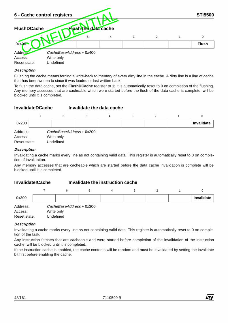
L6 - Cache control registers STi5500
CONFIDENTIAFlushDCache Flush the data cache
Address: CacheBaseAddress + 0x400Access: Write onlyReset state: Undefined
Description
Flushing the cache means forcing a write-back to memory of every dirty line in the cache. A dirty line is a line of cachethat has been written to since it was loaded or last written back. To flush the data cache, set the FlushDCache register to 1; It is automatically reset to 0 on completion of the flushing.Any memory accesses that are cacheable which were started before the flush of the data cache is complete, will beblocked until it is completed.
InvalidateDCache Invalidate the data cache
Address: CacheBaseAddress + 0x200Access: Write onlyReset state: Undefined
DescriptionInvalidating a cache marks every line as not containing valid data. This register is automatically reset to 0 on comple-tion of invalidation. Any memory accesses that are cacheable which are started before the data cache invalidation is complete will beblocked until it is completed.
InvalidateICache Invalidate the instruction cache
Address: CacheBaseAddress + 0x300Access: Write onlyReset state: Undefined
DescriptionInvalidating a cache marks every line as not containing valid data. This register is automatically reset to 0 on comple-tion of the task.Any instruction fetches that are cacheable and were started before completion of the invalidation of the instructioncache, will be blocked until it is completed.If the instruction cache is enabled, the cache contents will be random and must be invalidated by setting the invalidatebit first before enabling the cache.
7 6 5 4 3 2 1 0
0x400 Flush
7 6 5 4 3 2 1 0
0x200 Invalidate
7 6 5 4 3 2 1 0
0x300 Invalidate
48/161 7110599 B
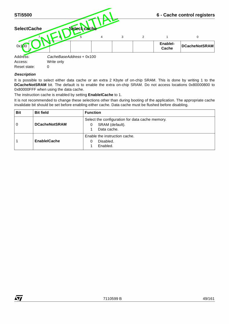
LSTi5500 6 - Cache control registers
CONFIDENTIASelectCache Select cache
Address: CacheBaseAddress + 0x100Access: Write onlyReset state: 0
Description
It is possible to select either data cache or an extra 2 Kbyte of on-chip SRAM. This is done by writing 1 to theDCacheNotSRAM bit. The default is to enable the extra on-chip SRAM. Do not access locations 0x80000800 to0x80000FFF when using the data cache.The instruction cache is enabled by setting EnableICache to 1.It is not recommended to change these selections other than during booting of the application. The appropriate cacheinvalidate bit should be set before enabling either cache. Data cache must be flushed before disabling.
7 6 5 4 3 2 1 0
0x100EnableI-Cache
DCacheNotSRAM
Bit Bit field Function
0 DCacheNotSRAMSelect the configuration for data cache memory.
0 SRAM (default).1 Data cache.
1 EnableICacheEnable the instruction cache.
0 Disabled.1 Enabled.
7110599 B 49/161

L7 - Configuration and control (CFG) registers STi5500
CONFIDENTIA7 Configuration and control (CFG) registers
CFG_CCF Chip Configuration
Address: VideoBaseAddress + 0x01Access: Read/writeReset state: 0Synchronization: Edge triggered
Description
CFG_CDR Compressed Data Input
Address: VideoBaseAddress + 0x44Access: Write onlyReset state: UndefinedSynchronization: None
Description
This register is a compressed data input register. It is used to input compressed data using a different path from theusual DMA path. Depending on the value of CFG_GCF.CDR[1:0] the data stored in this register will enter either theaudio, video or sub-picture compressed data FIFO.
7 6 5 4 3 2 1 0
0x01 EAI EOU PBO EC3 EC2 ECK EDI EVI
Field Bit Description
EAI 7Enable audio interface. When this bit is reset the audio interface is put into its high impedance stateand the internal PCMCLK is disabled. This bit must be set for normal operation and for reducedpower mode (if the display interface is used). It is reset in low power mode.
EOU 6 Enable overflow/underflow errors. When this bit is reset overflow and underflow errors are nottreated internally. This bit must be set for normal operation.
PBO 5Prevent bit buffer overflow. When this bit is set, bit buffer overflow (and thus the loss of data) isprevented by disabling the transfer of data from the compressed data FIFO to the bit bufferwhenever the bit buffer level reaches the threshold defined in the VID_VBT or VID_ABT register.
EC3 4 Enable clock 3. When this bit is reset, the internal clock 3 is disabled. This bit must be set for normaloperation and for reduced power mode. It is reset in low power mode.
EC2 3 Enable clock 2. When this bit is reset, the internal clock 2 is disabled. This bit must be set for normaloperation, and reset in reduced and low power modes.
ECK 2 Enable clocks. When this bit is reset, all internal clocks are disabled. This bit must be set for normaloperation and for reduced power mode. It is reset in low power mode.
EDI 1Enable SDRAM interface. When this bit is reset the SDRAM interface is put into its high impedancestate. This bit must be set for normal operation and for reduced power mode. It is reset in low powermode.
EVI 0Enable video interface. When this bit is reset the video interface is put into its high impedance stateand the internal PIXCLK disabled. This bit must be set for normal operation and for reduced powermode (if the display interface is used). It is reset in low power mode.
7 0
0x44 CFG_CDR[7:0]
50/161 7110599 B
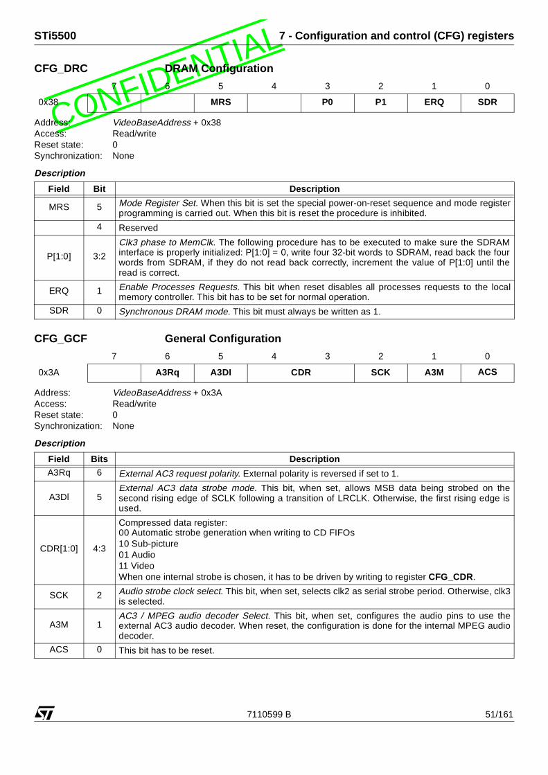
LSTi5500 7 - Configuration and control (CFG) registers
CONFIDENTIACFG_DRC DRAM Configuration
Address: VideoBaseAddress + 0x38Access: Read/writeReset state: 0Synchronization: None
Description
CFG_GCF General Configuration
Address: VideoBaseAddress + 0x3AAccess: Read/writeReset state: 0Synchronization: None
Description
7 6 5 4 3 2 1 0
0x38 MRS P0 P1 ERQ SDR
Field Bit Description
MRS 5 Mode Register Set. When this bit is set the special power-on-reset sequence and mode registerprogramming is carried out. When this bit is reset the procedure is inhibited.
4 Reserved
P[1:0] 3:2
Clk3 phase to MemClk. The following procedure has to be executed to make sure the SDRAMinterface is properly initialized: P[1:0] = 0, write four 32-bit words to SDRAM, read back the fourwords from SDRAM, if they do not read back correctly, increment the value of P[1:0] until theread is correct.
ERQ 1 Enable Processes Requests. This bit when reset disables all processes requests to the localmemory controller. This bit has to be set for normal operation.
SDR 0 Synchronous DRAM mode. This bit must always be written as 1.
7 6 5 4 3 2 1 0
0x3A A3Rq A3DI CDR SCK A3M ACS
Field Bits Description
A3Rq 6 External AC3 request polarity. External polarity is reversed if set to 1.
A3Dl 5External AC3 data strobe mode. This bit, when set, allows MSB data being strobed on thesecond rising edge of SCLK following a transition of LRCLK. Otherwise, the first rising edge isused.
CDR[1:0] 4:3
Compressed data register: 00 Automatic strobe generation when writing to CD FIFOs10 Sub-picture01 Audio11 VideoWhen one internal strobe is chosen, it has to be driven by writing to register CFG_CDR.
SCK 2 Audio strobe clock select. This bit, when set, selects clk2 as serial strobe period. Otherwise, clk3is selected.
A3M 1AC3 / MPEG audio decoder Select. This bit, when set, configures the audio pins to use theexternal AC3 audio decoder. When reset, the configuration is done for the internal MPEG audiodecoder.
ACS 0 This bit has to be reset.
7110599 B 51/161

L7 - Configuration and control (CFG) registers STi5500
CONFIDENTIACFG_MCF Memory Refresh Interval
Address: VideoBaseAddress + 0x00Access: Read/writeReset state: 0Synchronization: none
DescriptionThis register defines the SDRAM refresh interval in units of 32 SDRAM clock periods. For example if 2048 rows mustbe refreshed every 32 ms, with an SDRAM clock of 100 MHz, the following value must be stored in MCF.RFI[6:0]:
(32 x 10-3/2048) x (100 x 106/32) = 48
If the register is set to 0 then refresh is disabled.
7 6 0
0x00 RFI[6:0]
52/161 7110599 B

LSTi5500 8 - Clock generator (CKG) registers
CONFIDENTIA8 Clock generator (CKG) registers
CKG_AUX Clock Generator Auxiliary Clock Divider
Address: VideoBaseAddress + 0x37Access: Serial read/writeReset state: 0
DescriptionThis register controls the fractional divider for the Auxiliary clock. Writing to the highest address (DF) latches the newconfiguration. The bit significance is given in the CKG_CFG register definition below.
CKG_CFG Clock Generator Configuration
Address: VideoBaseAddress + 0x31Access: Read/writeReset state: 0
7 6 5 4 3 0
1st cycle ENA DV2 P0[3:0]
2nd cycle PR[9:3]
3rd cycle PR[2:0] Q[10:7]
4th cycle Q[6:0]
Field Cycle Bits Description
ENA 1 5
Enable. Controls whether or not the fractional divider is enabled or disabled forlow power.
0 fractional divider is disabled1 fractional divider is enabled
DV2 1 4Divide-by-2. The output of the fractional divider is divided by two.
0 not divided by 21 divided by 2.
P0[3:0] 1 3:0 P0. Defines the value of P0 as described in the STi5500 datasheet.
PR[9:3] 2 6:0Pr. Contains the value of Pr as described in the STi5500 datasheet.
PR[2:0] 3 6:4
Q[10:7] 3 3:0 Q. Contains the value of Q as described in the STi5500 datasheet. These bitsshould be programmed to Q (i.e. one’s compliment).Q[6:0] 4 6:0
7 6 0
0x31CKG_CFG[6:0]
7110599 B 53/161

L8 - Clock generator (CKG) registers STi5500
CONFIDENTIADescriptionControls the input/output modes for MEMCLK and PCMCLK and signal selection for MPEG decoders clocks and testmodes. After reset, clock pin PCMCLK is in input mode and clock MEMCLK is in output mode.
CKG_LNK Clock Generator Link Interface Clock Divider
Address: VideoBaseAddress + 0x33Access: Serial read/writeReset state: 0
Description
This register controls the fractional divider for the Link Interface clock. Writing to the highest address (DF) latches thenew configuration. The bits have the significance given in the CKG_CFG register definition.
Field Bit Description
CFG[6] 6
Configuration 6. Controls the input/output state of the MEMCLK pin.
0 the MEMCLK pin is an output from MEMCLKo fractional divider (see bits CKG_MEM.ENA/DV2)1 the MEMCLK can be input externally (bypassing PLL) using the A_C_REQ pin.
CFG[5] 5Configuration 5. Controls the input/output state of the PCMCLK pin.
0 the PCMCLK pin is an input1 the PCMCLK pin is an output from PCMCLKo fractional divider (see bits CKG_PCM.ENA/DV2)
CFG[4:2] 3 Reserved
CFG[1] 1Configuration 1. Selects the Link Iinterface clock.
0Select the external link clock
1Select the the internal divided PLL (see CKG_VID.ENA and CKG_VID.DV2).
CFG[0] 0 Lock bit. This bit is read only. When set to 1, it indicates that the PLL is locked (to be used in PLLinit sequence)
7 6 5 4 3 0
1st cycle ENA DV2 P0[3:0]
2nd cycle PR[9:3]
3rd cycle PR[2:0] Q[10:7]
4th cycle Q[6:0]
Field Cycle Bits Description
ENA 1 5
Enable. Controls whether or not the fractional divider is enabled or disabled forlow power.
0 fractional divider is disabled1 fractional divider is enabled
DV2 1 4Divide-by-2. The output of the fractional divider is divided by two.
0 not divided by 21 divided by 2.
P0[3:0] 1 3:0 P0. Defines the value of P0 as described in the STi5500 datasheet.
PR[9:3] 2 6:0Pr. Contains the value of Pr as described in the STi5500 datasheet.
PR[2:0] 3 6:4
54/161 7110599 B

LSTi5500 8 - Clock generator (CKG) registers
CONFIDENTIA
CKG_MCK Clock Generator SdramClock Divider
Address: VideoBaseAddress + 0x36Access: Serial read/writeReset state: 0
DescriptionThis register controls the fractional divider for the Sdram clock. Writing to the highest address (DF) latches the newconfiguration. The bits have the significance given in the CKG_CFG register definition.
CKG_PCM Clock Generator PCM Clock Divider
Address: VideoBaseAddress + 0x35Access: Serial read/writeReset state: 0
Q[10:7] 3 3:0 Q. Contains the value of Q as described in the STi5500 datasheet. These bitsshould be programmed to Q (i.e. one’s compliment).Q[6:0] 4 6:0
7 6 5 4 3 0
1st cycle ENA DV2 P0[3:0]
2nd cycle PR[9:3]
3rd cycle PR[2:0] Q[10:7]
4th cycle Q[6:0]
Field Cycle Bits Description
ENA 1 5
Enable. Controls whether or not the fractional divider is enabled or disabled forlow power.
0 fractional divider is disabled1 fractional divider is enabled
DV2 1 4Divide-by-2. The output of the fractional divider is divided by two.
0 not divided by 21 divided by 2.
P0[3:0] 1 3:0 P0. Defines the value of P0 as described in the STi5500 datasheet.
PR[9:3] 2 6:0Pr. Contains the value of Pr as described in the STi5500 datasheet.
PR[2:0] 3 6:4
Q[10:7] 3 3:0 Q. Contains the value of Q as described in the STi5500 datasheet. These bitsshould be programmed to Q (i.e. one’s compliment).Q[6:0] 4 6:0
7 6 5 4 3 0
1st cycle ENA DV2 P0[3:0]
2nd cycle PR[9:3]
3rd cycle PR[2:0] Q[10:7]
4th cycle Q[6:0]
Field Cycle Bits Description
7110599 B 55/161

L8 - Clock generator (CKG) registers STi5500
CONFIDENTIADescriptionThis register controls the fractional divider for the PCM clock. Writing to the highest address (DF) latches the new con-figuration. The bits have the significance given in the CKG_CFG register definition.
CKG_PLL Clock Generator PLL Parameters
Address: VideoBaseAddress + 0x30Access: Read/writeReset state: 0
Description
Controls the reference frequency input, pre-divider and multiplication factor of the PLL.The bits have the following significance:
Field Cycle Bits Description
ENA 1 5
Enable. Controls whether or not the fractional divider is enabled or disabled forlow power.
0 fractional divider is disabled1 fractional divider is enabled
DV2 1 4Divide-by-2. The output of the fractional divider is divided by two.
0 not divided by 21 divided by 2.
P0[3:0] 1 3:0 P0. Defines the value of P0 as described in the STi5500 datasheet.
PR[9:3] 2 6:0Pr. Contains the value of Pr as described in the STi5500 datasheet.
PR[2:0] 3 6:4
Q[10:7] 3 3:0 Q. Contains the value of Q as described in the STi5500 datasheet. These bitsshould be programmed to Q (i.e. one’s compliment).Q[6:0] 4 6:0
7 6 5 4 3 0
0x30 PD REF[1:0] N M[3:0]
Field Bits DescriptionPD 7 Power-Down Mode. When set, the reference input to the PLL is reset.
REF[1:0] 6:5
Clock Generator Reference. These bits control the reference frequency input multiplexer tothe clock generator’s PLL.
00 Selects PIXCLK01 Selects PCMCLK10 PLL power down mode11 Selects External Link Clock In
N 4 Divide-by-N+1. When set, the reference input to the PLL is divided by two. This bitcorresponds to N in the STi5500 data sheet.
M[3:0] 3:0PLL Multiplication Factor, M+7. These bits control the reference frequency input to the PLLof the clock generator. The actual multiplication factor is M + 7. This field corresponds to Min the STi5500 data sheet formulae.
56/161 7110599 B

LSTi5500 8 - Clock generator (CKG) registers
CONFIDENTIACKG_PXC Clock Generator Pixel Clock Divider
Address: VideoBaseAddress + 0x34Access: Serial read/writeReset state: 0
DescriptionThis register controls the fractional divider for the Pixel clock. Writing to the highest address (DF) latches the new con-figuration. The bits have the significance given in the CKG_CFG register definition.
7 6 5 4 3 0
1st cycle ENA DV2 P0[3:0]
2nd cycle PR[9:3]
3rd cycle PR[2:0] Q[10:7]
4th cycle Q[6:0]
Field Cycle Bits Description
ENA 1 5
Enable. Controls whether or not the fractional divider is enabled or disabled forlow power.
0 fractional divider is disabled1 fractional divider is enabled
DV2 1 4Divide-by-2. The output of the fractional divider is divided by two.
0 not divided by 21 divided by 2.
P0[3:0] 1 3:0 P0. Defines the value of P0 as described in the STi5500 datasheet.
PR[9:3] 2 6:0Pr. Contains the value of Pr as described in the STi5500 datasheet.
PR[2:0] 3 6:4
Q[10:7] 3 3:0 Q. Contains the value of Q as described in the STi5500 datasheet. These bitsshould be programmed to Q (i.e. one’s compliment).Q[6:0] 4 6:0
7110599 B 57/161

L9 - Digital encoder registers STi5500
CONFIDENTIA9 Digital encoder registers
CCCF1 Closed caption characters/extended data for field 1
Address: DENCBaseAddress + 0x27 and 0x28Access: Read / Write
Description
opc11 is the odd-parity bit of US-ASCII 7-bit character c11[7:1].opc12 is the odd-parity bit of US-ASCII 7-bit character c12[7:1].There is no default value, but closed captions enabling without loading these registers will issue character NULL. cccf1is never reset.
CCCF2 Closed caption characters/extended data for field 2
Address: DENCBaseAddress + 0x29 and 0x2AAccess: Read / Write
Descriptionopc21 is the odd-parity bit of US-ASCII 7-bit character c21[7:1].opc22 is the odd-parity bit of US-ASCII 7-bit character c22[7:1].There is no default value, but closed captions enabling without loading these registers will issue character NULL. cccf2is never reset.
CCLIF1 Closed caption/extended data line insertion for field 1
Address: DENCBaseAddress + 0x2BAccess: Read / Write
DescriptionTV line number where closed caption/extended data is to be encoded in field 1 is programmable through the followingregister:
525/60 system (525-SMPTE line number convention)
Only lines 10 through 22 should be used for closed caption or extended data services (line 1 through 9 contain the ver-tical sync pulses with equalizing pulses).
7 6 5 4 3 2 1 0
0x27 opc11 c117 c116 c115 c114 c113 c112 c111
0x28 opc12 c127 c126 c125 c124 c123 c122 c121
7 6 5 4 3 2 1 0
0x29 opc21 c217 c216 c215 c214 c213 c212 c211
0x2A opc22 c227 c226 c225 c224 c223 c222 c221
7 6 5 4 3 2 1 0
- - - l1_4 l1_3 l1_2 l1_1 l1_0
0x2B 0 0 0 0 1 1 1 1
58/161 7110599 B
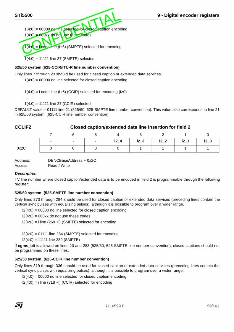
LSTi5500 9 - Digital encoder registers
CONFIDENTIA l1(4:0):= 00000 no line selected for closed caption encoding
l1(4:0):= 000xx do not use these codes
....
l1(4:0):= i code line (i+6) (SMPTE) selected for encoding
....
l1(4:0):= 11111 line 37 (SMPTE) selected
625/50 system (625-CCIR/ITU-R line number convention)
Only lines 7 through 23 should be used for closed caption or extended data services.
l1(4:0):= 00000 no line selected for closed caption encoding
.....
l1(4:0):= i code line (i+6) (CCIR) selected for encoding (i>0)
.....
l1(4:0):= 11111 line 37 (CCIR) selected
DEFAULT value:= 01111 line 21 (525/60, 525-SMPTE line number convention). This value also corresponds to line 21in 625/50 system, (625-CCIR line number convention)
CCLIF2 Closed caption/extended data line insertion for field 2
Address: DENCBaseAddress + 0x2CAccess: Read / Write
Description
TV line number where closed caption/extended data is to be encoded in field 2 is programmable through the followingregister:
525/60 system: (525-SMPTE line number convention)
Only lines 273 through 284 should be used for closed caption or extended data services (preceding lines contain thevertical sync pulses with equalizing pulses), although it is possible to program over a wider range.
l2(4:0):= 00000 no line selected for closed caption encoding
l2(4:0):= 000xx do not use these codes
l2(4:0):= i line (269 +i) (SMPTE) selected for encoding
....
l2(4:0):= 01111 line 284 (SMPTE) selected for encoding
l2(4:0):= 11111 line 289 (SMPTE)
If cgms_bit is allowed on lines 20 and 283 (525/60, 525-SMPTE line number convention), closed captions should notbe programmed on these lines.
625/50 system: (625-CCIR line number convention)
Only lines 319 through 336 should be used for closed caption or extended data services (preceding lines contain thevertical sync pulses with equalizing pulses), although it is possible to program over a wider range.
l2(4:0):= 00000 no line selected for closed caption encoding
l2(4:0):= i line (318 +i) (CCIR) selected for encoding
7 6 5 4 3 2 1 0
- - - l2_4 l2_3 l2_2 l2_1 l2_0
0x2C 0 0 0 0 1 1 1 1
7110599 B 59/161

L9 - Digital encoder registers STi5500
CONFIDENTIA....
l2(4:0):= 10010 line 336 (CCIR) selected for encoding
l2(4:0):= 11111 line 349 (CCIR)
The default value is 01111 line 284 (525/60, 525-SMPTE line number convention). This value also corresponds to line333 in 625/50 system, (625-CCIR line number convention).
CGMS_BIT CGMS data registers
Address: DENCBaseAddress + 0x1F to 0x21Access: Read / write
Description
20 bits only. See the STi5500 datasheet for a description of CGMS encoding. These registers are never reset.
CHIPID DENC identification numberAddress: DENCBaseAddress + 0x11Access: Read only
DescriptionThe value of chipid is 0x0.
CONFIGURATION0 DENC configuration 0
Address: DENCBaseAddress + 0x00Access: Read/writeReset state: 100100102, i.e. NTSC M, ODDEVEN and HSYNC slave mode, synchronized with the rising edge of
ODDEV flags or VSYNC is active low.
7 6 5 4 3 2 1 0
cgms_bit1 0x1F - - - - b1 b2 b3 b4
cgms_bit2 0x20 b5 b6 b7 b8 b9 b10 b11 b12
cgms_bit3 0x21 b13 b14 b15 b16 b17 b18 b19 b20
Field Bits Notes
Word0A b1:3
Word0B b4:6
Word1 b7:10
Word2 b11:14
CRC b15:20 Not internally computed.
Table 9.1 CGMS field encoding
7 6 5 4 3 2 1 0
0x00 std1 std0 sync2 sync1 sync0 polh polv freerun
60/161 7110599 B

LSTi5500 9 - Digital encoder registers
CONFIDENTIADescription
std1-0
The encoding of std1-0 is shown in Table 9.2.The standard on hardware reset is NTSC; any standard modification selects automatically the right parameters for cor-rect subcarrier generation.If bit secam in register configuration7 is set, std1 and std0 bits are not taken into account.
sync2-0
See the STi5500 datasheet for details. The encoding is shown in Table 9.3.
polh
Synchronized with the active edge of HSYNC selection (when input) or polarity of HSYNC (when output)
0 HSYNC is a negative pulse (128 Tckref wide) or falling edge is active. Default.
1 HSYNC is a positive pulse (128 Tckref wide) or rising edge is active.
polv
Synchronized with the active edge of ODDEV/VSYNC selection (when input).
0 Falling edge of ODDEV flags start of field1 (odd field) or VSYNC is active low.
1 Rising edge of ODDEV flags start of field1 (odd field) or VSYNC is active high. Default.
freerun
See the STi5500 datasheet.
0 Disabled. Default.
std1 std0 Standard selected Notes
0 0 PAL BDGHI
0 1 PAL N (see bit set-up)
1 0 NTSC M Default.
1 1 PAL M
Table 9.2 Encoding of std0-1
sync2 sync1 sync0 Configuration Notes
0 0 0 ODDEV-only based slave mode (frame locked)
0 0 1 ‘F’ based slave mode (frame locked)
0 1 0 ODDEV+HSYNC based slave mode (line locked) Default mode.
0 1 1 F+H based slave mode (line locked)
1 0 0 VSYNC-only based slave mode (frame locked) HSYNC is needed as an input. Seesti5500 datasheet.
1 0 1 VSYNC+HSYNC based slave mode (line locked)
1 1 0 Master mode
1 1 1 Autotest mode (color bar pattern)
Table 9.3 Encoding of sync2-0
7110599 B 61/161

L9 - Digital encoder registers STi5500
CONFIDENTIA1 Enabled
NOTE: This bit is taken into account in ODDEV-only, VSYNC-only or F based slave modes and is irrelevant to othersynchronization modes.
CONFIGURATION1 DENC configuration 1
Address: DENCBaseAddress + 0x01Access: Read / Write
Description
blkli
Vertical Blanking Interval selection for active video lines area. See the STi5500 datasheet for details.
0 Partial blanking. Only the following lines inside Vertical Interval are blanked:
NTSC-M lines [1..9], [263(half)..272] (525-SMPTE)
PAL-M lines [523..6], [260(half)..269] (525-CCIR)
other PALlines [623(half)..5], [311..318] (625-CCIR)
This mode allows preservation of VBI data embedded within incoming YCrCb, e.g. Teletext (lines [7..22] and[320..335]), Wide Screen signalling (full line 23), Video Programing Service (line16), etc.)
1 Full blanking. All lines inside VBI are blanked:
NTSC-M lines [1..19], [263(half)..282] (525-SMPTE)
PAL-M lines [523..16], [260(half)..279] (525-CCIR)
other PALlines [623(half)..22], [311..335] (625-CCIR)
Note: blkli must be set to 0 when closed captions and are to be encoded on the following lines:• 525/60before line 20 (SMPTE) or before line 283 (SMPTE)• 625/50before line 23 (CCIR) or before line 336 (CCIR)
flt1-0
U/V Chroma filter bandwidth selection. See the STi5500 datasheet for details.
syncok
Availability of sync signals (analog and digital) in case of input synchronization loss with no free-run active (i.e. fre-erun=0). See the STi5500 datasheet for details.
7 6 5 4 3 2 1 0
blkli flt1 flt0 syncok coki setup cc2 cc1
0x01 0 1 0 0 0 1 0 0
flt1 flt0 3dB bandwidth Typical application
0 0 1.1MHz Low def NTSC filter.
0 1 1.3MHz Low def PAL filter.
1 0 1.6MHzHigh def. NTSC filter (ATSC compliant) and PAL M/N (ITU-R 624.4compliant). Default.
1 1 1.9MHz High def. PAL filter: Rec 624 - 4 for PAL BDG/I compliant.
Table 9.4 Encoding of filt0-1
62/161 7110599 B

LSTi5500 9 - Digital encoder registers
CONFIDENTIA0 No synchro output signals. Default.
1 Output synchros available on YS, CVBS and, when applicable, HSYNC (if output port), ODDEV (if output port), i.e.same behavior as freerun except that video outputs are blanked in the active portion of the line
coki
Color killer. See the STi5500 datasheet for details. For color suppression on chroma DAC ‘C’, see registerconfiguration5 bit bkg_c.
0 Color ON. Default.
1 Color suppressed on CVBS output signal (CVBS=YS) but color still present on C output.
setup
Pedestal enable. See the STi5500 datasheet for details. In all cases, the gain factor is adjusted to obtain the requiredlevels for chrominance.
0 Blanking level and black level are identical on all lines (ex: Argentinian PAL-N, Japan NTSC-M, PAL-BDGHI).
1 Black level is 7.5 IRE above blanking level on all lines outside VBI (ex: Paraguayan and Uruguayan PAL-N).Default.
cc2, cc1
Closed caption encoding mode. See the STi5500 datasheet for details.
CONFIGURATION2 DENC configuration 2
Address: DENCBaseAddress + 0x02 Access: Read / WriteReset state: 001000002, i.e. burst enabled, and all other bits zero.
Description
nintrl
Non-interlaced mode select. See the STi5500 datasheet for details. nintrl update is internally taken into account on thestart of next frame.
0 Interlaced mode (625/50 or 525/60 system). Default.
1 Non-interlaced mode (2x312/50 or 2x262/60 system). Not available in SECAM mode.
enrst
Cyclic update of DDFS phase.
cc2 cc1 Encoding mode
0 0 No closed caption/extended data encoding. Default.
0 1 Closed caption/extended data encoding enabled in field 1 (odd)
1 0 Closed caption/extended data encoding enabled in field 2 (even)
1 1 Closed caption/extended data encoding enabled in both fields
Table 9.5 Encoding of cc2-1
7 6 5 4 3 2 1 0
0x02 nintrl enrst bursten selrst rstosc valrst1 valrst0
7110599 B 63/161

L9 - Digital encoder registers STi5500
CONFIDENTIA0 No cyclic subcarrier phase reset. Default.
1 Cyclic subcarrier phase reset depending of valrst1 and valrst0 (see below).
bursten
Chrominance burst control.
0 Burst is turned off on CVBS, chrominance output is not affected.
1 Burst is enabled. Default.
selrst
Selects set of reset values for Direct Digital Frequency Synthesizer.
0 Hardware reset values for phase and increment of subcarrier oscillator (see description of registersincrement_dfs and phase_dfs for values). Default.
1 Loaded reset values selected (see contents of registers increment_dfs and phase_dfs)
rstosc
Software phase reset of DDFS (Direct Digital Frequency Synthesizer).
0 Default.
1 A 0-to-1 transition resets the phase of the subcarrier to either the hard-wired default phase value or the valueloaded in register phase_dfs (according to bit selrst).
Bit rstosc is automatically set back to 0 after the oscillator reset has been performed.
valrst
Note: valrst[1:0] is taken into account only if bit enrst is set.
Resetting the oscillator means here forcing the value of the phase accumulator to its nominal value to avoid accumulat-ing errors due to the finite number of bits used internally. The value to which the accumulator is reset is either the hard-wired default phase value or the value loaded in registers phase_dfs (according to bit selrst), to which a 00, 900, 1800,or 2700 correction is applied according to the field and line on which the reset is performed.Note: If SECAM is performed the oscillator is reset every line.
CONFIGURATION3 DENC configuration 3
Address: DENCBaseAddress + 0x03Access: Read / WriteReset state: 0
valrst1 valrst0 Selection
0 0 Automatic reset of the oscillator every line. Default.
0 1 Automatic reset of the oscillator every 2nd field.
1 0 Automatic reset of the oscillator every 4th field.
1 1 Automatic reset of the oscillator every 8th field.
Table 9.6 Encoding of valrst
7 6 5 4 3 2 1 0
0x03 entrap trap_pal encgms nosd del2 del1 del0
64/161 7110599 B

LSTi5500 9 - Digital encoder registers
CONFIDENTIADescription
entrap
Enable trap filter.
0 Trap filter disabled. Default.
1 Trap filter enabled.
Note: When SECAM is performed trap filter is always enabled (entrap = 1).
trap_pal
Refer to the STi5500 datasheet for details. trap_pal is taken into account only if bit entrap is set.
0 To select the NTSC trap filter (centered around 3.58 MHz) (See Fig14a). Default.
1 To select the PAL trap filter (centered around 4.43 MHz) (see Fig.14b).
encgms
CGMS encoding enable. (Refer to the STi5500 datasheet for details).
0 Disabled. Default.
1 Enabled.
When encgms is set to 1 Closed-Captions/Extended Data Services should not be programmed on lines 20 and 283.(525/60, SMPTE line number convention).
nosd
Choice of active edge of ckref masterclock that samples incoming YCrCb data. See the STi5500 datasheet.
0 ckref rising edge. Default.
1 ckref falling edge.
del(2:0)
Delay on luma path with reference to chroma path. Table 9.7 shows the encoding, where one pixel at 13.5 MHz corre-sponds to 74.04 ns. Refer to the STi5500 datasheet for details.
del2 del1 del0 Delay on luma path with reference to chroma path
0 1 0 + 2 pixel delay on luma.
0 0 1 + 1 pixel delay on luma.
0 0 0 + 0 pixel delay on luma. Default.
1 1 1 - 1 pixel delay on luma.
1 1 0 - 2 pixel delay on luma.
Others + 0 pixel delay on luma.
Table 9.7 Encoding of del
7110599 B 65/161

L9 - Digital encoder registers STi5500
CONFIDENTIACONFIGURATION4 DENC configuration 4
Address: DENCBaseAddress + 0x04Access: Read / WriteReset state: 0
Description
syncin_ad[1:0]
Adjustment of incoming sync signals. See the STi5500 datasheet for details. Used to insure correct interpretation ofincoming video samples as Y, Cr or Cb when the encoder is slaved to incoming SYNC signals (including ‘F/H’ flagsstripped off ITU-R656/D1 data).
syncout_ad[1:0]
Adjustment of outgoing sync signals. See the STi5500 datasheet for details. Used to insure correct interpretation ofincoming video samples as Y, Cr or Cb when the encoder is master and supplies SYNC signals.
aline
Video active line duration control. See the STi5500 datasheet for details.
0 Full digital video line encoding (720 pixels - 1440 clock cycles)
1 Active line duration follows ITU-R/SMPTE ‘analog’ standard requirements
ttxdel[2:0]
Teletext data latency. The default value is 000. See the STi5500 datasheet for details. The encoder will clock in the firstTeletext data sample on the (2 + ttxdel[2:0])th rising edge of the master clock following the rising edge of TTXS (Tele-text Synchro signal, supplied by the encoder).
7 6 5 4 3 2 1 0
0x04 syncin_ad1 syncin_ad0 syncout_ad1 syncout_ad0 aline ttxdel2 ttxdel1 ttxdel0
syncin_ad1 syncin_ad0 Internal delay undergone by incoming SYNC
0 0 Nominal*. Default.
0 1 +1 external 27 MHz clock cycle
1 0 +2 external 27 MHz clock cycles
1 1 +3 external 27 MHz clock cycles
Table 9.8 Encoding of syncin_ad
syncout_ad1 syncout_ad0 Delay added to sync signals before they are output
0 0 Nominal*. Default.
0 1 +1 external 27 MHz clock cycle
1 0 +2 external 27 MHz clock cycles
1 1 +3 external 27 MHz clock cycles
Table 9.9 Encoding of syncout_ad
66/161 7110599 B

LSTi5500 9 - Digital encoder registers
CONFIDENTIACONFIGURATION5 DENC configuration 5
Address: DENCBaseAddress + 0x05Access: Read / WriteReset state: 001100002, i.e. C and Y DACS at neutral.
Description
bkcvbs
Blanking of DAC CVBS
0 DAC N in normal operation. Default.
1 DAC N input code forced to blanking level.
bkys
Blanking of DAC’Y’
0 DAC G/Y in normal operation.
1 DAC G/Y input code forced to blanking level. Default.
bkc
Blanking of DAC ’C’
0 DAC R/C in normal operation.
1 DAC R/C input code forced to neutral level, i.e. no color. Default.
bkr
Blanking of DAC ’R’
0 DAC R in normal operation.
1 DAC R input code forced to black level.
bkg
Blanking of DAC ’G’
0 DAC G in normal operation.
1 DAC G input code forced to black level.
bkb
Blanking of DAC ’B’
0 DAC B/CVBS in normal operation. Default.
1 DAC B/CVBS input code forced to black level.
dacinv
Inverts DAC codes to compensate for an inverting output stage in the application.
0 DAC non-inverted inputs. Default.
1 DAC inverted inputs.
7 6 5 4 3 2 1 0
0x05 - bkcvbs bkys bkc bkr bkg bkb dacinv
7110599 B 67/161

L9 - Digital encoder registers STi5500
CONFIDENTIACONFIGURATION6 DENC configuration 6
Address: DENCBaseAddress + 0x06Access: Read / WriteReset state: 000100002
Description
softreset
Software reset
0 No reset. Default.
1 Software reset.
Note: Bit softreset is automatically reset after internal reset generation.Software reset is active during 4 CKREF periods.When softreset is activated, all the device is reset as with hardware reset except for the first eight user registers(configuration0-7) and for registers increment_dfs, phase_dfs (increment and phase of oscillator), cgms_bit,ttx_blockn and ccf1-2.
jump, dec_ninc and free_jump
See the description of line insertion and line skipping in the STi5500 datasheet.
Bit jump is automatically reset after use.
7 6 5 4 3 2 1 0
0x06 softreset jump dec_ninc free_jump cfc1 cfc0 - maxdyn
jump dec_ninc free_jump Update mode
0 0 0
Normal mode (no line skip or insert capability).
ITU-R (CCIR): 313/312 or 263/262.
Non-interlaced: 312/312 or 262/262.
0 x 1
Manual mode for line insert (dec_ninc = 0) or skip (dec_ninc = 1) capability. This isthe default mode. Both fields of all the frames following the writing of this value aremodified according to Iref and Itarg bits of registers line_reg. By default Iref=0 andItarg=1 which leads to the normal mode above.
1 0 0Automatic line insert mode. The second field of the frame following the writing of thisvalue is increased. In 525/60, two lines are inserted after line 245. In 625/50, fourlines are inserted after line 290. Iref and Itarg are ignored.
1 1 0
Automatic line skip mode. The second field of the frame following the writing of thisvalue is decreased. In 525/60, two lines are skipped after line 245. In 625/50, fourlines are skipped after line 290. Iref and Itarg are ignored. Two lines are skipped(inserted) in 525/60 and four in 625/50 mode.
1 x 1 Reserved. Do not use.
68/161 7110599 B

LSTi5500 9 - Digital encoder registers
CONFIDENTIAcfc1-0
Color frequency control via CFC line.
maxdyn
Maximum dynamic magnitude allowed on YCrCb inputs for encoding. (Refer to the STi5500 datasheet for details.)
0 0x10 to 0xEB for Y, 0x10 to 0xE0 for chrominance (Cr, Cb). Default.1 0x01 to 0xFE for Y, Cr and Cb
Note: in any case, EAV and SAV words are replaced by blanking values before being fed to the luminance and chromi-nance processors.
INCREMENT_DFS DENC Increment for Digital Frequency Synthesizer
Address: DENCBaseAddress + 0x0A, 0x0B, 0x0CAccess: Read / Write
Description
These registers contain the 24-bit increment used by the DDFS if bit selrst equals 1 to generate the phase of the sub-carrier i.e. the address that is supplied to the sine ROM. It therefore allows to customize the subcarrier frequency syn-thesized. Refer to the STi5500 datasheet for details. 1 LSB ~ 1.6 Hz The procedure to validate usage of these registers instead of the hard-wired values is the following:
• Load the registers with the required value;• Set bit selrst in configuration2 to 1;• Perform a software reset using configuration6.
Notes:
1 The values loaded in increment_dfs are taken into account after a software reset, and ONLY IF bit selrst =1.2 These registers are never reset and must be explicitly written into to contain sensible information. 3 On hardware reset (selrst = 0) or on soft reset with selrst=0, the DDFS is initialized with a hard wired increment,
independent of increment_dfs. These hard wired values being out of any user register these cannot be read outof the DENC. These values are given in Table 9.11.
cfc2 cfc1 Update mode
0 0 Disabled. Update is done by loading the increment_dfs registers. Default.
0 1 Update of increment for DDFS just after serial loading via CFC.
1 0 Update of increment for DDFS on next active edge of HSYNC.
1 1 Update of increment for DDFS just before next color burst.
Table 9.10 Encoding of cfc
7 6 5 4 3 2 1 0
0x0A d23 d22 d21 d20 d19 d18 d17 d16
0x0B d15 d14 d13 d12 d11 d10 d9 d8
0x0C d7 d6 d5 d4 d3 d2 d1 d0
7110599 B 69/161

L9 - Digital encoder registers STi5500
CONFIDENTIA
LINE_REG Line jump
Address: DENCBaseAddress + 0x15, 0x16, 0x17Access: Read / write
DescriptionThese registers may be used to jump from a reference line (end of that line) to a target line of the SAME FIELD.However, not all lines can be skipped or repeated with no problems and, if needed, this functionality should BE USEDWITH CAUTION.lref[8:0] contains in binary format the reference line from which a jump is required. ltarg[8:0] contains the target linebinary number.Default values: lref[8:0]:= 000000000 and ltarg[8:0]:= 000000001
PHASE_DFS Static phase offset for digital frequency synthesizer
Address: DENCBaseAddress + 0x0D, 0x0EAccess: Read / write
Description
Under certain circumstances (detailed below), these registers contain the 10 most significant bits of the value withwhich the phase accumulator of the DDFS is initialized after a 0-to-1 transition of bit rstosc (configuration2), or aftera standard change, or when cyclic phase readjustment has been programmed (see bits valrst[1:0] ofconfiguration2). The 14 remaining bits loaded into the accumulator in these cases are all ‘0’s. This allows the defini-tion of the phase reset value to within a 0.35o accuracy.The procedure to validate usage of these registers instead of the hard-wired values is:
• Load the registers with the required value• Set bit selrst to 1 in configuration2• Perform a software reset (in configuration6)
Notes:
1 Registers phase_dfs are never reset and must be explicitly written to before they contain sensible information.
Value of d[23:0] Standard Frequency synthesized Ref. Clock
0x21F07C NTSC M 3.5795452 MHz 27 MHz
0x2A098B PAL BGHIN 4.43361875MHz 27 MHz
0x21F694 PAL N 3.5820558 MHz 27 MHz
0x21E6F0 PAL M 3.57561149 MHz 27 MHz
Table 9.11 Hard wired increment after hardware reset
7 6 5 4 3 2 1 0
0x15 ltarg8 ltarg7 ltarg6 ltarg5 ltarg4 ltarg3 ltarg2 ltarg1
0x16 ltarg0 lref8 lref7 lref6 lref5 lref4 lref3 lref2
0x17 lref1 lref0 - - - - - -
7 6 5 4 3 2 1 0
phase_dfs1 0x0D - - - - - - o23 o22
phase_dfs2 0x0E o21 o20 o19 o18 o17 o16 o15 o14
70/161 7110599 B

LSTi5500 9 - Digital encoder registers
CONFIDENTIA2 If bit selrst = 0 (e.g. after a hardware reset) the phase offset used every time the DDFS is reinitialized is a hard-
wired value. The hard-wired values being out of any register, they cannot be read out of the DENC. These are:
0xD9C000 for PAL BDGHI, N, M,
0x1FC000 for NTSC-M.
revid Digital encoder revision numberAddress: DENCBaseAddress + 0x12Access: Read only
Description
The value of revid is 0x0.
STATUS DENC Status
Address: DENCBaseAddress + 0x09Access: Read only
Description
hok
Hamming decoding of frame sync flag embedded within ITU-R656 / D1 compliant YCrCb streams
0 Consecutive errors.
1 A single or no error. Default.
Note: signal quality detector is issued from Hamming decoding of EAV,SAV from YCrCb
atfr
Frame synchronization flag
0 Encoder not synchronized. Default.
1 In slave mode: encoder synchronized.
buf2_free
Closed caption registers access condition for field 2. (Refer to the STi5500 datasheet for details.)Closed caption data for field 2 is buffered before being output on the relevant TV line; buf2_free is reset if the buffer istemporarily unavailable. If the microcontroller can guarantee that register cccf2 is never written more than oncebetween two frame reference signals, then bit buf2_free will always be true (set). Otherwise, closed caption field 2registers access might be temporarily forbidden by resetting bit buf2_free until the next field 2 closed caption lineoccurs.Note that this bit is false (reset) when 2 pairs of data bytes are awaiting to be encoded, and is set back immediatelyafter one of these pairs has been encoded (so at that time, encoding of the last pair of bytes is still pending).The default value is 1 (access authorized).
buf1_free
Closed caption registers access condition for field 1Same as buf2_free but concerns field 1.
7 6 5 4 3 2 1 0
0x09 hok atfr buf2_free buf1_free fieldct2 fieldct1 fieldct0 jump
7110599 B 71/161

L9 - Digital encoder registers STi5500
CONFIDENTIAThe default value is 1 (access authorized).
fieldct[2:0]
Digital field identification number
000 Indicates field 1
...
111 Indicates field 8
fieldct[0] also represents the odd/even information (odd=0, even=1).
jump
Indicates whether a frame length modification has been programmed at 1 from programming of bit jump to the end ofany frames concernedThe default value is 0.Refer to registers configuration6 and line_reg.
ttx_block1-4 Teletext block definition
Address: DENCBaseAddress + 0x22 (block1) to 0x25 (block4)Access: Read / Write
Description
The use of these registers is described in the STi5500 datasheet These four Teletext Block Definition registers areused in conjunction with the Teletext Block Mapping register ttx_block_map. Refer to the STi5500 datasheet fordetails. Each of these registers defines a start line (txbsn[3:0]) and an end line (txben[3:0]). txbsn is the TeletextBlock Start for block n, and txben is the Teletext Block End for block n.For n = 1, 2, 3 and 4:
txbsn[3:0] = i codes line (7 + i) when applying to field1,
txbsn[3:0] = i codes line (320 + i) when applying to field2.
The end lines are coded in a similar manner.Line numbering is according to ITU-R601/625.There is no default value; registers ttx_block1-4 are never reset.
ttx_block_map Teletext Block Mapping
Address: DENCBaseAddress + 0x26Access: Read / write
7 6 5 4 3 2 1 0
ttx_block1 0x22 txbs1.3 txbs1.2 txbs1.1 txbs1.0 txbe1.3 txbe1.2 txbe1.1 txbe1.0
ttx_block2 0x23 txbs2.3 txbs2.2 txbs2.1 txbs2.0 txbe2.3 txbe2.2 txbe2.1 txbe2.0
ttx_block3 0x24 txbs3.3 txbs3.2 txbs3.1 txbs3.0 txbe3.3 txbe3.2 txbe3.1 txbe3.0
ttx_block4 0x25 txbs4.3 txbs4.2 txbs4.1 txbs4.0 txbe4.3 txbe4.2 txbe4.1 txbe4.0
7 6 5 4 3 2 1 0
0x26 txmf1.1 txmf1.2 txmf1.3 txmf1.4 txmf2.1 txmf2.2 txmf2.3 txmf2.4
72/161 7110599 B

LSTi5500 9 - Digital encoder registers
CONFIDENTIADescriptiontxmf1 stands for Teletext blocks mapping to field1 and txmf2 stands for Teletext blocks Mapping to field 2.This register allows the mapping of the blocks of Teletext lines defined by registers 34 to 37 to either field1, field 2 orboth. Its default value is 0.txmf1.N defines whether txbdN applies to field 1, where txbdN means the Nth teletext block, as described under reg-isters ttx_block1-4. Similarly txmf2.N defines whether txbdN applies to field 2. In other words, if txmf1.N = 1 thenTeletext will be encoded in field 1 from the line defined by txbsN.[3:0] (see above) to the line defined by txbeN.[3:0]. Similarly, if txmf2.N = 1 then Teletext will be encoded in field 2 from the line defined txbsN.[3:0] (see above) to the linedefined by txbeN.[3:0].
7110599 B 73/161

L10 - External memory interface (EMI) registers STi5500
CONFIDENTIA10 External memory interface (EMI) registers
EMIConfigData0 EMI configuration data register 0
DRAM format
SRAM/peripheral format
Address: EMIBaseAddress + 0x00, 0x10, 0x20 and 0x30Access: Read/writeReset state: See Table 10.2.
DescriptionEMI configuration data register 0 for banks 0 to 3. There is one of these configuration registers for each bank. For safeconfiguration, each of the four banks should be configured after reset and then have their configuration locked by writ-ing to the EMIConfigLock register before any access to an external bank is made.The format of the configuration registers for a bank depends on the memory device type, i.e. whether the bank is con-figured for DRAM or for SRAM and peripherals. The type is defined by the DeviceType field in this register.
15 14 13 12 11 10 9 8 7 6 5 4 3 2 1 0
Bank0 0x00DataDrive
DelayBusRelease
TimeSub
BanksSubBank
SizeShiftAmount DeviceType
Bank1 0x10DataDrive
DelayBusRelease
TimeSub
BanksSubBank
SizeShiftAmount DeviceType
Bank2 0x20DataDrive
DelayBusRelease
TimeSub
BanksSubBank
SizeShiftAmount DeviceType
Bank3 0x30DataDrive
DelayBusRelease
TimeSub
BanksSubBank
SizeShiftAmount DeviceType
15 14 13 12 11 10 9 8 7 6 5 4 3 2 1 0
Bank0 0x00 DataDriveDelayBusRelease
TimeCSActive OEActive WEActive DeviceType
Bank1 0x10 DataDriveDelayBusRelease
TimeCSActive OEActive WEActive DeviceType
Bank2 0x20 DataDriveDelayBusRelease
TimeCSActive OEActive WEActive DeviceType
Bank3 0x30 DataDriveDelayBusRelease
TimeCSActive OEActive WEActive DeviceType
Bit Bit field Function
15:14 Reserved Write 0.
13 DataDriveDelay Data drive delay; 0-1 phases
12 BusReleaseTime Bus release time; 0 means 1 cycle, 1 means 2 cycles
Table 10.1 EMI configuration data register 0 format for DRAM
74/161 7110599 B

LSTi5500 10 - External memory interface (EMI) registers
CONFIDENTIA
11:10 SubBanks
00 no sub-banks01 2 sub-banks10 4 sub-banks11 reserved
9:8 SubBankSize
00 256k words01 1M words10 4M words11 16M words
7:5 ShiftAmount Column address width (0 means 7 bits, 1 means 8 bits etc.)
4:3 Reserved Write 0.
2:0 DeviceType 000 = DRAM. Sets the format of the configuration registers for the bank.
Bit Bit field Function Reset
15:13 DataDriveDelay Data drive delay; 0-7 phases 5
12:11 BusReleaseTime Bus release time; 0-3 cycles 2
10:9 CSactive See Table 10.3 01
8:7 OEactive See Table 10.3 01
6:5 WEactive See Table 10.3 00
4:3 Reserved Write 0
2:0 DeviceType 1 = SRAM/peripheral. Sets the format of the configuration registers forthe bank.
1
Table 10.2 EMI configuration data register 0 format for SRAM/Peripherals
Active bit settings Strobe activity
00 Strobe inactive.
01 Strobe active during read accesses only.
10 Strobe active during write accesses only.
11 Strobe active during read and write accesses.
Table 10.3 Active bit settings
Bit Bit field Function
Table 10.1 EMI configuration data register 0 format for DRAM
7110599 B 75/161

L10 - External memory interface (EMI) registers STi5500
CONFIDENTIAEMIConfigData1 EMI configuration data register 1
DRAM format
SRAM/peripheral format
Address: EMIBaseAddress + 0x04, 0x14, 0x24 and 0x34Access: Read/writeReset state: See Table 10.5.
Description
EMI configuration data register 1 for banks 0 to 3. There is one of these configuration registers for each bank. For safeconfiguration, each of the four banks should be configured after reset and then have their configuration locked by writ-ing to the EMIConfigLock register before any access to an external bank is made.The format of the configuration registers for a bank depends on the memory device type, i.e. whether the bank is con-figured for DRAM or for SRAM and peripherals. The type is defined by the DeviceType field in registerEMIConfigData0.
15 14 13 12 11 10 9 8 7 6 5 4 3 2 1 0
Bank0 0x04 RASbits[22:7]
Bank1 0x14 RASbits[22:7]
Bank2 0x24 RASbits[22:7]
Bank3 0x34 RASbits[22:7]
15 14 13 12 11 10 9 8 7 6 5 4 3 2 1 0
Bank0 0x04 AccessTimeReadCSe1Time
ReadCSe2Time
ReadOEe1Time
ReadOEe2Time
ReadWEe1Time
ReadWEe2Time
Read
Bank1 0x14 AccessTimeReadCSe1Time
ReadCSe2Time
ReadOEe1Time
ReadOEe2Time
ReadWEe1Time
ReadWEe2Time
Read
Bank2 0x24 AccessTimeReadCSe1Time
ReadCSe2Time
ReadOEe1Time
ReadOEe2Time
ReadWEe1Time
ReadWEe2Time
Read
Bank3 0x34 AccessTimeReadCSe1Time
ReadCSe2Time
ReadOEe1Time
ReadOEe2Time
ReadWEe1Time
ReadWEe2Time
Read
Bit Bit field Function
15:0 RASbits[22:7] Page address mask for address bits 22:7
Table 10.4 EMI configuration data register 1 format for DRAM
Bit Bit field Function Reset
15:12 AccessTimeRead 2 cycles + 0-15 cycles 8
11:10 CSe1TimeRead Delay of falling edge of CS in3 phases after start of access cycle 0
9:8 CSe2TimeRead Delay from rising edge of CS in phases before end of access cycle 0
7:6 OEe1TimeRead Delay of falling edge of OE in phases after start of access cycle 0
Table 10.5 EMI configuration data register 1 format for SRAM
76/161 7110599 B

LSTi5500 10 - External memory interface (EMI) registers
CONFIDENTIA
EMIConfigData2 EMI configuration data register 2
DRAM format
SRAM/peripheral format
Address: EMIBaseAddress + 0x08, 0x18, 0x28 and 0x38Access: Read/writeReset state: See Table 10.7.
DescriptionEMI configuration data register 2 for banks 0 to 3. There is one of these configuration registers for each bank. For safeconfiguration, each of the four banks should be configured after reset and then have their configuration locked by writ-ing to the EMIConfigLock register before any access to an external bank is made.The format of the configuration registers for a bank depends on the memory device type, i.e. whether the bank is con-figured for DRAM or for SRAM and peripherals. The type is defined by the DeviceType field in registerEMIConfigData0.
5:4 OEe2TimeRead Delay from rising edge of OE in phases before end of access cycle 0
3:2 WEe1TimeRead Delay of falling edge of WE in phases after start of access cycle 0
1:0 WEe2TimeRead Delay from rising edge of WE in phases before end of access cycle 0
15 14 13 12 11 10 9 8 7 6 5 4 3 2 1 0
Bank0 0x08 RASbits[29:23] PrechargeTime RefreshIntervalRefresh
RASedge
Bank1 0x18 RASbits[29:23] PrechargeTime RefreshIntervalRefresh
RASedge
Bank2 0x28 RASbits[29:23] PrechargeTime RefreshIntervalRefresh
RASedge
Bank3 0x38 RASbits[29:23] PrechargeTime RefreshIntervalRefresh
RASedge
15 14 13 12 11 10 9 8 7 6 5 4 3 2 1 0
Bank0 0x08 AccessTimeWriteCSe1Time
WriteCSe2Time
WriteOEe1Time
WriteOEe2Time
WriteWEe1Time
WriteWEe2Time
Write
Bank1 0x18 AccessTimeWriteCSe1Time
WriteCSe2Time
WriteOEe1Time
WriteOEe2Time
WriteWEe1Time
WriteWEe2Time
Write
Bank2 0x28 AccessTimeWriteCSe1Time
WriteCSe2Time
WriteOEe1Time
WriteOEe2Time
WriteWEe1Time
WriteWEe2Time
Write
Bank3 0x38 AccessTimeWriteCSe1Time
WriteCSe2Time
WriteOEe1Time
WriteOEe2Time
WriteWEe1Time
WriteWEe2Time
Write
Bit Bit field Function Reset
Table 10.5 EMI configuration data register 1 format for SRAM
7110599 B 77/161

L10 - External memory interface (EMI) registers STi5500
CONFIDENTIA
EMIConfigData3 EMI configuration data register 3
DRAM format
SRAM/peripheral format
Bit Bit field Function
15 Reserved Write 0
14:8 RASBits[29:23] Page address mask for address bits 29:23
7:5 PrechargeTime 1 to 8 cycles
4:1 RefreshInterval 1 to 16 periods of 128 cycles
0 RefreshRASedge 0 means 1 cycle or 1 means 2 cycles after start of refresh
Table 10.6 EMI configuration data register 2 register format for DRAM
Bit Bit field Function
15:12 AccessTimeWrite 2 cycles + 0-15 cycles
11:10 CSe1TimeWrite Delay of falling edge of CS in phases after start of access cycle
9:8 CSe2TimeWrite Delay from rising edge of CS in phases before end of access cycle
7:6 OEe1TimeWrite Delay of falling edge of OE in phases after start of access cycle
5:4 OEe2TimeWrite Delay from rising edge of OE in phases before end of access cycle
3:2 WEe1TimeWrite Delay of falling edge of WE in phases after start of access cycle
1:0 WEe2TimeWrite Delay from rising edge of WE in phases before end of access cycle
Table 10.7 EMI configuration data register 2 register format for SRAM
15 14 13 12 11 10 9 8 7 6 5 4 3 2 1 0
Bank0 0x0CRAStime
CAStimeRAS
e1TimeRASe2Time CASe1Time CASe2Time
Multibyte
LatchPoint
Bank1 0x1CRAStime
CAStimeRAS
e1TimeRASe2Time CASe1Time CASe2Time
Multibyte
LatchPoint
Bank2 0x2CRAStime
CAStimeRAS
e1TimeRASe2Time CASe1Time CASe2Time
Multibyte
LatchPoint
Bank3 0x3CRAStime
CAStimeRAS
e1TimeRASe2Time CASe1Time CASe2Time
Multibyte
LatchPoint
15 14 13 12 11 10 9 8 7 6 5 4 3 2 1 0
Bank0 0x0C LatchPoint
Bank1 0x1C LatchPoint
Bank2 0x2C LatchPoint
Bank3 0x3C LatchPoint
78/161 7110599 B

LSTi5500 10 - External memory interface (EMI) registers
CONFIDENTIAAddress: EMIBaseAddress + 0x0C, 0x1C, 0x2C and 0x3CAccess: Read/writeReset state: 0
Description
EMI configuration data register 3 for banks 0 to 3. There is one of these configuration registers for each bank. For safeconfiguration, each of the four banks should be configured after reset and then have their configuration locked by writ-ing to the EMIConfigLock register before any access to an external bank is made.The format of the configuration registers for a bank depends on the memory device type, i.e. whether the bank is con-figured for DRAM or for SRAM and peripherals. The type is defined by the DeviceType field in registerEMIConfigData0.
EMIConfigLockBank3-0 EMI configuration lock
Address: EMIBaseAddress + 0x40 to 0x4CAccess: Write onlyReset state: 0
Bit Bit field Function
15:12 Reserved Write 0
11 RAStime 1 or 2 cycles
10:9 CAStime 2 cycles + 0-3 cycles
8 RASe1Time Falling edge of RAS. 1-2 phases after start of RASTime
7:6 RASe2Time Rising edge of RAS. 0-3 phases before end of CASTime
5:4 CASe1Time Falling edge of CAS. 1-4 phases after start of CASTime
3:2 CASe2Time Rising edge of CAS. 0-3 phases before end of CASTime
1 Multibyte When set, enables byte addressing using CAS strobes (byte mode)
0 LatchPoint0 end of CASTime1 1 cycle before end of CASTime
Table 10.8 EMI configuration data register 3 format for DRAM
Bit Bit field Function Reset
15:2 Reserved Write 0
1:0 LatchPoint0 end of access cycle1 1 cycle before end of access cycle2 2 cycles before end of access cycle
0
Table 10.9 EMI configuration data register 3 format for SRAM and peripherals
15 14 13 12 11 10 9 8 7 6 5 4 3 2 1 0
0x40 Lock0
0x44 Lock1
0x48 Lock2
0x4C Lock3
7110599 B 79/161
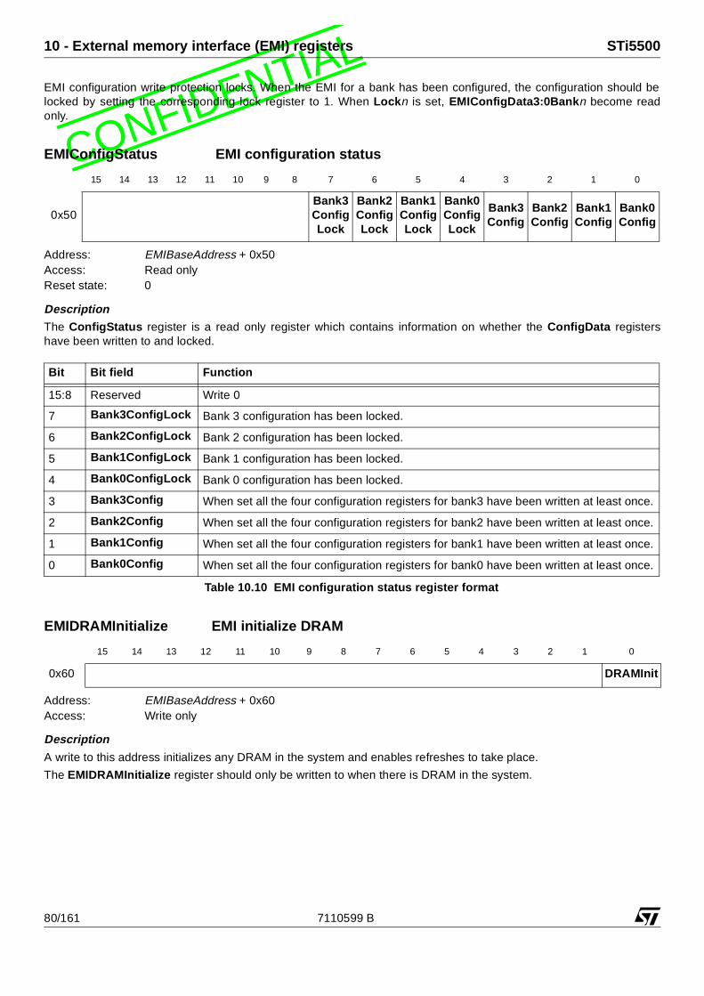
L10 - External memory interface (EMI) registers STi5500
CONFIDENTIAEMI configuration write protection locks. When the EMI for a bank has been configured, the configuration should belocked by setting the corresponding lock register to 1. When Lockn is set, EMIConfigData3:0Bankn become readonly.
EMIConfigStatus EMI configuration status
Address: EMIBaseAddress + 0x50Access: Read onlyReset state: 0
DescriptionThe ConfigStatus register is a read only register which contains information on whether the ConfigData registershave been written to and locked.
EMIDRAMInitialize EMI initialize DRAM
Address: EMIBaseAddress + 0x60Access: Write only
Description
A write to this address initializes any DRAM in the system and enables refreshes to take place.
The EMIDRAMInitialize register should only be written to when there is DRAM in the system.
15 14 13 12 11 10 9 8 7 6 5 4 3 2 1 0
0x50Bank3ConfigLock
Bank2ConfigLock
Bank1ConfigLock
Bank0ConfigLock
Bank3Config
Bank2Config
Bank1Config
Bank0Config
Bit Bit field Function
15:8 Reserved Write 0
7 Bank3ConfigLock Bank 3 configuration has been locked.
6 Bank2ConfigLock Bank 2 configuration has been locked.
5 Bank1ConfigLock Bank 1 configuration has been locked.
4 Bank0ConfigLock Bank 0 configuration has been locked.
3 Bank3Config When set all the four configuration registers for bank3 have been written at least once.
2 Bank2Config When set all the four configuration registers for bank2 have been written at least once.
1 Bank1Config When set all the four configuration registers for bank1 have been written at least once.
0 Bank0Config When set all the four configuration registers for bank0 have been written at least once.
Table 10.10 EMI configuration status register format
15 14 13 12 11 10 9 8 7 6 5 4 3 2 1 0
0x60 DRAMInit
80/161 7110599 B

LSTi5500 11 - Interrupt controller registers
CONFIDENTIA11 Interrupt controller registers
Clear_Exec Clear a bit of the Exec register
Address: IntControllerBase + 0x108Access: Write only
Description
Clear_Exec allows bits of Exec to be cleared individually. Writing a ‘1’ in this register resets the corresponding bit inthe Exec register, a ‘0’ leaves the bit unchanged.
Clear_Mask Clear a bit of the interrupt enable mask
Address: IntControllerBase + 0xC8Access: Write only
Description
Clear_Mask allows bits of Mask to be cleared individually. Writing a ‘1’ in this register resets the corresponding bit inthe Mask register, a ‘0’ leaves the bit unchanged.
Clear_Pending Clear a bit of the Pending register
Address: IntControllerBase + 0x88Access: Write only
Description
Clear_Pending allows bits of Pending to be cleared individually. Writing a ‘1’ in this register resets the correspondingbit in the Pending register, a ‘0’ leaves the bit unchanged.
Exec Interrupts executing
Address: IntControllerBase + 0x100Access: Read/writeReset state: 0
Description
The Exec register keeps track of the currently executing and preempted interrupts. A bit is set when the CPU startsrunning code for that interrupt. The highest priority interrupt bit is reset once the interrupt handler executes a return
31 30 29 28 28 26 25 24 23 22 21 20 19 18 17 16 15 14 13 12 11 10 9 8 7 6 5 4 3 2 1 0
0x108 Clr
Clr
Clr
Clr
Clr
Clr
Clr
Clr
Clr
31 30 29 28 28 26 25 24 23 22 21 20 19 18 17 16 15 14 13 12 11 10 9 8 7 6 5 4 3 2 1 0
0xC8 Clr
Clr
Clr
Clr
Clr
Clr
Clr
Clr
Clr
31 30 29 28 28 26 25 24 23 22 21 20 19 18 17 16 15 14 13 12 11 10 9 8 7 6 5 4 3 2 1 0
0x88 Clr
Clr
Clr
Clr
Clr
Clr
Clr
Clr
Clr
31 30 29 28 28 26 25 24 23 22 21 20 19 18 17 16 15 14 13 12 11 10 9 8 7 6 5 4 3 2 1 0
0x100
IntE
x7
IntE
x6
IntE
x5
IntE
x4
IntE
x3
IntE
x2
IntE
x1
IntE
x0
7110599 B 81/161

L11 - Interrupt controller registers STi5500
CONFIDENTIAfrom interrupt (iret). The Exec register is mapped onto two additional addresses Set_Exec and Clear_Exec so thatbits can be set or cleared individually.
HandlerWptrn Interrupt handler work space pointer
Address: IntControllerBase + 0x00 to 0x1CAccess: Read/writeReset state: Undefined
Description
The HandlerWptr registers (1 per interrupt level) each contain a pointer to the work space of the corresponding inter-rupt handler. The base of the work space is 32-bit word aligned, so the two least significant bits of the 32-bit addressare always zero, and are not held. Each register also contains a priority bit P which determines whether the interrupt isat a higher or lower priority than the high priority process queue.Before the interrupt is enabled by writing a 1 in the Mask register, the software must ensure that there is a valid Han-dlerWptr in the register.
Mask Interrupt enable mask
Address: IntControllerBase + 0xC0Access: Read/write
31 30 29 28 28 26 25 24 23 22 21 20 19 18 17 16 15 14 13 12 11 10 9 8 7 6 5 4 3 2 1 0
0x00 HandlerWptr0[31:2] P
0x04 HandlerWptr1[31:2] P
0x08 HandlerWptr2[31:2] P
0x0C HandlerWptr3[31:2] P
0x10 HandlerWptr4[31:2] P
0x14 HandlerWptr5[31:2] P
0x18 HandlerWptr6[31:2] P
0x1C HandlerWptr7[31:2] P
Bit field Bit Function
HandlerWptr[31:2] 31:2 The 30 most significant bits of the address of the work space of the interrupt handler.
1 Reserved, write 0.
P 0
Sets the priority of the interrupt. If this bit is set to 0, the interrupt is a higher priority thanthe high priority process queue; if this bit is 1, the interrupt is a lower priority than thehigh priority process queue.
0 high priority1 low priority
Table 11.1 HandlerWptrn register format, one register per input
31 30 29 28 28 26 25 24 23 22 21 20 19 18 17 16 15 14 13 12 11 10 9 8 7 6 5 4 3 2 1 0
0xC0
Glo
En
IntE
n7
IntE
n6
IntE
n5
IntE
n4
IntE
n3
IntE
n2
IntE
n1
IntE
n0
82/161 7110599 B

LSTi5500 11 - Interrupt controller registers
CONFIDENTIAReset state: 0
DescriptionAn interrupt mask register is provided in the interrupt controller to selectively enable or disable external interrupts. Thismask register also includes a global interrupt disable bit to disable all external interrupts whatever the state of the indi-vidual interrupt mask bits.To complement this the interrupt controller also includes an interrupt pending register which contains a pending flag foreach interrupt channel. The Mask register performs a masking function on the Pending register to give control overwhat is allowed to interrupt the CPU while retaining the ability to continually monitor external interrupts.On start-up, the Mask register is initialized to zeros, so all interrupts are disabled, both globally and individually. Whena 1 is written to the GlobalEnable bit, the individual interrupt channels are still disabled. To enable an interrupt chan-nel, a 1 must also be written to the corresponding InterruptEnable bit.
The Mask register is mapped onto two additional addresses Set_Mask and Clear_Mask so that bits can be set orcleared individually.
Pending Interrupt pending
Address: IntControllerBase + 0x80Access: Read/writeReset state: 0
Description
The Pending register contains one bit per interrupt level with each bit controlled by the corresponding interrupt. A readcan be used to examine the state of the interrupt controller while a write can be used to explicitly trigger an interrupt.A bit is set when the triggering condition for an interrupt is met. All bits are independent so that several bits can be setin the same cycle. Once a bit is set, a further triggering condition will have no effect. The triggering condition is inde-pendent of the Mask register.The highest priority interrupt bit is reset once the interrupt controller has made an interrupt request to the CPU.The interrupt controller receives external interrupt requests and makes an interrupt request to the CPU when it has apending interrupt request of higher priority than the currently executing interrupt handler.If the software needs to write or clear some bits of the Pending register, the interrupts should be masked (by writing orclearing the Mask register) before writing or clearing the Pending register. The interrupts can then be unmasked.The Pending register is mapped onto two additional addresses Set_Pending and Clear_Pending so that bits can beset or cleared individually.
Bit Bit field Function
7:0 IntEn[7:0] When set to 1, the corresponding interrupt is enabled. When 0, interrupt is disabled.
15:8 Reserved, write 0.
16 GloEn When set to 1, the setting of the interrupt is determined by the specificInterruptEnable bit. When 0, all interrupts are disabled.
Table 11.2 Mask register format
7 6 5 4 3 2 1 0
0x80 PendInt7 PendInt6 PendInt5 PendInt4 PendInt3 PendInt2 PendInt1 PendInt0
7110599 B 83/161

L11 - Interrupt controller registers STi5500
CONFIDENTIASet_Exec Set a bit of the Exec register
Address: IntControllerBase + 0x104Access: Write only
DescriptionSet_Exec allows bits of Exec to be set individually. Writing a ‘1’ in this register sets the corresponding bit in the Execregister, a ‘0’ leaves the bit unchanged.
Set_Mask Set a bit of the interrupt enable mask
Address: IntControllerBase + 0xC4Access: Write only
DescriptionSet_Mask allows bits of Mask to be set individually. Writing a ‘1’ in this register sets the corresponding bit in the Maskregister, a ‘0’ leaves the bit unchanged.
Set_Pending Set a bit of the Pending register
Address: IntControllerBase + 0x84Access: Write only
Description
Set_Pending allows bits of Pending to be set individually. Writing a ‘1’ in this register sets the corresponding bit in thePending register, a ‘0’ leaves the bit unchanged.
31 30 29 28 28 26 25 24 23 22 21 20 19 18 17 16 15 14 13 12 11 10 9 8 7 6 5 4 3 2 1 0
0x104
Set
Set
Set
Set
Set
Set
Set
Set
Set
31 30 29 28 28 26 25 24 23 22 21 20 19 18 17 16 15 14 13 12 11 10 9 8 7 6 5 4 3 2 1 0
0xC4
Set
Set
Set
Set
Set
Set
Set
Set
Set
31 30 29 28 28 26 25 24 23 22 21 20 19 18 17 16 15 14 13 12 11 10 9 8 7 6 5 4 3 2 1 0
0x84
Set
Set
Set
Set
Set
Set
Set
Set
Set
84/161 7110599 B

LSTi5500 11 - Interrupt controller registers
CONFIDENTIATriggerMode Interrupt trigger mode
Address: IntControllerBase + 0x40 to 0x5CAccess: Read/writeReset state: Undefined
DescriptionThese registers control the triggering conditions of the interrupts. Each interrupt channel can be programmed to triggeron rising or falling edges or high or low levels on the incoming interrupt signal, as shown in Table 11.3.
Level triggering is different from edge triggering in that if the input is held at the triggering level, a continuous stream ofinterrupts is generated.
31 30 29 28 28 26 25 24 23 22 21 20 19 18 17 16 15 14 13 12 11 10 9 8 7 6 5 4 3 2 1 0
0x40 Trigger0
0x44 Trigger1
0x48 Trigger2
0x4C Trigger3
0x50 Trigger4
0x54 Trigger5
0x58 Trigger6
0x5C Trigger7
Trigger2:0 Interrupt triggers on
000 No trigger mode
001 High level - triggered while input high
010 Low level - triggered while input low
011 Rising edge - low to high transition
100 Falling edge - high to low transition
101 Any edge - triggered on rising and falling edges
110 No trigger mode
111 No trigger mode
Table 11.3 Interrupt trigger modes
7110599 B 85/161

L12 - Interrupt level controller registers STi5500
CONFIDENTIA12 Interrupt level controller registers
InputInterrupts Input interrupt status
Address: InterruptLevelBase + 0x7CAccess: Read onlyReset state: Undefined
Description
The InputInterrupts register contains a vector which shows the state of each input interrupt signal. This allows theinterrupt handler to determine the source of the interrupt, even when several sources are mapped onto the same level. Bit 0 of the read data corresponds to Interrupt0, bit 1 corresponds to Interrupt1 in sequence up to the maximum inter-rupt. Each bit is 1 when the corresponding interrupt signal is high and 0 when the signal is low.The STi5500 data sheet gives the assignment of interrupt signals and therefore the bits in this register to the peripher-als and external pins.
IntnPriority Interrupt priority
Address: InterruptLevelBase + 0x00 to 0x50Access: Read/writeReset state: Undefined
DescriptionThe priority assigned to each of the input interrupts is programmable via the IntnPriority registers. There is one regis-ter for each source of interrupts. Each register has 3 bits and is word aligned. The value in the register is the priority ofthe interrupt, as shown in Table 12.1.
31 30 29 28 28 26 25 24 23 22 21 20 19 18 17 16 15 14 13 12 11 10 9 8 7 6 5 4 3 2 1 0
0x7C
IntI
n20
IntI
n19
IntI
n18
IntI
n17
IntI
n16
IntI
n15
IntI
n14
IntI
n13
IntI
n12
IntI
n11
IntI
n10
IntI
n9
IntI
n8
IntI
n7
IntI
n6
IntI
n5
IntI
n4
IntI
n3
IntI
n2
IntI
n1
IntI
n0
31 30 29 28 28 26 25 24 23 22 21 20 19 18 17 16 15 14 13 12 11 10 9 8 7 6 5 4 3 2 1 0
0x00 Int0Pri
... ...
0x50 Int20Pri
IntnPri[2:0] Assert output interrupt
000 0 (lowest priority)
001 1
010 2
011 3
100 4
101 5
110 6
111 7 (highest priority)
Table 12.1 Output interrupt coding
86/161 7110599 B

LSTi5500 13 - MPEG DMA controller registers
CONFIDENTIA13 MPEG DMA controller registers
MPEGnBurstSize MPEG DMAn burst size
Address: MPEGDMAnBaseAddress + 0x00Access: Write only
DescriptionThe DMA transfer burst size in response to notCDREQ0-3. A non-zero 5-bit value written to the register is the burstsize in bytes; a zero value means a burst size of 32 bytes.
MPEGnDecoderSelect MPEG DMAn decoder select
Address: MPEGDMAnBaseAddress + 0x0CAccess: Write onlyReset state:
Description
Select the destination for the DMA transfer. The meaning of the MPEGDecoderSel register differs between theMPEGDMA controllers, since the outputs are connected to different destinations. For MPEG DMA0-1, the 2-bit valueselects one of the four MPEG CD FIFOs, of which three are connected to modules, as shown in Table 13.1. For MPEGDMA2, a value of 3 must be written, which selects the SDAV as destination for the DMA transfer.
MPEGnHoldoff MPEG DMAn hold-off time
Address: MPEGDMAnBaseAddress + 0x04Access: Write only
Description
DMA transfer hold-off time from the end of one burst to re-sampling notCDREQ0-3. A non-zero 5-bit value written tothe register is the hold-off time in cycles; a zero value means a hold-off time of 32 cycles.
7 6 5 4 3 2 1 0
0x00 BurstSize
7 6 5 4 3 2 1 0
0x04 Select
Select Module Request signal FIFO buffer address
0 Video notCDREQ0 #00001800
1 Audio notCDREQ1 #00001A00
2 Sub-picture notCDREQ2 #00001C00
3 Not defined notCDREQ3 #00001E00
Table 13.1 MPEG modules and write addresses
7 6 5 4 3 2 1 0
0x04 Holdoff
7110599 B 87/161

L13 - MPEG DMA controller registers STi5500
CONFIDENTIAMPEGnSuspend MPEG DMAnsuspend
Address: MPEGDMAnBaseAddress + 0x08Access: Write onlyReset state:
Description
Zero written to this register suspends DMA operations. When a 1 is written, normal DMA operation is enabled.
7 6 5 4 3 2 1 0
0x04 Suspend
88/161 7110599 B

LSTi5500 14 - PES parser (PES) registers
CONFIDENTIA14 PES parser (PES) registers
PES_CF1 PES Audio Decoding Control
Address: VideoBaseAddress + 0x40Access: Read/writeReset state: 0Synchronization: None
DescriptionThis register controls the audio stream decoding and some miscellaneous parser functions.
PES_CF2 PES Video Parser Control
Address: VideoBaseAddress + 0x41Access: Read/writeReset state: 0Synchronization: None
DescriptionThis register controls the video stream parser.
7 6 5 4 0
0x40 SDT FAD IAI AUD_ID[4:0]
Field Bits Description
SDT 7Store DTS not PTS. This bit, when set, causes the DTS stamps to be stored instead of the PTS stamps for the video parser.
FAD 6When set to ’1’, audio compressed data are taken directly from the audio DMA and not from the MPEG2 PES parser/MPEG1 system parser (independent of the parser mode).
IAI 5 Ignore Audio Stream id.
AUD_ID 4:0 Audio Stream id.
Table 14.1 PES_CF1 register fields
7 6 5 4 3 0
0x41 MOD[1:0] SS IVI VID_ID[3:0]
Field Bits Description
MOD[1:0] 7:6 Mode. See Table 14.3.
SS 5System Stream. This bit, when set, indicates that the stream sent to the parser is a system stream. To decode a pure video or audio stream this bit should be set to zero.
IVI 4 Ignore Video Stream i.d.
VID_ID[3:0] 3:0 Video Stream i.d.
Table 14.2 PES_CF2 register fields
7110599 B 89/161

L14 - PES parser (PES) registers STi5500
CONFIDENTIATable 14.3 shows the coding of the modes in MOD[1:0].
PES_TM1 DSM Trick Mode
Address: VideoBaseAddress + 0x42Access: Read onlyReset state: 0Synchronization: None
DescriptionThis register stores the DSM trick mode bits. This register may be used only if the ES rate flag of the bit stream is setto zero.
PES_TM2 PES Parser Status
Address: VideoBaseAddress + 0x43Access: Read onlyReset state: 0Synchronization: None
Description
PES parser status register.M2 MPEG-2 not MPEG-1. This bit indicates, in automatic mode, if the current stream being decoded is an MPEG-2
or an MPEG-1 stream.DSA DSM association flag. This bit, when set indicates that the picture header present in the start code detector is
associated to DSM values present in the PES_TM1 register.
MOD[1:0] Description
00 Automatic configuration. The parser will configure itself to decode the incoming stream.
01 MPEG-1 system stream with one data strobe input format
10 MPEG-2 PES separate data strobes input format (standard mode).
11 MPEG-2 whole PES video and whole PES audio one after the other with single data strobe input format.
Table 14.3 Coding of modes
7 0
0x42 PES_TM1[7:0]
7 1 0
0x43 M2 DSA
90/161 7110599 B

LSTi5500 14 - PES parser (PES) registers
CONFIDENTIAPES_TS PES Time Stamps
Address: VideoBaseAddress + 0x49 to 0x4DAccess: Read onlyReset state: 0Synchronization: None
Description
These registers store the time stamps selected using the control bit in PES_CF1.TSA Time stamp association. When this bit is set it indicates that the picture to be decoded next (from which the
header is available in the start code detector) has an associated time stamp available in PES_TS.
7 1 0
0x49 PES_TS [7:0]
0x4A PES_TS [15:8]
0x4B PES_TS [23:16]
0x4C PES_TS [31:24]
0x4D TSA PES_TS [32]
7110599 B 91/161
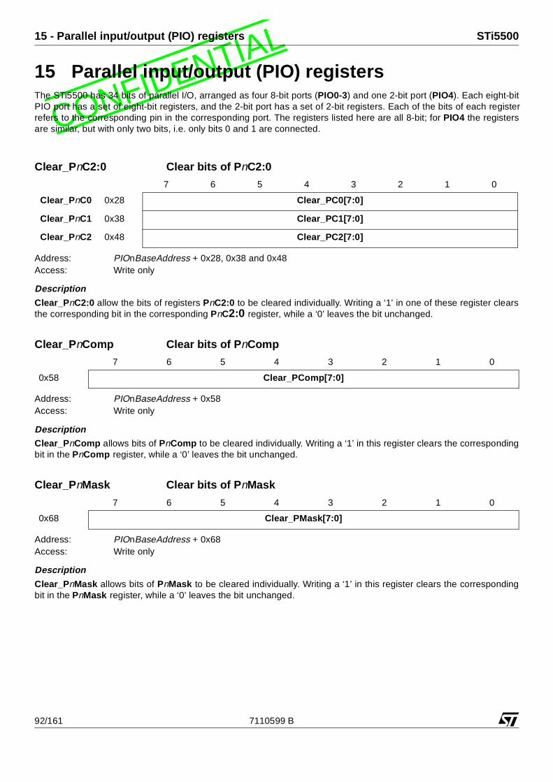
L15 - Parallel input/output (PIO) registers STi5500
CONFIDENTIA15 Parallel input/output (PIO) registersThe STi5500 has 34 bits of parallel I/O, arranged as four 8-bit ports (PIO0-3) and one 2-bit port (PIO4). Each eight-bitPIO port has a set of eight-bit registers, and the 2-bit port has a set of 2-bit registers. Each of the bits of each registerrefers to the corresponding pin in the corresponding port. The registers listed here are all 8-bit; for PIO4 the registersare similar, but with only two bits, i.e. only bits 0 and 1 are connected.
Clear_PnC2:0 Clear bits of PnC2:0
Address: PIOnBaseAddress + 0x28, 0x38 and 0x48Access: Write only
Description
Clear_PnC2:0 allow the bits of registers PnC2:0 to be cleared individually. Writing a ‘1’ in one of these register clearsthe corresponding bit in the corresponding PnC2:0 register, while a ‘0’ leaves the bit unchanged.
Clear_PnComp Clear bits of PnComp
Address: PIOnBaseAddress + 0x58Access: Write only
DescriptionClear_PnComp allows bits of PnComp to be cleared individually. Writing a ‘1’ in this register clears the correspondingbit in the PnComp register, while a ‘0’ leaves the bit unchanged.
Clear_PnMask Clear bits of PnMask
Address: PIOnBaseAddress + 0x68Access: Write only
Description
Clear_PnMask allows bits of PnMask to be cleared individually. Writing a ‘1’ in this register clears the correspondingbit in the PnMask register, while a ‘0’ leaves the bit unchanged.
7 6 5 4 3 2 1 0
Clear_PnC0 0x28 Clear_PC0[7:0]
Clear_PnC1 0x38 Clear_PC1[7:0]
Clear_PnC2 0x48 Clear_PC2[7:0]
7 6 5 4 3 2 1 0
0x58 Clear_PComp[7:0]
7 6 5 4 3 2 1 0
0x68 Clear_PMask[7:0]
92/161 7110599 B

LSTi5500 15 - Parallel input/output (PIO) registers
CONFIDENTIAClear_PnOut Clear bits of PnOut
Address: PIOnBaseAddress + 0x08Access: Write only
Description
Clear_PnOut allows bits of PnOut to be cleared individually. Writing a ‘1’ in this register clears the corresponding bit inthe PnOut register, while a ‘0’ leaves the bit unchanged.
PnC2:0 PIO configuration
Address: PIOnBaseAddress + 0x20, 0x30 and 0x40Access: Read/writeReset state: 0
Description
There are three configuration registers (PnC0, PnC1 and PnC2) for each port, which are used to configure the PIO portpins. Each pin can be configured as an input, output, bidirectional, or alternative function pin (if any), with options forthe output driver configuration. Three bits, one bit from each of the three registers, configure the corresponding bit of the port. The configuration of thecorresponding I/O pin for each valid bit setting is given in Table 15.1.
The PnC registers are each mapped onto two additional addresses Set_PnC and Clear_PnC so that bits can be set orcleared individually.
7 6 5 4 3 2 1 0
0x08 Clear_POut[7:0]
7 6 5 4 3 2 1 0
PnC0 0x20 ConfigData0[7:0]
PnC1 0x30 ConfigData1[7:0]
PnC2 0x40 ConfigData2[7:0]
PnC2[y] PnC1[y] PnC0[y] Bit y configuration Bit y output
0 0 0 Input Hi-Z.
0 0 1 Bidirectional Open drain.
0 1 0 Output Push-pull.
0 1 1 Bidirectional Open drain.
1 0 0 Input Hi-Z.
1 0 1 Input Hi-Z.
1 1 0 Alternative function output Push-pull.
1 1 1 Alternative function bidirectional Open drain.
Table 15.1 PIO bit configuration encoding
7110599 B 93/161

L15 - Parallel input/output (PIO) registers STi5500
CONFIDENTIAPnComp PIO input comparison
Address: PIOnBaseAddress + 0x50Access: Read/writeReset state: 0
DescriptionThe input compare register PnComp can be used to cause an interrupt if the input value differs from a fixed value. The input data from the PIO ports pins will be compared with the value held in PnComp. If any of the input bits is differ-ent from the corresponding bit in the PnComp register and the corresponding bit position in PnMask is set to 1, thenthe internal interrupt signal for the port will be set to 1.The compare function is sensitive to changes in levels on the pins. For the comparison to be seen as a valid interruptby an interrupt handler, the change in state on the input pin must be longer in duration than the interrupt response time.The compare function is operational in all configurations for each PIO bit, including the alternative function modes.The PnOut register is mapped onto two additional addresses Set_PnOut and Clear_PnOut so that bits can be set orcleared individually.
PnIn PIO input
Address: PIOnBaseAddress + 0x10Access: Read onlyReset state: 0
DescriptionThe data read from this register will give the logic level present on the input pins of the port at the start of the read cycleto this register. Each bit reflects the input value of the corresponding bit of the port. The read data will be the last valuewritten to the register regardless of the pin configuration selected.
PnMask PIO input comparison mask
Address: PIOnBaseAddress + 0x60Access: Read/writeReset state: 0
Description
When a bit is set to 1, the compare function for the internal interrupt for the port is enabled for that bit. If the respectivebit (7 to 0) of the input is different from the corresponding bit in the PnComp register, then an interrupt is generated.
The PnMask register is mapped onto two additional addresses Set_PnMask and Clear_PnMask so that bits can beset or cleared individually.
7 6 5 4 3 2 1 0
0x50 PComp[7:0]
7 6 5 4 3 2 1 0
0x10 PIn[7:0]
7 6 5 4 3 2 1 0
0x60 PMask[7:0]
94/161 7110599 B

LSTi5500 15 - Parallel input/output (PIO) registers
CONFIDENTIAPnOut PIO output
Address: PIOnBaseAddress + 0x00Access: Read/writeReset state: 0
DescriptionThis register holds output data for the port. Each bit defines the output value of the corresponding bit of the port. The PnOut register is mapped onto two additional addresses Set_PnOut and Clear_PnOut so that bits can be set orcleared individually.
Set_PnC2:0 Set bits of PnC2:0
Address: PIOnBaseAddress + 0x24, 0x34 and 0x44Access: Write only
DescriptionSet_PnC2:0 allow the bits of registers PnC2:0 to be set individually. Writing a ‘1’ in one of these registers sets the cor-responding bit in the corresponding PnC2:0 register, while a ‘0’ leaves the bit unchanged.
Set_PnComp Set bits of PnComp
Address: PIOnBaseAddress + 0x54Access: Write only
Description
Set_PnComp allows bits of PnComp to be set individually. Writing a ‘1’ in this register sets the corresponding bit in thePnComp register, while a ‘0’ leaves the bit unchanged.
Set_PnMask Set bits of PnMask
Address: PIOnBaseAddress + 0x64Access: Write only
Description
Set_PnMask allows bits of PnMask to be set individually. Writing a ‘1’ in this register sets the corresponding bit in thePnMask register, while a ‘0’ leaves the bit unchanged.
7 6 5 4 3 2 1 0
0x00 POut[7:0]
7 6 5 4 3 2 1 0
Set_PnC0 0x24 Set_PC0[7:0]
Set_PnC1 0x34 Set_PC1[7:0]
Set_PnC2 0x44 Set_PC2[7:0]
7 6 5 4 3 2 1 0
0x54 Set_PComp[7:0]
7 6 5 4 3 2 1 0
0x64 Set_PMask[7:0]
7110599 B 95/161

L15 - Parallel input/output (PIO) registers STi5500
CONFIDENTIASet_PnOut Set bits of PnOut
Address: PIOnBaseAddress + 0x04Access: Write only
Description
Set_PnOut allows bits of PnOut to be set individually. Writing a ‘1’ in this register sets the corresponding bit in thePnOut register, while a ‘0’ leaves the bit unchanged.
7 6 5 4 3 2 1 0
0x04 Set_POut[7:0]
96/161 7110599 B
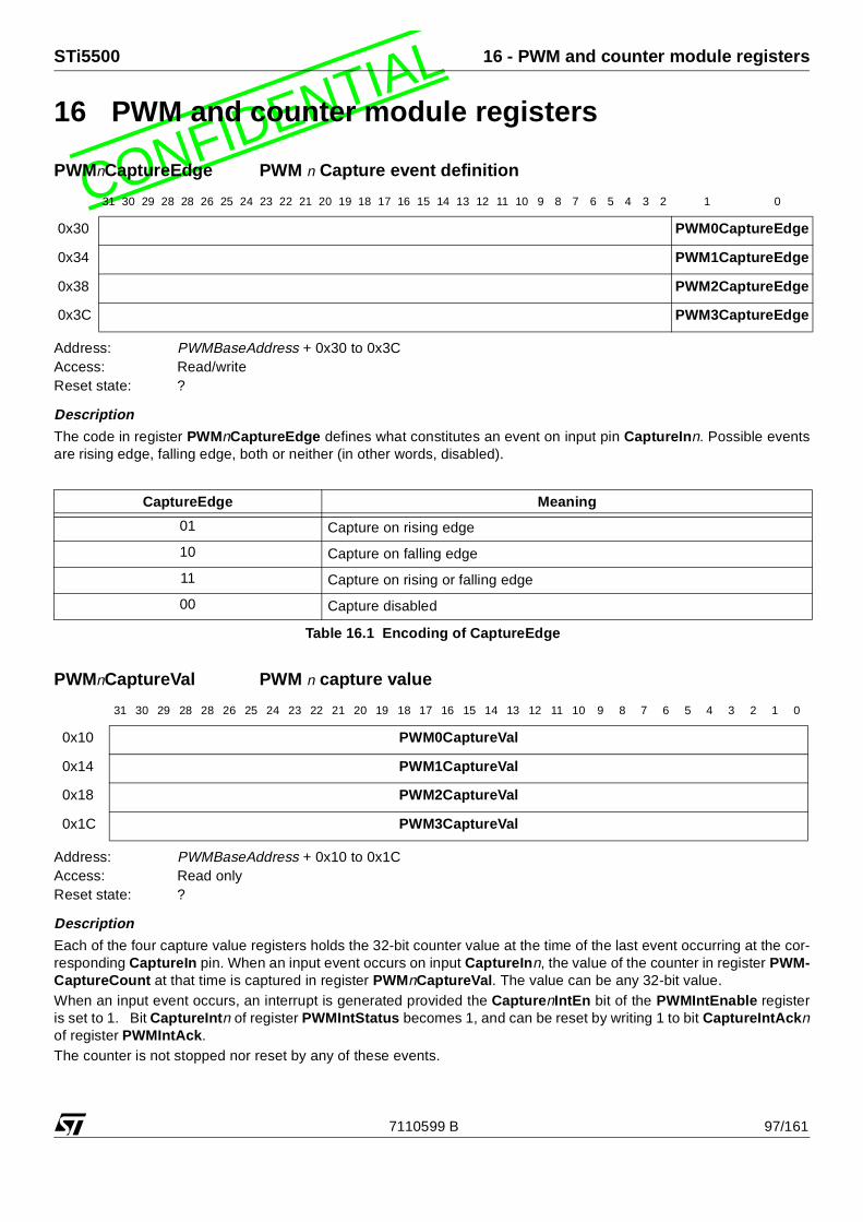
LSTi5500 16 - PWM and counter module registers
CONFIDENTIA16 PWM and counter module registers
PWMnCaptureEdge PWM n Capture event definition
Address: PWMBaseAddress + 0x30 to 0x3CAccess: Read/writeReset state: ?
Description
The code in register PWMnCaptureEdge defines what constitutes an event on input pin CaptureInn. Possible eventsare rising edge, falling edge, both or neither (in other words, disabled).
PWMnCaptureVal PWM n capture value
Address: PWMBaseAddress + 0x10 to 0x1CAccess: Read onlyReset state: ?
Description
Each of the four capture value registers holds the 32-bit counter value at the time of the last event occurring at the cor-responding CaptureIn pin. When an input event occurs on input CaptureInn, the value of the counter in register PWM-CaptureCount at that time is captured in register PWMnCaptureVal. The value can be any 32-bit value.When an input event occurs, an interrupt is generated provided the CapturenIntEn bit of the PWMIntEnable registeris set to 1. Bit CaptureIntn of register PWMIntStatus becomes 1, and can be reset by writing 1 to bit CaptureIntAcknof register PWMIntAck.The counter is not stopped nor reset by any of these events.
31 30 29 28 28 26 25 24 23 22 21 20 19 18 17 16 15 14 13 12 11 10 9 8 7 6 5 4 3 2 1 0
0x30 PWM0CaptureEdge
0x34 PWM1CaptureEdge
0x38 PWM2CaptureEdge
0x3C PWM3CaptureEdge
CaptureEdge Meaning
01 Capture on rising edge
10 Capture on falling edge
11 Capture on rising or falling edge
00 Capture disabled
Table 16.1 Encoding of CaptureEdge
31 30 29 28 28 26 25 24 23 22 21 20 19 18 17 16 15 14 13 12 11 10 9 8 7 6 5 4 3 2 1 0
0x10 PWM0CaptureVal
0x14 PWM1CaptureVal
0x18 PWM2CaptureVal
0x1C PWM3CaptureVal
7110599 B 97/161

L16 - PWM and counter module registers STi5500
CONFIDENTIAPWMnCompareOutVal PWM n compare output value
Address: PWMBaseAddress + 0x40 to 0x4CAccess: Read/writeReset state: ?
DescriptionRegister PWMCompareOutValN holds the value which will be written to the PWMCompareOutN pin when thecompare value in PWMCompareValN matches the counter value PWMCaptureCount.
PWMnCompareVal PWM n compare value
Address: PWMBaseAddress + 0x20 to 0x2CAccess: Read/writeReset state: ?
Description
Each of the four compare registers PWMnCompareVal in the module can be set to any 32-bit value. When the counterin register PWMCaptureCount reaches the value of register PWMnCompareVal, two things happen:
1 An interrupt is generated provided the PWMnCompareIntEn bit of the PWMIntEnable register is set to 1. BitPWMCompareIntN of register PWMIntStatus becomes 1, and can be reset by writing 1 to bit PWMnCompareIn-tAck of register PWMIntAck.
2 Pin PWMnCompareOut takes on the value set in register PWMnCompareOutVal.The counter is not stopped nor reset by any of these events.
31 30 29 28 28 26 25 24 23 22 21 20 19 18 17 16 15 14 13 12 11 10 9 8 7 6 5 4 3 2 1 0
0x40CompareOutVal0
0x44CompareOutVal1
0x48CompareOutVal2
0x4CCompareOutVal3
31 30 29 28 28 26 25 24 23 22 21 20 19 18 17 16 15 14 13 12 11 10 9 8 7 6 5 4 3 2 1 0
0x20 PWM0CompareVal
0x24 PWM1CompareVal
0x28 PWM2CompareVal
0x2C PWM3CompareVal
98/161 7110599 B

LSTi5500 16 - PWM and counter module registers
CONFIDENTIAPWMnVal PWM n pulse width
Address: PWMBaseAddress + 0x00 to 0x0CAccess: Read/writeReset state: ?
Description
These registers hold the counter values, which are used to determine the width of the pulse generated on the PWMOutpin.
PWMOut pulse width = (PWMVal + 1) x prescaled clock period
If PWMVal is 255 then PWMOut does not go low.
Comment: Should this say 9-bit? Or is the diagram wrong? TP2 says 8-bit 7:0. TP3 says 8-bit 8:0
PWMCaptureCount PWM capture/compare counter
Address: PWMBaseAddress + 0x64Access: Read/writeReset state: ?
DescriptionThis register holds the shared capture/compare counter used by all the capture and compare functions.The capture/compare counter is clocked from the prescaled system clock. The prescaling factor, and therefore theperiod represented by one count, is determined by the value of field CaptureClkValue in register PWMControl. Thefactor can be from 1 to 32.The counter is enabled by setting the PWMCaptureEnable bit of the PWMControl register to 1. When it is disabled(PWMCaptureEnable is 0), none of the capture or compare functions work. PWMCaptureCount can be read or writ-ten at any time.When the capture/compare counter reaches its maximum count of #FFFFFFFF, it wraps round to count up from zeroagain.
PWMControl PWM control register
Address: PWMBaseAddress + 0x50Access: Read/writeReset state: ?
31 30 29 28 28 26 25 24 23 22 21 20 19 18 17 16 15 14 13 12 11 10 9 8 7 6 5 4 3 2 1 0
0x00 PWM0Val
0x04 PWM1Val
0x08 PWM2Val
0x0C PWM3Val
31 30 29 28 28 26 25 24 23 22 21 20 19 18 17 16 15 14 13 12 11 10 9 8 7 6 5 4 3 2 1 0
0x64 CaptureCount
31 30 29 28 28 26 25 24 23 22 21 20 19 18 17 16 15 14 13 12 11 10 9 8 7 6 5 4 3 2 1 0
0x50CaptureEnable
PWMEnable
CaptureClkValue
PWMClkValue
7110599 B 99/161

L16 - PWM and counter module registers STi5500
CONFIDENTIADescription
PWMCount PWM output counter
Address: PWMBaseAddress + 0x60Access: Read/write (but see text)Reset state: ?
Description
PWM output counter. The counter (in register PWMCount) is enabled by setting the PWMEnable bit of the PWMCon-trol register to 1. When it is disabled (PWMEnable is 0), pin PWMOut is forced low. PWMCount is writable at any timebut can have a synchronization latency.
PWMIntAck PWM interrupt acknowledge
Address: PWMBaseAddress + 0x5CAccess: Write only
Description
Bit Bit field Function
10 CaptureEnable Enables capture/compare counter when = 1
9 PWMEnable Enables PWM counter when = 1
8:4 CaptureClkValue Capture/compare clock prescale factor 0-31 (divide clock by value + 1)
3:0 PWMClkValue PWM clock prescale factor 0-15 (divide clock by value + 1)
31 30 29 28 28 26 25 24 23 22 21 20 19 18 17 16 15 14 13 12 11 10 9 8 7 6 5 4 3 2 1 0
0x60 Count
31 30 29 28 28 26 25 24 23 22 21 20 19 18 17 16 15 14 13 12 11 10 9 8 7 6 5 4 3 2 1 0
0x5CC
mp
IA3
Cm
pIA
2
Cm
pIA
1
Cm
pIA
0
Cp
tIA
3
Cp
tIA
2
Cp
tIA
1
Cp
tIA
0
IntA
ckBit Bit field Function
8 CmpIA3 CompareIntAck3 Compare 3 interrupt acknowledge: write 1 to reset status bit
7 CmpIA2 CompareIntAck2 Compare 2 interrupt acknowledge: write 1 to reset status bit
6 CmpIA1 CompareIntAck1 Compare 1 interrupt acknowledge: write 1 to reset status bit
5 CmpIA0 CompareIntAck0 Compare 0 interrupt acknowledge: write 1 to reset status bit
4 CptIA3 CaptureIntAck3 Capture 3 interrupt acknowledge: write 1 to reset status bit
3 CptIA2 CaptureIntAck2 Capture 2 interrupt acknowledge: write 1 to reset status bit
2 CptIA1 CaptureIntAck1 Capture 1 interrupt acknowledge: write 1 to reset status bit
1 CptIA0 CaptureIntAck0 Capture 0 interrupt acknowledge: write 1 to reset status bit.
0 IntAck PWMIntAck Interrupt acknowledge: write 1 to reset PWMInt to 0
100/161 7110599 B

LSTi5500 16 - PWM and counter module registers
CONFIDENTIAPWMIntEnable PWM interrupt enable
Address: PWMBaseAddress + 0x54Access: Read/writeReset state:
Description
PWMIntStatus PWM interrupt status
Address: PWMBaseAddress + 0x58Access: Read onlyReset state:
31 30 29 28 28 26 25 24 23 22 21 20 19 18 17 16 15 14 13 12 11 10 9 8 7 6 5 4 3 2 1 0
0x54
Cm
pIE
3
Cm
pIE
2
Cm
pIE
1
Cm
pIE
0
Cp
tIE
3
Cp
tIE
2
Cp
tIE
1
Cp
tIE
0
IntE
n
Bit Bit field Function
8 CmpIE3 CompareIntEn3 Compare 3 interrupt enable: 1 = enabled
7 CmpIE2 CompareIntEn2 Compare 2 interrupt enable: 1 = enabled
6 CmpIE1 CompareIntEn1 Compare 1 interrupt enable: 1 = enabled
5 CmpIE0 CompareIntEn0 Compare 0 interrupt enable: 1 = enabled
4 CptIE3 CaptureIntEn3 Capture 3 interrupt enable: 1 = enabled
3 CptIE2 CaptureIntEn2 Capture 2 interrupt enable: 1 = enabled
2 CptIE1 CaptureIntEn1 Capture 1 interrupt enable: 1 = enabled
1 CptIE0 CaptureIntEn0 Capture 0 interrupt enable: 1 = enabled
0 IntEn PWMIntEn PWM counter overflow interrupt enable
31 30 29 28 28 26 25 24 23 22 21 20 19 18 17 16 15 14 13 12 11 10 9 8 7 6 5 4 3 2 1 0
0x58
Cm
p3
Cm
p2
Cm
p1
Cm
p0
Cp
t3
Cp
t2
Cp
t1
Cp
t0
Int
7110599 B 101/161
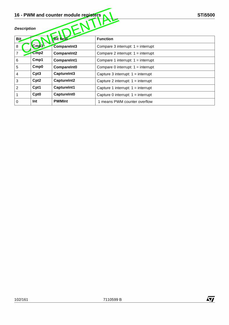
L16 - PWM and counter module registers STi5500
CONFIDENTIADescription
Bit Bit field Function
8 Cmp3 CompareInt3 Compare 3 interrupt: 1 = interrupt
7 Cmp2 CompareInt2 Compare 2 interrupt: 1 = interrupt
6 Cmp1 CompareInt1 Compare 1 interrupt: 1 = interrupt
5 Cmp0 CompareInt0 Compare 0 interrupt: 1 = interrupt
4 Cpt3 CaptureInt3 Capture 3 interrupt: 1 = interrupt
3 Cpt2 CaptureInt2 Capture 2 interrupt: 1 = interrupt
2 Cpt1 CaptureInt1 Capture 1 interrupt: 1 = interrupt
1 Cpt0 CaptureInt0 Capture 0 interrupt: 1 = interrupt
0 Int PWMInt 1 means PWM counter overflow
102/161 7110599 B

LSTi5500 17 - SmartCard interface (Sc) registers
CONFIDENTIA17 SmartCard interface (Sc) registers
ScnClkCon SmartCard n clock control
Address: SmartCardnBaseAddress + 0x04Access: Write onlyReset state: 0
Description
The ScnClkCon register controls the source of the clock and determines whether the SmartCard clock output isenabled. The programmable divider and the output are reset when the enable bit is set to 0.
ScnClkVal SmartCard n clock
Address: SmartCardnBaseAddress + 0x00Access: Write onlyReset state: 0
Comment: ...but 0 is an illegal value!
DescriptionThe ScnClkVal register determines the SmartCard clock frequency. The 5-bit value given in the register is multiplied by2 to give the division factor of the input clock frequency. For example, if ScnSlkVal is 8 then the input clock frequencyis divided by 16. The value zero must not be written into this register.The divider is updated with the new value for the divider ratio on the next rising or falling edge of the output clock.
31 30 29 28 28 26 25 24 23 22 21 20 19 18 17 16 15 14 13 12 11 10 9 8 7 6 5 4 3 2 1 0
0x04 Enable Source
Bit Bit field Function
7:2 Reserved. Write 0.
1 EnableSmartCard clock generator enable bit.
0 Stop clock, set output low and reset divider.1 Enable clock generator.
0 SourceSelects source of SmartCard clock.
0 Selects global clock.1 Selects external pin.
31 30 29 28 28 26 25 24 23 22 21 20 19 18 17 16 15 14 13 12 11 10 9 8 7 6 5 4 3 2 1 0
0x00 ScClkVal
7110599 B 103/161

L18 - Sub-picture decoder (SPD) registers STi5500
CONFIDENTIA18 Sub-picture decoder (SPD) registers
SPD_CTL1 Control Register 1
Address: SubPictureBaseAddress + 0x00Access: Read/writeReset state: 0Synchronization: VSYNC (field)
DescriptionThis register contains control bits for the subpicture decoder.
SPD_CTL2 Control Register 2
Address: SubPictureBaseAddress + 0x02Access: Read/writeReset state: 0Synchronization: None
Description
This register contains control bits for the subpicture decoder.Ri Reset Input Fifo. This bit, when set, resets the bit-buffer input FIFO.Rc Reset Lut #2. This bit, when set, resets the auto-increment address counter.
7 6 5 4 3 2 1 0
0x00 SPP B H V D S
Field Bit Description
SPP 5Sub-picture pause mode. When this bit is set the 90 KHz clock in the sub-picture decoder is paused.
B 4 Bypass. This bit when set puts the run-length decoder into transparent mode. This allowsstandard 2-bit-per-pixel bitmaps to be fed into the sub-picture decoder.
H 3 Highlight Enable. This bit, when set, turns on highlighting inside the sub-picture display area.
V 2Display Active. This bit, when reset, turns off the sub-picture display, however, decoding stillgoes on even when the display is disabled. When decoding is disabled using the ‘Decoderactive’ bit then the display is automatically disabled.
D 1Decoder Active. This bit is set by the decoder when, at shadow register update, the Sub-picture start bit is sampled high. When the decoder active bit is reset decoding is disabledand can only be re-enabled by the decoder start bit.
S 0Sub-Picture Decoder Start command. When this bit is set it indicates the start of a newsubpicture unit. The subpicture decoder will then reset the local time reference counter. Thestate is sampled on each VSYNC.
Table 18.1 Register fields
7 1 0
0x02 Ri Rc
104/161 7110599 B

LSTi5500 18 - Sub-picture decoder (SPD) registers
CONFIDENTIASPD_HLRC Highlight Region Contrast
Address: SubPictureBaseAddress + 0x16 and 0x17Access: Read/writeReset state: 0Synchronization: VSYNC
Description
These registers contain the highlight contrast map values.
SPD_HLRCO Highlight Region Color
Address: SubPictureBaseAddress + 0x14 and 0x15Access: Read/writeReset state: 0Synchronization: VSYNC
DescriptionThese registers contain the highlight color map values.
SPD_HLEX Highlight Region End X
Address: SubPictureBaseAddress + 0x10 and 0x11Access: Read/writeReset state: 0Synchronization: VSYNC
DescriptionHighlight region end position X-coordinate.
SPD_HLEY Highlight Region End Y
7 4 3 0
0x16 e2[3:0] e1[3:0]
0x17 p[3:0] b[3:0]
7 4 3 0
0x14 e2[3:0] e1[3:0]
0x15 p[3:0] b[3:0]
7 2 1 0
0x10 SPD_HLEX[9:8]
0x11 SPD_HLEX[7:0]
7 2 1 0
0x12 SPD_HLEY[9:8]
0x13 SPD_HLEY[7:0]
7110599 B 105/161

L18 - Sub-picture decoder (SPD) registers STi5500
CONFIDENTIAAddress: SubPictureBaseAddress + 0x12 and 0x13Access: Read/writeReset state: 0Synchronization: VSYNC
Description
Highlight region end position Y-coordinate.
SPD_HLSX Highlight Region Start X
Address: SubPictureBaseAddress + 0x0C and 0x0DAccess: Read/writeReset state: 0Synchronization: VSYNC
Description
Highlight region start position X-coordinate.
SPD_HLSY Highlight Region Start Y
Address: SubPictureBaseAddress + 0x0E and 0x0FAccess: Read/writeReset state: 0Synchronization: VSYNC
DescriptionHighlight region start position Y-coordinate.
SPD_LUT Main Lookup Table
Address: SubPictureBaseAddress + 0x03Access: Read/writeReset state: 0Synchronization: None
Description
This register allows input of the main lookup table. Writing to this register auto-increments the address in the lookuptable. For each color, starting with color 0, the Y component (8-bit) is written first followed by U and V. The process con-tinues for each color up to 16 colors.
7 2 0
0x0C SPD_HLSX[9:8]
0x0D SPD_HLSX[7:0]
7 6 5 4 3 2 1 0
0x0E SPD_HLSY[9:8]
0x0F SPD_HLSY[7:0]
7 0
0x03 SPD_LUT[7:0]
106/161 7110599 B

LSTi5500 18 - Sub-picture decoder (SPD) registers
CONFIDENTIASPD_RST Sub-picture reset
Address: SubPictureBaseAddress + 0x01Access: Read/writeReset state: 0Synchronization: Edge triggered
DescriptionThis register contains the subpicture reset, SPR. When this bit is set to ’1’ the subpicture decoder is reset. ( The sub-picture decoder is also reset by a hard reset.)
SPD_SPB Sub-picture buffer begin
Address: SubPictureBaseAddress + 0x50 and 0x51Access: Read/writeReset state: 0Synchronization: None
DescriptionThis register gives the start address of the sub-picture circular buffer as an offset from the base of SDRAM in units of64 bytes. The buffer should be aligned on a 1 Kbyte boundary.
SPD_SPE Sub-picture buffer end
Address: SubPictureBaseAddress + 0x52 and 0x53Access: Read/writeReset state: 0Synchronization: None
Description
This register holds the stop address of the sub-picture circular buffer as an offset from the base of SDRAM in units of64bytes. The buffer should be aligned on a 1 Kbyte boundary.
7 1 0
0x01 SPR
7 6 5 4 3 2 1 0
0x50 SPD_SPB[10:8]
0x51 SPD_SPB[7:0]
7 6 5 4 3 2 1 0
0x52 SPD_SPE[10:8]
0x53 SPD_SPE[7:0]
7110599 B 107/161

L18 - Sub-picture decoder (SPD) registers STi5500
CONFIDENTIASPD_SPRead SubPicture Read Pointer
Address: SubPictureBaseAddress + 0x4EAccess: Read/writeReset state: 0Synchronization: VSYNC
Description
These three registers are accessed serially. The byte pointer is reset by a hardware reset. This register is used whenthe software needs to set the read address of the sub-picture decoder and is programmed in units of 64-bit words. Thisvalue is taken into account after a VSYNC. This register holds the absolute address in the memory.
SPD_SPWrite SubPicture Write Pointer
Address: SubPictureBaseAddress + 0x4FAccess: Read/writeReset state: 0Synchronization: None
DescriptionThese three registers are accessed serially. The byte pointer is reset by a hardware reset. This register is used whenthe software needs to set the write address of the sub-picture decoder and is programmed in units of 64-bit words. It isrecommended to stop loading Sub-picture data to the sub-picture decoder FIFO before changing the value of this reg-ister. This register holds the absolute address in the memory.
SPD_SXD0 Sub-picture display area
Address: SubPictureBaseAddress + 0x24 and 0x25Access: Read/writeReset state: 0Synchronization: VSYNC
Description
These registers contain the parameters which define the subpicture display area within the subpicture decode area.The value represents an offset from the corresponding parameter used to define the subpicture decode area.For example: The true horizontal start position of the subpicture display will be equal to XDO + SXDO.
7 2 0
1st cycle SPD_SPRead[18:16]
2nd cycle SPD_SPRead[15:8]
3rd cycle SPD_SPRead[7:0]
7 2 0
1st cycle SPD_SPWrite[18:16]
2nd cycle SPD_SPWrite[15:8]
3rd cycle SPD_SPWrite[7:0]
7 6 5 4 3 2 1 0
0x24 SPD_SXD0[9:8]
0x25 SPD_SXD0[7:0]
108/161 7110599 B

LSTi5500 18 - Sub-picture decoder (SPD) registers
CONFIDENTIASPD_SXD1 Subpicture Display Area
Address: SubPictureBaseAddress + 0x28 and 0x29Access: Read/writeReset state: 0Synchronization: VSYNC
Description
These registers contain the parameters which define the subpicture display area within the subpicture decode area.The value represents an offset from the corresponding parameter used to define the subpicture decode area.
SPD_SYD0 Subpicture Display Area
Address: SubPictureBaseAddress + 0x26 and 0x27Access: Read/writeReset state: 0Synchronization: VSYNC
DescriptionThese registers contain the parameters which define the subpicture display area within the subpicture decode area.The value represents an offset from the corresponding parameter used to define the subpicture decode area.
SPD_SYD1 Subpicture Display Area
Address: SubPictureBaseAddress + 0x2A and 0x2BAccess: Read/writeReset state: 0Synchronization: VSYNC
Description
These registers contain the parameters which define the subpicture display area within the subpicture decode area.The value represents an offset from the corresponding parameter used to define the subpicture decode area.
7 6 5 4 3 2 1 0
0x28 SPD_SXD1[9:8]
0x29 SPD_SXD1[7:0]
7 6 5 4 3 2 1 0
0x26 SPD_SYD0[9:8]
0x27 SPD_SYD0[7:0]
7 6 5 4 3 2 1 0
0x2A SPD_SYD1[9:8]
0x2B SPD_SYD1[7:0]
7110599 B 109/161

L18 - Sub-picture decoder (SPD) registers STi5500
CONFIDENTIASPD_XD0 Sub-picture X Offset
Address: SubPictureBaseAddress + 0x04 and 0x05Access: Read/writeReset state: 0Synchronization: VSYNC
Description
This register value sets the horizontal position of the left hand side of the active subpicture decode region. The positionis measured in number of pixels from the left hand edge of the screen.
SPD_XD1 Horizontal Position of Active Area
Address: SubPictureBaseAddress + 0x08 and 0x09Access: Read/writeReset state: 0Synchronization: VSYNC
DescriptionThis register value sets the horizontal position of the right side of the active subpicture decode region. The position ismeasured in units of pixels from the left hand edge of the screen.
SPD_YD0 Sub-picture Y Offset
Address: SubPictureBaseAddress + 0x06 and 0x07Access: Read/writeReset state: 0Synchronization: VSYNC
Description
This register value sets the vertical position of the top of the active subpicture decode region. The position is measuredin number of pixels from the top edge of the screen.
7 6 5 4 3 2 1 0
0x04 SPD_XD0[9:8]
0x05 SPD_XD0[7:0]
7 6 5 4 3 2 1 0
0x08 SPD_XD1[9:8]
0x09 SPD_XD1[7:0]
7 6 5 4 3 2 1 0
0x06 SPD_YD0[9:8]
0x07 SPD_YD0[7:0]
110/161 7110599 B

LSTi5500 18 - Sub-picture decoder (SPD) registers
CONFIDENTIASPD_YD1 Vertical Position of Active Area
Address: SubPictureBaseAddress + 0x0A and 0x0BAccess: Read/writeReset state: 0Synchronization: VSYNC
Description
This register value sets the vertical position of the bottom of the active subpicture decode region. The position is mea-sured in units of pixels from the top edge of the screen.
7 6 5 4 3 2 1 0
0x0A SPD_YD1[9:8]
0x0B SPD_YD1[7:0]
7110599 B 111/161

L19 - Synchronous serial controller (SSC) registers STi5500
CONFIDENTIA19 Synchronous serial controller (SSC) registers
SSC0BRG SSC 0 baud rate generation
Address: SSC0BaseAddress + 0x00Access: Read/writeReset state: 1
DescriptionThis address is dual purpose. When reading, the current 16-bit counter value is returned. When a value is to thisaddress, the 16-bit reload register is loaded with that value.
SSC0Con SSC 0 control
Address: SSC0BaseAddress + 0x0CAccess: Read/writeReset state: 0
15 14 13 12 11 10 9 8 7 6 5 4 3 2 1 0
0x00 BRG
15 14 13 12 11 10 9 8 7 6 5 4 3 2 1 0
0x0C LPB EN MS SR PO PH HB BM
112/161 7110599 B

LSTi5500 19 - Synchronous serial controller (SSC) registers
CONFIDENTIADescription
Comment: Reset value for BM is illegal.
SSC0IEn SSC 0 interrupt enable
Address: SSC0BaseAddress + 0x10Access: Read/writeReset state: 0
Bit Bit Field Reset State Function
15:11 Reserved
10 LPB 0SSC Loopback Bit
0 disabled1 shift register output is connected to shift register input
9 EN 0SSC Enable Bit
0 transmission and reception disabled1 transmission and reception enabled
8 MS 0SSC Master Select Bit
0 slave mode1 master mode
7 SRSSC Software Reset
0 device is not reset1 all functions are reset while this bit is set
6 PO 0SSC Clock Polarity Control Bit
0 clock idles at logic 01 clock idles at logic 1
5 PH 0SSC Clock Phase Control Bit
0 pulse in second half cycle1 pulse in first half cycle
4 HB 0SSC Heading Control Bit
0 LSB first1 MSB first
3:0 BM 0000
SSC Data Width Selection
BM[3:0] Data Width0000 Reserved. Do not use this combination.0001 2 bits0010 3 bits ... ...1111 16 bits
15 14 13 12 11 10 9 8 7 6 5 4 3 2 1 0
0x10
AR
BL
EN
ST
OP
EN
AA
SE
N
PE
EN
RE
EN
TE
EN
TIE
N
RIE
N
7110599 B 113/161

L19 - Synchronous serial controller (SSC) registers STi5500
CONFIDENTIADescriptionThis register holds the interrupt enable bits, which can be used to mask the interrupts.
SSC0RBuf SSC 0 receive buffer
Address: SSC0BaseAddress + 0x08Access: Read onlyReset state: 0
Description
Receive buffer data D15 to D0.
SSC0SlAd SSC 0 slave address
Address: SSC0BaseAddress + 0x1CAccess: Write onlyReset state: 0
Bit Bit Field Reset State Function
15:9 Reserved
8 ARBLEN 0 I2C Arbitration Lost Interrupt Enable
1 arbitration lost interrupt enabled
7 STOPEN 0 I2C Stop Condition Interrupt Enable
1 stop condition interrupt enabled
6 AASEN 0 I2C Addressed As Slave Interrupt Enable
1 addressed as slave interrupt enabled
5 Reserved
4 PEEN 0Phase Error Interrupt Enable
1 phase error interrupt enabled
3 REEN 0Receive Error Interrupt Enable
1 receive error interrupt enabled
2 TEEN 0Transmit Error Interrupt Enable
1 transmit error interrupt enabled
1 TIEN 0Transmitter Buffer Empty Interrupt Enable
1 transmitter buffer empty interrupt enabled
0 RIEN 0Receiver Buffer Full Interrupt Enable
1 receiver buffer interrupt enabled
15 14 13 12 11 10 9 8 7 6 5 4 3 2 1 0
0x08 RD[15:0]
15 14 13 12 11 10 9 8 7 6 5 4 3 2 1 0
0x1C SL[9:7] SL[6:0]
114/161 7110599 B

LSTi5500 19 - Synchronous serial controller (SSC) registers
CONFIDENTIADescriptionThe slave address is written into this register. If the address is a 10-bit address it is written into bits 9:0. If the addressis a 7-bit address then it is written into bits 6:0.
SSC0Stat SSC 0 status
Address: SSC0BaseAddress + 0x14Access: Read onlyReset state: 2, i.e. all active bits clear except TIR.
Description
SSC0TBuf SSC 0 transmit buffer
Address: SSC0BaseAddress + 0x04Access: Write only
15 14 13 12 11 10 9 8 7 6 5 4 3 2 1 0
0x14 BUSY ARBL STOP AAS CLST PE RE TE TIR RIR
Bit Bit Field Reset State Function
15:10 Reserved
9 BUSY 0 I2C bus busy flag
1 I2C bus busy
8 ARBL 0 I2C arbitration lost flag
1 arbitration lost
7 STOP 0 I2C stop condition flag
1 stop condition detected
6 AAS 0 I2C addressed as slave flag
1 addressed as slave device
5 CLSTI2C clock stretch flag
1clock stretching in operation
4 PE 0Phase error flag
1 phase error set
3 RE 0Receive error flag
1 receive error set
2 TE 0Transmit error flag
1transmit error set
1 TIR 1Transmitter buffer empty flag
1transmitter buffer empty
0 RIR 0Receiver buffer full flag
1receiver buffer full
15 14 13 12 11 10 9 8 7 6 5 4 3 2 1 0
0x04 TD[15:0]
7110599 B 115/161

L19 - Synchronous serial controller (SSC) registers STi5500
CONFIDENTIAReset state: 0
DescriptionTransmit buffer data D15 to D0.
116/161 7110599 B

LSTi5500 20 - Transport stream demultiplexor registers
CONFIDENTIA20 Transport stream demultiplexor registers
STREAM n configuration1stream_conf_1n @ 0x2002580+4n
STREAM n configuration2stream_conf_2n @ 0x2002600+4n
STREAM n configuration3stream_conf_3n @ 0x2002680+4n
A_PTS_REG Audio time stamp
Address: TransportDemuxBaseAddress + 0xFA4Access: Read only
Description
AF_REG1-0 Adaptation field
Address: TransportDemuxBaseAddress + 0xF98 - 0xF9CAccess: Read only
Description
Table 20.2 defines the AF_REG registers, which hold the first eight bytes of the adaptation field. The interrupt is gener-ated if mask = 1.
31 30 29 28 27 26 25 24 23 22 21 20 19 18 17 16 15 14 13 12 11 10 9 8 7 6 5 4 3 2 1 0
0xFA4 A_PTS
Bit Signal Name Comment Type
31:0 A_PTS Actual audio PTS (90 kHz) R
Table 20.1 Contents of register A_PTS_REG
31 30 29 28 27 26 25 24 23 22 21 20 19 18 17 16 15 14 13 12 11 10 9 8 7 6 5 4 3 2 1 0
0xF9C AF_7 AF_6 AF_5 AF_4
0xF98 AF_3 AF_2 AF_1 AF_0
7110599 B 117/161

L20 - Transport stream demultiplexor registers STi5500
CONFIDENTIA
AR_SIZE_REG AR size
Address: TransportDemuxBaseAddress + 0xFB0Access: Read/writeReset state: 0x3E
Description
EN_LINK_REG Enable link
Address: TransportDemuxBaseAddress + 0xFC0Access: Read/writeReset state: 0
Description
Register Address Bit Signal Name Comment Type
AF_REG1 0xF9C
31:24 AF_7 AF Byte #7 R
23:16 AF_6 AF Byte #6 R
15:8 AF_5 AF Byte #5 R
7:0 AF_4 AF Byte #4 R
AF_REG0 0xF98
31:24 AF_3 AF Byte #3 R
23:16 AF_2 AF Byte #2 R
15:8 AF_1 AF Byte #1 R
7:0 AF_0 AF Byte #0 R
Table 20.2 Contents of registers AF_REG[1:0]
31 30 29 28 27 26 25 24 23 22 21 20 19 18 17 16 15 14 13 12 11 10 9 8 7 6 5 4 3 2 1 0
0xFB0 AR_SIZE
Bit Signal Name Comment Type Reset
31:6 Not used
5:0 AR_SIZE Programmable AR size. R/W 0x3E
Table 20.3 Contents of register AR_SIZE_REG
31 30 29 28 27 26 25 24 23 22 21 20 19 18 17 16 15 14 13 12 11 10 9 8 7 6 5 4 3 2 1 0
0xFC0 EL
Bit Field Signal Name Comment Type Res
31:1 Not used
0:0 EL ENABLE_LINK Enable Transport Stream Demultiplexor R/W 0
Table 20.4 Contents of register EN_LINK_REG
118/161 7110599 B

LSTi5500 20 - Transport stream demultiplexor registers
CONFIDENTIAEXTRA_BITS_REG Extra bits
Address: TransportDemuxBaseAddress + 0xFC8Access: Read/writeReset state: Undefined except bit 0 reset to 0.
Description
LINK_STAT_FIFO FIFO status
Address: TransportDemuxBaseAddress + 0xF84Access: Read only
DescriptionThe LINK_STAT_FIFO register is the FIFO status word. For DVB, if bit AF is 1 then LINK_STAT_FIFO(15:0) is set tothe first 2 bytes of the AF. For bit EOS, the delay between the Interrupt generation and the actual transfer of the lastbyte of the section to memory can be up to 4 µs.
31 30 29 28 27 26 25 24 23 22 21 20 19 18 17 16 15 14 13 12 11 10 9 8 7 6 5 4 3 2 1 0
0xFC8 EBI EBI
EB
M
Bit Field Signal Name Comment Type Res
31:13 Not used
12:5 EBI EXTRA_BITS_INPUTIncoming EXTRA_BYTESPlayback rate control
R X
4:1 EBI EXTRA_BITS_INPUTIncoming EXTRA_BYTESCopy guard information
R X
0 EBM EXTRA_BITS_IRQ_MASKInterrupt mask for the extra bits1 Enable interrupt on change of extra bits0 Disable interrupt
R/W 0
Table 20.5 Contents of register EXTRA_BITS_REG
31 30 29 28 27 26 25 24 23 22 21 20 19 18 17 16 15 14 13 12 11 10 9 8 7 6 5 4 3 2 1 0
0xF84
EO
F
EO
S
IF AF
AO
DO
BS
SU
SO
PC
R SN CC PTO
M TM
Bits Field Full field name Meaning Type
31 EOF END_OF_FILTER 1 End of section filtering R
30 EOS END_OF_SECTION 1 End of section transfer R
29 IF INCOMPLETE_FILTER 1 Filtering not complete at end of pack R
28 AF AF 1 Adaptation field received R
27 AO AR_OVERFLOW 1 Acquisition RAM overflow R
26 DO BUF_OVERFLOW 1 Storage buffer overflow R
25 BS BAD_SEC 1 Bad section received R
Table 20.6 Contents of register LINK_STAT_FIFO
7110599 B 119/161

L20 - Transport stream demultiplexor registers STi5500
CONFIDENTIA24 SU SDAV_UNDERFLOW
1 SDAV Underflow if SDAV_overflow = 0
Else interrupt for EXTRA_BITSR
23 SO SDAV_OVERFLOW1 SDAV overflow if SDAV_underflow = 0
Else interrupt for EXTRA_BITSR
22 PCR PCR 1 PCR has been latched R
21 Not used
20:16 SN STREAM_NUMBER Stream number of packet R
15:12 CC Continuity counter Continuity counter R
11:9 PT Packet type
If DVB: Bit 11 PAYLOAD_UNIT_START_INDICATORBit 10 SCRAMBLING_INDICATORBit 9 KEY_INDICATOR (0: even; 1: odd)
If DSS:Bit 11 HD(3)Bit 10 HD(2)Bit 9 KEY_INDICATOR (0: odd; 1: even)
R
8 OM OTHER_MATCH At least 1 match in the top 24 targets R
7:0 TM TARGET_MATCH Shows the 8 lowest target matches R
Bits Field Full field name Meaning Type
Table 20.6 Contents of register LINK_STAT_FIFO
120/161 7110599 B

LSTi5500 20 - Transport stream demultiplexor registers
CONFIDENTIALINK_STAT_REG Status
Address: TransportDemuxBaseAddress + 0xF80Access: Read only except bit 2, which is read/writeReset state: Undefined except bit 2, which is reset to 0
Description
LINK_STAT_REG is the status register.
MODE_REG Mode
Address: TransportDemuxBaseAddress + 0xF90Access: Read/writeReset state: 0x001
DescriptionTable 20.8 defines the mode register. DVB_MODE, DSS_MODE and DVD_MODE are mutually exclusive, so exactlyone of them must be set to 1.
31 30 29 28 27 26 25 24 23 22 21 20 19 18 17 16 15 14 13 12 11 10 9 8 7 6 5 4 3 2 1 0
0xF80 FRA TE
FE
FWA FR
FO
FN
E
Bits Field Full field name Comment Type Reset
31:21 Not used
20:16 FRA FIFO_RD_ADD Actual read pointer position of IRQ FIFO R x
15 Not used
14 TE TRANSPORT_ERROR 1 Error specified in the TP header R x
13 FE F_Error 1 Error specified by the FEC interface R x
12:8 FWA FIFO_WR_ADDR Actual write pointer position of IRQ FIFO R x
7:3 Not used
2 FR FIFO_RESET 1 FIFO pointers are reset R/W 0
1 FO FIFO_OVERFLOW 1 FIFO has overflowed R x
0 FNE FIFO_NOT_EMPTY 1 FIFO is not empty R x
Table 20.7 Contents of register LINK_STAT_REG
31 30 29 28 27 26 25 24 23 22 21 20 19 18 17 16 15 14 13 12 11 10 9 8 7 6 5 4 3 2 1 0
0xF90
DF
B
PM
BO
NC
LS
DV
D_M
DS
S_M
DV
B_M
7110599 B 121/161

L20 - Transport stream demultiplexor registers STi5500
CONFIDENTIA
PACKET_LENGTH Packet length
Address: TransportDemuxBaseAddress + 0xF88Access: Read/writeReset state: 0xBC
Description
PCR_EXT_REG PCR extension
Address: TransportDemuxBaseAddress + 0xFACAccess: Read only
Bits Field Signal name Comment Type Reset
31:8 Not used
7 DFB DISABLE_FINAL_BURST1 No Full Burst for the Last Transfer0 The Last Transfer Can Be a Full Burst R/W 0
6 PM PCM_MODE1 PCM Mode is Enabled0 PCM Mode is Disabled R/W 0
5 BO BIT_ORDER1 MSB First0 LSB First R/W 0
4 NC NRSS_CARD1 NRSS Card is Used0 No NRSS Card R/W 0
3 LS LINK_SDAV1 Input From SDAV0 Input From Link/Channel R/W 0
2DVD_M
DVD_MODE 1 DVD Mode R/W 0
1 DSS_M DSS_MODE 1 DSS Mode R/W 0
0DVB_M
DVB_MODE 1 DVB Mode R/W 1
Table 20.8 Contents of register MODE_REG
31 30 29 28 27 26 25 24 23 22 21 20 19 18 17 16 15 14 13 12 11 10 9 8 7 6 5 4 3 2 1 0
0xF88 PACKET_LENGTH
Bits Signal name Comment Type Reset
31:12 Not used
11:0 PACKET_LENGTH Number of bytes per packet R/W 0xBC
Table 20.9 Contents of register PACKET_LENGTH_REG
31 30 29 28 27 26 25 24 23 22 21 20 19 18 17 16 15 14 13 12 11 10 9 8 7 6 5 4 3 2 1 0
0xFAC
PCR_EXT
122/161 7110599 B

LSTi5500 20 - Transport stream demultiplexor registers
CONFIDENTIADescription
PCR_REG PCR
Address: TransportDemuxBaseAddress + 0xFA8Access: Read only
Description
PCR_STREAM_REG PCR stream
Address: TransportDemuxBaseAddress + 0xF94Access: Read/writeReset state: 0x0
Description
SDAV_CONF_REG SDAV configuration
Bit Signal Name Comment Type
31:9 Not used
8:0 PCR_EXT Actual PCR extension (27 MHz) R
Table 20.10 Contents of register PCR_EXT_REG
31 30 29 28 27 26 25 24 23 22 21 20 19 18 17 16 15 14 13 12 11 10 9 8 7 6 5 4 3 2 1 0
0xFA8 PCR
Bit Signal Name Comment Type
31:0 PCR Actual PCR (90 kHz) R
Table 20.11 Contents of register PCR_REG
31 30 29 28 27 26 25 24 23 22 21 20 19 18 17 16 15 14 13 12 11 10 9 8 7 6 5 4 3 2 1 0
0xF94
PIM PSN
Bits Field Signal name Comment Type Reset
31:6 Not used
5 PIM PCR_IRQ_MASK Interrupt mask on PCR_IRQ R/W 0
4:0 PSN PCR_STREAM_NB Stream which contains PCR R/W 0
Table 20.12 Contents of register PCR_STREAM_REG
31 30 29 28 27 26 25 24 23 22 21 20 19 18 17 16 15 14 13 12 11 10 9 8 7 6 5 4 3 2 1 0
0xFB4 SE
SD
C
SD
H
IS SD
E THRESHOLD S D
DA
M
EC EXTRA_BITS
7110599 B 123/161

L20 - Transport stream demultiplexor registers STi5500
CONFIDENTIAAddress: TransportDemuxBaseAddress + 0xFB4Access: Read/writeReset state: Undefined except bits 12, 14, 15 and 22 reset to 0.
Description
SDAV_DATA_REG SDAV data
Address: TransportDemuxBaseAddress + 0xFBCAccess: Read/writeReset state: Undefined
Bit Field Signal Name Comment Type Reset
31:27 Not used
26 SE STUFFING_ENABLEONLY in P1394 and DSS, active high:1 Packet has 10 bytes of stuffing appended0 Packet has no stuffing
R/W X
25 SDC AD_SDAV_CLK_SWITCHFor the SDAV clock switch Mechanism:1 Before setting PCM_CLK_SWITCH to 10 Before resetting PCM_CLK_SWITCH to 0
R/W X
24 SDH SDAV_HEADER_ENABLEIn IEEE 1394 mode enable the header:1 Packet has a STi5500 header0 Packet has no STi5500 header
R/W X
23 IS 1394_IS_SLOW1 0MHz < 1394_CLK < 40MHz0 40MHz < 1394_CLK < 60MHz
R/W X
22 SDE SDAV_ENABLE1 SDAV enabled0 SDAV disabled - x
R/W 0
21:16 THRESHOLD SDAV buffer threshold to start output transfer R/W X
15 S SDAV_13941 IEEE 13940 SDAV (osc_in: 49.152MHz)
R/W 0
14 D DIRECTION1 Output mode0 Input mode
R/W 0
13 DAM DES_AR_MODEActive only when PCM_MODE = 01 Input from descrambler0 Input from acq. RAM (scrambled)
R/W X
12 EC EXT_CLK1 External clock (osc_in pin)0 Internal clock (SYS_CLK)
R/W 0
11:0 EXTRA_BITS Inserted into the SDAV packet headers R/W X
Table 20.13 Contents of register SDAV_CONF_REG
31 30 29 28 27 26 25 24 23 22 21 20 19 18 17 16 15 14 13 12 11 10 9 8 7 6 5 4 3 2 1 0
0xFBC SDAV_DATA
124/161 7110599 B

LSTi5500 20 - Transport stream demultiplexor registers
CONFIDENTIADescription
SDAV_DMA_EN_REG SDAV DMA enable
Address: TransportDemuxBaseAddress + 0xFB8Access: Read onlyReset state: Undefined except bit 0 reset to 0
STREAM_EN_REGn Stream enable
Address: TransportDemuxBaseAddress + 0xF00 + 4nAccess: Read/writeReset state: 0
Description
The stream enable registers enable and disable the streams. Each of the 32 streams has one register, and stream n isenabled by STREAM_EN_REGn which is at the address given by:
TransportDemuxBase + 0xF00 + 4n
Bit Signal Name Comment Type Res
31:0 SDAV_DATA SDAV data write port R/W x
Table 20.14 Contents of register SDAV_DATA_REG
31 30 29 28 27 26 25 24 23 22 21 20 19 18 17 16 15 14 13 12 11 10 9 8 7 6 5 4 3 2 1 0
0xFB8 IIF LBP FBP DE
Bit Field Signal Name Comment Type Reset
31:6 Not used
5 IIF INSERT_IF_EMPTY1 Insertion of CPU packets only if no transfer from the
Transport Stream Demultiplexor to the STi5500R x
4:3 LBP LAST_BYTE_POSIT
Defines which bytes are active in the last word of the DMA11 DMA_DATA[31:0]10 DMA_DATA[23:0]01 DMA_DATA[15:0]00 DMA_DATA[7:0]
R x
2:1 FBP FIRST_BYTE_POSIT
Defines which bytes are active in the first word of the DMA00 DMA_DATA[31:0]01 DMA_DATA[31:8]10 DMA_DATA[31:16]11 DMA_DATA[31:24]
R x
0 DE DMA_EN Enable insertion at next opportunity R 0
Table 20.15 Contents of register SDAV_DMA_EN_REG
31 30 29 28 27 26 25 24 23 22 21 20 19 18 17 16 15 14 13 12 11 10 9 8 7 6 5 4 3 2 1 0
0xF00+ 4n SE
7110599 B 125/161
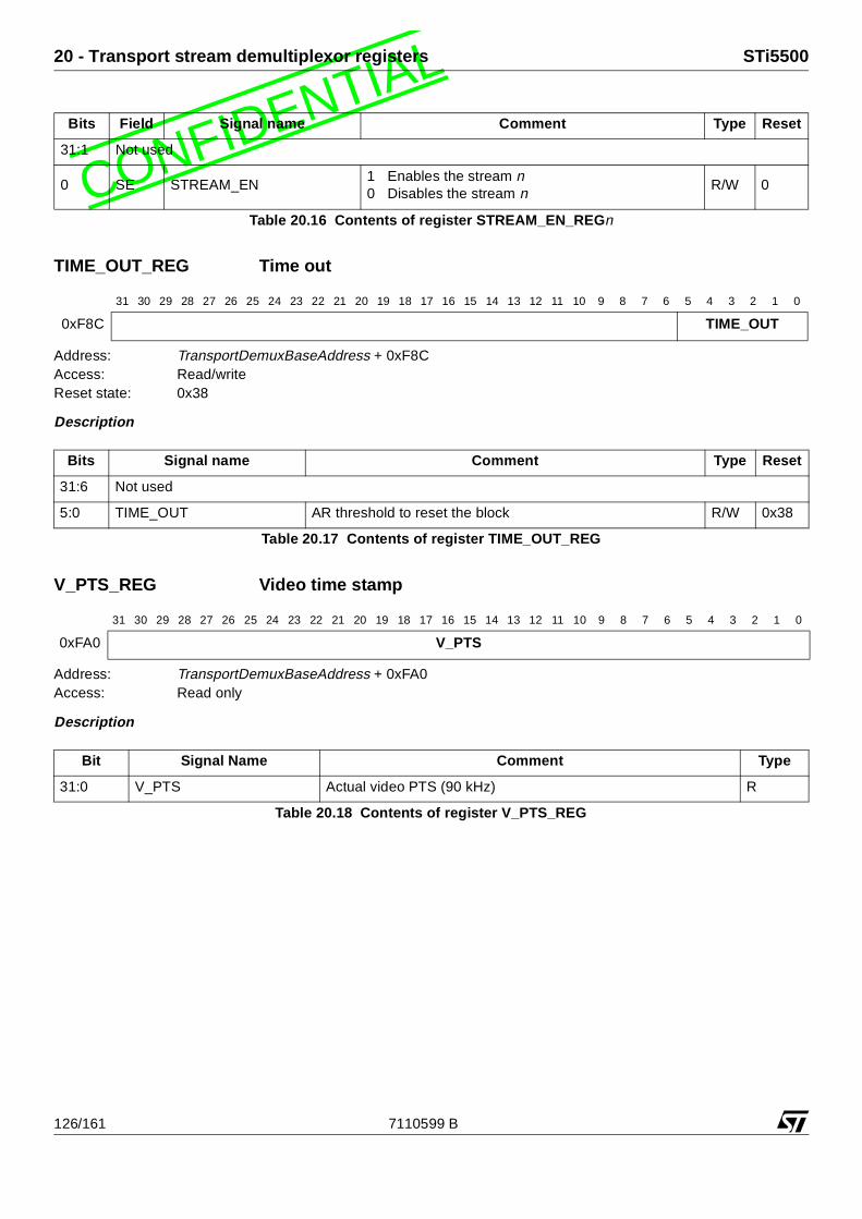
L20 - Transport stream demultiplexor registers STi5500
CONFIDENTIA
TIME_OUT_REG Time out
Address: TransportDemuxBaseAddress + 0xF8CAccess: Read/writeReset state: 0x38
Description
V_PTS_REG Video time stamp
Address: TransportDemuxBaseAddress + 0xFA0Access: Read only
Description
Bits Field Signal name Comment Type Reset
31:1 Not used
0 SE STREAM_EN1 Enables the stream n0 Disables the stream n
R/W 0
Table 20.16 Contents of register STREAM_EN_REGn
31 30 29 28 27 26 25 24 23 22 21 20 19 18 17 16 15 14 13 12 11 10 9 8 7 6 5 4 3 2 1 0
0xF8C TIME_OUT
Bits Signal name Comment Type Reset
31:6 Not used
5:0 TIME_OUT AR threshold to reset the block R/W 0x38
Table 20.17 Contents of register TIME_OUT_REG
31 30 29 28 27 26 25 24 23 22 21 20 19 18 17 16 15 14 13 12 11 10 9 8 7 6 5 4 3 2 1 0
0xFA0 V_PTS
Bit Signal Name Comment Type
31:0 V_PTS Actual video PTS (90 kHz) R
Table 20.18 Contents of register V_PTS_REG
126/161 7110599 B

LSTi5500 21 - Teletext interface (Ttxt) registers
CONFIDENTIA21 Teletext interface (Ttxt) registers
TtxtAbort Teletext AbortAddress: TtxtBaseAddress + 0x24Access: Write only
Description
The TtxtAbort register is write only. Any write to this address causes the teletext interface to abort the current opera-tion. The state of the teletext output operation is reset, and the teletext data transfer is interrupted. The DMA engine isreset only after the current word read or write is complete.
TtxtAckOddEven Teletext Acknowledge odd or evenAddress: TtxtBaseAddress + 0x20Access: Write only
Description
This register acknowledges the odd/even toggle interrupt. Any write to the TtxtAckOddEven register clears the Oddand Even bits of the TtxtIntStatus register.
TtxtDmaAddress Teletext DMA address
Address: TtxtBaseAddress + 0x00Access: Read/writeReset state: ?
DescriptionThe TtxtDmaAddress register is a 32-bit register, which specifies the base address in memory for the DMA transferfrom memory.
TtxtDmaCount Teletext DMA count
Address: TtxtBaseAddress + 0x04Access: Read/writeReset state: ?
Description
The TtxtDmaCount register specifies the number of bytes to be transferred from memory during the DMA operation. Awrite to this register also starts the teletext output operation. This value must be:
46 bytes x number_of_teletext_lines_to_send
31 30 29 28 28 26 25 24 23 22 21 20 19 18 17 16 15 14 13 12 11 10 9 8 7 6 5 4 3 2 1 0
0x00 DmaAddress
Bit Bit field Function
31:0 DmaAddress The base address for DMA transfer of data from memory.
31 30 29 28 28 26 25 24 23 22 21 20 19 18 17 16 15 14 13 12 11 10 9 8 7 6 5 4 3 2 1 0
0x04 DmaCount
7110599 B 127/161

L21 - Teletext interface (Ttxt) registers STi5500
CONFIDENTIA
TtxtIntEnable Teletext Interrupt enable
Address: TtxtBaseAddress + 0x1CAccess: Read/writeReset state: ?
DescriptionThe TtxtIntEnable register allows masking of the TtxtIntStatus register.
TtxtIntStatus Teletext Interrupt status
Address: TtxtBaseAddress + 0x18Access: Read onlyReset state: ?
Description
The TtxtIntStatus register gives the current state of the teletext operations. If the appropriate bits in the interruptenable register are set then interrupts can be driven by the state of this register.
TtxtMode Teletext Mode
Address: TtxtBaseAddress + 0x14Access: Read/writeReset state: ?
7 6 5 4 3 2 1 0
0x1C EvenEnable OddEnable OutCompleteEn
Bit Bit field Function
2 EvenEnable Enable even field interrupt.
1 OddEnable Enable odd field interrupt.
0 OutCompleteEn Enable teletext output operation completed interrupt.
31
30
29
28
28
26
25
24
23
22
21
20
19
18
17
16
15
14
13
12
1110
9 8 7 6 5 4 3 2 1 0
0x18 Even OddOut
Complete
Bit Bit field Function
2 Even Current (video encoder) field is EVEN.
1 Odd Current (video encoder) field is ODD.
0 OutComplete Teletext output operation completed.
31 30 29 28 28 26 25 24 23 22 21 20 19 18 17 16 15 14 13 12 11 10 9 8 7 6 5 4 3 2 1 0
0x14OddEven
128/161 7110599 B
LSTi5500 21 - Teletext interface (Ttxt) registers
CONFIDENTIADescriptionThe TtxtMode register sets the mode of the teletext interface. It specifies whether teletext data input memory is for oddor even fields.
TtxtOutDelay Teletext Output delay
Address: TtxtBaseAddress + 0x08Access: Read/writeReset state: ?
DescriptionThe TtxtOutDelay register is used to program the delay, in 27 MHz clock periods, from the rising edge of TtxtRequestto the first valid teletext data bit, i.e. TtxtData starting to transmit.
Bit Bit field Function
1 OddEvenSpecify odd or even fields of teletext data.
0 Teletext data to or from memory is for EVEN fields.1 Teletext data to or from memory is for ODD fields.
31 30 29 28 28 26 25 24 23 22 21 20 19 18 17 16 15 14 13 12 11 10 9 8 7 6 5 4 3 2 1 0
0x08 Delay
7110599 B 129/161
L22 - SDRAM block move (USD) registers STi5500
CONFIDENTIA22 SDRAM block move (USD) registers
USD_BMS Block Move Size
Address: VideoBaseAddress + 0x09Access: Serial read/writeReset state: 0
Description
This register holds the number of words to be moved in a block move operation.The second write to the register with USD_BMS non-zero enables (but does not launch) the block move mode. Thisregister must be written before the associated USD_BRP. The register is reset by a hardware reset.
USD_BRP Memory Read Pointer
Address: VideoBaseAddress + 0x0AAccess: Serial read/writeReset state: Undefined
DescriptionThis register holds the source address of the block to be moved. USD_BRP[18:0] is an offset from the base of SDRAMin units of 16-bit words. It points to the base of the block to be copied. The address must be 64-bit aligned, so the twoleast significant bits are always zeros. When USD_BMS is non-zero, the third write to USD_BRP launches the blockmove process, taking into account the values in USD_BMS and USD_BWP. The pointer is reset by a hardware reset.
USD_BWP Memory Write Pointer
Address: VideoBaseAddress + 0x0BAccess: Serial read/writeReset state: Undefined
DescriptionWhen a block move is to be executed (i.e. USD_BMS is non-zero), this register holds the destination address wherethe block is to be copied. USD_BWP[18:0] defines an offset from the base of SDRAM in units of 16-bit words. It pointsto the base of the area to be written. The address must be 64-bit aligned, so the two least significant bits are alwayszeros. The pointer is reset by a hardware reset.
7 0
1st cycle USD_BMS[15:8]
2nd cycle USD_BMS[7:0]
7 5 4 0
1st cycle USD_BRP[18:16]
2nd cycle USD_BRP[15:8]
3rd cycle USD_BRP[7:0]
7 5 4 0
1st cycle USD_BWP[20:16]
2nd cycle USD_BWP[15:8]
3rd cycle USD_BWP[7:0]
130/161 7110599 B

LSTi5500 23 - Video decoder (VID) registers
CONFIDENTIA23 Video decoder (VID) registers
VID_ABG Start of audio bit buffer
Address: VideoBaseAddress + 0x1C and 0x1DAccess: Read/writeReset state: 0
Description
The register holds the starting address of the audio bitstream buffer, defined in units of 2 Kbits. If the audio bit bufferstarts at address 0, then this register does not need to be set up, since its reset state is 0. A soft reset must be doneimmediately after the loading of this register in order for the value to be taken into account. In other words it mustonly be changed before the first compressed data of a new sequence is input, and never during the decoding of asequence.
VID_ABL Audio Bit Buffer Level
Address: VideoBaseAddress + 0x1E and 0x1FAccess: Read onlyReset state: 0
DescriptionThis register holds the current level of occupation of the audio bit buffer, defined in units of 2 Kbits. It can be read at anytime for the monitoring of the audio bit buffer level. When VID_ABL is greater than or equal to the value held in theVID_ABT register, the status bit VID_STA.ABF (audio bit buffer full) becomes set. When VID_ABL is zero, the statusbit VID_STA.ABE (audio bit buffer empty) becomes set.
VID_ABS Audio Bit Buffer Stop
Address: VideoBaseAddress + 0x20 and 0x21Access: Read/writeReset state: 0
Description
This register holds the address of the top of the audio bit buffer, defined in units of 2 Kbits. The space allocated to theaudio bit buffer starts at the address defined by the VID_ABG register, or, by default, 0. The end address of the audiobit buffer is:
(128 x ABS) + 127
7 0
0x1C ABG[13:8]
0x1D ABG[7:0]
7 0
0x1E ABL[13:8]
0x1F ABL[7:0]
7 0
0x20 ABS[13:8]
0x21 ABS[7:0]
7110599 B 131/161

L23 - Video decoder (VID) registers STi5500
CONFIDENTIAVID_ABS must only be changed before the first compressed data of a new sequence is input, and never during thedecoding of a sequence.
VID_ABT Audio Bit Buffer Threshold
Address: VideoBaseAddress + 0x22 and 0x23Access: Read/writeReset state: 0Synchronization: Edge Triggered
DescriptionThis register holds the level of occupancy of the audio bit buffer, in units of 2 Kbits, which when reached causes thestatus bit VID_STA.ABF to become set. If the bit CFG_CCF.PBO is set, then transfer of data to the audio bit buffer is prevented if the bit buffer level is at orabove the level defined in the VID_ABT register. If VID_ABT is set to a value equal to the top of the bit buffer, then thisautomatic mechanism will ensure that overflow never occurs.
VID_BFC Backward Chroma Pointer
Address: VideoBaseAddress + 0x5E and 0x5FAccess: Read/writeReset state: 0Synchronization: DSYNC
Description
This register holds the start address of the chrominance buffer of the backward prediction frame picture, defined inunits of 256 bytes.
VID_BFP Backward Frame Pointer
Address: VideoBaseAddress + 0x12 and 0x13Access: Read/writeReset state: 0Synchronization: DSYNC
DescriptionThis register holds the start address of the luminance buffer of the backward prediction frame picture, defined in unitsof 256 bytes.
7 0
0x22 ABT [13:8]
0x23 ABT [7:0]
7 0
0x5E BFC [13:8]
0x5F BFC [7:0]
7 0
0x12 BFP [13:8]
0x13 BFP [7:0]
132/161 7110599 B

LSTi5500 23 - Video decoder (VID) registers
CONFIDENTIAVID_CDcount Bit Buffer Input Counter
Address: VideoBaseAddress + 0x67Access: Serial read onlyReset state: 0
DescriptionThese three registers are accessed serially. They hold the number of bytes input to the bit buffer.The byte pointer is reset by a hardware reset, a global soft reset or a video soft reset.
VID_CSO SRC Chrominance Offset
Address: VideoBaseAddress + 0x6CAccess: Read/writeReset state: 0Synchronization: VSYNC
DescriptionThis register is set up with a value calculated from the fractional part of the pan vector. If no pan vector is defined, thisregister can be left in its reset (default) state. The method of calculation of the CSO value is given in the VID_PAN reg-ister description.
VID_CSR SRC Chrominance Resolution
Address: VideoBaseAddress + 0x6DAccess: Read/writeReset state: 0Synchronization: VSYNC
DescriptionThis register holds the upsampling factor of the luminance SRC (sample rate converter).The upsampling factor is equal to 256/CSR. Table 23.7 gives some examples of upsampling factors, where in eachcase the displayed picture has a nominal width of 720 pels. Also shown are the numbers of valid pels generated, “N”,calculated as shown in the STi5500 datasheet. Displayed picture widths other than 720 are supported.
7 0
1st cycle CDcount [23:16]
2nd cycle CDcount [15:8]
3rd cycle CDcount [7:0]
7 0
0x6C CSO[7:0]
7 0
0x6B LSR[7:0]
7110599 B 133/161

L23 - Video decoder (VID) registers STi5500
CONFIDENTIA
VID_CTL Decoding Control
Address: VideoBaseAddress + 0x02Access: Read/writeSynchronization: Edge triggered
Decoded Picture Width CSR N
640 228 715
640 227 718
544 193 717
544 192 721
480 170 717
480 169 722
352 125 713
352 124 719
704 250 717
704 249 720
Table 23.1 Example upsampling factors
7 6 5 4 3 2 1 0
0x02 ERU ERS PRS SRS EDC
134/161 7110599 B

LSTi5500 23 - Video decoder (VID) registers
CONFIDENTIADescription
VID_DCF Display Configuration
Address: VideoBaseAddress + 0x74 and 0x75Access: Read/writeReset state: 0Synchronization: VSYNC
Description
Field Bit Description
ERU 7Enable pipeline reset on picture decode error. When this bit is set, a pipeline reset is automat-ically generated in case of Picture Decode Error (less than DFS macroblocks decoded).
ERS 6Enable pipeline reset on severe error. When this bit is set, a pipeline reset is automatically generated in case of Severe Error (more than DFS macroblocks decoded).
5 Reserved. Write 0.
4:3 Reserved. Write 0.
PRS 2Pipeline reset. In order to generate a pipeline reset, this bit must be kept set for a duration of at least 4 SDRAM clock cycles (40 ns with a 100 MHz SDRAM clock).
SRS 1Soft reset. In order to generate a soft reset, this bit must be kept set for a duration of at least 54 SDRAM clock cycles (540 ns with a 100 MHz primary clock).
EDC 0 Enable decoding. This bit must be set to allow decoding.
Table 23.2 Bit fields in register VID_CTL
7 6 5 4 3 2 1 0
0x74 BLL BFL FNF FLY ORF
0x75 PXD EVD EOS DSR LFB CFB
Field Bit Description
BLL 13Blank Last Line. If this bit is set, the last active line of a picture is blanked. (Used in letter box format display).
BFL 12Blank First Line. If this bit is set the first active line of a picture is blanked. (Used in letter box format display).
FNF 11Frame not Field. This bit is only used during on-the-fly decoding. The bit must be set if a frame picture is going to be displayed, or reset if field picture are to be decoded on-the-fly. For classical decoding (field or frame) the bit is always 1.
FLY 10On The Fly. When this bit is set, the current picture is displayed directly from the pipeline. Otherwise, it is loaded from the external memory.
ORF 9
One Row per Frame. This bit is only active when bit VID_DCF.FNF is set. It defines the number of rows to be stored in the block to row RAM during a frame picture display. If it is set, one field macroblock line is stored (8 video lines). Otherwise, two field macroblock lines are stored (16 video lines). This bit is for test purposes. This bit must be reset for normal operation.
PXD 6 Set to ’1’.
Table 23.3 Fields of register VID_DCF
7110599 B 135/161

L23 - Video decoder (VID) registers STi5500
CONFIDENTIA
VID_DFC Displayed Chroma Frame Pointer
Address: VideoBaseAddress + 0x58 and 0x59Access: Read/writeReset state: 0Synchronization: VSYNC
Description
This register holds the start address, defined in units of 256 bytes, of the chroma frame which is currently being dis-played. When a new value is written this is used at the start of the next field. When VID_DFC is set to same value asVID_RFC (i.e. the decoder is writing the reconstructed picture into the buffer which is being displayed), bitVID_TIS.OVW must be set.
VID_DFP Displayed Luma Frame Pointer
Address: VideoBaseAddress + 0x0C and 0x0DAccess: Read/writeReset state: 0Synchronization: VSYNC
DescriptionThis register holds the start address, defined in units of 256 bytes, of the luma frame which is currently being dis-played. When a new value is written this is used at the start of the next field.When VID_DFP is set to the same value as VID_RFP (i.e. the decoder is writing the reconstructed picture into thebuffer which is being displayed), bit VID_TIS.OVW must be set.
EVD 5Enable video display. When this bit is reset, the video output has a constant value of Y=16, CB=CR=128. OSD is still displayed.
EOS 4Enable OSD. When this bit is set, the on-screen display (OSD) bitmap defined in the top and bottom field OSD buffers is displayed over the picture.
DSR 3Disable SRC. When this bit is set, both luminance and chrominance SRCs (sample rate converters) are disabled. In this case no horizontal filtering can occur, as would be required when the horizontal resolution of the decoded picture is equal to the horizontal resolution of the display.
LFB 10 AND bit ’CFB’ = ’0’: field based filtering mode1: frame based luma filtering modesee datasheet Chapter Display, section Block-to-row converter for detailed information.
CFB 00 AND bit ’LFB’ = ’0’: field based filtering mode1: frame based chroma filtering modesee datasheet Chapter Display, section Block-to-row converter for detailed information.
7 0
0x58 VID_DFC[13:8]
0x59 VID_DFC[7:0]
7 0
0x0C VID_DFP[13:8]
0x0D VID_DFP[7:0]
Field Bit Description
Table 23.3 Fields of register VID_DCF
136/161 7110599 B

LSTi5500 23 - Video decoder (VID) registers
CONFIDENTIAVID_DFS Decoded Frame Size
Address: VideoBaseAddress + 0x24Access: Serial read/writeReset state: 0Synchronization: DSYNC
Description
The circularity is reset by a software reset.
VID_DFW Decoded Frame Width
Address: VideoBaseAddress + 0x25Access: Read/writeReset state: 0Synchronization: DSYNC
Description
This register is set up with the width in macroblocks of the decoded picture. This is derived from the horizontal_sizevalue transmitted in the sequence header.
VID_END Little endian - big endian conversion
Address: VideoBaseAddress + 0x7CAccess: Read/writeReset state: 0Synchronization: None
DescriptionThis register contains only the bit ’END’, When set to ’1’, there is a hardware byte-swapping on the SMI which convertsdata from little endian to big endian formats (ST20 -> SDRAM) and vice versa (SDRAM -> ST20).This mode affects only the data which is written by the ST20 (little endian) into SDRAM memory and which are read bythe MPEG decoder (big endian). It is used for OSD transfer.
7 6 5 0
1st cycle DFS[13:8]
2nd cycle DFS[7:0]
Field Bits Description
DFS 13:0This register field is set up with a value equal to the number of macroblocks in the decoded picture. This is derived from the horizontal_size and vertical_size values transmitted in the sequence header.
Table 23.4 Bit fields in register VID_DFS
7 0
0x25 DFW[7:0]
7 6 5 4 3 2 1 0
0x7C reserved END
7110599 B 137/161

L23 - Video decoder (VID) registers STi5500
CONFIDENTIAVID_FFC Forward Chroma Frame Pointer
Address: VideoBaseAddress + 0x5C and 0x5DAccess: Read/writeReset state: 0Synchronization: DSYNC
DescriptionThis register holds the start address of the forward prediction chroma frame picture buffer, defined in units of 256bytes.
VID_FFP Forward Luma Frame Pointer
Address: VideoBaseAddress + 0x10 and 0x11Access: Read/writeReset state: 0Synchronization: DSYNC
Description
This register holds the start address of the forward prediction luma frame picture buffer, defined in units of 256 bytes.
VID_FRZ Freeze display
Address: VideoBaseAddress + 0x45Access: Read/writeReset state: 0Synchronization: None
DescriptionThis register is used to freeze the display. When bit 0 is set, the current decoded field is displayed continuously on bothfields until this bit is reset by the software. The effect of this bit is to freeze the current polarity of the internal B/notT sig-nal.This bit is also used to control three-to-two pull-down operation.
VID_HDF Header Data FIFO
Address: VideoBaseAddress + 0x66Access: Serial read only
7 0
0x5C FFC[13:8]
0x5D FFC[7:0]
7 0
0x10 FFP[13:8]
0x11 FFP[7:0]
7 0
0x45 FRZ
7 0
1st cycle HDF[15:8]
2nd cycle HDF[7:0]
138/161 7110599 B

LSTi5500 23 - Video decoder (VID) registers
CONFIDENTIAReset state: Undefined
DescriptionWhen the start code detector has found a start code, the header data FIFO must be read in order to identify the startcode and if required to obtain the header data. The start code identification procedure is described in the STi5500datasheet.Before reading the header FIFO, status bit VID_STA.HFE should be checked to ensure that it is not empty. If bitVID_STA.HFF is set then the header FIFO contains at least 66 bytes of data.As the start code detection is managed with 16-bit words, two successive reads are needed to access the whole 16-bitword; you must always perform an even number of reads before start code search restart (by software or with DSYNCsignal). The byte pointer is reset by a hardware reset, a global soft reset or a video reset.
VID_HDS Header Search
Address: VideoBaseAddress + 0x69Access: Read only bit SCM,
write only HDS, QMI and SOS.Reset state: 0Synchronization: None
DescriptionThis register controls the header search when it is written to, and returns the location of the start code when read.
7 3 2 1 0
Read cycle SCM
Write cycle SOS QMI HDS
Field Bit Description
SCM 3Start Code on MSB. This bit indicates in which byte the start code is located. If this bit is set then VID_HDF[15:8] contains the start code; otherwise VID_HDF[7:0] contains the start code.
Table 23.5 Fields of register VID_HDS when reading
Field Bit Description
SOS 2Stop on First Slice. This bit when set allows the start code detector to stop on the first slice start code of a picture (0x00000101). To allow mismatches, this bit must be used in conjunction with VID_HDS.SCM.
QMI 1
This bit is used to control access to the inverse quantize tables.
1 select the intra table0 select the non-intra table.
For example, to write a new intra table, write VID_HDS.QMI = 1 then write 64 weights to VID_QMW.
HDS 0Writing a 1 to this bit starts a header search. Completion of the header search is indicated by the setting of bit VID_STA.SCH.
Table 23.6 Fields of register VID_HDS when writing
7110599 B 139/161

L23 - Video decoder (VID) registers STi5500
CONFIDENTIAVID_ITM Interrupt Mask
Address: VideoBaseAddress + 0x3C, 0x60 and 0x61Access: Read/writeReset state: 0 (all interrupts disabled)Synchronization: None
DescriptionAny bit set in this register will enable the corresponding interrupt. An interrupt is generated whenever a bit in theVID_STA register changes from 0 to 1 and the corresponding mask bit is set.
VID_ITS Interrupt Status
Address: VideoBaseAddress + 0x3D, 0x62 and 0x63Access: Read onlyReset state: 0After the clocks have been enabled, the state changes to be the same as that of VID_STA.
Description
When a bit in the VID_STA register changes from 0 to 1, the corresponding bit in the VID_ITS register is set, irrespec-tive of the state of VID_ITM. If the corresponding bit of VID_ITM is set, the interrupt is asserted. Reading the most sig-nificant byte of VID_ITS clears it, leaving IRQ in its de-asserted (high) state.See the STi5500 datasheet for more information on interrupt handling.
VID_LDP Load Pointer
Address: VideoBaseAddress + 0x3FAccess: Read/writeReset state: 0Synchronization: None
Description
When this bit is set, the current start code detector pointer is stored in an internal register. When a PSC hit occurs, thecurrent start code detector pointer has to be stored for further use by the VLD (if a B frame is to be processed on thefly). This bit has to be set then reset before the PSD interrupt corresponding to the picture which has to be decodedon the fly (i.e. during the SCH interrupt).
7 6 5 4 3 2 1 0
0x3C NDP ERR ABF SFF AFF ABE
0x60 PDE SER BMI HFF PNC ERC PID RPID
0x61 PSD VST VSB BBE BBF HFE CFF SCH
7 6 5 4 3 2 1 0
0x3D NDP ERR ABF SFF AFF ABE
0x62 PDE SER BMI HFF PNC ERC PID RPID
0x63 PSD VST VSB BBE BBF HFE CFF SCH
7 0
0x3F LDP
140/161 7110599 B

LSTi5500 23 - Video decoder (VID) registers
CONFIDENTIAVID_LSO SRC Luminance Offset
Address: VideoBaseAddress + 0x6AAccess: Read/writeReset state: 0Synchronization: VSYNC
DescriptionThis register is set up with a value calculated from the fractional part of the pan vector. If no pan vector is defined, thisregister can be left in its reset (default) state.The method of calculation of the LSO value is given in the VID_PAN register description.
VID_LSR SRC Luma Resolution
Address: VideoBaseAddress + 0x6BAccess: Read/writeReset state: 0Synchronization: VSYNC
DescriptionThis register holds the upsampling factor of the luminance SRC (sample rate converter).The upsampling factor is equal to 256/LSR. Table 23.7 gives some examples of upsampling factors, where in eachcase the displayed picture has a nominal width of 720 pels. Also shown are the numbers of valid pels generated, “N”,calculated as shown in the STi5500 datasheet. Displayed picture widths other than 720 are supported.
7 0
0x6A LSO[7:0]
7 0
0x6B LSR[7:0]
Decoded Picture Width LSR N
640 228 715
640 227 718
544 193 717
544 192 721
480 170 717
480 169 722
352 125 713
352 124 719
704 250 717
704 249 720
Table 23.7 Example upsampling factors
7110599 B 141/161

L23 - Video decoder (VID) registers STi5500
CONFIDENTIAVID_NWM Not writable register mode
Address: VideoBaseAddress + 0x7BAccess: Read/writeReset state: 0Synchronization: None
DescriptionThis register contains only the bit ’NWM’, which, when set to ’1’, puts the registers ’CFG_MCF’, ’CFG_CCF’ and’CFG_DRC’ into a non-writable mode. The bit can be reset either by writing ’0’ or by a software reset.
VID_OBP OSD Bottom Field Pointer
Address: VideoBaseAddress + 0x2BAccess: Serial read/writeReset state: 0Synchronization: VSYNC bottom
DescriptionThis register is written or read in two cycles:
• first cycle: OBP[13:8]• second cycle: OBP[7:0]
The circularity is reset by a hardware reset or a bottom field VSYNC. The register holds the start address, in units of256 bytes of the current OSD specification buffer for the bottom field. This specification will be decoded during bottomfields when OSD is enabled.
VID_OSD On-screen Display Configuration
Address: VideoBaseAddress + 0x3EAccess: Read/writeReset state: 0
7 6 5 4 3 2 1 0
0x7B reserved NWM
7 5 0
1st cycle OBP[13:8]
2nd cycle OBP[7:0]
7 6 0
0x3E OAM OAD[5:0]
142/161 7110599 B

LSTi5500 23 - Video decoder (VID) registers
CONFIDENTIADescription.
VID_OTP OSD Top Field Pointer
Address: VideoBaseAddress + 0x2AAccess: Serial read/writeReset state: 0Synchronization: VSYNC top
Description
This register is written or read in two cycles:• first cycle: OTP[13:8]• second cycle: OTP[7:0]
The circularity is reset by a hardware reset or a top VSYNC. The register holds the start address, in units of 256 bytes,of the current OSD specification buffer for the top field. This specification will be decoded during top fields when OSDis enabled.
VID_PAN Pan/Scan Horizontal Vector Integer Part
Address: VideoBaseAddress + 0x2C and 0x2DAccess: Read/writeReset state: 0Synchronization: VSYNC
Description
This register is set up with the integer part of the horizontal pan/scan vector. The horizontal pan/scan vector defines, inthe decoded picture, the location of the first displayed luminance sample relative to the first luminance sample in theline.The VID_LSO and VID_CSO registers are set up with the fractional part of the horizontal pan/scan vector, as follows:
PSV = horizontal pan/scan vectorwhere x indicates the integer part of x.
Field Bits Description
OAM 6OSD active signal mode. When this bit is set, the OSD active signal is an input. When it is reset, the OSD active signal is an output. The OSD active signal must never be driven when VID_CTL.EVI=1 and VID_OSD.OAM=0.
OAD 5:0OSD active signal delay. These bits are used to define the delay of the OSD active signal corresponding to output OSD pixels.
Table 23.8 Bit fields of register VID_OSD
Comment: There is no such bit as VID_CTL.EVI.
7 5 0
1st cycle OTP[13:8]
2nd cycle OTP[7:0]
7 2 0
0x2C PAN[10:8]
0x2D PAN[7:0]
7110599 B 143/161

L23 - Video decoder (VID) registers STi5500
CONFIDENTIAVID_LSO = 256 x (horizontal pan/scan vector - PSV)
VID_CSO = VID_LSO / 2 (+ 1 if PSV is odd)
VID_PFH Picture F-parameters Horizontal
Address: VideoBaseAddress + 0x04Access: Read/writeReset state: 0Synchronization: DSYNC
Description
This register contains parameters of the picture to be decoded. These parameters are extracted from the bit stream.
VID_PFV Picture F-parameters Vertical
Address: VideoBaseAddress + 0x05Access: Read/writeReset state: 0Synchronization: DSYNC
Description
This register contains parameters of the picture to be decoded. These parameters are extracted from the bitstream.In MPEG-1 mode (i.e. when VID_PPR2.MP2 is reset), VID_PFV is not used.
VID_PPR1 Picture Parameters 1
Address: VideoBaseAddress + 0x06
7 4 3 0
0x04 BFH[3:0] FFH[3:0]
Field Bits MPEG-1 MPEG-2
BFH7
Set to full_pel_backward_vector of the picture head-er. Set to backward_horizontal_f_code of
the picture coding extension.6:4 Set to backward_f_code of the picture header.
FFH3 Set to full_pel_forward_vector of the picture header. Set to forward_horizontal_f_code of
the picture coding extension.2:0 Set to forward_f_code of the picture header.
Table 23.9 Bit fields of register VID_PFH
7 4 3 0
0x05 BFV[3:0] FFV[3:0]
Field Bits Description
BFV 7:4 The backward_vertical_f_code of the picture coding extension.
FFV 3:0 The forward_vertical_f_code of the picture coding extension.
Table 23.10 Bit fields of register VID_PFV
7 6 5 4 3 2 1 0
0x06 OTF PCT[1:0] DCP[1:0] PST[1:0]
144/161 7110599 B
LSTi5500 23 - Video decoder (VID) registers
CONFIDENTIAAccess: Read/writeReset state: 0Synchronization: DSYNC
Description
This register contains parameters of the picture to be decoded. These parameters are extracted from the bit stream.In MPEG-1 mode (i.e. when VID_PPR2.MP2 is reset), only PCT has to be set; the other bits must be reset.
VID_PPR2 Picture Parameters 2
Address: VideoBaseAddress + 0x07Access: Read/writeReset state: 0Synchronization: DSYNC
DescriptionThis register contains parameters of the picture to be decoded. These parameters are extracted from the bitstream.In MPEG-1 mode, all bits must be reset to 0.
Field Bits Description
OTF 6When set this bit directs the decoded data in the block-to-row memory to be displayed directly. The picture data is not reconstructed in memory.
PCT 5:4 Set to the two least significant bits of picture_coding_type in the picture header.
DCP 3:2Set equal to intra_dc_precision of the picture coding extension. The value “11”, defining a precision of 3 bits, is not allowed.
PST 1:0
Set to the picture_structure bits of the MPEG-2 picture coding extension.
00 Frame picture. This value is illegal in the MPEG-2 variable.01 Top field.10 Bottom field.11 Frame picture.
Table 23.11 Bit fields of register VID_PPR1
7 6 5 4 3 2 1 0
0x07 MP2 TFF FRM CMV QST IVF AZZ
Field Bits Description
MP2 6MPEG-2 mode. When this bit is set, the STi5500 expects an MPEG-2 video bitstream. If it is reset, then an MPEG-1 bitstream is expected.
TFF 5 This bit is set equal to the top_field_first bit of the MPEG-2 picture coding extension.
FRM 4 This bit is set equal to the frame_pred_frame_dct bit of the picture coding extension.
CMV 3This bit is set equal to the concealment_motion_vectors bit of the MPEG-2 picture coding extension. It indicates that motion vectors are coded for intra macroblocks.
QST 2 This bit is set equal to the q_scale_type bit of the picture coding extension.
IVF 1 This bit is set equal to the intra_vlc_format bit of the picture coding extension.
AZZ 0 This bit is set equal to the alternate_scan bit of the picture coding extension.
Table 23.12 Bit fields of register VID_PPR2
7110599 B 145/161
L23 - Video decoder (VID) registers STi5500
CONFIDENTIAVID_PTH Panic threshold
Address: VideoBaseAddress + 0x2E and 0x2FAccess: Read/writeReset state: 0Synchronization: VSYNC
Description
The panic threshold defines a block-to-row DRAM fullness level. In the block-to-row converter, there are two countersindicating the number of luma and chroma words stored. If the luma counter pointer is less than PTH or the chromacounter pointer is less than PTH divided by 2, a PANIC flag is set.The panic threshold is programmed in units of DRAM cells.
VID_QMW Quantization Matrix Data
Address: VideoBaseAddress + 0x76Access: Write onlyReset state: UndefinedSynchronization: None
DescriptionThis address is used to load the quantization coefficients in the order in which they appear in the bit stream, i.e. zig-zagorder. The bit VID_HDS.QMI defines which matrix (Intra or Inter) is written.For example, to write a new intra table, write VID_HDS.QMI = 1, and then write 64 weights to VID_QMW.
VID_REV STi5500 Revision
Address: VideoBaseAddress + 0x78Access: Read only
7 5 4 3 2 0
0x2E FPAN PEN NFW PTH[10:8]
0x2F PTH[7:0]
Field Bits Description
FPAN 13Force Panic Mode. This bit, when set, forces panic mode while decoding. For test purposes only.
PEN 12Panic mode enable. When set this bit allows the decoding to set the panic flag and enter the panic mode.
NFW 11Near Forward. This bit allows the user to select which prediction direction will be retained for bidirectional macroblocks in panic mode. Forward if set, backward otherwise.
PTH 10:0 Panic mode threshold.
Table 23.13 Bit fields of register VID_PTH
7 0
0x76 QMW[7:0]
7 0
0x78 REV[7:0]
146/161 7110599 B

LSTi5500 23 - Video decoder (VID) registers
CONFIDENTIADescriptionThis register holds the version number of the device. The contents of this register match the marking on the package.
VID_RFC Reconstructed Chroma Frame Pointer
Address: VideoBaseAddress + 0x5A and 0x5BAccess: Read/writeReset state: 0Synchronization: DSYNC
Description
This register holds the start address of the reconstructed (decoded) chroma frame picture buffer, defined in units of 256bytes.
VID_RFP Reconstructed Frame Pointer
Address: VideoBaseAddress + 0x0E and 0x0FAccess: Read/writeReset state: 0Synchronization: DSYNC
Description
This register holds the start address of the reconstructed (decoded) luma frame picture buffer, defined in units of 256bytes.
VID_RSTA Audio reset
Address: VideoBaseAddress + 0x7AAccess: Read/writeReset state: 0Synchronization: None
Description
This register contains only the bit ’RSTA’, which, when set to ’1’, flushes the audio bit buffer and software resets theaudio decoder (the video is not affected). In order to generate an audio software reset, this bit must be kept set for aduration of at least 54 SDRAM clock cycles.
7 5 0
0x5A RFC[13:8]
0x5B RFC[7:0]
7 5 0
0x0E RFP[13:8]
0x0F RFP[7:0]
7 6 5 4 3 2 1 0
0x7A reserved RSTA
7110599 B 147/161
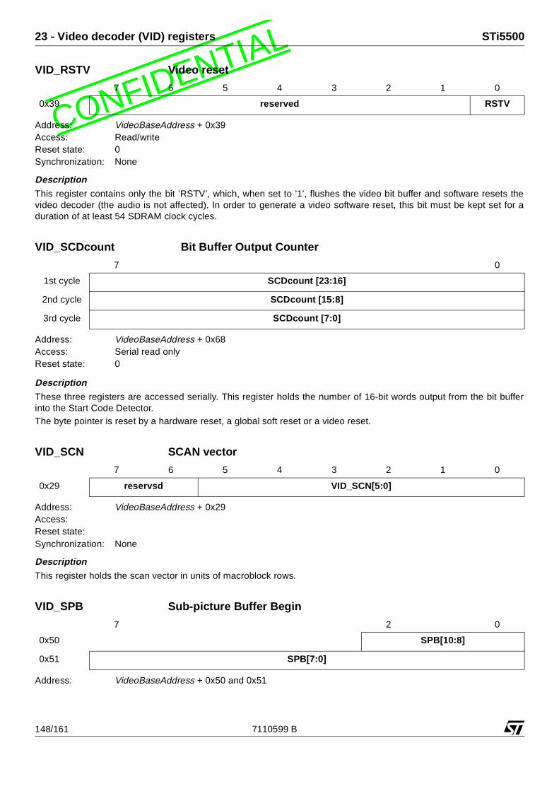
L23 - Video decoder (VID) registers STi5500
CONFIDENTIAVID_RSTV Video reset
Address: VideoBaseAddress + 0x39Access: Read/writeReset state: 0Synchronization: None
DescriptionThis register contains only the bit ’RSTV’, which, when set to ’1’, flushes the video bit buffer and software resets thevideo decoder (the audio is not affected). In order to generate a video software reset, this bit must be kept set for aduration of at least 54 SDRAM clock cycles.
VID_SCDcount Bit Buffer Output Counter
Address: VideoBaseAddress + 0x68Access: Serial read onlyReset state: 0
DescriptionThese three registers are accessed serially. This register holds the number of 16-bit words output from the bit bufferinto the Start Code Detector.The byte pointer is reset by a hardware reset, a global soft reset or a video reset.
VID_SCN SCAN vector
Address: VideoBaseAddress + 0x29Access:Reset state:Synchronization: None
DescriptionThis register holds the scan vector in units of macroblock rows.
VID_SPB Sub-picture Buffer Begin
Address: VideoBaseAddress + 0x50 and 0x51
7 6 5 4 3 2 1 0
0x39 reserved RSTV
7 0
1st cycle SCDcount [23:16]
2nd cycle SCDcount [15:8]
3rd cycle SCDcount [7:0]
7 6 5 4 3 2 1 0
0x29 reservsd VID_SCN[5:0]
7 2 0
0x50 SPB[10:8]
0x51 SPB[7:0]
148/161 7110599 B

LSTi5500 23 - Video decoder (VID) registers
CONFIDENTIAAccess: Read/writeReset state: 0Synchronization: none
Description
This register holds the start address of the sub-picture circular buffer and is programmed in units of 64 bytes. Thebuffer should be aligned on a 1 Kbyte boundary.
VID_SPE Sub-picture Buffer End
Address: VideoBaseAddress + 0x52 and 0x53Access: Read/writeReset state: 0Synchronization: none
DescriptionThis register holds the stop address of the sub-picture circular buffer and is programmed in units of 64 bytes. Thebuffer should be aligned on a 1 Kbyte boundary.
VID_SPRead SubPicture Read Pointer
Address: VideoBaseAddress + 0x4EAccess: Serial read/writeReset state: 0Synchronization: VSYNC
DescriptionThese three registers are accessed serially. The byte pointer is reset by a hardware reset. This is the absolute addressin the memory. This register is used when the software needs to set the read address of the sub-picture decoder and isprogrammed in units of 64-bit words. This value is taken into account after a VSYNC.
VID_SPWrite SubPicture Write Pointer
Address: VideoBaseAddress + 0x4FAccess: Serial read/writeReset state: 0
7 2 0
0x52 SPE[10:8]
0x53 SPE[7:0]
7 2 0
1st cycle SPR[18:16]
2nd cycle SPR[15:8]
3rd cycle SPR[7:0]
7 2 0
1st cycle SPW[18:16]
2nd cycle SPW[15:8]
3rd cycle SPW[7:0]
7110599 B 149/161
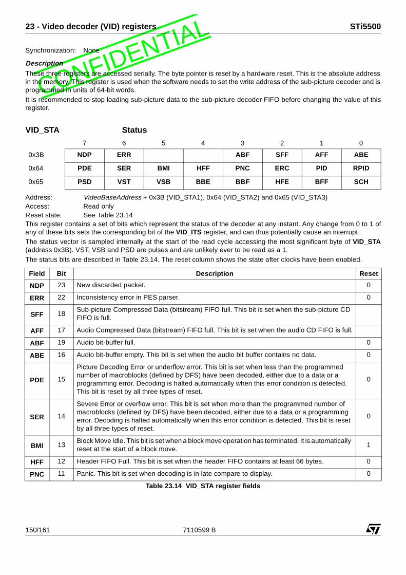
L23 - Video decoder (VID) registers STi5500
CONFIDENTIASynchronization: None
DescriptionThese three registers are accessed serially. The byte pointer is reset by a hardware reset. This is the absolute addressin the memory. This register is used when the software needs to set the write address of the sub-picture decoder and isprogrammed in units of 64-bit words.It is recommended to stop loading sub-picture data to the sub-picture decoder FIFO before changing the value of thisregister.
VID_STA Status
Address: VideoBaseAddress + 0x3B (VID_STA1), 0x64 (VID_STA2) and 0x65 (VID_STA3)Access: Read onlyReset state: See Table 23.14This register contains a set of bits which represent the status of the decoder at any instant. Any change from 0 to 1 ofany of these bits sets the corresponding bit of the VID_ITS register, and can thus potentially cause an interrupt.The status vector is sampled internally at the start of the read cycle accessing the most significant byte of VID_STA(address 0x3B). VST, VSB and PSD are pulses and are unlikely ever to be read as a 1. The status bits are described in Table 23.14. The reset column shows the state after clocks have been enabled.
7 6 5 4 3 2 1 0
0x3B NDP ERR ABF SFF AFF ABE
0x64 PDE SER BMI HFF PNC ERC PID RPID
0x65 PSD VST VSB BBE BBF HFE BFF SCH
Field Bit Description Reset
NDP 23 New discarded packet. 0
ERR 22 Inconsistency error in PES parser. 0
SFF 18Sub-picture Compressed Data (bitstream) FIFO full. This bit is set when the sub-picture CD FIFO is full.
AFF 17 Audio Compressed Data (bitstream) FIFO full. This bit is set when the audio CD FIFO is full.
ABF 19 Audio bit-buffer full. 0
ABE 16 Audio bit-buffer empty. This bit is set when the audio bit buffer contains no data. 0
PDE 15
Picture Decoding Error or underflow error. This bit is set when less than the programmed number of macroblocks (defined by DFS) have been decoded, either due to a data or a programming error. Decoding is halted automatically when this error condition is detected. This bit is reset by all three types of reset.
0
SER 14
Severe Error or overflow error. This bit is set when more than the programmed number of macroblocks (defined by DFS) have been decoded, either due to a data or a programming error. Decoding is halted automatically when this error condition is detected. This bit is reset by all three types of reset.
0
BMI 13Block Move Idle. This bit is set when a block move operation has terminated. It is automatically reset at the start of a block move.
1
HFF 12 Header FIFO Full. This bit is set when the header FIFO contains at least 66 bytes. 0
PNC 11 Panic. This bit is set when decoding is in late compare to display. 0
Table 23.14 VID_STA register fields
150/161 7110599 B

LSTi5500 23 - Video decoder (VID) registers
CONFIDENTIA
VID_TIS Task Instruction
Address: VideoBaseAddress + 0x03Access: Write onlyReset state: 0Synchronization: VSYNC
Description
This register contains 5 bitfields of the decoding task instruction.
ERC 10Error Concealment. This bit is set when an error is detected in the bit stream and the mech-anism of error concealment is active.
0
PID 9Pipeline Idle. This bit is set when the STi5500 is not in the course of decoding a picture, i.e. when the pipeline is inactive. It becomes low when the decoding of a picture starts and high when picture decoding is complete.
1
RPID 8Real Pipeline Idle. As bit ’PID’ above but without the condition "VLD found a new PSC". After clocks have been enabled, the state changes.
1
PSD 7Pipeline Starting to Decode. This bit is set for a short period at the instant the pipeline starts decoding a picture.
0
VST 6VSYNC Top. This bit is set for a short time at the beginning of the top field, corresponding to the falling edge of the B/T signal.
0
VSB 5VSYNC Bottom. This bit is set for a short time at the beginning of the bottom field, correspond-ing to the rising edge of the B/T signal.
0
BBE 4 Video bit buffer empty. This bit is set when the bit buffer contains no data. 1
BBF 3Video bit buffer full. This bit is set when the bit buffer level (= VID_VBL) is greater than or equal to the value loaded into the VID_VBT register.
1
HFE 2 Header FIFO Empty. This bit is set when the header FIFO is empty. 1
BFF 1Video Compressed Data (bit stream) FIFO Full. This bit is set when the video CD FIFO is full. This bit is equivalent to the signal CDREQ.
0
SCH 0
Start Code Hit. This bit is set whenever the first 16-bit word available in the header FIFO contains one of the start codes recognized (see the STi5500 datasheet). While data is being read from the header FIFO, this bit can be tested to determine whether the next word contains a start code.
0
7 6 5 4 3 2 1 0
0x03 SKP[1:0] OVW FIS RPT EXE
Field Bit Description Reset
Table 23.14 VID_STA register fields
7110599 B 151/161

L23 - Video decoder (VID) registers STi5500
CONFIDENTIA
VID_TRF Temporal Reference
Address: VideoBaseAddress + 0x56 and 0x57Access: Read/writeReset state: 0Synchronization: DSYNC
Field Bits Description
SKP 5:4
These bits are part of the instruction register, and are thus synchronized with VSYNC. They define the skipping of one or two pictures. If skipping is required, then these bits must be set up as part of the instruction for the picture which will be decoded immediately after the skipped pictures.
00 No skip (default)01 Skip one picture, decode next10 Skip two pictures, decode next11 Skip one picture then stop
OVW 3This bit must be set when the displayed picture and the reconstructed picture share the same buffer (i.e. VID_DFP = VID_RFP). It enables the overwrite mode which ensures that the recon-structed picture does not overwrite data which has not yet been displayed.
FIS 2Force instruction: if this bit is set, the task described by this register will be launch immediately. This bit is reset after its action. Its effect is the same as the effect of a VSYNC.
RPT 1When this bit is set, the task duration is two VSYNC periods. When the frame display rate is equal to the picture decoding rate, RPT will generally always be high. In case of a task launched by VID_TIS.FIS, RPT is not taken in account.
EXE 0
When this bit is not set, no decoding or skipping task is executed for one or two VSYNC periods, depending on the state of VID_TIS.RPT. If set, the next task (decoding or skipping) is executed. EXE is internally cleared when the task starts its execution, i.e. setting this bit activates only one execution.
Table 23.15 Fields of register VID_TIS
7 3 2 1 0
0x56 DC2 DTR TRF[9:8]
0x57 TRF[7:0]
152/161 7110599 B

LSTi5500 23 - Video decoder (VID) registers
CONFIDENTIADescriptionThis register contain extensions of the decoding task instruction. It is used only when decoding a B frame on the fly.
VID_VBG Start of Video Bit Buffer
Address: VideoBaseAddress + 0x14 and 0x15Access: Read/writeReset state: 0Synchronization: None
Description
The register holds the starting address of the video bit buffer, defined in units of 2 Kbits. If the video bit buffer starts ataddress 0, then this register does not need to be set up, since its reset state is 0. A soft reset must be done immedi-ately after the loading of this register in order for the value to be taken into account. In other words it must only bechanged before the first compressed data of a new sequence is input, and never during the decoding of a sequence.
VID_VBL Video Bit Buffer Level
Address: VideoBaseAddress + 0x16 and 0x17Access: Read onlyReset state: 0
DescriptionThis register holds the current level of occupation of the video bit buffer, defined in units of 2 Kbits. It can be read at anytime for the monitoring of the video bit buffer level. When VID_VBL is greater than or equal to the value held in theVID_VBT register, the status bit VID_STA.BBF (video bit buffer full) becomes set. When VID_VBL is zero, the statusbit VID_STA.BBE (video bit buffer empty) becomes set.
Field Bits Description
DC2 11
Redecode same B Frame twice. When this bit is set it signals the VLD that the next picture will have to be decoded twice. This bit is used when decoding a B Frame on the fly. It has to be set by the user before the first PSD interrupt corresponding to a B frame and reset on the according PSD interrupt.
DTR 10
Disable temporal reference comparision. This bit is used only when decoding a B frame on the fly. On every B frame redecode the VLD uses the temporal reference field VID_TRF.TRF[9:0] to resynchronize on the previously decoded picture. When this bit is set this comparision mechanism is disabled.
TRF 9:0Temporal reference. This field holds the temporal reference of the current decoded B frame. On every B frame redecode the VLD uses the temporal reference field TRF to resynchronize on the previously decoded picture. TRF is used only when bit DTR is reset.
Table 23.16 Fields of register VID_TRF
7 5 0
0x14 VBG[13:8]
0x15 VBG[7:0]
7 5 0
0x16 VBL[13:8]
0x17 VBL[7:0]
7110599 B 153/161
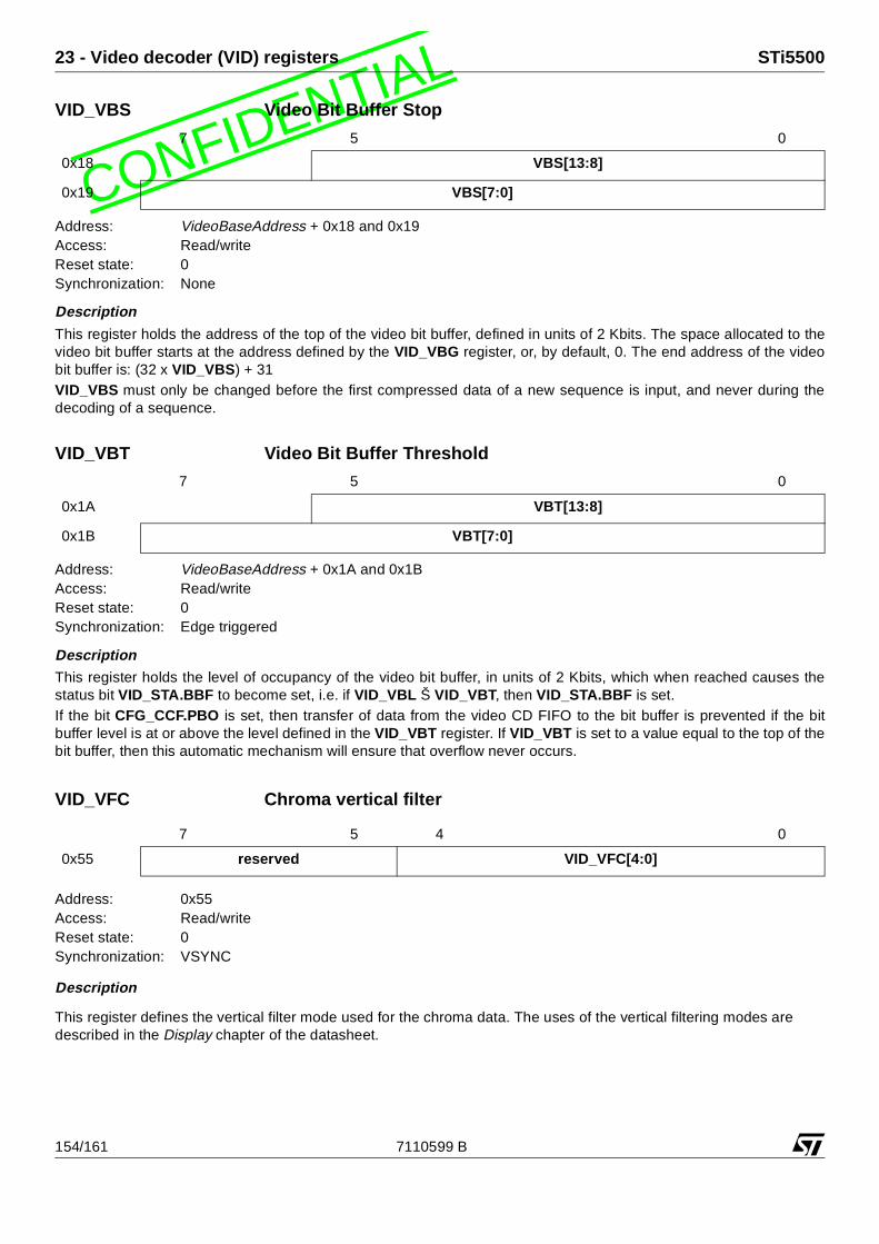
L23 - Video decoder (VID) registers STi5500
CONFIDENTIAVID_VBS Video Bit Buffer Stop
Address: VideoBaseAddress + 0x18 and 0x19Access: Read/writeReset state: 0Synchronization: None
Description
This register holds the address of the top of the video bit buffer, defined in units of 2 Kbits. The space allocated to thevideo bit buffer starts at the address defined by the VID_VBG register, or, by default, 0. The end address of the videobit buffer is: (32 x VID_VBS) + 31VID_VBS must only be changed before the first compressed data of a new sequence is input, and never during thedecoding of a sequence.
VID_VBT Video Bit Buffer Threshold
Address: VideoBaseAddress + 0x1A and 0x1BAccess: Read/writeReset state: 0Synchronization: Edge triggered
DescriptionThis register holds the level of occupancy of the video bit buffer, in units of 2 Kbits, which when reached causes thestatus bit VID_STA.BBF to become set, i.e. if VID_VBL Š VID_VBT, then VID_STA.BBF is set. If the bit CFG_CCF.PBO is set, then transfer of data from the video CD FIFO to the bit buffer is prevented if the bitbuffer level is at or above the level defined in the VID_VBT register. If VID_VBT is set to a value equal to the top of thebit buffer, then this automatic mechanism will ensure that overflow never occurs.
VID_VFC Chroma vertical filter
Address: 0x55Access: Read/writeReset state: 0Synchronization: VSYNC
Description
This register defines the vertical filter mode used for the chroma data. The uses of the vertical filtering modes are described in the Display chapter of the datasheet.
7 5 0
0x18 VBS[13:8]
0x19 VBS[7:0]
7 5 0
0x1A VBT[13:8]
0x1B VBT[7:0]
7 5 4 0
0x55 reserved VID_VFC[4:0]
154/161 7110599 B

LSTi5500 23 - Video decoder (VID) registers
CONFIDENTIAVID_VFL Luma vertical filter
Address: 0x54Access: Read/writeReset state: 0Synchronization: VSYNC
Description
This register defines the vertical filter mode used for the luma data. The uses of the vertical filtering modes are described in the Display chapter of the datasheet.
VID_XDO Display X Offset
Address: VideoBaseAddress + 0x70 to 0x71Access: Read/writeReset state: 0Synchronization: VSYNC
Description
VID_XDO is set up with a number defining the beginning of the left-hand border of the display. This offset is measuredfrom the active (first) edge of HSYNC and is specified in units of PIXCLK cycles. The horizontal offset, XDO’, is given by:
XDO’ = VID_XDO + 10
The offset, XDO’ cannot be less than 153 video decoder clock cycles.
VID_XDS Display X End
Address: VideoBaseAddress + 0x72 to 0x73Access: Read/writeReset state: 0Synchronization: VSYNC
Description
This register is set up with a number defining the right-hand boundary of the picture display window, expressed in unitsof PIXCLK cycles. The value of VID_XDS must be equal to VID_XDO plus the width of the display window. The actual offset, XDS', is given by:
XDS' = VID_XDS + 4
7 5 4 0
0x54 reserved VID_VFL[4:0]
7 1 0
0x70 XDO[9:8]
0x71 XDO[7:0]
7 1 0
0x72 XDS[9:8]
0x73 XDS[7:0]
7110599 B 155/161

L23 - Video decoder (VID) registers STi5500
CONFIDENTIAVID_XFW Displayed Frame Width
Address: VideoBaseAddress + 0x28Access: Read/writeReset state: 0Synchronization: VSYNC
DescriptionThis register is set up with a value equal to the width in macroblocks of the displayed picture. This is derived from thehorizontal_size value transmitted in the sequence header.
VID_YDO Display Y Offset
Address: VideoBaseAddress + 0x6EAccess: Read/writeReset state: 0Synchronization: VSYNC
Description
This register is set up with a number defining the first line of the picture display, i.e. the top edge of the display window.Lines are counted from the active (first) edge of VSYNC.In an interlaced display, the same value of VID_YDO would be used for both fields.
7 0
0x28 XFW[7:0]
7 0
0x6E YDO[7:0]
156/161 7110599 B
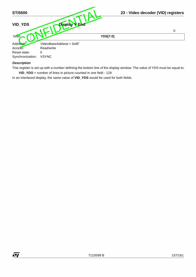
LSTi5500 23 - Video decoder (VID) registers
CONFIDENTIAVID_YDS Display Y End
Address: VideoBaseAddress + 0x6FAccess: Read/writeReset state: 0Synchronization: VSYNC
DescriptionThis register is set up with a number defining the bottom line of the display window. The value of YDS must be equal to:
VID_YDO + number of lines in picture counted in one field - 129
In an interlaced display, the same value of VID_YDS would be used for both fields.
7 0
0x6F YDS[7:0]
7110599 B 157/161
L24 - Index of Registers STi5500
CONFIDENTIA24 Index of RegistersA_PTS_REG 117AF_REG1-0 117AR_SIZE_REG 118ASCnBaudRate 23ASCnControl 24ASCnIntEnable 26ASCnRxBuffer 27ASCnStatus 28ASCnTimeout 29ASCnTxBuffer 30AUD_ADA 31AUD_ANC 31AUD_BBE 31AUD_CDI 32AUD_CRC 32AUD_DEM 32AUD_DIF 33AUD_DIV 33AUD_ESC 34AUD_EXT 34AUD_FFL 34AUD_FOR 35AUD_HDR 35AUD_IDE 35AUD_IFT 36AUD_IMS 36AUD_ISS 36AUD_ITM 37AUD_ITR 37AUD_ITS 38AUD_LCA 38AUD_LCK 38AUD_LRP 39AUD_MUT 39AUD_ORD 39AUD_P18 40AUD_PLY 40AUD_PTS 40AUD_RCA 41AUD_RES 41AUD_RST 41AUD_SCM 41AUD_SCP 42AUD_SEM 42AUD_SFR 42AUD_SID 43AUD_SKP 43AUD_SYE 43AUD_SYN 44AUD_SYS 45
AUD_VER 45BMDMADestAddress 46CacheControl 47CacheControlLock 47CCCF1 58CCCF2 58CCLIF1 58CCLIF2 59CFG_CCF 50CFG_CDR 50CFG_DRC 51CFG_GCF 51CFG_MCF 52CGMS_BIT 60CHIPID 60CKG_AUX 53CKG_CFG 53CKG_LNK 54CKG_MCK 55CKG_PCM 55CKG_PLL 56CKG_PXC 57Clear_Exec 81Clear_Mask 81Clear_Pending 81Clear_PnC2:0 92Clear_PnComp 92Clear_PnMask 92Clear_PnOut 93CONFIGURATION0 60CONFIGURATION1 62CONFIGURATION2 63CONFIGURATION3 64CONFIGURATION4 66CONFIGURATION5 67CONFIGURATION6 68EMIConfigData0 74EMIConfigData1 76EMIConfigData2 77EMIConfigData3 78EMIConfigLockBank3-0 79EMIConfigStatus 80EMIDRAMInitialize 80EN_LINK_REG 118Exec 81EXTRA_BITS_REG 119FlushDCache 48HandlerWptrn 82INCREMENT_DFS 69InputInterrupts 86
IntnPriority 86InvalidateDCache 48InvalidateICache 48LINE_REG 70LINK_STAT_FIFO 119LINK_STAT_REG 121Mask 82MODE_REG 121MPEGnBurstSize 87MPEGnDecoderSelect 87MPEGnHoldoff 87MPEGnSuspend 88PACKET_LENGTH 122PCR_EXT_REG 122PCR_REG 123PCR_STREAM_REG 123Pending 83PES_CF1 89PES_CF2 89PES_TM1 90PES_TM2 90PES_TS 91PHASE_DFS 70PnC2:0 93PnComp 94PnIn 94PnMask 94PnOut 95PWMCaptureCount 99PWMControl 99PWMCount 100PWMIntAck 100PWMIntEnable 101PWMIntStatus 101PWMnCaptureEdge 97PWMnCaptureVal 97PWMnCompareOutVal 98PWMnCompareVal 98PWMnVal 99revid 71ScnClkCon 103ScnClkVal 103SDAV_CONF_REG 123SDAV_DATA_REG 124SDAV_DMA_EN_REG 125SelectCache 49Set_Exec 84Set_Mask 84Set_Pending 84Set_PnC2:0 95
158/161 7110599 B

LSTi5500 24 - Index of Registers
CONFIDENTIASet_PnComp 95Set_PnMask 95Set_PnOut 96SPD_CTL1 104SPD_CTL2 104SPD_HLEX 105SPD_HLEY 105SPD_HLRC 105SPD_HLRCO 105SPD_HLSX 106SPD_HLSY 106SPD_LUT 106SPD_RST 107SPD_SPB 107SPD_SPE 107SPD_SPRead 108SPD_SPWrite 108SPD_SXD0 108SPD_SXD1 109SPD_SYD0 109SPD_SYD1 109SPD_XD0 110SPD_XD1 110SPD_YD0 110SPD_YD1 111SSC0BRG 112SSC0Con 112SSC0IEn 113SSC0RBuf 114SSC0SlAd 114SSC0Stat 115SSC0TBuf 115STATUS 71STREAM n configuration1 117STREAM n configuration2 117STREAM n configuration3 117STREAM_EN_REGn 125TIME_OUT_REG 126TriggerMode 85
ttx_block_map 72ttx_block1-4 72TtxtAbort 127TtxtAckOddEven 127TtxtDmaAddress 127TtxtDmaCount 127TtxtIntEnable 128TtxtIntStatus 128TtxtMode 128TtxtOutDelay 129USD_BMS 130USD_BRP 130USD_BWP 130V_PTS_REG 126VID_ABG 131VID_ABL 131VID_ABS 131VID_ABT 132VID_BFC 132VID_BFP 132VID_CDcount 133VID_CSO 133VID_CSR 133VID_CTL 134VID_DCF 135VID_DFC 136VID_DFP 136VID_DFS 137VID_DFW 137VID_END 137VID_FFC 138VID_FFP 138VID_FRZ 138VID_HDF 138VID_HDS 139VID_ITM 140VID_ITS 140VID_LDP 140VID_LSO 141
VID_LSR 141VID_NWM 142VID_OBP 142VID_OSD 142VID_OTP 143VID_PAN 143VID_PFH 144VID_PFV 144VID_PPR1 144VID_PPR2 145VID_PTH 146VID_QMW 146VID_REV 146VID_RFC 147VID_RFP 147VID_RSTA 147VID_RSTV 148VID_SCDcount 148VID_SCN 148VID_SPB 148VID_SPE 149VID_SPRead 149VID_SPWrite 149VID_STA 150VID_TIS 151VID_TRF 152VID_VBG 153VID_VBL 153VID_VBS 154VID_VBT 154VID_VFC 154VID_VFL 155VID_XDO 155VID_XDS 155VID_XFW 156VID_YDO 156VID_YDS 157
7110599 B 159/161

CONFIDENTIAL25 - Revision history STi5500
160/161 7110599 B
25 Revision historyThe corrections made to register manual revA in order to create this STi5500 register manual revB are given in the table below.
Modifications relating to circuit improvements are included in this document, and given in the table below.
Correction Description
Table 1.2 Wait state encoding deleted all references to "2 wait states"
Register ’AUD_SFR’ on page 42 reset state now defined ’00’
Register ’CONFIGURATION5’ on page 67 redefined bits ’bkr’ & ’bkg’
Register ’ttx_block1-4’ on page 72 redefined ’txbs’ & ’txbe’
Table 25.1 RevA to revB corrections
Modification Description
Register ’PES_CF1’ on page 89 Added bit ’FAD’ (bit6)
Register ’SPD_CTL1’ on page 104 Bit SPP, ’VID_DCF’ on page 135 moved to ’SPD_CTL1’
New register ’SPD_RST’ on page 107 Bit SPR, ’VID_CTL’ on page 134 moved to ’SPD_RST’
Register ’VID_DCF’ on page 135 Redefined bits2-0
Register ’VID_DCF’ on page 135 Bit ’PXD’ re-defined
New register ’VID_END’ on page 137 Little endian - big endian conversion
Registers ’VID_STA’ on page 150, ’VID_ITM’ on page140 & ’VID_ITS’ on page 140
Added bit ’RPID’ (bit8) to each register
New register ’VID_NWM’ on page 142 Not writable register mode
Removed ’VID_DC2’
Register ’VID_PPR2’ on page 145 Bit MP2, ’VID_TIS’ on page 151 moved to ’VID_PPR2’
New register ’VID_RSTA’ on page 147 Audio reset
Added register ’VID_RSTV’ on page 148 Video reset
Added register ’VID_SCN’ on page 148 Scan vector
Removed registers ’VID_MLU’ & ’VID_MCH’,Added registers ’VID_VFC’ on page 154 & ’VID_VFL’ onpage 155
New chroma/luma vertical filter registers
Table 25.2 Modifications

CONFIDENTIALSTi5500 -
7110599 B 161/161
Information furnished is believed to be accurate and reliable. However, STMicroelectronics assumes no responsibility for the consequences of use of such information nor for any infringement of patents or other rights of third parties which may result from its
use. No license is granted by implication or otherwise under any patent or patent rights of STMicroelectronics. Specifications mentioned in this publication are subject to change without notice. This publication supersedes and replaces all information
previously supplied. STMicroelectronics products are not authorized for use as critical components in life support devices or systems without express written approval of STMicroelectronics.
The ST logo is a registered trademark of STMicroelectronics
© 2000 STMicroelectronics - All Rights Reserved
STMicroelectronics GROUP OF COMPANIESAustralia - Brazil - Canada - China - France - Germany - Italy - Japan - Korea - Malaysia - Malta - Mexico - Morocco
The Netherlands - Singapore - Spain - Sweden - Switzerland - Taiwan - Thailand - United Kingdom - U.S.A.
http://www.st.com
Related Documents


