Status of test beam data analysis … with emphasis on resistive coating studies Progress and questions 1 Meeting at CEA Saclay, 25 Jan 2010 Jörg Wotschack, CERN

Status of test beam data analysis … with emphasis on resistive coating studies Progress and questions 1Meeting at CEA Saclay, 25 Jan 2010Jörg Wotschack,
Dec 14, 2015
Welcome message from author
This document is posted to help you gain knowledge. Please leave a comment to let me know what you think about it! Share it to your friends and learn new things together.
Transcript

Status of test beam data analysis
… with emphasis on resistive coating studies
Progress and questions
1Meeting at CEA Saclay, 25 Jan 2010 Jörg Wotschack, CERN

Chambers tested P1: 350 x 450 mm2 standard, various strip pitches (reference
chamber) – OK P4: 400 x 1400 mm2 standard, 250 and 500 µm strip pitches,
strips 400 and 1000 mm long (looks OK, data not yet analyzed) S3: Standard 100 x 100 mm2; 250 µm strip pitch R3: as S3 + resistive paste on strips (150-200 µm, 10 MΩ),
covered with metallic pads (1 x 0.15 mm2) R4: as S3 + Kapton layer with strips on both sides – failed R5: as S3 + resistive paste (1 mm, 5 kΩ) and metallic pads
above strips MM (S1) + GEM/MM as double-stage amplification (talk by VP)
2Meeting at CEA Saclay, 25 Jan 2010 Jörg Wotschack, CERN

Test beam November 2009
P1 & R3 discharge studiesHV and currents vs particle rates
Chambers connected to ALTRO readoutCPA = 100 pF/strip
3

HV/Current of P1 – 19 Nov
4
≈ 3 hours
HV
me
sh (
V)
Cur
rent
me
sh (
µA
)

HV/Current of P1 and R3
5
Cur
rent
me
sh (
µA
)
HV
me
sh (
V)
Rate: 5–10 kHz/cm2
P1 R3
≈ 2.5 hours

HV/Current R3 – 20 Nov
6
HV
me
sh (
V)
Cur
rent
me
sh (
µA
)
Rate: ≈ 10 kHz/cm2 ≈20 kHz/cm2 Rate: ≈ 25 kHz/cm2
???
≈ 2 hours

R3 ‘short’
7

Local damage of resistive layer Resistive layer is locally damaged, induced by some large charge
(Resistive paste not very homogeneous, manually applied) Regions with lower resistance (or some defects) are affected first. Once the resistive layer is locally damaged, sparks with higher currents
develop at the affected pad➪ 1st lesson: Resistive layer must be made more reliable
8
1mm
x 0
.15
mm
pad
Strip
Muon Week, 11 Dec 2009 Joerg Wotschack (CERN)
PCB
MeshinsulatorResistive paste
200 µm
128 µm

R3 performance
9
We observe Nice signals Noise is OK, not
much different from std MM
But Many events
with no or very small signals
Low efficiency ???

Test of R3 in lab with 55Fe source
Same gas mixture (Ar:CO2, 85:15) as in H6 Try to understand the behaviour of R3 Measured pulse spectra 72 strips connected together -> single
preamplifier + Ortec amplifier Coupling capacitor: CPA = 1.8 pF (!?) …..
some surprises Started with S3 (no resistive coating)Muon Week, 11 Dec 2009 Joerg Wotschack (CERN) 10

S3 (standard MM w/o resistive layer)
Muon Week, 11 Dec 2009 Joerg Wotschack (CERN) 11
S3
Gain = 103 Gain = 104
σ =20% FWHM
55Fe spectrum
HVmesh = 535 VAr:CO2 85:15

S3 + R3 (55Fe source data)
Muon Week, 11 Dec 2009 Joerg Wotschack (CERN) 12
S3
R3

Rate effect and local variations
13Muon Week, 11 Dec 2009 Joerg Wotschack (CERN)
R3 (h5)
1
2
3
54

Likely explanation Bad contact b/w small pads and resistive paste => large resistance Charge build-up on pad Reduced potential b/w mesh and pad => Smaller amplification➪ 2nd lesson: pads must have a reliable contact with resistive layer
14
Mesh
insulator
1mm
x 0
.15
mm
pad
Strip
PCB
Resistive paste
Muon Week, 11 Dec 2009 Joerg Wotschack (CERN)

S3 local response variations
15
1
2
3
54
Muon Week, 11 Dec 2009 Joerg Wotschack (CERN)

The response of R3 vs S3
16
Gain = 104Gain = 103
Muon Week, 11 Dec 2009 Joerg Wotschack (CERN)
Q(R3) ≈ 0.8 x Q(S3) S3
R3 (h5)
R3 (h3)
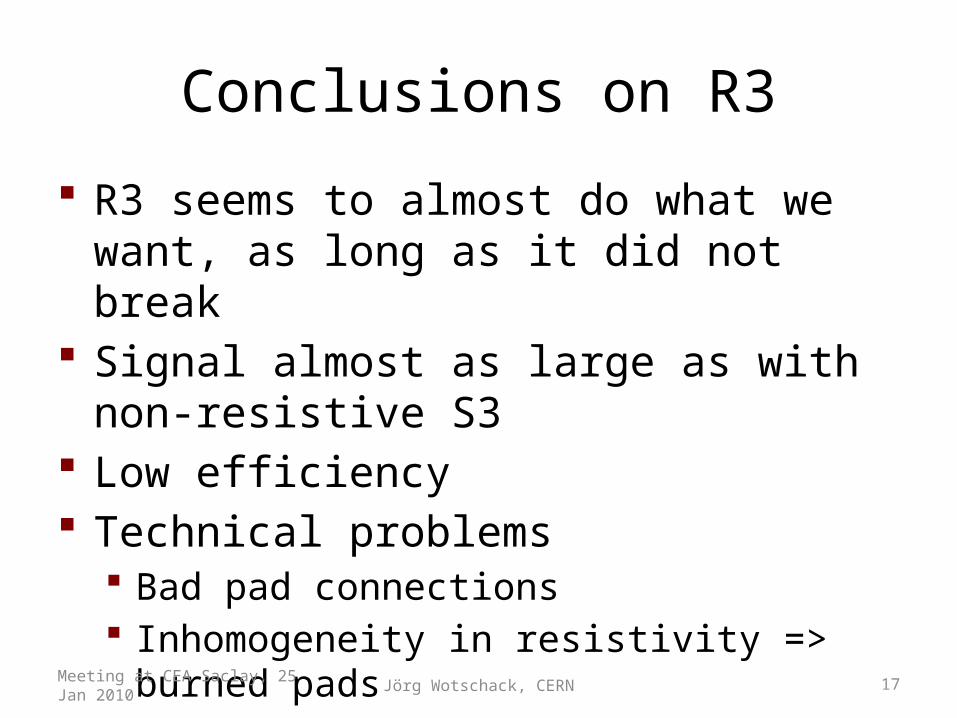
Conclusions on R3
R3 seems to almost do what we want, as long as it did not break
Signal almost as large as with non-resistive S3 Low efficiency Technical problems
Bad pad connections Inhomogeneity in resistivity => burned pads
Meeting at CEA Saclay, 25 Jan 2010 Jörg Wotschack, CERN 17

R5 Similar to R3 but with more robust resistive
layer and different technique (Rui’s talk) R ≈ 5 kΩ
Meeting at CEA Saclay, 25 Jan 2010 Jörg Wotschack, CERN 18
PCB
Resistive pasteInsulator
≈ 50 µm
1mm
x 0
.15
mm
pad
Mesh

R5 spectra
Meeting at CEA Saclay, 25 Jan 2010 Jörg Wotschack, CERN 19
Gain = 5000 10000
S3 (570 V)

R5: first observations
First measurements of R5 (55Fe source) Sparking starts at HVmesh ≈ 560 V
Large currents (several µA) Large HV drop (100–200 V)
R5 signal ≈2 x S3 signal For comparison: R3 signal ≈ 0.8 x S3 signal Charge resolution much worse than for S3
(and R3); escape peak not well separated
Meeting at CEA Saclay, 25 Jan 2010 Jörg Wotschack, CERN 20

Conclusions & plans
Main problem is the spark problem Quite a bit of progress … but R5 is not yet the final solution (more in Rui’s talk) Need more and more systematic studies of different
chambers Measure capacitances Use well defined readout electronics
Spice simulation of different schemes would help Looking forward to R6
Meeting at CEA Saclay, 25 Jan 2010 Jörg Wotschack, CERN 21
Related Documents