154 IEEE JOURNAL OF SOLID-STATE CIRCUITS, VOL. 21, NO. 2. FEBRUARY 1992 Statistical Modeling of Device Mismatch MOS Integrated Circuits for Analog Christopher Michael and Mohammed Ismail, Senior Member, ZEEE Abstract-A generalized parameter-level statistical MOS model, called SMOS, capable of generating statistically signif- icant model decks from intra- and inter-die parameters statis- tics is described. Calculated model decks preserve the inherent correlations between model parameters while accounting for the dependence of parameter variance on device separation dis- tance and device area. Using a Monte Carlo approach to pa- rameter sampling, circuit output means and standard devia- tions can be simulated. Incorporated in a CAD environment, these modeling algorithms will provide the analog circuit de- signer with a method to determine the effect of both circuit lay- out and device sizing on circuit output variance. This will ul- timately lead to computer-aidedoptimizationof both circuit and layout design of analog integrated circuits. Test chips have been fabricated from two different fabrication processes to extract statistical information required by the model. Experimental and simulation results for two analog subcircuits are compared to verify the statistical modeling algorithms. I. INTRODUCTION DVANCES in microelectronics fabrication coupled A with the desire to create faster, more complex analog CMOS circuits have pushed the feature size of many an- alog processes to the 1-2-pm range. Because variances in parameters such as channel length, channel width, thresh- old voltage, and substrate doping do not scale with di- mension, device mismatch increases as device feature size is reduced. It is expected that the performance variations caused by this mismatch in short-channel CMOS circuits will be crucial and may, ultimately, introduce a limitation for device scaling in analog circuits. In order to simulate short-channel analog CMOS cir- cuits with a high degree of reliability, a parameter-level statistical model which accounts for intra-die variances and correlations in model parameters is needed. Second moment simulation based on a model of this type will be useful in determining the sensitivity to scaling of existing circuits as well as predicting performance variations in new designs. Likewise, fabrication processes can be com- pared according to performance and reliability by simu- Manuscript received February 5, 1991; revised July 22, 1991. This work was supported in part by the Semiconductor Research Corporation under Contract 90-DJ-066 and by the National Science Foundation under Grant C. Michael was with the Department of Electrical Engineering, Ohio State University, Columbus, OH 43210. He is now with National Semi- conductor Corporation, Santa Clara, CA 95052. M. Ismail is with the Solid-state Microelectronics Laboratory, Depart- ment of Electrical Engineering, Ohio State University, Columbus, OH 43210. I MIP-8896244. IEEE Log Number 9 104347. lating the same circuit using statistical data from different processes. With this tool, an analog circuit designer can estimate the yield of a circuit based on a performance specification without fabrication of the device. Despite its importance to circuit operation, relatively few papers have been presented on the subject of MOS transistor mismatch. Shyu et al. [l] examined the de- pendence of the standard deviation of current sources on device size. Lakshmikumar et al. [2] advanced this work by separating the area dependence of transistor mismatch into two separate components: the standard deviations of the current factor and the threshold voltage. Pelgrom et al. [3] further parameterized mismatch by including a term for the standard deviation of the substrate factor. Addi- tionally, the effect of device spacing on transistor match- ing was investigated. While these studies successfully de- termined the primary causes of device mismatch, the resultant equations for drain current mismatch are not compatible with present circuit simulators. Previous publications in the area of statistical modeling and simulation [4]-[lo] have focused on methods to solve the problem of correlated parameters. Some investiga- tions [4]-[6] attempted to describe the total device vari- ance in terms of a few independent physically meaningful parameters. While this approach is sufficient for large-ge- ometry devices, the inclusion of second-order effects is necessary in the statistical modeling of short-channel de- vices, especially in analog circuits where model accuracy is crucial. Other investigations [SI-[ 101 have used prin- cipal component analysis; a more standardized statistical technique to account for parameter correlation. Using this technique, these studies have accomplished the goal of producing a CAD-compatible algorithm to calculate cor- related model parameters, including second-order effects. However, these studies depend on either die-level statis- tics or a combination of die-level and matched statistics [SI, [ l l ] to calculate model decks. In either case, the de- pendence of parameter standard deviations on device area and circuit layout is not included in the parameter calcu- lations. The resultant simulations are generally overly pessimistic, with no information concerning the effect of device area and spacing on the circuit output variances. This paper will present a unified method to accurately calculate statistically relevant device model decks. Sec- tion I1 presents both the statistical model and the algo- rithms used to calculate model decks. A comparison of experimental data to simulations performed using the new 0018-9200/92$03.00 0 1992 lEEE

Welcome message from author
This document is posted to help you gain knowledge. Please leave a comment to let me know what you think about it! Share it to your friends and learn new things together.
Transcript

154 IEEE JOURNAL OF SOLID-STATE CIRCUITS, VOL. 2 1 , NO. 2 . FEBRUARY 1992
Statistical Modeling of Device Mismatch MOS Integrated Circuits
for Analog
Christopher Michael and Mohammed Ismail, Senior Member, ZEEE
Abstract-A generalized parameter-level statistical MOS model, called SMOS, capable of generating statistically signif- icant model decks from intra- and inter-die parameters statis- tics is described. Calculated model decks preserve the inherent correlations between model parameters while accounting for the dependence of parameter variance on device separation dis- tance and device area. Using a Monte Carlo approach to pa- rameter sampling, circuit output means and standard devia- tions can be simulated. Incorporated in a CAD environment, these modeling algorithms will provide the analog circuit de- signer with a method to determine the effect of both circuit lay- out and device sizing on circuit output variance. This will ul- timately lead to computer-aided optimization of both circuit and layout design of analog integrated circuits. Test chips have been fabricated from two different fabrication processes to extract statistical information required by the model. Experimental and simulation results for two analog subcircuits are compared to verify the statistical modeling algorithms.
I. INTRODUCTION DVANCES in microelectronics fabrication coupled A with the desire to create faster, more complex analog
CMOS circuits have pushed the feature size of many an- alog processes to the 1-2-pm range. Because variances in parameters such as channel length, channel width, thresh- old voltage, and substrate doping do not scale with di- mension, device mismatch increases as device feature size is reduced. It is expected that the performance variations caused by this mismatch in short-channel CMOS circuits will be crucial and may, ultimately, introduce a limitation for device scaling in analog circuits.
In order to simulate short-channel analog CMOS cir- cuits with a high degree of reliability, a parameter-level statistical model which accounts for intra-die variances and correlations in model parameters is needed. Second moment simulation based on a model of this type will be useful in determining the sensitivity to scaling of existing circuits as well as predicting performance variations in new designs. Likewise, fabrication processes can be com- pared according to performance and reliability by simu-
Manuscript received February 5 , 1991; revised July 22, 1991. This work was supported in part by the Semiconductor Research Corporation under Contract 90-DJ-066 and by the National Science Foundation under Grant
C. Michael was with the Department of Electrical Engineering, Ohio State University, Columbus, OH 43210. He is now with National Semi- conductor Corporation, Santa Clara, CA 95052.
M. Ismail is with the Solid-state Microelectronics Laboratory, Depart- ment of Electrical Engineering, Ohio State University, Columbus, OH 43210.
I
MIP-8896244.
IEEE Log Number 9 104347.
lating the same circuit using statistical data from different processes. With this tool, an analog circuit designer can estimate the yield of a circuit based on a performance specification without fabrication of the device.
Despite its importance to circuit operation, relatively few papers have been presented on the subject of MOS transistor mismatch. Shyu et al. [ l ] examined the de- pendence of the standard deviation of current sources on device size. Lakshmikumar et al. [2] advanced this work by separating the area dependence of transistor mismatch into two separate components: the standard deviations of the current factor and the threshold voltage. Pelgrom et al. [3] further parameterized mismatch by including a term for the standard deviation of the substrate factor. Addi- tionally, the effect of device spacing on transistor match- ing was investigated. While these studies successfully de- termined the primary causes of device mismatch, the resultant equations for drain current mismatch are not compatible with present circuit simulators.
Previous publications in the area of statistical modeling and simulation [4]-[lo] have focused on methods to solve the problem of correlated parameters. Some investiga- tions [4]-[6] attempted to describe the total device vari- ance in terms of a few independent physically meaningful parameters. While this approach is sufficient for large-ge- ometry devices, the inclusion of second-order effects is necessary in the statistical modeling of short-channel de- vices, especially in analog circuits where model accuracy is crucial. Other investigations [SI-[ 101 have used prin- cipal component analysis; a more standardized statistical technique to account for parameter correlation. Using this technique, these studies have accomplished the goal of producing a CAD-compatible algorithm to calculate cor- related model parameters, including second-order effects. However, these studies depend on either die-level statis- tics or a combination of die-level and matched statistics [SI, [ l l ] to calculate model decks. In either case, the de- pendence of parameter standard deviations on device area and circuit layout is not included in the parameter calcu- lations. The resultant simulations are generally overly pessimistic, with no information concerning the effect of device area and spacing on the circuit output variances.
This paper will present a unified method to accurately calculate statistically relevant device model decks. Sec- tion I1 presents both the statistical model and the algo- rithms used to calculate model decks. A comparison of experimental data to simulations performed using the new
0018-9200/92$03.00 0 1992 lEEE

MICHAEL AND ISMAIL: STATISTICAL MODELING OF DEVICE MISMATCH I55
statistical model will be provided in Section 111. In Sec- tion IV, potential and applications of the statistical model will be explored.
11. STATISTICAL MOS MODEL Two major obstacles to achieving second moment sim-
ulation are the correlation between model parameters in- herent in device models and the variance of these model parameters across the die. Neglecting width and length sensitivity terms, the standard SPICE short-channel model BSIM [12], [13] contains 17 primary electrical parame- ters, most of which are correlated. In addition, the vari- ance of each parameter across the die must also be con- sidered. These parameter variances will, in general, be dependent on both transistor size and the distance be- tween transistors. Therefore, in an analog circuit contain- ing ten transistors, there will be 170 nonindependent pa- rameters that need to be calculated in such a way as to preserve the correlations and variances inherent to that process.
A . Parameter Variance Model MOS transistor mismatch can be defined as the varia-
tion in drain current for identically designed devices un- der similar bias conditions. Mismatch is caused by vari- ations in processing steps such as ion implantation, oxide growth, and lithography. A basic assumption in this paper is that these processing variations are independent and normally distributed. As a result, the approximation of normally distributed model parameters is reasonable and will be used throughout this paper.
The first step in the development of a statistical model which comprehends device sizes and spacings is to deter- mine the form for the variance of a single model param- eter. The dependence of parameter variance on device area WL and separation distance D must be accounted for in this basic model. In addition, this model must be com- patible with the algorithms, described in the following three subsections, used to preserve parameter P by the relation found by Pelgrom et al. [3]:
U P a2 ( P ) = - + s;D* WL
where u p and sp are process-dependent constants relating the parameter variance to the device area and separation distance, respectively.
The device area term in the parameter variance model was derived by Pelgrom et al. assuming a random white- noise mismatch-causing source. The separation distance term emanates from fabrication variations such as the de- viation of polysilicon linewidth across a wafer [ 141, [ 151. These variations tend to occur in a radial pattern across the wafer. Therefore, the effect of fabrication variations on the matching of a transistor pair will be dependent on the orientation of the pair relative to the wafer center. Since the two terms in the parameter variance model are independent and are assumed to be normally distributed,
they can be accounted for separately when computing transistor models.
To verify the form of the parameter variance model, a test chip was fabricated using a MOSIS 2-pm n-well pro- cess. This chip contains n-channel test transistors with three device sizes (W/L = 3/2, 20/2, 20/4 pm/pm) at three separation distances (D = 50, 100, 150 pm). Sep- aration of the area and distance dependencies of the pa- rameter variance model was performed by measuring the difference in parameter values for devices separated by varying distances. Each transistor pair is oriented in the same direction on the chip, and the mismatch between transistor parameters is always referenced to the same side of the chip. Therefore, process variations characterized by radial patterns should have the same effect on each transistor pair.
Results of these measurements for the flat-band voltage are shown in Fig. 1 . The large devices were chosen for Fig. 1, since the relative effect of the separation distance term of the parameter variance model is larger than for small-area devices. The variation about the mean param- eter difference is due to a white-noise mismatch process described by the device area dependence in the parameter variance model. Ideally, this standard deviation would be constant, independent of separation distance. In Fig. 1 , the parameter-mismatch standard deviations are not equal due to the small number of measurements. The drift in the mean value of parameter difference as the devices are sep- arated by longer distances is due to fabrication variations described by the separation distance dependence of the parameter variance model. This measurement technique, which will be described in more detail in Section 111, con- stitutes a new method to separate the two dependencies in the parameter variance model. Assuming a perfectly ra- dial mismatch causing source, the mean value of the pa- rameter difference will be changed as the transistor pair is rotated, resulting in a uniformly distributed mismatch component. However, in this research, we have assumed that this rotation will result in a normally distributed mis- match term. Since there is no prior knowledge of the ori- entation of the transistor pairs on the test chip relative to the wafer center, the measured drift in mean parameter difference values was assigned to be the separation dis- tance term in the parameter variance model.
To illustrate the area dependence of the parameter vari- ance, the standard deviation of the flat-band voltage (VFB) and the saturation region mobility ( M U S ) are plotted against 1 /& in Fig. 2. In these plots, only the area dependence of the parameter variance is considered. Both plots exhibit the linear dependencies indicated by the pa- rameter variance model. Each of the 16 BSIM parameters extracted from the test transistors showed good fit to the area-dependent term of the parameter variance model.
The relative effect of device separation distance on the parameter standard deviation can be seen in Fig. 3. For small-area devices, the separation distance has little effect on the parameter variance. Thus, in analog circuits con- taining small-area transistors, an increase in transistor size

156
0 000
00 00030000
IEEE JOURNAL OF SOLID-STATE CIRCUITS, VOL. 21, NO. 2 , FEBRUARY 1992
0000 ococo 0
MEAN = 3.72 mV 0.03 I I D = 5 0 p m StandardDeviation = 7.51 mV
-20 mV -10 mV n 10 mV 20 mV
MEAN = 6.00 mV
D = 100 pm Standard Deviation = 7.30 mV
I I -20 mV -10mV n 10 mV 20 mV
D = 150 pm Standard Deviation = 8.97 mV
MEAN = 10.6 mV
I I -20 mV -1nmv 0 io m v 20 mV
Fig. 1 . Mismatch in flat-band voltage in W / L = 20/4-pm/pm devices at three different device separation distances.
0.0 0.1 0.2 0.3 0.4 0.5
y m ( p m - 1 )
("1 )
Fig. 2. Area dependence of the mismatch standard deviation of two BSIM model parameters: the flat-band voltage (VFB) and the saturation region mobility ( M U S ) .
is necessary in order to significantly improve transistor matching. However, for large-area transistors, matching can be substantially improved by placing the transistors in close proximity.
t L 312 .
40 I t
n 50 100 150 200
Distance ( pm )
Fig. 3 . Device separation distance dependence of the mismatch standard deviation of two BSIM model parameters: the flat-band voltage (VFB) and the saturation region mobility ( M U S ) .
B. a-Space Analysis Calculation of parameters which preserve variances de-
pendent on device separation distances is a new approach to statistical modeling. Previous modeling approaches lumped parameter variances into various categories, such as matched, wafer level, or wafer to wafer. This approach may be valid for circuits when a high degree of accuracy is unnecessary; however, in analog circuits, small inac- curacies such as these can cause fairly large errors in sim- ulation results.
In a multiple-transistor circuit, preservation of spacing- dependent standard deviations of every transistor can be achieved through a-space analysis (aSA) [16]. In this analysis technique, the spacing-dependent portion of the device mismatch is modeled by a series of linear equa- tions. Neglecting the parameter mean and area-dependent variance, the following set of linear equations must be solved:
PI = 0
where PM is the general model parameter P in transistor M , RI are independent unit normal random numbers, and AMN are the random number coefficients which must be
MICHAEL AND ISMAIL: STATISTICAL MODELING OF DEVICE MISMATCH 157
computed. Each parameter will have a unique set of ran- dom number coefficients based on its statistics.
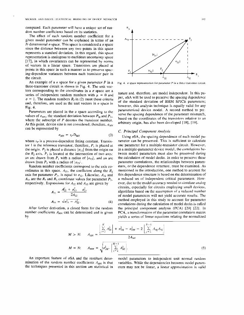
The effect of each random number coefficient for a given model parameter can be explained in terms of an N-dimensional U space. This space is considered a U space since the distance between any two points in this space represents a standard deviation. In this regard, this space representation is analogous to euclidean uncertainty space [17], in which covariances can be represented by norms of vectors in a linear space. Transistors are placed at points in this space in such a manner as to preserve spac- ing-dependent variances between each transistor pair in the circuit.
An example of a U space for a given parameter P in a three-transistor circuit is shown in Fig. 4. The unit vec- tors corresponding to the coordinates in a U space are a series of independent random numbers with p = 0 and U = 1 . The random numbers RI in (2) meet these criteria and, therefore, are used as the unit vectors in U space in Fig. 4.
Parameters are placed in the U space according to the values of U,,, the standard deviation between P , and P N , where the subscript of P denotes the transistor number. At this point, device size is not considered; therefore, U,,
can be represented by
UMN = SPDMN (3) where sp is a process-dependent fitting constant. Transis- tor 1 is the reference transistor; therefore, P I is placed at the origin. P2 is placed a distance I u ~ ~ ~ from the origin on the R2 axis. P , is located at the intersection of two arcs: an arc drawn from P I with a radius of 1 ~ 1 3 1 , and an arc drawn from P2 with a radius of 1 ~ ~ 3 1 .
Random number coefficients correspond to the axis co- ordinates in this space. A22, the coefficient along the R2 axis for parameter P 2 , is equal to u12. Likewise, A,, and A,, are the R2 and R3 coordinate values for parameter P, , respectively. Expressions for and are given by
A,, = a. (4) After further derivation, a closed form for the random
number coefficients AMN can be determined and is given by
R3 t
A22 A12
Fig. 4. o-space representation for parameter P in a three-transistor circuit.
nature and, therefore, are model independent. In this pa- per, USA will be used to preserve the spacing dependence of the standard deviation of BSIM SPICE parameters; however, this analysis technique is equally valid for any parameterized device model. A second method to pre- serve the spacing dependence of the parameter mismatch, based on the coordinates of the transistors relative to an arbitrary origin, has also been developed [ 181, [ 191.
C. Principal Component Analysis Using USA, the spacing dependence of each model pa-
rameter can be preserved. This is sufficient to calculate one parameter for a multiple-transistor circuit. However, in a multiple-parameter device model, the correlations be- tween model parameters must also be preserved during the calculation of model decks. In order to preserve these parameter correlations, the relationships between param- eters, or the dependence structure, must be examined. As mentioned in the introduction, one method to account for this dependence structure is based on the determination of a reduced set of independent critical parameters. How- ever, due to the model accuracy needed to simulate analog circuits, especially for circuits employing small devices, algorithms based on the assumption of a reduced number of model parameters will not yield accurate results. The method employed in this study to account for parameter correlations during the calculation of model decks is called the principal component analysis (PCA) [20]-[22]. In PCA, a transformation of the parameter correlation matrix yields a series of linear equations relating the normalized
r N i r N - I 1
An important feature of USA and the resultant deter- mination of the random number coefficients AMN is that the techniques presented in this section are statistical in
model parameters to independent unit normal random variables. While the dependencies between model param- eters may not be linear, a linear approximation is valid

158 IEEE JOURNAL OF SOLID-STATE CIRCUITS. VOL. 27. NO. 2 , FEBRUARY 1992
- VFB
K1 -
K2
ETA
MUZ
U0
- -
U1
X2M:
X2E
X3E
- -
x 2 u c
x 2 u 1 -
MUS
X2M!
X3M! -
X3U1
%w= -0.9011 1
-0.584:
0.6711
0.2461 -
0.1067
-0.094:
0.3439
-0.695:
-
-
-0.0884 0.1693 0.3231
0.0818 0.2384 0.3741 0.082C
0.0616 0.0144 -0.5006 0.2662
0.0349 0.4308 0.2981 0.5489
0.6302 0.5064 -0.5707 0.0561 I I I
-0.10431 0.19431 0.26571-0.39371 0.61751-0.35481 0.8254 I I I I I I
Fig. 5. Correlation matrix of BSIM SPICE model parameters for n-channel MOS transistors. Matrix is symmetrical
due to the small range over which parameter values vary (analogous to a small-signal approximation in analog cir- cuit analysis). PCA is applicable to the simulation of an- alog circuits, since no statistical information is lost due to parameter reduction assumptions. Additionally, PCA is a generalized statistical technique and is, therefore, valid for any model structure.
For the 2-pm n-well test chip, BSIM SPICE parameters were extracted from four chips, each containing 192 n-channel MOSFET's. Before finding parameter correla- tions, the extracted parameters were normalized. Nor- malization, necessary due to units considerations, is achieved as follows:
where p p and up are the population mean and standard deviation of parameter P , respectively, and P ' is the re- sultant normalized value for P. After normalization, pa- rameter correlations can be determined from
(7)
where ppQ is the correlation between parameters P and Q. The correlation matrix for the n-channel BSIM model as calculated from n-well test chip is presented in Fig. 5 .
Principal components can be related to the normalized parameters by determining the eigenvalues and eigenvec- tors of the correlation matrix and using the following equation :
(8)
where C is the principal component vector, A is the di- agonal matrix containing the eigenvalues of the parameter correlation matrix, U is the corresponding eigenvector
l N PPQ = igl J"
C = A-I/2U-Ip'
matrix, and P ' is the normalized parameter vector. Each principal component Ci is an independent normal random variable with zero mean and unit variance.
An added benefit of PCA is its ability to account for the variance of a device with many parameters by rela- tively few principal components. During PCA, the first principal axis, characterized by CI, is rotated in the nor- malized parameter space to align with the largest vari- ance. Further axis rotations are performed in a similar manner. Thus, the first few components will account for the majority of the total device variance. For the corre- lation matrix shown in Fig. 5 , the first six principal com- ponents, accounting for 96% of the total device variance, were retained.
Values for the normalized parameters can be calculated from the inverse of (8):
p ' = UA112C (9)
where the values for U and A have been previously de- termined. An example of the linear principal component equations is given in (10) for three important BSIM model parameters: the flat-band voltage (VFB), the linear region mobility ( M U Z ) , and the saturation region mobility ( M U S ) :
VFB' = O.6977Cl + 0.4067C2 - 0.4594C3
+ 0.089lC4 - 0.2610C5 + 0.1880C6
MUZ' = -0.0527C1 + 0.7673C2 - 0.0904C3
+ O.3323C4 + O.488OC5 + 0.1246C6
MUS' = O.6923Cl + 0.5491C2 - 0.3715C3
+ 0.0937C4 + 0. 1828C5 + 0.1525C6. (10)

MICHAEL A N D ISMAIL: STATISTICAL MODELING OF DEVICE MISMATCH I59
Values for C, can be randomly and independently gener- ated from a unit normal distribution ( p = 0, U = 1). Thus, for each transistor, six random variables are needed to calculate the 17 normalized parameters in the BSIM model. Through this method, values for the normalized parameters can be calculated quickly and easily. Repeated generation of the C vector constitutes a Monte Carlo ap- proach to sampling the multidimensional parameter space. If only a simple global variance is considered, these val- ues can be denormalized by inverting (6). The resultant parameter values can be entered into a simulator to deter- mine one output point. Repetition of this procedure will produce a variance for each circuit output. In this paper, denormalization is more complicated, as the parameter variances are dependent on both the device area and the separation distances between devices. However, the sam- pled normalized parameters will be invaluable in the cal- culation of model decks, since they are normally distrib- uted random variables which preserve the correlations between model parameters.
D. Model Integration
A combination of the models and algorithms examined in this section is necessary in order to calculate statisti- cally relevant model decks. Through USA, the device spacing dependence of the parameter standard deviation model is preserved. However, to fully realize the param- eter variance model given by ( l ) , a device area depen- dence must be included in the final model for parameter standard deviation. Likewise, the results of PCA must be integrated into this model in order to preserve the param- eter correlations inherent to the model. To calculate com- plete model decks, a model for the parameter means must also be included. An additional factor, the inter-die pa- rameter variance, should be inserted into the model to ac- count for wafer-level or wafer-to-wafer parameter vari- ance. While this component will not contribute to device mismatch, it will have an effect on circuit performance.
As previously noted, the result of entering random numbers for C, in the PCA-generated linear equations, shown in (lo), is a group of unit normal numbers that preserve the correlation between model parameters. If these normalized numbers are used in place of the unit normal random numbers in the USA, the result is a statis- tical model that preserves both the parameter correlations and the spacing dependency of the parameter variance. For example, the value for VFB ’ in (10) can be used as R2 in the uVFB equations similar to (2). Similarly, the value for MUZ’ in (10) can replace R, in the uMUz equation. Thus, the generation of six unit normal random numbers, C, . . C,, is capable of computing one model deck for one transistor. Each successive model deck is calculated by generating a new C, vector and calculating a new set of normalized parameters.
Statistical MOS (SMOS), a statistical model for a gen- eral parameter P of transistor M in an N-transistor circuit,
I
is given by I M
(1 1)
where p(PM) is the mean parameter value and RP are the correlated unit normal random numbers generated through PCA. While the statistical parameter model of (1 1) does not preserve parameter correlations exactly, the error in- troduced by incorporating PCA into the statistical model is negligible. For a typical circuit layout, calculated pa- rameter correlations deviate from their desired values by less than 1 %.
The model for the parameter means is based on the in- verse geometry dependence [12], [23] of SPICE param- eters. This model is generated by a least-squares fit to the 1 / L and 1 / Wfactors. The resultant equation for the mean parameter values is provided by
where L, and WM are, respectively, the length and width of transistor M, and p o p , p L p , and pwp are fitting con- stants. The uinter term represents the inter-die parameter variances, which can be modeled as a deviation in param- eter mean for each transistor in a circuit. In subsequent circuit simulations, the inter-die parameter variance terms are neglected. A complete set of fitting constants for the n-well test chip is provided in Table I.
111. EXPERIMENTAL AND SIMULATION This section contains a comparison between simulated
circuit variance using the statistical model described in Section I1 and experimental circuit variance determined from two test chips. Since a large number of any given circuit is necessary to confidently determine an actual variance, and since a limited amount of chip area is avail- able, two-transistor subcircuits are employed to test the algorithms.
A . Test Chip Description To test the statistical model presented in this paper, two
chip designs were fabricated from two different processes. A total of four chips from each design were obtained. Each of these chips contains sufficient test transistors to deter- mine both the parameter correlations and spacing-depen- dent parameter variances needed to characterize the sta- tistical model. In addition, each chip design includes numerous repetitions of a simple subcircuit whose actual output variance can be compared to a simulated variance.
Chip 1, fabricated using a MOSIS 2-pm p-well process, contains a total of 192 test transistors and 96 two-transis- tor grounded resistor circuits. The goal of this first chip is to test the algorithm which models the separation dis- tance dependence of the parameter standard deviation. As such, only two device sizes, W / L = 20/2 and 20/4 pm/pm, were fabricated. To test the distance depen-
I60 IEEE JOURNAL OF SOLID-STATE CIRCUITS. VOL. 27, NO. 2. FEBRUARY 1992
TABLE I
THE po TERMS. OTHER FITTING CONSTANTS HAVE UNITS AS DESCRIBED I N THE FINAL ROW. COMPLETE SET OF MODEL FITTING CONSTANTS FOR 2-pm N-WELL PROCESS. UNITS COLUMN REFERS TO
PO FL
VFB K1 K2 ETA MUZ U 0 U1 X2MZ X2E X3E x 2 u o x 2 u 1 MUS X2MS X3MS X3Ul TOX PHI VDD
-0.7923 1.063 1 0.1297
611.9 0.0478 0.2972
-0.0290
-3.063 -5.04E-3
3.93E-3 5.06E-4
763.5 -64.43
30.30 0.1502 0.0400 0.7500 5
-0.1009
0.1596
0.1116 0.0993 437.9 0.0764 0.7812
0.0269
- 0.3540
- 1.052
-5.43E-3 -6.93E-3
0.2365 1160 159.5 239.8 0 0 0 0
P W
-0.2149 0.6939 0.0565
-0.0321 - 107.5 -0.0632 -0.0720
104.5 -0.0172
0.0395 -0.1449 - 145.8
61.69 -26.61 - 3.38E-3
2.54E-4
0 0 0
J&
0.0623 0.0714 0.0178
27.9 6.25E-3 0.0714 4.545 8.89E-4 1.09E-3
5.41E-3
1.78E-3 0.0267 87.0 14.1 19.5 0.0194 0 0 0
SP
7.33E-5 4.53E-5 7.00E-6
0.0399 5.13E-6 4.67E-5 1.93E-3 6.67E-7
4.38E-6
4.30E-7 1.07E-6 6.2OE-6 0.0645 9.33E-4 0.0131 1.478-5 0 0 0
Units
V vn s
none none cm2/V . s V-‘ Pm/V cm2/VZ . s V - ’ V- ’ V-* V / V 2 cm2/V . s cm2/V2 . s cm’/V’ . s V / V 2 Fm V V
unit unit . pm unit . Fm unit . pm unit/pm
dence of the algorithm, M I and M 2 in the grounded re- sistor circuit [24], shown in Fig. 6, were separated by three different distances: 50, 100, and 150 pm. To save chip area, the M 1 transistors in the resistor circuits are also used as test transistors to determine parameter cor- relations and variances.
From the input node in Fig. 6 , the two transistor circuit fabricated on chip 1 acts as a grounded resistor with an equivalent resistance given by
L
The resistor circuit assumes identically sized MOSFET’s operating in the saturation region with a control voltage of V,. To achieve a linear resistance, this circuit depends on perfectly matched devices to cancel the nonlinearities inherent to the MOSFET. Thus, this circuit is a good can- didate to determine the effect of device mismatch on cir- cuit variance.
Chip 2, fabricated using a MOSIS 2-pm n-well process, also contains 192 test transistors and 96 two-transistor subcircuits. However, the subcircuit in this case is a sim- ple current mirror shown in Fig. 7. The contents and lay- out of one transistor group on the second test chip are
sistor groups are contained on the chip. As shown in Fig. 8 , three device sizes, W / L = 3/2 , 20/2, and 20/4 pm/pm, were included in this chip. Unlike the first test chip, the goal of chip 2 was to test the entire statistical model, including the area dependence of the parameter variance. Similar to the grounded resistors included in chip 1, M 1 and M 2 of the current mirrors were separated by three distances: 50, 100, and 150 pm as shown in Fig.
I I shown in Figs. 8 and 9, respectively. A total of 16 tran-
Voo= 5 v
v c q + I ; M2
- vc Fig. 6. Test circuit 1: two-transistor voltage-controlled all-MOS grounded
resistor.
I ss
vDD= 5 v
F5 0 I
- -
Fig. 7. Test circuit 2: current mirror
9. BSIM SPICE models were extracted from both of the current mirror transistors to determine the needed statis- tical data to characterize the statistical model. The off- chip load resistor was chosen to force the reference and mirrored currents to be equal. The same load resistor was then used for each measurement.

MICHAEL AND ISMAIL: STATISTICAL MODELING OF DEVICE MISMATCH 161
, L
,~ w - 20 I.Lm
4 Pm -
M12 M2 M9 M5
S
w - 20 Pm 2 Pm
M11 M7 MS M10
S
g@p-JF-U 2 pm M1 M3 M4 M6
S
Fig. 8. Contents of one transistor group on the second test chip.
50 pm
El E l m Fig. 9. Layout of one transistor group on the second test chip
The test structure consists of a column of test transis- tors, as shown in Figs. 9 and 10, for each device size examined. For each device size on the test chip, a total of 16 of these test columns are present, with each column oriented in the same direction. When calculating the mis- match of a given model parameter, a reference direction for the parameter difference is maintained. As an exam-
100 tun S m D = 5 0 p m
'1-'3
m t '2-'4
m t '1-'4
Fig. 10. Four-transistor column with available mismatch data.
ple, for a given transistor pair in Fig. 10, the parameter mismatch is always calculated by subtracting the param- eter value for the transistor which is physically lower in the figure from the parameter value for the physically higher transistor. Thus, the process variations character- ized by wafer-level gradients should affect each transistor pair separated by a certain distance in a similar fashion.
The advantage of maintaining a consistent direction of device separation during mismatch calculations is that the statistical model fitting constants can be determined in- dependently. The disadvantage of this scheme is that the parameter mismatch is measured in only one direction. Therefore, transistor columns similar to that shown in Fig. 10 should be oriented in at least two directions. However, sp can be approximated from these test chips by assuming that the measured parameter mismatch A P is equal to the standard deviation of A P , a(A P ) . Hence
A P = s p D (14)
where D is the separation distance between the transistor pair.
B. Parameter Extraction A BSIM parameter extractor, based on Berkeley's ex-
tractor [25] , was written specifically for this project. The extractor operates on an IBM PC or compatible computer and controls an HP4145B parameter analyzer. For this re- search, the primary issue for the BSIM parameter extrac- tor is the repeatability of the extractions. That is, if model parameters are repeatedly extracted from the same device, the parameters values should be consistent. To determine the repeatability of the parameter extractor, 16 BSIM parameters were extracted 25 times from the same device. Results of this experiment are presented in Table 11, where the parameter sensitivity is defined as the standard devia- tion of the extracted parameters. The repeatability of parameter extraction is slightly dependent on the device size; however, the parameter sensitivities for the device sizes investigated in this research were on the same order of magnitude. Most importantly, as long as the measured parameter-mismatch standard deviations are significantly larger than the parameter sensitivities listed in Table 11, the values determined for the statistical fitting constants are trustworthy.

I62
t PRINCIPAL COMPONENT
IEEE JOURNAL O F SOLID-STATE CIRCUITS. VOL. 27. NO. 2. FEBRUARY 1992
ANALYSIS - parameter correlations within transistor preserved
TABLE I1 REPEATABILITY OF EXTRACTED PARAMETERS FOR A
W / L = 2 0 / 2 - p m / p n DEVICE
7 CIRCUIT
DESCRIPTTON 0-SPACE ANALYSIS
~
Parameter Parameter Sensitivity Units
i - parameter variance between transistor preserved
RANDOM NUMBER
VFB K 1 K 2 ETA M U Z U 0 U 1 X 2 M Z X 2 E X3E x 2 u o x 2 u 1 MUS X 2 M S X 3 M S X 3 U 1
C- * device spacings
0.82E-3 0.73E-3 0.19E-3 0.16E-3 1 .1 0.07 IE-3 1 .OE-3 0.068 0 0.078E-3 0.049E-3 0.3 IE-3 1.2 0.30 0.625 0.68E-3
GENERATOR
V vo 5
none none cm2/V . s V-’ pm/V cmZ/V’ . s V-’ V- ’ v-2
pm/V’ cm2/V . s cm2/V2 . s cmZ/V2 . s V / V Z
C. Simulation A flowchart of the simulation procedure, including ex-
perimental and computational requirements for the actual model deck calculations, is presented in Fig. 11. The “Statistical Parameter Analysis” block constitutes the process characterization work which is necessary to de- termine the fitting constants in the statistical parameter models. This work must be performed only once for a given fabrication process. From the parameter correlation matrix, PCA will produce a series of linear equations re- lating the normalized parameters to a small number of in- dependent random numbers. These linear equations must also be calculated only once for a given process. Given a circuit description that includes device sizes and spac- ings, the random number coefficients A,, can be calcu- lated from ( 5 ) . If a circuit layout has not been completed, a nominal value can be entered for each separation dis- tance. Calculation of the random number coefficients must be performed only once for each circuit layout. There- fore, after the first model deck is calculated, only a few random numbers must be generated to calculate each suc- cessive model deck.
D. Results To test the modeling algorithms described in Section
11, SPICE model decks were calculated for both the resis- tor and the current mirror circuits for different device sizes and spacing using the statistical model. A total of 50 sim- ulations were performed on each circuit at each condition.
A comparison between simulated and actual means and standard deviations for the grounded resistor circuit with device sizes of 20/2 and 20/4 pm/pm is provided in Table 111. The simulated and actual mean resistances at each control voltage show excellent agreement. This agreement is expected since the statistical data base from which the simulation is derived is based, in part, on pa- rameter extractions of the transistors in the actual resistor circuits. The agreement between simulated and actual
STATISTICAL PARAMETER ANALYSIS
1 1
I CIRCUlT I MODEL INTEGRATION
* model decks calculated using statistical model
* sufficient for one circuit simulation
CIRCUIT SIMULATION + CIRCUlT OUTPUT
VARIANCES
Fig. 11. Simulation flowchart.
mean resistances is, therefore, an indication that the BSIM parameter extraction program is accurate. In general, the simulated and actual mean resistances will not be equal due to inter-die process variations. However, inclusion of the inter-die parameter variance term in (12) should ac- count for these variations. The trend of increasing circuit output standard deviation as separation distance between devices is increased is clearly shown in both the simula- tion and experimental data. Simulation results using the die-level parameter standard deviations, the standard de- viation of a parameter over an entire die, are presented to compare the new statistical model with previous models. Simulations using die-level standard deviations tend to be overly pessimistic for small circuits and yield no infor- mation concerning the effect of circuit layout on output variance.
Similar to the density histogram of flat-band voltage mismatch presented in Fig. I , the distribution of current mismatch for the current mirrors of the second test chip is plotted in Fig. 12. Once again, the reference MOSFET in the mirror is always kept toward one side of the wafer. Through this measurement technique, the two mismatch causing effects can be separated. The variation about the mean current difference is due to the random area de- pendence of the statistical parameter model. The non- zero mean current difference is caused by the nonrandom separation distance dependence of the parameter

MICHAEL A N D ISMAIL: STATISTICAL MODELING OF DEVICE MISMATCH
U 0 0
o 088888308 I I I I
I63
0 0 883300 AI
TABLE 111 MEASURED A N D SIMULATED VALUES FOR RESISTANCE MEAN A N D STANDARD DEVIATION A T THREE
DIFFERENT CONTROL VOLTAGES FOR W / L = 20/2- A N D 20/4-pm/pm DEVICES. ALL RESISTANCE VALUES A R E I N OHMS.
W / L = 20/2 p / p m
Statistic Bias Measured Simulated Measured Simulated
W / L = 20/4 pm/pm
~~
v c = 2 v 905 910 2137 2141 Mean v c = 3 v 726 720 1398 1405
v c = 4 v 688 692 1200 1207
D = 50-pm v c = 2 v 8.8 9.0 8.5 7.5 Standard v c = 3 v 7.6 8.0 6.4 5.5 Deviation v c = 4 v 6.2 6.6 5.5 4.5
D = 100-pm v c = 2 v 11.6 12.3 10.2 9.8 Standard v c = 3 v 8.7 9.9 8.0 6.9 Deviation v c = 4 v 7.4 7.6 6.2 5.4
D = 150-pm v c = 2 v 12.4 12.7 10.9 10.5 Standard v c = 3 v 10.8 10.4 9.6 8.8 Deviation v c = 4 v 8.5 7.8 7.9 6.8
Die-Level v c = 2 v 16.3 16.9 15.4 15.0 Standard v c = 3 v 10.4 11 .1 11.3 9.9 Deviation v c = 4 v 8.7 9.0 8.0 7.1
MEAN = 0.23 pA
D = 5 0 y m Standard Deviation = 0.325 pA 0 0
I I I I I I I I I 1 I AI - 1 pA -0.5 pA 0 0.5 pA 1pA 1.5 pA
MEAN = 0.45 pA
D = 100 pn StandardDeviation =0.310 I I I I I I I I I I I I AI
-1 pA -0.5 pA 0 0.5 pA 1pA 1.5 PA
MEAN = 0.74 pA
D = 150 pm Standard Deviation = 0.340 p,4
-1 pA -0.5 pA 0 0.5 pA 1pA 1.5 pA
Fig. 12. Mismatch in mirrored current for W / L = 20/4-pm/pm devices at three different device separation distances. Reference current is 50 wA.
variance model. Table IV includes simulated and experi- mental standard deviations for the current mirrors fabri- cated on chip 2. As shown in this table, the SMOS model is capable of preserving the device area, circuit layout, and bias dependencies of transistor mismatch when in- corporated in a circuit simulator.
The measured and simulated values for the standard de-
viation of mirrored current show good agreement. As ex- pected, the relative effect of the separation distance be- tween devices on the standard deviation increases as devices size increases. The dependence of device area on the standard deviation is also evident, although the differ- ence in bias conditions due to the different W / L ratios distorts the 1 / C L dependence.
Statistical simulation results, shown in Figs. 13 and 14, for the current mirror circuit with constant current bias illustrate the dependencies of device area, separation dis- tance, and bias on the current mismatch variance. Each simulation point on these graphs corresponds to 1000 Monte Carlo simulations using a CAD implementation of the SMOS model [19], [26]. Fig. 13 shows the impor- tance of circuit layout and device size on circuit perform- ance variance. Fig. 14 investigates the effect of bias, with the result that small V,, - V , values (small Is,) cause greater relative mismatch. Of course, the design of the bias point may be constrained by circuit performance re- quirements. It is important, however, for analog design- ers to be aware of the relative effect of transistor bias, as well as the device size and placement, on the reliability of circuit performance.
IV. DISCUSSION Accounting for the effects of transistor separation dis-
tance and device size in the statistical model allows the simulation of circuits based on circuit layout and critical dimension. A byproduct of statistical modeling based on intra-die statistics is the possibility of optimizing the cir- cuit layout or the device sizes. With a simulation tool based on this statistical model, accurate simulations of analog circuits can be performed in which the circuit per- formance is correlated to input parameter spread. This will

164 IEEE JOURNAL O F SOLID-STATE CIRCUITS. VOL. 27. NO. 2. FEBRUARY 1992
TABLE IV
Two DIFFERENT REFERENCE CURRENTS. ALL CURRENT VALUES A R E I N MICROAMPERES MEASURED A N D SIMULATED VALUES FOR MEAN A N D STANDARD DEVIATION OF MIRRORED CURRENT FOR
W / L = 3/2 pm/pm W / L = 20/2 pm/pm W / L = 20/4 pm/pm
Statistic Bias Measured Simulated Measured Simulated Measured Simulated
Mean 5 0 p A 50.05 49.98 49.90 50.05 50.15 49.94 100pA 100.13 99.86 99.92 100.02 99.88 99.92
D = 50-pm 5 0 p A 0.815 0.828 0.642 0.647 0.407 0.390 Standard 100 p A 1.462 1.477 1.080 0.990 0.519 0.667 Deviation
D = 100-pm 5 0 p A 0.824 0.843 0.708 0.843 0.577 0.537 Standard 100 p A 1.476 1.538 1.196 1.252 0.850 0.848 Deviation
D = 150-pm 50 pA 0.857 0.845 0.857 1.180 0.808 0.752 Standard 100 p A 1.552 1.596 1.427 1.711 1.141 I . 140 Deviation
0 D=minimum - D=sopIl - D=lOopIl 1.5 -m- D = l 5 0 ~
1.0 -
0.5 - 0 0
0.0 ' 1 . 1 ' ' ' 1 ' 1 . I 0 100 200 300 400 500 600 700
AREA ( p m 2 ) Fig. 13. Simulated device area and separation distance dependence of cur- rent mirror circuit. All simulations performed at I,, = 50 pA and W / L =
1.5.
2.0
1.5
1.0
0.5
0.0 -1 0 5 10 15 20 25
"/L Fig. 14. Simulated bias dependence of current mirror circuit. All simula- tions performed for device areas of 80 pmZ and at minimum separation distances.
as the CAD aspects of this research will be explored in a later paper [26].
An important feature of the primary algorithms used to model device mismatch in this study, USA and PCA, is that both algorithms are statistical in nature and, there- fore, independent of model or technology. The BSIM SPICE model was chosen in this study due to its ability to accurately model short-channel transistors; however, any parameterized device model could have been used. Similarly, this study focused on the dc parameters in the BSIM model, but the model deck calculation procedures are equally valid for any model parameters including par- asitic capacitances. Since model parameters are extracted from both the linear and saturation regions, the statistical model is valid for transistors operating in either region.
When formulating this or any statistical model, a large and accurate data base is necessary to characterize the process. In a production environment, an adequate data base can be amassed through extraction of model param- eters from simple test structures, consisting of n- and p-channel transistors spaced at different intervals. Our statistical data base was extracted from two test chips fab- ricated through MOSIS. Since area was limited on these chips, the statistical data needed to model and simulate MOS transistors were gathered for n-channel devices only. Inclusion of p-channel devices into the statistical model is a simple extension of the modeling scheme presented in this paper. The mismatch, or intra-die, components of the statistical model can be assumed independent for n- and p-channel MOSFET's. For the inter-die variations, correlations between n-channel and p-channel model pa- rameters can be determined and entered into an expanded correlation matrix. Thus, through PCA, parameter cor- relations for each device type on the die can be preserved.
enable the circuit designer to determine which transistors in the circuit contribute most to the output variance. Thus, the minimum device size for which the circuit will meet specifications or the circuit layout which minimizes mis- match-induced variance can be determined. A more de- tailed explanation of circuit optimization methods as well
V. CONCLUSION As device feature sizes in analog circuits are reduced
to the micrometer or submicrometer range, the effect of device mismatch on circuit performance and reliability

MICHAEL A N D ISMAIL: STATISTICAL MODELING OF DEVICE MISMATCH 165
will be magnified. Statistical methods are required to sim- ulate mismatch induced variance; therefore, an accurate statistical device model is required. This paper describes the SMOS model, a statistical parameter-level MOS model, from which statistically significant device model decks can be calculated.
The SMOS model is derived from the underlying mis- match variance model which contains the dependence of parameter variance on device size and spacing. Two sta- tistical algorithms, principal component analysis and a-space analysis, are employed to preserve parameter cor- relations within a transistor and parameter variances be- tween transistors, respectively. The two statistical algo- rithms are integrated with the mismatch variance model to create a unified CAD-compatible statistical model for MOS transistors. The ability of the SMOS model to sim- ulate circuit output variances based on intra-die statistics has been verified through experimental data gathered from two test chips. Simulated and measured circuit output variances and distributions showed excellent agreement.
Integration of this statistical model into a CAD envi- ronment will allow the analog circuit designer to estimate circuit yield based on a given set of processing-dependent model fitting parameters. Due to the ability of this model to accurately simulate the effect of device size and sepa- ration distance between devices on circuit output vari- ances, we believe that this model can be an integral part of a circuit optimization scheme [27] which includes both device size and layout optimization. It is also possible that the SMOS model could be integrated into an automated circuit layout [28] or synthesis [29] environment to design circuits which meet yield requirements. Worst-case anal- ysis [30] of analog MOS integrated circuits could also benefit from the SMOS model due to its ability to accu- rately model the effects of device mismatch.
REFERENCES [ I ] J.-B. Shyu, G . C. Temes, and F. Krummenacher, “Random error
effects in matched MOS capacitors and current sources,” IEEE J . Solid-state Circuits, vol. SC-19, pp. 948-955, Dec. 1984.
[2] K. R. Lakshmikumar, R. A. Hadaway, and M. A. Copeland, “Char- acterization and modeling of mismatch in MOS transistors for preci- sion analog design,” IEEE J . Solid-State Circuits, vol. SC-21, pp, 1057-1066, Dec. 1986.
[3] M. J. M. Pelgrom, A. C. J . Duinmaiger, and A . P. G. Welbers, “Matching properties of MOS transistors,” IEEE J . Solid-state Cir- cuits, vol. 24, pp. 1433-1439, Oct. 1989.
[4] P. Cox, P. Yang, S . S . Mahant-Shetti, and P. Chatterjee. “Statistical modeling for efficient parametric yield estimation of MOS VLSI cir- cuits,” IEEE J . Solid-State Circuits, vol. SC-20, pp. 391-398, Feb. 1985.
[5] T.-K. Yu, S . M. Kang, I. N. Hajj, and T. N. Trick. “Statistical performance modeling and parametric yield estimation of MOS VLSI,” IEEE Trans. Computer-Aided Design, vol. CAD-6, pp. 1013- 1022, Nov. 1987.
[6] D. E. Hocevar, P. F. Cox, and P. Yang, “Parametric yield optimi- zation for MOS circuit blocks,” IEEE Trans. Computer-Aided De- sign, vol. 7 , pp. 645-658, June 1988.
[7] J. P. Spoto, W . T. Coston, and C. P. Hernandez, “Statistical inte- grated circuit Design and Characterization,” IEEE Trans. Computer- Aided Design, vol. CAD-5, pp. 90-103, Jan. 1986.
[8] S . Inohira, T . Shinmi, M. Nagata, T. Toyabe, and K. Iida, “A sta- tistical model including parameter matching for analog integrated cir- cuits simulation,” IEEE Trans. Electron Devices, vol. ED-32, pp. 2177-2184, Oct. 1985.
[9] N . Herr and J. J. Barnes, “Statistical circuit simulation modeling of CMOS VLSI,” IEEE Trans. Computer-Aided Design, vol. CAD-5, pp. 15-22, Jan. 1986.
[IO] C. K. Chow, “Projection of circuit performance distributions by mul- tivariate statistics,” IEEE Trans. Semicond. Manuf. vol. 2, pp. 60- 65, May 1989.
1111 E. D. Boskin and C. J. Spanos, “Worst case device characterization for statistical circuit design,” in Proc. SRC TECHCON, 1990, pp. 165-168.
[I21 B. J. Sheu, D. L. Scharfetter, P.-K. KO, and M.-C. Jeng, “BSIM: Berkeley short-channel IGFET model for MOS transistors,” IEEE J . Solid-state Circuits, vol. SC-22, pp. 558-566, Aug. 1987.
[I31 T. Quarles, A. R. Newton, D. 0. Pederson, and A. Sangiovanni- Vincentelli. “SPICE 3B1 user’s guide,” Electron. Res. Lab., Univ. Calif., Berkeley, Apr. 1987.
[I41 J. M. Cassard. “A sensitivity analysis of SPICE parameters using an eleven-stage ring oscillator,’’ IEEE J . Solid-State Circuits, vol. SC- 19, pp. 130-135, Feb. 1984.
[I51 G. Troster and P. Tomaszewsli. “Mismatch simulation for layout sensitive parameters of IC components and devices,” IEEE Trans. Computer-Aided Design, vol. 8, pp. 101-107, Feb. 1989.
[I61 C. Michael and M. Ismail, “Simulation of mismatch induced vari- ance in short-channel analog CMOS circuits,” in Proc. SRC TECH- CON, 1990, pp. 351-354.
[I71 Ove Ditlevsen, Uncertainty Modeling. New York: McGraw-Hill Inc., 1981.
[I81 C. Michael, C. Abel, and M. Ismail, “SMOS: A CAD-compatible statistical model for analog MOS integrated circuit simulation,” to be published in Int. J . Circuit Theory and Applications.
[I91 C. Michael, “Statistical modeling for computer-aided design of an- alog MOS integrated circuits,” Ph.D. dissertation, Ohio State Univ., Columbus, 1991.
[20] B. Flury, Common Principal Components and Related Multivariate Models. New York: Wiley, 1988.
[21] E. E. Cureton and R. B. D’Agostino, Factor Analysis; An Applied Approach.
[22] A. A. Afifi and S . P. Azen, Statistical Analysis: A Computer Oriented Approach. New York: Academic, 1972.
[23] M. C. Hsu and B. J . Sheu. “Inverse-geometry dependence of MOS transistor electrical properties,” IEEE Trans. Computer-Aided De- sign, vol. CAD-6, pp. 582-585, July 1987.
[24] M. Ismail, “CAD-compatible analog system design: A new design concept,” Introduction to Analog VLSI Design Automation, M . Is- mail and J . Franca, Eds. Boston: Kluwer Academic 1989, ch. 7, pp. 163-181.
[25] M.-C. Jeng, B. J . Sheu, and P. K. KO, “BSIM parameterextraction- Algorithms and user’s guide,” Univ. Calif., Berkeley, UCBIERL M85/79, 1985.
[26] C. Michael, A. Kankkunen, M. Valtonen, and M. Ismail, “Statistical computer-aided design and optimization of analog MOS integrated circuits,” to be published in IEEE Trans. Computer-Aided Design.
[27] C. Michael and M. Ismail, Statistical Modeling for Computer-Aided Design of MOS VLSI Circuits. Boston: Kluwer Academic, 1992 (to be published).
[28] J. M. Cohn, D. J. Garrod, R. A. Rutenbar, and L. R. Carley, “KOANIANAGRAM 11: New tools for device-level analog place- ment and routing,” IEEE. J . Solid-State Circuits, vol. 26, pp. 330- 342, Mar. 1991.
[29] R. Harjani, R. A. Rutenbar, and L. R. Carley, “OASYS: A frame- work for analog circuit synthesis,” IEEE Trans. Computer-Aided De- sign, vol. 8, pp. 1247-1266, Dec. 1989.
[30] S. R. Nassif, A. J. Strojwas, and S . W. Director, “A methodology for worst-case analysis of integrated circuits,” IEEE Trans. Com- puter-Aided Design, vol. CAD-5, pp. 104-1 13, Jan. 1986.
Hillsdale, NJ: Lawrence Erlbaum Associates, 1983.
Christopher Michael was born in State College, PA, in 1964. He received the B.S., M.S., and Ph.D. degrees in electrical engineering from Ohio State University, Columbus, in 1986, 1988, and 1991, respectively. His dissertation work focused on statistical modeling and simulation for com- puter-aided design of analog MOS integrated cir- cuits.
He was employed by Texas Instruments Incor- porated, Dallas, TX, during the summers of 1989 and 1990, where he worked on fabrication equip-

I66 IEEE JOURNAL OF SOLID-STATE CIRCUITS. VOL. 27. NO. 2 . FEBRUARY 1992
ment modeling for process control. In 1991, he joined National Semicon- ductor Corporation, Santa Clara, CA, as a Senior Process Engineer. His primary responsibilities include device characterization and process inte- gration for a mixed analogldigital process.
Dr. Michael was the recipient of a University Fellowship, a DuPont Graduate Fellowship, and a DuPont Teaching Fellowship while at Ohio State University.
Mohammed Ismail (S’80-M’82-SM’84) re- ceived the B.S. and M.S. degrees from Cairo Uni- versity and the Ph.D. degree from the University of Manitoba in 1983, all in electrical engineering.
He has held several positions in industry and academia in the U.S., Canada, and overseas. He is currently with the Solid-state Microelectronics Laboratory at Ohio State University, Columbus, as an Associate Professor of Electrical Engineer- .ing. His current interests are in the areas of ana- log/digital VLSI design in CMOS/BiCMOS,
CAD-compatible analog IC design, statistical modeling and simulation of device mismatch in VLSl circuits, and artificial neural information pro- cessing.
Dr. Ismail was an Associate Editor of the IEEE TRANSACTIONS ON CIR- CUITS AND SYSTEMS, 1989-1991, and of the IEEE Circuits and Devices Magazine, 1988-1990, and is currently the CAS Editor of the magazine. He is the founder and Editor-in-chief of Analog Integrated Circuits and Signal Processing, a new intemational joumal. He is the Editor of the Klu- wer Book Series on Analog Circuits and Signal Processing. He served on several technical committees and was the chairman of the IEEE Circuits and Systems (CAS) Society’s Technical Committee on Analog Signal Pro- cessing (1987-1990) and the General Chairman of the 29th Midwest Sym- posium on Circuits and Systems (1986). He has published about 80 tech- nical papers and co-edited and coauthored two books: Analog VLSI Implementation of Neural Systems and Introduction to Analog VLSl Design Automation. He is listed in American Men and Women of Science and in Who’s Who in Technology. He has given numerous invited lectures and organized and chaired technical sessions, workshops, short courses and panel discussions at many international meetings. He has received several research and teaching awards including the U.S. National Science Foun- dation Presidential Young Investigator Award.
Related Documents


