State Transition Diagram for A Pipeline Unit based on Single Electron Tunneling Anup Kumar Biswas Assistant Professor Department of Computer Science and Engineering Kalyani Govt. Engineering College Kalyani-741235, Nadia, West Bengal, India, Abstract:- For low cost, low power consumption, high operating speed, and high integration density-based electronic goods are economically indispensable in business, engineering, science and technology in the present era. Single Electron tunneling is one such approach by which all the logic gates can be implemented. Single Electron tunneling devices (SEDs) and Linear Threshold Gates (LTGs) have the capabilities of controlling the transport of only an electron through a tunnel junction. A single electron which has the charge sufficient to store information in a SED in the atmosphere of 0K. Power being consumed in the single electron tunneling circuits is very low comparing the (CMOS) circuits. The speed of the processing of LTG based device will be very close to electronic speed. The single-electron transistor (SET) and LTG both attract the scientists, technologists and researchers to design and implement their large scale circuits for small cost of the ultra-low power and its small size. All the tunneling events in the case of a LTG-based circuit happen when only a single electron tunnels from one conductor to other through the tunnel junction under the proper applied bias voltage and multiple input voltages. For implementing a state transition diagram for a pipeline unit, LTG would be a best candidate to fulfill the necessities requiring for its implementation. As far as Ultra-low noise is concerned, LTG based circuit would be a best selection for implementing the desired tunneling circuits. Different LTGs, a D-Flip-flop, a 2:1 multiplexer are implemented, and above all, a state transition circuit for a pipeline is implemented also. Key words: State transition, Electron-tunneling, Coulomb- blockade, pipeline, linear threshold gate 1. INTRODUCTION We are interested in constructing a state transition diagram for a pipeline unit which can provide us with collision or collision free transition for latency m ( m is an integer number). Our intention for doing so is to utilize the electron tunneling phenomena through the SET as there is very ultra- low power being consumed for a single electron while tunneling. For the purpose of the implementing of a state transition diagram circuit, one can take advantages of SET and other one can take that of LTG. In the present situation we will accept the second case i.e. using LTG a state transition diagram will be presented. The logic gates required to construct “State transition diagram for a pipeline unit” are being OR, AND, NAND. In addition to them (i) combinational circuits like 2:1 multiplexers and (ii) sequential circuits like D Flip-flops will be necessary. All of them will be described step by step and their comparative studies will be shown in due places. 2. TUNNEL JUNCTION AND SINGLE ELECTRON TRANSISTOR A tunnel junction is made up of two conducting materials and a thin insulating barrier between them. The tunnel junction must have a capacitance C and a resistance . The conducting electrodes of the tunnel junction will be a superconducting or semiconducting material. When we are considering them as superconducting, electron(s) having one elementary charge (1.60217662 × 10 -19 Coulombs) carry the current through the junction. We have the knowledge that current can’t flow through the insulating barrier as it creates a barrier against the movement of an electron in the case of classical electrodynamics, whereas for the case of quantum mechanics, there must be a positive possibility that when an electron residing in one side of the barrier of the insulator in order to reach the another side of it, the electron to which the bias or input voltages are supplied can go to the other electrode. If bias voltage greater than the threshold voltage is applied properly, there will be a current flow. Avoiding other effects, the current will be following in proportion to the bias voltage applied as per the first-order–approximation-tunneling process. In electrical terms, a tunnel junction, of course, have a constant resistance R value relying on its barrier thickness a shown in Fig 1(a). When the two conducting materials are connected with an insulating layer between them together, there will also have a capacitance in the junction. In this context, the insulator represents itself as dielectric and two conducting plates with dielectric forms a capacitor C in the tunnel junction. For the discrete nature of electric charge in the tunneling phenomenon, current following through a tunnel junction is discontinuous i.e., a series of events in which merely one electron will be able to pass or tunnel through the tunnel junction at a particular time. Owing to the single electron tunneling through the junction, the tunnel capacitance is charged with an elementary charge (1.60217662 × 10 - 19 Coulombs) developed a voltage according to the relation = , where C=tunnel junction capacitance. When the capacitance of the tunnel junction is ultra-small in order of O(10 −18 ) , the voltage building up in the tunnel junction will be adequate to prevent another electron(s) to tunnel through. We will be able to suppress electrical current when the bias voltage being applied is lower than the voltage created in the tunnel junction, as a result, the resistance of the device will no longer remain constant. The increment of the differential resistance of the tunnel junction around zero bias is said to be the Coulomb blockade [1, 10, 13, 15]. International Journal of Engineering Research & Technology (IJERT) ISSN: 2278-0181 http://www.ijert.org IJERTV10IS040205 (This work is licensed under a Creative Commons Attribution 4.0 International License.) Published by : www.ijert.org Vol. 10 Issue 04, April-2021 325

Welcome message from author
This document is posted to help you gain knowledge. Please leave a comment to let me know what you think about it! Share it to your friends and learn new things together.
Transcript
State Transition Diagram for A Pipeline Unit
based on Single Electron Tunneling
Anup Kumar Biswas Assistant Professor
Department of Computer Science and Engineering
Kalyani Govt. Engineering College
Kalyani-741235, Nadia, West Bengal, India,
Abstract:- For low cost, low power consumption, high operating
speed, and high integration density-based electronic goods are
economically indispensable in business, engineering, science
and technology in the present era. Single Electron tunneling is
one such approach by which all the logic gates can be
implemented. Single Electron tunneling devices (SEDs) and
Linear Threshold Gates (LTGs) have the capabilities of
controlling the transport of only an electron through a tunnel
junction. A single electron which has the charge sufficient to
store information in a SED in the atmosphere of 0K. Power
being consumed in the single electron tunneling circuits is very
low comparing the (CMOS) circuits. The speed of the
processing of LTG based device will be very close to electronic
speed. The single-electron transistor (SET) and LTG both
attract the scientists, technologists and researchers to design
and implement their large scale circuits for small cost of the
ultra-low power and its small size. All the tunneling events in
the case of a LTG-based circuit happen when only a single
electron tunnels from one conductor to other through the
tunnel junction under the proper applied bias voltage and
multiple input voltages. For implementing a state transition
diagram for a pipeline unit, LTG would be a best candidate to
fulfill the necessities requiring for its implementation. As far as
Ultra-low noise is concerned, LTG based circuit would be a
best selection for implementing the desired tunneling circuits.
Different LTGs, a D-Flip-flop, a 2:1 multiplexer are
implemented, and above all, a state transition circuit for a
pipeline is implemented also.
Key words: State transition, Electron-tunneling, Coulomb-
blockade, pipeline, linear threshold gate
1. INTRODUCTION
We are interested in constructing a state transition diagram
for a pipeline unit which can provide us with collision or
collision free transition for latency m ( m is an integer
number). Our intention for doing so is to utilize the electron
tunneling phenomena through the SET as there is very ultra-
low power being consumed for a single electron while
tunneling. For the purpose of the implementing of a state
transition diagram circuit, one can take advantages of SET
and other one can take that of LTG. In the present situation
we will accept the second case i.e. using LTG a state
transition diagram will be presented. The logic gates
required to construct “State transition diagram for a pipeline
unit” are being OR, AND, NAND. In addition to them (i)
combinational circuits like 2:1 multiplexers and (ii)
sequential circuits like D Flip-flops will be necessary. All of
them will be described step by step and their comparative
studies will be shown in due places.
2. TUNNEL JUNCTION AND SINGLE ELECTRON
TRANSISTOR
A tunnel junction is made up of two conducting materials
and a thin insulating barrier between them. The tunnel
junction must have a capacitance C and a resistance 𝑅𝑡. The
conducting electrodes of the tunnel junction will be a
superconducting or semiconducting material. When we are
considering them as superconducting, electron(s) having one
elementary charge (1.60217662 × 10⁻¹⁹ Coulombs) carry the
current through the junction.
We have the knowledge that current can’t flow through the
insulating barrier as it creates a barrier against the movement
of an electron in the case of classical electrodynamics,
whereas for the case of quantum mechanics, there must be a
positive possibility that when an electron residing in one side
of the barrier of the insulator in order to reach the another
side of it, the electron to which the bias or input voltages are
supplied can go to the other electrode. If bias voltage greater
than the threshold voltage is applied properly, there will be
a current flow. Avoiding other effects, the current will be
following in proportion to the bias voltage applied as per the
first-order–approximation-tunneling process. In electrical
terms, a tunnel junction, of course, have a constant resistance
R value relying on its barrier thickness a shown in Fig 1(a).
When the two conducting materials are connected with an
insulating layer between them together, there will also have
a capacitance in the junction. In this context, the insulator
represents itself as dielectric and two conducting plates with
dielectric forms a capacitor C in the tunnel junction. For the
discrete nature of electric charge in the tunneling
phenomenon, current following through a tunnel junction is
discontinuous i.e., a series of events in which merely one
electron will be able to pass or tunnel through the tunnel
junction at a particular time. Owing to the single electron
tunneling through the junction, the tunnel capacitance is
charged with an elementary charge (1.60217662 × 10-
19 Coulombs) developed a voltage according to the relation
𝑉 =𝑒
𝐶 , where C=tunnel junction capacitance. When the
capacitance of the tunnel junction is ultra-small in order of
O(10−18) , the voltage building up in the tunnel junction will
be adequate to prevent another electron(s) to tunnel through.
We will be able to suppress electrical current when the bias
voltage being applied is lower than the voltage created in the
tunnel junction, as a result, the resistance of the device will
no longer remain constant. The increment of the differential
resistance of the tunnel junction around zero bias is said to
be the Coulomb blockade [1, 10, 13, 15].
International Journal of Engineering Research & Technology (IJERT)
ISSN: 2278-0181http://www.ijert.org
IJERTV10IS040205(This work is licensed under a Creative Commons Attribution 4.0 International License.)
Published by :
www.ijert.org
Vol. 10 Issue 04, April-2021
325
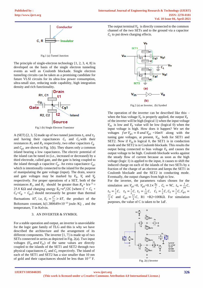
Fig.1 (a) Tunnel Junction
The principle of single-electron technology [1, 2, 3, 4, 8] is
developed on the basis of the single electron tunneling
events as well as Coulomb blockade. Single electron
tunneling circuits can be taken as a promising candidate for
future VLSI circuits for its ultra-low power consumption,
ultra-small size, reducing node capability, high integration
density and rich functionality.
Fig.1 (b) Single Electron Transistor
A (SET) [2, 3, 5] made up of two tunnel junctions 𝑡1 𝑎𝑛𝑑 𝑡2
and having their capacitances 𝐶1 and 𝐶2 with their
resistances 𝑅1 and 𝑅2 respectively, two other capacitors 𝐶𝑔
and 𝐶𝑔1 are shown in Fig. 1(b). They shares only a common
inland bearing a low capacitance. The electric potential of
the island can be tuned in (i.e., increased or decreased) by a
third electrode, called gate, and the gate is being coupled to
the island through a capacitor 𝐶𝑔. An extra capacitance 𝐶𝑔1
which is intentionally connected to the island for the purpose
of manipulating the gate voltage (input). The drain, source
and gate voltages may be marked by 𝑉𝑏, 𝑉𝑠 and 𝑉𝑔
respectively. For proper operations of a SET, both of the
resistances 𝑅1, and 𝑅2 should be greater than 𝑅𝑞= h/𝑒 2 ≈
25.8 KΩ and charging energy EC=e2/2C [where 𝐶 = 𝐶1 +
𝐶2+𝐶𝑔 + 𝐶𝑔1] should necessarily be greater than thermal
fluctuations 𝑘𝑇, i.e, 𝐸𝐶 =𝑒2
2𝐶> 𝑘𝑇, the product of the
Boltzmann constant, k(1.380649×10⁻²³ joule /K) , and the
temperature, T in Kelvin.
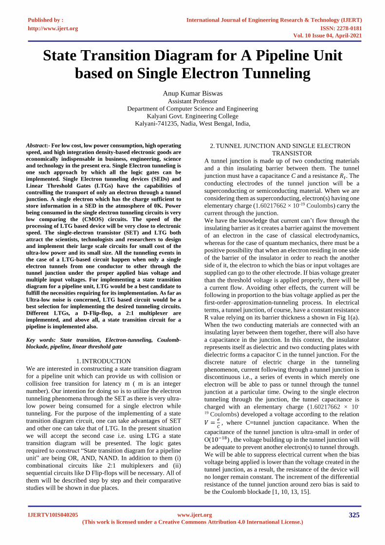
3. AN INVERTER & SYMBOL
For a stable operation and output, an inverter is unavoidable
for the logic gate family of TLG and this is why we have
described the architecture and the arrangement of its
different components. The inverter [1, 7] is made up of two
SETs connected in series as depicted in Fig. 2(a). Two input
voltages (𝑉𝑖𝑛 𝑎𝑛𝑑 𝑉𝑖𝑛) of the same values are directly
coupled to the islands of the SET1 and SET2 through two
physical capacitances 𝐶1 and 𝐶2 respectively. The island of
each of the SET1 and SET2 has a size smaller than 10 nm
of gold and their capacitances should be less than 10-17 F.
The output terminal 𝑉0 is directly connected to the common
channel of the two SETs and to the ground via a capacitor
𝐶𝐿 to put down charging effects.
Fig.2 (a) an Inverter, (b) Symbol
The operation of the inverter can be described like this: -
when the bias voltage 𝑉𝑏 is properly applied, the output 𝑉0 of the inverter will be high (logical 1) when the input voltage
𝑉𝑖𝑛 is low and 𝑉0 value will be low (logical 0) when the
input voltage is high. How does it happen? We set the
voltages 𝑓𝑜𝑟 𝑉𝑔1 = 0 𝑎𝑛𝑑 𝑉𝑔2 =16mV along with the
tuning gate voltages, at present, 𝑉𝑖𝑛 both for SET1 and
SET2. Now if 𝑉𝑖𝑛 is logical 0, the SET1 is in conduction
mode and the SET2 is in Coulomb blockade. This results the
output being connected to bias voltage 𝑉𝑏 and causes the
output voltage to be high. Coulomb blockade works against
the steady flow of current because as soon as the high
voltage (logic 1) is applied to the input, it causes to shift the
induced charge on each of the islands of the two SETs by a
fraction of the charge of an electron and keeps the SET1 in
Coulomb blockade and the SET2 in conducting mode.
Eventually, the output changes from high to low.
For the inverter, the parameters values chosen for the
simulation are: 𝑉𝑔1=0, 𝑉𝑔2=0.1×𝑞𝑒
𝐶 , 𝐶𝐿 = 9𝐶, 𝑡4 =
1
10𝐶,
𝑡3 =1
2𝐶, 𝑡2 =
1
2𝐶, 𝑡1 =
1
10𝐶, 𝐶1 =
1
2𝐶, 𝐶2 =
1
2𝐶, 𝐶𝑔1 =
17
4𝐶 and 𝐶𝑔2 =
17
4𝐶, R1 =R2=100KΩ. For simulation
purposes, the value of C is taken to be 1aF.
Fig. 2(c) Inverter
International Journal of Engineering Research & Technology (IJERT)
ISSN: 2278-0181http://www.ijert.org
IJERTV10IS040205(This work is licensed under a Creative Commons Attribution 4.0 International License.)
Published by :
www.ijert.org
Vol. 10 Issue 04, April-2021
326
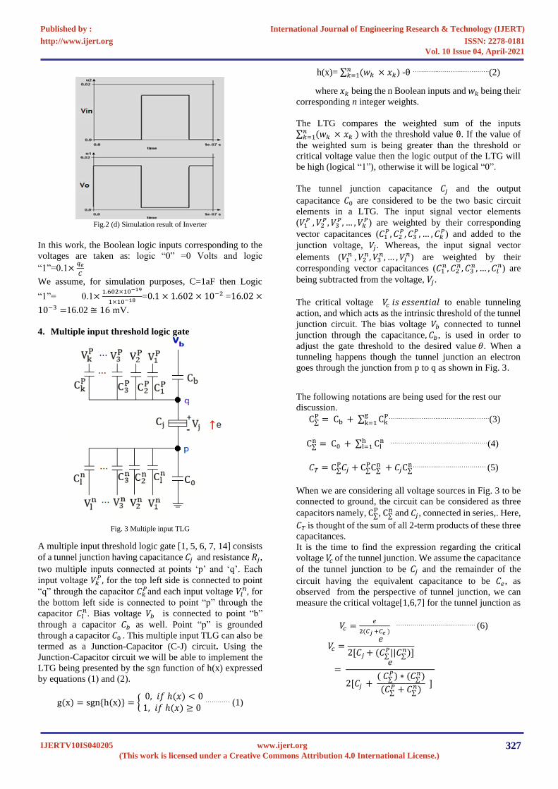
Fig.2 (d) Simulation result of Inverter
In this work, the Boolean logic inputs corresponding to the
voltages are taken as: logic “0” =0 Volts and logic
“1”=0.1×𝑞𝑒
𝐶
We assume, for simulation purposes, C=1aF then Logic
“1”= 0.1×1.602×10−19
1×10−18 =0.1 × 1.602 × 10−2 =16.02 ×
10−3 =16.02 ≅ 16 mV.
4. Multiple input threshold logic gate
Fig. 3 Multiple input TLG
A multiple input threshold logic gate [1, 5, 6, 7, 14] consists
of a tunnel junction having capacitance 𝐶𝑗 and resistance 𝑅𝑗,
two multiple inputs connected at points ‘p’ and ‘q’. Each
input voltage 𝑉𝑘𝑃 , for the top left side is connected to point
“q” through the capacitor 𝐶𝑘𝑃and each input voltage 𝑉𝑙
𝑛, for
the bottom left side is connected to point “p” through the
capacitor 𝐶𝑙𝑛. Bias voltage 𝑉𝑏 is connected to point “b”
through a capacitor 𝐶𝑏 as well. Point “p” is grounded
through a capacitor 𝐶0 . This multiple input TLG can also be
termed as a Junction-Capacitor (C-J) circuit. Using the
Junction-Capacitor circuit we will be able to implement the
LTG being presented by the sgn function of h(x) expressed
by equations (1) and (2).
g(x) = sgn{h(x)} = { 0, 𝑖𝑓 ℎ(𝑥) < 01, 𝑖𝑓 ℎ(𝑥) ≥ 0
………… (1)
h(x)= ∑ (𝑤𝑘 ×𝑛𝑘=1 𝑥𝑘) -θ ………….…………………….(2)
where 𝑥𝑘 being the n Boolean inputs and 𝑤𝑘 being their
corresponding n integer weights.
The LTG compares the weighted sum of the inputs ∑ (𝑤𝑘 ×𝑛
𝑘=1 𝑥𝑘 ) with the threshold value θ. If the value of
the weighted sum is being greater than the threshold or
critical voltage value then the logic output of the LTG will
be high (logical “1”), otherwise it will be logical “0”.
The tunnel junction capacitance 𝐶𝑗 and the output
capacitance 𝐶0 are considered to be the two basic circuit
elements in a LTG. The input signal vector elements
(𝑉1𝑃 , 𝑉2
𝑃 , 𝑉3𝑃, … , 𝑉𝑘
𝑃) are weighted by their corresponding
vector capacitances (𝐶1𝑃, 𝐶2
𝑃, 𝐶3𝑃, … , 𝐶𝑘
𝑃) and added to the
junction voltage, 𝑉𝑗. Whereas, the input signal vector
elements (𝑉1𝑛 , 𝑉2
𝑛, 𝑉3𝑛, … , 𝑉𝑙
𝑛) are weighted by their
corresponding vector capacitances (𝐶1𝑛, 𝐶2
𝑛, 𝐶3𝑛, … , 𝐶𝑙
𝑛) are
being subtracted from the voltage, 𝑉𝑗.
The critical voltage 𝑉𝑐 𝑖𝑠 𝑒𝑠𝑠𝑒𝑛𝑡𝑖𝑎𝑙 to enable tunneling
action, and which acts as the intrinsic threshold of the tunnel
junction circuit. The bias voltage 𝑉𝑏 connected to tunnel
junction through the capacitance, 𝐶𝑏, is used in order to
adjust the gate threshold to the desired value 𝜃. When a
tunneling happens though the tunnel junction an electron
goes through the junction from p to q as shown in Fig. 3.
The following notations are being used for the rest our
discussion.
C∑P = Cb + ∑ Ck
Pgk=1
……………………..……………………(3)
C∑n = C0 + ∑ Cl
n hl=1
…………………………………………(4)
𝐶𝑇 = C∑P𝐶𝑗 + C∑
PC∑n + 𝐶𝑗C∑
n……………………………… (5)
When we are considering all voltage sources in Fig. 3 to be
connected to ground, the circuit can be considered as three
capacitors namely, C∑P, C∑
n and 𝐶𝑗, connected in series,. Here,
𝐶𝑇 is thought of the sum of all 2-term products of these three
capacitances.
It is the time to find the expression regarding the critical
voltage 𝑉𝑐 of the tunnel junction. We assume the capacitance
of the tunnel junction to be 𝐶𝑗 and the remainder of the
circuit having the equivalent capacitance to be 𝐶𝑒, as
observed from the perspective of tunnel junction, we can
measure the critical voltage[1,6,7] for the tunnel junction as
𝑉𝑐 =𝑒
2(𝐶𝑗 +𝐶𝑒 ) ………………………………… (6)
𝑉𝑐 =𝑒
2[𝐶𝑗 + (𝐶∑𝑃||𝐶∑
𝑛)]
= 𝑒
2[𝐶𝑗 + ( 𝐶∑
𝑃) ∗ (𝐶∑𝑛)
(𝐶∑𝑃 + 𝐶∑
𝑛) ]
International Journal of Engineering Research & Technology (IJERT)
ISSN: 2278-0181http://www.ijert.org
IJERTV10IS040205(This work is licensed under a Creative Commons Attribution 4.0 International License.)
Published by :
www.ijert.org
Vol. 10 Issue 04, April-2021
327
= 𝑒(𝐶∑
𝑃 + 𝐶∑𝑛)
2[𝐶𝑗 ∗ (𝐶∑𝑃 + 𝐶∑
𝑛) + ( 𝐶∑𝑃) ∗ (𝐶∑
𝑛)]
= 𝑒(𝐶∑
𝑃+𝐶∑𝑛)
2𝐶𝑇 …………………………………….(7)
When the voltage across the junction is 𝑉𝑗 , a tunnel event
will happen through this tunnel junction if and only if the
condition given below is satisfied.
|𝑉𝑗| ≥ 𝑉𝑐……………………………………….(8)
If the junction voltage is less than the critical voltage i.e.
|𝑉𝑗| < 𝑉𝑐 , no tunneling events through the tunnel junction
happen. As a result, the tunneling circuit stays in a
𝑠𝑡𝑎𝑏𝑙𝑒 𝑠𝑡𝑎𝑡𝑒.
Theoretically, the thresholds are being integer numbers. And
the threshold logic equations for two input logic AND, OR,
NAND and NOR gates can be expressed [6] as follows.
𝐴𝑁𝐷(𝑃, 𝑄) = 𝑠𝑔𝑛{𝑃 + 𝑄 − 2}………… (9) 𝑂𝑅(𝑃, 𝑄) = 𝑠𝑔𝑛{𝑃 + 𝑄 − 1}……………(10) 𝑁𝐴𝑁𝐷(𝑃, 𝑄) = 𝑠𝑔𝑛{−𝑃 − 𝑄 + 2} …… (11) 𝑁𝑂𝑅(𝑃, 𝑄) = 𝑠𝑔𝑛{−𝑃 − 𝑄 + 1} ………(12)
If the threshold "θ" equals to "𝑖 "(i being an integer value),
this implies that the gates perform their functions correctly
for any value in the range [𝑖 −1 < θ ≤ 𝑖 ]. For the purpose
of maximizing robustness for variations in parameter values,
the threshold value θ = 𝑖 can be replaced by the
average θ = 𝑖 − 0.5. As a result, we will be able to express
the threshold logic equations for the two-input AND, OR,
NAND and NOR gates as below:
𝐴𝑁𝐷(𝑃, 𝑄) = 𝑠𝑔𝑛{𝑃 + 𝑄 − 1.5}……… (13) 𝑂𝑅(𝑃, 𝑄) = 𝑠𝑔𝑛{𝑃 + 𝑄 − 0.5}………… (14) 𝑁𝐴𝑁𝐷(𝑃, 𝑄) = 𝑠𝑔𝑛{−𝑃 − 𝑄 + 1.5} … (15) 𝑁𝑂𝑅(𝑃, 𝑄) = 𝑠𝑔𝑛{−𝑃 − 𝑄 + 0.5}……. (16)
The threshold gate-based implementations of the Boolean
Logic gates have the same basic circuit topology will be
drawn in the subsequent sections. The threshold gates
consist of a bias capacitance 𝐶𝑏, a tunnel junction
capacitance 𝐶𝑗 , and an output capacitance 𝐶0 and they are
connected in series. The AND and OR gates contain two
input capacitors C1 P 𝑎𝑛𝑑 C2
P . For both the 𝐴𝑁𝐷 and 𝑂𝑅
gates, the two input capacitances are C1 P = C2
P = 0.5𝐶 for
positively weighted inputs. On the contrary, for the NAND
and NOR gates, two capacitors bearing the values C1 n =
C2n = 0.5𝐶 for negatively weighted inputs.
Each threshold gates is augmented with an inverter/buffer
for stable output. The logic function done by the buffered
threshold gate is being the complement of “which is done by
the threshold gate itself”. For instance, a buffered 𝑁𝐴𝑁𝐷
gate implements the 𝐴𝑁𝐷 function. For the rest of our
discussion, when we are referring to a logic function such as
AND, we enforce that the logic function totally performed
by the entire gate (i.e., threshold gate plus an output buffer).
The parameters used for the constructing elements and
simulations of different gates like AND, OR, NAND and
NOR gates and other combinational or sequential circuits
are given in Table-1 [6,7].
Table-1 TLG 2-inout
AND
2-inout
OR
2-inout
NAND
2-inout
NOR
3-inout
OR
Cb 10.6C 11.7C 13.2C 11.7C 1 1.8C
C0 8C 8C 9C 9C 7.8C
C1P - - 0.5C 0.5C 0.4C
C2p - - 0.5C 0.5C -
C1n 0.5C 0.5C - - 0.5C
C2n 0.5C 0.5C - - -
𝐶𝑗 0.1C 0.1C 0.1C 0.1C 0.1C
Cg1
= Cg2
0.5C 0.5C 0.5C 0.5C 0.5C
C2
= C3
0.1C 0.1C 0.1C 0.1C 0.1C
C2
= C3
0.5C 0.5C 0.5C 0.5C 0.5C
C1
= C4
4.25C 4.25C 4.25C 4.25C 4.25C
CL 9C 9C 9C 9C 9C
𝑙𝑜𝑔𝑖𝑐 0 = 0 𝑉, 𝑙𝑜𝑔𝑖𝑐 1 = 16𝑚 𝑉, 𝑅𝑗= 105Ω, 𝐶𝑗=0.1aF, other
capacitance values are in terms of 𝐶, where 𝐶 = 1 𝑎𝐹
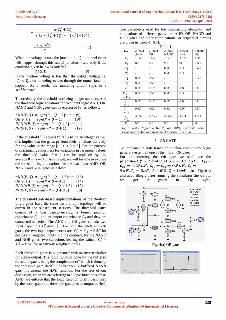
5. OR GATE
To implement a state transition pipeline circuit some logic
gates are essential, one of them is an OR gate.
For implementing the OR gate we shall use the
parameters𝐶1𝑛 = 𝐶2
𝑛=0.5aF,𝐶3 = 11.7𝑎𝐹, 𝑪𝒃𝟏 =𝑪𝒃𝟐 = 4.25𝑎𝐹, 𝐶𝑔1 = 𝐶𝑔2 = 0.5𝑎𝐹, 𝐶𝐿 =
9𝑎𝐹, 𝐶0 = 8𝑎𝐹, 𝑅𝑗=105Ω, 𝑉𝑠 = 16𝑚𝑉 in Fig.4(a)
and accordingly after running the simulator the output
we get is given in Fig. 4(b).
Fig. 4(a) OR gate
International Journal of Engineering Research & Technology (IJERT)
ISSN: 2278-0181http://www.ijert.org
IJERTV10IS040205(This work is licensed under a Creative Commons Attribution 4.0 International License.)
Published by :
www.ijert.org
Vol. 10 Issue 04, April-2021
328
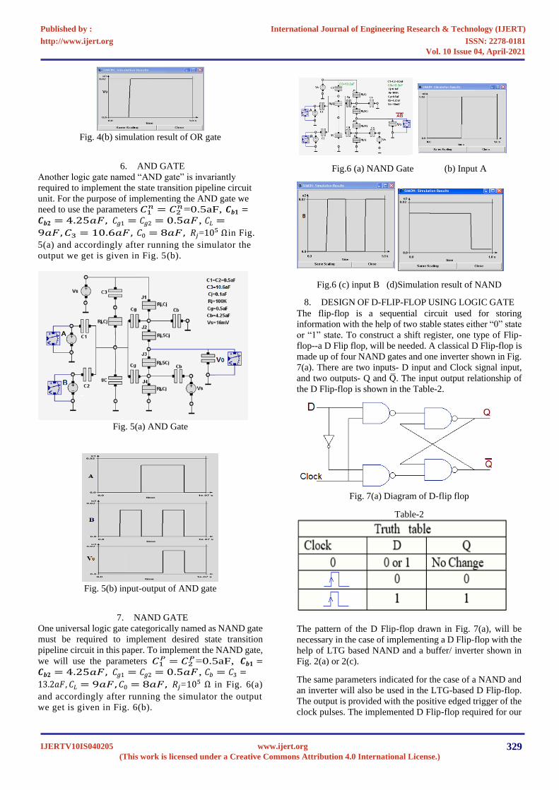
Fig. 4(b) simulation result of OR gate
6. AND GATE
Another logic gate named “AND gate” is invariantly
required to implement the state transition pipeline circuit
unit. For the purpose of implementing the AND gate we
need to use the parameters 𝐶1𝑛 = 𝐶2
𝑛=0.5aF, 𝑪𝒃𝟏 =𝑪𝒃𝟐 = 4.25𝑎𝐹, 𝐶𝑔1 = 𝐶𝑔2 = 0.5𝑎𝐹, 𝐶𝐿 =
9𝑎𝐹, 𝐶3 = 10.6𝑎𝐹, 𝐶0 = 8𝑎𝐹, 𝑅𝑗=105 Ω in Fig.
5(a) and accordingly after running the simulator the
output we get is given in Fig. 5(b).
Fig. 5(a) AND Gate
Fig. 5(b) input-output of AND gate
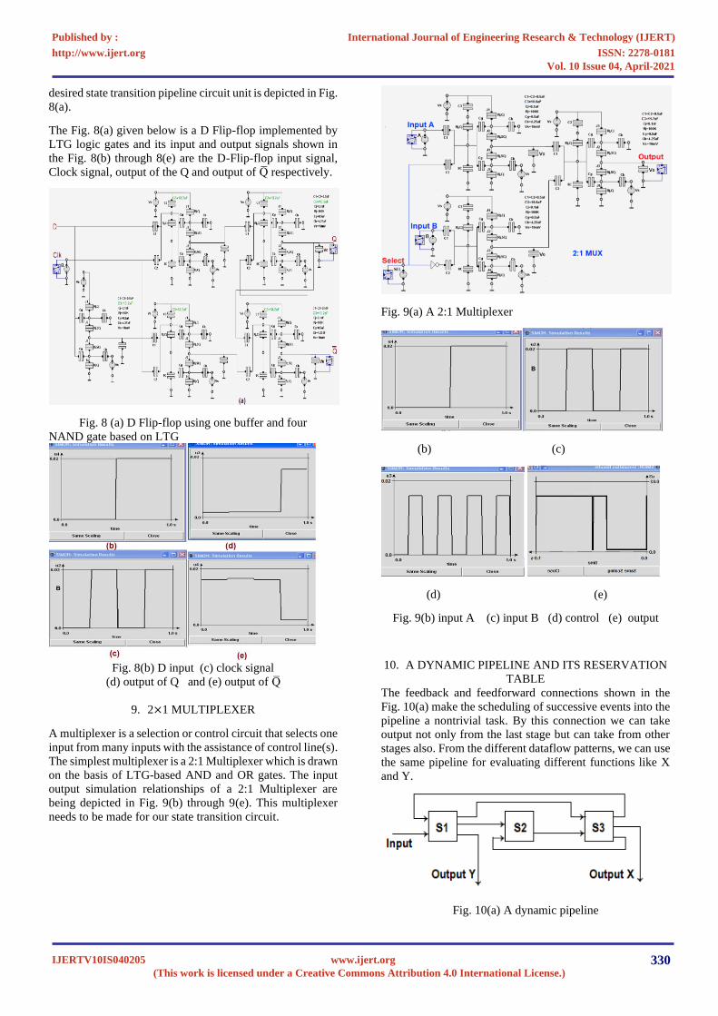
7. NAND GATE
One universal logic gate categorically named as NAND gate
must be required to implement desired state transition
pipeline circuit in this paper. To implement the NAND gate,
we will use the parameters 𝐶1𝑃 = 𝐶2
𝑃=0.5aF, 𝑪𝒃𝟏 =𝑪𝒃𝟐 = 4.25𝑎𝐹, 𝐶𝑔1 = 𝐶𝑔2 = 0.5𝑎𝐹, 𝐶𝑏 = 𝐶3 =
13.2𝑎𝐹, 𝐶𝐿 = 9𝑎𝐹, 𝐶0 = 8𝑎𝐹, 𝑅𝑗= 105 Ω in Fig. 6(a)
and accordingly after running the simulator the output
we get is given in Fig. 6(b).
Fig.6 (a) NAND Gate (b) Input A
Fig.6 (c) input B (d)Simulation result of NAND
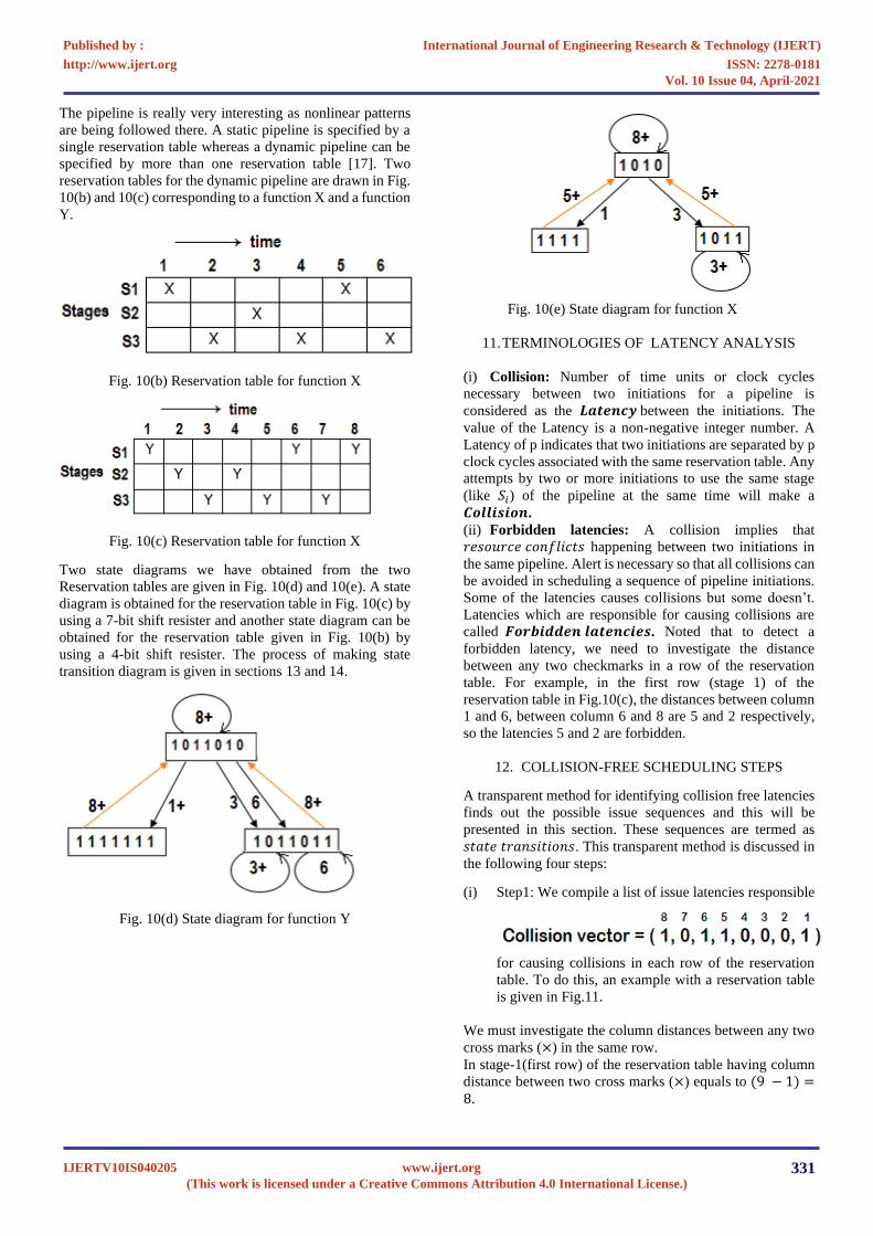
8. DESIGN OF D-FLIP-FLOP USING LOGIC GATE
The flip-flop is a sequential circuit used for storing
information with the help of two stable states either “0” state
or “1” state. To construct a shift register, one type of Flip-
flop--a D Flip flop, will be needed. A classical D Flip-flop is
made up of four NAND gates and one inverter shown in Fig.
7(a). There are two inputs- D input and Clock signal input,
and two outputs- Q and Q̅. The input output relationship of
the D Flip-flop is shown in the Table-2.
Fig. 7(a) Diagram of D-flip flop
Table-2
The pattern of the D Flip-flop drawn in Fig. 7(a), will be
necessary in the case of implementing a D Flip-flop with the
help of LTG based NAND and a buffer/ inverter shown in
Fig. 2(a) or 2(c).
The same parameters indicated for the case of a NAND and
an inverter will also be used in the LTG-based D Flip-flop.
The output is provided with the positive edged trigger of the
clock pulses. The implemented D Flip-flop required for our
International Journal of Engineering Research & Technology (IJERT)
ISSN: 2278-0181http://www.ijert.org
IJERTV10IS040205(This work is licensed under a Creative Commons Attribution 4.0 International License.)
Published by :
www.ijert.org
Vol. 10 Issue 04, April-2021
329
desired state transition pipeline circuit unit is depicted in Fig.
8(a).
The Fig. 8(a) given below is a D Flip-flop implemented by
LTG logic gates and its input and output signals shown in
the Fig. 8(b) through 8(e) are the D-Flip-flop input signal,
Clock signal, output of the Q and output of Q̅ respectively.
Fig. 8 (a) D Flip-flop using one buffer and four
NAND gate based on LTG
Fig. 8(b) D input (c) clock signal
(d) output of Q and (e) output of Q̅
9. 2×1 MULTIPLEXER
A multiplexer is a selection or control circuit that selects one
input from many inputs with the assistance of control line(s).
The simplest multiplexer is a 2:1 Multiplexer which is drawn
on the basis of LTG-based AND and OR gates. The input
output simulation relationships of a 2:1 Multiplexer are
being depicted in Fig. 9(b) through 9(e). This multiplexer
needs to be made for our state transition circuit.
Fig. 9(a) A 2:1 Multiplexer
(b) (c)
(d) (e)
Fig. 9(b) input A (c) input B (d) control (e) output
10. A DYNAMIC PIPELINE AND ITS RESERVATION
TABLE
The feedback and feedforward connections shown in the
Fig. 10(a) make the scheduling of successive events into the
pipeline a nontrivial task. By this connection we can take
output not only from the last stage but can take from other
stages also. From the different dataflow patterns, we can use
the same pipeline for evaluating different functions like X
and Y.
Fig. 10(a) A dynamic pipeline
International Journal of Engineering Research & Technology (IJERT)
ISSN: 2278-0181http://www.ijert.org
IJERTV10IS040205(This work is licensed under a Creative Commons Attribution 4.0 International License.)
Published by :
www.ijert.org
Vol. 10 Issue 04, April-2021
330
The pipeline is really very interesting as nonlinear patterns
are being followed there. A static pipeline is specified by a
single reservation table whereas a dynamic pipeline can be
specified by more than one reservation table [17]. Two
reservation tables for the dynamic pipeline are drawn in Fig.
10(b) and 10(c) corresponding to a function X and a function
Y.
Fig. 10(b) Reservation table for function X
Fig. 10(c) Reservation table for function X
Two state diagrams we have obtained from the two
Reservation tables are given in Fig. 10(d) and 10(e). A state
diagram is obtained for the reservation table in Fig. 10(c) by
using a 7-bit shift resister and another state diagram can be
obtained for the reservation table given in Fig. 10(b) by
using a 4-bit shift resister. The process of making state
transition diagram is given in sections 13 and 14.
Fig. 10(d) State diagram for function Y
Fig. 10(e) State diagram for function X
11. TERMINOLOGIES OF LATENCY ANALYSIS
(i) Collision: Number of time units or clock cycles
necessary between two initiations for a pipeline is
considered as the 𝑳𝒂𝒕𝒆𝒏𝒄𝒚 between the initiations. The
value of the Latency is a non-negative integer number. A
Latency of p indicates that two initiations are separated by p
clock cycles associated with the same reservation table. Any
attempts by two or more initiations to use the same stage
(like 𝑆𝑖) of the pipeline at the same time will make a
𝑪𝒐𝒍𝒍𝒊𝒔𝒊𝒐𝒏.
(ii) Forbidden latencies: A collision implies that
𝑟𝑒𝑠𝑜𝑢𝑟𝑐𝑒 𝑐𝑜𝑛𝑓𝑙𝑖𝑐𝑡𝑠 happening between two initiations in
the same pipeline. Alert is necessary so that all collisions can
be avoided in scheduling a sequence of pipeline initiations.
Some of the latencies causes collisions but some doesn’t.
Latencies which are responsible for causing collisions are
called 𝑭𝒐𝒓𝒃𝒊𝒅𝒅𝒆𝒏 𝒍𝒂𝒕𝒆𝒏𝒄𝒊𝒆𝒔. Noted that to detect a
forbidden latency, we need to investigate the distance
between any two checkmarks in a row of the reservation
table. For example, in the first row (stage 1) of the
reservation table in Fig.10(c), the distances between column
1 and 6, between column 6 and 8 are 5 and 2 respectively,
so the latencies 5 and 2 are forbidden.
12. COLLISION-FREE SCHEDULING STEPS
A transparent method for identifying collision free latencies
finds out the possible issue sequences and this will be
presented in this section. These sequences are termed as
𝑠𝑡𝑎𝑡𝑒 𝑡𝑟𝑎𝑛𝑠𝑖𝑡𝑖𝑜𝑛𝑠. This transparent method is discussed in
the following four steps:
(i) Step1: We compile a list of issue latencies responsible
for causing collisions in each row of the reservation
table. To do this, an example with a reservation table
is given in Fig.11.
We must investigate the column distances between any two
cross marks (×) in the same row.
In stage-1(first row) of the reservation table having column
distance between two cross marks (×) equals to (9 − 1) =8.
International Journal of Engineering Research & Technology (IJERT)
ISSN: 2278-0181http://www.ijert.org
IJERTV10IS040205(This work is licensed under a Creative Commons Attribution 4.0 International License.)
Published by :
www.ijert.org
Vol. 10 Issue 04, April-2021
331
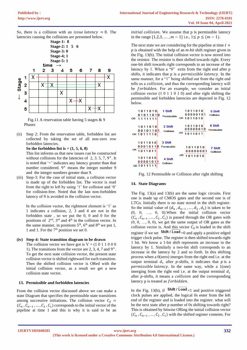
So, there is a collision with an 𝑖𝑠𝑠𝑢𝑒 𝑙𝑎𝑡𝑒𝑛𝑐𝑦 = 8. The
latencies causing the collisions are presented below.
Stage-1: 8
Stage-2: 1 5 6
Stage-3: 0
Stage-4; 1
Stage-5: 1
Fig.11 A reservation table having 5 stages & 9
Phases
(ii) Step 2: From the reservation table, forbidden list are
collected by taking the set of all non-zero row
forbidden latencies.
So the forbidden list is = (1, 5, 6, 8)
This list informs us that new issues can be constructed
without collisions for the latencies of 2, 3. 5, 7, 9+. It
is noted that ‘+’ indicates any latency greater than that
number considered. 9+ means the integer number 9
and the integer numbers greater than 9.
(iii) Step-3: For the case of initial state, a collision vector
is made up of the forbidden list. The vector is read
from the right to left by using ‘1’ for collision and ‘0’
for collision-free. Noted that the last non-forbidden
latency of 9 is avoided in the collision vector.
In the collision vector, the rightmost element is ‘1’ as
1 indicates a collision, 2, 3 and 4 are not in the
forbidden state , so we put the 0, 0 and 0 for the
positions of 2nd, 3rd and 4th in the collision vector. In
the same manner, in positions 5th, 6th and 8th we put 1,
1 and 1. For the 7th position we set 0.
(iv) Step-4: State transition diagram to be drawn
The collision vector we have got is V = (1 0 1 1 0 0 0
1). The transitions from the vector are 2, 3, 4, 7 and 9+.
To get the next state collision vector, the present state
collision vector is shifted rightward for each transition.
Then the shifted collision vector is ORed with the
initial collision vector, as a result we get a new
collision state vector.
13. Permissible and forbidden latencies
From the collision vector discussed above we can make a
state Diagram that specifies the permissible state transitions
among successive initiations. The collision vector 𝐶𝑋 =(𝐶𝑛 , 𝐶𝑛−1 , … , 𝐶2 , 𝐶1) corresponds to the initial vector of the
pipeline at time 1 and this is why it is said to be an
𝑖𝑛𝑖𝑡𝑖𝑎𝑙 𝑐𝑜𝑙𝑙𝑖𝑠𝑖𝑜𝑛. We assume that p is permissible latency
in the range {1,2,3, … . , 𝑚 − 1} i.e., 1≤ 𝑝 ≤ (𝑚 − 1).
The next state we are considering for the pipeline at time 𝑡 +𝑝 is obtained with the help of an m-bit shift register given in
the Fig. 13(b). The initial collision vector is now stored into
the resistor. The resistor is then shifted towards right. Every
one-bit shift towards right corresponds to an increase of the
latency by 1. When a “0” exits from the right end after p
shifts, it indicates that p is a 𝑝𝑒𝑟𝑚𝑖𝑠𝑠𝑖𝑏𝑙𝑒 𝑙𝑎𝑡𝑒𝑛𝑐𝑦. In the
same manner, for a “1” being shifted out from the right end
tells us a 𝑐𝑜𝑙𝑙𝑖𝑠𝑖𝑜𝑛, and thus the corresponding latency will
be 𝑓𝑜𝑟𝑏𝑖𝑑𝑑𝑒𝑛. For an example, we consider an initial
collision vector (1 0 1 1 0 1 0) and after right shifting the
permissible and forbidden latencies are depicted in Fig. 12
below.
Fig. 12 Permissible or Collision after right shifting
14. State Diagrams
The Fig. 13(a) and 13(b) are the same logic circuits. First
one is made up of CMOS gates and the second one is of
LTGs. Initially there is no state stored in the shift register.
So the initial value of (𝑑𝑛 , 𝑑𝑛−1 , … , 𝑑2 , 𝑑1) is taken to be
(0, 0, …, 0, 0).When the initial collision vector
(𝐶𝑛 , 𝐶𝑛−1 , … , 𝐶2 , 𝐶1) is passed through the OR gates with
(0, 0, …, 0, 0), we get the same output of OR gates as the
collision vector is. And this vector 𝐶𝑋 is loaded in the shift
register if we set =0 and apply a positive edged
trigger clock pulse. The register is then shifted towards right
1 bit. We know a 1-bit shift represents an increase in the
latency by 1. Similarly a two-bit shift corresponds to an
increase in the latency by 2 and so forth. In this shifting
process when a 0(zero) imerges from the right end i.e. at the
output terminal 𝑑1 after 𝑝-shifts, it indicates that 𝑝 is a
𝑝𝑒𝑟𝑚𝑖𝑠𝑠𝑖𝑏𝑙𝑒 𝑙𝑎𝑡𝑒𝑛𝑐𝑦. In the same way, while a 1(one)
imerging from the right end i.e. at the output terminal 𝑑1
after 𝑝-shifts, it means a 𝑐𝑜𝑙𝑙𝑖𝑠𝑖𝑜𝑛 and the corresponding
latency p is treated as 𝑓𝑜𝑟𝑏𝑖𝑑𝑑𝑒𝑛.
In the Fig. 13(b), if =1 and positive triggered
clock pulses are applied, the logical 0s enter from the left
end of the register and is loaded into the register. what will
be the next state after p number of 0s shifting towards right?
This is obtained by bitwise ORing the initial collision vector
(𝐶𝑛 , 𝐶𝑛−1 , … , 𝐶2 , 𝐶1) with the shifted register contents. For
International Journal of Engineering Research & Technology (IJERT)
ISSN: 2278-0181http://www.ijert.org
IJERTV10IS040205(This work is licensed under a Creative Commons Attribution 4.0 International License.)
Published by :
www.ijert.org
Vol. 10 Issue 04, April-2021
332
instance, the initial collision vector we assumed to be = (1 0
1 1 0 1 0) and which will really be the shift register’s
contents. After 1 right shift the contents of the shift register
will be = (0 1 0 1 1 0 1). These two vectors are bit-wise ORed
and we have the next state (1 1 1 1 1 1 1 ). After 2 shift, 4
shift, 5 shift, 7 shift there will be collision states.
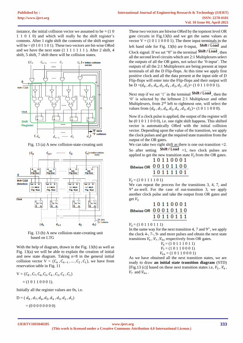
Fig. 13 (a) A new collision-state-creating unit
Fig. 13 (b) A new collision-state-creating unit
based on LTG
With the help of diagram, drawn in the Fig. 13(b) as well as
Fig. 13(a) we will be able to explain the creation of initial
and new state diagram. Taking n=8 in the general initial
collision vector V = (𝐶𝑛 , 𝐶𝑛−1 , … , 𝐶2 , 𝐶1), we have from
reservation table in Fig. 11
V = (𝐶8 , 𝐶7, 𝐶6, 𝐶5, 𝐶4 , 𝐶3, 𝐶2 , 𝐶1)
= (1 0 1 1 0 0 0 1).
Initially all the register values are 0s, i.e.
D = ( 𝑑8 , 𝑑7, 𝑑6, 𝑑5, 𝑑4 , 𝑑3, 𝑑2 , 𝑑1)
= (0 0 0 0 0 0 0 0)
These two vectors are bitwise ORed by the topmost level OR
gate circuits in Fig.13(b) and we get the same values as
vector V = (1 0 1 1 0 0 0 1). The three input terminals in the
left hand side for Fig. 13(b) are 0-input, and
Clock signal. If we set “0” in the terminal , then
all the second level circuits which are 2:1 Multiplexers select
the outputs of all the OR gates, not select the ‘0-input’. The
outputs of all the 2:1 Multiplexers are being present at input
terminals of all the D Flip-flops. At this time we apply first
positive clock and all the data present at the input side of D
Flip-flops will enter into the Flip-flops and their output will
be D =(𝑑8 , 𝑑7, 𝑑6, 𝑑5, 𝑑4 , 𝑑3, 𝑑2 , 𝑑1)= (1 0 1 1 0 0 0 1).
Next step if we set ‘1’ in the terminal , then the
‘0’ is selected by the leftmost 2:1 Multiplexer and other
Multiplexers, from 2nd left to rightmost one, will select the
values from (𝑑8 , 𝑑7, 𝑑6, 𝑑5, 𝑑4 , 𝑑3, 𝑑2)= (1 0 1 1 0 0 0).
Now if a clock pulse is applied, the output of the register will
be (0 1 0 1 1 0 0 0), i.e. one right shift happens. This shifted
vector is automatically ORed with the initial collision
vector. Depending upon the value of the transition, we apply
the clock pulses and get the required state transition from the
output of the OR gates.
We can take two right shift as there is one out-transition =2.
So after setting =1, two clock pulses are
applied to get the new transition state 𝑉2 from the OR gates.
𝑉2 = (1 0 1 1 1 1 0 1)
We can repeat the process for the transitions 3, 4, 7, and
9+ 𝑎𝑠 𝑤𝑒𝑙𝑙. For the case of out-transition 3, we apply
another clock pulse and take the output from OR gates and
get 𝑉3
𝑉3 = (1 0 1 1 0 1 1 1)
In the same way for the next transition 4, 7 and 9+, we apply
the clock 4-, 7-, 9- and more pulses and obtain the next state
transitions 𝑉4 , 𝑉7 , 𝑉9+ respectively from OR gates.
𝑉4 = (1 0 1 1 1 0 1 1)
𝑉7 = (1 0 1 1 0 0 0 1)
𝑉9+ = (1 0 1 1 0 0 0 1)
As we have obtained all the next transition states, we are
ready to draw an initial state transition diagram (STD)
[Fig.13 (c)] based on these next transition states i.e, 𝑉3 , 𝑉4 ,
𝑉7 and 𝑉9+ .
International Journal of Engineering Research & Technology (IJERT)
ISSN: 2278-0181http://www.ijert.org
IJERTV10IS040205(This work is licensed under a Creative Commons Attribution 4.0 International License.)
Published by :
www.ijert.org
Vol. 10 Issue 04, April-2021
333
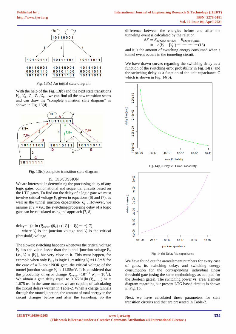
Fig. 13(c) An initial state diagram
With the help of the Fig. 13(b) and the next state transitions
𝑉2 , 𝑉3 , 𝑉4 , 𝑉7 , 𝑉9+ , we can find all the new transition states
and can draw the “complete transition state diagram” as
shown in Fig. 13(d).
Fig. 13(d) complete transition state diagram
15. DISCUSSION
We are interested in determining the processing delay of any
logic gates, combinational and sequential circuits based on
the LTG gates. To find out the delay of a logic gate we must
involve critical voltage 𝑉𝑐 given in equations (6) and (7), as
well as the tunnel junction capacitance 𝐶𝑗 . However, we
assume at T = 0K, the switching/processing delay of a logic
gate can be calculated using the approach [7, 8].
delay=−(𝑒|ln (𝑃𝑒𝑟𝑟𝑜𝑟 )|𝑅𝑡) / ( |𝑉𝑗| − 𝑉𝑐) ……..(17)
where 𝑉𝑗 is the junction voltage and 𝑉𝑐 is the critical
(threshold) voltage
The slowest switching happens whenever the critical voltage
𝑉𝑐 has the value lesser than the tunnel junction voltage 𝑉𝑗,
i.e., 𝑉𝑐 < |𝑉𝑗 |, but very close to it. This must happen, for
example when only 𝑉𝑖𝑛1 is logic 1, resulting 𝑉𝑗 =11.8mV for
the case of a 2-input NOR gate, the critical voltage of the
tunnel junction voltage 𝑉𝑐 is 11.58mV. It is considered that
the probability of error change 𝑃𝑒𝑟𝑟𝑜𝑟 =10−12, 𝑅𝑡 = 105Ω.
We obtain a gate delay equal to 0.07281|ln (𝑃𝑒𝑟𝑟𝑜𝑟 )|ns =
1.675 ns. In the same manner, we are capable of calculating
the circuit delays written in Table-2. When a charge tunnels
through the tunnel junction, the amount of total energy in the
circuit changes before and after the tunneling. So the
difference between the energies before and after the
tunneling event is calculated by the relation
Δ𝐸 = 𝐸𝑏𝑒𝑓𝑜𝑟𝑒 𝑡𝑢𝑛𝑛𝑒𝑙 − 𝐸𝑎𝑓𝑡𝑒𝑟 𝑡𝑢𝑛𝑛𝑒𝑙
= −𝑒(𝑉𝑐 − |𝑉𝑗|)……………………..(18)
and it is the amount of switching energy consumed when a
tunnel event occurs in the tunneling circuit.
We have drawn curves regarding the switching delay as a
function of the switching error probability in Fig. 14(a) and
the switching delay as a function of the unit capacitance C
which is shown in Fig. 14(b).
Fig. 14(a) Delay vs. Error Probability
Fig. 14 (b) Delay Vs. capacitance
We have found out the area/element numbers for every case
of gates, its switching delay, and switching energy
consumption for the corresponding individual linear
threshold gate (using the same methodology as adopted for
the Boolean gates). The switching power vs. area/ element
diagram regarding our present LTG based circuits is shown
in Fig. 15.
Next, we have calculated those parameters for state
transition circuits and that are presented in Table-2.
International Journal of Engineering Research & Technology (IJERT)
ISSN: 2278-0181http://www.ijert.org
IJERTV10IS040205(This work is licensed under a Creative Commons Attribution 4.0 International License.)
Published by :
www.ijert.org
Vol. 10 Issue 04, April-2021
334
In the Fig.13(b), time delays for the phase-1 is
0.340|ln(𝑃𝑒𝑟𝑟𝑜𝑟)|ns, for phase-2 is 0.5|ln(𝑃𝑒𝑟𝑟𝑜𝑟)| ns, for
phase-3 is 0.66|ln(𝑃𝑒𝑟𝑟𝑜𝑟)| ns, for phase-4 is .82|ln(𝑃𝑒𝑟𝑟𝑜𝑟)|
ns, … and for phase-n is (0.340+0.160× (𝑛 −1))|ln(𝑃𝑒𝑟𝑟𝑜𝑟)|ns. With the assistance of the data taken from
table-2, the processing/ switching delay of a State transition
diagram of a pipeline unit having phases n is (0.340+0.160×(𝑛 − 1))|ln(𝑃𝑒𝑟𝑟𝑜𝑟)|ns. We have discussed about collision
vector above having number of vector elements equal to 8.
Given that the value of 𝑃𝑒𝑟𝑟𝑜𝑟 equals to 10−10, so the time
after which the 8th bit of the register content will emerge
from the pipeline unit is
(0.340+0.160× (8 − 1))|ln(𝑃𝑒𝑟𝑟𝑜𝑟)| ns=26.13ns.
We are to determine the clock pulse duration and it is
determined by the maximum delay of an OR gate or a 2:1
Multiplexer or a D Flip-flop. From the Table-2 we are able
to get their delays and the maximum delay of them is ( 𝜏𝑚𝑎𝑥)
is given by
𝜏𝑚𝑎𝑥 = max{ 0.102|ln( 𝑃𝑒𝑟𝑟𝑜𝑟)|, 0.124|ln(𝑃𝑒𝑟𝑟𝑜𝑟)|,
0.160|ln( 𝑃𝑒𝑟𝑟𝑜𝑟)|}
=8.887ns ………………………………….(19)
Table-2
Fig. 15. Switching power vs. area/ element
Therefore the clock cycle time should be at least 8.887ns.
So the last 8th bit output will emerge after 26.13ns. If we
consider the Fib. 13(b) as a pipeline system,
then after every clock pulse of time 8.887ns one output will
emerge from terminal 𝑑1 in Fig. 13(b). If the value of n is a
big number then output rate or frequency of the pipeline will
be
𝑓 ≈1
26.13ns
= 38.27MHz…………………………… (20)
16. SWITCHING DELAYS OF LTG AND SET
The time delay/processing delay for a CMOS logic gate like
NAND, NOR, XOR is 12ns [20], whereas the time required
for tunneling through a single electron transistor (SET) is
approximately 4ns [4, 5, 16, 18]. The XOR gate using
conventional logic circuits requires 16 transistors, whereas
the same function can be implemented with the help of just
one SET [3, 5, 6, 11] i.e. number of nodes can be reduced to
1 in lieu of 16. Given that error probability is 10−15 then the
delay for the inverter will be 2.3025ns and similarly the
other delays for the other gates can be calculated and are
shown in Table-3. It is clear that the LTG based circuit is
faster than the SET based circuit when 𝑃𝑒𝑟𝑟𝑜𝑟=10−15. The
comparison of delays for SET and LTG gate based circuits
is drawn by a bar diagram in Fig.16.
International Journal of Engineering Research & Technology (IJERT)
ISSN: 2278-0181http://www.ijert.org
IJERTV10IS040205(This work is licensed under a Creative Commons Attribution 4.0 International License.)
Published by :
www.ijert.org
Vol. 10 Issue 04, April-2021
335
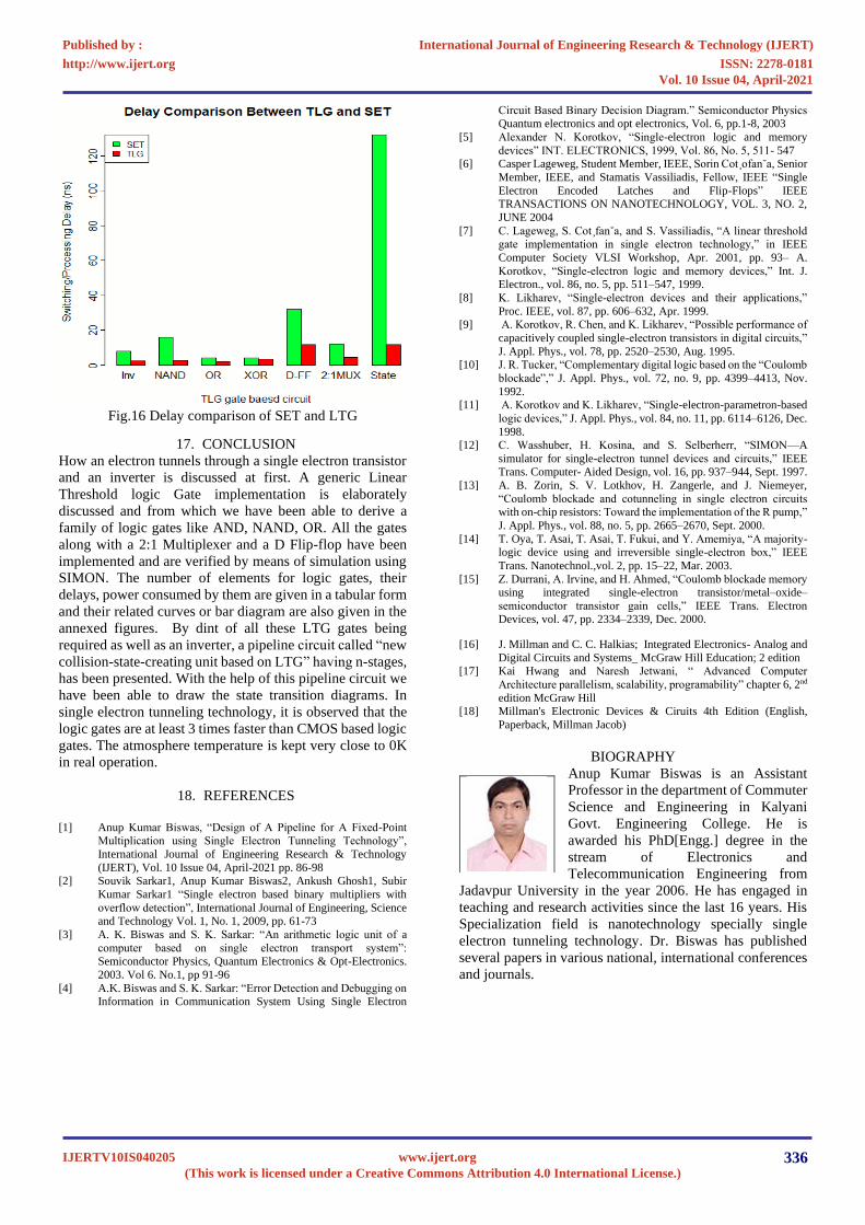
Fig.16 Delay comparison of SET and LTG
17. CONCLUSION
How an electron tunnels through a single electron transistor
and an inverter is discussed at first. A generic Linear
Threshold logic Gate implementation is elaborately
discussed and from which we have been able to derive a
family of logic gates like AND, NAND, OR. All the gates
along with a 2:1 Multiplexer and a D Flip-flop have been
implemented and are verified by means of simulation using
SIMON. The number of elements for logic gates, their
delays, power consumed by them are given in a tabular form
and their related curves or bar diagram are also given in the
annexed figures. By dint of all these LTG gates being
required as well as an inverter, a pipeline circuit called “new
collision-state-creating unit based on LTG” having n-stages,
has been presented. With the help of this pipeline circuit we
have been able to draw the state transition diagrams. In
single electron tunneling technology, it is observed that the
logic gates are at least 3 times faster than CMOS based logic
gates. The atmosphere temperature is kept very close to 0K
in real operation.
18. REFERENCES
[1] Anup Kumar Biswas, “Design of A Pipeline for A Fixed-Point
Multiplication using Single Electron Tunneling Technology”,
International Journal of Engineering Research & Technology
(IJERT), Vol. 10 Issue 04, April-2021 pp. 86-98 [2] Souvik Sarkar1, Anup Kumar Biswas2, Ankush Ghosh1, Subir
Kumar Sarkar1 “Single electron based binary multipliers with
overflow detection”, International Journal of Engineering, Science and Technology Vol. 1, No. 1, 2009, pp. 61-73
[3] A. K. Biswas and S. K. Sarkar: “An arithmetic logic unit of a
computer based on single electron transport system”:
Semiconductor Physics, Quantum Electronics & Opt-Electronics.
2003. Vol 6. No.1, pp 91-96
[4] A.K. Biswas and S. K. Sarkar: “Error Detection and Debugging on Information in Communication System Using Single Electron
Circuit Based Binary Decision Diagram.” Semiconductor Physics Quantum electronics and opt electronics, Vol. 6, pp.1-8, 2003
[5] Alexander N. Korotkov, “Single-electron logic and memory
devices” INT. ELECTRONICS, 1999, Vol. 86, No. 5, 511- 547 [6] Casper Lageweg, Student Member, IEEE, Sorin Cot¸ofan˘a, Senior
Member, IEEE, and Stamatis Vassiliadis, Fellow, IEEE “Single
Electron Encoded Latches and Flip-Flops” IEEE TRANSACTIONS ON NANOTECHNOLOGY, VOL. 3, NO. 2,
JUNE 2004
[7] C. Lageweg, S. Cot¸fan˘a, and S. Vassiliadis, “A linear threshold gate implementation in single electron technology,” in IEEE
Computer Society VLSI Workshop, Apr. 2001, pp. 93– A.
Korotkov, “Single-electron logic and memory devices,” Int. J. Electron., vol. 86, no. 5, pp. 511–547, 1999.
[8] K. Likharev, “Single-electron devices and their applications,”
Proc. IEEE, vol. 87, pp. 606–632, Apr. 1999. [9] A. Korotkov, R. Chen, and K. Likharev, “Possible performance of
capacitively coupled single-electron transistors in digital circuits,”
J. Appl. Phys., vol. 78, pp. 2520–2530, Aug. 1995. [10] J. R. Tucker, “Complementary digital logic based on the “Coulomb
blockade”,” J. Appl. Phys., vol. 72, no. 9, pp. 4399–4413, Nov.
1992. [11] A. Korotkov and K. Likharev, “Single-electron-parametron-based
logic devices,” J. Appl. Phys., vol. 84, no. 11, pp. 6114–6126, Dec.
1998. [12] C. Wasshuber, H. Kosina, and S. Selberherr, “SIMON—A
simulator for single-electron tunnel devices and circuits,” IEEE Trans. Computer- Aided Design, vol. 16, pp. 937–944, Sept. 1997.
[13] A. B. Zorin, S. V. Lotkhov, H. Zangerle, and J. Niemeyer,
“Coulomb blockade and cotunneling in single electron circuits with on-chip resistors: Toward the implementation of the R pump,”
J. Appl. Phys., vol. 88, no. 5, pp. 2665–2670, Sept. 2000.
[14] T. Oya, T. Asai, T. Asai, T. Fukui, and Y. Amemiya, “A majority-logic device using and irreversible single-electron box,” IEEE
Trans. Nanotechnol.,vol. 2, pp. 15–22, Mar. 2003.
[15] Z. Durrani, A. Irvine, and H. Ahmed, “Coulomb blockade memory using integrated single-electron transistor/metal–oxide–
semiconductor transistor gain cells,” IEEE Trans. Electron Devices, vol. 47, pp. 2334–2339, Dec. 2000.
[16] J. Millman and C. C. Halkias; Integrated Electronics- Analog and
Digital Circuits and Systems_ McGraw Hill Education; 2 edition [17] Kai Hwang and Naresh Jetwani, “ Advanced Computer
Architecture parallelism, scalability, programability” chapter 6, 2nd
edition McGraw Hill [18] Millman's Electronic Devices & Ciruits 4th Edition (English,
Paperback, Millman Jacob)
BIOGRAPHY
Anup Kumar Biswas is an Assistant
Professor in the department of Commuter
Science and Engineering in Kalyani
Govt. Engineering College. He is
awarded his PhD[Engg.] degree in the
stream of Electronics and
Telecommunication Engineering from
Jadavpur University in the year 2006. He has engaged in
teaching and research activities since the last 16 years. His
Specialization field is nanotechnology specially single
electron tunneling technology. Dr. Biswas has published
several papers in various national, international conferences
and journals.
International Journal of Engineering Research & Technology (IJERT)
ISSN: 2278-0181http://www.ijert.org
IJERTV10IS040205(This work is licensed under a Creative Commons Attribution 4.0 International License.)
Published by :
www.ijert.org
Vol. 10 Issue 04, April-2021
336
Related Documents