In this section we cover the following: • State graphs introduction • Serial Adder • Multiplier • Divider STATE GRAPHS FOR CONTROL NETWORKS What are the conditions for having a proper state graph? • If an arc is named XiXj/ZpZq then • if given inputs (XiXj) are 1( & other inputs would be don’t care), • then the specified outputs (ZpZq) are 1 (& the other outputs are zero). • If we have 4 inputs X1,X2,X3,X4 and 4 outputs Z1,Z2,Z3,Z4 then the label X1X4’/Z1Z3 is equivalent to 1- - 0/1010. (- is don’t care) • If we label an arc I, then the arc is traversed when I =1. • To have a completely specified proper state graph in which the next state is uniquely defined for every input combination the following conditions must be satisfied: 1. If Xi and Xj are any pair of input labels on arcs exiting state Sk, then XiXj=0 if i # j. This condition ensures that at most one condition is satisfied at any given point of time. 2. If n arcs exit state Sk and the n arcs have input labels X1,X2,….Xn then X1+X2+…..Xn =1. This ensures that at least one condition is satisfied. www.allsyllabus.com www.allsyllabus.com vtu.allsyllabus.com

Welcome message from author
This document is posted to help you gain knowledge. Please leave a comment to let me know what you think about it! Share it to your friends and learn new things together.
Transcript

In this section we cover the following:
• State graphs introduction
• Serial Adder
• Multiplier
• Divider
STATE GRAPHS FOR CONTROL NETWORKS
What are the conditions for having a proper state graph?
• If an arc is named XiXj/ZpZq then
• if given inputs (XiXj) are 1( & other inputs would be don’t care),
• then the specified outputs (ZpZq) are 1 (& the other outputs are zero).
• If we have 4 inputs X1,X2,X3,X4 and 4 outputs Z1,Z2,Z3,Z4 then the label
X1X4’/Z1Z3 is equivalent to 1- - 0/1010. (- is don’t care)
• If we label an arc I, then the arc is traversed when I =1.
• To have a completely specified proper state graph in which the next state is uniquely
defined for every input combination the following conditions must be satisfied:
1. If Xi and Xj are any pair of input labels on arcs exiting state Sk, then
XiXj=0 if i # j.
This condition ensures that at most one condition is satisfied at any given
point of time.
2. If n arcs exit state Sk and the n arcs have input labels X1,X2,….Xn then
X1+X2+…..Xn =1. This ensures that at least one condition is satisfied.
www.alls
yllab
us.co
m
www.allsyllabus.com
vtu.allsyllabus.com

A few examples illustrating the nomenclature in state graphs is presented in figures below.
Fig. Partial state graph showing that conditions 1 &2 are satisfied for state Sk.
Fig. a
Fig. Partial State Graph (Fig. a above) and its state table row for Sk.
www.alls
yllab
us.co
m
www.allsyllabus.com
vtu.allsyllabus.com

Serial adder with Accumulator
Question: Illustrate the design of a control circuit for a serial adder with Accumulator
Definition: A Control circuit in a digital system is a sequential network that outputs a
sequence of control signals.
These Control signals cause operations such as addition and shifting to take place at
appropriate times.
Block Diagram of a 4-bit Serial Adder with Accumulator
The Operation of Serial Adder whose block diagram is given above is illustrated with the
help of a table shown below.
www.alls
yllab
us.co
m
www.allsyllabus.com
vtu.allsyllabus.com

State Graph for Control Circuit of the Serial Adder
www.alls
yllab
us.co
m
www.allsyllabus.com
vtu.allsyllabus.com

Question: Draw the block diagram for a 16 bit serial adder with accumulator.
• The control network uses a 4 bit counter which outputs k=1 when it is in state 1111.
• When a start signal N is received, the registers should be loaded. Assume that N will
remain 1 until the addition is complete.
• When the addition is complete, the control network should go to a stop and remain there
until N is changed to 0.
• Draw a state diagram for the control network (excluding counter). Write the VHDL
code.
Fig. state diagram for the control network
www.alls
yllab
us.co
m
www.allsyllabus.com
vtu.allsyllabus.com

Fig. Block diagram for a 16 bit serial adder with accumulator
VHDL CODE for the 16 bit serial adder
library IEEE;
use IEEE.STD_LOGIC_1164.ALL;
use IEEE.STD_LOGIC_ARITH.ALL;
use IEEE.STD_LOGIC_UNSIGNED.ALL;
--library UNISIM;
--use UNISIM.VComponents.all;
Entity seradder is
Port (N,clk: in STD_LOGIC;
A: in STD_LOGIC_vector(15 downto 0);
R: out STD_LOGIC_vector(15 downto 0);
B: in STD_LOGIC_vector(15 downto 0);
Co:out STD_LOGIC);
End seradder;
Architecture mealy of seradder is
Signal si,ci,cip,ld,sh: STD_LOGIC:='0';
Signal k:STD_LOGIC:='0';
Signal acc,regb: STD_LOGIC_vector(15 downto 0);
Signal state: integer range 0 to 2:=0;
Signal nxst: integer range 0 to 2:=0;
Signal cnt: STD_LOGIC_vector(4 downto
0):="00000";
Begin
K<='1' when (cnt="10000") else '0';
Process(clk)
Begin
www.alls
yllab
us.co
m
www.allsyllabus.com
vtu.allsyllabus.com

If (clk='1' and clk' event) then
Case state is
when 0=> if (N='1') then ld<='1';sh<='1';acc<=A;
regb<=B;ci<='0'; state <=state+1;
Else state<=0; end if;
when 1 => if(k='1') then sh<='1'; state<=
state+1;R<= acc; Co<=cip;
else sh<='1';
acc<=si & acc(15 downto 1);
regb<= regb(0) & regb(15 downto 1);
Ci<=cip; cnt<=cnt+1; end if;
when 2=> if(N='0') then state <=0;
Else nxst<=state; end if;
End case;
End if; End process;
Si<= acc(0) xor regb(0) xor ci;
Cip<=( acc(0) and regb(0)) or (acc(0) and ci) or
(regb(0) and ci);
End mealy;
www.alls
yllab
us.co
m
www.allsyllabus.com
vtu.allsyllabus.com

Binary Multiplier
Multiplication of Two 4 bit numbers requires the following architecture
• 4-bit multiplicand register
• 4-bit multiplier register
• 4-bit full adder
• 8-bit product register which serves as an accumulator to accumulate the sum of partial
products.
Note: In the conventional adder Shifting multiplicand left every time would require an 8-bit
Adder. Instead we shift the contents of the product register right each time
The operation of the 4-bit binary multiplier shown in figure is elaborated in the below steps.
• 4-bits from accumulator and 4-bits from multiplicand register are inputs to adder.
• 4 sum bits and carry are connected back to accumulator.
• When an Ad signal occurs, adder outputs are transferred to ACC at next clk.
• Extra bit carries temporarily any carry that is generated.
• Sh signal causes all 9 bits to be shifted right at next clk.
• Multiplier is stored in lower 4 bits of ACC.
• Control circuit outputs proper sequence of add and shift signals after the start signal St=1.
www.alls
yllab
us.co
m
www.allsyllabus.com
vtu.allsyllabus.com

.
Fig. Block Diagram of Binary Multiplier
Multiplication Steps
www.alls
yllab
us.co
m
www.allsyllabus.com
vtu.allsyllabus.com

Algorithm:
1. If current multiplier bit M (LSB of acc) is 1, multiplicand is added to accumulator and
shifted right.
2. If M=0, addition is skipped and contents shifted right.
The below figure briefly illustrates the contents of the binary multiplier for the example
illustrated above.
www.alls
yllab
us.co
m
www.allsyllabus.com
vtu.allsyllabus.com

Question: What should the control circuit of the multiplier do??
• Output proper sequence of Ad and Sh signals.
• Start when S=1.
• Load; Ld=1.
• Check if M=1. If yes then make Ad=1 (to add). Then make Sh=1.
• If M =0, then don’t change Ad to 1. Just make Sh=1.
• A shift is always generated after Add operation.
• A done signal generated after 4 shifts (indicating multiplication is complete).
State Graph for Binary Multiplier Control
www.alls
yllab
us.co
m
www.allsyllabus.com
vtu.allsyllabus.com

VHDL code for 4 X 4 Binary Multiplier
The below code is a behavioral model of a multiplier for unsigned binary numbers. It multiplies
a 4-bit multiplicand by a 4-bit multiplier to give an 8-bit product. The maximum number of
clock cycles needed for a multiply is 10.
library BITLIB;
use BITLIB.bit_pack.all;
entity mult4X4 is
port (Clk, St: in bit;
Mplier,Mcand : in bit_vector(3 downto 0);
Done: out bit);
end mult4X4;
architecture behave1 of mult4X4 is signal State: integer range 0 to 9;
signal ACC: bit_vector(8 downto 0); --accumulator
alias M: bit is ACC(0); --M is bit 0 of ACC
begin
process
begin wait until Clk = '1'; --executes on rising edge of clock
case State is
when 0=> --initial State
if St='1' then
ACC(8 downto 4) <= "00000"; --Begin cycle
ACC(3 downto 0) <= Mplier; --load the multiplier
State <= 1;
end if;
when 1 | 3 | 5 | 7 => --"add/shift" State
if M = '1' then --Add multiplicand
ACC(8 downto 4) <=add4(ACC(7 downto 4),Mcand,'0');
State <= State+1;
else
ACC <= '0' & ACC(8 downto 1); --Shift accumulator right
State <= State + 2;
end if;
when 2 | 4 | 6 | 8 => --"shift" State
ACC <= '0' & ACC(8 downto 1); --Right shift
State <= State + 1;
when 9 => State <= 0;
end case;
end process;
www.alls
yllab
us.co
m
www.allsyllabus.com
vtu.allsyllabus.com
Done <= '1' when State = 9 else '0'; --End of cycle
end behave1;
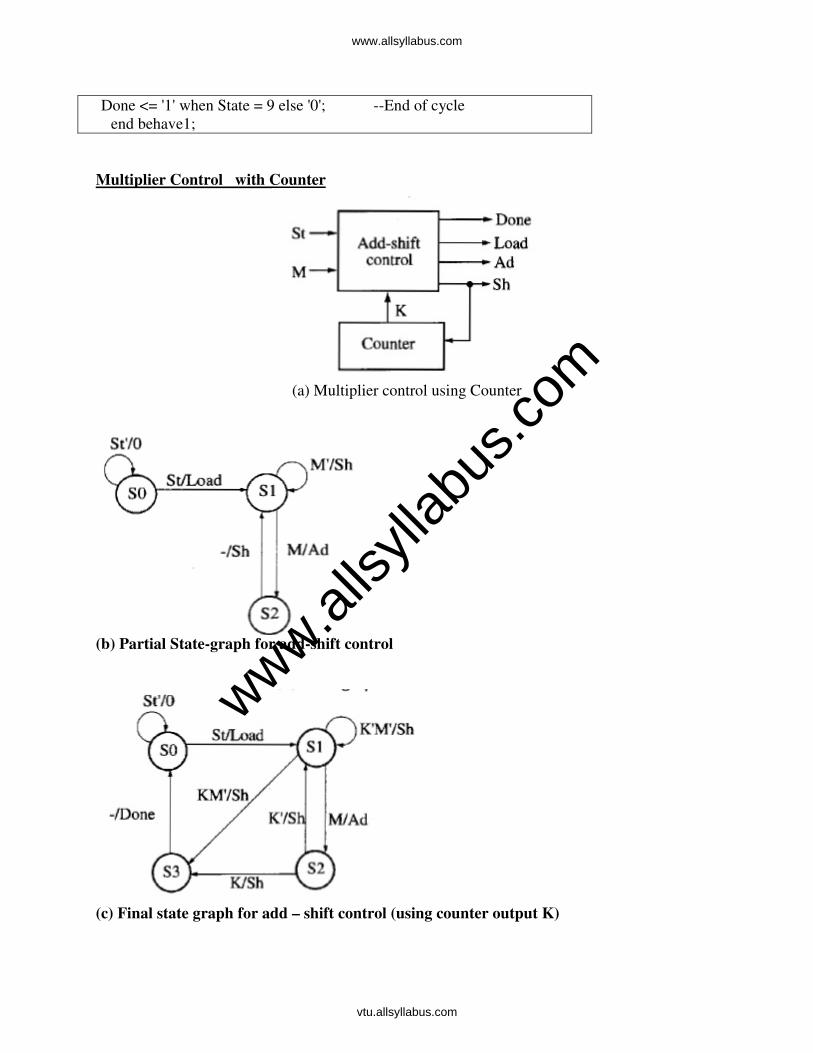
Multiplier Control with Counter
(a) Multiplier control using Counter
(b) Partial State-graph for add-shift control
(c) Final state graph for add – shift control (using counter output K)
www.alls
yllab
us.co
m
www.allsyllabus.com
vtu.allsyllabus.com

Operation of Multiplier using a Counter
Time State CounterProduct
Register
St M K Load Ad Sh Done
t0 S0 00 000000000 0 0 0 0 0 0 0
t1 S0 00 000000000 1 0 0 1 0 0 0
t2 S1 00 000001011 0 1 0 0 1 0 0
t3 S2 00 011011011 0 1 0 0 0 1 0
t4 S1 01 001101101 0 1 0 0 1 0 0
t5 S2 01 100111101 0 1 0 0 0 1 0
t6 S1 10 010011110 0 0 0 0 0 1 0
t7 S1 11 001001111 0 1 1 0 1 0 0
t8 S2 11 100011111 0 1 1 0 0 1 0
t9 S3 00 010001111 0 1 0 0 0 0 1
VHDL code for the binary Multiplier (Control circuit with Counter)
architecture behave2 of mult4X4 is
signal ACC: bit_vector(8 downto 0); --accumulator
alias M: bit is ACC(0); --M is bit 0 of ACC
signal cnt: bit_vector(2 downto 0) ;
begin
process (st)
begin
if St='1' then
cnt<= “000”;
ACC(8 downto 4) <= "00000"; --Begin cycle
ACC(3 downto 0) <= Mplier; --load the multiplier
end if;
end process;
process (clk)
begin
while (cnt < “100”) loop
if (clk=’1’ and clk’event) then
if (M = '1' )then --Add multiplicand
ACC(8 downto 4) <=add4(ACC(7 downto 4),Mcand,'0');
end if;
ACC <= '0' & ACC(8 downto 1); --Shift accumulator right
cnt<=cnt +’1’;
end if;
www.alls
yllab
us.co
m
www.allsyllabus.com
vtu.allsyllabus.com
end loop; end process;
Done <=’1’when cnt=“100”; else “0”;
end behave2;
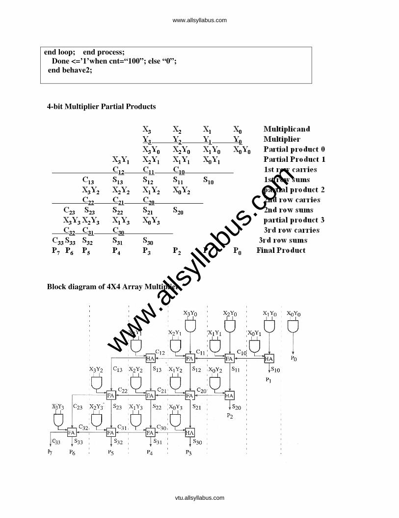
4-bit Multiplier Partial Products
Block diagram of 4X4 Array Multiplier
www.alls
yllab
us.co
m
www.allsyllabus.com
vtu.allsyllabus.com

Operation
• n bit x n bit multiplication would require n2 AND gates, n(n-2) full adders and n
half-adders.
• Number of components increases quadilaterally.
• Longest path goes through 2n adders and the worst case multiply time is 2ntad+tg
where tad delay through an adder and tg is the longest AND gate delay.
• The serial-parallel multiplier requires 2n clocks to complete the multiplication
under worst case. The minimum clock period is determined by the propagation
delay through the n-bit adder as well as the propagation delay and setup time for
accumulator flip flops.
Signed binary numbers - Multiplication
• Complement multiplier if negative.
• Complement multiplicand if negative.
• Multiply the two positive binary numbers.
• Complement the product if negative.
Any other way??
Multiplication of Signed Binary Numbers
• complement the multiplicand
• Complementation of the multiplier or product is not necessary
• 2’s complement of the negative numbers
• Examples: 0.101 +5/8 1.011 -5/8
When multiplying signed binary numbers, we must consider four cases:
www.alls
yllab
us.co
m
www.allsyllabus.com
vtu.allsyllabus.com

Binary Multiplication
Example 1 (Positive Number X Positive Number):
0.1 1 1 (+7/8) ← Multiplicand
X 0.1 0 1 (+5/8) ← Multiplier
(0. 0 0) 0 1 1 1 (+7/64)
(0. )0 1 1 1 (+7/16)
0. 1 0 0 0 1 1 (+35/64)
Note: The proper representation of the fractional partial products requires extension of
the sign bit past the binary point, as indicated in parentheses. (such extension is not
necessary in the hardware.)
Example 2 (negative Number X Positive Number):
1 . 1 0 1 (-3/8)
X 0 . 1 0 1 (+5/8)
(1. 1 1) 1 1 0 1 (-3/64)
(1. )1 1 0 1 (-3/16)
_____________________________
1. 1 1 0 0 0 1 (-15/64)
Note: The extension of the sign bit provides proper representation of the negative products.
Example 3 (Positive Number X negative Number):
0 . 1 0 1 (+5/8)
X 1 . 1 0 1 (-3/8)
_____________________________
(0. 0 0) 0 1 0 1 (+5/64)
(0.) 0 1 0 1 ((+5/16)
(0.) 0 1 1 0 0 1
1. 0 1 1 (-5/8) ���� Note: The 2’s complement of the multiplicand is added at this point
1. 1 1 0 0 0 1 (-15/64)
Example 4 (negative Number X negative Number):
1 . 1 0 1 (-3/8)
X 1 . 1 0 1 (-3/8)
(1. 1 1) 1 1 0 1
(1.) 1 1 0 1
(1.) 1 1 0 0 0 1
0. 0 1 1 (+3/8)
0. 0 0 1 0 0 1 (+9/64)
Preserve sign bit while extension and add the 2’s complement of the multiplicand.
www.alls
yllab
us.co
m
www.allsyllabus.com
vtu.allsyllabus.com

Procedure
The procedure for multiplying signed 2’s complement binary fractions:
• Preserve the sign of the partial product at each step
• If the sign of the multiplier is negative, complement the multiplicand before adding
it in at the last step.
• The hardware is almost identical to that used for multiplication of positive numbers,
except a complementer must be added for the multiplicand.
Block diagram for 2’s Complement Multiplier
Operation
• 5-bit adder is used so that sign bit is not lost due to a carry into sign bit position.
• M is current active bit of the multiplier.
• Sh causes accumulator to shift right by one bit with sign extension.
• Ad causes adder output to be loaded into accumulator. Carry bit is discarded since
we are doing 2’s complement addition.
• Cm causes multiplicand to be complemented before it is given to adder input. It is
also connected as carry input to adder. So that Cm=1, it gives us two’s complement.
www.alls
yllab
us.co
m
www.allsyllabus.com
vtu.allsyllabus.com

State Graph for 2’s Complement Multiplier
-/Sh
-/Sh
-/Sh
M/Ad M/Ad
M/Cm Ad
M/Ad
St/Load
-/Done
M’/Sh
M’/Sh
M’/Sh
M’/0
S0
S8
S7
S6
S5 S4
S3
S2
S1
St’/0
www.alls
yllab
us.co
m
www.allsyllabus.com
vtu.allsyllabus.com

Block diagram for Faster Multiplier
State Graph for Faster Multiplier
www.alls
yllab
us.co
m
www.allsyllabus.com
vtu.allsyllabus.com

VHDL Code --Behavioral Model for 2’s Complement Multiplier
library BITLIB;
use BITLIB.bit_pack.all;
entity mult2C is
port (CLK, St: in bit;
Mplier,Mcand : in bit_vector(3 downto 0);
Product: out bit_vector (6 downto 0);
Done: out bit);
end mult2C;
architecture behave1 of mult2C is
signal State : integer range 0 to 5;
signal A, B: bit_vector(3 downto 0);
alias M: bit is B(0);
begin
process
variable addout: bit_vector(4 downto 0);
begin
wait until CLK = '1';
case State is
when 0=> --initial State
if St='1' then
A <= "0000"; --Begin cycle
B <= Mplier; --load the multiplier
State <= 1;
end if;
when 1 | 2 | 3 => --"add/shift" State
if M = '1' then
addout := add4(A,Mcand,'0'); --Add multiplicand to A and shift
A <= Mcand(3) & addout(3 downto 1);
B <= addout(0) & B(3 downto 1);
else
A <= A(3) & A(3 downto 1); --Arithmetic right shift
B <= A(0) & B(3 downto 1);
end if;
State <= State + 1;
when 4 => --add complement if sign bit
if M = '1' then --of multiplier is 1
addout := add4(A, not Mcand,'1');
A <= not Mcand(3) & addout(3 downto 1);
B <= addout(0) & B(3 downto 1);
else
A <= A(3) & A(3 downto 1); --Arithmetic right shift
B <= A(0) & B(3 downto 1);
www.alls
yllab
us.co
m
www.allsyllabus.com
vtu.allsyllabus.com

end if;
State <= 5;
wait for 0 ns;
Done <= '1';
Product <= A(2 downto 0) & B; --output product
when 5 =>
State <= 0;
Done <= '0';
end case;
end process;
end behave1;
Test Bench for Signed Multiplier
To test the multiplier, need to test the
• 4 standard cases( ++, +-, -+, --)
• Special & limiting cases – including 0, largest positive fraction, most
negative fraction, all 1’s.
The test bench program below supplies a sequence of values for the multiplicand,
multiplier, the clock and start signal.
VHDL Program -- Test Bench for Signed Multiplier
library BITLIB;
use BITLIB.bit_pack.all;
entity testmult is
end testmult;
architecture test1 of testmult is
component mult2C
port(CLK, St: in bit;
Mplier,Mcand : in bit_vector(3 downto 0);
Product: out bit_vector (6 downto 0);
Done: out bit);
end component;
constant N: integer := 11;
type arr is array(1 to N) of bit_vector(3 downto 0);
www.alls
yllab
us.co
m
www.allsyllabus.com
vtu.allsyllabus.com

constant Mcandarr: arr := ("0111", "1101", "0101", "1101", "0111", "1000",
"0111", "1000", "0000", "1111", "1011");
constant Mplierarr: arr := ("0101", "0101", "1101", "1101", "0111", "0111",
"1000", "1000", "1101", "1111", "0000");
signal CLK, St, Done: bit;
signal Mplier, Mcand: bit_vector(3 downto 0);
signal Product: bit_vector(6 downto 0);
begin
CLK <= not CLK after 10 ns;
process
begin
for i in 1 to N loop
Mcand <= Mcandarr(i);
Mplier <= Mplierarr(i);
St <= '1';
wait until rising_edge(CLK);
St <= '0';
wait until falling_edge(Done);
end loop;
end process;
mult1: mult2c port map(Clk, St, Mplier, Mcand, Product, Done);
end test1;
VHDL Model for 2’s complement Multiplier with Control Signals (uses a separate process
for the combinational logic and does all of the register updates in another process)
library BITLIB;
use BITLIB.bit_pack.all;
entity mult2Cs is
port (CLK, St: in bit;
Mplier,Mcand : in bit_vector(3 downto 0);
Product: out bit_vector (6 downto 0);
Done: out bit);
end mult2Cs;
-- This architecture of a 4-bit multiplier for 2's complement numbers uses control signals.
architecture behave2 of mult2Cs is
signal State, Nextstate: integer range 0 to 5;
signal A, B: bit_vector(3 downto 0);
signal AdSh, Sh, Load, Cm: bit;
signal addout: bit_vector(4 downto 0);
alias M: bit is B(0);
www.alls
yllab
us.co
m
www.allsyllabus.com
vtu.allsyllabus.com

begin
process (state, st, M)
begin
Load <= '0'; AdSh <= '0'; Sh <= '0'; Cm <= '0'; Done <= '0';
case State is
when 0=> --initial State
if St='1' then Load <= '1'; Nextstate <= 1; end if;
when 1 | 2 | 3 => --"add/shift" State
if M = '1' then AdSh <= '1';
else Sh <= '1';
end if;
Nextstate <= State + 1;
when 4 => --add complement if sign
if M = '1' then --bit of multiplier is 1
Cm <= '1'; AdSh <= '1';
else Sh <= '1';
end if;
nextstate <= 5;
when 5 => --output product
done <= '1';
nextstate <= 0;
end case;
end process;
addout <= add4(A, Mcand, '0') when Cm = '0'
else add4(A, not Mcand, '1');
process
begin
wait until CLK = '1'; --executes on rising edge
if Load = '1' then --load the multiplier
A <= "0000";
B <= Mplier;
end if;
if AdSh = '1' then --Add multiplicand to A and shift
A <= (Mcand(3) xor Cm) & addout(3 downto 1);
B <= addout(0) & B(3 downto 1);
end if;
if Sh = '1' then
A <= A(3) & A(3 downto 1);
B <= A(0) & B(3 downto 1);
end if;
State <= Nextstate;
end process;
Product <= A(2 downto 0) & B;
end behave2;
www.alls
yllab
us.co
m
www.allsyllabus.com
vtu.allsyllabus.com

Design of the control circuit in a Multiplier using a counter (74163)
Fig below shows the control circuit using a counter.
The counter output Q3Q2Q1Q0 represents the 6 states of the counter with the state
assignment S0 -> 0000, S1 ���� 0100, S2 ���� 0101, S3 ����0110, S4 ���� 0111, S5 ����1000
Counter is cleared in S5, loaded with Din = 0100 in S0 & incremented in remaining states.
The design is given below:
VHDL model of a 4-bit multiplier for 2's complement numbers
WHICH implements the controller using a counter and logic equations.
library BITLIB;
use BITLIB.bit_pack.all;
entity mult2CEQ is
port(CLK, St: in bit;
Mplier,Mcand: in bit_vector(3 downto 0);
www.alls
yllab
us.co
m
www.allsyllabus.com
vtu.allsyllabus.com

Product: out bit_vector(6 downto 0));
end mult2CEQ;
architecture m2ceq of mult2CEQ is
signal A, B, Q, Comp: bit_vector(3 downto 0);
signal addout: bit_vector(4 downto 0);
signal AdSh, Sh, Load, Cm, Done, Ld1, CLR1, P1: bit;
Signal One: bit:='1';
Signal Din: bit_vector(3 downto 0) := "0100";
alias M: bit is B(0);
begin
Count1: C74163 port map (Ld1, CLR1, P1, One, CLK, Din, open, Q);
P1 <= Q(2);
CLR1 <= not Q(3);
Done <= Q(3);
Sh <= not M and Q(2);
AdSh <= M and Q(2);
Cm <= Q(1) and Q(0) and M;
Load <= not Q(3) and not Q(2) and St;
Ld1 <= not Load;
Comp <= Mcand xor (Cm & Cm & Cm & Cm); --complement Mcand if
Cm='1'
addout <= add4(A,Comp,Cm); --add complementer output to A
process
begin
wait until CLK = '1'; --executes on rising edge
if Load = '1' then --load the multiplier
A <= "0000";
B <= Mplier;
end if;
if AdSh = '1' then --Add multiplicand to A and shift
A <= (Mcand(3) xor Cm) & addout(3 downto 1);
B <= addout(0) & B(3 downto 1);
end if;
if Sh = '1' then --Right shift with sign extend
A <= A(3) & A(3 downto 1);
B <= A(0) & B(3 downto 1);
end if;
if Done = '1' then
Product <= A(2 downto 0) & B;
end if;
end process;
end m2ceq;
www.alls
yllab
us.co
m
www.allsyllabus.com
vtu.allsyllabus.com

Binary Divider
Procedure:
Block Diagram for Parallel Binary Divider
Sequence of functions:
� A shift signal (Sh) will shift the dividend one place to the left.
� A subtract signal (Su) will subtract the divisor from the 5 leftmost bits in the
dividend register and set the quotient bit (the rightmost bit in the dividend register)
to 1.
Sh
0
C
Su
St (Start Signal)
V
(Overflow Indicator)
Dividend Register
Y3 Y2 Y1 Y0
X8 X7 X6 X5 X4 X3 X2 X1 X0 Sh Ld
Subtractor and comparator Control
Clock www.alls
yllab
us.co
m
www.allsyllabus.com
vtu.allsyllabus.com

� If the divisor is greater than the 4 leftmost dividend bits, the comparator output is
C=0; otherwise, C=1.
� The control circuit generates the required sequence of shift and subtract signals.
Whenever C=0, subtraction can not occur, so a shift signal is generated and quotient
bit is set to 0.
� Whenever C=1, a subtraction signal is generated, and the quotient bit is set to 1.
Example (135 / 13):
www.alls
yllab
us.co
m
www.allsyllabus.com
vtu.allsyllabus.com

Overflow
• As a result of a division operation, If the quotient contains more bits than are
available for storing the quotient, we say that an overflow has occurred.
• It is not necessary to carry out the division if an overflow condition exists.
• An initial comparison of the dividend and divisor determine whether the quotient
will be too large or not.
Detection of Overflow
State Diagram for Divider Control Circuit
Operation of the Divider
• When a start signal (St) occurs, the 8-bit dividend and 4-bit divisor are loaded into
the appropriate registers
• If C is 1, the quotient would require five or more bits. Since space is only provided
for 4-bit quotient, this condition constitutes an overflow, so the divider is stopped
and the overflow indicator is set by the V output.
• Normally, the initial value of C is 0, so a shift will occur first, and the control circuit
will go to state S2.
www.alls
yllab
us.co
m
www.allsyllabus.com
vtu.allsyllabus.com

• Then, if C=1, subtraction occurs. After the subtraction is completed, C will always
be 0, so the next clock pulse will produce a shift.
• This process continues until four shifts have occurred and the control is in state S5.
• Then a final subtraction occurs if necessary, and the control returns to the stop
state. For this example, we will assume that when the start signal (St) occurs, it will
be 1 for one clock time, and then it will remain 0 until the control network is back in
state S0. Therefore, St will always be 0 in states S1through S5.
www.alls
yllab
us.co
m
www.allsyllabus.com
vtu.allsyllabus.com

Question 4.5 (a) Draw the block diagram for divider for unsigned binary number that
divides an 8 bit dividend by a 3 bit divisor to give a 5 bit quotient
(b) Draw state graph for the control circuit, assume that the start signal (st) is
present for 1 clock period.
(c) Write VHDL description of the divider.
(a) Block diagram for divider for unsigned binary number
(b) Refer State Diagram for Divider Control Circuit
(c) VHDL description of the divider:
library ieee;
use ieee.std_logic_1164.all;
entity divider is
port (St, Clk: in std_logic;
dend: in std_logic_vector(7 downto 0);
dsor: in std_logic_vector(2 downto 0);
v: out std_logic;
qent: out std_logic_vector(4 downto 0));
end divider;
architecture beh of divider is
signal C, Sh, su, Ld: std_logic;
signal DendR: std_logic_vector(8 downto 0);
signal DsorR: std_logic_vector(2 downto 0);
Load
Sh
0
C
Su
St
V
Dividend Register
Y2 Y1 Y0
X8 X7 X6 X5 X4 X3 X2 X1 X0
Subtractor and comparator
Control
Clock
www.alls
yllab
us.co
m
www.allsyllabus.com
vtu.allsyllabus.com

signal Sub: std_logic_vector(4 downto 0);
signal State, nxState: integer range 0 to 6;
begin
Sub <= Add4 (DendR(8 downto 5), not(‘0’ & DsorR), ‘1’);
C<=sub(4);
Qent<=DendR(4 downto 0);
Process (state, st, C)
Begin
V<= ‘0’; Sh<= ‘0’; Su<=’0’; Ld<=’0’;
Case state is
When 0=> if (St=’1’) then Ld<=’1’; nxState<=’1’;
Else nxstate<=’0’; end if;
When 1=> if(C=’1’) then V<=’1’; nxstate<=’0’;
Else Sh<=’1’; nxState<=2; end if;
When 2|3|4|5 => if (C=’1’) then Su<=’1’; nxstate<=State;
Else Sh<=’1’; nxstate<=state + 1; end if;
When 6 => if (C=’1’) then Su<=’1’; end if;
nxState<=’0’;
end case;
end process;
process (Clk)
begin
if (Clk=’1’ and Clk’event) then
state<=nxState;
if (Ld=’1’) then
DendR<=’0’ & dend;
DsorR<=dsor; end if;
If (Sh=’1’) then
DendR<= DendR (7 downto 0) & ‘0’; end if;
If (Su=’1’) then
DendR(8 downto 5) <=sub(3 downto 0);
DendR(0)<=’1’; end if;
End if;
End process;
End divider; www.a
llsyll
abus
.com
www.allsyllabus.com
vtu.allsyllabus.com

Block diagram for Signed Divider
Signals
LdU Load upper half of dividend from bus.
LdL Load lower half of dividend from bus.
Lds Load sign of dividend into sign flip-flop.
S Sign of dividend.
Cml Complement dividend register(2’s complement)
Ldd Load divisor from bus
Su Enable adder output onto bus (Ena) and load upper half of
dividend from bus.
Cm2 Enable complementer. (Cm2 equals the complement of the sign bit of the divisor, so
a positive divisor is complemented and a negative divisor is not.)
Sh Shift the dividend register left one place and increment the counter
Dbus Data in
Ldd
Dividend
C
Ena
Compout
Cm2
Cm2
Cm1
Ldu Ld1
Sh
Lds
K
16 16
16 16
16
16
16
St
V
S
Acc(Remainder) Q(Quotient)
16-bit Full Adder Cin
16-bit Complementor
Divisor
Main Control
4-bit Counter
Sign
Cout
www.alls
yllab
us.co
m
www.allsyllabus.com
vtu.allsyllabus.com
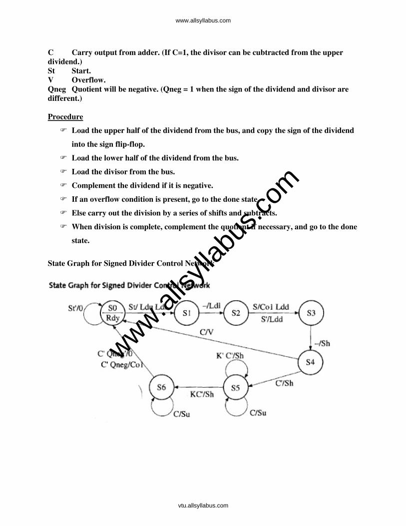
C Carry output from adder. (If C=1, the divisor can be cubtracted from the upper
dividend.)
St Start.
V Overflow.
Qneg Quotient will be negative. (Qneg = 1 when the sign of the dividend and divisor are
different.)
Procedure
� Load the upper half of the dividend from the bus, and copy the sign of the dividend
into the sign flip-flop.
� Load the lower half of the dividend from the bus.
� Load the divisor from the bus.
� Complement the dividend if it is negative.
� If an overflow condition is present, go to the done state.
� Else carry out the division by a series of shifts and subtracts.
� When division is complete, complement the quotient if necessary, and go to the done
state.
State Graph for Signed Divider Control Network
www.alls
yllab
us.co
m
www.allsyllabus.com
vtu.allsyllabus.com

VHDL Model of 32-bit Signed Divider
library BITLIB;
use BITLIB.bit_pack.all;
entity sdiv is
port(Clk,St: in bit;
Dbus: in bit_vector(15 downto 0);
Quotient: out bit_vector(15 downto 0);
V, Rdy: out bit);
end sdiv;
architecture Signdiv of Sdiv is
constant zero_vector: bit_vector(31 downto 0):=(others=>'0');
signal State: integer range 0 to 6;
signal Count : integer range 0 to 15;
signal Sign,C,NC: bit;
signal Divisor,Sum,Compout: bit_vector(15 downto 0);
signal Dividend: bit_vector(31 downto 0);
alias Q: bit_vector(15 downto 0) is Dividend(15 downto 0);
alias Acc: bit_vector(15 downto 0) is Dividend(31 downto 16);
begin -- concurrent statements
compout <= divisor when divisor(15) = '1' -- 1's complementer
else not divisor;
Addvec(Acc,compout,not divisor(15),Sum,C,16); -- 16-bit adder
Quotient <= Q;
Rdy <= '1' when State=0 else '0';
process
begin
wait until Clk = '1'; -- wait for rising edge of clock
case State is
when 0=>
if St = '1' then
Acc <= Dbus; -- load upper dividend
Sign <= Dbus(15);
State <= 1;
V <= '0'; -- initialize overflow
Count <= 0; -- initialize counter
end if;
when 1=>
Q <= Dbus; -- load lower dividend
State <= 2;
when 2=>
Divisor <= Dbus;
if Sign ='1'then -- two's complement Dividend if necessary
addvec(not Dividend,zero_vector,'1',Dividend,NC,32);
www.alls
yllab
us.co
m
www.allsyllabus.com
vtu.allsyllabus.com

end if;
State <= 3;
when 3=>
Dividend <= Dividend(30 downto 0) & '0'; -- left shift
Count <= Count+1;
State <= 4;
when 4 =>
if C ='1' then -- C
v <= '1';
State <= 0;
else -- C'
Dividend <= Dividend(30 downto 0) & '0'; -- left shift
Count <= Count+1;
State <= 5;
end if;
when 5 =>
if C = '1' then -- C
ACC <= Sum; -- subtract
Q(0)<= '1';
else
Dividend <= Dividend(30 downto 0) & '0'; -- left shift
if Count = 15 then -- KC'
count<= 0; State <= 6;
else Count <= Count+1;
end if;
end if;
when 6=>
if C = '1' then -- C
Acc <= Sum; -- subtract
Q(0) <= '1';
else if (Sign xor Divisor(15))='1' then -- C'Qneg
addvec(not Dividend,zero_vector,'1',Dividend,NC,32);
end if; -- 2's complement Dividend
state <= 0;
end if;
end case;
end process;
end signdiv;
Steps followed:
Since the 1’s complementer and adder are combinational networks, their operations are
represented by concurrent statements.
ADDVEC is executed any time ACC or compout changes, so Sum and carry are
immediately recomputed.
www.alls
yllab
us.co
m
www.allsyllabus.com
vtu.allsyllabus.com

All the signals that represent register outputs are updated on the rising edge of the clock.
For example, ADDVEC is called in states 2 and 6 to store the 2’s complement of the
dividend back into the dividend register.
The counter is simulated by an integer signal, count.
www.alls
yllab
us.co
m
www.allsyllabus.com
vtu.allsyllabus.com
Related Documents