Welcome message from author
This document is posted to help you gain knowledge. Please leave a comment to let me know what you think about it! Share it to your friends and learn new things together.
Transcript


32
by Barry Olney
The Plain Truth About Plane Jumpers
SUMMARY: The key to building the optimum board stackup is determining how and where the return currents flow. But it is also just as important to have the board constructed to your specifications – having engineering drive fabrication – rather than delegating impedance control and material selection to the fab shop.
Moats, islands, cut-outs in the ground plane, isolated power planes, floating ground regions, and a host of other intricate layout techniques are often used by PCB designers to reduce cross-talk, EMI, and to otherwise improve overall system performance.
But a high-speed signal crossing a split in the plane causes problems along at least three dimensions, including signal quality, crosstalk, and EMI. The problem is the imped-ance discontinuity in the signal path crossing the split. The discontinuity reflects energy back toward the source – particularly the higher-fre-quency components of the signal. At high fre-quencies, the return current follows the path of least inductance – which is directly below the signal trace – but that path is broken by the split. The reason for this discontinuity is the fact that the return current has to find an al-ternate path back to the source, creating a large loop area and a nice little antenna for differen-tial-mode radiation.
It is important to keep in mind that both ground and power planes (any plane) can be used as the reference plane and return current path for a signal.
The key to a successful mixed digital/analog design is functional partitioning, understand-ing the current return path, and routing con-trol and management – not carving up ground planes. It is always better to have just one single reference (ground) plane for a system.
I mentioned “plane jumpers” briefly in my recent column Mixed Digital Analog Technol-ogies, where I said: “If a digital signal(s) must
cross a split in the power refer-ence plane a ‘plane jumper’ decou-
pling capacitor (100nF) can be placed close to the offending signal(s) to provide a
path for the return current between the two supplies (e.g., 3.3V —||— 1.5V).”
In Figure 1, the gap totally isolates the pow-er reference planes, so a plane jumper capaci-tor is used to allow the return current to bridge the gap in the planes from 3.3V to 1.5V. This is quite effective, but should be only used as a last resort, if you cannot avoid routing such a signal across the gap. I must say that it does look weird – having a decap on the schematic between 3.3V and 1.5V, where decaps are nor-mally placed between power and ground.
Figure 1:
BEYOND DESIGN
column
34
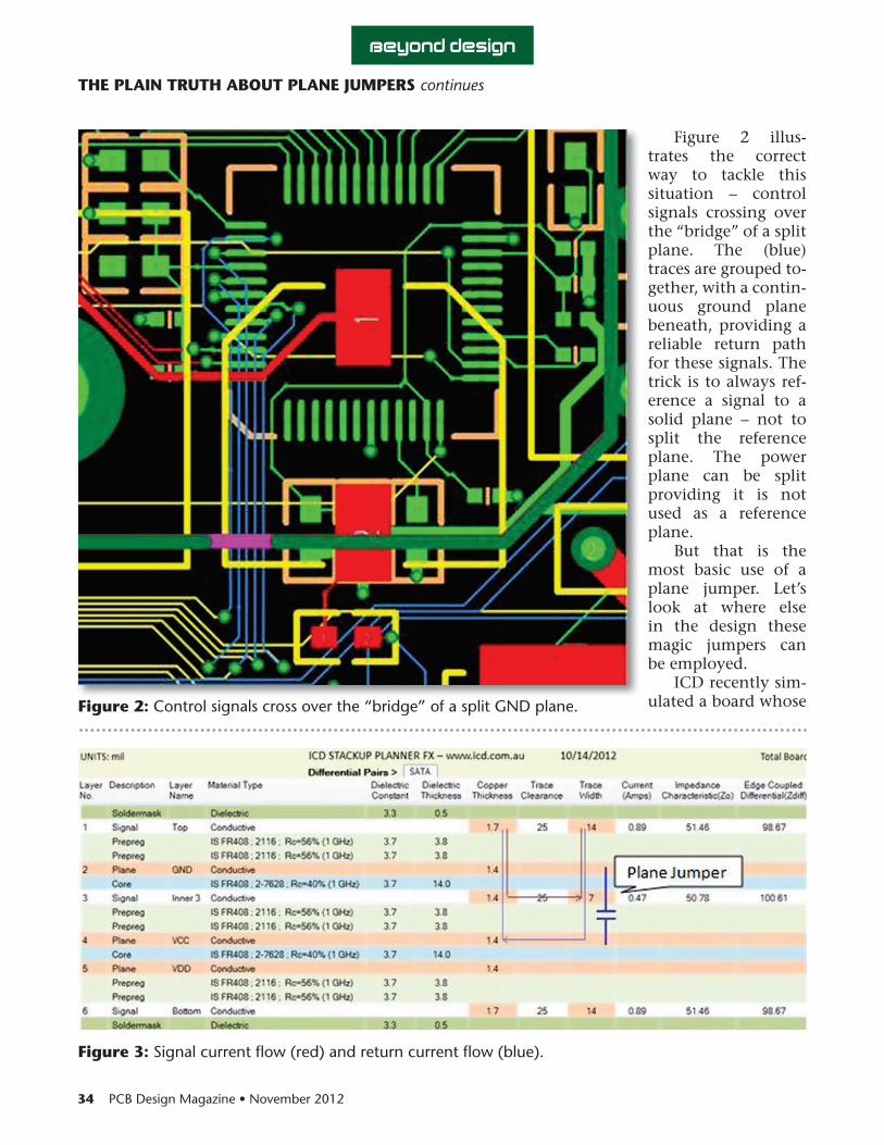
Figure 2 illus-trates the correct way to tackle this situation – control signals crossing over the “bridge” of a split plane. The (blue) traces are grouped to-gether, with a contin-uous ground plane beneath, providing a reliable return path for these signals. The trick is to always ref-erence a signal to a solid plane – not to split the reference plane. The power plane can be split providing it is not used as a reference plane.
But that is the most basic use of a plane jumper. Let’s look at where else in the design these magic jumpers can be employed.
ICD recently sim-ulated a board whose Figure 2:
Figure 3:
Beyond design
THE PLAIN TRUTH ABOUT PLANE JUMPERS continues

35
THE PLAIN TRUTH ABOUT PLANE JUMPERS continues
designers intended to route high-speed signals from a chip to a connector on top of the board. The routing fanned out from the BGA, went di-rectly to layer 3, then popped back up through a via to a connector on the top layer. This seems perfectly reasonable.
But looking at the stackup in more detail, the signal was first referenced to the GND plane on layer 2; then, as it transitioned to layer 3, its reference plane changed to VCC (layer 4) due to proximity. There is, in this case, only one way for the return current to “jump” planes, and that is by finding the nearest VCC to GND decou-pling capacitor – which may be a long distance (relatively) from the signal transient, creating a large loop area and undesirable common-mode currents. This can all be avoided by placing a plane jumper (decap), close to the signal-via transition, between VCC and GND.
In the case, where there are multiple ground planes on a PCB, we cannot simply assume that “ground is ground” and be sure that the return current will find its way back to the source. GND stitching vias should be placed next to each sig-nal-via transition to stitch the GND planes to-gether, providing a clear return path.
Now, the designer had good intentions: us-ing the GND plane on layer 2 as the common reference plane. Everything would be fine, un-til a lack of communication (and understanding of the design parameters) led the CAM engineer
at the fabricator to change the thickness of the core and pre-preg materials to suit the dielectric materials they had in stock.
This is a classic case that we see all the time. It is the point where our design crosses over into the real world – manufacturing. It represents a point beyond which many designers rarely dare to venture, due to their lack of understanding of PCB fabrication processes. But, it is a fact that the more awareness we have surrounding the fabrication processes, the better our designs be-come, and the better designers we become.
The CAM professional looks at your board in purely physical terms. He, most likely, has no understanding of which signals are critical, and your current return paths. His window to your world consists of layers of dielectric materi-als, copper foils, PTH vias, and soldermasks. The standard Gerber file format – transferred from layout to fab – is a rather primitive (based on the old X,Y plotters) but highly effective format for describing two-dimensional graphical informa-tion. It is well suited for representing the two major components of a PCB image: lines and dots. But this is all they are to the CAM engineer.
The proverbial ”left shift” in the design pro-cess is to put control of the stackup build back into the hands of engineers and PCB designers – enabling them to collaborate with, if not con-trol, the outcome of the fabrication. To do this, designers need a comprehensive list of standard
Figure 4:
Beyond design

36
dielectric materials from popular manufacturers like Isola, Nelco, Rogers, etc., and the ability to insert these into a prototype stackup, determin-ing the single-ended and differential impedanc-es of these materials combined with PCB layout design rules. The ICD Stackup Planner, shown in Figures 3 and 4 (available for download at www.icd.com.au) handles these tasks quite well, in fact, providing an interface between CAM, signal-integrity simulation, and PCB layout.
Since layer 3 is now closer to the GND plane on layer 2 in Figure 4, it will be used for the current return path, rather than VCC, as be-fore. And, there is no need for plane jumpers in this case. This is by far the best scenario. The PCB designer can pass this information on to fabrication with confidence that his intended stackup build will be manufactured to suit the design’s electrical needs.
Plane jumpers can be used to easily resolve a return-current issue, but they are best avoid-ed by taking control of the stackup back into the hands of the hardware engineer and PCB designer, while streamlining communication between the hardware-engineering team and fabrication.
Points to Remember
discontinuity in the signal path crossing the split, creating signal reflections, cross- talk, and unwanted common-mode currents that can lead to EMI problems.
can be used as a reference plane and return current-return path for a signal.
reference (ground) plane for a system.
provide a path for the return current between the two supply planes.
is best used for control signals to cross a split plane.
to a via to allow the flow of return current from plane to plane.
ground-stitching vias should be placed next to each signal-via transition.
of the fabrication processes, the better the outcome of our design, and the better designers we become.
put control of the stackup back into the hands of hardware designer so that electrical design parameters don’t get pushed to the side. PCBDESIGN
References1. “Advanced Design for SMT” two-day
course – Barry Olney2. Beyond Design: The Dumping Ground –
Barry Olney3. Intro to Board-Level Simulation and the
PCB Design Process– Barry Olney4. PCB Design Techniques for DDR, DDR2 &
DDR3, Part 1 – Barry Olney 5. PCB Design Techniques for DDR, DDR2 &
DDR3, Part 2 – Barry Olney6. Electromagnetic Compatibility Engineer-
ing – Henry Ott7. High-Speed Digital Design – Howard
Johnson8. The ICD Stackup Planner and PDN Plan-
ner can be downloaded from www.icd.com.au
THE PLAIN TRUTH ABOUT PLANE JUMPERS continues
Beyond design
Related Documents