Mathematics and Computers in Simulation 71 (2006) 256–269 Stability analysis of a single inductor dual switching dc–dc converter L. Benadero a,∗ , R. Giral b , A. El Aroudi b , J. Calvente b a Dep. F´ ısica Aplicada, Universitat Polit` ecnica de Catalunya (UPC), Campus Nord UPC, 08034 Barcelona, Spain b Dep. d’Enginyeria Electr ` onica, El` ectrica i Autom´ atica, Universitat Rovira i Virgili (URV), Campus Sescelades, Tarragona, Spain Available online 17 April 2006 Abstract This paper deals with the analysis of a single inductor switching dc–dc power electronics converter which is used to regulate two, in general non-symmetric, positive and negative outputs. A PWM control with a double PI feedback loop is used for the regulation of both output voltages. The steady state properties of this converter are first discussed and then stability is studied in terms of both power stage and control parameters. © 2006 IMACS. Published by Elsevier B.V. All rights reserved. Keywords: Dual converter; PWM control; PI feedback loop; Single inductor; Stability analysis 1. Introduction The proposed dual switching converter for automotive applications in [9], is a single inductor dc–dc converter able to regulate two (positive and negative) symmetric outputs. Because in general it can be controlled by two independent inputs so as to provide two, not necessarily symmetric, voltages, this is a third order multiple-input multiple-output (MIMO) structure (in fact two-input two-output). Transitions between different topologies due to the switching action make dc–dc converters to be variable structure systems (VSS) [2,4], a class of non-linear dynamical systems with specific questions due to their non-smooth character. An extensive literature is devoted to complex dynamics arising in these devices [6,3,21]. Non-linear analysis has also been extended to dual dc–dc converters, for instance [7,8,11,18] for symmetric behaviour and [12] for the asymmetric case. What is a special feature of [9] is the use of a single inductor that transfers energy from an unregulated source to both loads. Two feedback loops are used to regulate both output voltages by means of pulse width modulated (PWM) techniques [13,14,17], thus controlling the switching time intervals. This paper is organised as follows. Firstly, the scheme of the circuit is described in Section 2 and the switched model is built up in Section 3. The main characteristic relations between averaged state variables and duty cycles are given in Section 4. Finally, an explicit expression for the Jacobian and some representative results concerning stability are derived in Section 5. ∗ Corresponding author. E-mail addresses: [email protected] (L. Benadero), [email protected] (A.E. Aroudi). 0378-4754/$32.00 © 2006 IMACS. Published by Elsevier B.V. All rights reserved. doi:10.1016/j.matcom.2006.02.009

Welcome message from author
This document is posted to help you gain knowledge. Please leave a comment to let me know what you think about it! Share it to your friends and learn new things together.
Transcript

Mathematics and Computers in Simulation 71 (2006) 256–269
Stability analysis of a single inductor dualswitching dc–dc converter
L. Benadero a,∗, R. Giral b, A. El Aroudi b, J. Calvente b
a Dep. Fısica Aplicada, Universitat Politecnica de Catalunya (UPC), Campus Nord UPC, 08034 Barcelona, Spainb Dep. d’Enginyeria Electronica, Electrica i Automatica, Universitat Rovira i Virgili (URV), Campus Sescelades, Tarragona, Spain
Available online 17 April 2006
Abstract
This paper deals with the analysis of a single inductor switching dc–dc power electronics converter which is used to regulate two,in general non-symmetric, positive and negative outputs. A PWM control with a double PI feedback loop is used for the regulationof both output voltages. The steady state properties of this converter are first discussed and then stability is studied in terms of bothpower stage and control parameters.© 2006 IMACS. Published by Elsevier B.V. All rights reserved.
Keywords: Dual converter; PWM control; PI feedback loop; Single inductor; Stability analysis
1. Introduction
The proposed dual switching converter for automotive applications in [9], is a single inductor dc–dc converter ableto regulate two (positive and negative) symmetric outputs. Because in general it can be controlled by two independentinputs so as to provide two, not necessarily symmetric, voltages, this is a third order multiple-input multiple-output(MIMO) structure (in fact two-input two-output).
Transitions between different topologies due to the switching action make dc–dc converters to be variable structuresystems (VSS) [2,4], a class of non-linear dynamical systems with specific questions due to their non-smooth character.An extensive literature is devoted to complex dynamics arising in these devices [6,3,21]. Non-linear analysis has alsobeen extended to dual dc–dc converters, for instance [7,8,11,18] for symmetric behaviour and [12] for the asymmetriccase. What is a special feature of [9] is the use of a single inductor that transfers energy from an unregulated source toboth loads. Two feedback loops are used to regulate both output voltages by means of pulse width modulated (PWM)techniques [13,14,17], thus controlling the switching time intervals.
This paper is organised as follows. Firstly, the scheme of the circuit is described in Section 2 and the switched modelis built up in Section 3. The main characteristic relations between averaged state variables and duty cycles are givenin Section 4. Finally, an explicit expression for the Jacobian and some representative results concerning stability arederived in Section 5.
∗ Corresponding author.E-mail addresses: [email protected] (L. Benadero), [email protected] (A.E. Aroudi).
0378-4754/$32.00 © 2006 IMACS. Published by Elsevier B.V. All rights reserved.doi:10.1016/j.matcom.2006.02.009
L. Benadero et al. / Mathematics and Computers in Simulation 71 (2006) 256–269 257
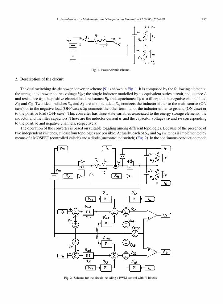
Fig. 1. Power circuit scheme.
2. Description of the circuit
The dual switching dc–dc power converter scheme [9] is shown in Fig. 1. It is composed by the following elements:the unregulated power source voltage VIN; the single inductor modelled by its equivalent series circuit, inductance Land resistance RL; the positive channel load, resistance RP and capacitance CP as a filter; and the negative channel loadRN and CN. Two ideal switches SA and SB are also included: SA connects the inductor either to the main source (ONcase), or to the negative load (OFF case); SB connects the other terminal of the inductor either to ground (ON case) orto the positive load (OFF case). This converter has three state variables associated to the energy storage elements, theinductor and the filter capacitors. These are the inductor current iL and the capacitor voltages vP and vN correspondingto the positive and negative channels, respectively.
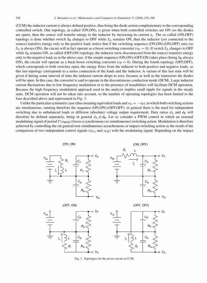
The operation of the converter is based on suitable toggling among different topologies. Because of the presence oftwo independent switches, at least four topologies are possible. Actually, each of SA and SB switches is implemented bymeans of a MOSFET (controlled switch) and a diode (uncontrolled switch) (Fig. 2). In the continuous conduction mode
Fig. 2. Scheme for the circuit including a PWM control with PI blocks.
258 L. Benadero et al. / Mathematics and Computers in Simulation 71 (2006) 256–269
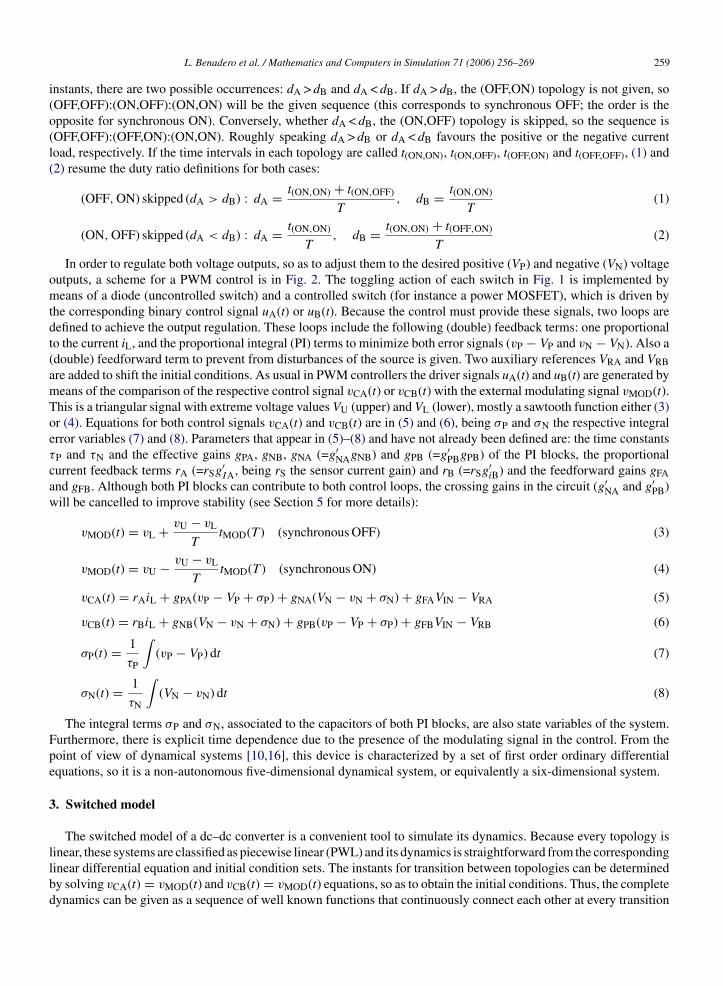
(CCM) the inductor current is always defined positive, thus being the diode action complementary to the correspondingcontrolled switch. One topology, as called (ON,ON), is given when both controlled switches are ON (so the diodesare open), then the source will transfer energy to the inductor by increasing its current iL. The so called (ON,OFF)topology is done whether switch SB changes to OFF while SA remains ON, then the inductor (yet connected to thesource) transfers energy only to the positive load; notice that if the switching sequence (ON,ON):(ON,OFF) runs (soSA is always ON), the circuit will in fact operate as a boost switching converter (vN = 0). If switch SA changes to OFFwhile SB remains ON, as called (OFF,ON) topology, the inductor (now disconnected from the source) transfers energyonly to the negative load; as in the above case, if the simple sequence (ON,ON):(OFF,ON) takes place (being SB alwaysON), the circuit will operate as a buck-boost switching converter (vP = 0). During the fourth topology (OFF,OFF),which corresponds to both switches open, the energy flows from the inductor to both positive and negative loads, sothis last topology corresponds to a series connection of the loads and the inductor. A variant of this last state will begiven if during some interval of time the inductor current drops to zero, because as well as the transistors the diodeswill be open. In this case, the converter is said to operate in the discontinuous conduction mode (DCM). Large inductorcurrent fluctuations due to low frequency modulation or to the presence of instabilities will facilitate DCM operation.Because the high frequency modulation approach used in the analysis implies small ripple for signals in the steadystate, DCM operation will not be taken into account, so the number of operating topologies has been limited to thefour described above and represented in Fig. 3.
Unlike the particular symmetric case (thus meaning equivalent loads and vN = −vP), in which both switching actionsare simultaneous, running therefore the sequence (ON,ON):(OFF,OFF), in general there is the need for independentswitching due to unbalanced loads or different (absolute) voltage output requirement. Duty ratios dA and dB willtherefore be defined separately, being in general dA �= dB. Let us consider a PWM control in which an externalmodulating signal of period T (vMOD) forces a synchronous (so simultaneous) switching action. Modulation is thereforeachieved by controlling the (in general non-simultaneous) asynchronous or impact switching action as the result of thecomparison of two independent control signals (vCA and vCB) with the modulating signal. Depending on the impact
Fig. 3. Topologies for the power circuit in CCM.
L. Benadero et al. / Mathematics and Computers in Simulation 71 (2006) 256–269 259
instants, there are two possible occurrences: dA > dB and dA < dB. If dA > dB, the (OFF,ON) topology is not given, so(OFF,OFF):(ON,OFF):(ON,ON) will be the given sequence (this corresponds to synchronous OFF; the order is theopposite for synchronous ON). Conversely, whether dA < dB, the (ON,OFF) topology is skipped, so the sequence is(OFF,OFF):(OFF,ON):(ON,ON). Roughly speaking dA > dB or dA < dB favours the positive or the negative currentload, respectively. If the time intervals in each topology are called t(ON,ON), t(ON,OFF), t(OFF,ON) and t(OFF,OFF), (1) and(2) resume the duty ratio definitions for both cases:
(OFF, ON) skipped (dA > dB) : dA = t(ON,ON) + t(ON,OFF)
T, dB = t(ON,ON)
T(1)
(ON, OFF) skipped (dA < dB) : dA = t(ON,ON)
T, dB = t(ON,ON) + t(OFF,ON)
T(2)
In order to regulate both voltage outputs, so as to adjust them to the desired positive (VP) and negative (VN) voltageoutputs, a scheme for a PWM control is in Fig. 2. The toggling action of each switch in Fig. 1 is implemented bymeans of a diode (uncontrolled switch) and a controlled switch (for instance a power MOSFET), which is driven bythe corresponding binary control signal uA(t) or uB(t). Because the control must provide these signals, two loops aredefined to achieve the output regulation. These loops include the following (double) feedback terms: one proportionalto the current iL, and the proportional integral (PI) terms to minimize both error signals (vP − VP and vN − VN). Also a(double) feedforward term to prevent from disturbances of the source is given. Two auxiliary references VRA and VRBare added to shift the initial conditions. As usual in PWM controllers the driver signals uA(t) and uB(t) are generated bymeans of the comparison of the respective control signal vCA(t) or vCB(t) with the external modulating signal vMOD(t).This is a triangular signal with extreme voltage values VU (upper) and VL (lower), mostly a sawtooth function either (3)or (4). Equations for both control signals vCA(t) and vCB(t) are in (5) and (6), being σP and σN the respective integralerror variables (7) and (8). Parameters that appear in (5)–(8) and have not already been defined are: the time constantsτP and τN and the effective gains gPA, gNB, gNA (=g′
NAgNB) and gPB (=g′PBgPB) of the PI blocks, the proportional
current feedback terms rA (=rSg′IA, being rS the sensor current gain) and rB (=rSg′
iB) and the feedforward gains gFAand gFB. Although both PI blocks can contribute to both control loops, the crossing gains in the circuit (g′
NA and g′PB)
will be cancelled to improve stability (see Section 5 for more details):
vMOD(t) = vL + vU − vL
TtMOD(T ) (synchronous OFF) (3)
vMOD(t) = vU − vU − vL
TtMOD(T ) (synchronous ON) (4)
vCA(t) = rAiL + gPA(vP − VP + σP) + gNA(VN − vN + σN) + gFAVIN − VRA (5)
vCB(t) = rBiL + gNB(VN − vN + σN) + gPB(vP − VP + σP) + gFBVIN − VRB (6)
σP(t) = 1
τP
∫(vP − VP) dt (7)
σN(t) = 1
τN
∫(VN − vN) dt (8)
The integral terms σP and σN, associated to the capacitors of both PI blocks, are also state variables of the system.Furthermore, there is explicit time dependence due to the presence of the modulating signal in the control. From thepoint of view of dynamical systems [10,16], this device is characterized by a set of first order ordinary differentialequations, so it is a non-autonomous five-dimensional dynamical system, or equivalently a six-dimensional system.
3. Switched model
The switched model of a dc–dc converter is a convenient tool to simulate its dynamics. Because every topology islinear, these systems are classified as piecewise linear (PWL) and its dynamics is straightforward from the correspondinglinear differential equation and initial condition sets. The instants for transition between topologies can be determinedby solving vCA(t) = vMOD(t) and vCB(t) = vMOD(t) equations, so as to obtain the initial conditions. Thus, the completedynamics can be given as a sequence of well known functions that continuously connect each other at every transition
260 L. Benadero et al. / Mathematics and Computers in Simulation 71 (2006) 256–269
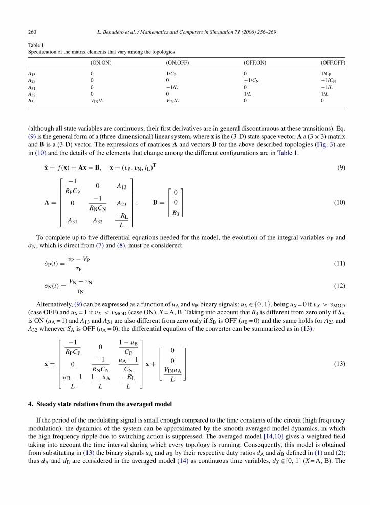
Table 1Specification of the matrix elements that vary among the topologies
(ON,ON) (ON,OFF) (OFF,ON) (OFF,OFF)
A13 0 1/CP 0 1/CP
A23 0 0 −1/CN −1/CN
A31 0 −1/L 0 −1/LA32 0 0 1/L 1/LB3 VIN/L VIN/L 0 0
(although all state variables are continuous, their first derivatives are in general discontinuous at these transitions). Eq.(9) is the general form of a (three-dimensional) linear system, where x is the (3-D) state space vector, A a (3 × 3) matrixand B is a (3-D) vector. The expressions of matrices A and vectors B for the above-described topologies (Fig. 3) arein (10) and the details of the elements that change among the different configurations are in Table 1.
x = f (x) = Ax + B, x = (vP, vN, iL)T (9)
A =
⎡⎢⎢⎢⎢⎢⎢⎣
−1
RPCP0 A13
0−1
RNCNA23
A31 A32−RL
L
⎤⎥⎥⎥⎥⎥⎥⎦
, B =
⎡⎢⎣
0
0
B3
⎤⎥⎦ (10)
To complete up to five differential equations needed for the model, the evolution of the integral variables σP andσN, which is direct from (7) and (8), must be considered:
σP(t) = vP − VP
τP(11)
σN(t) = VN − vN
τN(12)
Alternatively, (9) can be expressed as a function of uA and uB binary signals: uX ∈ {0, 1}, being uX = 0 if vX > vMOD(case OFF) and uX = 1 if vX < vMOD (case ON), X = A, B. Taking into account that B3 is different from zero only if SAis ON (uA = 1) and A13 and A31 are also different from zero only if SB is OFF (uB = 0) and the same holds for A23 andA32 whenever SA is OFF (uA = 0), the differential equation of the converter can be summarized as in (13):
x =
⎡⎢⎢⎢⎢⎢⎢⎣
−1
RPCP0
1 − uB
CP
0−1
RNCN
uA − 1
CNuB − 1
L
1 − uA
L
−RL
L
⎤⎥⎥⎥⎥⎥⎥⎦
x +
⎡⎢⎢⎣
0
0VINuA
L
⎤⎥⎥⎦ (13)
4. Steady state relations from the averaged model
If the period of the modulating signal is small enough compared to the time constants of the circuit (high frequencymodulation), the dynamics of the system can be approximated by the smooth averaged model dynamics, in whichthe high frequency ripple due to switching action is suppressed. The averaged model [14,10] gives a weighted fieldtaking into account the time interval during which every topology is running. Consequently, this model is obtainedfrom substituting in (13) the binary signals uA and uB by their respective duty ratios dA and dB defined in (1) and (2);thus dA and dB are considered in the averaged model (14) as continuous time variables, dX ∈ [0, 1] (X = A, B). The
L. Benadero et al. / Mathematics and Computers in Simulation 71 (2006) 256–269 261
same result (14) is given in [9] by using the time averaged equivalent circuit model [20]:
x =
⎡⎢⎢⎢⎢⎢⎢⎣
−1
RPCP0
1 − dB
CP
0−1
RNCN
dA − 1
CNdB − 1
L
1 − dA
L
−RL
L
⎤⎥⎥⎥⎥⎥⎥⎦
x +
⎡⎢⎢⎣
0
0VINdA
L
⎤⎥⎥⎦ (14)
The equilibrium point, which is the steady state for the averaged model, is obtained by equaling the vector field(14) to zero (see (15)). For an open loop control, the pair of coordinates (dA, dB) can freely be chosen in the range [0,1]. Consequently, the set of all possible steady state vectors x will lay on a surface inside the three-dimensional statespace. From the second and first equations in (15), it can be derived the steady state relations for both duty ratios (16)and (17), where iN and iP are the respective current loads (Fig. 2). Moreover, from these last expressions, an explicitexpression of the inductor current in front of both capacitor voltages can be obtained (18); although in this last equationboth positive and negative signs are possible, only the negative sign corresponds to a practical design, because thepositive case implies high inductor losses. Notice that if either vP = 0 (so dB = 1) or vN = 0 (so dA = 1), the circuit willdegenerate in either the buck-boost or the boost converter, respectively. Indeed, if RL were neglected, (18) would tendto the well known parabolic approximations for those elementary dc–dc converters:⎡
⎢⎢⎢⎢⎢⎢⎣
−1
RPCP0
1 − dB
CP
0−1
RNCN
dA − 1
CNdB − 1
L
1 − dA
L
−RL
L
⎤⎥⎥⎥⎥⎥⎥⎦
⎡⎢⎣
vP
vN
iL
⎤⎥⎦+
⎡⎢⎢⎣
0
0VINdA
L
⎤⎥⎥⎦ =
⎡⎢⎣
0
0
0
⎤⎥⎦ (15)
dA = 1 + vN
RNiL= 1 + iN
iL(16)
dB = 1 − vP
RPiL= 1 − iP
iL(17)
iL(vP, vN) = VIN
2RL∓√√√√( VIN
2RL
)2
− 1
RL
(v2
P
RP+ v2
N
RN− VINvN
RN
)(18)
Expression (18) can also be obtained from the energy conservation law, taking into account the averaged supply ofenergy that is dissipated in the resistances of the circuit:
VINdAiL = RLi2L + v2P
RP+ v2
N
RN
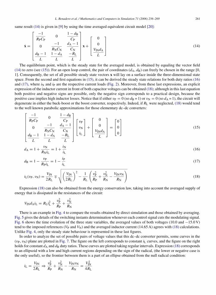
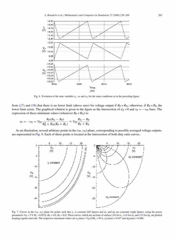
There is an example in Fig. 4 to compare the results obtained by direct simulation and those obtained by averaging.Fig. 5 gives the details of the switching instants determination whenever each control signal cuts the modulating signal.Fig. 6 shows the time evolution of the three state variables, the averaged values of both voltages (10.0 and −15.0 V)tend to the imposed references (VP and VN) and the averaged inductor current (14.65 A) agrees with (18) calculations.Unlike Fig. 4, only the steady state behaviour is represented in these last figures.
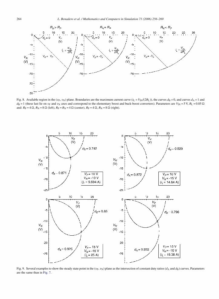
In order to analyze the set of possible pairs of voltage values that this dc–dc converter permits, some curves in the(vP, vN) plane are plotted in Fig. 7. The figure on the left corresponds to constant iL curves, and the figure on the rightholds for constant dA and dB duty ratios. These curves are plotted taking regular intervals. Expression (18) correspondsto an ellipsoid with a low and high current regions depending on the sign of the radical, (the lower or negative case isthe only useful), so the frontier between them is a part of an ellipse obtained from the null radical condition:
iL = VIN
2RL⇒ v2
P
RP+ v2
N
RN− VINvN
RN= V 2
IN
4RL
262 L. Benadero et al. / Mathematics and Computers in Simulation 71 (2006) 256–269
Fig. 4. Simulated dynamics using the switched model (up) and the averaged model (down). Parameters are: VIN = 5 V, L = 50 �H, RL = 0.05 �,RP = 4 �, RN = 8 �, CP = 200 �F, CN = 100 �F, rA = rB = 0.5 �, VP = 10 V, VN = −15 V, τP = τN = 40 �s, gPA = gNB = 0.05, gNA = gPB = 0, VU = 1 V,VL = 0 V, VRA = VRB = −5 V, gFA = gFB = 1, vMOD as in (3) being fMOD = 1/T = 150 kHz. Initial conditions are zero for all the state variables.
Particularizing the above expression in the symmetric case, the maximum output voltage will be:
vP = −vN = VIN
2
⎛⎝√
RPRN
RL(RP + RN)+(
RP
RP + RN
)2
− RP
RP + RN
⎞⎠
Together with these maximum values, which are reflected in the external curves given in Fig. 8, minimum values forvoltage outputs can also be higher than zero. This is due to the limit condition dB = 0, for which corresponding curve isalso plotted in the same figure. Three cases are represented for balanced and unbalanced loads; notice the enhancementof the unavailable region when RP < RN. In the particular symmetric voltage case (vP = −vN) it is straightforward
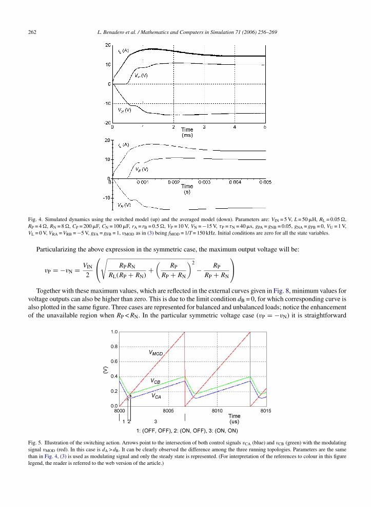
Fig. 5. Illustration of the switching action. Arrows point to the intersection of both control signals vCA (blue) and vCB (green) with the modulatingsignal vMOD (red). In this case is dA > dB. It can be clearly observed the difference among the three running topologies. Parameters are the samethan in Fig. 4, (3) is used as modulating signal and only the steady state is represented. (For interpretation of the references to colour in this figurelegend, the reader is referred to the web version of the article.)
L. Benadero et al. / Mathematics and Computers in Simulation 71 (2006) 256–269 263
Fig. 6. Evolution of the state variables iL, vP and vN for the same conditions as in the preceding figure.
from (17) and (18) that there is no lower limit (above zero) for voltage output if RP > RN; otherwise, if RP < RN thelower limit exists. The graphical solution is given in the figure as the intersection of dA = 0 and vP = −vN lines. Theexpression of these minimum values (whenever RP < RN) is:
vP = −vN = VINRP(RN − RP)
R2P + RN(RP + RL)
≈ VINRN − RP
RP + RN
As an illustration, several arbitrary points in the (vP, vN) plane, corresponding to possible averaged voltage outputs,are represented in Fig. 9. Each of these points is located at the intersection of both duty ratio curves.
Fig. 7. Curves in the (vP, vN) plane for points such that iL is constant (left figure) and dA and dB are constants (right figure), using the powerparameters VIN = 5 V, RL = 0.05 �, RP = 4 �, RN = 8 �. These curves, which are sections of surface (16) for iL, (14) for dA and (15) for dB, are plottedkeeping regular intervals. The respective maximum values are iL(max) = VIN/2/RL = 50 A, dA(max) = 0.927 and dB(max) = 0.888.
264 L. Benadero et al. / Mathematics and Computers in Simulation 71 (2006) 256–269
Fig. 8. Available region in the (vP, vN) plane. Boundaries are the maximum current curve (iL = VIN/(2RL)), the curves dB = 0, and curves dA = 1 anddB = 1 (these last lie on vP and vN axes and correspond to the elementary boost and buck-boost converters). Parameters are VIN = 5 V, RL = 0.05 �
and: RP = 4 �, RN = 8 � (left), RP = RN = 4 � (center), RP = 4 �, RN = 8 � (right).
Fig. 9. Several examples to show the steady state point in the (vP, vN) plane as the intersection of constant duty ratios (dA and dB) curves. Parametersare the same than in Fig. 7.
L. Benadero et al. / Mathematics and Computers in Simulation 71 (2006) 256–269 265
Unlike the switched model, the averaged model equations are smooth (unless there is saturation). Due to the controland the PWM voltage to time conversion according to VU and VL limits, expressions (19) and (20) are obtained. Allvariables in (14) and, (19) and (20) are the averaged values of the state variables previously defined. Because the explicitdependence of time has been suppressed, the averaged model is a five-dimensional autonomous system. However, itshould be noticed that the averaged model is no longer valid beyond the control limits or in the saturation region. Inthis case, dX is forced to be 0 or 1, so some topology will remain active during all the switching period. Border collisionbifurcations take place when parameters are varied until reaching some of these limit conditions [3,22,20,1,15,19].
dA = VU − VRA − gFAVIN − giAiL − gPA(vP − VP + σP) − gNA(VN − vN + σN)
VU − VL(19)
dB = VU − VRB − gFBVIN − giiL − gNB(VN − vN + σN) − gPB(vP − VP + σP)
VU − VL(20)
The goal of control is to govern both switches in order to maintain the desired outputs by adapting the respectiveduty ratios to possible disturbances in the source and loads. Any solution, as for instance the closed loops in Fig. 2 forPI control, should generate a stable dynamics. This condition will be treated in the following section.
5. Stability analysis
The set of five first order differential Eq. (14) plus (11) and (12), together with expressions (19) and (20) for thePWM duty ratios, define the five-dimensional and autonomous averaged system. The vector of state variables includingthe integrative terms is y = (vP, vN, iL, σP, σN). Expressions (16)–(18) for the correspondence of the inductor currentiL and the duty ratio pair (dA, dB) with the desired voltage pair (vP, vN) has been obtained only from (14). The restof equations defining the system must be contemplated in the frame of the complete system, so including the closedloops for control. First of all, the pair of simple conditions vP = VP and vN = VN, are the equilibrium solutions of (11)and (12), thus achieving a null error due to the integral action (Fig. 6). However, the stability of the system around thesteady state solution is a necessary condition to validate that result. The dynamics around the equilibrium points of adynamical system is well known to be equivalent to the linearized system in these points [8,10]. Thus, the stability ofour system will be investigated from the properties of the Jacobian matrix calculated in the equilibrium points:⎡
⎢⎢⎢⎢⎢⎢⎢⎢⎢⎢⎢⎢⎢⎢⎢⎣
gPBIL
VU − VL
1
CP
gNBIL
VU − VL
1
CP
3 × 3
submatrix below
−gPAIL
VU − VL
1
CN
−gNAIL
VU − VL
1
CN
−(
gPBVP + gPAV ′
VU − VL
)1
L−(
gNBVP + gNAV ′
VU − VL
)1
L
1
τP0 0 0 0
0−1
τP0 0 0
⎤⎥⎥⎥⎥⎥⎥⎥⎥⎥⎥⎥⎥⎥⎥⎥⎦
⎡⎢⎢⎢⎢⎢⎢⎢⎣
(− 1
RP+ gPBIL
VU − VL
)1
CP
−gNBIL
VU − VL
1
CP
(D′
B + rBIL
VU − VL
)1
CP
−gPAIL
VU − VL
1
CN
(− 1
RN+ gNAIL
VU − VL
)1
CN−(
D′A + rAIL
VU − VL
)1
CN
−(
D′B + gPBVP + gPAV ′
VU − VL
)1
L
(D′
A + gNBVP + gNAV ′
VU − VL
)1
L−(
RL + rBVP + rAV ′
VU − VL
)1
L
⎤⎥⎥⎥⎥⎥⎥⎥⎦
Above, there is an explicit expression of the Jacobian J in the given equilibrium point defined for VP and VN, andbeing dA, dB and IL the duty ratios and the inductor current that can be obtained from (16)–(18). The values for theintegrative terms σP and σN in the steady state conditions do not appear explicitly in the Jacobian, but they are availablefrom (19) and (20). The generic Jij element of the Jacobian is obtained as the first derivative of the i field equation
266 L. Benadero et al. / Mathematics and Computers in Simulation 71 (2006) 256–269
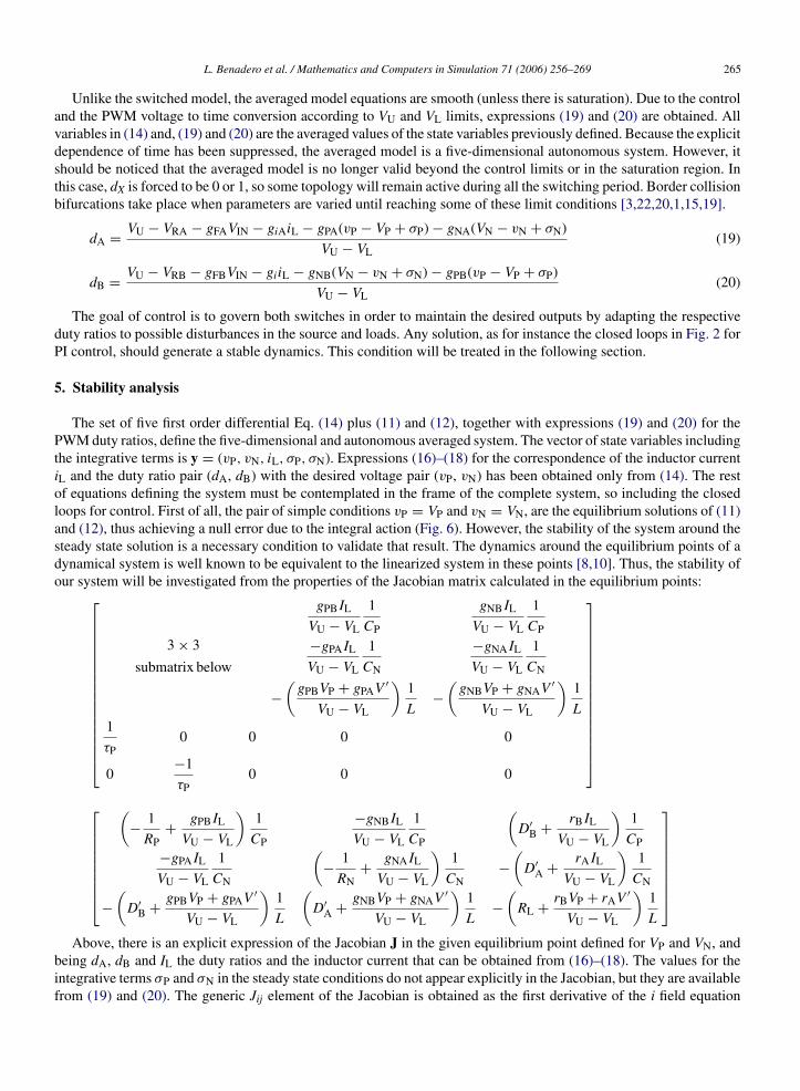
Fig. 10. Representation of the higher real part of the Jacobian eigenvalues Re(λ) (s−1). Parameters are the same as in Fig. 4 apart from specificparameter or parameters that are varied in each diagram.
respect to the j element of the state vector y. The 3 × 3 submatrix is printed separately, VIN − VN is abbreviated as V′,1 − dA as D′
A and 1 − dB as D′B.
To prove stability, several diagrams are plotted in Fig. 10. The asymptotic local stability condition implies that allthe real parts of the Jacobian eigenvalues, Re(λ), must be negative. Moreover, the closer are Re(λ) to zero, the longer are
L. Benadero et al. / Mathematics and Computers in Simulation 71 (2006) 256–269 267
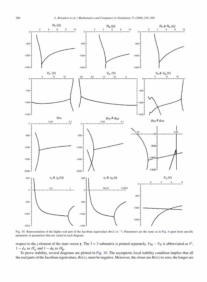
Fig. 11. Saddle-node bifurcation corresponding to the limit of VP parameter (being iL = VIN/(2RL)). Unlike in Fig. 10, the positive real eigenvalueof the unstable (higher inductor current) solution is also included.
the transients. The higher values of Re(λ) are therefore more significant in the behaviour of the system from the pointof view of transient and stability, and consequently, only these are represented in the diagrams. As the eigenvalues canbe either real or complex conjugate, the line representing a given eigenvalue will split into two lines whenever there isa transition between complex conjugates and real cases. The same parameter set than in Fig. 4 has been chosen, apartfrom the specific parameter that is varied in each diagram to look for the stability margin (negative results). In somediagrams, two parameters are varied simultaneously as it is indicated in the parameter axis. An inspection of thesediagrams shows that eigenvalues are negative around the chosen parameter set. From top to bottom and from left toright, the diagrams are made by varying the source voltage, the load resistors and the following control parameters:voltage references for calculating the error signals, gains for both PI blocks, current inductor gains, time constant ofPI blocks and the amplitude of the modulating signal.
Two kinds of bifurcations are observed in these diagrams. The so called tangent or saddle-node bifurcation corre-sponds to turning points because there are no longer equilibrium points beyond the critical point, while two solutions,one stable and the other unstable, coexist before that point. Moreover, in this critical turning point, the pair of solutionsjoins in such a manner that two eigenvalues, one for the stable and other for the unstable case, are real and tend tozero at the turning point from the negative and positive side, respectively. This behaviour is given on one side of thesix diagrams on the top, being only the stable case represented. Although it is not convenient to approach that pointin a practical design, the set of both the stable and the unstable solutions (lower and higher inductor current in (18))is represented separately in Fig. 11 to illustrate the explained behaviour. As it could be expected, this bifurcationcorresponds to the steady state limits that have been detailed in the previous section. The other kind of bifurcation,which is observed in some of the rest of diagrams, corresponds to a complex eigenvalue crossing the abscise axis. Thiscondition holds for a Hopf bifurcation, so long (stable or unstable) transients will be present around that point. Fig. 12
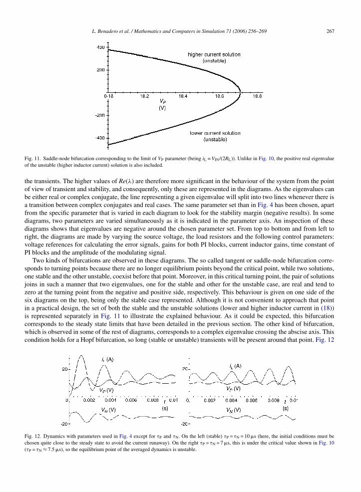
Fig. 12. Dynamics with parameters used in Fig. 4 except for τP and τN. On the left (stable) τP = τN = 10 �s (here, the initial conditions must bechosen quite close to the steady state to avoid the current runaway). On the right τP = τN = 7 �s, this is under the critical value shown in Fig. 10(τP = τN ≈ 7.5 �s), so the equilibrium point of the averaged dynamics is unstable.

268 L. Benadero et al. / Mathematics and Computers in Simulation 71 (2006) 256–269
shows two examples in both sides of bifurcation with the time constants of the PI block; it is clearly observed the longstable and unstable transients due to the proximity of bifurcation; the initial conditions have been chosen to observethis behaviour, because around the bifurcation, the dynamics tends to some blocking topology favoured by the integralaction. Whenever the power parameter set or even the output references are modified, the control parameters shouldbe adapted to optimize the new design.
Relating to the PI blocks connection, the control requires a somewhat crossed feedback. From the results shown inFig. 10, a reasonable design requires gains gNA and gPB near zero, while gPA and gNB must be positive. Consequently tothis, the error signal for the positive load drives switch SA and the error signal for the negative load drives SB. Lookingat (16) and (17), duty ratios dA and dB influence the negative and the positive load, respectively. The reciprocity in therelations between the inductor current and both duty ratios (these variables intervene in the flow of current (14) andthe inductor current does in both duty ratios expressions (16) and (17)) can be a qualitative explanation of this fact.
Finally, it has to be pointed out in the following remarks. Firstly, the averaged model is an approximation basedon high frequency switching so as to give minimum variations of variables during a cycle. With the parameter setused here, it is observed in Fig. 5 a non-negligible ripple in the inductor current; although this fact will produce ashift in the results in the steady state and transients, the dynamics plotted in Fig. 4 using the averaged model anddirect simulations are enough similar. Another question refers to the possibility of sliding, this situation will be doneif after a given state transition, the field in the subsequent state points towards the preceding state or in other words,if after switching the control signal has an absolute slope (in a temporal representation) higher than the modulatingsignal. To avoid the resulting uncontrolled switching, a RS flip–flop, placed between the comparator and the driver, iscommonly used. Whenever the flip–flop works, the averaged model continues giving a roughly approximation for thesteady state. However, although this continuous time averaged model can explain Hopf and saddle-node bifurcations,there is the need for a discrete time model (commonly based on Poincare approach) [8,5] to deal with flip bifurcationthat is prompted to appear in this case. The last indication is the fact that PI controllers in these devices favour thepossibility for the dynamics to undergo an undesired situation. This is due to the coexistence of the nominal dynamicswith blocking states. To prevent from this, the initial conditions when the integral action is started should be inside thebasin of attraction belonging to the proper steady state.
6. Conclusions
A novel single inductor two inputs-two outputs switching dc–dc converter has been analysed. There is no need inthis device for symmetry in its positive and negative outputs. A PWM control including two PI blocks, whose inputs areeach of the error signals, has been proved to provide a stable behaviour. The frame of averaging has been used to makemore comprehensive the analysis. Extensive details of the steady state properties are given from the model. An explicitexpression for the Jacobian has also been derived and used to prove stability and the influence of some representativeparameters. The present analysis is not complete due to limitations of averaging, so more research is needed to completethe task, mainly about the stability criteria under lower switching frequencies. Also, some experimental arrangementswill be made to look for the valid range of the results foreseen in the analysis and to explore the effect of auxiliarycircuitry for instance to keep duty cycle inside a given range or antiwindup to limit the integral term.
Acknowledgment
This work was supported by the Spanish ‘Ministerio de Educacion y Ciencia’ under Grants ENE2005-06934/ALTand TEC-2004-05608-C02-02.
References
[1] S. Banerjee, E. Ott, J.A. Yorke, G.H. Yuan, Anomalous bifurcations in dc–dc converters: borderline collisions in piecewise smooth maps, in:Proceedings of the 28th IEEE PESC, vol. 2, 1997, pp. 1337–1344.
[2] R.M. Bass, P.T. Krein, Limit cycle geometry and control in power electronic systems, in: Proceedings of the 32nd Midwest Symposium onCircuits and Systems, 1989, pp. 785–787.
[3] M. di Bernardo, C.J. Budd, A.R. Champneys, Grazing, skipping and sliding: analysis of the non-smooth dynamics of the dc/dc buck converter,Nonlinearity 11 (4) (1998) 859–890.

L. Benadero et al. / Mathematics and Computers in Simulation 71 (2006) 256–269 269
[4] M. di Bernardo, M.I. Feigin, S.J. Hogan, M.E. Homer, Local analysis of C-bifurcations in N-dimensional piecewise-smooth dynamical systems,Chaos Solutions Fractals 10 (11) (1999) 1881–1908.
[5] M. di Bernardo, F. Vasca, Discrete-time maps for the analysis of bifurcations and chaos in dc/dc converters, IEEE Trans. Circuits Syst. I 47 (2)(2000) 130–143.
[6] J.H.B. Deane, D.C. Hamill, Instability, subharmonics and chaos in power electronic systems, IEEE Trans. Power Electron. 5 (3) (1990) 260–268.[7] I. Denes, I. Nagy, Two models for the dynamic behaviour of a dual-channel buck and boost dc–dc converter, Electromotion 10 (4) (2003)
556–561.[8] O. Dranga, B. Buti, I. Nagy, Stability analysis of a feedback-controlled resonant DC–DC converter, IEEE Trans. Ind. Electron. 50 (1) (2003)
141–152.[9] R. Giral, J. Calvente, R. Leyva, A. El Aroudi, G. Arsov, L. Martinez-Salamero, Symmetrical power supply for 42 V automotive applications,
AAS (2003) (Macedonia).[10] J. Guckenheimer, P. Holmes, Nonlinear Oscillations, Dynamical Systems and Bifurcations of Vector Fields, Springer-Verlag, 1983.[11] J. Hamar, I. Nagy, Control features of dual-channel DC–DC converters, IEEE Trans. Ind. Electron. 49 (6) (2002) 1293–1305.[12] J. Hamar, I. Nagy, Asymmetrical operation of dual channel resonant DC–DC converters, IEEE Trans. Power Electron. 18 (1) (2003) 83–94.[13] J.G. Kassakian, M. Schlecht, G.C. Verghese, Principles of Power Electronics, Addison-Wesley, 1991.[14] P.T. Krein, Elements of Power Electronics, Oxford University Press, 1998.[15] P.T. Krein, R.M. Bass, Types of instability encountered in simple power electronics circuits: unboundedness, chattering and chaos, IEEE APEC
(1990) 191–194.[16] Y.A. Kutnetsov, Elements of Applied Bifurcation Theory, Springer-Verlag, 1998.[17] N. Mohan, T.M. Undeland, W.P. Robins, Power Electronics: Converters, Applications and Design, John Wiley & Sons, 2003.[18] I. Nagy, O. Dranga, Bifurcation in a dual channel resonant dc–dc converter, IEEE Int. Symp. Ind. Electron. ISIE (2000) 495–500.[19] B. Robert, C. Robert, Border collision bifurcations in a chaotic PWM H-bridge single-phase inverter, in: Proceedings of the 10th International
Power Electronics and Motion Control Conference (EPE-PEMC’ 02), 2002.[20] C.K. Tse, Complex Behaviour of Switching Power Converters, CRC Press, 2004.[21] C.K. Tse, M. di Bernardo, Complex behavior in switching power converters, Proc. IEEE 90 (5) (2002) 768–781.[22] Z.T. Zhusubaliyev, E. Mosekilde, Bifurcation and chaos in piecewise-smooth systems, World Scientific (2003).
Related Documents