Baseband Transmitter Training System ST2134 Operating Manual Ver 1.1 An ISO 9001 : 2000 company 94-101, Electronic Complex Pardeshipura, Indore- 452010, India Tel : 91-731- 2570301/02, 4211100 Fax: 91- 731- 2555643 email : [email protected] Website : www.scientech.bz Toll free : 1800-103-5050

Welcome message from author
This document is posted to help you gain knowledge. Please leave a comment to let me know what you think about it! Share it to your friends and learn new things together.
Transcript

8/14/2019 ST2134 trainer kit manual
http://slidepdf.com/reader/full/st2134-trainer-kit-manual 1/171
Baseband Transmitter
Training System
ST2134
Operating ManualVer 1.1
An ISO 9001 : 2000 company
94-101, Electronic Complex Pardeshipura,Indore- 452010, India
Tel : 91-731- 2570301/02, 4211100Fax: 91- 731- 2555643
email : [email protected] Website : www.scientech.bz
Toll free : 1800-103-5050

8/14/2019 ST2134 trainer kit manual
http://slidepdf.com/reader/full/st2134-trainer-kit-manual 2/171
ST2134
Scientech Technologies Pvt. Ltd. 2

8/14/2019 ST2134 trainer kit manual
http://slidepdf.com/reader/full/st2134-trainer-kit-manual 3/171
ST2134
Scientech Technologies Pvt. Ltd. 3
Baseband Transmitter Training System
ST2134
Table of Contents
1. Introduction 6
2. Features 7
3. Technical Specifications 8
4. Software installation 8
5. Software window Control details 9
6. Introduction to Baseband Communication 10
7. Experiments
• Experiment 1 12
Study, Analysis and Measurement of Variable Clock and Variable
Pattern Generator
• Experiment 2 18
Study, Analysis and Measurement of 1Bit Encoding with Variable
Clock and Variable Pattern
• Experiment 3 21
Study, Analysis and Measurement of ASK Modulation with 1Bit
Encoding
• Experiment 4 25Study, Analysis and Measurement of BPSK Modulation with 1Bit
Encoding
• Experiment 4A 29Study, Analysis and Measurement of DPSK Modulation with
1-Bit Encoding
• Experiment 5 32
Study and Analysis of BPSK Constellation
• Experiment 6 35
Study, Analysis and Measurement of FSK Modulation with 1BitEncoding
• Experiment 7 39Study, Analysis and Measurement of two bit encoding with pattern
generator and clock.
• Experiment 8 43
Study, Analysis and Measurement of QPSK Modulation with 2 Bit
Encoding
• Experiment 9 48
Study, Analysis and Measurement of QPSK Constellation

8/14/2019 ST2134 trainer kit manual
http://slidepdf.com/reader/full/st2134-trainer-kit-manual 4/171
ST2134
Scientech Technologies Pvt. Ltd. 4
• Experiment 10 51
Study, Analysis and Measurement of Rate 1/2 Convolutional Encoding
• Experiment 11 58
Study, Analysis and Measurement of QPSK Modulation withrate 1/2 Bit Encoding
• Experiment 12 63
Study, Analysis and Measurement of OQPSK Modulationwith 2 Bit Encoding
• Experiment 13 70
Study, Analysis and Measurement of OQPSK Constellation
• Experiment 14 73Study, Analysis and Measurement of OQPSK Modulation with
rate 1/2 Bit Encoding
• Experiment 15 78Study, Analysis and Measurement of π/4 QPSK Modulation
with 2 Bit Encoding
• Experiment 16 86
Study, of π/4 QPSK Constellation and eye pattern
• Experiment 17 89
Study, Analysis and Measurement of π/4 QPSK Modulation with
rate 1/2 Bit Encoding
• Experiment 18 97
Study, Analysis and Measurement of three bit encoding with pattern
generator and clock.
• Experiment 19 101
Study, Analysis and Measurement of 8-PSK modulation with
three bit encoding, pattern generator and clock
• Experiment 20 105
Study of 8 PSK Constellation and eye pattern
• Experiment 21 108
Study, Analysis and Measurement of rate 2/3 convolutional encoding
• Experiment 22 116
Study, Analysis and Measurement of 8-PSK modulation with
rate 2/3 convolution encoding, pattern generator and clock
• Experiment 23 124Study, Analysis and Measurement of four bit encoding with pattern
generator and clock

8/14/2019 ST2134 trainer kit manual
http://slidepdf.com/reader/full/st2134-trainer-kit-manual 5/171
ST2134
Scientech Technologies Pvt. Ltd. 5
RoHS Compliance
Scientech Products are RoHS Complied.
RoHS Directive concerns with the restrictive use of Hazardous substances (Pb,
Cd, Cr, Hg, Br compounds) in electric and electronic equipments.
Scientech products are “Lead Free” and “Environment Friendly”.
It is mandatory that service engineers use lead free solder wire and use the
soldering irons upto (25 W) that reach a temperature of 450°C at the tip as the
melting temperature of the unleaded solder is higher than the leaded solder.
• Experiment 24 128
Study, Analysis and Measurement of 16-PSK modulation withfour bit encoding, pattern generator and clock.
• Experiment 25 133Study and Analysis of 16-PSK constellation
• Experiment 26 136
Study, Analysis and Measurement of rate 3/4 rate convolution encoding
• Experiment 27 144Study, Analysis and Measurement of 16 PSK modulation with
rate 3/4 convolution encoding
• Experiment 28 152Study, Analysis, and measurement of 16 QAM Modulation with
four bit encoding.
• Experiment 29 158Study and analysis of 16QAM Constellation
• Experiment 30 161
Study, Analysis and Measurement of 16 QAM modulation with rate3/4 convolution encoding
8. FAQ’s 169
9. Warranty 170
10. List of Accessories 170

8/14/2019 ST2134 trainer kit manual
http://slidepdf.com/reader/full/st2134-trainer-kit-manual 6/171
ST2134
Scientech Technologies Pvt. Ltd. 6
Introduction
Today advanced communication technologies are growing in a tremendous way.
Technologies like wireless communication, mobile communication, satellite
communication, data communication, RF ID etc enters in our daily lives.In most fundamental sense, Baseband communication plays a very important role in
above communication technologies and is the basic need for any transmission,
communication System Elements.
Considering this demand Scientech has introduced Baseband Transmitter Training
System in the filed of education. This training system is an ideal solution to bridge the
gap between theoretical studies and practical results.
Using this training system student can be able to understand systematic journey ofcommunication transmitter system. All major blocks required in a baseband
transmitter blocks are covered and test points are provided for every step.

8/14/2019 ST2134 trainer kit manual
http://slidepdf.com/reader/full/st2134-trainer-kit-manual 7/171
ST2134
Scientech Technologies Pvt. Ltd. 7
Features
• Baseband Transmitter Training System is based on advanced technology
• Encoding (1 bit, 2 bit, 3bit, 4 bits, convolutional 1/2, 2/3, 3/4 encoding etc
• Modulation techniques ( ASK, PSK, DPSK, FSK, QPSK, OQPSK, π/4,
QPSK, 8-PSK, 16-PSK, 16-QAM )
• Constellation (Vector) Pattern for respective modulation
• Eye Pattern view
• Training System can be controlled in hardware mode or in software modewithout need of an external Data Acquisition Card
• Training System has more than 60 test points, which will help students to
observe the signal on Analog Oscilloscope, DSO & Logic Analyzer
• With the help of Real-time Software student can control as well as
Analyze digital signal, Analog signal, and Mixed Signal and XY mode
• Simulations for different Encoding and Modulation Techniques are also
provided within ST2134 Software CD
Technical Specifications• On board digitally Synthesized Sine and Cosine, wave Generator with
Variable step frequency.
• On board Clock Generator with Step Variable Frequencies (75Hz, 150Hz,
300Hz, 600Hz, 1200Hz, 2400Hz, 4800Hz & 9600 KHz).
• On board Data generator with Step Variable data length (4, 8, 16, 32, 64 bit)
and variable data type select (i.e. 64 combinations are possible).
• Encoding (1 bit, 2 bit, 3bit, 4 bits, convolutional 1/2, 2/3 , 3/4 encoding etc.
• Modulation techniques (ASK, PSK, DPSK, FSK, QPSK, OQPSK, π/4 QPSK,
8-PSK, 16-PSK, 16-QAM )
• Power supply: 220 V + 10% 50 Hz / 60 Hz
• Power Consumption: 2.5VA (approx.)
• Weight: 1.5 Kg (approx.)
• Dimension(mm): W365 X D260 X H175ST2134

8/14/2019 ST2134 trainer kit manual
http://slidepdf.com/reader/full/st2134-trainer-kit-manual 8/171
ST2134
Scientech Technologies Pvt. Ltd. 8
Software Installation Procedure
• System Requirement - OS – Windows XP / 2000 / service pack 2 - PORT –
Parallel port (Mode – Standard port type SPT)
• Install ST2134 Software from the CD provided with Baseband TransmitterTraining system.
• To Open software go to > Start > BTTS software.
• Select Simulation / Real time software option.
• For Real time software connect ST2134 trainer to Parallel port of yourComputer.
Software window Control details
Range selection for experiments from 1 – 16 & 17 – 30 can be done through
“Experiment Range Select” DIP provided on ST2134.
8/14/2019 ST2134 trainer kit manual
http://slidepdf.com/reader/full/st2134-trainer-kit-manual 9/171
ST2134
Scientech Technologies Pvt. Ltd. 9
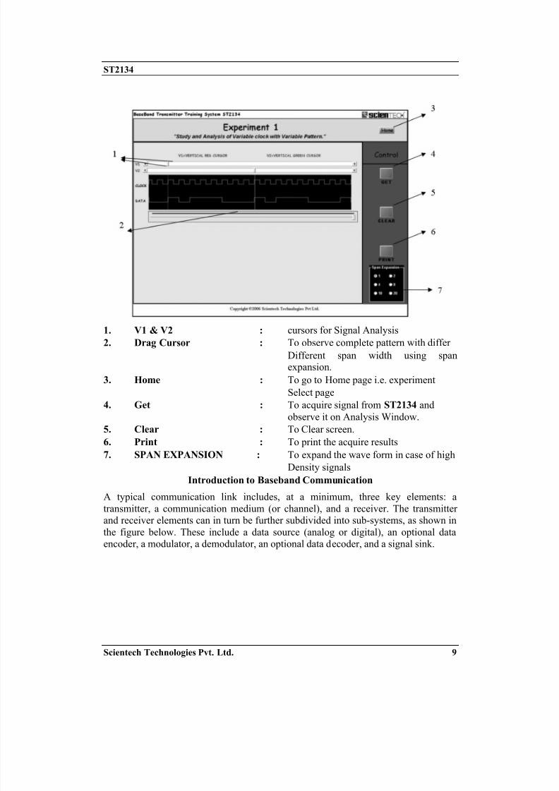
1. V1 & V2 : cursors for Signal Analysis
2. Drag Cursor : To observe complete pattern with differ
Different span width using spanexpansion.
3. Home : To go to Home page i.e. experiment
Select page
4. Get : To acquire signal from ST2134 and
observe it on Analysis Window.5. Clear : To Clear screen.
6. Print : To print the acquire results
7. SPAN EXPANSION : To expand the wave form in case of high
Density signals
Introduction to Baseband Communication
A typical communication link includes, at a minimum, three key elements: a
transmitter, a communication medium (or channel), and a receiver. The transmitter
and receiver elements can in turn be further subdivided into sub-systems, as shown in
the figure below. These include a data source (analog or digital), an optional data
encoder, a modulator, a demodulator, an optional data decoder, and a signal sink.

8/14/2019 ST2134 trainer kit manual
http://slidepdf.com/reader/full/st2134-trainer-kit-manual 10/171
ST2134
Scientech Technologies Pvt. Ltd. 10
Key Communication Sub-Systems
All communication systems include some sort of data source , which generates the
information signal that is intended to be sent to a particular receiver. This signal can
be either an analog signal such as speech, or a digital signal such as a binary data
sequence. This signal is typically a baseband signal represented by a voltage level.For analog signals, it is often desirable to represent the signal digitally by undergoinga quantization process prior to transmission. This step converts the analog signal into
a digital signal. While some information is lost in this process, the resulting digitalsignal is often far less susceptible to the effects of noise in the transmission channel.
An encoder can be used to add redundancy to a digital data stream, in the form of
additional data bits, in a way that provides an error correction capability at the
receiver. This overall process is referred to as Forward Error Correction (FEC).Among the most popular FEC schemes are convolutional coding, block coding and
trellis coding. It is important to note that usually the output bit rate of an encoder isnot equal to the input bit rate. To properly distinguish between the two bit rates, the
transmitter’s input rate is referred to as the information data rate, while thetransmitter output rate is referred to as the channel data rate.
Depending on the type of information signal and the particular transmission medium,
different modulation techniques are employed. Modulation refers to the specific
technique used to represent the information signal as it is physically transmitted to the
receiver. For example, in Amplitude Modulation (AM), the information is represented
by amplitude variations of the carrier signal.
Once the signal is modulated, it is sent through a transmission medium, also known as
a channel , to reach the intended receiver. This may be a copper wire, coax cable, or
the atmosphere in the case of a radio transmission. To some extent, all channels
introduce some form of distortion to the original signal. Many different channel
models have been developed to mathematically represent such distortions. Acommonly used channel model is the Additive White Gaussian Noise (AWGN)
channel. In this channel, noise with uniform power spectral density (hence the term
white) is assumed to be added to the information signal. Other types of channels
include fading channels and multipath channels.

8/14/2019 ST2134 trainer kit manual
http://slidepdf.com/reader/full/st2134-trainer-kit-manual 11/171
ST2134
Scientech Technologies Pvt. Ltd. 11
When the transmitted signal reaches the intended receiver, it undergoes a
demodulation process. This step is the opposite of modulation and refers to the
process required to extract the original information signal from the modulated signal.
Demodulation also includes any steps associated with signal synchronization, such as
the use of phase-locked loops in achieving phase coherence between the incomingsignal and the receiver’s local oscillator.
When data encoding is included at the transmitter, a data decoding step must be
performed prior to recovering the original data signal. The signal decoding process is
usually more complicated than the encoding process and can be very computationally
intensive. Efficient decoding schemes, however, have been developed over the
years—one example is the Viterbi decoding algorithm, which is used to decode
convolutionally encoded data.
Finally, an estimate of the original signal is produced at the output of the receiver.The receiver’s output port is sometimes referred to as the signal sink . A key success
criteria for communications engineers is determining how well the source information
was recreated at the receiver. Several metrics are available to evaluate acommunication’s link performance, as for example the received Bit Error Rate (BER)
in the case of digital signals. Other valuable performance indicators include the
received signal to noise ratio, eye pattern diagrams and phase scatter plots to name a
few.
Baseband Communication

8/14/2019 ST2134 trainer kit manual
http://slidepdf.com/reader/full/st2134-trainer-kit-manual 12/171
ST2134
Scientech Technologies Pvt. Ltd. 12
Experiment 1
Objective :
Study, Analysis and Measurement of Variable Clock and Variable Pattern
GeneratorTheory :
Variable Clock Generator :
Clock Generator is the heart and is one of the important block in any digital sequentialcircuit design. In ST2134 digitally synthesized clock of 50 % duty cycle with multiply
of frequencies are generated.
Clock of standard frequencies (75Hz,150 Hz, 300, Hz, 600Hz, 1200Hz, 2400Hz,
4800Hz, 9600Hz) can be controlled using DIP switches D2, D3, D4 both in Hardware
and Software mode and can be observed on test point TP2.
Below Table shows, the position of DIP switches (D2, D3, D4) and respective output
clock frequency at test point tp.2.
Serial
Number
DIP Switches
D2 D3 D4
Clock frequency at TP
2 (Hz)
1 000 75
2 001 150
3 010 300
4 011 600
5 100 1200
6 101 2400
7 110 4800
8 111 9600
Variable Pattern Generator with Variable Type
Pattern Generator or Data generator is also a basic requirement for digital circuit
analysis.
Pattern or Data Generator is used in digital Communication as a data source.
In ST2134 Pattern Generator is provided with both variable length and variable type.
DIP switches D7 and D8 are used to change the Length or the repetition rate of the
pattern. Similarly, for a selected length of pattern its type may be varied usingDIPswitches D5 and D6.
Pattern of different type and different length can be selected using DIP switches (D5 –
D8) and can be observed on the Test Point TP 3.

8/14/2019 ST2134 trainer kit manual
http://slidepdf.com/reader/full/st2134-trainer-kit-manual 13/171
ST2134
Scientech Technologies Pvt. Ltd. 13
Below Table shows different possible combination
Serial
Number
DIP Switches
D7 D8 (Length)
DIP Switches
D5 D6 (Type)
Pattern Length - Type
1 00 00 64 Bits – Type1
2 00 01 64 Bits – Type2
3 00 10 64Bits – Type3
4 00 11 64 Bits – Type4
5 01 00 32 Bits – Type1
6 01 01 32 Bits – Type2
7 01 10 32 Bits – Type3
8 01 11 32 Bits – Type4
9 10 00 16 Bits – Type1
10 10 01 16 Bits – Type2
11 10 10 16 Bits – Type3
12 10 11 16 Bits – Type4
13 11 00 8 Bits – Type1
14 11 01 8 Bits – Type2
15 11 10 8 Bits – Type3
16 11 11 8 Bits – Type4
Figure below shows length and types of patterns :
Patterns of 8-Bit length :

8/14/2019 ST2134 trainer kit manual
http://slidepdf.com/reader/full/st2134-trainer-kit-manual 14/171
ST2134
Scientech Technologies Pvt. Ltd. 14
Patterns of 16-Bit length :
Patterns of 32-Bit length :
Patterns of 64-Bit length :
Procedure :
• Hardware Mode Steps
1. Switch ‘On’ Power Switch.
2. Observe and measure system clock at Test Point TP1.
3. For hardware mode Set DIP D1 to logic 0 (down position)
4. Set DIP D2, D3, D4 to 000.
5. Observe Clock frequency at test point TP2 with respect to Ground, it should
be 75Hz.
6. Set DIP D1, D2, D3, D4 to 0001, 0010, 0011, 0100, 0101, 0110, 0111 andobserve their respective frequencies at test point TP2.
7. Set pattern length by using DIP D7, D8 (00 – 64 bits, 01 – 32 bits, 10 – 16
bits, 11 – 8 bits) and observe corresponding bit pattern at Test Point TP3.
8. For above Pattern Length you can select pattern type using DIP D5, D6 (00 –Type 1, 01 – Type2, 10 – Type3, 11 – Type 4)
• Software Mode Steps
1. Switch ‘On’ Power Switch of ST2134.
2. For software mode Set DIP D1 to logic 1 (up position).
3. Open ST2134 software from start > ….
4. Use DIP D9 to select the set of Experiment i.e. experiment range to be
performed.
5. Click EXP1.

8/14/2019 ST2134 trainer kit manual
http://slidepdf.com/reader/full/st2134-trainer-kit-manual 15/171
ST2134
Scientech Technologies Pvt. Ltd. 15
6. Set DIP D2, D3, D4 from 000 to 111 and observe the corresponding
frequencies on software window.
7. Set pattern length by using DIP D7, D8 (00 – 64 bits, 01 – 32 bits, 10 – 16
bits, 11 – 8 bits) of ST2134 8. For above Pattern Length you can select pattern type using DIP D5, D6 (00 –
Type 1, 01 – Type2, 10 – Type3, 11 – Type 4)
Observation :
DSO Result for Reference
Software Result for Reference

8/14/2019 ST2134 trainer kit manual
http://slidepdf.com/reader/full/st2134-trainer-kit-manual 16/171
ST2134
Scientech Technologies Pvt. Ltd. 16
User Result : (in hardware mode)
Clock ….
PatternLength …..
Clock ….
Pattern
Length …..
Clock ….
Pattern
Length …..
Clock ……
PatternLength …..
Clock ….
PatternLength …..
Clock ….
Pattern
Length …..

8/14/2019 ST2134 trainer kit manual
http://slidepdf.com/reader/full/st2134-trainer-kit-manual 17/171
ST2134
Scientech Technologies Pvt. Ltd. 17
Clock
…….
PatternLength
…….
Clock…….
Pattern
Length
……
Result :

8/14/2019 ST2134 trainer kit manual
http://slidepdf.com/reader/full/st2134-trainer-kit-manual 18/171
ST2134
Scientech Technologies Pvt. Ltd. 18
Experiment 2
Objective :
Study, Analysis and Measurement of 1Bit Encoding with Variable Clock and
Variable PatternTheory :
Refer Experiment 1 Theory.
One bit encoded data is similar to the data output from data/pattern generator.Frequency of the data after encoding will remains the same as of clock generator.
Figure below shows the clock, Data from generator and One bit encoded data.
Procedure :
• Hardware Mode Steps
1. Switch ‘On’ Power Switch.
2. For hardware mode Set DIP D1 to logic 0 (down position).
3. Set DIP D2, D3, D4 to 000.
4. Observe Clock frequency at test point TP2 with respect to Ground, it should
be 75 Hz.5. Set output control i.e. DIP D12,D13,D14,D15, D16 to (00001)
6. Observe 1 bit encoded data at test point TP8 and compare it with data at TP3.
7. For clock frequency, Pattern length and pattern Type setting referExperiment 1.
• Software Mode Steps
1. Switch ‘On’ Power Switch of ST2134.
2. For software mode Set DIP D1 to logic 1 (up position).
3. Open ST2134 software from start > ….
4. Use DIP D9 to select the set of Experiment i.e. experiment range to be
performed.
5. Click EXP2.
6. Set DIP D2, D3, D4 from 000 to 111.

8/14/2019 ST2134 trainer kit manual
http://slidepdf.com/reader/full/st2134-trainer-kit-manual 19/171
ST2134
Scientech Technologies Pvt. Ltd. 19
7. Set pattern length by using DIP D7, D8 (00 – 64 bits, 01 – 32 bits, 10 – 16
bits, 11 – 8 bits) of ST2134
8. For above Pattern Length you can select pattern type using DIP D5, D6 (00 –
Type 1, 01 – Type2, 10 – Type3, 11 – Type 4)9. Click GET button and observe the corresponding clock signal, pattern and 1
bit encoded data on software window.
10. Use curser V1 and V2 for Analysis.
Observation :
DSO Result for Reference

8/14/2019 ST2134 trainer kit manual
http://slidepdf.com/reader/full/st2134-trainer-kit-manual 20/171
ST2134
Scientech Technologies Pvt. Ltd. 20
Software Result for Reference
User Result (Hardware Mode) :
Clock ….
Pattern Length1 bit encoding
Clock …..
Pattern Length
1 bit encoding
Clock …..
Pattern Length
1 bit encoding
Clock ……
Pattern Length
1 bit encoding
Result :

8/14/2019 ST2134 trainer kit manual
http://slidepdf.com/reader/full/st2134-trainer-kit-manual 21/171
ST2134
Scientech Technologies Pvt. Ltd. 21
Experiment 3
Objective :
Study, Analysis and Measurement of ASK Modulation with 1Bit Encoding.
Theory :
Modulation is a process of facilitating the transfer of information over a medium.
Sound transmission in air has limited range for the amount of power your lungs can
generate. To extend the range your voice can reach, we need to transmit it through a
medium other than such as a phone line or radio. The process of converting
information (voice / data) so that it can be successfully sent through a medium ( wire /
radio waves ) is called modulation.
We begin our discussion of digital modulation by starting with the ASK Modulationtechnique. Sinusoid wave has three different parameters that can be varied. These are
its amplitude, phase & frequency. Modulation is a process of mapping such that ittakes your data signal converts it into some aspect of a sine wave and then transmits
the sine wave, leaving the actual information behind.
In ASK Modulation, the amplitude of the carrier is changed in response to
information and all else is kept fixed. Bit 1 is transmitted by a carrier of one particularamplitude. To transmit 0, we change the amplitude keeping the frequency constant.
On-Off Keying (OOK) is a special form of ASK, where one of the amplitude is zeroas shown below.
Figure 1
Baseband information sequence – 011111101110110001 and Binary ASK (OOK)
Modulated Signal

8/14/2019 ST2134 trainer kit manual
http://slidepdf.com/reader/full/st2134-trainer-kit-manual 22/171
ST2134
Scientech Technologies Pvt. Ltd. 22
Procedure :
• Hardware Mode Steps
1. Switch ‘On’ Power Switch.
2. Set DIP D1, to 0 (down position) for Hardware mode
3. Set output control i.e. DIP D12,D13,D14,D15, D16 to (00010)
4. For clock frequency, Pattern length and pattern Type setting refer
Experiment 1.
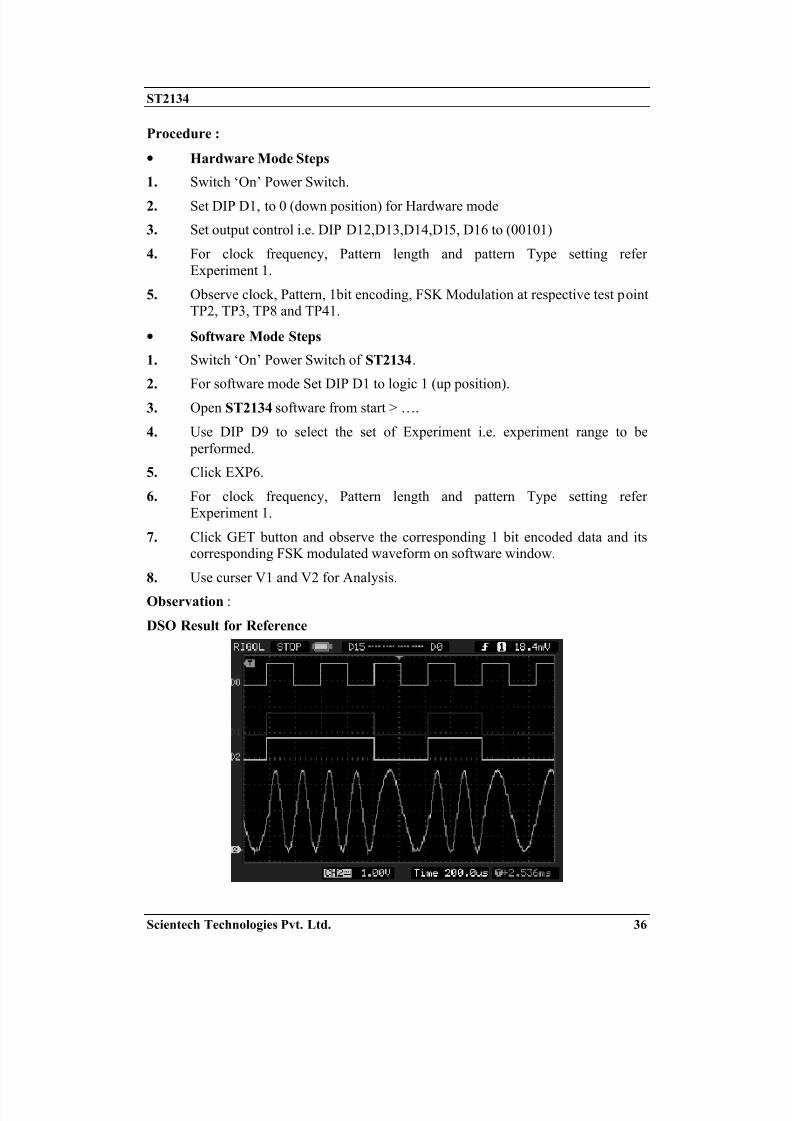
5. Observe clock, Pattern, 1bit encoding, ASK Modulation at respective test point TP2, TP3, TP8 and TP41.
• Software Mode Steps
1. Switch ‘On’ Power Switch of ST2134.
2. For software mode Set DIP D1 to logic 1 (up position)
3. Open ST2134 software from start > ….
4. Use DIP D9 to select the set of Experiment i.e. experiment range to be
performed.
5. Click EXP3.
6. For clock frequency, Pattern length and pattern Type setting refer
Experiment 1.
7. Click GET button and observe the corresponding 1 bit encoded data and itscorresponding ASK modulated waveform on software window.
8. Use curser V1 and V2 for Analysis.
Observation :
DSO Result for Reference

8/14/2019 ST2134 trainer kit manual
http://slidepdf.com/reader/full/st2134-trainer-kit-manual 23/171
ST2134
Scientech Technologies Pvt. Ltd. 23
Software Result for Reference
User Result :
1bit encoded data with ASK Modulation (first Set)

8/14/2019 ST2134 trainer kit manual
http://slidepdf.com/reader/full/st2134-trainer-kit-manual 24/171
ST2134
Scientech Technologies Pvt. Ltd. 24
1bit encoded data with ASK Modulation (Second Set)
Result :

8/14/2019 ST2134 trainer kit manual
http://slidepdf.com/reader/full/st2134-trainer-kit-manual 25/171
ST2134
Scientech Technologies Pvt. Ltd. 25
Experiment 4
Objective :
Study, Analysis and Measurement of BPSK Modulation with 1Bit Encoding
Theory :
In BPSK (Binary Shift Keying) Modulation, the phase of the carrier is varied to
represent binary 1 or 0. Both peak amplitude remains constant as the phase changes.
For example, if we start a phase of 0deg. to represent binary 1, then we can change the
phase to 180deg. to send binary 0. The phase of the signal during each bit duration is
constant, and its value depends on the bit (0 or 1).
Sin (2πft) for bit 0
Sin (2π/ft + π/) for bit 1
Sin (2π/ft) Sin (2π/ft + π/)
Figure below shows the generation of BPSK with clock signal, pattern or baseband
data, 1 bit encoded. Normal Sine wave or carrier is transmitted for logic 0 and 180o
phase shifted carrier is transmitted for logic 1.
Binary BPSK Modulated Signal
Figure 2

8/14/2019 ST2134 trainer kit manual
http://slidepdf.com/reader/full/st2134-trainer-kit-manual 26/171
ST2134
Scientech Technologies Pvt. Ltd. 26
Procedure :
• Hardware Mode Steps
1. Switch ‘On’ Power Switch.
2. Set DIP D1, to 0 (down position) for Hardware mode
3. Set output control i.e. DIP D12,D13,D14,D15, D16 to (00011)
4. For clock frequency, Pattern length and pattern Type setting refer
Experiment 1.
5. Observe clock, Pattern, 1bit encoding, BPSK Modulation at respective test point TP2, TP3, TP8 and TP41.
• Software Mode Steps
1. Switch ON Power Switch of ST2134.
2. For software mode Set DIP D1 to logic 1 (up position)
3. Open ST2134 software from start > ….
4. Use DIP D9 to select the set of Experiment i.e. experiment range to be
performed.
5. Click EXP4.
6. For clock frequency, Pattern length and pattern Type setting refer
Experiment 1.
7. Click GET button and observe the corresponding 1 bit encoded data and itscorresponding BPSK modulated waveform on software window.
8. Use curser V1 and V2 for Analysis.
Observation :
DSO Result for Reference

8/14/2019 ST2134 trainer kit manual
http://slidepdf.com/reader/full/st2134-trainer-kit-manual 27/171
ST2134
Scientech Technologies Pvt. Ltd. 27
Software Result for Reference
User Result :
1bit encoded data with BPSK Modulation (first Set)
1 bit encoded data with BPSK Modulation (Second Set)

8/14/2019 ST2134 trainer kit manual
http://slidepdf.com/reader/full/st2134-trainer-kit-manual 28/171
ST2134
Scientech Technologies Pvt. Ltd. 28
Result :

8/14/2019 ST2134 trainer kit manual
http://slidepdf.com/reader/full/st2134-trainer-kit-manual 29/171
ST2134
Scientech Technologies Pvt. Ltd. 29
Experiment 4A
Objective :
Study, Analysis and Measurement of DPSK Modulation with 1Bit Encoding
Theory :
Differential Encoding – Is used to provide polarity reversal protection
Bit streams going through the many communications circuits in the channel can be
un-intentionally inverted. Most signal processing circuits can not tell if the wholestream is inverted. This is also called phase ambiguity. Differential Encoding is used
to protect against this possibility. It is one of the simplest form of error protectioncoding done on a baseband sequence prior to modulation.
A Differential Coding system consists of a modulo 2 adder operation as shown below.
din = Data sequence in
eout = Differentially Encoded data sequence out
Encoding
+din eout
Eout = din + en-1
Here is how it works. Let’s take a sequence as shown below. The Encoding circuit
above has a reference bit (it can be 0 or 1, it doesn’t matter). The incoming data
sequence is added to this reference bit and forms the second bit of the encoded
sequence. This bit is then added to the next data bit to continue the process as shown
below.
In BPSK (Binary Shift Keying) Modulation, the phase of the carrier is varied to
represent binary 1 or 0. Both peak amplitude remains constant as the phase changes.
For example, if we start a phase of 0deg. to represent binary 1, then we can change the phase to 180deg. to send binary 0. The phase of the signal during each bit is constant,
and its value depends on the bit (0 or 1).

8/14/2019 ST2134 trainer kit manual
http://slidepdf.com/reader/full/st2134-trainer-kit-manual 30/171
ST2134
Scientech Technologies Pvt. Ltd. 30
Sin (2πft) for bit 0
Sin (2πft + π) for bit 1
Figure of Sin (2πft) Figure of Sin (2πft +π)
Figure below shows the generation of DPSK with clock signal, pattern or baseband
data, Differentially encoded data. Normal Sine wave or carrier is transmitted for logic
0 and 180o phase shifted carrier is transmitted for logic 1.
Figure : DPSK Modulated Signal
Procedure :
• Hardware Mode Steps
1. Switch ‘On’ Power Switch.
2. Set DIP D1, to 0 (down position) for Hardware mode
3. Set output control i.e. DIP D12,D13,D14,D15, D16 to (00100)
4. For clock frequency, Pattern length and pattern Type setting refer
Experiment 1.
5. Observe clock, Pattern, 1bit encoding, BPSK Modulation at respective test point TP2, TP3, TP8 and TP41.

8/14/2019 ST2134 trainer kit manual
http://slidepdf.com/reader/full/st2134-trainer-kit-manual 31/171
ST2134
Scientech Technologies Pvt. Ltd. 31
Observation :
DSO Result for Reference
User Result :
1bit encoded data with DPSK Modulation (first Set)
1bit encoded data with DPSK Modulation (Second Set)
Result :

8/14/2019 ST2134 trainer kit manual
http://slidepdf.com/reader/full/st2134-trainer-kit-manual 32/171
ST2134
Scientech Technologies Pvt. Ltd. 32
Experiment 5
Objective :
Study, Analysis and Measurement of BPSK Constellation
Theory :
A constellation is a plot of the symbols on the rectangular space. Visually the
constellation diagram which is what this picture is called, shows the phase of the
symbols and their relationship to each other. As in BPSK only one channel i.e.
baseband data is possible having logic level “1” or logic level “0”.
Constellation diagram for BPSK will look like figure as shown below. These two points shows that only 180o phase change is possible in BPSK.
Procedure :
• Hardware Mode Steps
1. Switch ‘On’ Power Switch.
2. Set DIP D1, to 0 (down position) for Hardware mode
3. Set output control i.e. DIP D12,D13,D14,D15, D16 to (00011)
4. For clock frequency, Pattern length and pattern Type setting refer
Experiment 1.
5. Set Oscilloscope in XY mode.
6. Connect BNC - Test Probe to channel 1 and Observe Constellation Pattern at
Test Point X1.

8/14/2019 ST2134 trainer kit manual
http://slidepdf.com/reader/full/st2134-trainer-kit-manual 33/171
ST2134
Scientech Technologies Pvt. Ltd. 33
• Software Mode Steps
1. Switch ‘On’ Power Switch of ST2134.
2. For software mode Set DIP D1 to logic 1 (up position).
3. Open ST2134 software from start > ….
4. Use DIP D9 to select the set of Experiment i.e. experiment range to be
performed.
5. Click EXP5.
6. Click GET button and observe the corresponding Constellation Pattern ofBPSK.
Observation :
DSO Result for Reference

8/14/2019 ST2134 trainer kit manual
http://slidepdf.com/reader/full/st2134-trainer-kit-manual 34/171

8/14/2019 ST2134 trainer kit manual
http://slidepdf.com/reader/full/st2134-trainer-kit-manual 35/171
ST2134
Scientech Technologies Pvt. Ltd. 35
Experiment 6
Objective :
Study, Analysis and Measurement of FSK Modulation with 1Bit Encoding
Theory :
In FSK Modulation, we change the frequency in response to information, one
particular frequency for Logic 1 and another frequency for Logic 0. In this example
below f1 for 1 is higher than f2 used for the 0 bit.
Sin(2πf1t) for bit 1
Sin(2πf2t) for bit 0
8/14/2019 ST2134 trainer kit manual
http://slidepdf.com/reader/full/st2134-trainer-kit-manual 36/171
ST2134
Scientech Technologies Pvt. Ltd. 36
Procedure :
• Hardware Mode Steps
1. Switch ‘On’ Power Switch.
2. Set DIP D1, to 0 (down position) for Hardware mode
3. Set output control i.e. DIP D12,D13,D14,D15, D16 to (00101)
4. For clock frequency, Pattern length and pattern Type setting refer
Experiment 1.
5. Observe clock, Pattern, 1bit encoding, FSK Modulation at respective test pointTP2, TP3, TP8 and TP41.
• Software Mode Steps
1. Switch ‘On’ Power Switch of ST2134.
2. For software mode Set DIP D1 to logic 1 (up position).
3. Open ST2134 software from start > ….
4. Use DIP D9 to select the set of Experiment i.e. experiment range to be
performed.
5. Click EXP6.
6. For clock frequency, Pattern length and pattern Type setting refer
Experiment 1.
7. Click GET button and observe the corresponding 1 bit encoded data and itscorresponding FSK modulated waveform on software window.
8. Use curser V1 and V2 for Analysis.
Observation :
DSO Result for Reference

8/14/2019 ST2134 trainer kit manual
http://slidepdf.com/reader/full/st2134-trainer-kit-manual 37/171
ST2134
Scientech Technologies Pvt. Ltd. 37
Software Result for Reference
User Result :
1bit encoded data with FSK Modulation (first Set)

8/14/2019 ST2134 trainer kit manual
http://slidepdf.com/reader/full/st2134-trainer-kit-manual 38/171
ST2134
Scientech Technologies Pvt. Ltd. 38
1bit encoded data with FSK Modulation (Second Set)
Result :

8/14/2019 ST2134 trainer kit manual
http://slidepdf.com/reader/full/st2134-trainer-kit-manual 39/171
ST2134
Scientech Technologies Pvt. Ltd. 39
Experiment 7
Objective :
Study, Analysis and Measurement of two bit encoding with pattern generator
and clock.Theory:
In two bit encoding techniques the incoming base band data stream is divided into two
data streams. Encoding is done in a manner that the rate of two new bit streams will
become half of that of the main baseband data.
Figure below shows the baseband data (01110110001111110) with respect to clockand two encoded bits i.e bit1 and bit2 having rates equals to half of the actual
baseband data. bit1 stream is also called as odd sequence as it is following odd valuesof the baseband data. Similarly bit 2 can be called as even bit stream as it is following
the even values of the incoming baseband data.
Procedure :
• Hardware Mode Steps
1. Switch ‘On’ Power Switch.
2. Set DIP D1, D2, D3, D4 to 0000.
3. Observe Clock frequency at test point TP2 with respect to Ground, it should
be 75 Hz.
4. Set DIP D1, D2, D3, D4 to 0001, 0010, 0011, 0100, 0101, 0110, 0111 andobserve their respective frequencies at test point TP2.
5. Set Output Control i.e. D12, D13, D14, D15, D16 (00110)
6. Set pattern length by using DIP D7, D8 (00 – 64 bits, 01 – 32 bits, 10 – 16
bits, 11 – 8 bits) and observe corresponding bit pattern at Test Point TP3.
7. For above Pattern Length you can select pattern type using DIP D5, D6 (00 –
Type 1, 01 – Type2, 10 – Type3, 11 – Type 4)]
8. Observe 2 bit encoded data at test point TP9 (bit1 - odd) and TP10 (bit2 -
even)
9. Observe the data rate of pattern at TP3 and rate of 2 bit encoded data at TP9,
TP10. (2 bit Encoded data should be half that of original pattern)

8/14/2019 ST2134 trainer kit manual
http://slidepdf.com/reader/full/st2134-trainer-kit-manual 40/171
ST2134
Scientech Technologies Pvt. Ltd. 40
• Software Mode Steps
1. Switch ‘On’ Power Switch of ST2134.
2. For software mode Set DIP D1 to logic 1 (up position).
3. Open ST2134 software from start > ….
4. Use DIP D9 to select the set of Experiment i.e. experiment range to be
performed.
5. Click EXP7.
6. Set DIP D2,D3,D4 from 000 to 111.
7. Set pattern length by using DIP D7,D8 (00 – 64 bits, 01 – 32 bits, 10 – 16 bits,
11 – 8 bits) of ST2134
8. For above Pattern Length you can select pattern type using DIP D5, D6 (00 –
Type 1, 01 – Type2, 10 – Type3, 11 – Type 4)
9. Click GET button and observe the corresponding clock, pattern, 2 bit encoding
(odd and even) on software window.
10. Use curser V1 and V2 for Analysis.
Observation :
DSO Result for Reference

8/14/2019 ST2134 trainer kit manual
http://slidepdf.com/reader/full/st2134-trainer-kit-manual 41/171
ST2134
Scientech Technologies Pvt. Ltd. 41
Software result for Reference
User Result (Hardware Mode) :
Clock
Pattern
Bit1 (odd)
Bit2 (even)
Clock
Pattern
Bit1 (odd)

8/14/2019 ST2134 trainer kit manual
http://slidepdf.com/reader/full/st2134-trainer-kit-manual 42/171
ST2134
Scientech Technologies Pvt. Ltd. 42
Bit2 (even)
Clock
Pattern
Bit1 (odd)
Bit2 (even)
Clock
Pattern
Bit1 (odd)
Bit2 (even)
Result :

8/14/2019 ST2134 trainer kit manual
http://slidepdf.com/reader/full/st2134-trainer-kit-manual 43/171
ST2134
Scientech Technologies Pvt. Ltd. 43
Experiment 8
Objective :
Study, Analysis and Measurement of QPSK Modulation with 2 Bit Encoding
Theory :
QPSK or Quadrature Phase Shift Keying, involves the splitting of a data stream mk (t)
= m0,m1,m2, . . ., into an in-phase stream or Even data m1 (t) = m0,m2,m4, . . . and a
quadrature stream or Odd data mQ(t) = m1,m3,m5, . . .. Both the streams have half
the bit rate of the data stream mk(t), and modulate the cosine and sine functions of a
carrier wave simultaneously. As a result, phase changes across intervals of 2Tb,
where Tb is the time interval of a single bit (the mk (t)s). The phase transitions can be
as large as ±180. Sudden phase reversals of ±180 can throw the amplifiers into
saturation. As shown in Figure 1, the phase reversals of ±180 cause the envelope to go
to zero momentarily. This may make us susceptible to non-linearity in amplifier
circuitry. The above may be prevented using linear amplifiers but they are more
expensive and power consuming. A solution to the above mentioned problem is theuse of OQPSK.
The two bit streams generated from 1/2bit encoding technique are used as I channel
data and Q channel data respectively for modulation of Cosine and Sine wave.
As is seen across the dotted line corresponding to a phase shift of , the envelop
reduces to zero temporarily

8/14/2019 ST2134 trainer kit manual
http://slidepdf.com/reader/full/st2134-trainer-kit-manual 44/171
ST2134
Scientech Technologies Pvt. Ltd. 44
QPSK modulated waveform is the linear sum of MOD1 and MOD2.
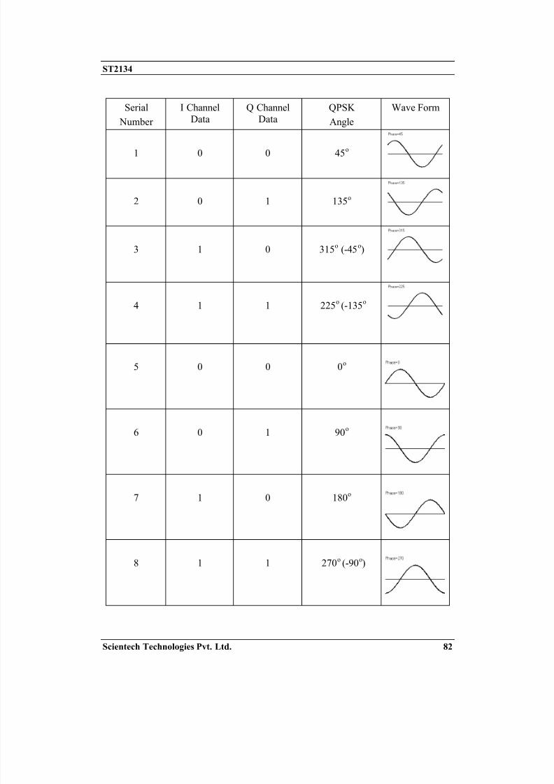
Final QPSK modulated wave will follow different angles for the combinations of I
channel and Q channel data as shown in the below Table.
Serial
Number
I ChannelData
Q ChannelData
QPSK
Angle
Wave Form
1 0 0 45o
2 0 1 135o
3 1 0 315o (-45
o)
4 1 1 225o(-135
o)
Note that in QPSK Modulated wave phase change in all condition is either +90o
or
+180o.

8/14/2019 ST2134 trainer kit manual
http://slidepdf.com/reader/full/st2134-trainer-kit-manual 45/171
ST2134
Scientech Technologies Pvt. Ltd. 45
Block Diagram for QPSK modulation is shown below
Procedure :
• Hardware Mode Steps
1. Switch ‘On’ Power Switch.
2. Set DIP D1, to 0 (down position) for Hardware mode
3. Set output control i.e. DIP D12,D13,D14,D15, D16 to (00111)
4. For clock frequency, Pattern length and pattern Type setting refer
Experiment 1.
5. Observe clock, Pattern, 2bit encoding (Even, Odd), I Channel Modulation, Q
Channel Modulation and QPSK Modulation at respective test points TP2, TP3,
TP9, TP10, TP39, TP40 and TP41.
• Software Mode Steps1. Switch ‘On’ Power Switch of ST2134.
2. For software mode Set DIP D1 to logic 1 (up position)
3. Open ST2134 software from start > ….
4. Use DIP D9 to select the set of Experiment i.e. experiment range to be
performed.
5. Click EXP8.
6. For clock frequency, Pattern length and pattern Type setting refer
Experiment 1.
7. Click GET button and observe the corresponding 2 bit encoded data and itscorresponding QPSK modulated waveform on software window.
8. Use curser V1 and V2 for Analysis.

8/14/2019 ST2134 trainer kit manual
http://slidepdf.com/reader/full/st2134-trainer-kit-manual 46/171
ST2134
Scientech Technologies Pvt. Ltd. 46
Observation :
DSO Result for Reference
Software Result for Reference

8/14/2019 ST2134 trainer kit manual
http://slidepdf.com/reader/full/st2134-trainer-kit-manual 47/171
ST2134
Scientech Technologies Pvt. Ltd. 47
User Result : :
Figure for Bit pattern
Figure for Symbol Pattern
Figure for I Channel Pattern
Figure for I Channel Modulation
Figure for Q Channel Pattern
Figure for Q Channel Modulation
Figure for QPSK Modulation.
Result :

8/14/2019 ST2134 trainer kit manual
http://slidepdf.com/reader/full/st2134-trainer-kit-manual 48/171
ST2134
Scientech Technologies Pvt. Ltd. 48
Experiment 9
Objective :
Study, Analysis and Measurement of QPSK Constellation
Theory :
A constellation is a plot of the symbols on the rectangular space. Visually the
constellation diagram, which is what this picture is called, shows the phase of the
symbols and their relationship to each other. As in QPSK two channel i.e. I Channel
and Q channels are available. I channel and Q channel are used to modulate
respectively Cosine and sine wave. The X-axis projection for each symbol is the I
channel amplitude and Y-axis projection is the Q channel Amplitude
Constellation diagram for QPSK will look like figure shown below.
As I Channel and Q Channel both can be either Logic “0” or Logic “1” so total fourcombination for (I,Q) are possible which are 00,01,10, and 11. The dark black lines
show all possible phase changes for QPSK Modulation.
Note that for QPSK Modulation +90o phase shift [(00-01), (01-11), (11-10) and (10-
00)] and +180o phase shift [(10-01), (00-11)] are possible.
Procedure :
• Hardware Mode Steps
1. Switch ‘On’ Power Switch.
2. Set DIP D1, to 0 (down position) for Hardware mode
3. Set output control i.e. DIP D12,D13,D14,D15, D16 to (01000)
4. For clock frequency, Pattern length and pattern Type setting refer
Experiment 1.
5. Set Oscilloscope in XY mode.
6. Connect BNC to Test Probe to channel 1, channel 2 and Observe Constellation
Pattern respectively at Test Point X2, Test Point Y2.

8/14/2019 ST2134 trainer kit manual
http://slidepdf.com/reader/full/st2134-trainer-kit-manual 49/171
ST2134
Scientech Technologies Pvt. Ltd. 49
• Software Mode Steps
1. Switch ‘On’ Power Switch of ST2134.
2. For software mode Set DIP D1 to logic 1 (up position)
3. Open ST2134 software from start > ….
4. Use DIP D9 to select the set of Experiment i.e. experiment range to be
performed.
5. Click EXP 9.
6. Click GET button and observe the corresponding Constellation Pattern ofQPSK.
Observation :
DSO Result for Reference

8/14/2019 ST2134 trainer kit manual
http://slidepdf.com/reader/full/st2134-trainer-kit-manual 50/171
ST2134
Scientech Technologies Pvt. Ltd. 50
Software Result for Reference
User Result (Hardware Mode) :
Result :

8/14/2019 ST2134 trainer kit manual
http://slidepdf.com/reader/full/st2134-trainer-kit-manual 51/171
ST2134
Scientech Technologies Pvt. Ltd. 51
Experiment 10
Objective :
Study, Analysis and Measurement of Rate 1/2 Convolutional Encoding
Theory :
Convolutional Encoding-
Convolutional codes are commonly specified by three parameters; (n, k, m).
n = number of output bits
k = number of input bits
m = number of memory registers
The quantity k/n called the code rate is a measure of the efficiency of the code.
Commonly k and n parameters range from 1 to 8, m from 2 to 10 and the code ratefrom 1/8 to 7/8 except for deep space applications where code rates as low as 1/100 or
even longer have been employed.
Often the manufacturers of convolutional code chips specify the code by parameters
(n,k,L), The quantity L is called the constraint length of the code and is defined by
Constraint Length, L = k (m-1)
The constraint length L represents the number of bits in the encoder memory thataffect the generation of the n output bits. The constraint length L is also referred to by
the capital letter K, which can be confusing with the lower case k, which representsthe number of input bits. In some books K is defined as equal to product the of k and
m. Often in commercial spec, the codes are specified by (r, K), where r = the code ratek/n and K is the constraint length. The constraint length K however is equal to L - 1,
as defined in this paper. I will be referring to convolutional codes as (n, k, m) and notas (r, K).
Code parameters and the structure of the convolutional code :
The convolutional code structure is easy to draw from its parameters. First draw m
boxes representing the m memory register. Then draw n modulo-2 adders to represent
the n output bits.
Now connect the memory registers to the adders using the generator polynomial as
shown in the figure below.

8/14/2019 ST2134 trainer kit manual
http://slidepdf.com/reader/full/st2134-trainer-kit-manual 52/171
ST2134
Scientech Technologies Pvt. Ltd. 52
This (3, 1, 3) convolutional code has 3 memory registers, 1 input bit and 3 output bits.
This is a rate 1/3 code. Each input bit is coded into 3 output bits. The constraint lengthof the code is 2. The 3 output bits are produced by the 3 modulo-2 adders by adding
up certain bits in the memory registers. The selection of which bits are to be added to
produce the output bit is called the generator polynomial (g) for that output bit. For
example, the first output bit has a generator polynomial of (1, 1, 1). The output bit 2
has a generator polynomial of (0, 1, 1) and the third output bit has a polynomial of (1,0, 1). The output bits just the sum of these bits.
v1 = mod2 (u1 + u0 + u-1)
v2 = mod2 (u0 + u-1)
v3 = mod2 (u1 + u-1)
The polynomials give the code its unique error protection quality. One (3,1,4) codecan have completely different properties from an another one depending on the
polynomials chosen.
How polynomials are selected :
There are many choices for polynomials for any m order code. They do not all result
in output sequences that have good error protection properties. Petersen and Weldon’s
book contains a complete list of these polynomials. Good polynomials are found from
this list usually by computer simulation. A list of good polynomials for rate ½ codes
is given below.
Table 1-Generator Polynomials found by Busgang for good rate ½ codes
Constraint Length G1 G2
3 110 111
4 1101 1110
5 11010 11101

8/14/2019 ST2134 trainer kit manual
http://slidepdf.com/reader/full/st2134-trainer-kit-manual 53/171
ST2134
Scientech Technologies Pvt. Ltd. 53
6 110101 111011
7 110101 110101
8 110111 1110011
9 110111 111001101
10 110111001 1110011001
States of a Code :
We have states of mind and so do encoders. We are depressed one day, and perhapshappy the next from the many different states we can be in. Our output depends on
our states of mind and tongue in-cheek we can say that encoders too act this way.
What they output depends on what is their state of mind. Our states are complex but
encoder states are just a sequence of bits. Sophisticated encoders have long constraint
lengths and simple ones have short in dicating the number of states they can be in the(2,1,4) code in Figure below has a constraint length of 3. The shaded registers below
hold these bits. The unshaded register holds the incoming bit. This means that 3 bits
or 8 different combination of these bits can be present in these memory registers.
These 8 different combinations determine what output we will get for v1 and v2, the
coded sequence.
The number of combinations of bits in the shaded registers are called the states of the
code and are defined by Number of states = 2L where L = the constraint length of the
code and is equal to L = k (m - 1).
The states of a code indicate what is in the memory registers think of states as sort of
an initial condition. The output bit depends on this initial condition, which changes at
each time tick.
Let’s examine the states of the code (2,1,4) shown above. This code outputs 2 bits forevery 1 input bit. It is a rate ½ codes. Its constraint length is 3. The total number of
states is equal to 8. The eight states of this (2,1,4) code are: 000, 001, 010, 011, 100,101, 110, 111.

8/14/2019 ST2134 trainer kit manual
http://slidepdf.com/reader/full/st2134-trainer-kit-manual 54/171
ST2134
Scientech Technologies Pvt. Ltd. 54
State Table for Rate = ½
Input Bit Input states Output Bits Output states
I1 SI1 SI2 SI3 V1 V2 SO1 SO2 SO3
0 0 0 0 0 0 0 0 0
1 0 0 0 1 1 1 0 0
0 0 0 1 1 1 0 0 0
1 0 0 1 0 0 1 0 0
0 0 1 0 1 0 0 0 1
1 0 1 0 0 1 1 0 1
0 0 1 1 0 1 0 0 1
1 0 1 1 1 0 1 0 1
0 1 0 0 1 1 0 1 0
1 1 0 0 0 0 1 1 0
0 1 0 1 0 0 0 1 0
1 1 0 1 1 1 1 1 0
0 1 1 0 0 1 0 1 1
1 1 1 0 1 0 1 1 1
0 1 1 1 1 0 0 1 1
1 1 1 1 0 1 1 1 1
Procedure :
• Hardware Mode Steps
1. Switch ‘On’ Power Switch.
2. Set DIP D1, D2, D3, D4 to 0000.
3. Observe Clock frequency at test point TP2 with respect to Ground, it should
be 75Hz.
4. Set DIP D1, D2, D3, D4 to 0001, 0010, 0011, 0100, 0101, 0110, 0111 and
observe their respective frequencies at test point TP2.
5. Set Output Control i.e. D12, D13, D14, D15, D16 (01001)
6. Set pattern length by using DIP D7, D8 (00 – 64 bits, 01 – 32 bits, 10 – 16
bits, 11 – 8 bits) and observe corresponding bit pattern at Test Point TP3.
7. For above Pattern Length you can select pattern type using DIP D5, D6 (00 –Type 1, 01 – Type2, 10 – Type3, 11 – Type 4)]

8/14/2019 ST2134 trainer kit manual
http://slidepdf.com/reader/full/st2134-trainer-kit-manual 55/171
ST2134
Scientech Technologies Pvt. Ltd. 55
8. Observe 1/2 bit encoded data at test point TP11 (bit1) and TP12 (bit2)
9. Observe the data rate of pattern at TP3 and rate of 2 bit encoded data at TP11,
TP12. (1/2 rate convolutional Encoded data should be same that of original
pattern)• Software Mode Steps
1. Switch ‘On’ Power Switch of ST2134.
2. For software mode Set DIP D1 to logic 1 (up position)
3. Open ST2134 software from start > ….
4. Use DIP D9 to select the set of Experiment i.e. experiment range to be
performed.
5. Click EXP10.
6. Set DIP D2, D3, D4 from 000 to 111.
7. Set pattern length by using DIP D7,D8 (00 – 64 bits, 01 – 32 bits, 10 – 16 bits,
11 – 8 bits) of ST2134
8. For above Pattern Length you can select pattern type using DIP D5, D6 (00 –
Type 1, 01 – Type2, 10 – Type3, 11 – Type 4)
9. Click GET button and observe the corresponding clock, pattern, 1/2 rate
convolutional encoding (bit1 and bit2) on software window.
10. Use curser V1 and V2 for Analysis.
Observation :
DSO Result for Reference

8/14/2019 ST2134 trainer kit manual
http://slidepdf.com/reader/full/st2134-trainer-kit-manual 56/171
ST2134
Scientech Technologies Pvt. Ltd. 56
Software result for Reference
User Result (Hardware Mode) :
Clock
Pattern
Bit1
Bit2
Clock
Pattern
Bit1
Bit2

8/14/2019 ST2134 trainer kit manual
http://slidepdf.com/reader/full/st2134-trainer-kit-manual 57/171
ST2134
Scientech Technologies Pvt. Ltd. 57
Clock
Pattern
Bit1
Bit2
Clock
Pattern
Bit1
Bit2
Result :

8/14/2019 ST2134 trainer kit manual
http://slidepdf.com/reader/full/st2134-trainer-kit-manual 58/171
ST2134
Scientech Technologies Pvt. Ltd. 58
Experiment 11
Objective :
Study, Analysis and Measurement of QPSK Modulation with rate 1/2 Bit
EncodingTheory :
QPSK or Quadrature Phase Shift Keying, involves the splitting of a data stream mk(t)
= m0,m1,m2, . . ., into an in-phase stream or Even data mI (t) = m0,m2,m4, . . . and a
quadrature stream or Odd data mQ(t) = m1,m3,m5, . . .. Both the streams have half
the bit rate of the data stream mk(t), and modulate the cosine and sine functions of a
carrier wave simultaneously. As a result, phase changes across intervals of 2Tb,
where Tb is the time interval of a single bit (the mk (t)s). The phase transitions can be
as large as ±180. Sudden phase reversals of ±180 can throw the amplifiers into
saturation. As shown in figure below the phase reversals of ±180 cause the envelope
to go to zero momentarily. This may make us susceptible to non-linearity in amplifier
circuitry. The above may be prevented using linear amplifiers but they are moreexpensive and power consuming. A solution to the above-mentioned problem is the
use of OQPSK.
The two bit streams generated from 1/2bit encoding technique are used as I channel
data and Q channel data respectively for modulation of Cosine and Sine wave.
As is seen across the dotted line corresponding to a phase shift of , the envelop
reduces to zero temporarily
QPSK Modulation process in rate ½ encoding will remains the same as in QPSK
using 2 bit encoding. Figure below shows clock, input data or baseband data, outputdata of state machine, MOD1, MOD2, QPSK.
Output data shown below is in two bit format having both I channel and Q Channel
data.Here only input and output data are shown and the state analysis can be done using
look-up given in Experiment 10.

8/14/2019 ST2134 trainer kit manual
http://slidepdf.com/reader/full/st2134-trainer-kit-manual 59/171
ST2134
Scientech Technologies Pvt. Ltd. 59
QPSK Modulation with rate ½ Encoding
Final QPSK modulated wave will follow different angles for the combinations of I
channel and Q channel data as shown in the below Table.
Serial
Number
I Channel
Data
Q Channel
Data
QPSK
Angle
Wave Form
1 0 0 45o
2 0 1 135o
3 1 0 315o (-45o)
4 1 1 225o
(-135o)
Note that in QPSK Modulated wave phase change in all condition is either +90o
or
+180o.

8/14/2019 ST2134 trainer kit manual
http://slidepdf.com/reader/full/st2134-trainer-kit-manual 60/171
ST2134
Scientech Technologies Pvt. Ltd. 60
Block Diagram for QPSK modulation is shown below
Procedure :
• Hardware Mode Steps
1. Switch ‘On’ Power Switch.
2. Set DIP D1, to 0 (down position) for Hardware mode
3. Set output control i.e. DIP D12,D13,D14,D15, D16 to (01010)
4. For clock frequency, Pattern length and pattern Type setting referExperiment 1.
5. Observe clock, Pattern, 1/2bit encoding (bit1, bit2), I Channel Modulation, Q
Channel Modulation and QPSK Modulation at respective test points TP2, TP3,
TP11, TP12, TP39, TP40 and TP41.
• Software Mode Steps
1. Switch ON Power Switch of ST2134.
2. For software mode Set DIP D1 to logic 1 (up position).
3. Open ST2134 software from start > ….
4. Use DIP D9 to select the set of Experiment i.e. experiment range to be
performed.
5. Click EXP11.
6. For clock frequency, Pattern length and pattern Type setting referExperiment 1.
7. Click GET button and observe the corresponding 1/2 rate convolutionalencoded data and its corresponding QPSK modulated waveform on software
window.
8. Use curser V1 and V2 for Analysis.

8/14/2019 ST2134 trainer kit manual
http://slidepdf.com/reader/full/st2134-trainer-kit-manual 61/171
ST2134
Scientech Technologies Pvt. Ltd. 61
Observation :
DSO Result for Reference
Software Result for Reference
User Result :

8/14/2019 ST2134 trainer kit manual
http://slidepdf.com/reader/full/st2134-trainer-kit-manual 62/171
ST2134
Scientech Technologies Pvt. Ltd. 62
Figure for Bit pattern
Figure for Symbol Pattern
Figure for I Channel Pattern
Figure for I Channel Modulation
Figure for Q Channel Pattern
Figure for Q Channel Modulation
Figure for QPSK Modulation.
Result :

8/14/2019 ST2134 trainer kit manual
http://slidepdf.com/reader/full/st2134-trainer-kit-manual 63/171
ST2134
Scientech Technologies Pvt. Ltd. 63
Experiment 12
Objective :
Study, Analysis and Measurement of OQPSK Modulation with 2 Bit Encoding
Theory :
As shown in Experiment 8 & 11. Taking four values of the phase (two bits) at a time
to construct a QPSK symbol can allow the phase of the signal to jump by as much as
180° at a time. This produces large amplitude fluctuations in the signal; an
undesirable quality in communication systems. A solution to the above mentioned
problem is the use of OQPSK. In OQPSK by offsetting the timing of the odd and even
bits by one bit-period, or half a symbol-period, the in-phase and quadrature
components will never change at the same time.
OQPSK modulation is such that phase transitions about the origin are avoided. The
scheme is used in IS-95 handsets. In OQPSK the pulse streams mI (t) = m0,m2,m4, . .. and mQ(t) = m1,m3,m5, . . . are offset in alignment, in other words are staggered, by
one bit period (half a symbol period). Figure 3 [2], shows the staggering of the datastreams in time. Figure 4 [1], shows the OQPSK waveform undergoing a phase shift
of ± π /2. The result of limiting the phase shifts to ± π /2 is that the envelope will notgo to zero as it does with QPSK.
Figure 3
The figure shows the staggering of the in phase and quadrature modulated data
streams in OQPSK. The staggering restricts the phase changes to ±90 as shown in
figure 4.
In OQPSK, the phase transitions take place every Tb seconds. In QPSK the transitionstake place every 2Tb seconds.

8/14/2019 ST2134 trainer kit manual
http://slidepdf.com/reader/full/st2134-trainer-kit-manual 64/171
ST2134
Scientech Technologies Pvt. Ltd. 64
Figure 4
The figure shows a QPSK waveform. As is seen across the dotted lines the phase
changes are of ± π /2.
The two-bit streams generated from 2bit encoding technique i.e. Odd pattern and
Even Patternused as I channel data and Q channel data respectively for modulation ofCosine and Sine wave.
OQPSK modulated waveform is the linear sum of MOD1 and MOD2.
Final QPSK modulated wave will follow different angles for the combinations of Ichannel and Q channel data as shown in the below Table.

8/14/2019 ST2134 trainer kit manual
http://slidepdf.com/reader/full/st2134-trainer-kit-manual 65/171
ST2134
Scientech Technologies Pvt. Ltd. 65
Serial
Number
I Channel
Data
Q Channel
Data
QPSK
Angle
Wave Form
1 0 0 45o
2 0 1 135o
3 1 0 315o (-45
o)
4 1 1 225o (-135o)
Note that in QPSK Modulated wave phase change in all condition is either +90o or
+180o.
Block Diagram for OQPSK modulation is shown below

8/14/2019 ST2134 trainer kit manual
http://slidepdf.com/reader/full/st2134-trainer-kit-manual 66/171
ST2134
Scientech Technologies Pvt. Ltd. 66
Procedure :
• Hardware Mode Steps
1. Switch ‘On’ Power Switch.
2. Set DIP D1, to 0 (down position) for Hardware mode
3. Set output control i.e. DIP D12,D13,D14,D15, D16 to (01011)
4. For clock frequency, Pattern length and pattern Type setting refer
Experiment 1.
5. Observe clock, Pattern, 2bit encoding (Even, Odd), OQPSK encoded (even,odd) I Channel Modulation, Q Channel Modulation and OQPSK Modulation
at respective test points TP2, TP3, TP9, TP10, TP27, TP28, TP39, TP40 and
TP41.
• Software Mode Steps
1. Switch ‘On’ Power Switch of ST2134.
2. For software mode Set DIP D1 to logic 1 (up position)
3. Open ST2134 software from start > ….
4. Use DIP D9 to select the set of Experiment i.e. experiment range to be
performed.
5. Click EXP12.
6. For clock frequency, Pattern length and pattern Type setting refer
Experiment 1.
7. Click GET button and observe the corresponding OQPSK encoded data and its
corresponding OQPSK modulated waveform on software window.8. Use curser V1 and V2 for Analysis.
Observation :
DSO Result for Reference

8/14/2019 ST2134 trainer kit manual
http://slidepdf.com/reader/full/st2134-trainer-kit-manual 67/171
ST2134
Scientech Technologies Pvt. Ltd. 67
Software Result for Reference

8/14/2019 ST2134 trainer kit manual
http://slidepdf.com/reader/full/st2134-trainer-kit-manual 68/171
ST2134
Scientech Technologies Pvt. Ltd. 68
User Result : :
Figure for Bit pattern
Figure for Symbol Pattern
Figure for I Channel Pattern
Figure for I Channel Modulation
Figure for Q Channel Pattern

8/14/2019 ST2134 trainer kit manual
http://slidepdf.com/reader/full/st2134-trainer-kit-manual 69/171
ST2134
Scientech Technologies Pvt. Ltd. 69
Figure for Q Channel Modulation
Figure for OQPSK Modulation.
Result :

8/14/2019 ST2134 trainer kit manual
http://slidepdf.com/reader/full/st2134-trainer-kit-manual 70/171
ST2134
Scientech Technologies Pvt. Ltd. 70
Experiment 13
Objective :
Study, Analysis and Measurement of OQPSK Constellation
Theory :
A constellation is a plot of the symbols on the rectangular space. Visually the
constellation diagram which is what this picture is called, shows the phase of the
symbols and their relationship to each other.
In the constellation diagram shown on the left, it can be seen that this will limit the
phase-shift to no more than 90° at a time. This yields much lower amplitude
fluctuations than non-offset QPSK and is often preferred in practice.
The picture on the left shows the constellation for OQPSK. As I Channel and Q
Channel both can be either Logic “0” or Logic “1” so total four combination for I & Qare possible which are 00,01,10, and 11. or Four different levels are possible as shown
in the multilevel signal on the right.
The dark black lines show all possible phase changes for OQPSK Modulation.
Note that for OQPSK Modulation only +90o phase shift [(00-01), (01-11), (11-10)
and (10-00)] are possible.
The picture on the right shows the difference in the behavior of the phase betweenordinary QPSK and OQPSK. It can be seen that in the first plot the phase can change
by 180° at once, while in OQPSK the changes are never greater than 90°.

8/14/2019 ST2134 trainer kit manual
http://slidepdf.com/reader/full/st2134-trainer-kit-manual 71/171
ST2134
Scientech Technologies Pvt. Ltd. 71
Procedure :
• Hardware Mode Steps
1. Switch ‘On’ Power Switch.
2. Set DIP D1, to 0 (down position) for Hardware mode
3. Set output control i.e. DIP D12,D13,D14,D15, D16 to (01100)
4. For clock frequency, Pattern length and pattern Type setting refer
Experiment 1.
5. Set Oscilloscope in XY mode.
6. Connect BNC to Test Probe to channel 1, channel 2 and Observe Constellation
Pattern respectively at Test Point X3, Test Point Y3.
• Software Mode Steps
1. Switch ‘On’ Power Switch of ST2134.
2. For software mode Set DIP D1 to logic 1 (up position)
3. Open ST2134 software from start >….
4. Use DIP D9 to select the set of Experiment i.e. experiment range to be performed.
5. Click EXP 13.
6. Click GET button and observe the corresponding Constellation Pattern of
OQPSK.
Observation :
DSO Result for Reference

8/14/2019 ST2134 trainer kit manual
http://slidepdf.com/reader/full/st2134-trainer-kit-manual 72/171
ST2134
Scientech Technologies Pvt. Ltd. 72
Software Result for Reference
User Result (Hardware Mode) :
Result :

8/14/2019 ST2134 trainer kit manual
http://slidepdf.com/reader/full/st2134-trainer-kit-manual 73/171
ST2134
Scientech Technologies Pvt. Ltd. 73
Experiment 14
Objective :
Study, Analysis and Measurement of OQPSK Modulation with rate 1/2 Bit
EncodingTheory :
OQPSK or offset Quadrature Phase Shift Keying, involves the splitting of a data
stream mk(t) = m0,m1,m2, . . ., into an in-phase stream or Even data mI (t) =
m0,m2,m4, . . . and a quadrature stream or Odd data mQ(t) = m1,m3,m5, . . .. Both
the streams have half the bit rate of the data stream mk(t), and modulate the cosine
and sine functions of a carrier wave simultaneously. As a result, phase changes across
intervals of 2Tb, where Tb is the time interval of a single bit (the mk(t)s). The phase
transitions can be as large as ±180. Sudden phase reversals of ±180 can throw the
amplifiers into saturation. As shown in figure 5, the phase reversals of ±180 cause the
envelope to go to zero momentarily. This may make us susceptible to non-linearity in
amplifier circuitry. The above may be prevented using linear amplifiers but they aremore expensive and power consuming. A solution to the above mentioned problem is
the use of OQPSK.
The two bit streams generated from 1/2bit encoding technique are used as I channel
data and Q channel data respectively for modulation of Cosine and Sine wave.
Figure 5
As is seen across the dotted line corresponding to a phase shift of , the envelopreduces to zero temporarily
OQPSK Modulation process in rate ½ encoding will remains the same as in OQPSK
using 2 bit encoding. Figure below shows clock, input data or baseband data, outputdata of state machine, MOD1, MOD2, QPSK.
Output data shown below is in two bit format having both I channel and Q Channel
data.
Here only input and output data are shown and the state analysis can be done using
look-up given in Experiment 10.

8/14/2019 ST2134 trainer kit manual
http://slidepdf.com/reader/full/st2134-trainer-kit-manual 74/171
ST2134
Scientech Technologies Pvt. Ltd. 74
OQPSK Modulation with rate ½ Encoding Figure 6
Final QPSK modulated wave will follow different angles for the combinations of I
channel and Q channel data as shown in the below Table.
Serial
Number
I Channel
Data
Q Channel
Data
QPSK
Angle
Wave Form
1 0 0 45o
2 0 1 135o
3 1 0 315o (-45
o)
4 1 1 225o(-135
o)
Note that in OQPSK Modulated wave phase change in all condition is +90o.
Block Diagram for OQPSK modulation is shown below

8/14/2019 ST2134 trainer kit manual
http://slidepdf.com/reader/full/st2134-trainer-kit-manual 75/171
ST2134
Scientech Technologies Pvt. Ltd. 75
Procedure :
• Hardware Mode Steps
1. Switch ‘On’ Power Switch.
2. Set DIP D1, to 0 (down position) for Hardware mode
3. Set output control i.e. DIP D12,D13,D14,D15, D16 to (01101)
4. For clock frequency, Pattern length and pattern Type setting refer
Experiment 1.
5. Observe clock, Pattern, 1/2bit encoding (bit1, bit2), OQPSK encoded
(bit1,bit2), I Channel Modulation, Q Channel Modulation and QPSKModulation at respective test points TP2, TP3, TP11, TP12, TP27, TP28,
TP39, TP40 and TP41.
• Software Mode Steps1. Switch ‘On’ Power Switch of ST2134.
2. For software mode Set DIP D1 to logic 1 (up position)
3. Open ST2134 software from start > ….
4. Use DIP D9 to select the set of Experiment i.e. experiment range to be
performed.
5. Click EXP14.
6. For clock frequency, Pattern length and pattern Type setting refer
Experiment 1.
7. Click GET button and observe the corresponding 1/2 rate convolutionalencoded data and its corresponding OQPSK modulated waveform on softwarewindow.
8. Use curser V1 and V2 for Analysis.

8/14/2019 ST2134 trainer kit manual
http://slidepdf.com/reader/full/st2134-trainer-kit-manual 76/171
ST2134
Scientech Technologies Pvt. Ltd. 76
Observation :
DSO Result for Reference
Software Result for Reference

8/14/2019 ST2134 trainer kit manual
http://slidepdf.com/reader/full/st2134-trainer-kit-manual 77/171
ST2134
Scientech Technologies Pvt. Ltd. 77
User Result :
Figure for Bit pattern
Figure for Symbol Pattern
Figure for I Channel Pattern
Figure for I Channel Modulation
Figure for Q Channel Pattern
Figure for Q Channel Modulation
Figure for QPSK Modulation.
Result :

8/14/2019 ST2134 trainer kit manual
http://slidepdf.com/reader/full/st2134-trainer-kit-manual 78/171
ST2134
Scientech Technologies Pvt. Ltd. 78
Experiment 15
Objective :
Study, Analysis and Measurement of π/4 QPSK Modulation with 2 Bit Encoding
Theory :
Like QPSK, π/4-QPSK transmits two bits per symbol. So only four carrier signals are
needed but this is where the twist comes in. In QPSK we have four signals that are
used to send the four twobit symbols. In π/4-QPSK we have eight signals, every
alternate symbol is transmitted using a π/4 shifted pattern of the QPSP constellation.Symbol A uses a signal on Path A as shown below and the next symbol, B, even if it
is exactly the same bit pattern uses a signal on Path B. So we always get a phase shift
even when the adjacent symbols are exactly the same.
The constellation diagram looks similar to 8-PSK. Note that a 8-PSK constellation
can be broken into two QPSK constellations as show below. In π/4-QPSK, onesymbol is transmitted on the A constellation and the next one is transmitted using
the B constellation. Even though on a network analyzer, the constellation lookslike 8-PSK, this modulation is strictly a form of QPSK with same BER and
bandwidth. Although the symbols move around, they always convey just 2 bits
per symbol.
Figure 41 - π/4-QPSK constellation mimics 8-PSK but it is two QPSK constellationsthat are phase shifted.
Step-by-step π/4-QPSK
We wish to transmit the following bit sequence
. 0 0 0 0 1 0 0 0 0 1 1 1 1 1 0 0 0 1 0 0odd 0 0 1 0 0 1 1 0 0 0
even 0 0 0 0 1 1 1 0 1 0

8/14/2019 ST2134 trainer kit manual
http://slidepdf.com/reader/full/st2134-trainer-kit-manual 79/171

8/14/2019 ST2134 trainer kit manual
http://slidepdf.com/reader/full/st2134-trainer-kit-manual 80/171
ST2134
Scientech Technologies Pvt. Ltd. 80
I and Q mapping of π/4-QPSK symbols Figure 7
Step 1 - Map bits to symbols
Bits 00 00 10 00 01 11 11 00 01 00
Symbols A1 B1 A4 B1 A2 B2 A3 B1 A2 B3
Step 2 - Multiply the I and Q with a carrier (in the example below, the carrier
frequency is 1 Hz.) and you get an 8-PSK signal constellation.
π/4-QPSK symbols traverse over a 8-PSK constellation
Figure 8
The constellation diagram is a path that the symbols have traced in time as we can see
in the above diagram of just the symbols of this signal. The path stars with symbolA1, then goes to B1, which is on path B. From here, the next symbol A2 is back on
Path A. Each transition, we see above goes back and forth between Path A and B.

8/14/2019 ST2134 trainer kit manual
http://slidepdf.com/reader/full/st2134-trainer-kit-manual 81/171
ST2134
Scientech Technologies Pvt. Ltd. 81
π/4-QPSK modulated I and Q ChannelsFigure 9
π/4-QPSK modulated carrier
Figure 10
What is the advantage of doing this? On the average, the phase transitions are
somewhat less than a straight QPSK and this does two things, one is that the side
lobes are smaller so less adjacent carrier interference. Secondly the response to Class
C amplifiers is better. This modulation is used in many mobile systems.
There is also a modification to this modulation where a differential encoding is added
to the bits prior to modulation. (More about differential encoding in Tutorial 2) When
differential coding is added, the modulation is referred to as π/4-DQPSK.
Final π/4 QPSK modulated wave will follow different angles for the combinations ofI channel and Q channel data as shown in the below Table.
8/14/2019 ST2134 trainer kit manual
http://slidepdf.com/reader/full/st2134-trainer-kit-manual 82/171
ST2134
Scientech Technologies Pvt. Ltd. 82
Serial
Number
I Channel
Data
Q Channel
Data
QPSK
Angle
Wave Form
1 0 0 45o
2 0 1 135o
3 1 0 315o (-45
o)
4 1 1 225o
(-135o
5 0 0 0o
6 0 1 90o
7 1 0 180o
8 1 1 )270o(-90
o

8/14/2019 ST2134 trainer kit manual
http://slidepdf.com/reader/full/st2134-trainer-kit-manual 83/171
ST2134
Scientech Technologies Pvt. Ltd. 83
Note that in QPSK Modulated wave phase change in all condition is either +90o or
+180o.
Block Diagram for QPSK modulation is shown below
Procedure :
• Hardware Mode Steps
1. Switch ‘On’ Power Switch.
2. Set DIP D1, to 0 (down position) for Hardware mode
3. Set output control i.e. DIP D12,D13,D14,D15, D16 to (01110)
4. For clock frequency, Pattern length and pattern Type setting referExperiment 1.
5. Observe clock, Pattern, 2bit encoding (Even, Odd), I Channel Modulation, Q
Channel Modulation and π/4 QPSK Modulation at respective test points TP2,TP3, TP9, TP10, TP39, TP40 and TP41.
• Software Mode Steps
1. Switch ‘On’ Power Switch of ST2134.
2. For software mode Set DIP D1 to logic 1 (up position)
3. Open ST2134 software from start > ….
4. Use DIP D9 to select the set of Experiment i.e. experiment range to be
performed.
5. Click EXP15.
6. For clock frequency, Pattern length and pattern Type setting refer
Experiment 1.
7. Click GET button and observe the corresponding 2 bit encoded data and itscorresponding QPSK modulated waveform on software window.
8. Use curser V1 and V2 for Analysis.

8/14/2019 ST2134 trainer kit manual
http://slidepdf.com/reader/full/st2134-trainer-kit-manual 84/171
ST2134
Scientech Technologies Pvt. Ltd. 84
Observation :
DSO Result for Reference
Software Result for Reference

8/14/2019 ST2134 trainer kit manual
http://slidepdf.com/reader/full/st2134-trainer-kit-manual 85/171
ST2134
Scientech Technologies Pvt. Ltd. 85
User Result :
Figure for Bit pattern
Figure for Symbol Pattern
Figure for I Channel Pattern
Figure for I Channel Modulation
Figure for Q Channel Pattern
Figure for Q Channel Modulation
Figure for π/4 QPSK Modulation.
Result :

8/14/2019 ST2134 trainer kit manual
http://slidepdf.com/reader/full/st2134-trainer-kit-manual 86/171
ST2134
Scientech Technologies Pvt. Ltd. 86
Experiment 16
Objective :
Study, of π/4 QPSK Constellation and eye pattern
Theory :
The constellation diagram looks similar to 8-PSK. Note that a 8-PSK constellationcan be broken into two QPSK constellations as show below in figure. In π/4-QPSK,
one symbol is transmitted on the A constellation and the next one is transmitted using
the B constellation. In reality when for constellation pattern on Oscilloscope both path
A and path B overlaps each other and we get constellation similar to that of QPSK.
The π/4 QPSK differ with QPSK in number of phase shift in the final modulated
wave. In comparison to QPSK here in π/4 QPSK we will get 8 phase shift.
Procedure :• Hardware Mode Steps
1. Switch ‘On’ Power Switch.
2. Set DIP D1, to 0 (down position) for Hardware mode
3. Set output control i.e. DIP D12,D13,D14,D15, D16 to (01111)
4. For clock frequency, Pattern length and pattern Type setting refer
Experiment 1.
5. Set Oscilloscope in XY mode.
6. Connect BNC to Test Probe to channel 1, channel 2 and Observe Constellation
Pattern respectively at Test Point X4, Test Point Y4.

8/14/2019 ST2134 trainer kit manual
http://slidepdf.com/reader/full/st2134-trainer-kit-manual 87/171
ST2134
Scientech Technologies Pvt. Ltd. 87
• Software Mode Steps
1. Switch ‘On’ Power Switch of ST2134.
2. For software mode Set DIP D1 to logic 1 (up position).
3. Open ST2134 software from start > ….
4. Use DIP D9 to select the set of Experiment i.e. experiment range to be
performed.
5. Click EXP 16.
6. Click GET button and observe the corresponding Constellation Pattern of π/4QPSK.
Observation :
DSO Result for Reference

8/14/2019 ST2134 trainer kit manual
http://slidepdf.com/reader/full/st2134-trainer-kit-manual 88/171
ST2134
Scientech Technologies Pvt. Ltd. 88
Software Result for Reference
User Result (Hardware Mode) :
Result :

8/14/2019 ST2134 trainer kit manual
http://slidepdf.com/reader/full/st2134-trainer-kit-manual 89/171
ST2134
Scientech Technologies Pvt. Ltd. 89
Experiment 17
Objective :
Study, Analysis and Measurement of π/4 QPSK Modulation with rate 1/2 Bit
Encoding
Theory :
Like QPSK, π/4-QPSK transmits two bits per symbol. So only four carrier signals areneeded but this is where the twist comes in. In QPSK, we have four signals that are
used to send the four twobit symbols. In π/4-QPSK, we have eight signals; every
alternate symbol is transmitted using a π/4 shifted pattern of the QPSP constellation.Symbol A uses a signal on Path A as shown below and the next symbol, B, even if it
is exactly the same bit pattern uses a signal on Path B. So we always get a phase shifteven when the adjacent symbols are exactly the same.
The constellation diagram looks similar to 8-PSK. Note that a 8-PSK constellation
can be broken into two QPSK constellations as show below. In π/4-QPSK, one
symbol is transmitted on the A constellation and the next one is transmitted usingthe B constellation. Even though on a network analyzer, the constellation looks
like 8-PSK, this modulation is strictly a form of QPSK with same BER and
bandwidth. Although the symbols move around, they always convey just 2 bits
per symbol.
Figure 11
π /4-QPSK constellat ion mimi cs 8-PSK bu t i t is two QPSK constellat ions that ar e
phase shi ft ed .
Step-by-step π/4-QPSK :
We wish to transmit the following bit sequence. We divide the bit sequence into 2-bit pieces just as we would do for QPSK. Now for π/4 QPSK using ½ encoding. We
Bit sequence: 00 00 10 00 01 11 11 00 01 00
Transmit the first symbol using the A constellation shown in Figure 11 and the next
symbol uses the B constellation. For each 2-bit, the I and Q values are the signalcoordinates as shown below.

8/14/2019 ST2134 trainer kit manual
http://slidepdf.com/reader/full/st2134-trainer-kit-manual 90/171
ST2134
Scientech Technologies Pvt. Ltd. 90
Table 5 - π/4-QPSK symbols mapping to I and Q
The I and Q channels for a π/4-QPSK signal are shown below in figure 12. Note that
there are five possible levels (1, .707. 0 -.707, -1) and I and the Q channel show thisvariation in response to the symbols
I and Q mapping of π/4-QPSK symbols Figure 12
Step 1 - Map bits to symbolsBits 00 00 10 00 01 11 11 00 01 00
Symbols A1 B1 A4 B1 A2 B2 A3 B1 A2 B3
Step 2 - Multiply the I and Q with a carrier (in the example below, the carrier
frequency is 1 Hz.) and you get an 8-PSK signal constellation.

8/14/2019 ST2134 trainer kit manual
http://slidepdf.com/reader/full/st2134-trainer-kit-manual 91/171
ST2134
Scientech Technologies Pvt. Ltd. 91
π/4-QPSK symbols traverse over a 8-PSK constellation
Figure 13
The constellation diagram is a path that the symbols have traced in time as we can seein the above diagram of just the symbols of this signal. The path stars with symbol
A1, then goes to B1 which is on path B. From here, the next symbol A2 is back onPath A. Each transition, we see above goes back and forth between Path A and B.
π/4-QPSK modulated I and Q Channels
Figure 14

8/14/2019 ST2134 trainer kit manual
http://slidepdf.com/reader/full/st2134-trainer-kit-manual 92/171
ST2134
Scientech Technologies Pvt. Ltd. 92
π/4-QPSK modulated carrier
Figure 15
What is the advantage of doing this? On the average, the phase transitions are
somewhat less than a straight QPSK and this does two things, one is that the sidelobes are smaller so less adjacent carrier interference. Secondly, the response to Class
C amplifiers is better. This modulation is used in many mobile systems.
There is also a modification to this modulation where a differential encoding is added
to the bits prior to modulation. (More about differential encoding in Tutorial 2) When
differential coding is added, the modulation is referred to as π/4-DQPSK.
Final π/4 QPSK modulated wave will follow different angles for the combinations of
I channel and Q channel data as shown in the below Table.
Serial
Number
I Channel
Data
Q Channel
Data
QPSK
Angle
Wave Form
1 0 0 45o
2 0 1 135o
3 1 0 315o (-45
o)

8/14/2019 ST2134 trainer kit manual
http://slidepdf.com/reader/full/st2134-trainer-kit-manual 93/171
ST2134
Scientech Technologies Pvt. Ltd. 93
4 1 1 225o (-135o)
5 0 0 0o
6 0 1 90o
7 1 0 180o
8 1 1 270o
(-90o
oro
90+ion is either Note that in QPSK Modulated wave phase change in all condit
.o
180+
Block Diagram for QPSK modulation is shown below

8/14/2019 ST2134 trainer kit manual
http://slidepdf.com/reader/full/st2134-trainer-kit-manual 94/171
ST2134
Scientech Technologies Pvt. Ltd. 94
Procedure :
• Hardware Mode Steps
1. Switch ‘On’ Power Switch.
2. Set DIP D1, to 0 (down position) for Hardware mode
3. Set output control i.e. DIP D12,D13,D14,D15, D16 to (10000)
4. For clock frequency, Pattern length and pattern Type setting refer
Experiment 1.
5. Observe clock, Pattern, 1/2bit encoding (bit1, bit2), I Channel Modulation, Q
Channel Modulation and π/4 QPSK Modulation at respective test points TP2,
TP3, TP11, TP12, TP39, TP40 and TP41.
• Software Mode Steps
1. Switch ‘On’ Power Switch of ST2134.
2. For software mode Set DIP D1 to logic 1 (up position).
3. Open ST2134 software from start > ….
4. Use DIP D9 to select the set of Experiment i.e. experiment range to be performed.
5. Click EXP17.
6. For clock frequency, Pattern length and pattern Type setting refer
Experiment 1.
7. Click GET button and observe the corresponding 1/2 rate convolutional
encoded data and its corresponding QPSK modulated waveform on software
window.
8. Use curser V1 and V2 for Analysis.

8/14/2019 ST2134 trainer kit manual
http://slidepdf.com/reader/full/st2134-trainer-kit-manual 95/171
ST2134
Scientech Technologies Pvt. Ltd. 95
Observation :
DSO Result for Reference
Software Result for Reference

8/14/2019 ST2134 trainer kit manual
http://slidepdf.com/reader/full/st2134-trainer-kit-manual 96/171
ST2134
Scientech Technologies Pvt. Ltd. 96
User Result :
Figure for Bit pattern
Figure for Symbol Pattern
Figure for I Channel Pattern
Figure for I Channel Modulation
Figure for Q Channel Pattern
Figure for Q Channel Modulation
Figure for π/4 QPSK Modulation.
Result :

8/14/2019 ST2134 trainer kit manual
http://slidepdf.com/reader/full/st2134-trainer-kit-manual 97/171
ST2134
Scientech Technologies Pvt. Ltd. 97
Experiment 18
Objective :
Study, Analysis and Measurement of three bit encoding with pattern generator
and clock.
Theory :
In three bit encoding techniques the incoming base band data stream is divided into
three data streams. Encoding is done in a manner that the rate of three new bit streamswill become 1/3 of that of the main baseband data.
Figure below shows the baseband data (01110110001111110) with respect to clock
and three encoded bits i.e bit1, bit2, bit3 having rates equals to one third of the actual
baseband data.
Procedure:
• Hardware Mode Steps
1. Switch ‘On’ Power Switch.
2. Set DIP D1, D2, D3, D4 to 0000.
3.
Observe Clock frequency at test point TP2 with respect to Ground, it should be 75Hz.
4. Set DIP D1, D2, D3, D4 to 0001, 0010, 0011, 0100, 0101, 0110, 0111 and
observe their respective frequencies at test point TP2.
5. Set Output Control i.e. D12, D13, D14, D15, D16 (10001)
6. Set pattern length by using DIP D7, D8 (00 – 64 bits, 01 – 32 bits, 10 – 16
bits, 11 – 8 bits) and observe corresponding bit pattern at Test Point TP3.
7. For above Pattern Length you can select pattern type using DIP D5, D6 (00 –
Type 1, 01 – Type2, 10 – Type3, 11 – Type 4)]
8. Observe 3 bit encoded data at test point TP13 (bit1), TP14 (bit2) and TP15
(bit3)
9. Observe the data rate of pattern at TP3 and rate of 3 bit encoded data at TP13,
TP14 and TP15. (3 bit Encoded data should be one third that of original
pattern)

8/14/2019 ST2134 trainer kit manual
http://slidepdf.com/reader/full/st2134-trainer-kit-manual 98/171
ST2134
Scientech Technologies Pvt. Ltd. 98
• Software Mode Steps
1. Switch ‘On’ Power Switch of ST2134.
2. For software mode Set DIP D1 to logic 1 (up position)
3. Open ST2134 software from start > ….
4. Use DIP D9 to select the set of Experiment i.e. experiment range to be
performed.
5. Click EXP18.
6. Set DIP D2,D3,D4 from 000 to 111.
7. Set pattern length by using DIP D7,D8 (00 – 64 bits, 01 – 32 bits, 10 – 16 bits,
11 – 8 bits) of ST2134
8. For above Pattern Length you can select pattern type using DIP D5, D6 (00 –
Type 1, 01 – Type2, 10 – Type3, 11 – Type 4)
9. Click GET button and observe the corresponding clock, pattern, 2 bit encoding
(odd and even) on software window.
10. Use curser V1 and V2 for Analysis.
Observation :
DSO Result for Reference

8/14/2019 ST2134 trainer kit manual
http://slidepdf.com/reader/full/st2134-trainer-kit-manual 99/171
ST2134
Scientech Technologies Pvt. Ltd. 99
Software result for Reference
User Result (Hardware Mode) :
Clock
Pattern
Bit1
Bit2
Bit3
Clock
Pattern
Bit1

8/14/2019 ST2134 trainer kit manual
http://slidepdf.com/reader/full/st2134-trainer-kit-manual 100/171
ST2134
Scientech Technologies Pvt. Ltd. 100
Bit2
Bit3
Clock
Pattern
Bit1
Bit2
Bit3
Clock
Pattern
Bit1
Bit2
Bit3
Result :

8/14/2019 ST2134 trainer kit manual
http://slidepdf.com/reader/full/st2134-trainer-kit-manual 101/171
ST2134
Scientech Technologies Pvt. Ltd. 101
Experiment 19
Objective :
Study, Analysis and Measurement of 8-PSK modulation with three bit encoding,
pattern generator and clock.Theory :
In three bit encoding techniques the incoming base band data stream is divided into
three data streams. Encoding is done in a manner that the rate of three new bit streams
will become 1/3 of that of the main baseband data.
Figure below shows the baseband data (01110110001111110) with respect to clockand three encoded bits i.e BIT1, BIT2, BIT3 having rates equals to one and half of the
actual baseband data.
In case of 8-PSK we have two basic functions again, a Sine and a Cosine and eachconfiguration has a different phase to indicate a specific bit pattern.
In 8-PSK we have eight different phases
Table shown below :3 bit Encoded Data CosWct SinWct Composite Signal
000 0.924 -0.383 Cos(Wct + π/8)
001 0.383 -0.924 Cos(Wct + 3π/8)
010 -0.383 -0.924 Cos(Wct + 5π/8)
011 -0.924 -0.383 Cos(Wct + 7π/8)
100 -0.924 0.383 Cos(Wct - 7π/8)
101 -0.383 0.924 Cos(Wct – 5π/8)
110 0.383 0.924 Cos(Wct – 3π/8)
111 0.924 0.383 Cos(Wct - π/8)
Actually, two multilevel baseband signals need to be established: one for the in-pahse
(I) Signal and one for the out-of-phase ( Q ) signal. These baseband signals are
referred to as mI(t) and mQ(t) for the I and Q signals, respectively. The level chosen

8/14/2019 ST2134 trainer kit manual
http://slidepdf.com/reader/full/st2134-trainer-kit-manual 102/171
ST2134
Scientech Technologies Pvt. Ltd. 102
for the two baseband signals correspond to the coefficients needed to represent a PSK
signal as a linear combination of the I and Q signals. Below figure shows how an 8-
PSK signal, defined in above table can be generated by adding two amplitude-
modulated signals.
8-PSK Modulation (Block Diagram)
Procedure :
• Hardware Mode Steps
1. Switch ‘On’ Power Switch.
2. Set DIP D1, to 0 (down position) for Hardware mode
3. Set output control i.e. DIP D12,D13,D14,D15, D16 to (10010)
4. For clock frequency, Pattern length and pattern Type setting refer
Experiment 1.
5. Observe clock, Pattern, 3bit encoding (bit1, bit2, bit3), I Channel Modulation,
Q Channel Modulation and 8PSK Modulation at respective test points TP2,
TP3, TP13, TP14, TP15, TP39, TP40 and TP41.
• Software Mode Steps
1. Switch ‘On’ Power Switch of ST2134.
2. For software mode Set DIP D1 to logic 1 (up position).
3. Open ST2134 software from start > ….
4. Use DIP D9 to select the set of Experiment i.e. experiment range to be
performed.
5. Click EXP19.
6. For clock frequency, Pattern length and pattern Type setting refer
Experiment 1.

8/14/2019 ST2134 trainer kit manual
http://slidepdf.com/reader/full/st2134-trainer-kit-manual 103/171
ST2134
Scientech Technologies Pvt. Ltd. 103
7. Click GET button and observe the corresponding 3 bit encoded data and its
corresponding 8PSK modulated waveform on software window.
8. Use curser V1 and V2 for Analysis.

8/14/2019 ST2134 trainer kit manual
http://slidepdf.com/reader/full/st2134-trainer-kit-manual 104/171
ST2134
Scientech Technologies Pvt. Ltd. 104
Observation :
DSO Result for Reference
Software Result for Reference

8/14/2019 ST2134 trainer kit manual
http://slidepdf.com/reader/full/st2134-trainer-kit-manual 105/171
ST2134
Scientech Technologies Pvt. Ltd. 105
User Result :
Figure for Bit pattern
Figure for Symbol Pattern
Figure for I Channel Pattern
Figure for I Channel Modulation
Figure for Q Channel Pattern
Figure for Q Channel Modulation
Figure for 8PSK Modulation.
Result :

8/14/2019 ST2134 trainer kit manual
http://slidepdf.com/reader/full/st2134-trainer-kit-manual 106/171
ST2134
Scientech Technologies Pvt. Ltd. 106
Experiment 20
Objective :
Study of 8 PSK Constellation and eye pattern
Theory :
8-PSK ConstellationIn 8-PSK constellation there are 8 points on the circle with phase difference of 45 deg.
With this modulator 3 bits are processed to produce a single phase change. This
means that each symbol consists of 3 bits. The constellation for this modulator
scheme is shown below
Procedure :
• Hardware Mode Steps
1. Switch ‘On’ Power Switch.
2. Set DIP D1, to 0 (down position) for Hardware mode
3. Set output control i.e. DIP D12,D13,D14,D15, D16 to (10011)
4. For clock frequency, Pattern length and pattern Type setting refer
Experiment 1.
5. Set Oscilloscope in XY mode.
6. Connect BNC to Test Probe to channel 1, channel 2 and Observe Constellation
Pattern respectively at Test Point X5, Test Point Y5.
• Software Mode Steps
1. Switch ‘On’ Power Switch of ST2134.
2. For software mode Set DIP D1 to logic 1 (up position)
3. Open ST2134 software from start > ….4. Use DIP D9 to select the set of Experiment i.e. experiment range to be
performed.
5. Click EXP 20.
6. Click GET button and observe the corresponding Constellation Pattern of
8PSK.

8/14/2019 ST2134 trainer kit manual
http://slidepdf.com/reader/full/st2134-trainer-kit-manual 107/171
ST2134
Scientech Technologies Pvt. Ltd. 107
Observation :
DSO Result for Reference
Software Result for Reference

8/14/2019 ST2134 trainer kit manual
http://slidepdf.com/reader/full/st2134-trainer-kit-manual 108/171
ST2134
Scientech Technologies Pvt. Ltd. 108
User Result (Hardware Mode)
Result :

8/14/2019 ST2134 trainer kit manual
http://slidepdf.com/reader/full/st2134-trainer-kit-manual 109/171
ST2134
Scientech Technologies Pvt. Ltd. 109
Experiment 21
Objective :
Study, Analysis and Measurement of rate 2/3 convolution encoding
Theory :
Convolution Encoding-
Convolution codes are commonly specified by three parameters; (n,k,m).
n = number of output bits
k = number of input bits
m = number of memory registers
The quantity k/n called the code rate, is a measure of the efficiency of the code.
Commonly k and n parameters range from 1 to 8, m from 2 to 10 and the code ratefrom 1/8 to 7/8 except for deep space applications where code rates as low as 1/100 or
even longer have been employed.
Often the manufacturers of convolutional code chips specify the code by parameters
(n,k,L), The quantity L is called the constraint length of the code and is defined by
Constraint Length, L = k (m-1)
The constraint length L represents the number of bits in the encoder memory thataffect the generation of the n output bits. The constraint length L is also referred to by
the capital letter K, which can be confusing with the lower case k, which representsthe number of input bits. In some books K is defined as equal to the product of k and
m. Often in commercial spec, the codes are specified by (r, K), where r = the code ratek/n and K is the constraint length. The constraint length K however is equal to L - 1,
as defined in this paper. I will be referring to convolutional codes as (n,k,m) and notas (r,K).
Code parameters and the structure of the convolutional code :
The convolutional code structure is easy to draw from its parameters. First draw m
boxes representing the m memory registers. Then draw n modulo-2 adders to
represent the n output bits. Now connect the memory registers to the adders using the
generator polynomial as shown in the figure 16.
Figure 16

8/14/2019 ST2134 trainer kit manual
http://slidepdf.com/reader/full/st2134-trainer-kit-manual 110/171
ST2134
Scientech Technologies Pvt. Ltd. 110
This (3,1,3) convolutional code has 3 memory registers, 1 input bit and 3 outputbits.
This is a rate 1/3 code. Each input bit is coded into 3 output bits. The constraint length
of the code is 2. The 3 output bits are produced by the 3 modulo-2 adders by addingup certain bits in the memory registers. The selection of which bits are to be added to
produce the output bit is called the generator polynomial (g) for that output bit. For
example, the first output bit has a generator polynomial of (1,1,1). The output bit 2
has a generator polynomial of (0,1,1) and the third output bit has a polynomial of
(1,0,1). The output bits just the sum of these bits.
v1 = mod2 (u1 + u0 + u-1)
v2 = mod2 ( u0 + u-1)
v3 = mod2 (u1 + u-1)
The polynomials give the code its unique error protection quality. One (3,1,4) code
can have completely different properties from an another one depending on the polynomials chosen.
How polynomials are selected :
There are many choices for polynomials for any m order code. They do not all resultin output sequences that have good error protection properties. Petersen and Weldon’s
book contains a complete list of these polynomials. Good polynomials are found fromthis list usually by computer simulation. A list of good polynomials for rate ½ codes
is given below.
Table 1-Generator Polynomials found by Busgang for good rate ½ codes
States of a code :
We have states of mind and so do encoders. We are depressed one day, and perhapshappy the next from the many different states we can be in. Our output depends on
our states of mind and tongue in-cheek we can say that encoders too act this way.
What they output depends on what is their state of mind. Our states are complex but
encoder states are just a sequence of bits. Sophisticated encoders have long constraint
lengths and simple ones have short in dicating the number of states they can be in.

8/14/2019 ST2134 trainer kit manual
http://slidepdf.com/reader/full/st2134-trainer-kit-manual 111/171
ST2134
Scientech Technologies Pvt. Ltd. 111
The (2,1,4) code in figure 17 has a constraint length of 3. The shaded registers below
hold these bits. The unshaded register holds the incoming bit. This means that 3 bits
or 8 different combinations of these bits can be present in these memory registers.
These 8 different combinations determine what output we will get for v1 and v2, the
coded sequence.
The number of combinations of bits in the shaded registers are called the states of the
code and are defined by Number of states = 2L where L = the constraint length of the
code and is equal to L = k (m - 1).
The states of a code indicate what is in the memory registers
Figure 17
Think of states as sort of an initial condition. The output bit depends on this initial
condition which changes at each time tick.
Let’s examine the states of the code (3,2,2) shown above. This code outputs 3 bits for
every 2 input bit. It is a rate 2/3 code. Its constraint length is 2. The total number of
states is equal to 4. The eight states of this (3,2,2) code are: 00, 01, 10, 11 for different
combinations of 2 bit inputs
State Table for Rate = 2/3
Input Bit Input
states
Output Bits Output states
Even odd SI1 SI2 V1 V2 V3 SO1 SO2
00 0 0 0 0 0 0 0
01 0 0 0 1 1 0 1
10 0 0 1 0 1 1 0
11 0 0 1 1 0 1 1
00 0 1 0 1 0 0 001 0 1 0 0 1 0 1
10 0 1 1 1 1 1 0
11 0 1 1 0 0 1 1
00 1 0 1 0 0 0 0

8/14/2019 ST2134 trainer kit manual
http://slidepdf.com/reader/full/st2134-trainer-kit-manual 112/171
ST2134
Scientech Technologies Pvt. Ltd. 112
01 1 0 1 1 1 0 1
10 1 0 0 0 1 1 0
11 1 0 0 1 0 1 1
00 1 1 1 1 0 0 0
01 1 1 1 0 1 0 1
10 1 1 0 1 1 1 0
11 1 1 0 0 0 1 1
State machine used for 2/3 bit encoding is shown below
Consider a input bit stream 011110 and initial state is S0 i.e. 00
The first information block is 01, causing the encoder to transit from S0 to S1 andoutput coded word is 01
Now encoder is at state S1. The next information block is 11, causing the encoder to
transit from S1 to S3 and coded output word is 100.
Similarly for the next information block 10, current state is S3, encoder causing state
change from S3 to S2 and output coded word is 011.
Procedure:
• Hardware Mode Steps
1. Switch ‘On’ Power Switch.
2.
Set DIP D1, D2, D3, D4 to 0000.3. Observe Clock frequency at test point TP2 with respect to Ground, it should
be 75Hz.
4. Set DIP D1, D2, D3, D4 to 0001, 0010, 0011, 0100, 0101, 0110, 0111 and
observe their respective frequencies at test point TP2.
5. Set Output Control i.e. D12, D13, D14, D15, D16 (10100)

8/14/2019 ST2134 trainer kit manual
http://slidepdf.com/reader/full/st2134-trainer-kit-manual 113/171
ST2134
Scientech Technologies Pvt. Ltd. 113
6. Set pattern length by using DIP D7, D8 (00 – 64 bits, 01 – 32 bits, 10 – 16
bits, 11 – 8 bits) and observe corresponding bit pattern at Test Point TP3.
7. For above Pattern Length you can select pattern type using DIP D5, D6 (00 –
Type 1, 01 – Type2, 10 – Type3, 11 – Type 4)]8. Observe Pattern out, 2 bit encoding, 2/3convolutional encoding at test point
TP3, TP9, TP10, TP16, TP17, TP18 and verify the results with state table
shown above.
• Software Mode Steps
1. Switch ‘On’ Power Switch of ST2134.
2. For software mode Set DIP D1 to logic 1 (up position).
3. Open ST2134 software from start > ….
4. Use DIP D9 to select the set of Experiment i.e. experiment range to be performed.
5. Click EXP21.
6. Set DIP D2,D3,D4 from 000 to 111 and set output control DIP D12, D13,
D14, D15, D16 to 10100.
7. Set pattern length by using DIP D7,D8 (00 – 64 bits, 01 – 32 bits, 10 – 16 bits,
11 – 8 bits) of ST2134
8. For above Pattern Length you can select pattern type using DIP D5, D6 (00 –
Type 1, 01 – Type2, 10 – Type3, 11 – Type 4)
9. Click GET button and observe the corresponding clock, pattern, 2 bit encoding
(odd and even), rate 2/3 convolutional encoding on software window.
10. Use curser V1 and V2 for Analysis.
Observation :
DSO Result for Reference

8/14/2019 ST2134 trainer kit manual
http://slidepdf.com/reader/full/st2134-trainer-kit-manual 114/171
ST2134
Scientech Technologies Pvt. Ltd. 114
Software result for Reference
User Result (Hardware Mode) :
Clock
Pattern
Even
Odd
Current
state
Next state
Bit1

8/14/2019 ST2134 trainer kit manual
http://slidepdf.com/reader/full/st2134-trainer-kit-manual 115/171
ST2134
Scientech Technologies Pvt. Ltd. 115
Bit2
Bit3
Clock
Pattern
Even
Odd
Currentstate
Next state
Bit1
Bit2
Bit3
Clock
Pattern
Even
Odd
Currentstate

8/14/2019 ST2134 trainer kit manual
http://slidepdf.com/reader/full/st2134-trainer-kit-manual 116/171
ST2134
Scientech Technologies Pvt. Ltd. 116
Next state
Bit1
Bit2
Bit3
Clock
Pattern
Even
Odd
Currentstate
Next state
Bit1
Bit2
Bit3
Result :

8/14/2019 ST2134 trainer kit manual
http://slidepdf.com/reader/full/st2134-trainer-kit-manual 117/171
ST2134
Scientech Technologies Pvt. Ltd. 117
Experiment 22
Objective :
Study, Analysis and Measurement of 8-PSK modulation with rate 2/3
convolutional encoding, pattern generator and clockTheory :
2/3 Convolutioanl Encoding-
Convolutional codes are commonly specified by three parameters; (n,k,m).
n = number of output bits
k = number of input bits
m = number of memory registers
The quantity k/n called the code rate, is a measure of the efficiency of the code.Commonly k and n parameters range from 1 to 8, m from 2 to 10 and the code rate
from 1/8 to 7/8 except for deep space applications where code rates as low as 1/100 oreven longer have been employed.
Often the manufacturers of convolutional code chips specify the code by parameters
(n,k,L), The quantity L is called the constraint length of the code and is defined by
Constraint Length, L = k (m-1)
The constraint length L represents the number of bits in the encoder memory that
affect the generation of the n output bits. The constraint length L is also referred to bythe capital letter K, which can be confusing with the lower case k, which represents
the number of input bits. In some books K is defined as equal to the product of k andm. Often in commercial spec, the codes are specified by (r, K), where r = the code rate
k/n and K is the constraint length. The constraint length K however is equal to L - 1,as defined in this paper. I will be referring to convolutional codes as (n,k,m) and not
as (r,K).
Code parameters and the structure of the convolutional code :
The convolutional code structure is easy to draw from its parameters. First draw m
boxes representing the m memory registers. Then draw n modulo-2 adders to
represent the n output bits. Now connect the memory registers to the adders using the
generator polynomial as shown in the figure 18.
Figure 18

8/14/2019 ST2134 trainer kit manual
http://slidepdf.com/reader/full/st2134-trainer-kit-manual 118/171
ST2134
Scientech Technologies Pvt. Ltd. 118
This (3,1,3) convolutional code has 3 memory registers, 1 input bit and 3 output bits.
This is a rate 1/3 code. Each input bit is coded into 3 output bits. The constraint length
of the code is 2. The 3 output bits are produced by the 3 modulo-2 adders by adding
up certain bits in the memory registers. The selection of which bits are to be added to produce the output bit is called the generator polynomial (g) for that output bit. For
example, the first output bit has a generator polynomial of (1,1,1). The output bit 2
has a generator polynomial of (0,1,1) and the third output bit has a polynomial of
(1,0,1). The output bits just the sum of these bits.
v1 = mod2 (u1 + u0 + u-1)
v2 = mod2 ( u0 + u-1)
v3 = mod2 (u1 + u-1)
The polynomials give the code its unique error protection quality. One (3,1,4) code
can have completely different properties from an another one depending on the
polynomials chosen.How polynomials are selected :
There are many choices for polynomials for any m order code. They do not all result
in output sequences that have good error protection properties. Petersen and Weldon’s book contains a complete list of these polynomials. Good polynomials are found from
this list usually by computer simulation. A list of good polynomials for rate ½ codesis given below.
Table 1-Generator Polynomials found by Busgang for good rate ½ codes
States of a code :
We have states of mind and so do encoders. We are depressed one day, and perhaps
happy the next from the many different states we can be in. Our output depends onour states of mind and tongue in-cheek we can say that encoders too act this way.
What they output depends on what is their state of mind. Our states are complex butencoder states are just a sequence of bits. Sophisticated encoders have long constraint
lengths and simple ones have short indicating the number of states they can be in.
The (2,1,4) code in figure 19 has a constraint length of 3. The shaded registers below
hold these bits. The unshaded register holds the incoming bit. This means that 3 bits
or 8 different combinations of these bits can be present in these memory registers.

8/14/2019 ST2134 trainer kit manual
http://slidepdf.com/reader/full/st2134-trainer-kit-manual 119/171
ST2134
Scientech Technologies Pvt. Ltd. 119
These 8 different combinations determine what output we will get for v1 and v2, the
coded sequence.
The number of combinations of bits in the shaded registers are called the states of the
code and are defined by Number of states = 2
L
where L = the constraint length of thecode and is equal to L = k (m - 1).
Figure 19
The states of a code indicate what is in the memory registers think of states as sort of
an initial condition. The output bit depends on this initial condition which changes ateach time tick.
Let’s examine the states of the code (3,2,2) shown above. This code outputs 3 bits for
every 2 input bit. It is a rate 2/3 code. Its constraint length is 2. The total number of
states is equal to 4. The eight states of this (3,2,2) code are: 00, 01, 10, 11 for different
combinations of 2 bit inputs
State Table for Rate = 2/3
Input Bit Input
states
Output Bits Output states
Even odd SI1 SI2 V1 V2 V3 SO1 SO200 0 0 0 0 0 0 0
01 0 0 0 1 1 0 1
10 0 0 1 0 1 1 0
11 0 0 1 1 0 1 1
00 0 1 0 1 0 0 0
01 0 1 0 0 1 0 1
10 0 1 1 1 1 1 0
11 0 1 1 0 0 1 1
00 1 0 1 0 0 0 0
01 1 0 1 1 1 0 1
10 1 0 0 0 1 1 0
11 1 0 0 1 0 1 1

8/14/2019 ST2134 trainer kit manual
http://slidepdf.com/reader/full/st2134-trainer-kit-manual 120/171
ST2134
Scientech Technologies Pvt. Ltd. 120
00 1 1 1 1 0 0 0
01 1 1 1 0 1 0 1
10 1 1 0 1 1 1 0
11 1 1 0 0 0 1 1
State machine used for 2/3 bit encoding is shown below
Consider a input bit stream 011110 and initial state is S0 i.e. 00
The first information block is 01, causing the encoder to transit from S0 to S1 and
output coded word is 01
Now encoder is at state S1. The next information block is 11, causing the encoder totransit from S1 to S3 and coded output word is 100.
Similarly for the next information block 10, current state is S3, encoder causing state
change from S3 to S2 and output coded word is 011.

8/14/2019 ST2134 trainer kit manual
http://slidepdf.com/reader/full/st2134-trainer-kit-manual 121/171
ST2134
Scientech Technologies Pvt. Ltd. 121
Theory :
8-PSK
In case of 8-PSK we have two basic functions again, a Sine and a Cosine and each
configuration has a different phase to indicate a specific bit pattern.
In 8-PSK we have eight different phases.
Table shown below :
3 bit Encoded
Data
CosWct SinWct Composite Signal
000 0.924 -0.383 Cos(Wct + π/8)
001 0.383 -0.924 Cos(Wct + 3π/8)
010 -0.383 -0.924 Cos(Wct + 5π/8)
011 -0.924 -0.383 Cos(Wct + 7π/8)
100 -0.924 0.383 Cos(Wct - 7π/8)
101 -0.383 0.924 Cos(Wct – 5π/8)
110 0.383 0.924 Cos(Wct – 3π/8)
111 0.924 0.383 Cos(Wct - π/8)
Actually, two multilevel baseband signals need to be established: one for the in-pahse(I)
Signal and one for the out-of-phase ( Q ) signal. These baseband signals are referred
to as mI(t) and mQ(t) for the I and Q signals, respectively. The level chosen for the
two baseband signals correspond to the coefficients needed to represent a PSK signal
as a linear combination of the I and Q signals. Below figure 19 shows how an 8-PSK
signal, defined in above table can be generated by adding two amplitude-modulated
signals.

8/14/2019 ST2134 trainer kit manual
http://slidepdf.com/reader/full/st2134-trainer-kit-manual 122/171
ST2134
Scientech Technologies Pvt. Ltd. 122
PSK Modulation (Block Diagram) Figure 19
Procedure :
• Hardware Mode Steps
1. Switch ‘On’ Power Switch.
2. Set DIP D1, to 0 (down position) for Hardware mode
3. Set output control i.e. DIP D12,D13,D14,D15, D16 to (10101)
4. For clock frequency, Pattern length and pattern Type setting referExperiment 1.
5. Observe clock, Pattern, 2 bit encoding, 2/3 rate convolutional encoding (bit1,
bit2, bit3), I Channel Modulation, Q Channel Modulation and 8PSK
Modulation at respective test points TP2, TP3, TP9, TP10, TP16, TP17, TP18,
TP39, TP40 and TP41.• Software Mode Steps
1. Switch ‘On’ Power Switch of ST2134.
2. For software mode Set DIP D1 to logic 1 (up position).
3. Open ST2134 software from start > ….
4. Use DIP D9 to select the set of Experiment i.e. experiment range to be
performed.
5. Click EXP22.
6. Set output control DIP D12, D13, D14, D15, D16 to 10101.
7. For clock frequency, Pattern length and pattern Type setting referExperiment 1.
8. Click GET button and observe the corresponding 2/3 rate convolutionalencoded data and its corresponding 8PSK modulated waveform on software
window.
9. Use curser V1 and V2 for Analysis.
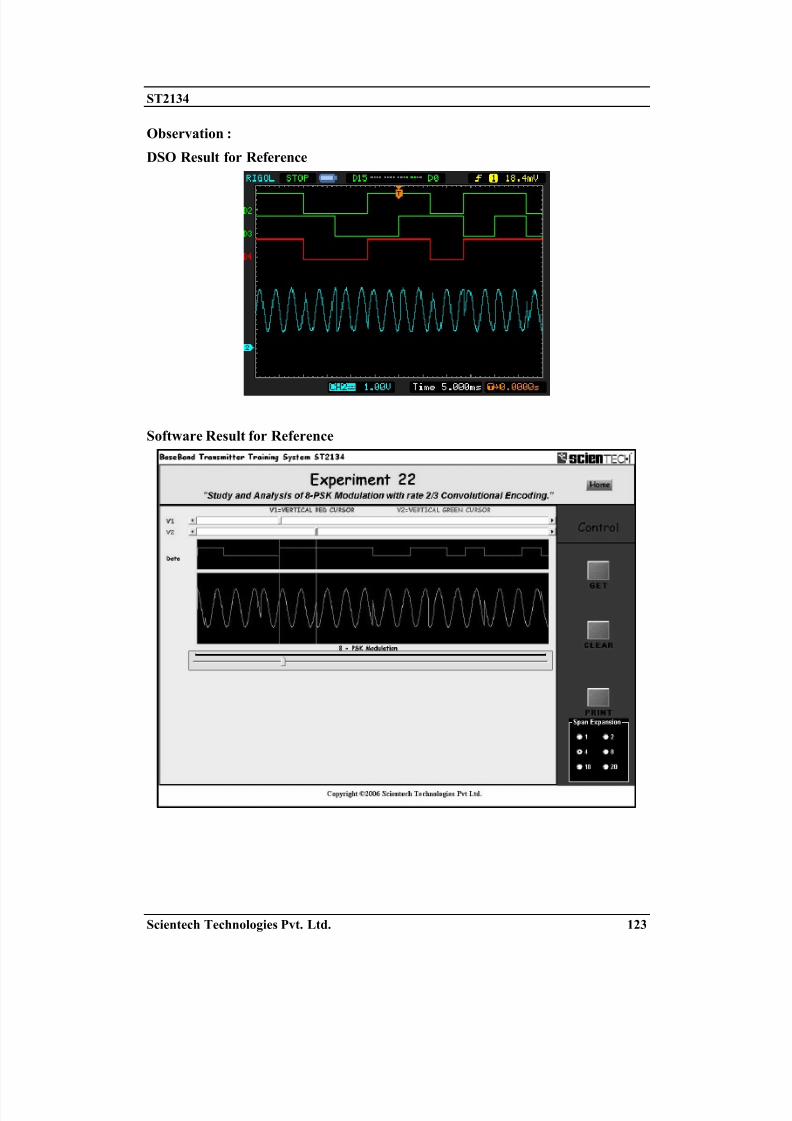
8/14/2019 ST2134 trainer kit manual
http://slidepdf.com/reader/full/st2134-trainer-kit-manual 123/171
ST2134
Scientech Technologies Pvt. Ltd. 123
Observation :
DSO Result for Reference
Software Result for Reference

8/14/2019 ST2134 trainer kit manual
http://slidepdf.com/reader/full/st2134-trainer-kit-manual 124/171
ST2134
Scientech Technologies Pvt. Ltd. 124
User Result :
Figure for Bit pattern
Figure for Symbol Pattern
Figure for I Channel Pattern
Figure for I Channel Modulation
Figure for Q Channel Pattern
Figure for Q Channel Modulation
Figure for 8PSK Modulation.
Result :

8/14/2019 ST2134 trainer kit manual
http://slidepdf.com/reader/full/st2134-trainer-kit-manual 125/171
ST2134
Scientech Technologies Pvt. Ltd. 125
Experiment 23
Objective :
Study, Analysis and Measurement of four bit encoding with pattern generator
and clock.Theory :
In four bit encoding techniques the incoming base band data stream is divided into
four data streams. Encoding is done in a manner that the rate of four new bit streams
will become 1/4 of that of the input baseband data.
Figure below shows the baseband data (0101110110001111100110100100) withrespect to clock and four encoded bits i.e BIT1, BIT2, BIT3, BIT4 having rates equals
to one fourth of the actual baseband data.
Procedure :
• Hardware Mode Steps
1. Switch ‘On’ Power Switch.
2. Set DIP D1, D2, D3, D4 to 0000.
3. Observe Clock frequency at test point TP2 with respect to Ground, it should
be 75Hz.
4. Set DIP D1, D2, D3, D4 to 0001, 0010, 0011, 0100, 0101, 0110, 0111 andobserve their respective frequencies at test point TP2.
5. Set Output Control i.e. D12, D13, D14, D15, D16 (10111)
6. Set pattern length by using DIP D7, D8 (00 – 64 bits, 01 – 32 bits, 10 – 16
bits, 11 – 8 bits) and observe corresponding bit pattern at Test Point TP3.
7. For above Pattern Length you can select pattern type using DIP D5, D6 (00 –
Type 1, 01 – Type2, 10 – Type3, 11 – Type 4)]
8. Observe 4 bit encoded data at test point TP19 (bit1), TP20 (bit2), TP21(bit3)
and TP22(bit4)
9. Observe the data rate of pattern at TP3 and rate of 4 bit encoded data at TP19,
TP20, TP21 and TP22 (4 bit Encoded data should be one fourth that oforiginal pattern).

8/14/2019 ST2134 trainer kit manual
http://slidepdf.com/reader/full/st2134-trainer-kit-manual 126/171
ST2134
Scientech Technologies Pvt. Ltd. 126
• Software Mode Steps
1. Switch ‘On’ Power Switch of ST2134.
2. For software mode Set DIP D1 to logic 1 (up position)
3. Open ST2134 software from start > ….
4. Use DIP D9 to select the set of Experiment i.e. experiment range to be
performed.
5. Click EXP23.
6. Set DIP D2, D3, D4 from 000 to 111.
7. Set pattern length by using DIP D7,D8 (00 – 64 bits, 01 – 32 bits, 10 – 16 bits,
11 – 8 bits) of ST2134
8. For above Pattern Length you can select pattern type using DIP D5, D6 (00 –
Type 1, 01 – Type2, 10 – Type3, 11 – Type 4)
9. Click GET button and observe the corresponding clock, pattern, 4 bit encoding
(bit1, bit2, bit3, bit4) on software window.
10. Use curser V1 and V2 for Analysis.
Observation :
DSO Result for Reference

8/14/2019 ST2134 trainer kit manual
http://slidepdf.com/reader/full/st2134-trainer-kit-manual 127/171
ST2134
Scientech Technologies Pvt. Ltd. 127
Software result for Reference
User Result (Hardware Mode) :
Clock
Pattern
Bit1
Bit2
Bit3
Bit4
Clock

8/14/2019 ST2134 trainer kit manual
http://slidepdf.com/reader/full/st2134-trainer-kit-manual 128/171

8/14/2019 ST2134 trainer kit manual
http://slidepdf.com/reader/full/st2134-trainer-kit-manual 129/171
ST2134
Scientech Technologies Pvt. Ltd. 129
Experiment 24
Objective :
Study, Analysis and Measurement of 16-PSK modulation with four bit encoding,
pattern generator and clock.Theory :
In four bit encoding techniques the incoming base band data stream is divided into
four data streams. Encoding was done in a manner that the rate of four new bit
streams will become 1/4 of that of the main baseband data.
Figure below shows the baseband data (01110110001111110) with respect to clockand four encoded bits i.e. BIT1, BIT2, BIT3 & BIT4 having rates equals to one -
fourth of the actual baseband data.
16-PSK :
In Experiment 19 we studied about 8 PSK modulations. We keep on subdividing the
signal space into smaller regions. Doing so one more time for 8-PSK so that each is
now only 22.5o apart, gives us 16 PSK. This will give 16 signals or symbol, so each
symbol can convey 4 bits. Bit rate is now four times that of BPSK for the samesymbol rate. The following figures show the 16-PSK signal at various stages during
modulation.

8/14/2019 ST2134 trainer kit manual
http://slidepdf.com/reader/full/st2134-trainer-kit-manual 130/171
ST2134
Scientech Technologies Pvt. Ltd. 130

8/14/2019 ST2134 trainer kit manual
http://slidepdf.com/reader/full/st2134-trainer-kit-manual 131/171
ST2134
Scientech Technologies Pvt. Ltd. 131
Procedure :
• Hardware Mode Steps
1. Switch ‘On’ Power Switch.
2. Set DIP D1, to 0 (down position) for Hardware mode
3. Set output control i.e. DIP D12,D13,D14,D15, D16 to (10111)
4. For clock frequency, Pattern length and pattern Type setting refer
Experiment 1.
5. Observe clock, Pattern, 4bit encoding (bit1, bit2, bit3, bit4), I ChannelModulation, Q Channel Modulation and 16PSK Modulation at respective test
points TP2, TP3, TP19, TP20, TP21, TP22, TP39, TP40 and TP41.
• Software Mode Steps
1. Switch ‘On’ Power Switch of ST2134.
2. For software mode Set DIP D1 to logic 1 (up position).
3. Open ST2134 software from start > ….
4. Use DIP D9 to select the set of Experiment i.e. experiment range to be
performed.
5. Click EXP24.
6. For clock frequency, Pattern length and pattern Type setting refer
Experiment 1.
7. Click GET button and observe the corresponding pattern and its corresponding
16PSK modulated waveform on software window.
8. Use curser V1 and V2 for Analysis.
Observation :
DSO Result for Reference

8/14/2019 ST2134 trainer kit manual
http://slidepdf.com/reader/full/st2134-trainer-kit-manual 132/171
ST2134
Scientech Technologies Pvt. Ltd. 132
Software Result for Reference

8/14/2019 ST2134 trainer kit manual
http://slidepdf.com/reader/full/st2134-trainer-kit-manual 133/171
ST2134
Scientech Technologies Pvt. Ltd. 133
User Result :
Figure for Bit pattern
Figure for Symbol Pattern
Figure for I Channel Pattern
Figure for I Channel Modulation
Figure for Q Channel Pattern
Figure for Q Channel Modulation
Figure for 16PSK Modulation.
Result :

8/14/2019 ST2134 trainer kit manual
http://slidepdf.com/reader/full/st2134-trainer-kit-manual 134/171
ST2134
Scientech Technologies Pvt. Ltd. 134
Experiment 25
Objective :
Study and Analysis of 16-PSK constellation
Theory :
16-PSK Constellation
In 16-PSK constellation there are 16 points on the circle with phase difference
of 22.5 deg. With this modulator 4 bits are processed to produce a single phase
change. This means that each symbol consists of 4 bits. The constellation for
this modulator scheme is shown below.

8/14/2019 ST2134 trainer kit manual
http://slidepdf.com/reader/full/st2134-trainer-kit-manual 135/171
ST2134
Scientech Technologies Pvt. Ltd. 135
Procedure :
• Hardware Mode Steps
1. Switch ‘On’ Power Switch.
2. Set DIP D1, to 0 (down position) for Hardware mode
3. Set output control i.e. DIP D12,D13,D14,D15, D16 to (11000)
4. For clock frequency, Pattern length and pattern Type setting refer
Experiment 1.
5. Set Oscilloscope in XY mode.
6. Connect BNC to Test Probe to channel 1, channel 2 and Observe Constellation
Pattern respectively at Test Point X6, Test Point Y6.
• Software Mode Steps
1. Switch ON Power Switch of ST2134.
2. For software mode Set DIP D1 to logic 1 (up position).
3. Open ST2134 software from start > ….
4. Use DIP D9 to select the set of Experiment i.e. experiment range to be performed.
5. Click EXP 25.
6. Click GET button and observe the corresponding Constellation Pattern of
16PSK.
Observation :
DSO Result for Reference

8/14/2019 ST2134 trainer kit manual
http://slidepdf.com/reader/full/st2134-trainer-kit-manual 136/171
ST2134
Scientech Technologies Pvt. Ltd. 136
Software Result for Reference
User Result (Hardware Mode) :
Result :

8/14/2019 ST2134 trainer kit manual
http://slidepdf.com/reader/full/st2134-trainer-kit-manual 137/171
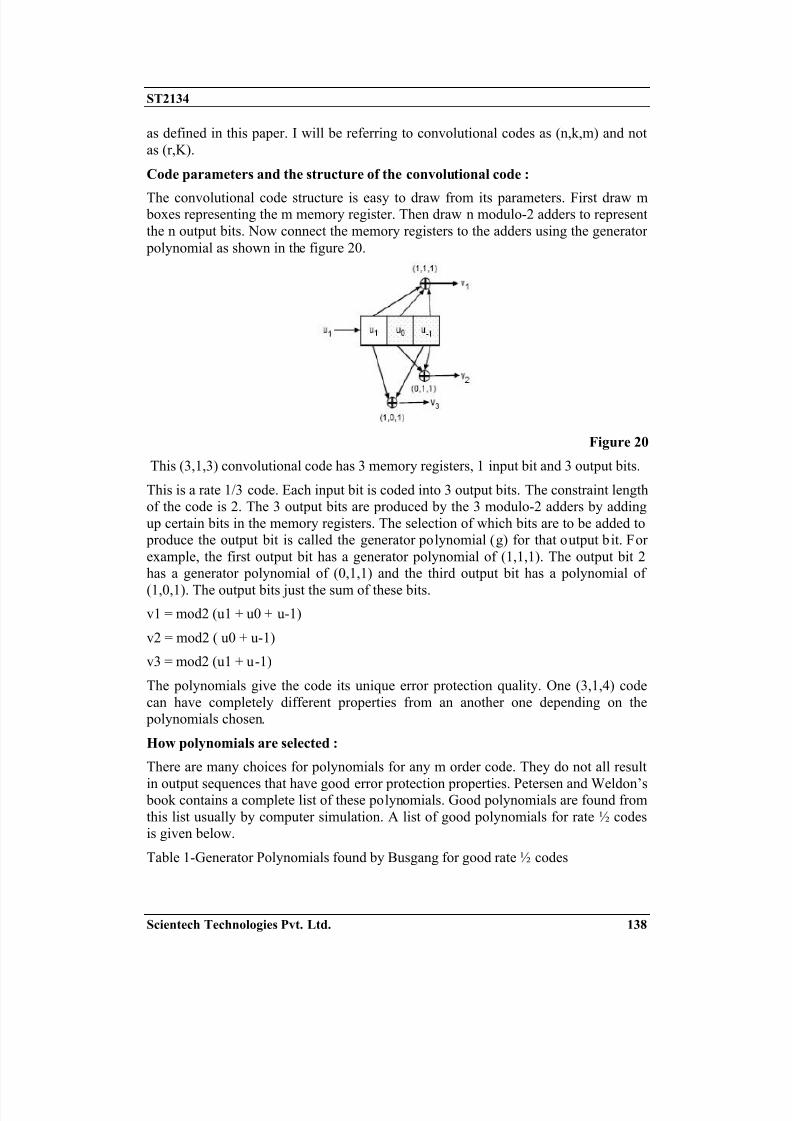
8/14/2019 ST2134 trainer kit manual
http://slidepdf.com/reader/full/st2134-trainer-kit-manual 138/171
ST2134
Scientech Technologies Pvt. Ltd. 138
as defined in this paper. I will be referring to convolutional codes as (n,k,m) and not
as (r,K).
Code parameters and the structure of the convolutional code :
The convolutional code structure is easy to draw from its parameters. First draw m boxes representing the m memory register. Then draw n modulo-2 adders to represent
the n output bits. Now connect the memory registers to the adders using the generator
polynomial as shown in the figure 20.
Figure 20
This (3,1,3) convolutional code has 3 memory registers, 1 input bit and 3 output bits.
This is a rate 1/3 code. Each input bit is coded into 3 output bits. The constraint length
of the code is 2. The 3 output bits are produced by the 3 modulo-2 adders by adding
up certain bits in the memory registers. The selection of which bits are to be added to
produce the output bit is called the generator polynomial (g) for that output bit. For
example, the first output bit has a generator polynomial of (1,1,1). The output bit 2
has a generator polynomial of (0,1,1) and the third output bit has a polynomial of
(1,0,1). The output bits just the sum of these bits.
v1 = mod2 (u1 + u0 + u-1)
v2 = mod2 ( u0 + u-1)
v3 = mod2 (u1 + u-1)
The polynomials give the code its unique error protection quality. One (3,1,4) code
can have completely different properties from an another one depending on the
polynomials chosen.
How polynomials are selected :
There are many choices for polynomials for any m order code. They do not all result
in output sequences that have good error protection properties. Petersen and Weldon’s book contains a complete list of these polynomials. Good polynomials are found from
this list usually by computer simulation. A list of good polynomials for rate ½ codes
is given below.
Table 1-Generator Polynomials found by Busgang for good rate ½ codes

8/14/2019 ST2134 trainer kit manual
http://slidepdf.com/reader/full/st2134-trainer-kit-manual 139/171
ST2134
Scientech Technologies Pvt. Ltd. 139
States of a code :
We have states of mind and so do encoders. We are depressed one day, and perhaps
happy the next from the many different states we can be in. Our output depends on
our states of mind and tongue in-cheek we can say that encoders too act this way.
What they output depends on what is their state of mind. Our states are complex butencoder states are just a sequence of bits. Sophisticated encoders have long constraint
lengths and simple ones have short in dicating the number of states they can be in.
The (2,1,4) code in figure 21 has a constraint length of 3. The shaded registers below
hold these bits. The unshaded register holds the incoming bit. This means that 3 bits
or 8 different combinations of these bits can be present in these memory registers.
These 8 different combinations determine what output we will get for v1 and v2, the
coded sequence.
The number of combinations of bits in the shaded registers are called the states of the
code and are defined by Number of states = 2L where L = the constraint length of the
code and is equal to L = k (m - 1).
Figure 21 The states of a code indicate what is in the memory registers
Think of states as sort of an initial condition. The output bit depends on this initial
condition, which changes at each time tick.
Let’s examine the states of the code (3, 2, 2) shown above. This code outputs 3 bitsfor every 2 input bit. It is a rate 2/3 code. Its constraint length is 2. The total number
of states is equal to 4. The eight states of this (3, 2, 2) code are: 00, 01, 10, 11 fordifferent combinations of 2 bit inputs

8/14/2019 ST2134 trainer kit manual
http://slidepdf.com/reader/full/st2134-trainer-kit-manual 140/171
ST2134
Scientech Technologies Pvt. Ltd. 140
State Table for Rate = 2/3
Input Bit Input states Output Bits Output states
Even
odd
SI1 SI2 V1 V2 V3 SO1 SO2
00 0 0 0 0 0 0 0
01 0 0 0 1 1 0 1
10 0 0 1 0 1 1 0
11 0 0 1 1 0 1 1
00 0 1 0 1 0 0 0
01 0 1 0 0 1 0 1
10 0 1 1 1 1 1 0
11 0 1 1 0 0 1 1
00 1 0 1 0 0 0 0
01 1 0 1 1 1 0 1
10 1 0 0 0 1 1 0
11 1 0 0 1 0 1 1
00 1 1 1 1 0 0 0
01 1 1 1 0 1 0 1
10 1 1 0 1 1 1 0
11 1 1 0 0 0 1 1
State machine used for 2/3 bit encoding is shown below
Consider a input bit stream 011110 and initial state is S0 i.e. 00

8/14/2019 ST2134 trainer kit manual
http://slidepdf.com/reader/full/st2134-trainer-kit-manual 141/171
ST2134
Scientech Technologies Pvt. Ltd. 141
The first information block is 01, causing the encoder to transit from S0 to S1 and
output coded word is 01
Now encoder is at state S1. The next information block is 11, causing the encoder to
transit from S1 to S3 and coded output word is 100.Similarly for the next information block 10, current state is S3, encoder causing state
change from S3 to S2 and output coded word is 011.
Procedure :
• Hardware Mode Steps
1. Switch ‘On’ Power Switch.
2. For hardware mode Set DIP D1 to logic 0 (Down position).
3. Set DIP D2, D3, D4 to 000.
4. Observe Clock frequency at test point TP2 with respect to Ground, it should be 18.75Hz.
5. Set DIP D1, D2, D3, D4 to 0001, 0010, 0011, 0100, 0101, 0110, 0111 andobserve their respective frequencies at test point TP2.
6. Set Output Control i.e. D12, D13, D14, D15, D16 (11001)
7. Set pattern length by using DIP D7, D8 (00 – 64 bits, 01 – 32 bits, 10 – 16
bits, 11 – 8 bits) and observe corresponding bit pattern at Test Point TP3.
8. For above Pattern Length you can select pattern type using DIP D5, D6 (00 –Type 1, 01 – Type2, 10 – Type3, 11 – Type 4)]
9. Observe Pattern out, 3 bit encoding, ¾ convolutional encoding at test point
TP3, TP13, TP14, TP15, TP23, TP24, TP25, TP26
• Software Mode Steps
1. Switch ON Power Switch of ST2134.
2. For software mode Set DIP D1 to logic 1 (up position).
3. Open ST2134 software from start > ….
4. Use DIP D9 to select the set of Experiment i.e. experiment range to be performed.
5. Click EXP26.
6. Set DIP D2,D3,D4 from 000 to 111 and set output control DIP D12, D13,
D14, D15, D16 to 11001.
7. Set pattern length by using DIP D7,D8 (00 – 64 bits, 01 – 32 bits, 10 – 16 bits,11 – 8 bits) of ST2134
8. For above Pattern Length you can select pattern type using DIP D5, D6 (00 –Type 1, 01 – Type2, 10 – Type3, 11 – Type 4)
9. Click GET button and observe the corresponding clock, pattern, 3 bit encoding(bit1, bit2, bit3), rate 3/4 convolutional encoding on software window.
10. Use curser V1 and V2 for Analysis.

8/14/2019 ST2134 trainer kit manual
http://slidepdf.com/reader/full/st2134-trainer-kit-manual 142/171
ST2134
Scientech Technologies Pvt. Ltd. 142
Observation :
DSO Result for Reference
Software result for Reference

8/14/2019 ST2134 trainer kit manual
http://slidepdf.com/reader/full/st2134-trainer-kit-manual 143/171
ST2134
Scientech Technologies Pvt. Ltd. 143
User Result (Hardware Mode) :
Clock
Pattern
Bit1
Bit2
Bit3
Bit1 of 3/4
Bit2 of 3/4
Bit3 of ¾
Bit4 of ¾
Clock
Pattern
Bit1
Bit2
Bit3
Bit1 of 3/4
Bit2 of 3/4

8/14/2019 ST2134 trainer kit manual
http://slidepdf.com/reader/full/st2134-trainer-kit-manual 144/171
ST2134
Scientech Technologies Pvt. Ltd. 144
Bit3 of ¾
Bit4 of ¾
Clock
Pattern
Bit1
Bit2
Bit3
Bit1 of 3/4
Bit2 of 3/4
Bit3 of ¾
Bit4 of ¾
Result :

8/14/2019 ST2134 trainer kit manual
http://slidepdf.com/reader/full/st2134-trainer-kit-manual 145/171
ST2134
Scientech Technologies Pvt. Ltd. 145
Experiment 27
Objective :
Study, Analysis and Measurement of 16 PSK modulation with rate 3/4
convolution encodingTheory :
3/4 rate convolutional encoded data is generated using the block diagram shown
below –
From the figure it is clear that pattern is first splitted in to 3 bit encoded data. Afterthat bit1 and bit2 is used as an input to the 2/3 rate convolutional encoder and bit 3 is
directly used as the fourth bit of ¾ rate convolutinal encoding.
Output rate of ¾ is same as that of 3bit encoder output.
Convolution Encoding-
Convolution codes are commonly specified by three parameters; (n,k,m).
n = number of output bits
k = number of input bits
m = number of memory registers
The quantity k/n called the code rate, is a measure of the efficiency of the code.
Commonly k and n parameters range from 1 to 8, m from 2 to 10 and the code ratefrom 1/8 to 7/8 except for deep space applications where code rates as low as 1/100 or
even longer have been employed.
Often the manufacturers of convolutional code chips specify the code by parameters
(n,k,L), The quantity L is called the constraint length of the code and is defined by
Constraint Length, L = k (m-1)

8/14/2019 ST2134 trainer kit manual
http://slidepdf.com/reader/full/st2134-trainer-kit-manual 146/171
ST2134
Scientech Technologies Pvt. Ltd. 146
The constraint length L represents the number of bits in the encoder memory that
affect the generation of the n output bits. The constraint length L is also referred to by
the capital letter K, which can be confusing with the lower case k, which represents
the number of input bits. In some books K is defined as equal to the product of k and
m. Often in commercial spec, the codes are specified by (r, K), where r = the code ratek/n and K is the constraint length. The constraint length K however is equal to L - 1,
as defined in this paper. I will be referring to convolutional codes as (n,k,m) and notas (r,K).
Code parameters and the structure of the convolutional code :
The convolutional code structure is easy to draw from its parameters. First draw m
boxes representing the m memory registers. Then draw n modulo-2 adders torepresent the n output bits. Now connect the memory registers to the adders using the
generator polynomial as shown in the figure 23.
Figure 23 This (3,1,3) convolutional code has 3 memory registers, 1 input bit and 3 output bits.
This is a rate 1/3 code. Each input bit is coded into 3 output bits. The constraint lengthof the code is 2. The 3 output bits are produced by the 3 modulo-2 adders by adding
up certain bits in the memory registers. The selection of which bits are to be added to produce the output bit is called the generator polynomial (g) for that output bit. For
example, the first output bit has a generator polynomial of (1,1,1). The output bit 2
has a generator polynomial of (0,1,1) and the third output bit has a polynomial of
(1,0,1). The output bits just the sum of these bits.
v1 = mod2 (u1 + u0 + u-1)
v2 = mod2 ( u0 + u-1)
v3 = mod2 (u1 + u-1)
The polynomials give the code its unique error protection quality. One (3,1,4) codecan have completely different properties from an another one depending on the
polynomials chosen.

8/14/2019 ST2134 trainer kit manual
http://slidepdf.com/reader/full/st2134-trainer-kit-manual 147/171
ST2134
Scientech Technologies Pvt. Ltd. 147
How polynomials are selected :
There are many choices for polynomials for any m order code. They do not all result
in output sequences that have good error protection properties. Petersen and Weldon’s
book contains a complete list of these polynomials. Good polynomials are found fromthis list usually by computer simulation. A list of good polynomials for rate ½ codes
is given below.
Table 1-Generator Polynomials found by Busgang for good rate ½ codes
States of a code :
We have states of mind and so do encoders. We are depressed one day, and perhaps
happy the next from the many different states we can be in. Our output depends onour states of mind and tongue in-cheek we can say that encoders too act this way.
What they output depends on what is their state of mind. Our states are complex but
encoder states are just a sequence of bits. Sophisticated encoders have long constraint
lengths and simple ones have short in dicating the number of states they can be in.
The (2,1,4) code in figure 24 has a constraint length of 3. The shaded registers below
hold these bits. The unshaded register holds the incoming bit. This means that 3 bitsor 8 different combinations of these bits can be present in these memory registers.
These 8 different combinations determine what output we will get for v1 and v2, thecoded sequence.
The number of combinations of bits in the shaded registers are called the states of the
code and are defined by Number of states = 2L where L = the constraint length of the
code and is equal to L = k (m - 1).
Figure 24

8/14/2019 ST2134 trainer kit manual
http://slidepdf.com/reader/full/st2134-trainer-kit-manual 148/171
ST2134
Scientech Technologies Pvt. Ltd. 148
The states of a code indicate what is in the memory registers
Think of states as sort of an initial condition. The output bit depends on this initial
condition which changes at each time tick.
Let’s examine the states of the code (3,2,2) shown above. This code outputs 3 bits forevery 2 input bit. It is a rate 2/3 code. Its constraint length is 2. The total number of
states is equal to 4. The eight states of this (3,2,2) code are: 00, 01, 10, 11 for different
combinations of 2 bit inputs
State Table for Rate = 2/3
Input Bit Input states Output Bits Output states
Even
odd
SI1 SI2 V1 V2 V3 SO1 SO2
00 0 0 0 0 0 0 0
01 0 0 0 1 1 0 1
10 0 0 1 0 1 1 011 0 0 1 1 0 1 1
00 0 1 0 1 0 0 0
01 0 1 0 0 1 0 1
10 0 1 1 1 1 1 0
11 0 1 1 0 0 1 1
00 1 0 1 0 0 0 0
01 1 0 1 1 1 0 1
10 1 0 0 0 1 1 0
11 1 0 0 1 0 1 1
00 1 1 1 1 0 0 001 1 1 1 0 1 0 1
10 1 1 0 1 1 1 0
11 1 1 0 0 0 1 1

8/14/2019 ST2134 trainer kit manual
http://slidepdf.com/reader/full/st2134-trainer-kit-manual 149/171
ST2134
Scientech Technologies Pvt. Ltd. 149
State machine used for 2/3 bit encoding is shown below
Consider a input bit stream 011110 and initial state is S0 i.e. 00The first information block is 01, causing the encoder to transit from S0 to S1 andoutput coded word is 01
Now encoder is at state S1. The next information block is 11, causing the encoder to
transit from S1 to S3 and coded output word is 100.
Similarly for the next information block 10, current state is S3, encoder causing state
change from S3 to S2 and output coded word is 011.
16-PSK :
In Experiment 19 we studied about 8 PSK modulations. We keep on subdividing the
signal space into smaller regions. Doing so one more time for 8-PSK so that each is
now only 22.5o apart, gives us 16 PSK. This will give 16 signals or symbol, so eachsymbol can convey 4 bits. Bit rate is now four times that of BPSK for the same
symbol rate. The following figures show the 16-PSK signal at various stages during
modulation.

8/14/2019 ST2134 trainer kit manual
http://slidepdf.com/reader/full/st2134-trainer-kit-manual 150/171
ST2134
Scientech Technologies Pvt. Ltd. 150

8/14/2019 ST2134 trainer kit manual
http://slidepdf.com/reader/full/st2134-trainer-kit-manual 151/171
ST2134
Scientech Technologies Pvt. Ltd. 151
Procedure :
• Hardware Mode Steps
1. Pattern Length you can select pattern type using DIP D5, D6 (00 – Type 1, 01
Switch ‘On’ Power Switch.
2. For hardware mode Set DIP D1 to logic 1 (up position).
3. Set DIP D2, D3, D4 to 000.
4. Observe Clock frequency at test point TP2 with respect to Ground, it should
be 75Hz.
5. Set DIP D1, D2, D3, D4 to 0001, 0010, 0011, 0100, 0101, 0110, 0111 and
observe their respective frequencies at test point TP2.
6. Set Output Control i.e. D12, D13, D14, D15, D16 (11010)
7. Set pattern length by using DIP D7, D8 (00 – 64 bits, 01 – 32 bits, 10 – 16
bits, 11 – 8 bits) and observe corresponding bit pattern at Test Point TP3.
8. For above – Type2, 10 – Type3, 11 – Type 4)]
9. Observe Pattern out, 3 bit encoding, ¾ convolutional encoding, Ichannen for
16 PSK, Q Channel for 16PSK, and 16PSK modulated signal at respective test
points TP3, TP13, TP14, TP15, TP23, TP24, TP25, TP26, TP39, TP40, and
TP41.
Observation :
DSO Result for Reference

8/14/2019 ST2134 trainer kit manual
http://slidepdf.com/reader/full/st2134-trainer-kit-manual 152/171
ST2134
Scientech Technologies Pvt. Ltd. 152
User Result (Hardware Mode) :
Clock
Pattern
I channel
multilevel
signal at X6
I channel
Modulated
Signal at
TP39
Q channel
multilevel
signal at Y6
Q channelModulated
Signal atTP40
16 PSK
ModulatedSignal at
TP41
Result :

8/14/2019 ST2134 trainer kit manual
http://slidepdf.com/reader/full/st2134-trainer-kit-manual 153/171
ST2134
Scientech Technologies Pvt. Ltd. 153
Experiment 28
Objective :
Study, Analysis, and measurement of 16 QAM Modulation with four bit
encoding.Theory :
16-QAM
In M-QAM, and this one is for M = 16, we vary not just the phase of the symbol butalso the amplitude. In PSK, all symbols sat on a circle so they all had the same
amplitude. Here the points closer to the axes have lesser amplitudes and hence energythan some others. We can compute the X and Y axis values of each of these points
and depending on the total power we want, we can set the value of a. For typicalconstellation, set a = 1. If we call the symbols integers then they range from 0 to 15.
We show a sequence of random integers up 15 in signal s1 below that we will usethese to create a 16QAM signal.
Symbol Bit Pattern Phase Magnitude
S1 0000 -135o 0.311 V
S2 0001 -165o 0.850 V
S3 0010 -45o 0.311 V
S4 0011 -15o 0.850 V
S5 0100 -105o 0.850 V
S6 0101 -135o 1.161V
S7 0110 -75o 0.850 V
S8 0111 -45o 1.161V
S9 1000 +135o 0.311 V
S10 1001 +165o 0.850 V
S11 1010 +45o 0.311 V
S12 1011 +15o 0.850 V
S13 1100 +105o 0.850 V
S14 1101 +135o 1.161V
S15 1110 +75o 0.850 V
S16 1111 +45o 1.161V
We can now multiply these signals with the cosine and the sine wave carriers. Then
add (or subtract) the two and you have the modulated carrier shown in s6.

8/14/2019 ST2134 trainer kit manual
http://slidepdf.com/reader/full/st2134-trainer-kit-manual 154/171
ST2134
Scientech Technologies Pvt. Ltd. 154
16-QAM Modulated Waveform

8/14/2019 ST2134 trainer kit manual
http://slidepdf.com/reader/full/st2134-trainer-kit-manual 155/171
ST2134
Scientech Technologies Pvt. Ltd. 155
Procedure :
• Hardware Mode Steps
1. Switch ‘On’ Power Switch.
2. Set DIP D1, to 0 (down position) for Hardware mode
3. Set output control i.e. DIP D12,D13,D14,D15, D16 to (11011)
4. For clock frequency, Pattern length and pattern Type setting refer
Experiment 1.
5. Observe clock, Pattern, 4bit encoding (bit1, bit2, bit3, bit4), I ChannelModulation, Q Channel Modulation and 16QAM Modulation at respective test
points TP2, TP3, TP19, TP20, TP21, TP22, TP39, TP40 and TP41.
• Software Mode Steps
1. Switch ‘On’ Power Switch of ST2134.
2. For software mode Set DIP D1 to logic 1 (up position).
3. Open ST2134 software from start > ….
4. Use DIP D9 to select the set of Experiment i.e. experiment range to be performed.
5. Click EXP28.
6. For clock frequency, Pattern length and pattern Type setting refer
Experiment 1.
7. Click GET button and observe the corresponding pattern and its corresponding
16QAM modulated waveform on software window.
8. Use curser V1 and V2 for Analysis.

8/14/2019 ST2134 trainer kit manual
http://slidepdf.com/reader/full/st2134-trainer-kit-manual 156/171
ST2134
Scientech Technologies Pvt. Ltd. 156
Observation :
DSO Result for Reference
Software Result for Reference

8/14/2019 ST2134 trainer kit manual
http://slidepdf.com/reader/full/st2134-trainer-kit-manual 157/171
ST2134
Scientech Technologies Pvt. Ltd. 157

8/14/2019 ST2134 trainer kit manual
http://slidepdf.com/reader/full/st2134-trainer-kit-manual 158/171
ST2134
Scientech Technologies Pvt. Ltd. 158
User Result :
Figure for Bit pattern
Figure for Symbol Pattern
Figure for I Channel Pattern
Figure for I Channel Modulation
Figure for Q Channel Pattern
Figure for Q Channel Modulation
Figure for 16QAM Modlation.
Result :

8/14/2019 ST2134 trainer kit manual
http://slidepdf.com/reader/full/st2134-trainer-kit-manual 159/171
ST2134
Scientech Technologies Pvt. Ltd. 159
Experiment 29
Objective :
Study and analysis of 16QAM Constellation
Theory :
16QAM Constellation

8/14/2019 ST2134 trainer kit manual
http://slidepdf.com/reader/full/st2134-trainer-kit-manual 160/171
ST2134
Scientech Technologies Pvt. Ltd. 160
Procedure :
• Hardware Mode Steps
1. Switch ‘On’ Power Switch.
2. Set DIP D1, to 0 (down position) for Hardware mode
3. Set output control i.e. DIP D12,D13,D14,D15, D16 to (11100)
4. For clock frequency, Pattern length and pattern Type setting refer
Experiment 1.
5. Set Oscilloscope in XY mode.
6. Connect BNC to Test Probe to channel 1, channel 2 and Observe Constellation
Pattern respectively at Test Point X7, Test Point Y7.
• Software Mode Steps
1. Switch ‘On’ Power Switch of ST2134.
2. For software mode Set DIP D1 to logic 1 (up position).
3. Open ST2134 software from start > ….
4. Use DIP D9 to select the set of Experiment i.e. experiment range to be performed.
5. Click EXP 29.
6. Click GET button and observe the corresponding Constellation Pattern of
16QAM.
Observation :DSO Result for Reference

8/14/2019 ST2134 trainer kit manual
http://slidepdf.com/reader/full/st2134-trainer-kit-manual 161/171
ST2134
Scientech Technologies Pvt. Ltd. 161
Software Result for Reference
User Result (Hardware Mode) :
Result :

8/14/2019 ST2134 trainer kit manual
http://slidepdf.com/reader/full/st2134-trainer-kit-manual 162/171
ST2134
Scientech Technologies Pvt. Ltd. 162
Experiment 30
Objective :
Study, Analysis and Measurement of 16 QAM modulation with rate 3/4
convolution encodingTheory :
3/4 rate convolutional encoded data is generated using the block diagram shown below :
From the figure it is clear that pattern is first splitted in to 3 bit encoded data. Afterthat bit1 and bit2 is used as an input to the 2/3 rate convolutional encoder and bit 3 is
directly used as the fourth bit of ¾ rate convolutinal encoding.
Output rate of ¾ is same as that of 3bit encoder output.
Convolution Encoding-
Convolution codes are commonly specified by three parameters; (n,k,m).
n = number of output bits
k = number of input bits
m = number of memory registers
The quantity k/n called the code rate, is a measure of the efficiency of the code.
Commonly k and n parameters range from 1 to 8, m from 2 to 10 and the code rate
from 1/8 to 7/8 except for deep space applications where code rates as low as 1/100 oreven longer have been employed.
Often the manufacturers of convolutional code chips specify the code by parameters(n,k,L), The quantity L is called the constraint length of the code and is defined by
Constraint Length, L = k (m-1)
The constraint length L represents the number of bits in the encoder memory that
affect the generation of the n output bits. The constraint length L is also referred to bythe capital letter K, which can be confusing with the lower case k, which represents
the number of input bits. In some books K is defined as equal to the product of k and
m. Often in commercial spec, the codes are specified by (r, K), where r = the code rate
k/n and K is the constraint length. The constraint length K however is equal to L - 1,
as defined in this paper. I will be referring to convolutional codes as (n,k,m) and not
as (r,K).

8/14/2019 ST2134 trainer kit manual
http://slidepdf.com/reader/full/st2134-trainer-kit-manual 163/171
ST2134
Scientech Technologies Pvt. Ltd. 163
Code parameters and the structure of the convolutional code :
The convolutional code structure is easy to draw from its parameters. First draw m
boxes representing the m memory registers. Then draw n modulo-2 adders to
represent the n output bits. Now connect the memory registers to the adders using thegenerator polynomial as shown in the figure 25.
Figure 25
This (3,1,3) convolutional code has 3 memory registers, 1 input bit and 3 output bits.
This is a rate 1/3 code. Each input bit is coded into 3 output bits. The constraint length
of the code is 2. The 3 output bits are produced by the 3 modulo-2 adders by adding
up certain bits in the memory registers. The selection of which bits are to be added to
produce the output bit is called the generator polynomial (g) for that output bit. For
example, the first output bit has a generator polynomial of (1,1,1). The output bit 2has a generator polynomial of (0,1,1) and the third output bit has a polynomial of
(1,0,1). The output bits just the sum of these bits.
v1 = mod2 (u1 + u0 + u-1)
v2 = mod2 ( u0 + u-1)
v3 = mod2 (u1 + u-1)
The polynomials give the code its unique error protection quality. One (3,1,4) codecan have completely different properties from an another one depending on the
polynomials chosen.
How polynomials are selected :
There are many choices for polynomials for any m order code. They do not all result
in output sequences that have good error protection properties. Petersen and Weldon’s
book contains a complete list of these polynomials. Good polynomials are found from
this list usually by computer simulation. A list of good polynomials for rate ½ codes
is given below.
Table 1-Generator Polynomials found by Busgang for good rate ½ codes
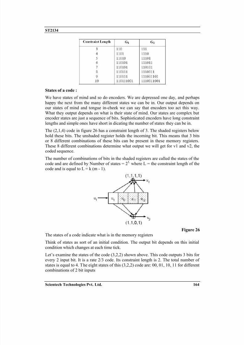
8/14/2019 ST2134 trainer kit manual
http://slidepdf.com/reader/full/st2134-trainer-kit-manual 164/171
ST2134
Scientech Technologies Pvt. Ltd. 164
States of a code :
We have states of mind and so do encoders. We are depressed one day, and perhaps
happy the next from the many different states we can be in. Our output depends onour states of mind and tongue in-cheek we can say that encoders too act this way.
What they output depends on what is their state of mind. Our states are complex butencoder states are just a sequence of bits. Sophisticated encoders have long constraint
lengths and simple ones have short in dicating the number of states they can be in.
The (2,1,4) code in figure 26 has a constraint length of 3. The shaded registers below
hold these bits. The unshaded register holds the incoming bit. This means that 3 bitsor 8 different combinations of these bits can be present in these memory registers.
These 8 different combinations determine what output we will get for v1 and v2, thecoded sequence.
The number of combinations of bits in the shaded registers are called the states of the
code and are defined by Number of states = 2L where L = the constraint length of the
code and is equal to L = k (m - 1).
Figure 26
The states of a code indicate what is in the memory registers
Think of states as sort of an initial condition. The output bit depends on this initialcondition which changes at each time tick.
Let’s examine the states of the code (3,2,2) shown above. This code outputs 3 bits for
every 2 input bit. It is a rate 2/3 code. Its constraint length is 2. The total number of
states is equal to 4. The eight states of this (3,2,2) code are: 00, 01, 10, 11 for different
combinations of 2 bit inputs

8/14/2019 ST2134 trainer kit manual
http://slidepdf.com/reader/full/st2134-trainer-kit-manual 165/171
ST2134
Scientech Technologies Pvt. Ltd. 165
State Table for Rate = 2/3
Input Bit Input states Output Bits Output states
Even
odd
SI1 SI2 V1 V2 V3 SO1 SO2
00 0 0 0 0 0 0 0
01 0 0 0 1 1 0 1
10 0 0 1 0 1 1 0
11 0 0 1 1 0 1 1
00 0 1 0 1 0 0 0
01 0 1 0 0 1 0 1
10 0 1 1 1 1 1 0
11 0 1 1 0 0 1 1
00 1 0 1 0 0 0 0
01 1 0 1 1 1 0 1
10 1 0 0 0 1 1 0
11 1 0 0 1 0 1 1
00 1 1 1 1 0 0 0
01 1 1 1 0 1 0 1
10 1 1 0 1 1 1 0
11 1 1 0 0 0 1 1
State machine used for 2/3 bit encoding is shown below
Consider a input bit stream 011110 and initial state is S0 i.e. 00

8/14/2019 ST2134 trainer kit manual
http://slidepdf.com/reader/full/st2134-trainer-kit-manual 166/171
ST2134
Scientech Technologies Pvt. Ltd. 166
The first information block is 01, causing the encoder to transit from S0 to S1 and
output coded word is 01
Now encoder is at state S1. The next information block is 11, causing the encoder to
transit from S1 to S3 and coded output word is 100.Similarly for the next information block 10, current state is S3, encoder causing state
change from S3 to S2 and output coded word is 011.
16QAM :
In M-QAM, and this one is for M = 16, we vary not just the phase of the symbol but
also the amplitude. In PSK, all symbols sat on a circle so they all had the sameamplitude. Here the points closer to the axes have lesser amplitudes and hence energy
than some others. We can compute the x and y axis values of each of these points anddepending on the total power we want, we can set the value of a. For typical
constellation, set a = 1. If we call the symbols integers then they range from 0 to 15.We show a sequence of random integers up 15 in signal s1 below that we will use
these to create a 16QAM signal.
Symbol Bit Pattern Phase Magnitude
S1 0000 -135o 0.311 V
S2 0001 -165o 0.850 V
S3 0010 -45o 0.311 V
S4 0011 -15o 0.850 V
S5 0100 -105o 0.850 V
S6 0101 -135o 1.161V
S7 0110 -75o 0.850 V
S8 0111 -45o 1.161V
S9 1000 +135o 0.311 V
S10 1001 +165o 0.850 V
S11 1010 +45o 0.311 V
S12 1011 +15o 0.850 V
S13 1100 +105o 0.850 V
S14 1101 +135o 1.161V
S15 1110 +75o 0.850 V
S16 1111 +45o 1.161V
We can now multiply these signals with the cosine and the sine wave carriers. Then
add (or subtract) the two and you have the modulated carrier shown in s6.

8/14/2019 ST2134 trainer kit manual
http://slidepdf.com/reader/full/st2134-trainer-kit-manual 167/171
ST2134
Scientech Technologies Pvt. Ltd. 167
16-QAM Modulated Waveform

8/14/2019 ST2134 trainer kit manual
http://slidepdf.com/reader/full/st2134-trainer-kit-manual 168/171
ST2134
Scientech Technologies Pvt. Ltd. 168
Procedure :
• Hardware Mode Steps
1. Switch ‘On’ Power Switch.
2. For hardware mode Set DIP D1 to logic 1 (up position).
3. Set DIP D2, D3, D4 to 000.
4. Observe Clock frequency at test point TP2 with respect to Ground, it should
be 75Hz.
5. Set DIP D1, D2, D3, D4 to 0001, 0010, 0011, 0100, 0101, 0110, 0111 andobserve their respective frequencies at test point TP2.
6. Set Output Control i.e. D12, D13, D14, D15, D16 (11101)
7. Set pattern length by using DIP D7, D8 (00 – 64 bits, 01 – 32 bits, 10 – 16
bits, 11 – 8 bits) and observe corresponding bit pattern at Test Point TP3.
8. For above Pattern Length you can select pattern type using DIP D5, D6 (00 –
Type 1, 01 – Type2, 10 – Type3, 11 – Type 4)]
9. Observe Pattern out, 3 bit encoding, ¾ convolutional encoding, Ichannen for
16 QAM, Q Channel for 16 QAM, and 16 QAM modulated signal at
respective test points TP3, TP13, TP14, TP15, TP23, TP24, TP25, TP26,
TP39, TP40, and TP41.
Observation :
DSO Result for Reference
User Result (Hardware Mode) :

8/14/2019 ST2134 trainer kit manual
http://slidepdf.com/reader/full/st2134-trainer-kit-manual 169/171
ST2134
Scientech Technologies Pvt. Ltd. 169
Clock
Pattern
I channel
multilevelsignal at X7
I channel
Modulated
Signal at
TP39
Q channel
multilevel
signal at Y7
Q channel
Modulated
Signal atTP40
16 QAM
ModulatedSignal at
TP41
Result :
8/14/2019 ST2134 trainer kit manual
http://slidepdf.com/reader/full/st2134-trainer-kit-manual 170/171
ST2134
Scientech Technologies Pvt. Ltd. 170
FAQ’s
1. What do you mean by real-time software?
Ans.: Real-time software is software with the help of which student can configurethe hardware for respective experiment & acquire, visualize the real-time
selected signal for study.
2. What do you mean by simulation software?
Ans.: Simulation software is a software with the help of which student can study the
encoding & modulation technique without hardware.
3. What should be the mode setting for parallel port interface?
Ans.: Mode setting for parallel port interface should be Standard Port Type, this you
can set in BIOS setting of a computer.
4. What is the use of external reset?Ans.: With the help of external reset student can reset the complete hardware. Press
reset for new experiment.
5. What do you mean by output pattern type-length?
Ans.: Inbuilt Pattern Generator of variable pattern length and pattern type is provided.
Out of 4 DIP switches.D5 & D6 can be used to change the type of pattern for selected pattern length.
D7 & D8 can be used to change the pattern length.
6. What is the use of Experiment range select?
Ans.: This DIP switch can be used to select the set of experiments in real-timesoftware mode.
Set 1: Experiment 1 to 16
Set 2: Experiment 17 to 30
7. What is the role of external trigger out?
Ans.: Trigger out will help to trigger the Oscilloscope in the external mode.
With the help of trigger out EYE pattern can easily observed.

8/14/2019 ST2134 trainer kit manual
http://slidepdf.com/reader/full/st2134-trainer-kit-manual 171/171
ST2134
Warranty
1) We guarantee the product against all manufacturing defects for 24 months from
the date of sale by us or through our dealers. Consumables like dry cell etc. are
not covered under warranty.2) The guarantee will become void, if
a) The product is not operated as per the instruction given in the operating
manual.
b) The agreed payment terms and other conditions of sale are not followed.
c) The customer resells the instrument to another party.
d) Any attempt is made to service and modify the instrument.
3) The non-working of the product is to be communicated to us immediately giving
full details of the complaints and defects noticed specifically mentioning the
type, serial number of the product and date of purchase etc.
4) The repair work will be carried out, provided the product is dispatched securely
packed and insured. The transportation charges shall be borne by the customer.
Related Documents