72 SPRING 2012 IEEE SOLID-STATE CIRCUITS MAGAZINE A SSCS-Utah Chapter Kickoff Meeting DLs Kofi Makinwa and Un-Ku Moon Speak An inaugural conference to celebrate the birth of SSCS-Utah took place at the University of Utah in Salt Lake City on 24 February 2012, with twin presentations by SSCS Distinguished Lecturers Un-Ku Moon and Kofi Makinwa. Sponsored by Mentor Graph- ics and cosponsored by National Instruments and Electro Rent, the king-sized event was attended by engineers, students, and profes- sors from Cirque Corporation, ON Semiconductor, Crest Semiconduc- tor, Intel, Utah State University, and the University of Utah. It included a Chapter planning meeting at the end to collect feedback and ideas from SSCS members. Established officially by the IEEE Membership and Geographic Activi- ties Department in November 2011, SSCS-Utah aims to provide an avenue for local IC designers to gather, share knowledge, and take advantage of the excel- lent benefits offered to SSCS members. Additionally, SSCS- Utah aims to create a bridge between local industry and academia in the hope of encouraging more students to study IC design. SSCS-Utah is centered in Salt Lake City, where IC interests include instru- mentation and communications circuits, amplifiers, and medium- to high-speed data converters. The idea and start-up efforts for the group began with several analog IC design- ers from Cirque Corpo- ration in Salt Lake City, Utah. Dave Willis and Brent Quist conceived the idea, while Steve Noall gathered the nec- essary signatures from local IC designers, uni- versity professors, and students. Willis, Quist, and Noall are now chair, vice-chair, and secretary, respectively. —Steve Noall SSCS DLs Kofi Makinwa (in front, third from left) and Un-Ku Moon (front row, second from right) headlined the inaugural meeting of SSCS-Utah in February. Digital Ob ject Id entifier 10.1109/MSSC .2012.2191900 Date of publication: 13 June 2012 SSCS-Utah aims to provide an avenue for local IC designers to gather, share knowledge, and take advantage of the excellent benefits offered to SSCS members.

Welcome message from author
This document is posted to help you gain knowledge. Please leave a comment to let me know what you think about it! Share it to your friends and learn new things together.
Transcript

72 SPRING 20 12 IEEE SOLID-STATE CIRCUITS MAGAZINE
A
SSCS-Utah Chapter Kickoff MeetingDLs Kofi Makinwa and Un-Ku Moon Speak
An inaugural conference to celebrate
the birth of SSCS-Utah took place at
the University of Utah in Salt Lake
City on 24 February 2012, with twin
presentations by SSCS Distinguished
Lecturers Un-Ku Moon and Kofi
Makinwa.
Sponsored by Mentor Graph-
ics and cosponsored by National
Instruments and Electro Rent, the
king-sized event was attended by
engineers, students, and profes-
sors from Cirque Corporation, ON
Semiconductor, Crest Semiconduc-
tor, Intel, Utah State University, and
the University of Utah. It included a
Chapter planning meeting at the end
to collect feedback and ideas from
SSCS members.
Established officially by the IEEE
Membership and Geographic Activi-
ties Department in November 2011,
SSCS-Utah aims to provide
an avenue for local IC
designers to gather, share
knowledge, and take
advantage of the excel-
lent benefits offered
to SSCS members.
Additionally, SSCS-
Utah aims to create
a bridge between
local industry and
academia in the
hope of encouraging
more students to study IC design.
SSCS-Utah is centered in Salt Lake
City, where IC interests include instru-
mentation and communications
circuits, amplifiers, and medium-
to high-speed data converters. The
idea and start-up efforts for the group
began with several analog IC design-
ers from Cirque Corpo-
ration in Salt Lake City,
Utah. Dave Willis and
Brent Quist conceived
the idea, while Steve
Noall gathered the nec-
essary signatures from
local IC designers, uni-
versity professors, and
students. Willis, Quist,
and Noall are now chair,
vice-chair, and secretary,
respectively.
—Steve Noall
SSCS DLs Kofi Makinwa (in front, third from left) and Un-Ku Moon (front row, second from right) headlined the inaugural meeting of SSCS-Utah in February.
Digital Ob ject Id entifier 10.1109/MSSC .2012.2191900
Date of publication: 13 June 2012
SSCS-Utah aims to provide an avenue for local IC designers to gather, share knowledge, and take advantage of the excellent benefi ts offered to SSCS members.

IEEE SOLID-STATE CIRCUITS MAGAZINE SPRING 20 12 73
In this lecture, Dr. Makinwa described the use of chopping and auto zeroing to design low-offset circuits in standard CMOS processes. Such dynamic error correction techniques are increasingly used to combat the increased variabil-ity and 1/f noise associated with modern CMOS processes.
Being a sampled-data technique, the use of auto zeroing usually incurs a certain noise penalty due to the aliasing of wide-band noise (Figure 1). In contrast, the use of chopping results in significantly less noise, but requires more complex circuitry to sup-press the “chopper ripple” caused by up-modulated offset and 1/f noise (Figure 2).
The above-mentioned techniques can be combined to good effect, such as by the use of auto zeroing and chopping [1] or by the use of nested chopping [2]. In recent years, power-efficient chopper amplifiers have used switched-capacitor filters [3] or ripple-reduction loops [4] to efficiently suppress chopper ripple (Figures 3 and 4).
References[1] A. T. K. Tang, “A 3nV-offset operational amplifier
with 20nV/ :Hz input noise PSD at DC employ-ing both chopping and autozeroing,” in Digest ISSCC, p. 386–387, Feb. 2002.
[2] A. Bakker, K. Thiele, and J. H. Huijsing, “A CMOS nested chopper instrumentation amplifier with 100nV offset,” J. Solid-State Circuits, vol. 35, no. 12, pp. 1877–1883, Dec. 2000.
[3] R. Burt and J. Zhang, “A micropower chopper-stabilized operational amplifier using a SC notch filter with synchronous integration inside the
FIGURE 1: Auto zeroing aliases noise into the baseband.
Vin+–
–+
M1 (Ron = 3k) Vout
Vclock
10 pF
100 kHz
Courtesy of R. Burt, TI
50n
40n
30n
20n
10n
V/s
qrt (
Hz)
100 1K 10K 100K 1M 10M 100MFrequency (Hz)
Noise Spectrumwith M1 Turned On
Sampled Noise Spectrum
PSSAnalysis
Residual Noise of Auto Zeroing
• S and H with 100-kHz clock and 50% duty cycle.
• Notches at multiples of 2fclock due to 50% duty cycle.
• Noise aliasing ⇒ Factor of six increase in LF noise.
• Sampled noise spectrum obtained with Spectre RF.
FIGURE 2: Chopping requires adding a filter.
Vch
Vin VoutVos
SignalOffset
0
LPF
Modulated Offset ⇒ Chopping Ripple• Can be removed by a low-pass filter.• But analog filters with low cut-off frequencies are difficult to realize on chip.
Chopper Ripple
Vin
Vch
VoutGm
Sampling Instants
S and H
Switched Capacitor Filter
e
[2]
• Chopped offset is integrated and the triangular ripple is then sampled at the zero crossings.• SC filter essentially eliminates residual ripple.• Filter introduces delay and a (small) noise penalty.
FIGURE 3: Switched capacitor filter to suppress ripple.
ABSTRACT: DYNAMIC OFFSET COMPENSATION TECHNIQUES IN CMOS

74 SPRING 20 12 IEEE SOLID-STATE CIRCUITS MAGAZINE
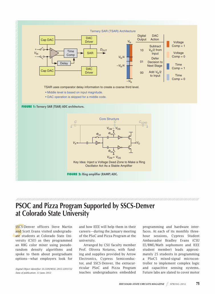
In this lecture, Dr. Moon discussed emerging anolog-digital-converter (ADC) architectures that attempt to enhance performance by exploiting the time domain. Examples include comparator-based ADCs [1], [2], VCO-based ADCs [3], [4], the ternary SAR (TSAR) ADC [5], and the ring-amplifier-based ADC [6].
One of the latest ideas is the TSAR ADC [5], which uses the delay of a dynamic comparator to attain another quantization level for each comparison, leading to three levels from two (Figure 1). This delay is inversely proportional to the magnitude of the input voltage. If the volt-age comparator does not decide fast enough, the time comparator (a digital latch) detects this extended delay and resolves it as the third level, corresponding to the input signal in the middle region closer to comparator threshold. Faster comparator decision is ordinarily used as the high and low levels. The combined information results in a three-level quantization.
Another new architecture, shown in Figure 2, converts a ring os-cillator into a ring amplifier (RAMP) by introducing a stabilizing volt-age “dead zone” into an output stage [6]. Because this architecture is based on simple inverters, it is extremely power efficient, requires
no bias currents, and readily scales. A performance greater than 12 ENOB and 45 fJ/step set a new milestone in the Murmann charts [7].
References[1] T. Sepke, J. K. Fiorenza, C. G. Sodini, P. Holloway, and H.-S. Lee, “Comparator-
based switched-capacitor circuits for scaled CMOS technologies,” in Proc. IEEE Int. Solid-State Circuits Conf., Dig. Technical Papers, ISSCC 2006, Feb. 6–9, 2006, pp. 812–821.
[2] L. Brooks and H.-S. Lee, “A 12b 50MS/s fully differential zero-crossingbased ADC without CMFB,” in Proc. IEEE Int. Solid-State Circuits Conf. Dig. Technical Papers, ISSCC 2009, Feb. 8–12, 2009, pp. 166 –167, 167a.
[3] M. Z. Straayer and M. H. Perrott, “A 10-bit 20 MHz 38 mW 950 MHz CT R∆ADC with a 5-bit noise-shaping VCO-based quantizer and DEM circuit in 0.13u CMOS,” in Proc. IEEE Symp. VLSI Circuits, June 14–16, 2007, pp. 246–247.
[4] K. Reddy, S. Rao, R. Inti, B. Young, A. Elshazly, M. Talegaonkar, and P. K. Hanumolu, “A 16 mW 87 dB-SNDR 10 MHz-BW CT-SD ADC using residue-canceling VCO-based quantizer,” in Proc. IEEE Int. Solid-State Circuits Conf. Dig. Technical Papers, ISSCC 2012, Feb. 19–23, 2012, pp. 152–153.
[5] J. Guerber, M. Gande, H. Venkatram, A. Waters, and U.-K. Moon, “A 10b ter-nary SAR ADC with decision time quantization based redundancy,” in Proc. IEEE Asian Solid State Circuits Conf. (A-SSCC), Nov. 14–16, 2011, pp. 65–68.
[6] B. Hershberg, S. Weaver, K. Sobue, S. Takeuchi, K. Hamashita, and U.-K. Moon, “Ring amplifieres for switched-capacitor circuits,” in Proc. IEEE Int. Solid-State Cir-cuits Conf. Dig. Technical Papers, ISSCC 2012, Feb. 19–23, 2012, pp. 460–461.
[7] Available: http://www.stanford.edu/~murmann/adcsurvey.html
—David J. Willis
FIGURE 4: Ripple-reduction loop.
f1 f1
f1
f2 f2Offset: dc
Ripple: ac
Signal: dc
VinVos
CH1 CH3
CH6
CH4 CH5
Gm3 Gm2Gm1
Gm6Gm5
Cint
C2
C1
Vout, Ripple
R1
Vfbk
C4
Vint IDC IAC
Signal: dc
See R. Wu, JSSC 2009 [4].
• Demodulate output ripple ⇒ Indirectly measure Vos.
• Then compensate for it.
• Narrow notch does not significantly affect stability.
R2 = C dVdt
IT’S ABOUT TIME! (MAKING BEST USE OF INFORMATION IN TIME)
continuous-time signal path,” J. Solid-State Circuits, vol. 41, no. 12, pp. 2729–2736, Dec. 2006.
[4] R. Wu, K. A. A. Makinwa, and J. H. Huijsing, “A chopper current-feedback instrumentation amplifier with a 1mHz 1/f noise corner and an AC-coupled
ripple reduction loop,” J. Solid-State Circuits, vol. 44, no. 12, pp. 3232–3243, Dec. 2009.
—Kofi Makinwa
IEEE SOLID-STATE CIRCUITS MAGAZINE SPRING 20 12 75
SSSCS-Denver officers Steve Martin
and Scott Evans visited undergradu-
ate students at Colorado State Uni-
versity (CSU) as they programmed
an RBG color mixer using pseudo-
random density algorithms and
spoke to them about postgraduate
options—what employers look for
and how IEEE will help them in their
careers—during the January meeting
of the PSoC and Pizza Program at the
university.
Arranged by CSU faculty member
Prof. Olivera Notaros, with fund-
ing and supplies provided by Arrow
Electronics, Cypress Semiconduc-
tor, and SSCS-Denver, the extracur-
ricular PSoC and Pizza Program
teaches undergraduates embedded
programming and hardware inter-
faces. At each of its monthly three-
hour sessions, Cypress Student
Ambassador Bradley Evans (CSU
EE/BME/Math sophomore and IEEE
student member) leads approxi-
mately 25 students in programming
a PSoC5 mixed-signal microcon-
troller to implement complex logic
and capacitive sensing systems.
Future labs are slated to cover motor
Core Structure
VO
ΦrstΦrst
Φrst
VX
CC CLOAD
VCM – VOS
VCM + VOS
Key Idea: Inject a Voltage Dead Zone to Make a RingOscillator Act As a Stable Amplifier
FIGURE 2: Ring amplifier (RAMP) ADC.
PSOC and Pizza Program Supported by SSCS-Denver at Colorado State University
Digital Ob ject Id entifier 10.1109/MSSC .2012.2203722
Date of publication: 13 June 2012
FIGURE 1: Ternary SAR (TSAR) ADC architecture.
TSAR uses comparator delay information to create a coarse third level.
• Middle level is based on input magnitude.
• DAC operation is skipped for a middle code.
Vfs/4
Vfs
–Vfs/4
–Vfs
10
01
00
SubtractVfs/2 from
Input
Add Vfs/2to Input
DeferDecision toNext Stage
DigitalOutput
DACAction
VoltageComp = 1
VoltageComp = 0
TimeComp = 1
TimeComp = 0
SAR
DACDriver
DACDriver
Cap DAC
VIN
DOUTTimeComp
Delay
Ternary SAR (TSAR) Architecture
+ +
– –
Cap DAC
Related Documents