SSCG METHODS OF EMI EMISSIONS REDUCTION APPLIED TO SWITCHING POWER CONVERTERS A thesis presented by José Alfonso Santolaria Lorenzo to The Department of Electronics Engineering in partial fulfillment of the requirements for the degree of Doctor of Philosophy in the subject of Electronic Engineering This thesis was directed by Ph.D. Josep Balcells i Sendra UNIVERSITAT POLITÈCNICA DE CATALUNYA June, 2004

Welcome message from author
This document is posted to help you gain knowledge. Please leave a comment to let me know what you think about it! Share it to your friends and learn new things together.
Transcript
SSCG METHODS OF EMI EMISSIONS REDUCTION APPLIED
TO SWITCHING POWER CONVERTERS
A thesis presented by
José Alfonso Santolaria Lorenzo
to
The Department of Electronics Engineering
in partial fulfillment of the requirements for the
degree of Doctor of Philosophy in the subject of
Electronic Engineering
This thesis was directed by
Ph.D. Josep Balcells i Sendra
UNIVERSITAT POLITÈCNICA DE CATALUNYA
June, 2004


ACKNOWLEDGEMENTS
Every task in our life is the sum of our own effort and the help and support of people
around us. I'm sure both things share the same weight in the final result. For this
reason, it's a pleasure for me to express my gratitude to all people without whom, I
couldn't have finished successfully one of the most important periods of my life:
To my family, my wonderful family: my father José, my mother Concha, my sister
MariCarmen, my brother-in-law Antonio and my niece María. There are no enough
words to express my gratitude for the whole support received during all these years,
but nothing would have been possible without them. Thanks again.
I must extend both my thanks and admiration to my thesis director, Josep Balcells. He
was the wise sailor who knew to fix the navigation course in those moments of storm
to, finally, reach a successful port.
I'm particularly grateful to David González and Javier Gago for the time dedicated to
read my papers and the thesis itself and give me their valuable comments.
Lastly my thanks go to David Saltiveri for helping me with PSPICE simulations and the
construction of the hardware prototype. He is the kind of people who only need few
words to understand what you want, what is very worthy when you don't have time.
If I forget mentioning any persons who also gave me their help and support, from
here, I express my excuses and I hope they don't take this mistake into consideration.
Thanks.
June, 2004 A.D.

INDEX
i
INDEX OF CONTENTS
1. INTRODUCTION.................................................................................................3
1.1 Objectives of this thesis .................................................................................3
1.2 Motivation ....................................................................................................3
1.3 State of Art...................................................................................................7
1.4 Generic structure of the thesis ..................................................................... 13
1.5 Experimental considerations and operative guideline...................................... 14
2. THEORETICAL BASIS........................................................................................ 19
2.1 Modulation ................................................................................................. 19
2.1.1 Frequency Modulation (FM) ................................................................... 21
2.1.1.1 Generic Formulation of Frequency Modulation ................................... 21
2.1.1.2 Other important parameters ............................................................ 23
2.1.1.2.1 Modulation ratio δ ..................................................................... 23
2.1.1.2.2 Modulation profiles.................................................................... 23
2.1.2 Bandwidth of the FM waveform.............................................................. 25
2.1.3 Sinusoidal carrier vs. a generic carrier: validity of modulation results ......... 25
2.1.3.1 Spectral content of a signal [RD-3] & [RD-8] ..................................... 26
2.1.3.2 Impact of modulation on every spectral component ........................... 28
2.2 Practical considerations related to FM parameters .......................................... 30
2.2.1 Carrier (Switching) & modulating frequencies .......................................... 30
2.2.2 Carrier frequency peak deviation ∆fc (Overlap) ........................................ 32
2.2.3 Influence of the modulation profile parameters........................................ 35
2.2.3.1 Influence on the power converter output voltage of the modulation
profile ....................................................................................................... 35
INDEX
ii
2.2.3.2 Influence on the final spectrum of a voltage offset in the modulation
profile....................................................................................................... 37
2.2.3.3 Influence of the modulation profile phase-shift on the spectrum resulting
from the modulation process ...................................................................... 40
2.2.3.4 Influence of the frequency peak deviation ∆fc defined by the modulation
profile....................................................................................................... 41
2.2.3.5 Influence of a modulation profile with a certain average value ........... 44
2.3 Computation of Frequency Modulation (SSCG) by means of a MATLAB algorithm
...................................................................................................................... 47
2.3.1 Considerations to apply FFT correctly to the MATLAB algorithm................ 47
2.3.2 Mathematical formulation of FM applied to different modulation profiles.... 51
2.3.2.1 Sinusoidal modulation profile........................................................... 52
2.3.2.2 Triangular modulation profile........................................................... 54
2.3.2.3 Exponential modulation profile......................................................... 56
2.3.2.4 Discrete modulation profile.............................................................. 60
2.3.3 Structure of the algorithm ..................................................................... 64
2.3.4 The MATLAB algorithm code lines .......................................................... 66
2.3.5 Verification of the algorithm .................................................................. 66
2.4 Summary................................................................................................... 75
3. THEORETICAL ANALYSIS OF EMI WITH DIFFERENT MODULATION PARAMETERS 81
3.1 Sinusoidal modulation profile ....................................................................... 83
3.1.1 Evolution of the central harmonic amplitude F1 ....................................... 89
3.1.2 Evolution of the maximum envelope amplitude Fenv,peak ............................ 92
3.1.3 Evolution of the peak-to-peak envelope bandwidth ∆fpeak ......................... 96
3.2 Triangular modulation profile....................................................................... 99
3.2.1 Dependence on the modulation index....................................................102
3.2.2 Evolution of the central harmonic amplitude F1 ......................................104
INDEX
iii
3.2.3 Evolution of the maximum envelope amplitude Fenv,peak ........................... 106
3.2.4 Evolution of the peak-to-peak envelope bandwidth ∆fpeak........................ 110
3.3 Exponential modulation profile ................................................................... 113
3.3.1 Dependence on the modulation index ................................................... 115
3.3.2 Evolution of the central harmonic amplitude F1 ...................................... 118
3.3.3 Evolution of the maximum envelope amplitude Fenv,peak ........................... 120
3.3.4 Evolution of the peak-to-peak envelope bandwidth ∆fpeak........................ 124
3.4 Comparison of the different modulation profiles........................................... 126
3.4.1 Considerations to the complete spectral content of a signal .................... 128
3.4.2 Considerations to the spectra distribution shape .................................... 130
3.5 Proposal of control for a real power converter ............................................. 134
3.6 Considerations to apply a certain SSCG method to switching power converters
..................................................................................................................... 136
3.7 Summary ................................................................................................. 137
4. APPLICATION OF SSCG TO EMI EMISSIONS REDUCTION IN SWITCHING POWER
CONVERTERS .................................................................................................... 145
4.1 Description of the test plant....................................................................... 148
4.1.1 Power conversion stage (UNIT 1) ......................................................... 151
4.1.2 Frequency modulation generator (UNIT 2) ............................................ 168
4.1.3 Physical implementation ...................................................................... 179
4.2 Influence of the Spectrum Analyzer's RBW .................................................. 183
4.3 Proposal of a practical method to select a valuable SSCG technique applied to
Switching Power Converters ............................................................................ 191
4.4 Comparative measurements of conducted EMI within the range of conducted
emissions (0 Hz ÷ 30 MHz) [RB-3].................................................................... 196
4.5 SSCG as a method to avoid interfering a certain signal................................. 200
4.6 Summary ................................................................................................. 207
INDEX
iv
5. CONCLUSIONS ...............................................................................................213
5.1 Further lines of investigations .....................................................................220
6. REFERENCES..................................................................................................225
GLOSSARY OF TERMS.........................................................................................233
ANNEXES: ANNEX 1. SPECTRUM ANALYZERS: PRACTICAL CONSIDERATIONS......................... A-3
ANNEX 2. NORMATIVE REQUIREMENTS TO MEASURE EMI.................................. A-19
ANNEX 3. CONCEPTS OF FOURIER TRANSFORM................................................. A-27
ANNEX 4. MATLAB ALGORITH CODE LINES ........................................................ A-41
ANNEX 5. CONSIDERATIONS ABOUT EMC UNITS EXPRESSED IN DECIBELS.......... A-49
ANNEX 6. SCHEMATICS AND PCBs CORRESPONDING TO THE TEST PLANT .......... A-55
ANNEX 7. PSPICE SIMULATION OF THE TEST PROTOTYPE.................................. A-61

C H A P T E R
1
INTRODUCTION

INTRODUCTION
3
1. INTRODUCTION
1.1 Objectives of this thesis
Spread Spectrum Clock Generation (SSCG) techniques have been studied and
implemented in digital systems ([RA-2] to [RA-6]), where a clock signal is normally one
of the main sources of EMI emissions. Clock-related signals (port lines, serial
communications and so on) are also an indirect way of emission of EMI. Although the
presence of SSCG-techniques in digital systems is not a strange situation in some
specific commercial applications, it is nearly unknown in the world of switching power
converters. The main objective of this thesis deals with the worthy possibility of
implementing such techniques in switching power converters in order to reduce EMI
emissions due to the PWM signal controlling these converters.
Besides, it is very difficult to find bibliography directly related to SSCG and, when
found, terms nearer to "feeling", "approximately", "rule of thumb" than to
mathematical expressions are the commonest. It would be worthy to have these SSCG-
techniques analytically expressed and systematized: this is another important objective
of this thesis.
Finally, SSCG-techniques offer the capability of moving the modulation spectrum as
desired (of course, with certain limitations); this fact can be profitable in order to avoid
undesired interferences with other systems and will be studied in this thesis.
1.2 Motivation
Many methods for EMI suppression have been developed in the last fifty years, most of
them, showing a hardly change in its implementation.
Traditional tools for EMI suppression are related to the use of filters, shielding
techniques and new methods for layout improvement. A complete set or rules have
been growing around these techniques just to take most profit of them when trying to
reduce EMI emissions:
INTRODUCTION
4
• Frequency and bandwidth of both signals used in a unit and their harmonics
must be limited to the absolutely necessary minimum.
• Frequencies and their harmonics should differ from those reserved frequencies,
normally, related to radio signals at their different bands: 455 kHz, 4.1 MHz,
4.6 MHz, 5.0 MHz, 5.5 MHz, 9.8 MHz, 10 MHz, 10.7 MHz, 21.4 MHz, 45 MHz
and others.
• Frequencies and their harmonics used in different areas of the same circuit
should be different to prevent interference interactions of several signals.
• Because of the narrow-band characteristics of suppressor components,
frequency difference should be kept as small as possible in order to use the
same filter for as many noise frequencies as possible. Anyway, frequency
difference should be more than 0.2% of the related nominal frequencies to
avoid several simultaneous disturbing frequencies from interfering with the
same external device tuned to this frequency.
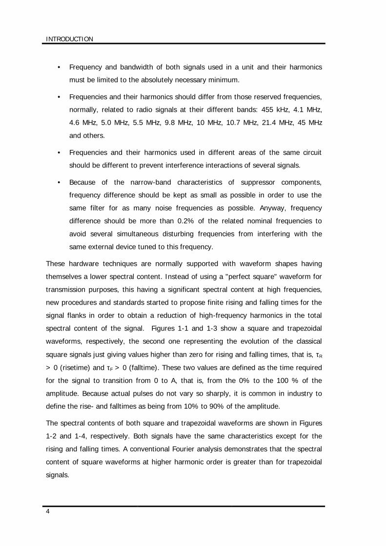
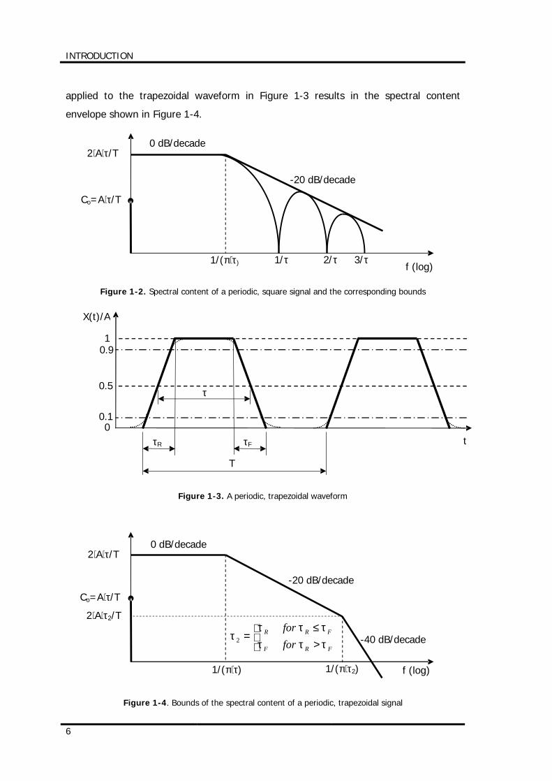
These hardware techniques are normally supported with waveform shapes having
themselves a lower spectral content. Instead of using a "perfect square" waveform for
transmission purposes, this having a significant spectral content at high frequencies,
new procedures and standards started to propose finite rising and falling times for the
signal flanks in order to obtain a reduction of high-frequency harmonics in the total
spectral content of the signal. Figures 1-1 and 1-3 show a square and trapezoidal
waveforms, respectively, the second one representing the evolution of the classical
square signals just giving values higher than zero for rising and falling times, that is, τR
> 0 (risetime) and τF > 0 (falltime). These two values are defined as the time required
for the signal to transition from 0 to A, that is, from the 0% to the 100 % of the
amplitude. Because actual pulses do not vary so sharply, it is common in industry to
define the rise- and falltimes as being from 10% to 90% of the amplitude.
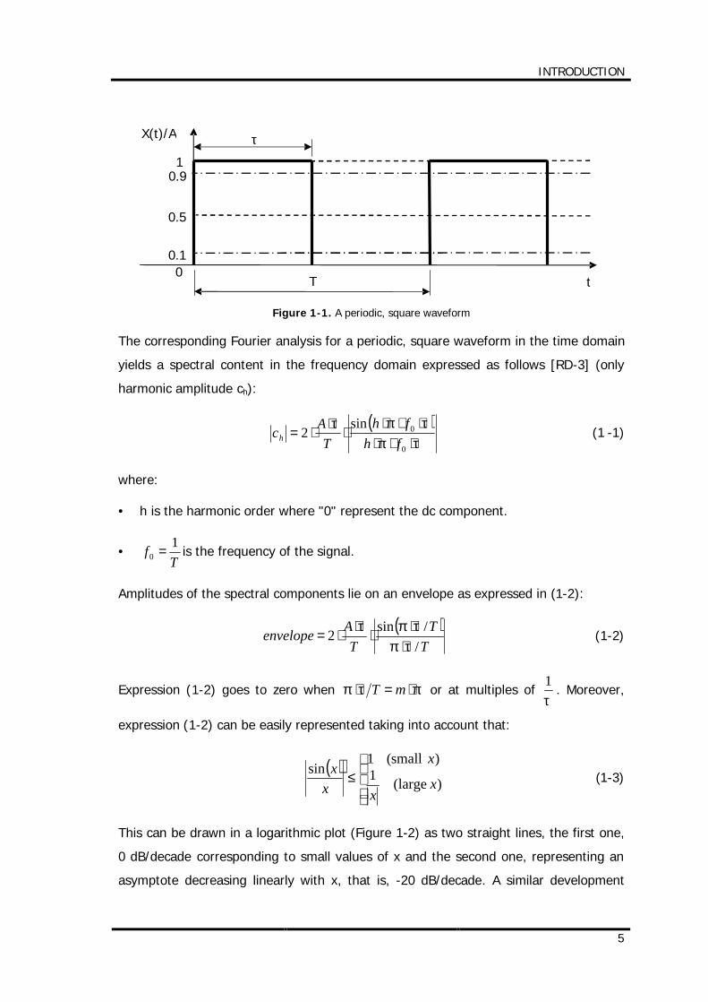
The spectral contents of both square and trapezoidal waveforms are shown in Figures
1-2 and 1-4, respectively. Both signals have the same characteristics except for the
rising and falling times. A conventional Fourier analysis demonstrates that the spectral
content of square waveforms at higher harmonic order is greater than for trapezoidal
signals.
INTRODUCTION
5
Figure 1-1. A periodic, square waveform
The corresponding Fourier analysis for a periodic, square waveform in the time domain
yields a spectral content in the frequency domain expressed as follows [RD-3] (only
harmonic amplitude ch):
( )τπ
τπτ⋅⋅⋅
⋅⋅⋅⋅
⋅⋅=
0
0sin2
fhfh
TAch (1 -1)
where:
• h is the harmonic order where "0" represent the dc component.
• T
f 10 = is the frequency of the signal.
Amplitudes of the spectral components lie on an envelope as expressed in (1-2):
( )T
TT
Aenvelope/
/sin2τπ
τπτ⋅
⋅⋅
⋅⋅= (1-2)
Expression (1-2) goes to zero when πτπ ⋅=⋅ mT or at multiples of τ1
. Moreover,
expression (1-2) can be easily represented taking into account that:
( )
≤ )large(1)small(1
sinx
x
x
xx
(1-3)
This can be drawn in a logarithmic plot (Figure 1-2) as two straight lines, the first one,
0 dB/decade corresponding to small values of x and the second one, representing an
asymptote decreasing linearly with x, that is, -20 dB/decade. A similar development
X(t)/A
0.9 1
0.5
0.1 0
τ
T t
INTRODUCTION
6
applied to the trapezoidal waveform in Figure 1-3 results in the spectral content
envelope shown in Figure 1-4.
Figure 1-2. Spectral content of a periodic, square signal and the corresponding bounds
Figure 1-3. A periodic, trapezoidal waveform
Figure 1-4. Bounds of the spectral content of a periodic, trapezoidal signal
1/(π⋅τ) 1/(π⋅τ2)
Co=A⋅τ/T
2⋅A⋅τ/T 0 dB/decade
-20 dB/decade
>≤
=FRF
FRR
forfor
ττττττ
τ 2 -40 dB/decade
2⋅A⋅τ2/T
f (log)
X(t)/A
0.9 1
0.5
0.1 0
τ
T
τR τF t
1/(π⋅τ) 1/τ 2/τ 3/τ
Co=A⋅τ/T
2⋅A⋅τ/T 0 dB/decade
-20 dB/decade
f (log)
INTRODUCTION
7
From these spectral bounds it now becomes clear that the high-frequency content of a
trapezoidal pulse train is primarily due to the rise/falltime of the pulse. Pulses having
small rise/falltimes will have larger high-frequency spectral content than those having
larger rise/falltimes. Thus, in order to reduce the high-frequency spectrum and,
consequently, the emissions of a product, the rise/falltimes of the clock, data pulses or
switching waveform should be increased as much as possible [RD-3].
This kind of signals makes part of a different concept of EMI suppression that consists
of limiting the spectral content in the signal itself. When possible, just waveforms with
a lower spectral content should be used, this way making easier, simpler and cheaper
the use of filters and other suppression means, as explained above.
In this line, EMI-reduction techniques such a Spread Spectrum Clock Generation
(SSCG) are contributing to eliminate or limit the problem at the root, that is, at the
signal itself.
1.3 State of Art
It was only in the past decade when this new technique appeared. Instead of
maintaining a constant frequency, SSCG systems modulate the clock frequency
following certain modulation profiles, thereby spreading the harmonic energy into an
amount of side-band harmonics having the same energy but smaller amplitude ([RB-1]
and [RB-2]), which normally corresponds to spreading conducted and radiated energy
over a wider frequency range.
At any frequency, the detected emissions are lower. To its proponents, SSCG held the
promise of EMI suppression by way of a clock replacement.
The history of SSCG is quite interesting. It is normally accepted that the parents of
these modulation techniques are George Antheil and the actress Hedy Lamarr. With
the help of an electrical engineering professor from the California Institute of
Technology they worked in order to become the idea in a patent, which was finally
granted on August 11th, 1942. The patent disclosed a method of frequency hopping
used to immunize radio-controlled torpedoes against jamming. In the last two decades,
the technique has become a mainstay of the communications revolutions because of its
advantages in range, immunity and security.
INTRODUCTION
8
The first published work (or, at least, it is normally said to be the first one) on the use
of Spread Spectrum Clock Generation applied to reduce EMI emissions in power
converters was a paper presented at the Virginia Power Electronics Center, Tenth
Annual Power Electronics Seminar in 1992 [RA-1]. The intention of the author was to
present how a modulation of the initially constant switching frequency controlling a
switching power supply contributed to a significant reduction of EMI emissions. In this
paper, author Lin presents a forward converter circuit and the related PWM controller
based on the Unitrode circuit UC3823. With an ingenious modification of the frequency
control of this UC3823 in order to inject not a constant but a variable frequency, it
generates a variable-frequency PWM, not affecting the duty cycle of this PWM. The
experimental verification was tested at a power supply's nominal switching frequency
of 90 kHz by following a sinusoidal modulation profile generating a frequency peak
deviation lower than 10 kHz and an adjustable modulating frequency. Anyway, some
results are also shown at frequency peak deviation of 15 kHz and modulating
frequency of 400 Hz showing a substantial reduction in emissions.
At the 1994 IEEE International Symposium on Electromagnetic Compatibility, authors
Keith B. Hardin, John T. Fessler and Donald R. Bush presented the results of their work
[RA-2]. As a difference with the previous paper [RA-1], the application field was
related to the higher frequencies world of CPU clocks in digital devices, thus giving the
fundamental jump into the area where it shows currently the biggest development.
The wide modulation frequency proposed by Lin was impractical for use as a clock
generator. The authors proposed to vary the frequency of the clock only slightly,
deviating a 20 MHz clock by a frequency peak deviation of 125 kHz (that is, ± 125 kHz
from the nominal frequency of 20 MHz), thus resulting in a variation of only 0.625%
instead of the 16.67% used by Lin. It must be kept in mind that SSCG applied to
power converters and CPU clocks have different exigencies. Anyway, this technique
resulted in a measured attenuation of the third harmonic, 60 MHz, of only 2 dB.
However, as the harmonic number increased so did the attenuation. At the 20th
harmonic, 400 MHz, the measured attenuation was 10 dB.
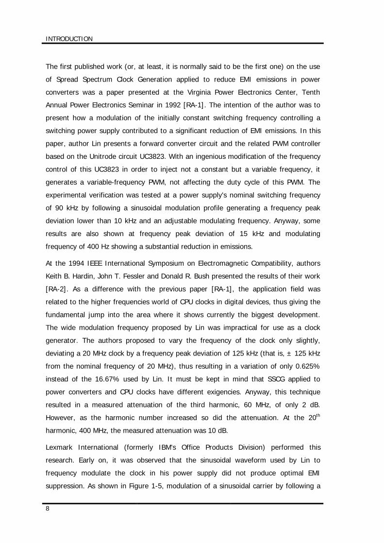
Lexmark International (formerly IBM's Office Products Division) performed this
research. Early on, it was observed that the sinusoidal waveform used by Lin to
frequency modulate the clock in his power supply did not produce optimal EMI
suppression. As shown in Figure 1-5, modulation of a sinusoidal carrier by following a
INTRODUCTION
9
sinusoidal modulating profile (Figure 1-5(a)) generates a spectrum which tends to
concentrate side-band harmonics around the two frequencies defining the bandwidth
generated during the frequency modulation process, that is, a spectrum peaked at its
extremities (Figure 1-5(b)). The reason for this effect has to do with the rate of
change, or derivative, of the sine wave. Its rate of change slows as the sine wave
reaches its peak values. That happens at the ends of the spectra in Figure 1-5(b) and
it is there that the oscillator "hangs out" a little longer than it does elsewhere. Better
results were achieved when a triangular wave was used to modulate the clock [Figures
1-5(c) and 1-5(d)]. But the engineers at Lexmark found that an optimal waveform was
that shown in Figure 1-5(e) which produced a nearly flat spectra across the deviated
range, results presented in [RA-2]. The waveform of Figure 1-5(e) has become known
as the "Lexmark Shape". Lexmark filed for, and received a patent on optimal
waveforms for use in producing a spread spectrum clock generator like that used in the
SC501AXB integrated circuit [RA-2].
(a)
(b)
(c)
(d)
(e)
(f)
Figure 1-5. Different modulation profiles (left) produce different frequency spreading effects (right)
Anyway, some points in [RA-2] are to be reconsidered in order to clarify some dark
aspects in this paper mainly related to the shape of the generated spectrum after
modulation depending on the modulation profile. A quantification of the spectrum
resulting from the modulation is also given further in the thesis.
f
dB
f
dB
f
dB
t
V
t
V
t
V
INTRODUCTION
10
It is known this paper [RA-2] was greeted with a mixture of accolades and unusually
harsh criticism but no one questioned the effect was real. Emissions detected by an
EMI receiver used in accordance with CISPR Publications 16 and 22 ([RE-1], [RE-2]
and [RE-3]) would be significantly less at the higher harmonics when SSCG was used
in place of a traditional clock. However, some engineers claimed that the technique did
not really reduce emissions, but simply "fooled" the quasi-peak detector in the EMI
receiver. That criticism, however, was unfair. A close (narrow band) look at the spectra
produced by a SSCG will reveal individual harmonics at the modulating clock frequency,
usually chosen to be between 20 and 100 kHz. Each one of the harmonics is stationary
and, therefore, will measure the same whether measured on a peak, average or a
quasi peak detector. The reason that emissions fall is that only a few of these
modulations products fall within the bandpass filter of the receiver (120 kHz) at the
higher harmonics.
Others argued that spreading the energy does not reduce it, and that receivers which
were sensitive to the total energy emitted by a digital device would not see any
improvement in their immunity due to the use of spread spectrum clock generators.
Also, receivers using bandwidths wider than 120 kHz, such as TV receivers, could be
adversely affected. The FCC rules intended to protect a wide variety of devices but
fixing a 120 kHz measuring bandwidth might be an inappropriate way to measure the
interference potential of devices employing this new technology.
The current FCC rules, and the voluntary standards upon which they are based, specify
receiver bandwidths and detectors that were developed decades ago. Anyway, the
FCC, which has already reviewed this issue once, does not see an interference threat
from SSCGs as currently implemented.
In addition, Hardin, Fessler and Bush reported on a detailed Philips Consumer
Electronics study on the effects of the use of spread spectrum clock generation in place
of fixed frequency clock on television reception ([RA-3] and [RA-11]). They concluded
that most televisions are, more or less, indifferent to the interference caused by either
a narrow band or a spread spectrum generated clock, both set to the FCC Class B
limits and centered on the same frequency. To avoid interference, the authors did
point out that the modulation frequency used should be greater than 20 kHz in order
to be beyond the audible range of the human ear. Use of a modulating frequency
above 20 kHz helps to ensure that any signals working their way through to the audio
INTRODUCTION
11
system are at frequencies high enough to be filtered out by the receiver, speaker or to
be undetectable by the human ear.
No timing considerations have been made until now. Certain applications simply cannot
tolerate a wandering clock. Video displays, for example, may shiver noticeably unless
the horizontal sweep is synchronized with the SSCG. Many forms of communications
require a synchronous clock in line with tight specifications. According to [RD-4], the
technique should not be used for timing on Ethernet, Fiber Channel, FDDI, ATM,
SONET or ADSL applications. Unless the clock is highly stable, these applications can
suffer from poor locking, failure to lock or data errors.
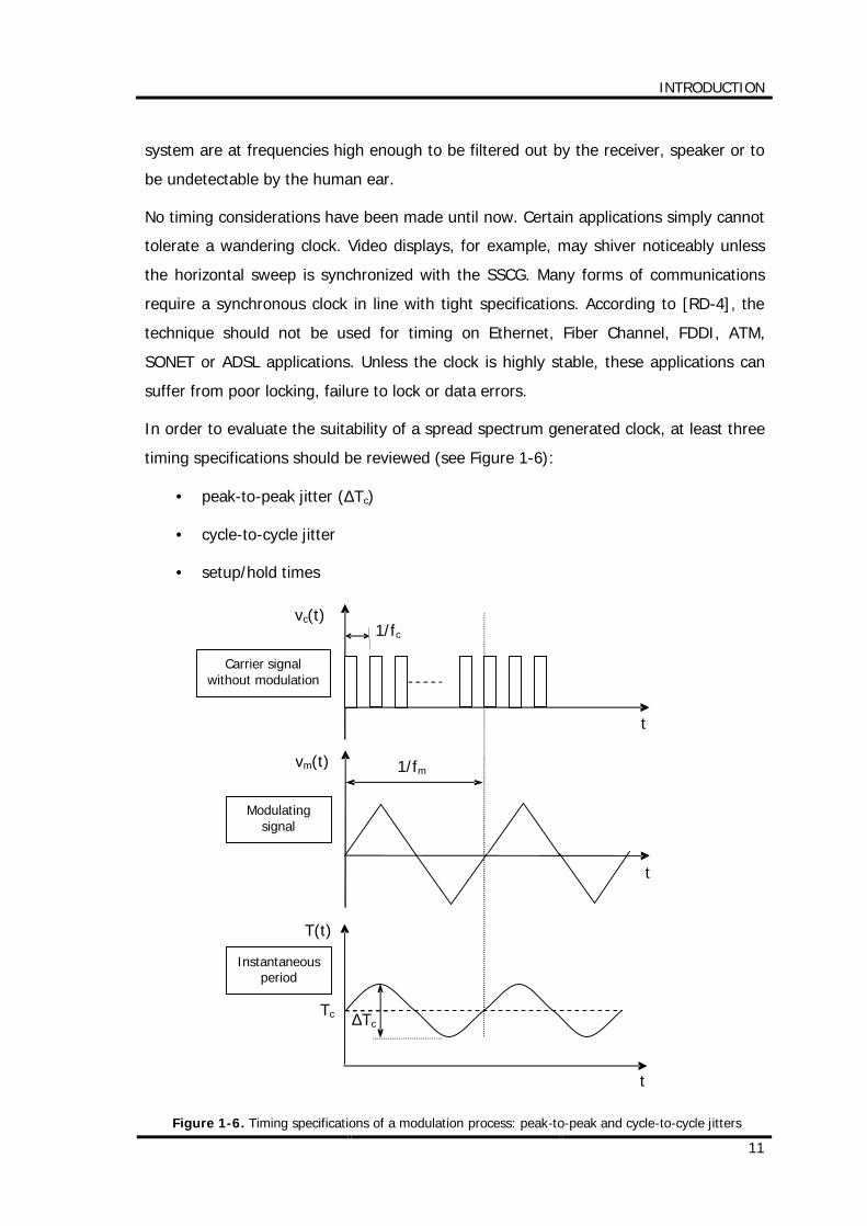
In order to evaluate the suitability of a spread spectrum generated clock, at least three
timing specifications should be reviewed (see Figure 1-6):
• peak-to-peak jitter (∆Tc)
• cycle-to-cycle jitter
• setup/hold times
Figure 1-6. Timing specifications of a modulation process: peak-to-peak and cycle-to-cycle jitters
t
T(t)
∆Tc Tc
t
vm(t) 1/fm
Instantaneous period
Modulating signal
t
vc(t) 1/fc
Carrier signal without modulation
INTRODUCTION
12
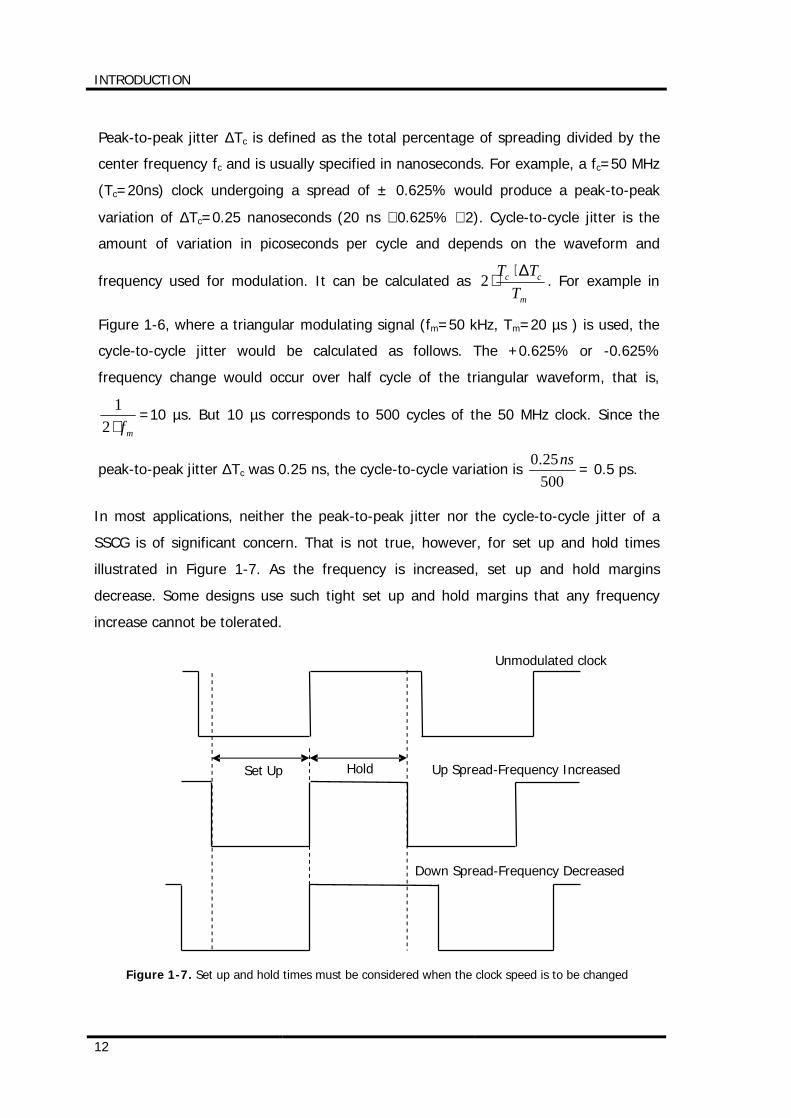
Peak-to-peak jitter ∆Tc is defined as the total percentage of spreading divided by the
center frequency fc and is usually specified in nanoseconds. For example, a fc=50 MHz
(Tc=20ns) clock undergoing a spread of ± 0.625% would produce a peak-to-peak
variation of ∆Tc=0.25 nanoseconds (20 ns ⋅ 0.625% ⋅ 2). Cycle-to-cycle jitter is the
amount of variation in picoseconds per cycle and depends on the waveform and
frequency used for modulation. It can be calculated as m
cc
TTT ∆⋅
⋅2 . For example in
Figure 1-6, where a triangular modulating signal (fm=50 kHz, Tm=20 µs ) is used, the
cycle-to-cycle jitter would be calculated as follows. The +0.625% or -0.625%
frequency change would occur over half cycle of the triangular waveform, that is,
mf⋅21
=10 µs. But 10 µs corresponds to 500 cycles of the 50 MHz clock. Since the
peak-to-peak jitter ∆Tc was 0.25 ns, the cycle-to-cycle variation is 50025.0 ns
= 0.5 ps.
In most applications, neither the peak-to-peak jitter nor the cycle-to-cycle jitter of a
SSCG is of significant concern. That is not true, however, for set up and hold times
illustrated in Figure 1-7. As the frequency is increased, set up and hold margins
decrease. Some designs use such tight set up and hold margins that any frequency
increase cannot be tolerated.
Figure 1-7. Set up and hold times must be considered when the clock speed is to be changed
Set Up Hold
Unmodulated clock
Up Spread-Frequency Increased
Down Spread-Frequency Decreased
INTRODUCTION
13
For this reason, spread spectrum clock generation is sometimes implemented using a
"down spreading" only technique. Instead of shifting the clock frequency above or
below around the narrow band carrier, the frequency is only shifted downwards, which
should only increase the setup and hold margins. One of the most challenging
applications for spread spectrum clock generation is its use in Pentium based
machines. Techniques such as down spreading can resolve most timing concerns.
However, use of a spread spectrum clock generator in these high performance designs
is not easy. The reason for this is the internal multiplication that is used to increase
clock speed. As mentioned, this internal multiplication is done by way of a phase
locked loop (PLL). A PLL uses a feedback system to compare a frequency-divided
version of the output signal to the input signal, thereby locking the two in frequency.
Like most feedback systems, however, an instantaneous change at the input does not
result in an instantaneous proportional change at the output. Rather, the output can
approach its final value asymptotically (as in a single pole, "overdamped" feedback
system) or bounce around its final value (as in the case of a multiple order,
"underdamped" system). Most phase locked loops used for frequency multiplication in
CPUs are third order, making predictions as to how the output frequency will change
with changes to the input frequency non trivial [RA-5].
1.4 Generic structure of the thesis
This thesis is developed logically in several parts, corresponding to different chapters.
A summary of these chapters is presented onwards:
• In chapter 2, a wide theoretical development of the modulation and related
concepts are presented. It is explained generically all aspects related to the
modulation and particularly, to the frequency modulation. Main parameters of
frequency modulation are presented and explained in detail and how practical
considerations may affect to the theoretical behaviour of these parameters.
Because the theoretical part of this thesis is completely based on the fundaments
of the Fourier Transform, a sufficient explanation was thought to include for a right
understanding of this thesis (Annex 3). Finally, all this knowledge is summarized in
a computational algorithm (MATLAB environment), capable of generating any
frequency modulation of a sinusoidal carrier and the corresponding spectral
components resulting from the modulation process.
INTRODUCTION
14
• Chapter 3 takes profit of the results obtained in Chapter 2 where it is possible to
obtain the theoretical behaviour of the different modulation profiles of interest:
sinusoidal, triangular, exponential and mixed waveforms. This way, chapter 3 is
intended to completely understand and analyze the theoretical behaviour of these
modulation profiles and be quantified according to several significant measure
parameters. Afterwards, a comparison of these modulation profiles is carried out by
means of the measure parameters defined previously. A proposal of control for a
real power converter and theoretical considerations to apply a certain SSCG
method to switching power converters are also included in this chapter.
• After all aspects of frequency modulation by means of SSCG methods have been
theoretically developed, it is mandatory the verification of the theoretical
conclusions through an experimental test plant. Chapter 4 starts with the
description, theoretical calculation and physical implementation of this test plant.
Most practical considerations are here dealt with, like the influence of the Spectrum
Analyzer's Resolution Bandwidth (RBW) on the measured EMI, a proposal of a
practical method to select a valuable SSCG technique applied to Switching Power
Converters, comparative measurements of conducted EMI within the range of
conducted emissions (0 Hz ÷ 30 MHz) and a proposal about SSCG as a method to
avoid interfering a certain signal.
• Chapter 5 summarizes the whole conclusions gathered through the previous
chapters and, finally, chapter 6 lists references related to the thesis, separated into
different thematic groups.
• Several annexes have been included at the end of this document. Some of them
are direct references to the thesis and the rest are included because they were
considered to be of interest, like the one entitled "CONSIDERATIONS ABOUT EMC
UNITS EXPRESSED IN DECIBELS".
1.5 Experimental considerations and operative guideline
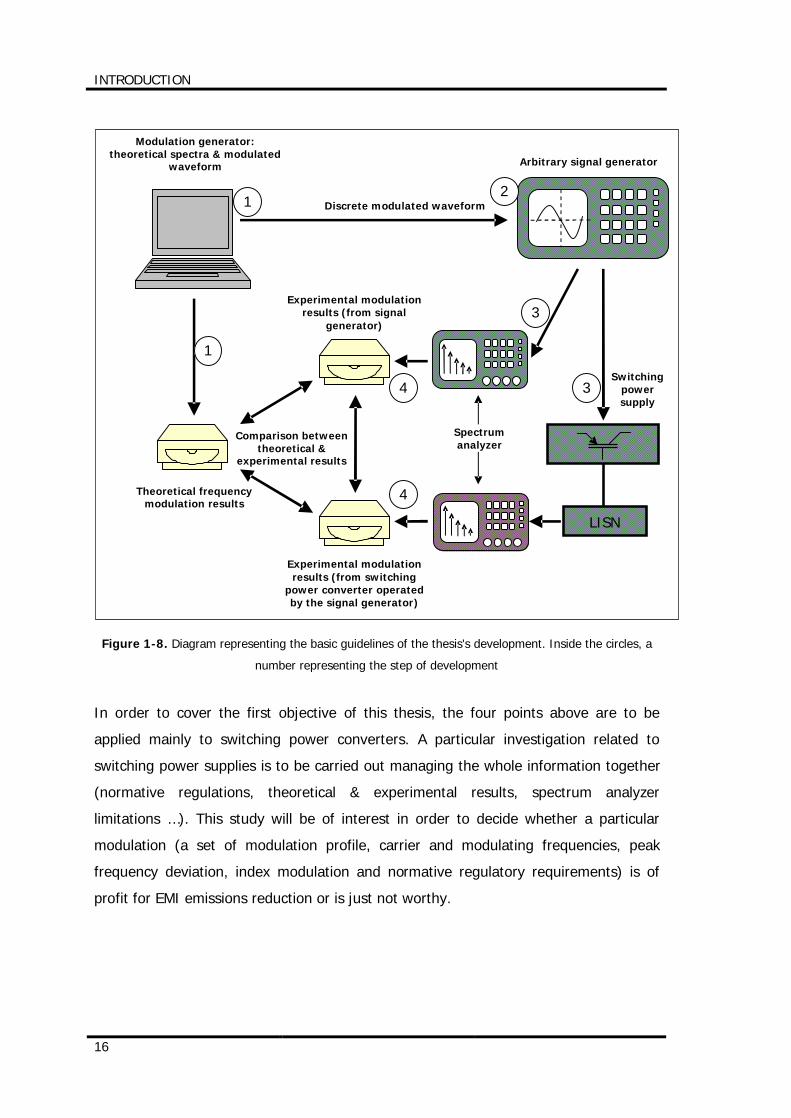
Diagram in Figure 1-8 summarizes the operative guideline of this thesis:
1. Development of a mathematical model and working environment. It will gather the
whole concepts, parameters and expressions related to frequency modulation and
its particular focus on SSCG. Further, this model is to be concretized in a
INTRODUCTION
15
computational algorithm, this one generating both modulated waveforms to be
introduced into an arbitrary function generator and the theoretical results of the
different frequency modulations under test.
Profile modulations to be applied include sinusoidal, triangular and exponential
modulating waveforms as analytical expressions but also sampled modulating
waveforms and other specific modulating waveforms will be an available option.
2. The waveform resulting from the selected mathematical modulation will be
introduced into an arbitrary signal generator. Special care must be taken when
selecting the characteristics and performance of this equipment.
3. The modulated signal coming out from the signal generator is then introduced
either into a specific switching power converter (in order to control it) or directly
into the spectrum analyzer. In the first case, the EMI emissions are measured by
using a compliant LISN (Line Impedance Stabilization Network), whose output is
directed to the input of the spectrum analyzer. A detailed explanation of how a
spectrum analyzer works is mandatory for a perfect understanding of the further
experimental results (Annex 1). A broad explanation of measurement normative
requirements will be also exposed (Annex 2) in order to show that true EMI
emissions reduction can be faded by regulatory exigencies.
4. The two different types of experimental results (those generated by the
measurement of modulation directly from the output of the signal generator and
those coming from the LISN) can be useful to decide whether their differences are
due to the modulation processes themselves or just because of the experimental
plant being used. In a first approach, experimental results from measurements
taken directly from the output of the signal generator should be nearly the same as
those obtained in theoretical calculations; however, those results from
measurements through a switching power converter and the corresponding LISN
should be affected by the plant's characteristics as component behaviour (recovery
time of diodes, switching of the power transistor ON ↔ OFF, coupled capacitances
and so on). A description of the experimental plant is to be presented in detail in
chapter 4.
INTRODUCTION
16
Figure 1-8. Diagram representing the basic guidelines of the thesis's development. Inside the circles, a
number representing the step of development
In order to cover the first objective of this thesis, the four points above are to be
applied mainly to switching power converters. A particular investigation related to
switching power supplies is to be carried out managing the whole information together
(normative regulations, theoretical & experimental results, spectrum analyzer
limitations …). This study will be of interest in order to decide whether a particular
modulation (a set of modulation profile, carrier and modulating frequencies, peak
frequency deviation, index modulation and normative regulatory requirements) is of
profit for EMI emissions reduction or is just not worthy.
Arbitrary signal generator
Theoretical frequency modulation results
Experimental modulation results (from signal
generator)
Experimental modulation results (from switching
power converter operated by the signal generator)
Modulation generator: theoretical spectra & modulated
waveform
LISN
Comparison between theoretical &
experimental results
Spectrum analyzer
Switching power supply
Discrete modulated waveform 1 2
1
3
3 4
4
C H A P T E R
2
THEORETICAL BASIS

THEORETICAL BASIS
19
2. THEORETICAL BASIS
This chapter is intended to introduce all aspects related to the modulation and
particularly, to the frequency modulation, because this is the kind of modulation used
to generate SSCG (Spread Spectrum Clock Generation) methods in this thesis. A wide
theoretical development of the modulation and related concepts are presented as well
as the main parameters of frequency modulation and how practical considerations may
affect to the theoretical behaviour of these parameters. Although the theoretical
development here presented considers only the modulation of a sinusoidal waveform,
it is also demonstrated the validity and extension of these results to a generic signal.
Because the theoretical part of this thesis is completely based on the fundaments of
the Fourier Transform, a sufficient explanation was included for a right understanding
of the thesis (Annex 3). Finally, all this knowledge is summarized in a computational
algorithm (MATLAB environment), capable of generating any frequency modulation of
a sinusoidal carrier and the corresponding spectral components resulting from the
modulation process. A verification procedure for this algorithm is also presented in
order to validate one of the most important parts of the thesis.
2.1 Modulation
Modulation is the process by which some characteristics of a carrier waveform are
modified by another signal in order to obtain some benefits [RD-1]. This process of
modulation is widely used in telecommunications (both video and audio signals) where
the information of a signal is transferred to the carrier before transmission.
The characteristics of the carrier being modulated are normally amplitude and/or
frequency. In its simplest way, a modulator can vary such characteristics of the carrier
proportionally to the modulating waveform: this is called analogical modulation. More
complicated modulators make first a conversion to digital and codify the modulating
signal before modulation; this is known as a digital modulation.
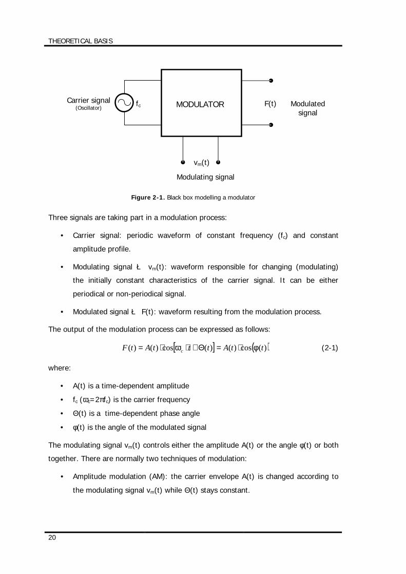
In order to understand the process of modulation, it is a good procedure to present a
modulator as a black box with two inputs and one output (Figure 2-1):
THEORETICAL BASIS
20
Figure 2-1. Black box modelling a modulator
Three signals are taking part in a modulation process:
• Carrier signal: periodic waveform of constant frequency (fc) and constant
amplitude profile.
• Modulating signal è vm(t): waveform responsible for changing (modulating)
the initially constant characteristics of the carrier signal. It can be either
periodical or non-periodical signal.
• Modulated signal è F(t): waveform resulting from the modulation process.
The output of the modulation process can be expressed as follows:
[ ] ( ))(cos)()(cos)()( ttAtttAtF c φω ⋅=Θ+⋅⋅= (2-1)
where:
• A(t) is a time-dependent amplitude
• fc (ωc=2πfc) is the carrier frequency
• Θ(t) is a time-dependent phase angle
• φ(t) is the angle of the modulated signal
The modulating signal vm(t) controls either the amplitude A(t) or the angle φ(t) or both
together. There are normally two techniques of modulation:
• Amplitude modulation (AM): the carrier envelope A(t) is changed according to
the modulating signal vm(t) while Θ(t) stays constant.
MODULATOR Modulated signal
Carrier signal (Oscillator)
F(t)
vm(t)
Modulating signal
fc
THEORETICAL BASIS
21
• Angle modulation: A(t) is a constant value A but the angle φ(t) is controlled by
the modulating signal vm(t). This angle modulation has two variants depending
on the close relationship between the angle φ(t) and the modulating signal:
o Phase modulation (PM)
o Frequency modulation (FM)
Because frequency modulation is the base of this thesis, a more detailed explanation of
it is required.
2.1.1 Frequency Modulation (FM)
Systems based on angle modulation show a very good insensitiveness to fluctuations
due to noise, particularly, impulse noise when used in communications. Onwards, some
concepts related to FM are presented in order to frame further developments. A more
detailed explanation can be found in reference [RD-1] and others.
2.1.1.1 Generic Formulation of Frequency Modulation
In frequency modulation, the deviation (δω) of instantaneous frequency ω(t) respect to
the constant carrier frequency ωc is directly proportional to the instantaneous
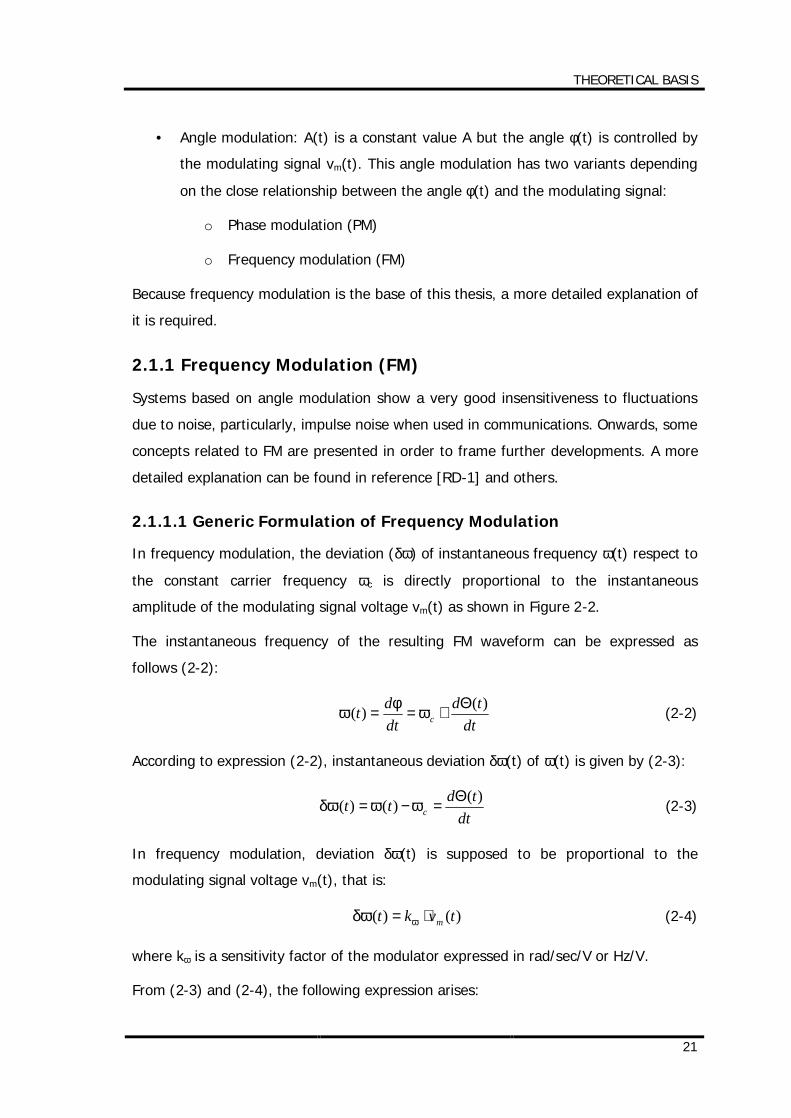
amplitude of the modulating signal voltage vm(t) as shown in Figure 2-2.
The instantaneous frequency of the resulting FM waveform can be expressed as
follows (2-2):
dttd
dtdt c
)()( Θ+== ω
φω (2-2)
According to expression (2-2), instantaneous deviation δω(t) of ω(t) is given by (2-3):
dttdtt c)()()( Θ
=−= ωωδω (2-3)
In frequency modulation, deviation δω(t) is supposed to be proportional to the
modulating signal voltage vm(t), that is:
)()( tvkt m⋅= ωδω (2-4)
where kω is a sensitivity factor of the modulator expressed in rad/sec/V or Hz/V.
From (2-3) and (2-4), the following expression arises:
THEORETICAL BASIS
22
)0()()(0
Θ+⋅⋅=Θ ∫t
m dttvkt ω (2-5)
where Θ(0) is the initial value of phase and it is commonly taken as zero.
Figure 2-2. Effect of sinusoidal frequency modulation. (a) modulating wave; (b) instantaneous frequency
of the FM waveform; (c) instantaneous angle of the FM waveform.
From (2-1) and (2-5), the generic expression of a frequency modulated sinusoidal
waveform F(t) takes this aspect:
⋅⋅+⋅⋅= ∫
t
mc dttvktAtF0
)(cos)( ωω (2-6)
A very important ratio in frequency modulation is known as modulation index mf and is
expressed this way:
t
vm(t)
t
ω(t)
∆ωc ωc
(a)
(b)
φ(t)
t
(c) ωc t
1/fm
THEORETICAL BASIS
23
m
c
m
cf f
fm ∆=
∆=
ωω
(2-7)
where (according to Figure 2-2(b)):
• ∆fc is the peak deviation of the carrier frequency.
• fm is the frequency of the modulating signal vm(t), assuming it is a periodic
waveform.
2.1.1.2 Other important parameters
Some other parameters and concepts are to be used along the thesis. The following
ones are the most important:
2.1.1.2.1 Modulation ratio δ
The modulation ratio denotes the peak excursion of the switching or carrier frequency
referred to itself, that is:
c
c
ff∆
=δ (2-8)
When the modulation ratio is expressed in %, it is more usually known as percentage
of modulation δ%:
100% ⋅∆
=c
c
ff
δ (2-9)
This percentage of modulation normally ranges between 1% and 2.5% for the
commercial applications [RC-5] at higher frequencies (in order to conserve the
minimum-period requirements for control system timing). In the case of switching
power converters, where timing requirements are much less important, this percentage
can be larger, much more than 2.5%. This will be studied in the thesis later on.
2.1.1.2.2 Modulation profiles
The most important parameter defining the shape of the resulting modulated wave
spectrum is strongly related to the modulation profile, that is, the shape of the
waveform used to modulate but these profiles also influence the displacement of the
central frequency up- or down-wards respect to the original signal, as shown in Figure
2-3.
THEORETICAL BASIS
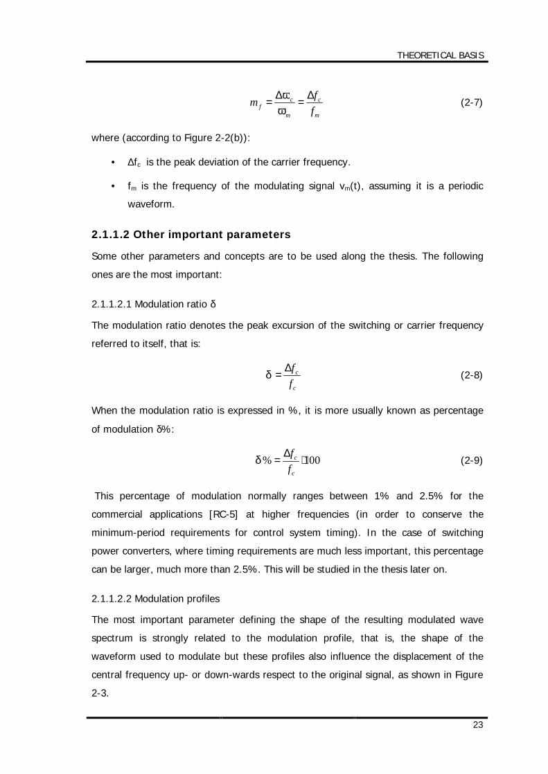
24
Instead of shifting the carrier frequency above and below symmetrically, the frequency
is only shifted up or downwards respect to the carrier.
Figure 2-3. a) Down-spreading, b) symmetrical and c) up-spreading SSCG techniques
Where setup and hold time margins are critical, down spreading technique is preferred.
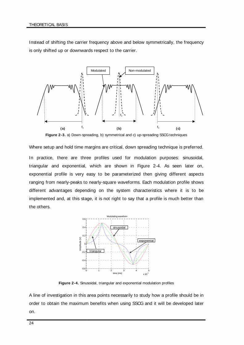
In practice, there are three profiles used for modulation purposes: sinusoidal,
triangular and exponential, which are shown in Figure 2-4. As seen later on,
exponential profile is very easy to be parameterized then giving different aspects
ranging from nearly-peaks to nearly-square waveforms. Each modulation profile shows
different advantages depending on the system characteristics where it is to be
implemented and, at this stage, it is not right to say that a profile is much better than
the others.
0 1 2 3 4 5x 10 -3
-0.6
-0.4
-0.2
0
0.2
0.4
0.6Modulating waveform
time (ms)
Ampl
itude
(V)
Figure 2-4. Sinusoidal, triangular and exponential modulation profiles
A line of investigation in this area points necessarily to study how a profile should be in
order to obtain the maximum benefits when using SSCG and it will be developed later
on.
fc fc
fc
Non-modulated Modulated
(a) (b) (c)
exponential
sinusoidal
triangular
THEORETICAL BASIS
25
2.1.2 Bandwidth of the FM waveform
Bandwidth is defined as the difference between the limiting frequencies within which
performance of a device, in respect to some characteristic, falls within specified limits
or the difference between the limiting frequencies of a continuous frequency band.
An FM signal actually contains an infinite number of side frequencies besides the
carrier and therefore occupies infinite bandwidth. However, the side frequencies
quickly decrease in strength and can be considered negligible at some point. In
practice, a tradeoff between bandwidth and distortion must be considered.
The bandwidth of a frequency modulated waveform is approximately given by the
Carson’s rule (valid for any angle-modulated signal) and can be summarized as follows
[RD-3]:
− Total energy of the original signal keeps unaffected
− The 98% of the total energy is contained inside a bandwidth B calculated as
follows:
( )mcfm ffmfB +∆⋅=+⋅⋅= 2)1(2 (2-10)
where:
− fm represents the highest modulating frequency.
− ∆fc is the peak deviation of the carrier frequency.
− Modulation index is defined as m
cf f
fm ∆= .
2.1.3 Sinusoidal carrier vs. a generic carrier: validity of
modulation results
Until this point, all considerations and developments have taken into account the fact
of modulating a sinusoidal carrier. Most of the carriers (even those intended to be
sinusoidal) are not a pure sine wave but a set of harmonics. In switching power
converters, a PWM signal is to be found; microprocessor systems will be activated by a
square clock signal and communication standards define normally trapezoidal
waveforms in order to reduce the high-frequency spectral components [see Figures 1-3
and 1-4 in clause 1.2]. The question now is how to deal with these generic waveforms
consisting of infinity of harmonics.
THEORETICAL BASIS
26
2.1.3.1 Spectral content of a signal [RD-3] & [RD-8]
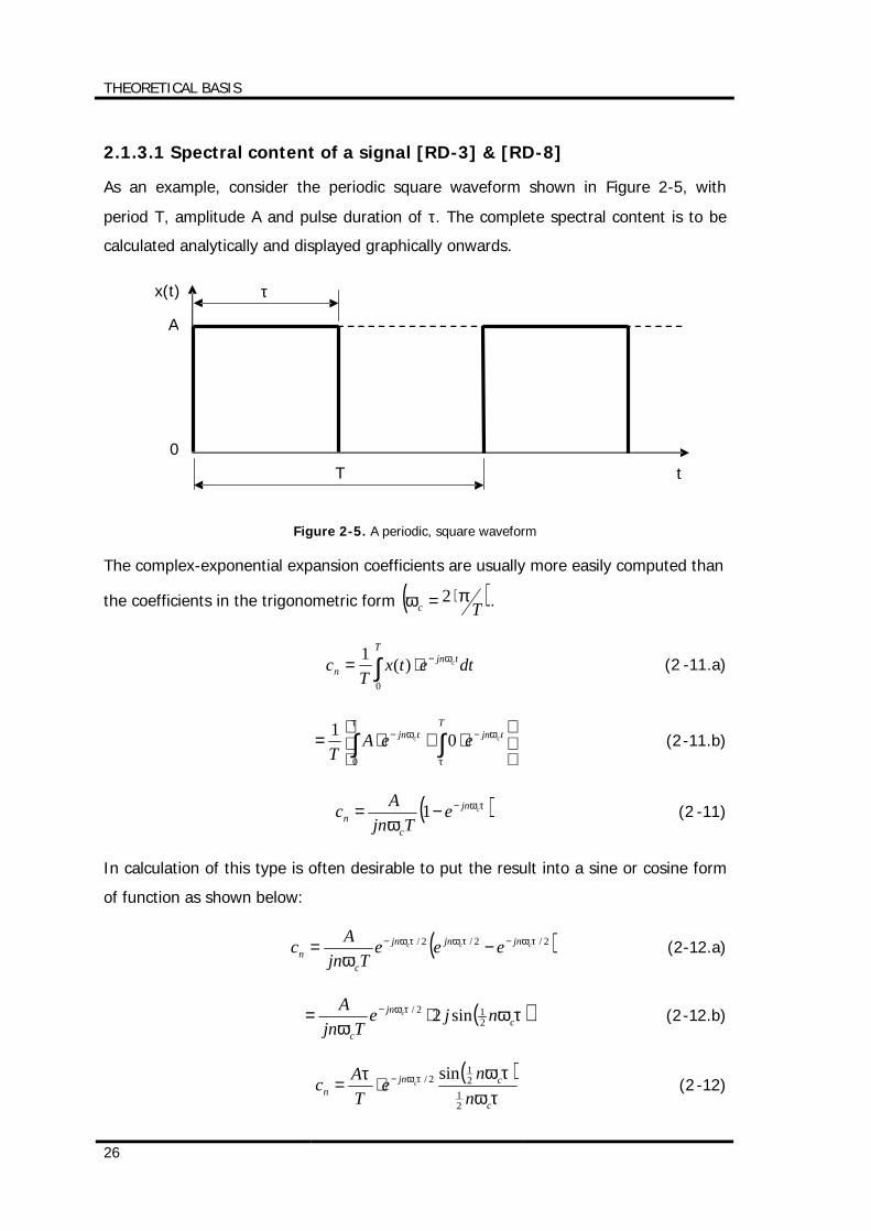
As an example, consider the periodic square waveform shown in Figure 2-5, with
period T, amplitude A and pulse duration of τ. The complete spectral content is to be
calculated analytically and displayed graphically onwards.
Figure 2-5. A periodic, square waveform
The complex-exponential expansion coefficients are usually more easily computed than
the coefficients in the trigonometric form ( )Tcπω ⋅= 2 .
∫ −⋅=T
tjnn dtetx
Tc c
0
)(1 ω (2 -11.a)
⋅+⋅= ∫∫ −−
Ttjntjn cc eeA
T τ
ωτ
ω 01
0
(2-11.b)
( )τω
ωcjn
cn e
TjnAc −−= 1 (2 -11)
In calculation of this type is often desirable to put the result into a sine or cosine form
of function as shown below:
( )2/2/2/ τωτωτω
ωccc jnjnjn
cn eee
TjnAc −− −= (2-12.a)
( )τωω
τωc
jn
c
njeTjn
Ac
212/ sin2⋅= − (2-12.b)
( )τω
τωτ τω
c
cjnn n
neTAc c
21
21
2/ sin−⋅= (2 -12)
A
0
τ
T t
x(t)
THEORETICAL BASIS
27
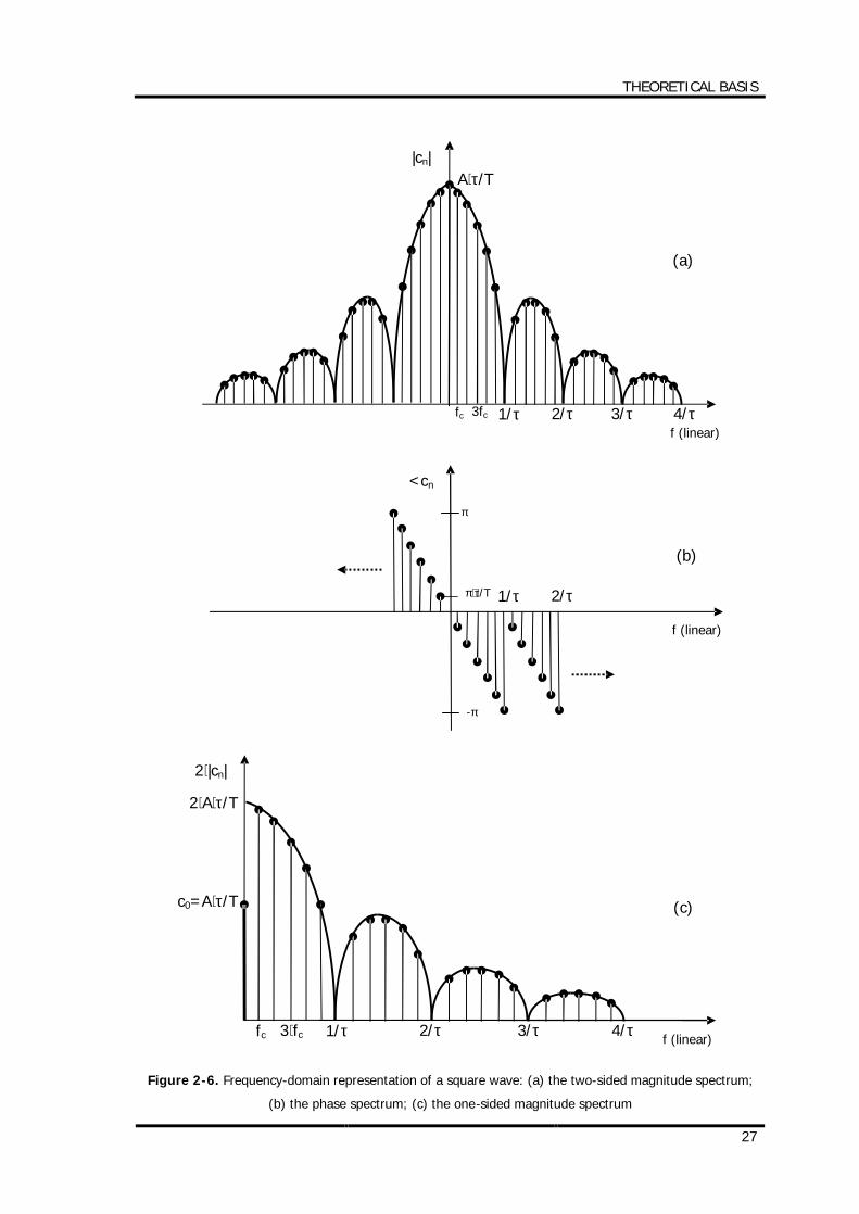
Figure 2-6. Frequency-domain representation of a square wave: (a) the two-sided magnitude spectrum;
(b) the phase spectrum; (c) the one-sided magnitude spectrum
f (linear) 1/τ 2/τ 3/τ 4/τ
A⋅τ/T |cn|
f (linear)
π⋅τ/T
<cn
(a)
(b)
fc 3fc
1/τ 2/τ
π
-π
1/τ 2/τ 3/τ
c0=A⋅τ/T
2⋅A⋅τ/T
f (linear) 4/τ
(c)
fc 3⋅fc
2⋅|cn|
THEORETICAL BASIS
28
From the result above, the following two expressions corresponding to the module and
phase of the n-harmonic can be derived:
( )
τωτωτ
c
cn n
nTAc
21
21sin
⋅= (2 -13)
τωcn nc 21±=∠ (2 -14)
or, in terms of period T ( Tcπω 2= ):
( )
TnTn
TAcn /
/sinπτ
πττ⋅= (2 -15)
Tncn
πτ±=∠ (2 -16)
The ± sign of the angle comes about because the ( )τωcn21sin term may be positive or
negative (an angle of 180º). This is added to the angle of 2/τωcjne− .
A usual convention is displaying both positive and negative frequency sinusoids for
each frequency and halving the amplitude accordingly, as in Figure 2-6(a). A more
intuitive convention is related to represent only positive frequency sinusoids, which is
achieved by doubling the amplitude of each individual component, as shown in Figure
2-6(c).
How every spectral component is affected by the modulation process is clarified in the
next clause.
2.1.3.2 Impact of modulation on every spectral component
The distance in frequency between two consecutives harmonics is given by the
frequency fc of the original signal (supposing to be periodic). The frequency fh of the
harmonic Fh is expressed this way:
ch fhf ⋅= (2 -17)
where h is the harmonic order varying from 0 to ∞.
Each harmonic component is represented as a pair amplitude-phase (Ah-θh) at a
frequency position fh and is equivalent to a pure sinusoidal waveform with the only
consideration of not being independent but making part of a "bigger" signal (see
Figure 2-6):
THEORETICAL BASIS
29
( )hchh thAtF θω +⋅⋅⋅= cos)( (2 -18)
If the same frequency modulation is applied to each harmonic component, expressions
(2-1), (2-3) and (2-4) can be generalized as follows, respectively:
[ ] ( ))(cos)()(cos)()(mod ttAtthtAtF hhhchh φω ⋅=Θ+⋅⋅⋅= (2-19)
dttdhtt h
chh)()()( Θ
=⋅−= ωωδω (2-20)
)()()( tvkhtvkt mmh
h ⋅⋅=⋅= ωωδω (2-21)
where kωh in (2-21) was defined for similarity with expression (2-4) .
From (2-19), (2-20) and (2-21), the generic expression of a frequency modulated
harmonic component is:
⋅⋅++⋅⋅⋅= ∫
t
mh
hchh dttvkthAtF0
mod )(cos)( ωθω (2-22)
and
∫ ⋅⋅+=Θt
mh
hh dttvkt0
)()( ωθ (2-23)
Some conclusions can be obtained from the expressions above:
• From (2-20) and (2-23), the particular harmonic phase θh does not affect the
results of frequency modulation because of the derivative behaviour of the
frequency deviation as expressed in (2-20) and demonstrated further in clause
2.2.3.3.
• From (2-17), the peak frequency deviation affecting each harmonic component
increases linearly with the harmonic order, that is, ch fhf ∆⋅=∆ . In other words,
the modulation index related to each harmonic component hfm will also
increase linearly with the harmonic order:
fm
c
m
hhf mh
ffh
ffm ⋅=
∆⋅=
∆= (2 -24)
• The bandwidth Bh of the frequency modulated harmonic component h increases
also linearly with the harmonic order:
THEORETICAL BASIS
30
( )mhhfmh ffmfB +∆⋅=+⋅⋅= 2)1(2 (2-25)
that is,
)1(2 −⋅∆⋅+= hfBB ch (2-26)
)1(2 −⋅⋅⋅+= hmfBB fmh (2-27)
where B is the bandwidth corresponding to modulation of a sinusoidal
waveform of frequency fc, equivalent to the 1st harmonic of the generic
waveform.
2.2 Practical considerations related to FM parameters
It is important to distinguish between a phenomenon itself and the way it is measured.
Although theoretical results show a good performance of frequency modulation
regarding to EMI emissions reduction in every case (as demonstrated in chapter 3),
measurements procedures (normally related to practical limitations of measure
equipment or normative aspects) can fade such a good behaviour even making it
negligible. In other words, a good theoretical SSCG system is not a guarantee of a
good experimental result when measuring; it should be only taken as a start point
which, after some modifications, could work properly. Onwards, some practical
considerations related to each FM parameter together with its theoretical implication
are to be exposed.
2.2.1 Carrier (Switching) & modulating frequencies
As exposed previously, the carrier (switching) signal is the constant frequency (fc)
wave to be modulated, while the modulating signal (normally a constant frequency [fm]
wave) is the waveform used to do the modulation.
Fourier series is a common way to express any waveform:
∑∞
=
+=1
0 )()(h
h tFFtF (2-28)
where F0 represents the average (dc) component of the original signal and Fh, each
one of the infinity of harmonics.
THEORETICAL BASIS
31
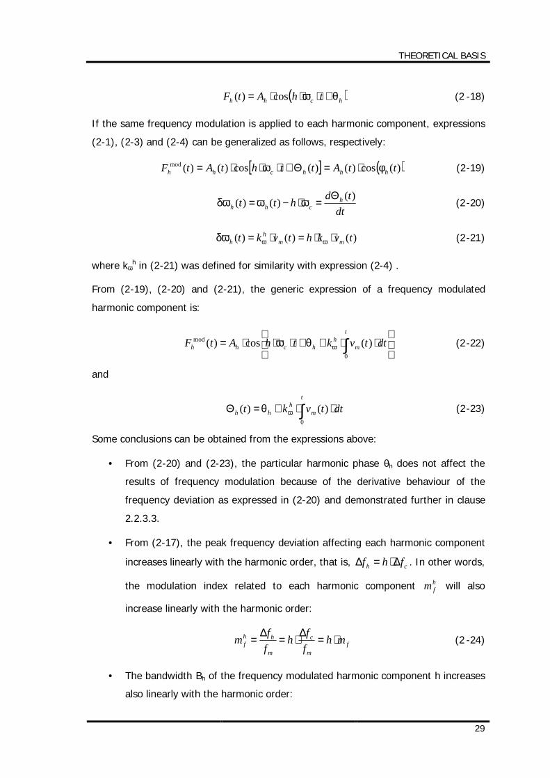
When talking about modulation of a base frequency (no matter the kind of modulation:
square, triangular, sinusoidal, exponential, random, etc), a common way to operate is
modulating each individual component Fh of the base waveform (onwards, main
harmonics) and, then, obtaining a window of sub-harmonics (onwards, side-band
harmonics) for each main harmonic (see Figure 2-7).
Figure 2-7. Only one modulating signal modulates every harmonic of the original signal.
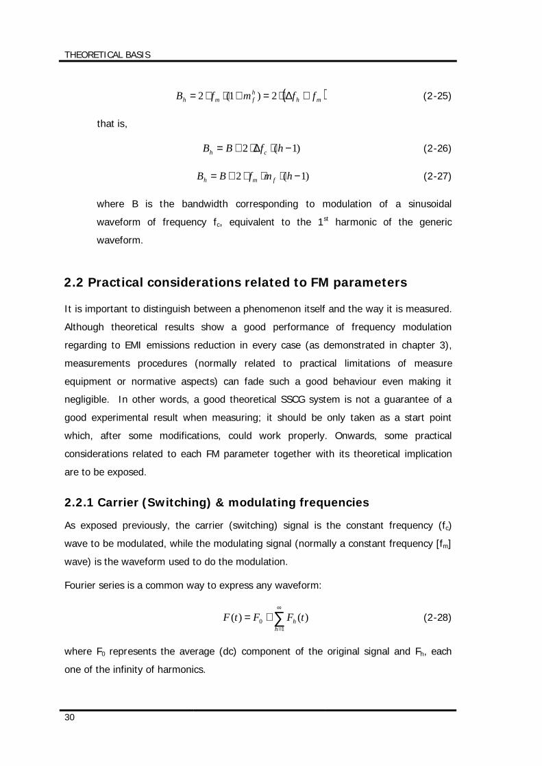
As expressed in (2-10), the bandwidth of the side-band harmonics increases linearly
with the carrier frequency fc, the modulation ratio δ and the modulating frequency fm.
For frequency modulation, the distance between two consecutive side-band harmonics
is given by the modulating frequency fm (see Figure 2-8). This frequency is usually
selected to be larger than 30 kHz in order to be above the audio band.
Figure 2-8. Distance between two consecutive side-band harmonics (FM modulation)
Common values for the modulating frequency fm range from 50 kHz to 250 kHz [RC-5]
(for system clocks). No commercial information is available for power converters
related to modulating frequency but it is advisable to use smaller modulating
frequencies depending on the application ([RB-1] & [RB-2]). In the same way, CISPR
16-1 specifies several RBWs (6 dB) for the different frequency ranges and
f
dBV
dBVref
Main harmonics of the signal
Window of sub-harmonics
fm
Bandwidth (B)

THEORETICAL BASIS
32
measurement modes. This way, a RBW of 220 Hz is intended for measurements in the
band A (9 kHz-150 kHz); 9 kHz for the band B (150 kHz-30MHz); 120 kHz for the
bands C (30 MHz-300 MHz) and D (300 MHz-1GHz) and 1 MHz for frequencies higher
than 1 GHz (valid for quasi-peak, peak and average measurement mode).
The spectrum analyzer band-pass filter (commonly known as Resolution Bandwidth-
RBW) is adjustable, for instance, to accomplish the value defined in a regulatory norm.
Two main cases are of significance (see clauses 4.2 and 4.3):
• fm < RBW: It is not possible to distinguish individual side-band harmonics, so
the measured value will be higher than expected in theoretical calculations but
it can still be worthy if RBW < B (see Figure 2-8).
• fm > RBW: Considering no overlap exists, the measured value corresponds to
the actual individual side-band harmonic amplitude.
For the second case (fm > RBW) to be reached for the different frequency ranges
expressed above, special care must be taken when selecting the modulating frequency.
As the sum of the several side-band harmonics inside this RBW is done by just adding
amplitudes (this represents the way a spectrum analyzer actually adds signals in its
bandwidth according to [RD-3] and Annex 1), it is expected to obtain (for the first
case) a value higher than the actual one. The larger RBW, the larger the measured
value for each side-band harmonic too.
2.2.2 Carrier frequency peak deviation ∆fc (Overlap)
Carrier frequency peak deviation ∆fc denotes the peak excursion of the switching
frequency fc and it is normally expressed as cc ff ⋅=∆ δ , where the factorδ is the
modulation ratio. The resulting window bandwidth B (already presented in expression
(2-10)) depends on the modulation ratio δ and it is desired that the side-band
frequencies do not fall into the audible range. It is important to remind that the
bandwidth resulting from modulation process is wider than two times the carrier
frequency peak deviation, the first one given by the Carson's rule.
According to Figure 2-9 and expression (2-25), derived in clause 2.1.3.2 and
reproduced below,
( )mhhfmh ffmfB +∆⋅=+⋅⋅= 2)1(2 (2-25)
THEORETICAL BASIS
33
and taking into account that audio problems occur normally at h=1, the following
sequence of expressions can be derived (note that fc=f1):
max,1
2 audc fBf >− (2-29)
( ) max,audmcc ffff >+∆− (2 -30)
( ) max,audmcc ffff >+⋅− δ (2 -31)
( ) maudc fff +>−⋅ max,1 δ (2-32)
where faud,max represents the higher limit of the human audible frequencies.
Expression (2-32) should be accomplished in order to avoid undesirable audio
interferences. Note that switching frequencies of power converters are usually low (fc <
1MHz) and special care must be taken to avoid harmonics into the audible band
(faud,min=20 Hz < faud < faud,max=20 kHz).
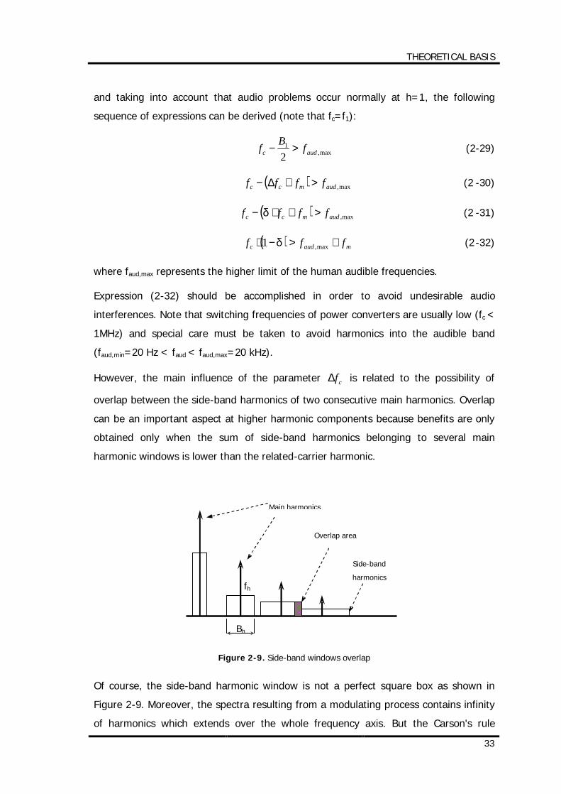
However, the main influence of the parameter cf∆ is related to the possibility of
overlap between the side-band harmonics of two consecutive main harmonics. Overlap
can be an important aspect at higher harmonic components because benefits are only
obtained only when the sum of side-band harmonics belonging to several main
harmonic windows is lower than the related-carrier harmonic.
Figure 2-9. Side-band windows overlap
Of course, the side-band harmonic window is not a perfect square box as shown in
Figure 2-9. Moreover, the spectra resulting from a modulating process contains infinity
of harmonics which extends over the whole frequency axis. But the Carson's rule
Overlap area
Main harmonics
Side-band
harmonics
Bh
fh
THEORETICAL BASIS
34
establishes that a 98% of the total energy of the modulated signal is contained inside a
bandwidth given by the expression (2-25). No information related to the shape of the
side-band harmonic window is given by the Carson's rule because this one only
depends on the shape of the modulation profile.
The square approximation of the window is valid for the purpose of finding the
harmonic order at which the overlap effect is starting to appear.
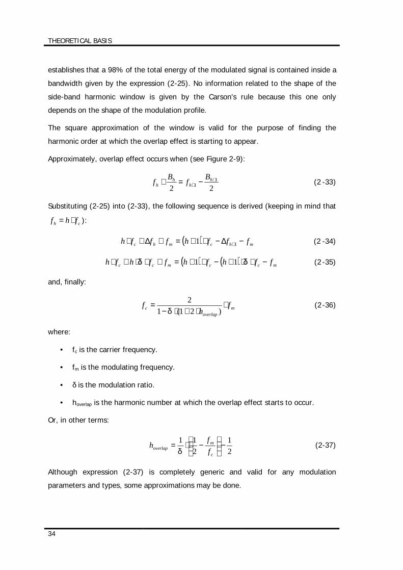
Approximately, overlap effect occurs when (see Figure 2-9):
221
1+
+ −=+ hh
hh
BfBf (2 -33)
Substituting (2-25) into (2-33), the following sequence is derived (keeping in mind that
ch fhf ⋅= ):
( ) mhcmhc fffhfffh −∆−⋅+=+∆+⋅ +11 (2 -34)
( ) ( ) mccmcc ffhfhffhfh −⋅⋅+−⋅+=+⋅⋅+⋅ δδ 11 (2 -35)
and, finally:
moverlap
c fh
f ⋅⋅+⋅−
=)21(1
2δ
(2-36)
where:
• fc is the carrier frequency.
• fm is the modulating frequency.
• δ is the modulation ratio.
• hoverlap is the harmonic number at which the overlap effect starts to occur.
Or, in other terms:
21
211
−
−⋅=
c
moverlap f
fh
δ (2-37)
Although expression (2-37) is completely generic and valid for any modulation
parameters and types, some approximations may be done.

THEORETICAL BASIS
35
As it can be derived from (2-37), the smaller fc (or the larger fm and δ), the smaller
hoverlap is to be found, but not significant differences arise because fc is commonly much
larger than fm, then the expression (2-37) can also be written in the following way:
21
211
−
⋅≈
δoverlaph (2-38)
Moreover, the modulation ratio δ is usually small enough (for instance, not larger than
2.5% for clock systems) as to simplify the expression (2-38), obtaining the following
reduced equation:
δ⋅≈
21
overlaph (2-39)
In other words, larger values of frequency deviation (for a defined fc) are to produce
overlap at lower main harmonic numbers. Influence of modulating frequency fm in this
overlap effect is significantly smaller and, in a first step, is negligible.
2.2.3 Influence of the modulation profile parameters
Modulation profiles are of great importance in the final results when a modulation
process is present. They are mainly responsible for the shape of the resulting spectrum
after the modulation process, but they also influence the displacement of the central
frequency up- or down-wards respect to the original signal. The following points deal
with these important aspects in more detail.
2.2.3.1 Influence on the power converter output voltage of the
modulation profile
It is of great interest to find out the influence of modulation profiles on the output
voltage of the converter. In order to answer this question, a finer development is
carried out onwards.
As in a real power converter, a square waveform is being frequency-modulated
following a certain modulation profile (e.g., Figure 2-10(a)), which means that the
instantaneous frequency of the signal is changing constantly (Figure 2-10(b)).
However, a condition must be guaranteed: the initial and the final frequencies inside a
modulating signal period (Tm) must be exactly the same. This way, a new more
complicated signal appears, but showing a constant periodTm (Figure 2-10(b)) which
repeats indefinitely in time.
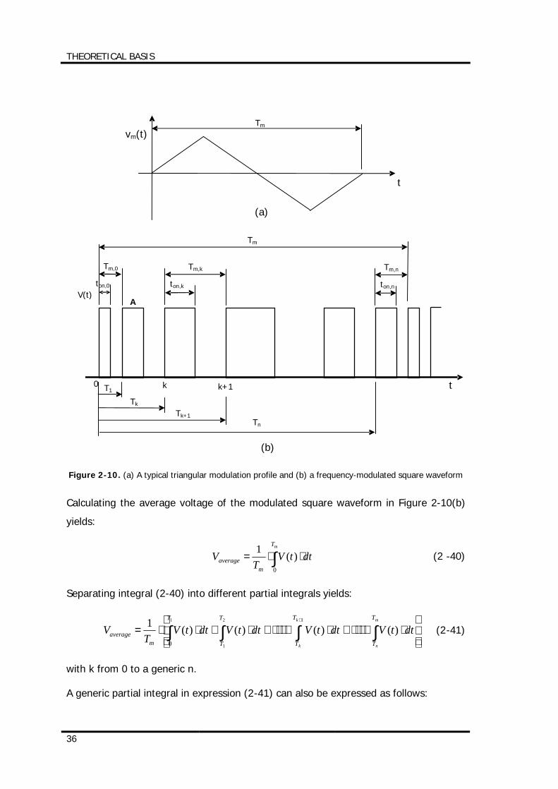
THEORETICAL BASIS
36
Figure 2-10. (a) A typical triangular modulation profile and (b) a frequency-modulated square waveform
Calculating the average voltage of the modulated square waveform in Figure 2-10(b)
yields:
∫ ⋅⋅=mT
maverage dttV
TV
0
)(1 (2 -40)
Separating integral (2-40) into different partial integrals yields:
⋅+⋅⋅⋅+⋅+⋅⋅⋅+⋅+⋅⋅= ∫ ∫∫∫
+12
1
1
)()()()(1
0
k
k
m
n
T
T
T
T
T
T
T
maverage dttVdttVdttVdttV
TV (2-41)
with k from 0 to a generic n.
A generic partial integral in expression (2-41) can also be expressed as follows:
ton,k
Tm,k
Tm
vm(t)
t
(a)
Tm
t
V(t) A
Tk
Tk+1
T1
(b)
Tn
k k+1 0
ton,0
Tm,0
ton,n
Tm,n
THEORETICAL BASIS
37
∫∫+
⋅=⋅+ kmk
k
k
k
TT
T
T
T
dttVdttV,1
)()( (2 -42)
But V(t) is zero outside the ton,k period, which yields:
kon
tT
T
tT
T
TT
T
T
T
tAdtAdtAdttVdttVkonk
k
konk
k
kmk
k
k
k
,
,,,1
)()( ⋅=⋅=⋅=⋅=⋅ ∫∫∫∫++++
(2-43)
Duty-cycle D is constant through the whole period Tm, that is, km
kon
Tt
D,
,= , thus the
generic partial integral in expression (2-43) can be rewritten as follows:
km
T
T
TDAdttVk
k
,
1
)( ⋅⋅=⋅∫+
(2-44)
Thus, expression (2-41) can take this more profitable aspect:
⋅⋅⋅= ∑
=
n
kkm
maverage TDA
TV
0,
1 (2 -45)
but the sum inside the integral is exactly the modulating period Tm; therefore a final
expression is derived:
[ ] DATDAT
V mm
average ⋅=⋅⋅⋅=1
(2 -46)
Therefore, no influence of the modulation profile on the output voltage is expected, at
least theoretically, with the condition of guaranteeing a constant instantaneous duty-
cycle D during the modulating period Tm.
2.2.3.2 Influence on the final spectrum of a voltage offset in the
modulation profile
For convenience, a modulating waveform can be expressed as a normalized profile
)(tvm instead of the nominal one (see Figure 2-11),
offsetmmm VtvVtv +⋅= )()( (2-57)
where Vm contains the actual amplitude of the modulation profile and Voffset is the
displacement of the whole modulation profile along with the vertical axis.
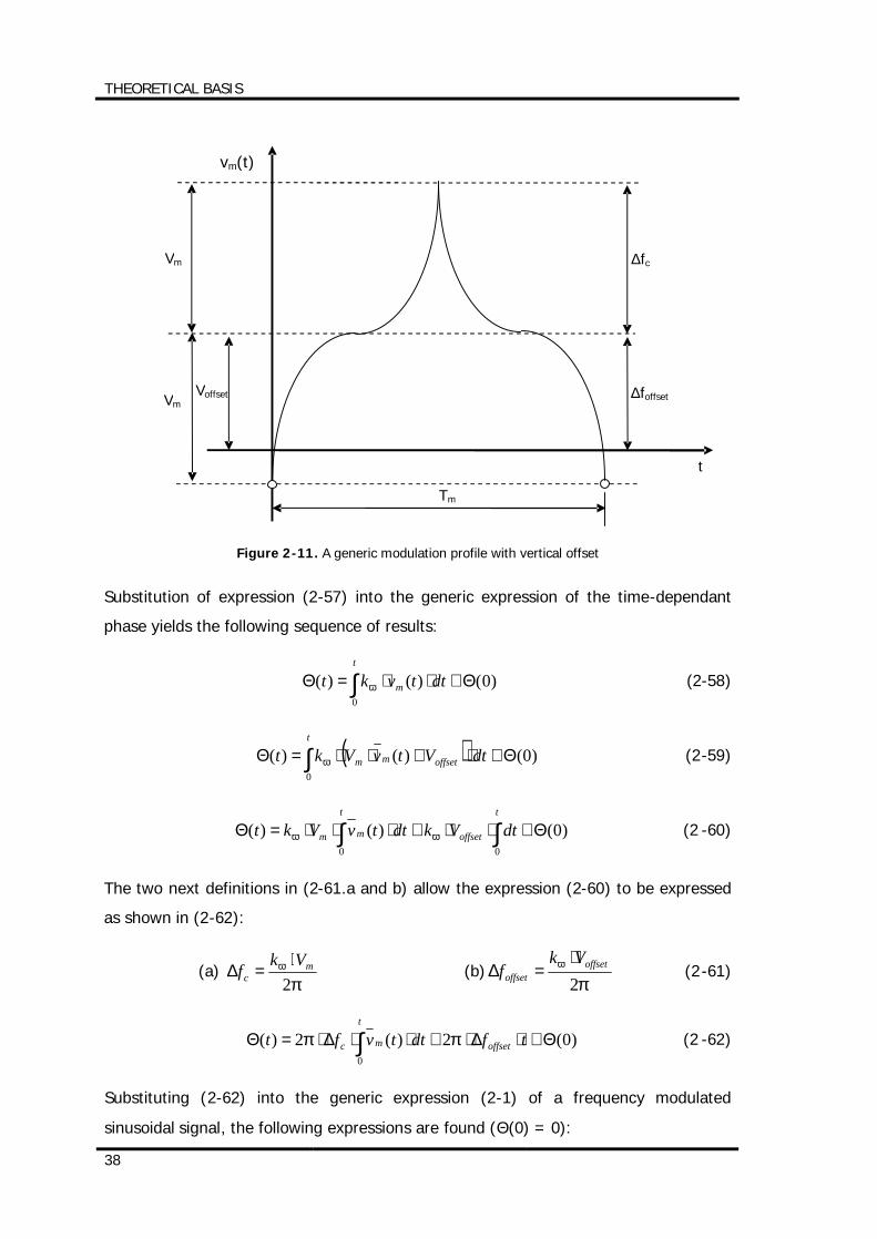
THEORETICAL BASIS
38
Figure 2-11. A generic modulation profile with vertical offset
Substitution of expression (2-57) into the generic expression of the time-dependant
phase yields the following sequence of results:
∫ Θ+⋅⋅=Θt
m dttvkt0
)0()()( ω (2-58)
( )∫ Θ+⋅+⋅⋅=Θt
offsetmm dtVtvVkt0
)0()()( ω (2-59)
∫ ∫ Θ+⋅⋅+⋅⋅⋅=Θt t
offsetmm dtVkdttvVkt0 0
)0()()( ωω (2 -60)
The two next definitions in (2-61.a and b) allow the expression (2-60) to be expressed
as shown in (2-62):
(a) π
ω
2m
cVkf ⋅
=∆ (b)π
ω
2offset
offset
Vkf
⋅=∆ (2-61)
∫ Θ+⋅∆⋅+⋅⋅∆⋅=Θt
offsetmc tfdttvft0
)0(2)(2)( ππ (2 -62)
Substituting (2-62) into the generic expression (2-1) of a frequency modulated
sinusoidal signal, the following expressions are found (Θ(0) = 0):
Vm
Vm Voffset
t
Tm
vm(t)
∆foffset
∆fc
THEORETICAL BASIS
39
( )
⋅⋅∆⋅+⋅∆⋅+⋅= ∫
t
mcoffsetc dttvftfAtF0
)(22cos)( ππω (2-63.1)
( )
⋅⋅⋅+⋅∆⋅+⋅= ∫
t
mmoffsetc dttvVktfAtF0
)(2cos)( ωπω (2-63)
In summary, it is a direct conclusion from (2-63) that a frequency offset (coming from
the modulation profile) does not produce any effects on the spectral components
resulting from a modulation process because they only depend on the modulation
profile characteristics )(tvm . But this feature gives the possibility of an easy generation
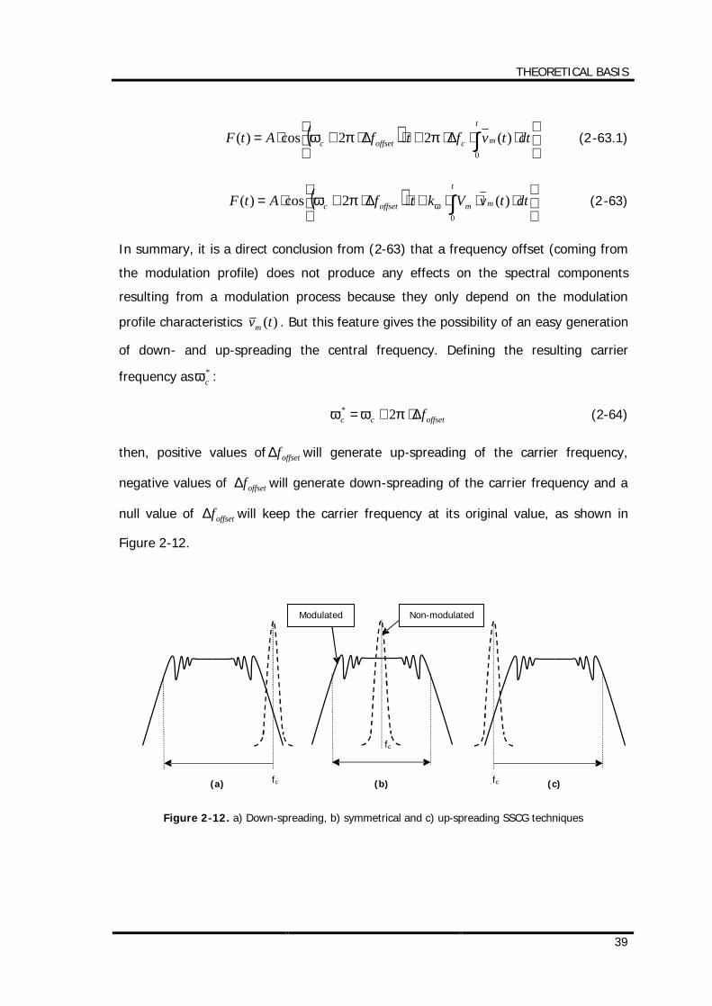
of down- and up-spreading the central frequency. Defining the resulting carrier
frequency as *cω :
offsetcc f∆⋅+= πωω 2* (2-64)
then, positive values of offsetf∆ will generate up-spreading of the carrier frequency,
negative values of offsetf∆ will generate down-spreading of the carrier frequency and a
null value of offsetf∆ will keep the carrier frequency at its original value, as shown in
Figure 2-12.
Figure 2-12. a) Down-spreading, b) symmetrical and c) up-spreading SSCG techniques
fc fc
fc
Non-modulated Modulated
(a) (b) (c)
THEORETICAL BASIS
40
2.2.3.3 Influence of the modulation profile phase-shift on the
spectrum resulting from the modulation process
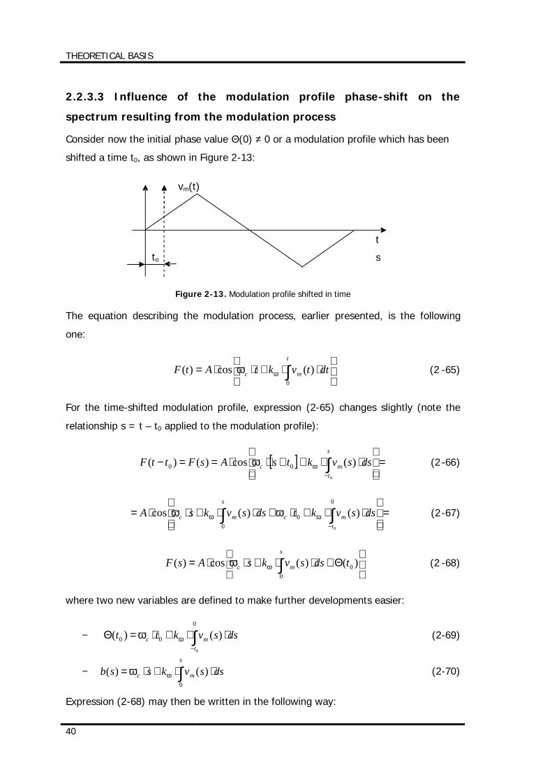
Consider now the initial phase value Θ(0) ≠ 0 or a modulation profile which has been
shifted a time t0, as shown in Figure 2-13:
Figure 2-13. Modulation profile shifted in time
The equation describing the modulation process, earlier presented, is the following
one:
⋅⋅+⋅⋅= ∫
t
mc dttvktAtF0
)(cos)( ωω (2 -65)
For the time-shifted modulation profile, expression (2-65) changes slightly (note the
relationship s = t – t0 applied to the modulation profile):
[ ] =
⋅⋅++⋅⋅==− ∫
−
s
tmc dssvktsAsFttF
0
)(cos)()( 00 ωω (2-66)
=
⋅⋅+⋅+⋅⋅+⋅⋅= ∫∫
−
0
00 0
)()(cost
mc
s
mc dssvktdssvksA ωω ωω (2-67)
Θ+⋅⋅+⋅⋅= ∫ )()(cos)( 0
0
tdssvksAsFs
mc ωω (2 -68)
where two new variables are defined to make further developments easier:
− ∫−
⋅⋅+⋅=Θ0
00
0
)()(t
mc dssvktt ωω (2-69)
− ∫ ⋅⋅+⋅=s
mc dssvkssb0
)()( ωω (2-70)
Expression (2-68) may then be written in the following way:
to
vm(t)
t
s
THEORETICAL BASIS
41
[ ])()(cos)( 0tsbAsF Θ+⋅= (2 -71)
Defining HSHIFT(f) as the Fourier transform (see Annex 3) of the time-shifted waveform
and HORI(f) as the original Fourier transform, then:
∫+∞
∞−
⋅⋅⋅− =⋅⋅−= dtettFfH tfjSHIFT
π20 )()( (2 -72)
∫∫+∞
∞−
⋅⋅⋅−⋅⋅⋅−+∞
∞−
+⋅⋅⋅− =⋅⋅⋅=⋅⋅= dsesFedsesF sfjtfjtsfj πππ 22)(2 )()( 00 (2 -73)
)()( 02 fHefH ORItfj
SHIFT ⋅= ⋅⋅⋅− π (2-74)
In summary, expression (2-74) shows that a phase shift in the modulation profile does
not change the harmonic amplitudes but the harmonic phases. In other words, spectral
power distribution of a frequency modulated waveform is independent on the absolute
phase of the modulating waveform. As it is only of interest the magnitude of the
harmonics, no care must be taken respect to the modulation profile phase.
2.2.3.4 Influence of the frequency peak deviation ∆fc defined by the
modulation profile
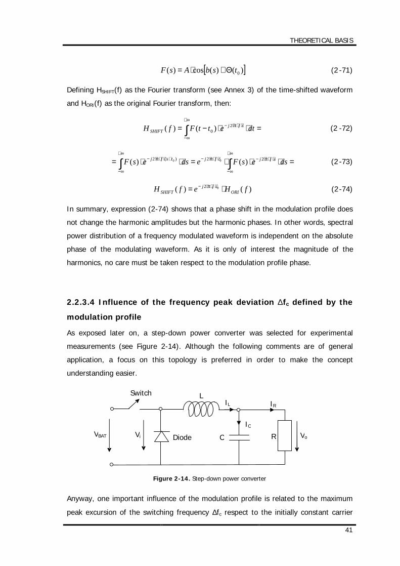
As exposed later on, a step-down power converter was selected for experimental
measurements (see Figure 2-14). Although the following comments are of general
application, a focus on this topology is preferred in order to make the concept
understanding easier.
Figure 2-14. Step-down power converter
Anyway, one important influence of the modulation profile is related to the maximum
peak excursion of the switching frequency ∆fc respect to the initially constant carrier
VBAT Vi Vo
L
C Diode
Switch
R
IL
IC
IR
THEORETICAL BASIS
42
frequency. As a general asseveration, a power converter consists of a low-pass filter
whose function is to filter out the whole ac components coming after the switch, thus
allowing only the dc component to flow across the load resistor. For a step-down
power converter, a LC filter is implemented. The cut-off frequency of this filter
establishes approximately the minimum high-frequency being rejected. For a constant
switching frequency, no problem is normally found and only the dc component flows
across the load resistor but, during the frequency modulation process, switching
frequency can fall beyond the cut-off frequency, then transmitting this low frequency
immediately to the load resistor, making the output voltage Vo oscillate, which is
unacceptable.
For the following analysis of converter in Figure 2-14, phasorial magnitudes are to be
considered:
→→→
⋅⋅⋅=− Loi ILjVV ω (2 -52)
RVII o
CL
→→→
+= (2 -53)
→→
⋅⋅⋅
= Co ICj
Vω1
(2 -54)
From the previous equations, the following gain is obtained:
RLjCLV
V
i
o
⋅⋅+⋅⋅−=→
→
ωω 21
1 (2 -55)
It is only of interest the module of these phasorial magnitudes, what it is obtained by
extracting the module of the previous expression, yielding the following relationship:
( )2
221
1
⋅+⋅⋅−
=
RLCL
VV
i
o
ωω
(2 -56)
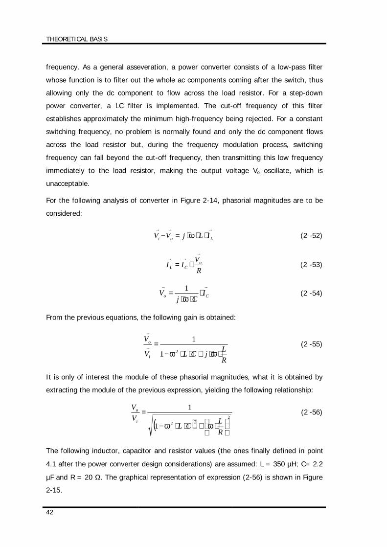
The following inductor, capacitor and resistor values (the ones finally defined in point
4.1 after the power converter design considerations) are assumed: L = 350 µH; C= 2.2
µF and R = 20 Ω. The graphical representation of expression (2-56) is shown in Figure
2-15.
THEORETICAL BASIS
43
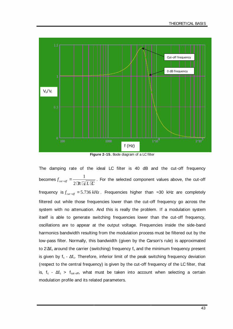
Figure 2-15. Bode diagram of a LC filter
The damping rate of the ideal LC filter is 40 dB and the cut-off frequency
becomesCL
f offcut⋅⋅⋅
=−π2
1. For the selected component values above, the cut-off
frequency is kHzf offcut 736.5=− . Frequencies higher than ≈30 kHz are completely
filtered out while those frequencies lower than the cut-off frequency go across the
system with no attenuation. And this is really the problem. If a modulation system
itself is able to generate switching frequencies lower than the cut-off frequency,
oscillations are to appear at the output voltage. Frequencies inside the side-band
harmonics bandwidth resulting from the modulation process must be filtered out by the
low-pass filter. Normally, this bandwidth (given by the Carson's rule) is approximated
to 2⋅∆fc around the carrier (switching) frequency fc and the minimum frequency present
is given by fc - ∆fc. Therefore, inferior limit of the peak switching frequency deviation
(respect to the central frequency) is given by the cut-off frequency of the LC filter, that
is, fc - ∆fc > fcut-off, what must be taken into account when selecting a certain
modulation profile and its related parameters.
Vo/Vi
f (Hz)
Cut-off frequency
0 dB frequency
THEORETICAL BASIS
44
2.2.3.5 Influence of a modulation profile with a certain average value
Another point of interest is related to the symmetrical aspect of the modulating
waveform )(tvm . If the modulation profile )(tvm is an odd function, a symmetrical side-
band harmonics distribution is expected (for instance, as in Figure 2-12). But what
happens when )(tvm is not an odd function thus giving an average value of )(tvm ≠ 0
during the modulating period Tm? It is clear that the final aspect of the side-band
harmonics can take whichever distribution depending on the shape of the modulating
waveform because it is this last which establishes the final shape of the side-band
harmonics. But which average frequency, equivalent to a constant switching frequency,
is to be found when the average value of the modulating waveform is not zero?
In frequency modulation, deviation δω(t) is supposed to be proportional to the
modulating signal voltage vm(t), that is:
)()()( tvktt mc ⋅=−= ωωωδω (2-57)
where kω is a sensitivity factor of the modulator expressed in rad/sec/V or Hz/V, ωc is
the carrier pulsation and ω(t) is the instantaneous pulsation. Instantaneous frequency
of the modulated signal is derived directly from expression (2-57), yielding the
following equation (2-58):
)(2
)( tvkftf mc ⋅⋅
+=π
ω (2 -58)
Once obtained the instantaneous frequency f(t), the instantaneous period T(t) is the
inverse of f(t), that is,
1)()( =⋅ tftT (2 -59)
The average value of instantaneous frequency f(t) is directly related to the average
value of the modulation profile, shown in expression (2-58). The relationship between
average frequency f and average period T is developed onwards:
∫ =⋅⋅=⋅mT
m
dttfT
TfT0
)(1 (2 -60)
Average periodT is a constant value which can be introduced into the integral:
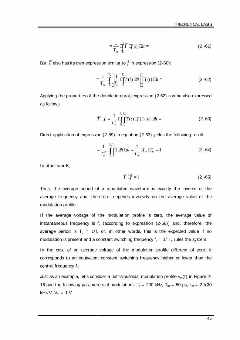
THEORETICAL BASIS
45
∫ =⋅⋅⋅=mT
m
dttfTT 0
)(1 (2 -61)
But T also has its own expression similar to f in expression (2-60):
∫ ∫ =⋅⋅
⋅⋅⋅=
m mT T
mm
dttfdttTTT 0 0
)()(11 (2 -62)
Applying the properties of the double integral, expression (2-62) can be also expressed
as follows:
∫ ∫ =⋅⋅⋅⋅=⋅m mT T
m
dtdttftTT
fT0 0
2 )()(1 (2 -63)
Direct application of expression (2-59) in equation (2-63) yields the following result:
11112
0 02 =⋅⋅=⋅⋅⋅= ∫ ∫ mm
m
T T
m
TTT
dtdtT
m m
(2 -64)
In other words,
1=⋅ fT (2 -65)
Thus, the average period of a modulated waveform is exactly the inverse of the
average frequency and, therefore, depends inversely on the average value of the
modulation profile.
If the average voltage of the modulation profile is zero, the average value of
instantaneous frequency is fc (according to expression (2-58)) and, therefore, the
average period is Tc = 1/fc or, in other words, this is the expected value if no
modulation is present and a constant switching frequency fc = 1/ Tc rules the system.
In the case of an average voltage of the modulation profile different of zero, it
corresponds to an equivalent constant switching frequency higher or lower than the
central frequency fc.
Just as an example, let's consider a half-sinusoidal modulation profile vm(t) in Figure 2-
16 and the following parameters of modulations: fc = 200 kHz, Tm = 50 µs, kω = 2⋅π⋅20
kHz/V, Vm = 1 V.
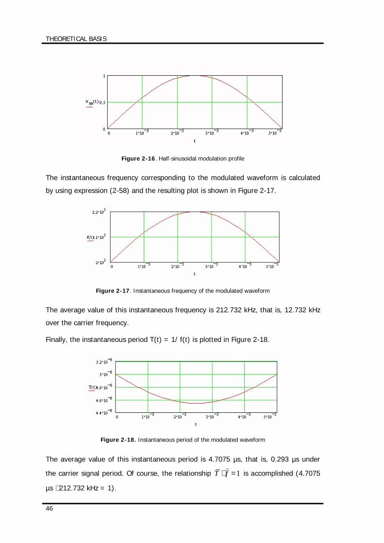
THEORETICAL BASIS
46
Figure 2-16. Half-sinusoidal modulation profile
The instantaneous frequency corresponding to the modulated waveform is calculated
by using expression (2-58) and the resulting plot is shown in Figure 2-17.
Figure 2-17. Instantaneous frequency of the modulated waveform
The average value of this instantaneous frequency is 212.732 kHz, that is, 12.732 kHz
over the carrier frequency.
Finally, the instantaneous period T(t) = 1/ f(t) is plotted in Figure 2-18.
Figure 2-18. Instantaneous period of the modulated waveform
The average value of this instantaneous period is 4.7075 µs, that is, 0.293 µs under
the carrier signal period. Of course, the relationship 1=⋅ fT is accomplished (4.7075
µs ⋅ 212.732 kHz = 1).
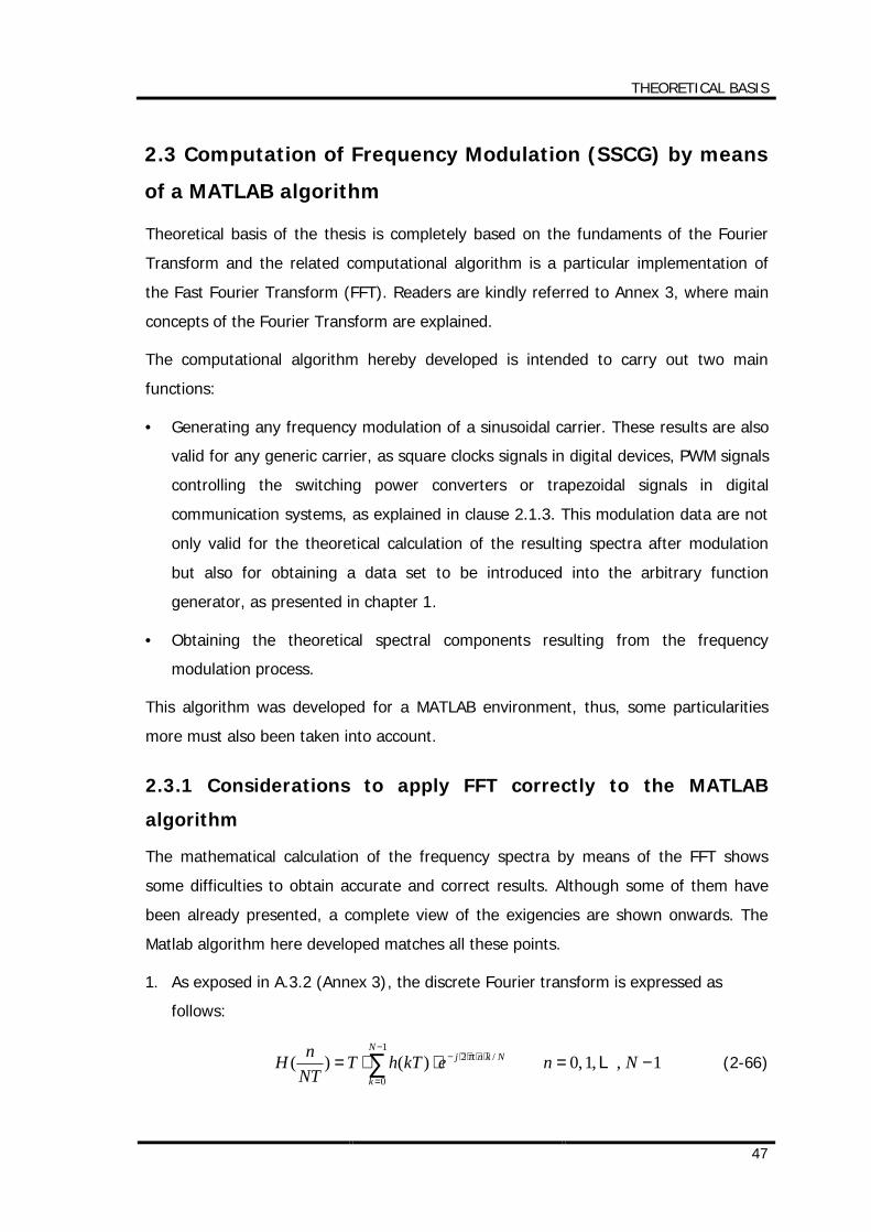
THEORETICAL BASIS
47
2.3 Computation of Frequency Modulation (SSCG) by means
of a MATLAB algorithm
Theoretical basis of the thesis is completely based on the fundaments of the Fourier
Transform and the related computational algorithm is a particular implementation of
the Fast Fourier Transform (FFT). Readers are kindly referred to Annex 3, where main
concepts of the Fourier Transform are explained.
The computational algorithm hereby developed is intended to carry out two main
functions:
• Generating any frequency modulation of a sinusoidal carrier. These results are also
valid for any generic carrier, as square clocks signals in digital devices, PWM signals
controlling the switching power converters or trapezoidal signals in digital
communication systems, as explained in clause 2.1.3. This modulation data are not
only valid for the theoretical calculation of the resulting spectra after modulation
but also for obtaining a data set to be introduced into the arbitrary function
generator, as presented in chapter 1.
• Obtaining the theoretical spectral components resulting from the frequency
modulation process.
This algorithm was developed for a MATLAB environment, thus, some particularities
more must also been taken into account.
2.3.1 Considerations to apply FFT correctly to the MATLAB
algorithm
The mathematical calculation of the frequency spectra by means of the FFT shows
some difficulties to obtain accurate and correct results. Although some of them have
been already presented, a complete view of the exigencies are shown onwards. The
Matlab algorithm here developed matches all these points.
1. As exposed in A.3.2 (Annex 3), the discrete Fourier transform is expressed as
follows:
1,,1,0)()(1
0
/2 −=⋅⋅= ∑−
=
⋅⋅⋅⋅− NnekThTNTnH
N
k
Nknj Lπ (2-66)
THEORETICAL BASIS
48
where T is the sampling period (time domain) and N is the number of equidistant
samples inside the truncation interval T0, equated to the modulating period
mm fT 1= .
The key-point of the discrete Fourier transform (DFT) (and, consequently, of the
FFT) is that the result matches exactly the one given by the continuous Fourier
transform just preserving the following conditions:
• The time function h(t) must be periodic.
• h(t) must be band-limited. An FM signal actually contains an infinite number
of side frequencies besides the carrier and therefore occupies infinite
bandwidth. However, the side frequencies quickly decrease in strength and
can be considered negligible at some point. In practice, a tradeoff between
bandwidth and distortion must be considered. The bandwidth of a
frequency modulated waveform is approximately given by the Carson’s rule.
• the sampling rate must be at least two times the largest frequency
component of h(t) è Nyquist's theorem.
• the truncation function x(t) must be non-zero over exactly one period (or
integer multiple period) of h(t).
DFT assumes that the waveform sampled during this sampling time of T (the
period of the signal) repeats itself down- and upwards indefinitely.
2. SSCG techniques are based on modulating the frequency of a carrier signal by
following a selected modulation profile. The waveform resulting from this
modulation process is a periodic signal whose frequency equates the frequency of
the modulating signal (fm), that is, the modulation profile. This is easy to
understand taking into account that the carrier signal frequency is constantly
varying, following the modulation profile, but showing the same value of frequency
(normally the carrier signal frequency) both at the beginning and at the end of the
complete cycle of variation through the modulation profile. This way, it is obtained
a modulated waveform which repeats itself indefinitely with a period of1/fm.
Expressed in equation form:
• Carrier signal è ( )tfFtF ccc ⋅⋅⋅⋅= π2sin)( 0
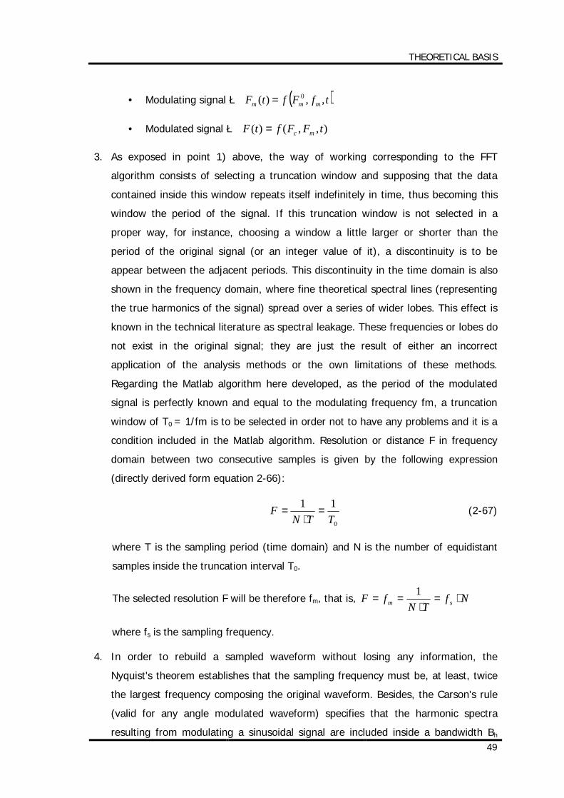
THEORETICAL BASIS
49
• Modulating signal è ( )tfFftF mmm ,,)( 0=
• Modulated signal è ),,()( tFFftF mc=
3. As exposed in point 1) above, the way of working corresponding to the FFT
algorithm consists of selecting a truncation window and supposing that the data
contained inside this window repeats itself indefinitely in time, thus becoming this
window the period of the signal. If this truncation window is not selected in a
proper way, for instance, choosing a window a little larger or shorter than the
period of the original signal (or an integer value of it), a discontinuity is to be
appear between the adjacent periods. This discontinuity in the time domain is also
shown in the frequency domain, where fine theoretical spectral lines (representing
the true harmonics of the signal) spread over a series of wider lobes. This effect is
known in the technical literature as spectral leakage. These frequencies or lobes do
not exist in the original signal; they are just the result of either an incorrect
application of the analysis methods or the own limitations of these methods.
Regarding the Matlab algorithm here developed, as the period of the modulated
signal is perfectly known and equal to the modulating frequency fm, a truncation
window of T0 = 1/fm is to be selected in order not to have any problems and it is a
condition included in the Matlab algorithm. Resolution or distance F in frequency
domain between two consecutive samples is given by the following expression
(directly derived form equation 2-66):
0
11TTN
F =⋅
= (2-67)
where T is the sampling period (time domain) and N is the number of equidistant
samples inside the truncation interval T0.
The selected resolution F will be therefore fm, that is, NfTN
fF sm ⋅=⋅
==1
where fs is the sampling frequency.
4. In order to rebuild a sampled waveform without losing any information, the
Nyquist's theorem establishes that the sampling frequency must be, at least, twice
the largest frequency composing the original waveform. Besides, the Carson's rule
(valid for any angle modulated waveform) specifies that the harmonic spectra
resulting from modulating a sinusoidal signal are included inside a bandwidth Bh
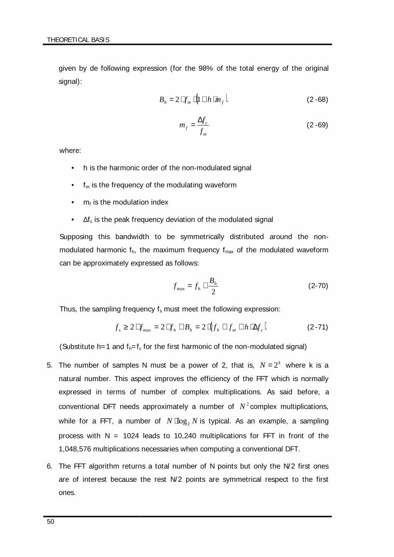
THEORETICAL BASIS
50
given by de following expression (for the 98% of the total energy of the original
signal):
( )fmh mhfB ⋅+⋅⋅= 12 (2 -68)
m
cf f
fm ∆= (2 -69)
where:
• h is the harmonic order of the non-modulated signal
• fm is the frequency of the modulating waveform
• mf is the modulation index
• ∆fc is the peak frequency deviation of the modulated signal
Supposing this bandwidth to be symmetrically distributed around the non-
modulated harmonic fh, the maximum frequency fmax of the modulated waveform
can be approximately expressed as follows:
2maxh
hBff += (2-70)
Thus, the sampling frequency fs must meet the following expression:
( )cmhhhs fhffBfff ∆⋅++⋅=+⋅=⋅≥ 222 max (2 -71)
(Substitute h=1 and fh=fc for the first harmonic of the non-modulated signal)
5. The number of samples N must be a power of 2, that is, kN 2= where k is a
natural number. This aspect improves the efficiency of the FFT which is normally
expressed in terms of number of complex multiplications. As said before, a
conventional DFT needs approximately a number of 2N complex multiplications,
while for a FFT, a number of NN 2log⋅ is typical. As an example, a sampling
process with N = 1024 leads to 10,240 multiplications for FFT in front of the
1,048,576 multiplications necessaries when computing a conventional DFT.
6. The FFT algorithm returns a total number of N points but only the N/2 first ones
are of interest because the rest N/2 points are symmetrical respect to the first
ones.
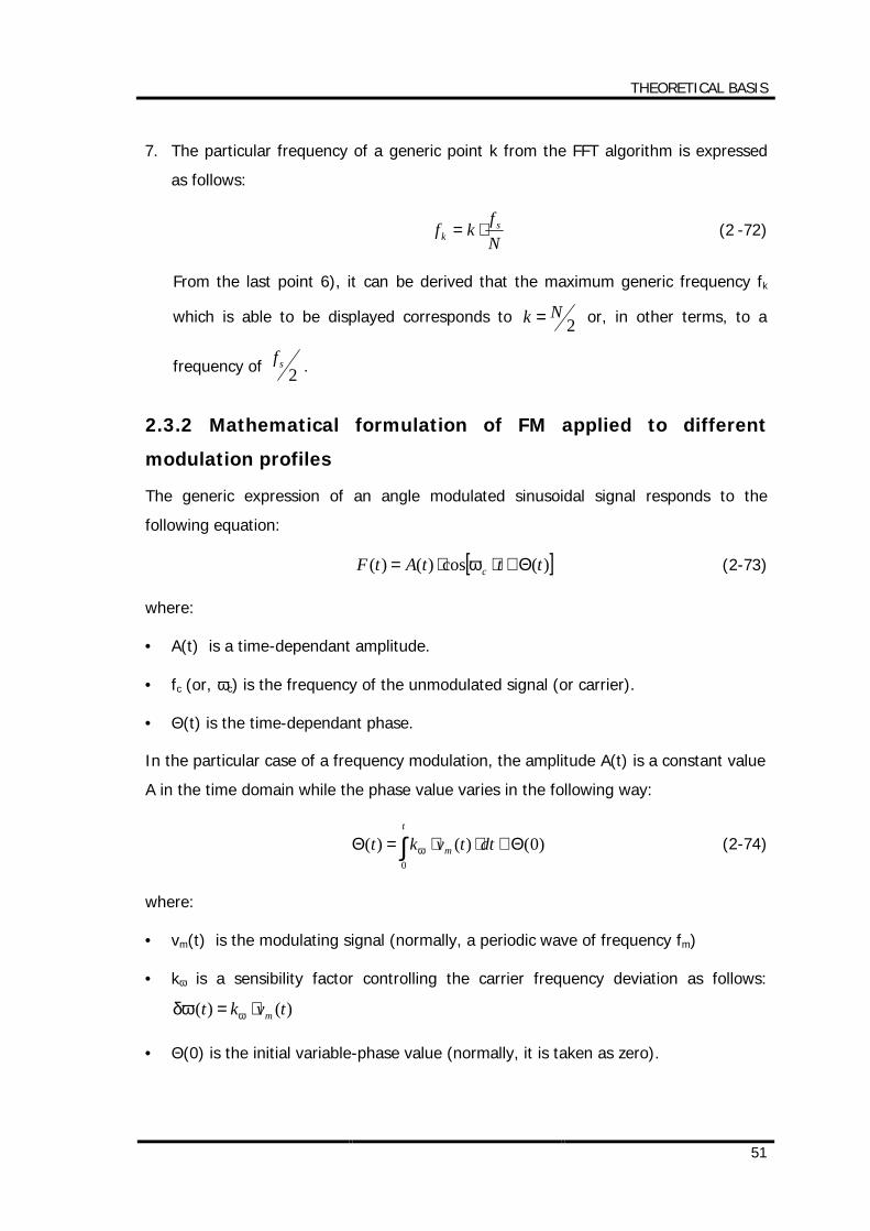
THEORETICAL BASIS
51
7. The particular frequency of a generic point k from the FFT algorithm is expressed
as follows:
Nfkf s
k ⋅= (2 -72)
From the last point 6), it can be derived that the maximum generic frequency fk
which is able to be displayed corresponds to 2Nk = or, in other terms, to a
frequency of 2sf .
2.3.2 Mathematical formulation of FM applied to different
modulation profiles
The generic expression of an angle modulated sinusoidal signal responds to the
following equation:
[ ])(cos)()( tttAtF c Θ+⋅⋅= ω (2-73)
where:
• A(t) is a time-dependant amplitude.
• fc (or, ωc) is the frequency of the unmodulated signal (or carrier).
• Θ(t) is the time-dependant phase.
In the particular case of a frequency modulation, the amplitude A(t) is a constant value
A in the time domain while the phase value varies in the following way:
∫ Θ+⋅⋅=Θt
m dttvkt0
)0()()( ω (2-74)
where:
• vm(t) is the modulating signal (normally, a periodic wave of frequency fm)
• kω is a sensibility factor controlling the carrier frequency deviation as follows:
)()( tvkt m⋅= ωδω
• Θ(0) is the initial variable-phase value (normally, it is taken as zero).

THEORETICAL BASIS
52
Thus, once the profile or modulating signal equation vm(t) is selected, its integration,
according to expression (2-74), yields a variable angle Θ(t) which, in summary,
produces the variation of the instantaneous carrier frequency
Two working hypotheses are of application in the whole further calculations:
• Θ(0) = 0. This particularity does not subtract any generality to the resulting
expression because it would only affect the absolute position of the window
generated by the modulation of the original carrier but not to the relative
distribution of the side-band harmonics inside this window (as demonstrated in
clause 2.2.3.3).
• Defining Vm as the peak value of the modulating signal vm(t), the product
mVk ⋅ω expresses the maximum peak deviation of the pulsation ω(t) respect to the
central pulsation ωc, that is:
ccm fVk ωπω ∆=∆⋅⋅=⋅ 2 (2-75)
2.3.2.1 Sinusoidal modulation profile
In this kind of modulation, the expression that rules this profile is:
)2()( tfsinVtv mmm ⋅⋅⋅⋅= π (2-76)
Applying the profile (2-76) into the equation (2-74), it is obtained:
∫ ⋅⋅=Θt
m dttvkt0
)()( ω (2-77)
∫ ⋅⋅⋅⋅⋅⋅=Θt
mm dttfsinVkt0
)2()( πω (2-78)
Integration of the equation (2-78) yields the following result:
( )[ ]tff
Vkt mm
m ⋅⋅⋅−⋅⋅⋅
⋅=Θ π
πω 2cos1
2)( (2-79)
Applying expression (2-75) into the equation (2-79), a more useful equation is to be
obtained:
( )[ ]tffft mm
c ⋅⋅⋅−⋅∆
=Θ π2cos1)( (2-80)
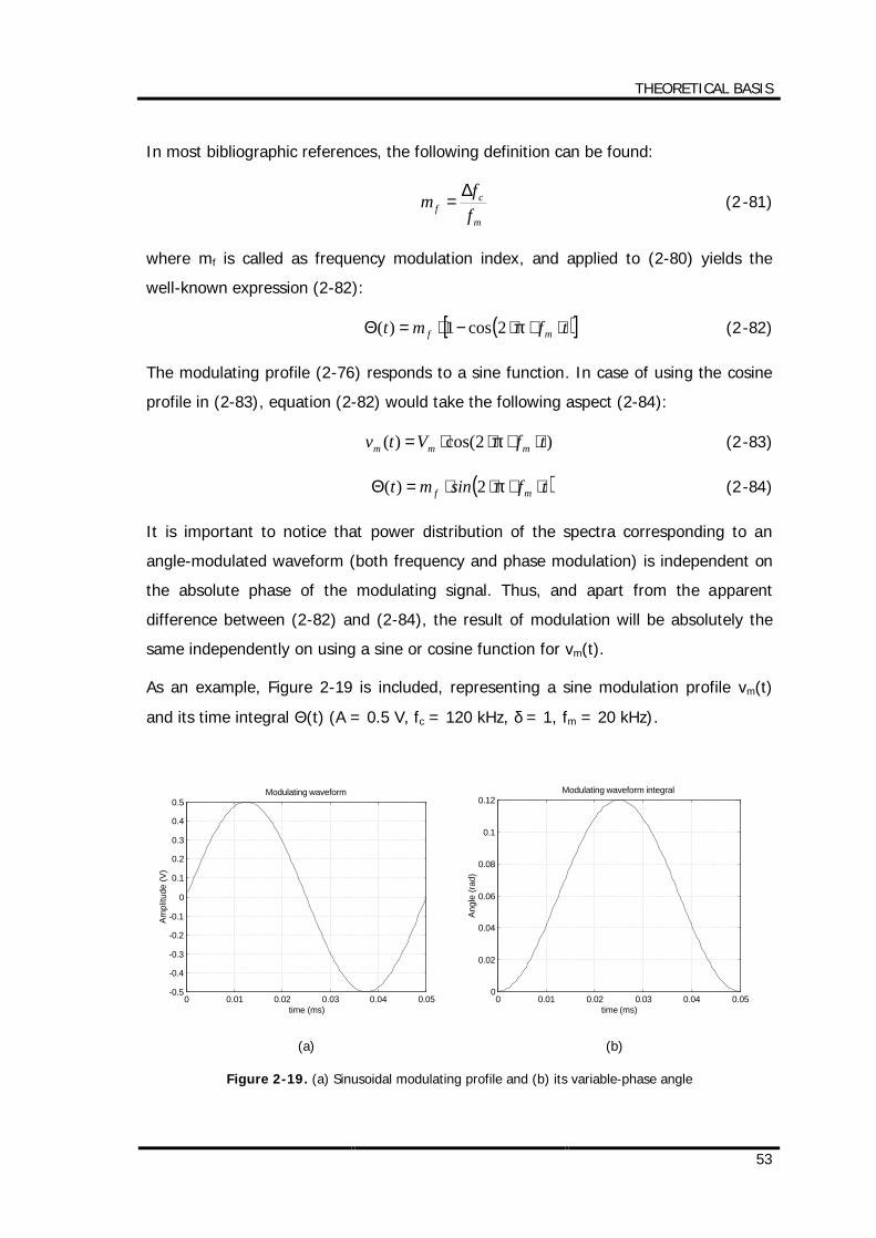
THEORETICAL BASIS
53
In most bibliographic references, the following definition can be found:
m
cf f
fm ∆= (2 -81)
where mf is called as frequency modulation index, and applied to (2-80) yields the
well-known expression (2-82):
( )[ ]tfmt mf ⋅⋅⋅−⋅=Θ π2cos1)( (2-82)
The modulating profile (2-76) responds to a sine function. In case of using the cosine
profile in (2-83), equation (2-82) would take the following aspect (2-84):
)2cos()( tfVtv mmm ⋅⋅⋅⋅= π (2-83)
( )tfsinmt mf ⋅⋅⋅⋅=Θ π2)( (2-84)
It is important to notice that power distribution of the spectra corresponding to an
angle-modulated waveform (both frequency and phase modulation) is independent on
the absolute phase of the modulating signal. Thus, and apart from the apparent
difference between (2-82) and (2-84), the result of modulation will be absolutely the
same independently on using a sine or cosine function for vm(t).
As an example, Figure 2-19 is included, representing a sine modulation profile vm(t)
and its time integral Θ(t) (A = 0.5 V, fc = 120 kHz, δ = 1, fm = 20 kHz).
0 0.01 0.02 0.03 0.04 0.05-0.5
-0.4
-0.3
-0.2
-0.1
0
0.1
0.2
0.3
0.4
0.5
time (ms)
Ampl
itude
(V)
Modulating waveform
0 0.01 0.02 0.03 0.04 0.050
0.02
0.04
0.06
0.08
0.1
0.12Modulating waveform integral
time (ms)
Angl
e (ra
d)
(a) (b)
Figure 2-19. (a) Sinusoidal modulating profile and (b) its variable-phase angle

THEORETICAL BASIS
54
2.3.2.2 Triangular modulation profile
The triangular modulation profile consists of three trams, each one defined by an
equation as shown below (Figure 2-20):
0 10 20 30 40 50-0.5
-0.4
-0.3
-0.2
-0.1
0
0.1
0.2
0.3
0.4
0.5
time (us)
Ampl
itude
(V)
Modulating waveform: triangular, s = 0.5
0 10 20 30 40 50
-0.5
-0.4
-0.3
-0.2
-0.1
0
0.1
0.2
0.3
0.4
0.5
time (us)
Ampl
itude
(V)
Modulating waveform: triangular, s = 0.25
(a) (b)
Figure 2-20. (a) Triangular modulating profiles: (a) symmetrical and (b) sawtooth type
Parameter s controls the position of the vertex of the triangular waveform from 0 to
Tm/2, thus making the implementation of profiles such a sawtooth waveform very easy.
Parameter s can range from 0 to 1, and, for a classical triangular profile, s = 0.5.
TRAM 1: Valid for t where 2
0 mTst ⋅<≤
The expression for the modulating profile along this tram 1 is:
ts
fVtv mmm ⋅⋅⋅=2)( (2 -85)
Applying the profile (2-85) to the equation (2-74) and making the integration, the
following result is obtained:
2)1( 2)( tsfft m
c ⋅⋅∆⋅⋅=Θ π (2 -86)
TRAM 2: Valid for t where mm TstTs ⋅
−<≤⋅
21
2
1
2 3
mTs⋅
2
mTs ⋅− )1( mTs⋅
2

THEORETICAL BASIS
55
Again, the expression for the modulating profile along this tram 2 is:
)21()1(
)( tfs
Vtv mm
m ⋅⋅−⋅−
= (2 -87)
Just for convenience, equation (2-74) is presented in such a way that it also reflects
the previous trams:
∫ ⋅⋅=Θt
m dttvkt0
)()( ω (2-88)
∫∫⋅
⋅
⋅⋅+⋅⋅=Θt
Tsm
Ts
m
m
m
dttvkdttvkt2
2
0
)()()( ωω (2-89)
or, in other terms:
∫⋅
⋅⋅+
⋅Θ=Θ
t
Tsm
m
m
dttvkTst2
)1( )(2
)( ω (2-90)
Resolving the integral in (2-90), the following result is obtained:
−⋅
⋅++⋅−⋅
−⋅∆⋅⋅+
⋅Θ=Θ 1
22)1(12
2)( 2)1()2( s
fsttf
sf
Tst
mmc
m π (2-91)
TRAM 3: Valid for t where mm TtTs<≤⋅
−
21
Finally, the expression for the modulating profile along this tram 3 is:
( )12)( −⋅⋅⋅= tfVs
tv mmm (2-92)
As in (2-89) and after integration, the expression of the variable-phase angle is as
follows:
[ ]( )
⋅
−+⋅−⋅⋅⋅∆⋅⋅+⋅−Θ=Θ
mmcm f
sttfs
fTst 12
121221)(2
2)2()3( π (2-93)
As an example, integrals Θ(t) (A = 0.5 V, fc = 120 kHz, δ = 1, fm = 20 kHz) are
included in Figure 2-21, corresponding to the triangular profiles in Figure 2-20.
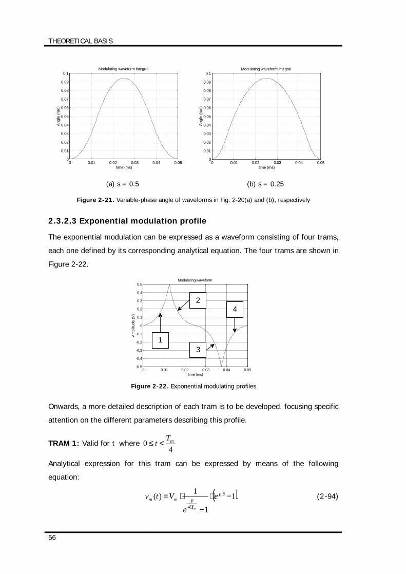
THEORETICAL BASIS
56
0 0.01 0.02 0.03 0.04 0.050
0.01
0.02
0.03
0.04
0.05
0.06
0.07
0.08
0.09
0.1Modulating waveform integral
time (ms)
Angl
e (ra
d)
0 0.01 0.02 0.03 0.04 0.05
0
0.01
0.02
0.03
0.04
0.05
0.06
0.07
0.08
0.09
0.1Modulating waveform integral
time (ms)
Angl
e (ra
d)
(a) s = 0.5 (b) s = 0.25
Figure 2-21. Variable-phase angle of waveforms in Fig. 2-20(a) and (b), respectively
2.3.2.3 Exponential modulation profile
The exponential modulation can be expressed as a waveform consisting of four trams,
each one defined by its corresponding analytical equation. The four trams are shown in
Figure 2-22.
0 0.01 0.02 0.03 0.04 0.05-0.5
-0.4
-0.3
-0.2
-0.1
0
0.1
0.2
0.3
0.4
0.5
time (ms)
Ampl
itude
(V)
Modulating waveform
Figure 2-22. Exponential modulating profiles
Onwards, a more detailed description of each tram is to be developed, focusing specific
attention on the different parameters describing this profile.
TRAM 1: Valid for t where 4
0 mTt <≤
Analytical expression for this tram can be expressed by means of the following
equation:
( )11
1)(4
−⋅
−
⋅= ⋅
⋅
tp
fpmm e
eVtv
m
(2-94)
1 3
4 2
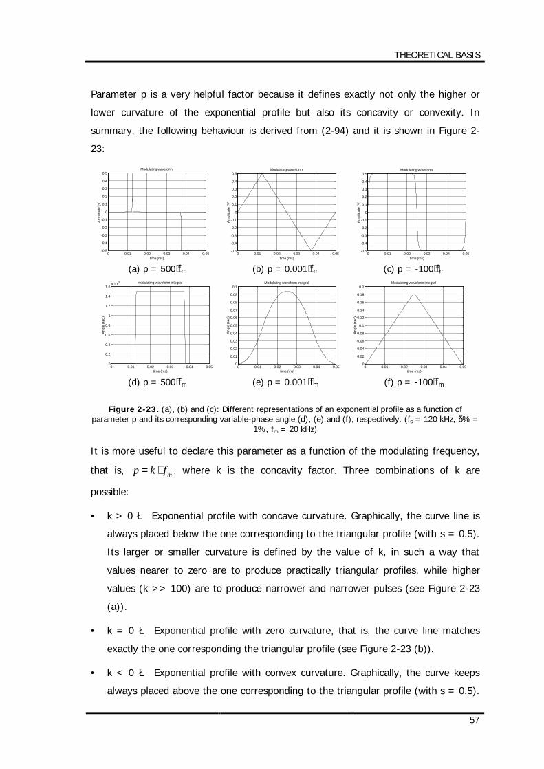
THEORETICAL BASIS
57
Parameter p is a very helpful factor because it defines exactly not only the higher or
lower curvature of the exponential profile but also its concavity or convexity. In
summary, the following behaviour is derived from (2-94) and it is shown in Figure 2-
23:
0 0.01 0.02 0.03 0.04 0.05-0.5
-0.4
-0.3
-0.2
-0.1
0
0.1
0.2
0.3
0.4
0.5
time (ms)
Ampl
itude
(V)
Modulating waveform
0 0.01 0.02 0.03 0.04 0.05
-0.5
-0.4
-0.3
-0.2
-0.1
0
0.1
0.2
0.3
0.4
0.5
time (ms)
Ampl
itude
(V)
Modulating waveform
0 0.01 0.02 0.03 0.04 0.05
-0.5
-0.4
-0.3
-0.2
-0.1
0
0.1
0.2
0.3
0.4
0.5
time (ms)
Am
plitu
de (V
)
Modulating waveform
(a) p = 500⋅fm (b) p = 0.001⋅fm (c) p = -100⋅fm
0 0.01 0.02 0.03 0.04 0.050
0.2
0.4
0.6
0.8
1
1.2
1.4
1.6x 10 -3 Modulating waveform integral
time (ms)
Angl
e (ra
d)
0 0.01 0.02 0.03 0.04 0.050
0.01
0.02
0.03
0.04
0.05
0.06
0.07
0.08
0.09
0.1Modulating waveform integral
time (ms)
Ang
le (r
ad)
0 0.01 0.02 0.03 0.04 0.050
0.02
0.04
0.06
0.08
0.1
0.12
0.14
0.16
0.18
0.2Modulating waveform integral
time (ms)
Ang
le (r
ad)
(d) p = 500⋅fm (e) p = 0.001⋅fm (f) p = -100⋅fm
Figure 2-23. (a), (b) and (c): Different representations of an exponential profile as a function of parameter p and its corresponding variable-phase angle (d), (e) and (f), respectively. (fc = 120 kHz, δ% =
1%, fm = 20 kHz)
It is more useful to declare this parameter as a function of the modulating frequency,
that is, mfkp ⋅= , where k is the concavity factor. Three combinations of k are
possible:
• k > 0 è Exponential profile with concave curvature. Graphically, the curve line is
always placed below the one corresponding to the triangular profile (with s = 0.5).
Its larger or smaller curvature is defined by the value of k, in such a way that
values nearer to zero are to produce practically triangular profiles, while higher
values (k >> 100) are to produce narrower and narrower pulses (see Figure 2-23
(a)).
• k = 0 è Exponential profile with zero curvature, that is, the curve line matches
exactly the one corresponding the triangular profile (see Figure 2-23 (b)).
• k < 0 è Exponential profile with convex curvature. Graphically, the curve keeps
always placed above the one corresponding to the triangular profile (with s = 0.5).
THEORETICAL BASIS
58
In the same way as in k > 0, larger or smaller curvatures are defined by the value
k, where values nearer to zero are to produce again practically triangular profiles
and higher values (|k| >> 100) are to produce nearly rectangular profiles, as
shown in Figure 2-23 (c).
Substituting profile equation (2-94) into expression (2-74) and integrating yields the
following result
( )11
12)(4
)1( −⋅−⋅
−⋅
⋅∆⋅⋅=Θ ⋅
⋅
tpeep
ft tp
fpc
m
π (2 -95)
TRAM 2: Valid for t where 24mm TtT
<≤
The modulating profile equation corresponding to this tram 2 can be expressed as
follows:
−⋅
−
⋅= ⋅−⋅
⋅
11
1)( 2
4
tpfp
fpmm ee
eVtv m
m
(2 -96)
Again, making the integration of the modulating profile expressed in (2-96) following
the expression (2-74) and applying the separation of the total integral into two partial
ones (as it was done with the triangular profile), the following expression (2-99)
results:
∫ ⋅⋅=Θt
m dttvkt0
)()( ω (2 -97)
∫∫ ⋅⋅+⋅⋅=Θt
Tm
T
m
m
m
dttvkdttvkt4
4
0
)()()( ωω (2 -98)
⋅+⋅−+⋅−
−⋅
⋅∆⋅⋅+
Θ=Θ ⋅⋅⋅−
⋅ m
fp
fp
tp
fpc
m
fptpeee
epfTt mm
m4
1
124)( 42
4
)1()2( π
(2-99)
TRAM 3: Valid for t where 4
32
mm TtT⋅<≤
THEORETICAL BASIS
59
The modulating profile equation corresponding to this tram 3 can be expressed as
follows:
−⋅
−⋅= ⋅⋅
−
⋅
tpfp
fpmm ee
eVtv m
m
2
41
1
1)( (2-100)
Again, integrating the modulating profile expressed in (2-100) following the expression
(2-74) and applying the separation of the total integral into two partial ones, the
following expression (2-103) is obtained:
∫ ⋅⋅=Θt
m dttvkt0
)()( ω (2 -101)
∫∫ ⋅⋅+⋅⋅=Θt
Tm
T
m
m
m
dttvkdttvkt2
2
0
)()()( ωω (2 -102)
+⋅
−⋅+⋅−
−⋅
⋅∆⋅⋅+
Θ=Θ ⋅
−⋅
⋅
12
1
122)( 2
4
)2()3(
m
fp
tp
fpc
m
fptpee
epfTt m
m
π
(2-103)
TRAM 4: Valid for t where mm TtT
<≤⋅4
3
The modulating profile equation corresponding to this tram 4 can be expressed as
follows:
−⋅
−
⋅= ⋅−
⋅
tpfp
fpmm ee
eVtv m
m
11
1)(4
(2 -104)
As above, the integration of the modulating profile expressed in (2-104) following the
expression (2-74) and the separation of the total integral into two partial ones yields
the following expression (2-107):
∫ ⋅⋅=Θt
m dttvkt0
)()( ω (2 -105)
∫∫⋅
⋅
⋅⋅+⋅⋅=Θt
Tm
T
m
m
m
dttvkdttvkt43
43
0
)()()( ωω (2 -106)
THEORETICAL BASIS
60
⋅−⋅+−⋅
−⋅
⋅∆⋅⋅+
⋅Θ=Θ ⋅⋅−
⋅ m
fp
fp
tp
fpc
m
fptpeee
epfTt mm
m43
1
1243)( 4
4
)3()4( π
(2-107)
The final results of these time-varying angles are shown graphically in Figure 2-23 (d),
(e) and (f) corresponding to their respective modulating waveforms in Figure 2-23 (a),
(b) and (c) (carrier and modulating signal values are fc = 120 kHz, δ% = 1%, fm = 20
kHz).
2.3.2.4 Discrete modulation profile
Apart from those modulation profiles which are likely to be expressed in an analytical
way, as the previous sinusoidal, triangular and exponential waveforms, it is very
appreciated to have the possibility to test any modulating waveforms, even those
which are difficult, when not impossible, to be expressed into an equation.
Figure 2-24 shows a modulating waveform and the whole parameters defining the
discretization process. Although the waveform below represents a symmetrical profile,
expressions and conclusions hereby developed are of generic validity; the only
condition is that the modulation profile in Figure 2-24 must be a complete period of the
modulating signal.
Figure 2-24. Discretization of a modulation profile
Vm
Vm Voffset
t
NP⋅∆T= Tm
∆T
2
vm
vmi
0
1
2
3
i
i
∆foffset
∆fc
NP
THEORETICAL BASIS
61
Obviously, the discrete modulation profile will be a set of couples (vmi , i) resulting from
a sampling process. A more detailed description of these parameters comes below:
• NP is the total number of points or samples corresponding to a period Tm (or 1/fm)
of the modulating waveform vm(t).
• ∆T is the spacing in the time domain between two consecutive samples and
corresponds to the period of the sampling signal of frequency fs, that is, sf
T 1=∆ .
Another useful expression can be derived from the NP definition:
NPTT m=∆ (2 -108)
• The couple (vmi, i) represents the sampled value of the modulating profile [vmi] at
the time corresponding to i. Pay attention to the fact that i is not a time value but a
sample number, ranging from 0 to NP-1.
• Voffset, Vm è Voffset represents a reference position of the whole waveform referred
to the horizontal axis and it is normally used to generate down- or up-spreading
modulation techniques. Voffset is selected in such a way that the same signal
excursion down and upwards is obtained. For a symmetrical shifting of the carrier
frequency above and below, Voffset must be zero with Vm giving the maximum peak
deviation carrier frequency as follows (from clause 2.1.1.1):
)()( tvkt m⋅= ωδω (2 -109)
and then,
mc Vk ⋅=∆ ωω (2 -110)
As defined in clause 2.1.1.1, the time-varying angle Θ(t) is expressed as follows:
∫ ⋅⋅=Θt
m dttvkt0
)()( ω (2-111)
Expression (2-111) can be easily translated in order to accept a sampled waveform
(from Figure 2-24):
Tvkii
jmj ∆⋅⋅=Θ ∑
−
=
1
0
)( ω (2-112)
THEORETICAL BASIS
62
For convenience, a normalized profile miv is to be used instead of the nominal one,
offsetmimmi VvVv +⋅= (2-113)
where a symmetrical profile (Vm = Vm1 = Vm2) has been used. This mathematical
simplification resulting from applying a symmetrical profile does not eliminate the
generality of this discussion but makes the analytical expressions easier to understand.
Thus, substituting expression (2-113) into the equation (2-112) yields the following
result:
=∆⋅⋅+∆⋅⋅=Θ ∑∑−
=
−
=⋅ TVkTvVki
i
joffset
i
jmjm
1
0
1
0
)( ωω (2-114)
iTVkvTVk offset
i
jmjm ⋅∆⋅⋅+⋅∆⋅⋅= ∑
−
=ωω
1
0
(2-115)
In a similar way as in (2-110), these two relationships are obtained (see Figure 2-24):
(a) π
ω
2m
cVkf ⋅
=∆ (b)π
ω
2offset
offset
Vkf
⋅=∆ (2-116)
where:
• ∆fc is the frequency peak deviation respect to the Voffset level.
• ∆foffset is the constant frequency deviation related to the horizontal axis.
From expression (2-108) and substituting the relationships 2-116(a) and (b) into the
equation (2-115), a final expression is derived (m
m Tf 1= ):
iff
NPv
ff
NPi
m
offseti
jmj
m
c ⋅∆
⋅+⋅∆
⋅=Θ ∑−
=
ππ 22)(1
0
i = 0 … NP-1 (2-117)
Anyway, the total number of points NP describing the discrete modulation profile does
not have to match the total number of points N describing the modulated waveform.
Moreover, a normal situation can be summarized in an inequality: NP < N. This
situation must be taken into account at the time of writing the MATLAB algorithm.
As shown in Figure 2-25, several time-points corresponding to the sampling of the
modulated signal will have the same discrete modulation profile value, that is, time-
points between two consecutives samples of the discrete modulation profile i and i+1
will expose exactly the same value (of course, a linear interpolation between i and i+1
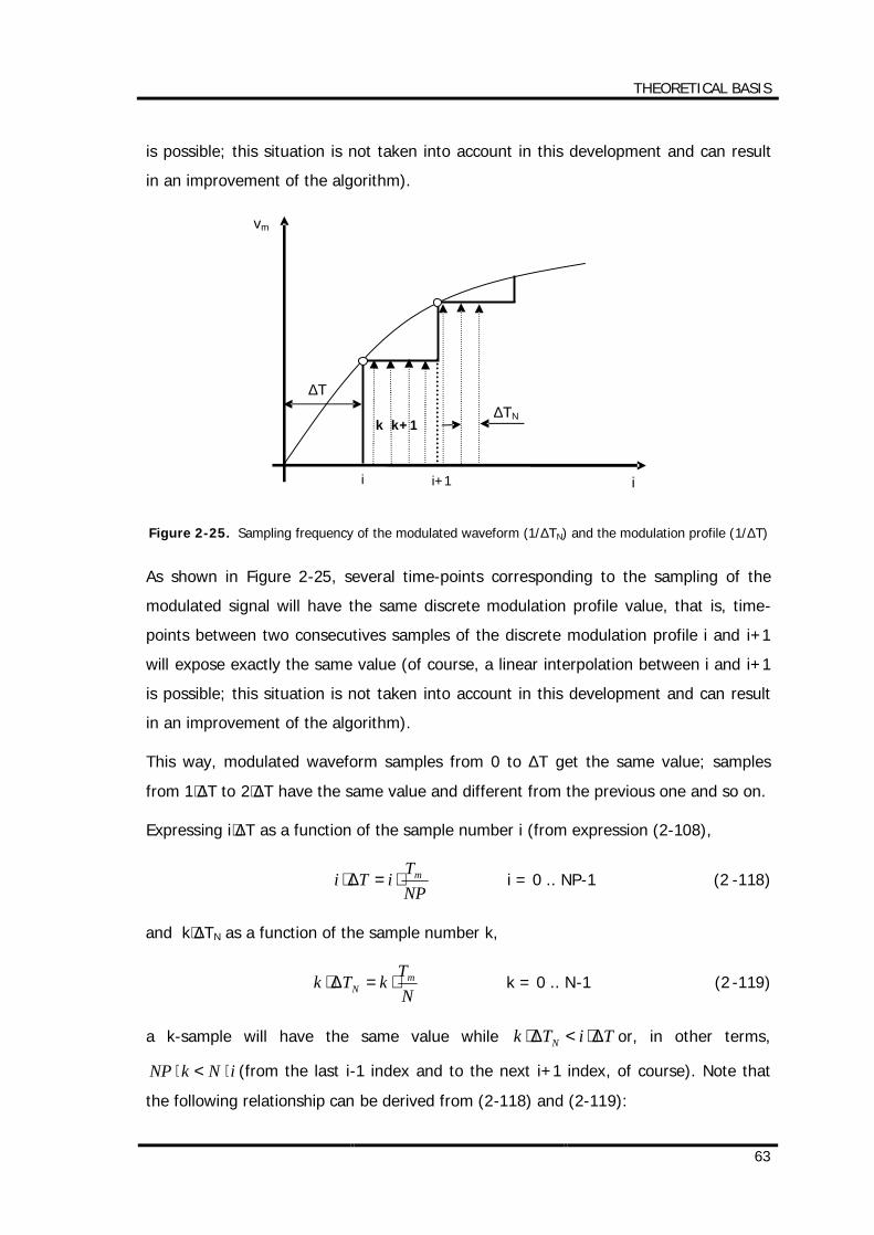
THEORETICAL BASIS
63
is possible; this situation is not taken into account in this development and can result
in an improvement of the algorithm).
Figure 2-25. Sampling frequency of the modulated waveform (1/∆TN) and the modulation profile (1/∆T)
As shown in Figure 2-25, several time-points corresponding to the sampling of the
modulated signal will have the same discrete modulation profile value, that is, time-
points between two consecutives samples of the discrete modulation profile i and i+1
will expose exactly the same value (of course, a linear interpolation between i and i+1
is possible; this situation is not taken into account in this development and can result
in an improvement of the algorithm).
This way, modulated waveform samples from 0 to ∆T get the same value; samples
from 1⋅∆T to 2⋅∆T have the same value and different from the previous one and so on.
Expressing i⋅∆T as a function of the sample number i (from expression (2-108),
NPTiTi m⋅=∆⋅ i = 0 .. NP-1 (2 -118)
and k⋅∆TN as a function of the sample number k,
NTkTk m
N ⋅=∆⋅ k = 0 .. N-1 (2 -119)
a k-sample will have the same value while TiTk N ∆⋅<∆⋅ or, in other terms,
iNkNP ⋅<⋅ (from the last i-1 index and to the next i+1 index, of course). Note that
the following relationship can be derived from (2-118) and (2-119):
∆TN
∆T
i
vm
i i+1
k k+1
THEORETICAL BASIS
64
mN TTNTNP =∆⋅=∆⋅ (2 -120)
Thus, k-samples between the i- and (i+1)-samples are to be calculated by following
this procedure (a Voffset = 0 was considered):
1. Let k = 0, i = 1, Θ(0) = 0, F(0) = 0
2. while NP⋅k < N⋅i, then
2.1. Let k=k+1
2.2. Calculation of F(k) [modulated waveform]
3. endwhile
4. if NP⋅k ≥ N⋅i, then
4.1. let i=i+1
4.2. Calculation of Θ(i) [new values only when increasing the i-index]
5. endif
6. Continue at point 2 till i=NP-1 (inclusive)
2.3.3 Structure of the algorithm
In order to make easier the readability of the MATLAB algorithm, an overview of its
internal structure was considered to be exposed. The following points make the
skeleton of this algorithm:
− First of all, a re-initialization of the environment is mandatory in order to avoid an
undesirable influence of previous calculations in the current one.
− Once the environment is ready, a complete list of definitions and parameters to be
used along this algorithm is to be done. Please keep in mind that Voffset = 0 is to be
considered in these computations, then simplifying the expressions obtained
previously. Main parameters hereby described are: switching (carrier) and
modulating frequencies (fc and fm), peak amplitudes of both signals (amp_c and
amp_m), parameter s for triangular modulation, percentage of modulation (delta),
initial values for modulating profile (vm=0) and phase value (theta = 0), peak
deviation of the carrier frequency (delta_fc), modulation index (mf), bandwidth of
the modulated waveform (bandwidth) from the Carson's rule and a final calculation
of the sampling frequency (fsampling).
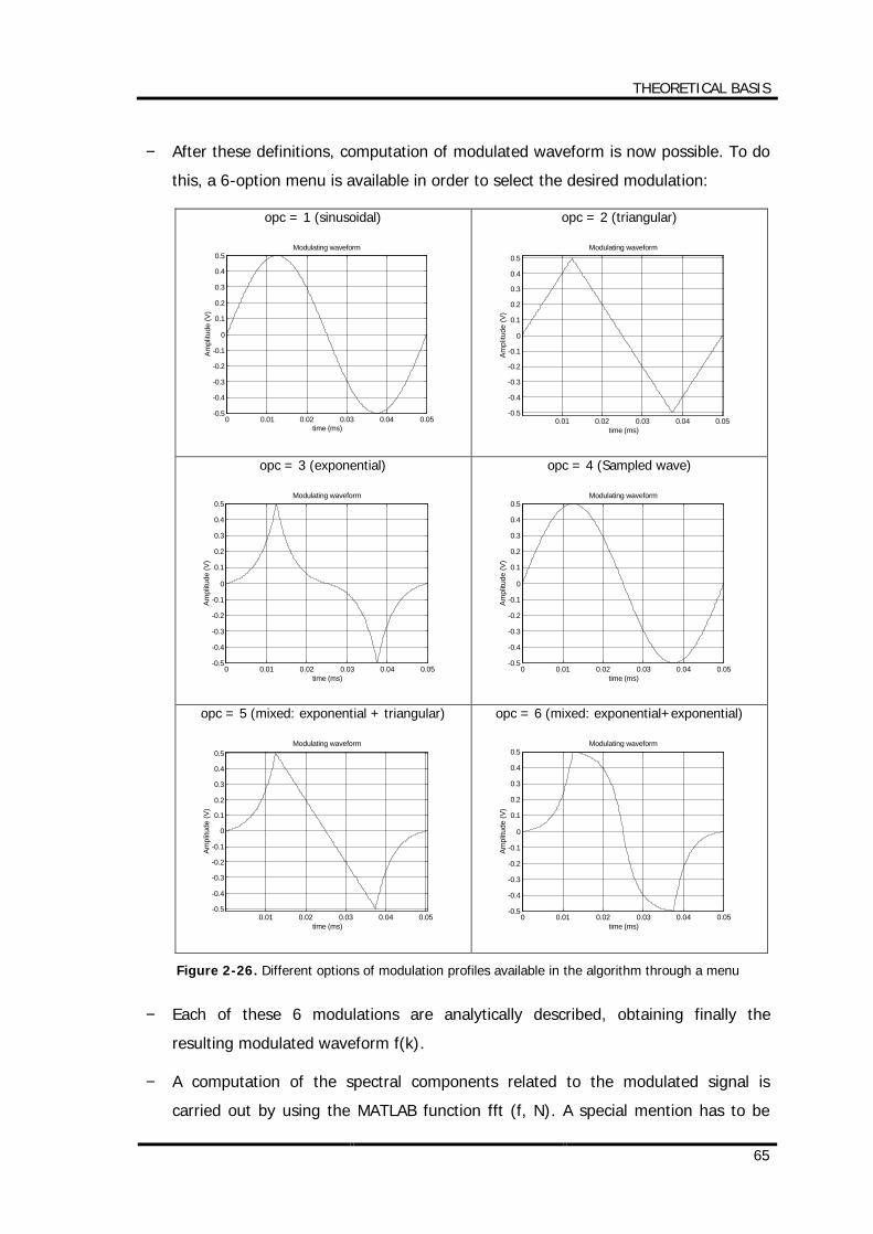
THEORETICAL BASIS
65
− After these definitions, computation of modulated waveform is now possible. To do
this, a 6-option menu is available in order to select the desired modulation:
opc = 1 (sinusoidal)
0 0.01 0.02 0.03 0.04 0.05-0.5
-0.4
-0.3
-0.2
-0.1
0
0.1
0.2
0.3
0.4
0.5
time (ms)
Ampl
itude
(V)
Modulating waveform
opc = 2 (triangular)
0.01 0.02 0.03 0.04 0.05-0.5
-0.4
-0.3
-0.2
-0.1
0
0.1
0.2
0.3
0.4
0.5
time (ms)
Ampl
itude
(V)
Modulating waveform
opc = 3 (exponential)
0 0.01 0.02 0.03 0.04 0.05-0.5
-0.4
-0.3
-0.2
-0.1
0
0.1
0.2
0.3
0.4
0.5
time (ms)
Ampl
itude
(V)
Modulating waveform
opc = 4 (Sampled wave)
0 0.01 0.02 0.03 0.04 0.05-0.5
-0.4
-0.3
-0.2
-0.1
0
0.1
0.2
0.3
0.4
0.5
time (ms)
Ampl
itude
(V)
Modulating waveform
opc = 5 (mixed: exponential + triangular)
0.01 0.02 0.03 0.04 0.05-0.5
-0.4
-0.3
-0.2
-0.1
0
0.1
0.2
0.3
0.4
0.5
time (ms)
Ampl
itude
(V)
Modulating waveform
opc = 6 (mixed: exponential+exponential)
0 0.01 0.02 0.03 0.04 0.05-0.5
-0.4
-0.3
-0.2
-0.1
0
0.1
0.2
0.3
0.4
0.5
time (ms)
Ampl
itude
(V)
Modulating waveform
Figure 2-26. Different options of modulation profiles available in the algorithm through a menu
− Each of these 6 modulations are analytically described, obtaining finally the
resulting modulated waveform f(k).
− A computation of the spectral components related to the modulated signal is
carried out by using the MATLAB function fft (f, N). A special mention has to be
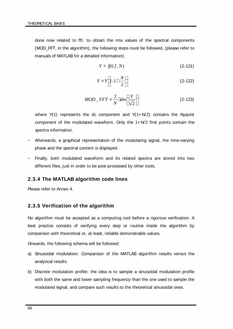
THEORETICAL BASIS
66
done now related to fft: to obtain the rms values of the spectral components
(MOD_FFT, in the algorithm), the following steps must be followed, (please refer to
manuals of MATLAB for a detailed information):
),( NffftY = (2-121)
+=
21:1 NYY (2-122)
⋅=
22_ YabsN
FFTMOD (2-123)
where Y(1) represents the dc component and Y(1+N/2) contains the Nyquist
component of the modulated waveform. Only the 1+N/2 first points contain the
spectra information.
− Afterwards, a graphical representation of the modulating signal, the time-varying
phase and the spectral content is displayed.
− Finally, both modulated waveform and its related spectra are stored into two
different files, just in order to be post-processed by other tools.
2.3.4 The MATLAB algorithm code lines
Please refer to Annex 4.
2.3.5 Verification of the algorithm
No algorithm must be accepted as a computing tool before a rigorous verification. A
best practice consists of verifying every step or routine inside the algorithm by
comparison with theoretical or, at least, reliable demonstrable values.
Onwards, the following schema will be followed:
a) Sinusoidal modulation: Comparison of the MATLAB algorithm results versus the
analytical results.
b) Discrete modulation profile: the idea is to sample a sinusoidal modulation profile
with both the same and lower sampling frequency than the one used to sample the
modulated signal, and compare such results to the theoretical sinusoidal ones.

THEORETICAL BASIS
67
c) Rest of modulation profiles: Unlike the sinusoidal modulation, no theoretical
expression for the spectral content of the modulated waveforms (mainly, regarding
to triangular and exponential modulations) is easy to derive because of its great
complexity. However, if the verification for an analytically described sinusoidal
modulation profile is properly accomplished, it makes sense to think that this is also
extensible to the rest of modulation profiles also expressed into an analytical form,
really the case of triangular and exponential profiles. Anyway, and in order to test
the equations in the MATLAB algorithm, a second verification will be made,
consisting of sampling these modulation profiles in order to use them as an input
for the discrete calculation at the MATLAB algorithm (opc=4 in point 2.3.3). These
results will be then compared to the ones obtained with several opc options (see
Figure 2-26), particularly, triangular and exponential modulation profiles.
There are some other modulation profiles (opc = 5, 6) available in the MATLAB
algorithm. They are usually just a combination of the first three ones, that is,
sinusoidal, triangular and exponential profiles. Because verification must be done
for these three profiles, further combination of them has not to be validated just
paying attention to the right writing of the equations describing the waveforms in
the algorithm.
In every case, the discrete modulation profile to be used must match the one
calculated by the MATLAB algorithm. Test discretized profiles can be obtained, for
instance, by means of commercial software like MathCad or MATLAB itself and they
must guarantee that the same modulation profile is running in the MATLAB algorithm.
a) Sinusoidal carrier modulated by a sinusoidal signal [RD-1]
First of all, theoretical development of this modulation is mandatory to derive.
The theoretical expression of a sinusoidal carrier modulated by another sinusoidal
waveform is usually expressed as follows:
[ ]tmtVtF mfcc ωω sincos)( +⋅= (2-124)
From a trigonometric equality
( ) ( )( )tmttmtVtF mfcmfcc ωωωω sinsinsinsincoscos)( ⋅−⋅⋅= (2-125)

THEORETICAL BASIS
68
In order to establish a relationship between ( )tm mf ωsincos and ( )tm mf ωsinsin , let
consider the function
tjm mfetg ωsin)( = (2-126)
Fourier's exponential series is represented by
∑∞
−∞=
⋅=n
tjnn ectg ω)( (2-127)
with
∫ −⋅=π ω ω
π
2
0)()(
21 tdetgc tjn
n (2-128)
The Bessel's function of first specie is defined by
∫ −⋅=π ωω ω
π
2
0
sin )(21)( tdeemJ tjntjm
fnmf (2-129)
which is similar to (2-128) with ωm replaced by ω and tjm mfetg ωsin)( = . Thus, the
following equalities can be exposed:
)( fnn mJc = (2-130)
∑∞
−∞=
⋅=n
tjnfn
memJtg ω)()( (2-131)
Adding the components +n and –n of g(t), it can be demonstrated that:
)()1()( fnn
fn mJmJ ⋅−=− (2-132)
Thus, for n even,
=⋅+⋅ −−
tjnfn
tjnfn
mm emJemJ ωω )()(
( )tjntjnfn
mm eemJ ωω −+⋅= )(
( )tnmJ mfn ⋅⋅⋅⋅= ωcos)(2 (2 -133)
For n odd,
=⋅+⋅ −−
tjnfn
tjnfn
mm emJemJ ωω )()(
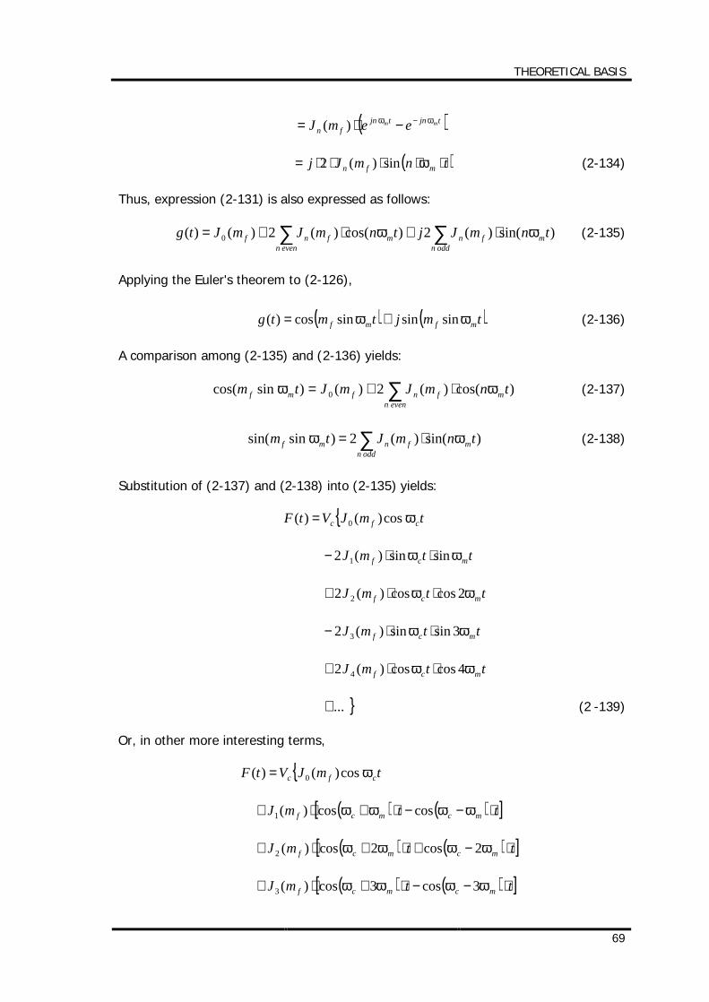
THEORETICAL BASIS
69
( )tjntjnfn
mm eemJ ωω −−⋅= )(
( )tnmJj mfn ⋅⋅⋅⋅⋅= ωsin)(2 (2-134)
Thus, expression (2-131) is also expressed as follows:
∑∑ ⋅+⋅+=oddn
mfnevenn
mfnf tnmJjtnmJmJtg )sin()(2)cos()(2)()( 0 ωω (2-135)
Applying the Euler's theorem to (2-126),
( ) ( )tmjtmtg mfmf ωω sinsinsincos)( += (2-136)
A comparison among (2-135) and (2-136) yields:
∑ ⋅+=evenn
mfnfmf tnmJmJtm )cos()(2)()sincos( 0 ωω (2-137)
∑ ⋅=oddn
mfnmf tnmJtm )sin()(2)sinsin( ωω (2-138)
Substitution of (2-137) and (2-138) into (2-135) yields:
tmJVtF cfc ωcos)()( 0=
ttmJ mcf ωω sinsin)(2 1 ⋅⋅−
ttmJ mcf ωω 2coscos)(2 2 ⋅⋅+
ttmJ mcf ωω 3sinsin)(2 3 ⋅⋅−
ttmJ mcf ωω 4coscos)(2 4 ⋅⋅+
...+ (2 -139)
Or, in other more interesting terms,
tmJVtF cfc ωcos)()( 0=
( ) ( )[ ]ttmJ mcmcf ⋅−−⋅+⋅+ ωωωω coscos)(1
( ) ( )[ ]ttmJ mcmcf ⋅−+⋅+⋅+ ωωωω 2cos2cos)(2
( ) ( )[ ]ttmJ mcmcf ⋅−−⋅+⋅+ ωωωω 3cos3cos)(3
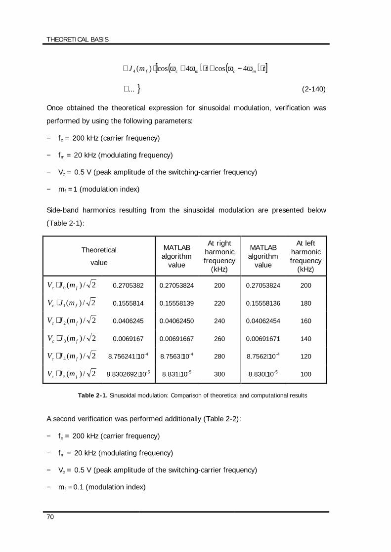
THEORETICAL BASIS
70
( ) ( )[ ]ttmJ mcmcf ⋅−+⋅+⋅+ ωωωω 4cos4cos)(4
...+ (2-140)
Once obtained the theoretical expression for sinusoidal modulation, verification was
performed by using the following parameters:
− fc = 200 kHz (carrier frequency)
− fm = 20 kHz (modulating frequency)
− Vc = 0.5 V (peak amplitude of the switching-carrier frequency)
− mf =1 (modulation index)
Side-band harmonics resulting from the sinusoidal modulation are presented below
(Table 2-1):
Theoretical
value
MATLAB algorithm
value
At right harmonic frequency
(kHz)
MATLAB algorithm
value
At left harmonic frequency
(kHz)
2/)(0 fc mJV ⋅ 0.2705382 0.27053824 200 0.27053824 200
2/)(1 fc mJV ⋅ 0.1555814 0.15558139 220 0.15558136 180
2/)(2 fc mJV ⋅ 0.0406245 0.04062450 240 0.04062454 160
2/)(3 fc mJV ⋅ 0.0069167 0.00691667 260 0.00691671 140
2/)(4 fc mJV ⋅ 8.756241⋅10-4 8.7563⋅10-4 280 8.7562⋅10-4 120
2/)(5 fc mJV ⋅ 8.8302692⋅10-5 8.831⋅10-5 300 8.830⋅10-5 100
Table 2-1. Sinusoidal modulation: Comparison of theoretical and computational results
A second verification was performed additionally (Table 2-2):
− fc = 200 kHz (carrier frequency)
− fm = 20 kHz (modulating frequency)
− Vc = 0.5 V (peak amplitude of the switching-carrier frequency)
− mf =0.1 (modulation index)
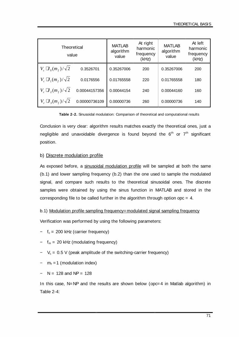
THEORETICAL BASIS
71
Theoretical
value
MATLAB algorithm
value
At right harmonic frequency
(kHz)
MATLAB algorithm
value
At left harmonic frequency
(kHz)
2/)(0 fc mJV ⋅ 0.3526701 0.35267006 200 0.35267006 200
2/)(1 fc mJV ⋅ 0.0176556 0.01765558 220 0.01765558 180
2/)(2 fc mJV ⋅ 0.00044157356 0.00044154 240 0.00044160 160
2/)(3 fc mJV ⋅ 0.00000736109 0.00000736 260 0.00000736 140
Table 2-2. Sinusoidal modulation: Comparison of theoretical and computational results
Conclusion is very clear: algorithm results matches exactly the theoretical ones, just a
negligible and unavoidable divergence is found beyond the 6th or 7th significant
position.
b) Discrete modulation profile
As exposed before, a sinusoidal modulation profile will be sampled at both the same
(b.1) and lower sampling frequency (b.2) than the one used to sample the modulated
signal, and compare such results to the theoretical sinusoidal ones. The discrete
samples were obtained by using the sinus function in MATLAB and stored in the
corresponding file to be called further in the algorithm through option opc = 4.
b.1) Modulation profile sampling frequency=modulated signal sampling frequency
Verification was performed by using the following parameters:
− fc = 200 kHz (carrier frequency)
− fm = 20 kHz (modulating frequency)
− Vc = 0.5 V (peak amplitude of the switching-carrier frequency)
− mf =1 (modulation index)
− N = 128 and NP = 128
In this case, N=NP and the results are shown below (opc=4 in Matlab algorithm) in
Table 2-4:
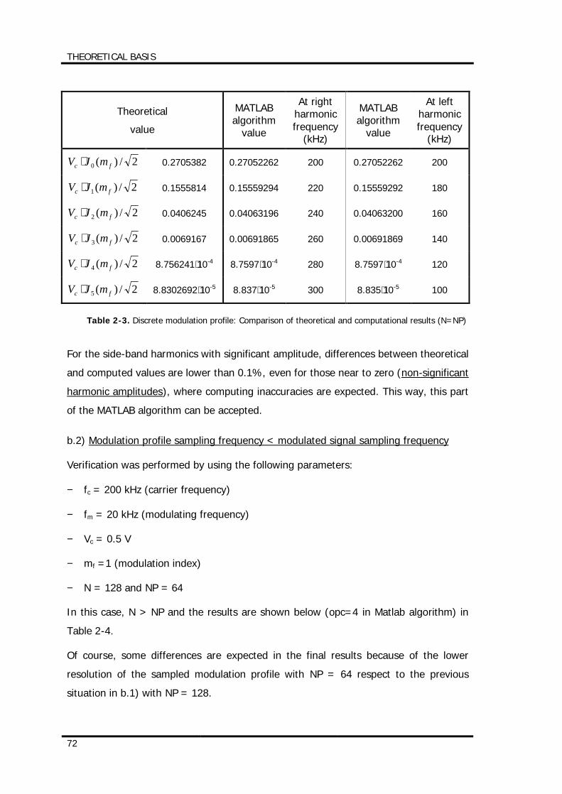
THEORETICAL BASIS
72
Theoretical
value
MATLAB algorithm
value
At right harmonic frequency
(kHz)
MATLAB algorithm
value
At left harmonic frequency
(kHz)
2/)(0 fc mJV ⋅ 0.2705382 0.27052262 200 0.27052262 200
2/)(1 fc mJV ⋅ 0.1555814 0.15559294 220 0.15559292 180
2/)(2 fc mJV ⋅ 0.0406245 0.04063196 240 0.04063200 160
2/)(3 fc mJV ⋅ 0.0069167 0.00691865 260 0.00691869 140
2/)(4 fc mJV ⋅ 8.756241⋅10-4 8.7597⋅10-4 280 8.7597⋅10-4 120
2/)(5 fc mJV ⋅ 8.8302692⋅10-5 8.837⋅10-5 300 8.835⋅10-5 100
Table 2-3. Discrete modulation profile: Comparison of theoretical and computational results (N=NP)
For the side-band harmonics with significant amplitude, differences between theoretical
and computed values are lower than 0.1%, even for those near to zero (non-significant
harmonic amplitudes), where computing inaccuracies are expected. This way, this part
of the MATLAB algorithm can be accepted.
b.2) Modulation profile sampling frequency < modulated signal sampling frequency
Verification was performed by using the following parameters:
− fc = 200 kHz (carrier frequency)
− fm = 20 kHz (modulating frequency)
− Vc = 0.5 V
− mf =1 (modulation index)
− N = 128 and NP = 64
In this case, N > NP and the results are shown below (opc=4 in Matlab algorithm) in
Table 2-4.
Of course, some differences are expected in the final results because of the lower
resolution of the sampled modulation profile with NP = 64 respect to the previous
situation in b.1) with NP = 128.
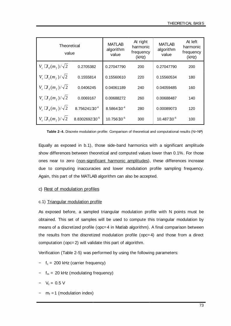
THEORETICAL BASIS
73
Theoretical
value
MATLAB algorithm
value
At right harmonic frequency
(kHz)
MATLAB algorithm
value
At left harmonic frequency
(kHz)
2/)(0 fc mJV ⋅ 0.2705382 0.27047790 200 0.27047790 200
2/)(1 fc mJV ⋅ 0.1555814 0.15560610 220 0.15560534 180
2/)(2 fc mJV ⋅ 0.0406245 0.04061189 240 0.04059485 160
2/)(3 fc mJV ⋅ 0.0069167 0.00688272 260 0.00688487 140
2/)(4 fc mJV ⋅ 8.756241⋅10-4 8.5864⋅10-4 280 0.00089073 120
2/)(5 fc mJV ⋅ 8.8302692⋅10-5 10.756⋅10-5 300 10.487⋅10-5 100
Table 2-4. Discrete modulation profile: Comparison of theoretical and computational results (N>NP)
Equally as exposed in b.1), those side-band harmonics with a significant amplitude
show differences between theoretical and computed values lower than 0.1%. For those
ones near to zero (non-significant harmonic amplitudes), these differences increase
due to computing inaccuracies and lower modulation profile sampling frequency.
Again, this part of the MATLAB algorithm can also be accepted.
c) Rest of modulation profiles
c.1) Triangular modulation profile
As exposed before, a sampled triangular modulation profile with N points must be
obtained. This set of samples will be used to compute this triangular modulation by
means of a discretized profile (opc=4 in Matlab algorithm). A final comparison between
the results from the discretized modulation profile (opc=4) and those from a direct
computation (opc=2) will validate this part of algorithm.
Verification (Table 2-5) was performed by using the following parameters:
− fc = 200 kHz (carrier frequency)
− fm = 20 kHz (modulating frequency)
− Vc = 0.5 V
− mf =1 (modulation index)
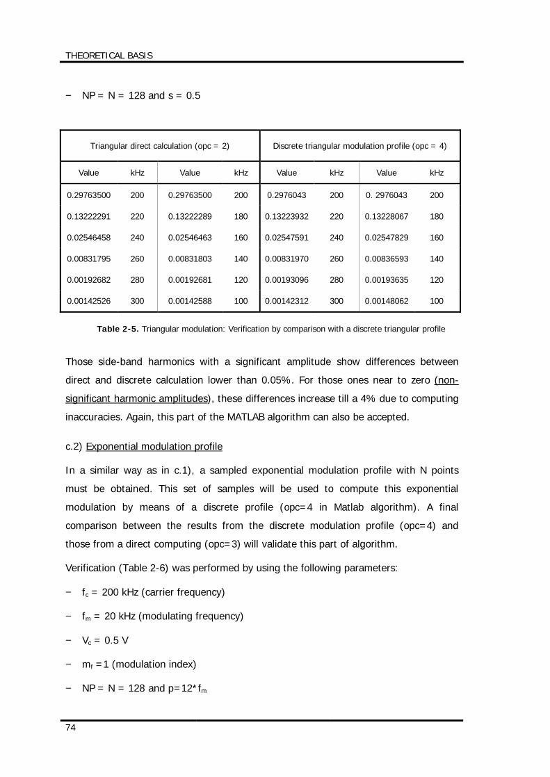
THEORETICAL BASIS
74
− NP = N = 128 and s = 0.5
Triangular direct calculation (opc = 2) Discrete triangular modulation profile (opc = 4)
Value kHz Value kHz Value kHz Value kHz
0.29763500 200 0.29763500 200 0.2976043 200 0. 2976043 200
0.13222291 220 0.13222289 180 0.13223932 220 0.13228067 180
0.02546458 240 0.02546463 160 0.02547591 240 0.02547829 160
0.00831795 260 0.00831803 140 0.00831970 260 0.00836593 140
0.00192682 280 0.00192681 120 0.00193096 280 0.00193635 120
0.00142526 300 0.00142588 100 0.00142312 300 0.00148062 100
Table 2-5. Triangular modulation: Verification by comparison with a discrete triangular profile
Those side-band harmonics with a significant amplitude show differences between
direct and discrete calculation lower than 0.05%. For those ones near to zero (non-
significant harmonic amplitudes), these differences increase till a 4% due to computing
inaccuracies. Again, this part of the MATLAB algorithm can also be accepted.
c.2) Exponential modulation profile
In a similar way as in c.1), a sampled exponential modulation profile with N points
must be obtained. This set of samples will be used to compute this exponential
modulation by means of a discrete profile (opc=4 in Matlab algorithm). A final
comparison between the results from the discrete modulation profile (opc=4) and
those from a direct computing (opc=3) will validate this part of algorithm.
Verification (Table 2-6) was performed by using the following parameters:
− fc = 200 kHz (carrier frequency)
− fm = 20 kHz (modulating frequency)
− Vc = 0.5 V
− mf =1 (modulation index)
− NP = N = 128 and p=12*fm
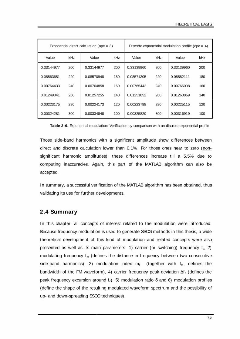
THEORETICAL BASIS
75
Exponential direct calculation (opc = 3) Discrete exponential modulation profile (opc = 4)
Value kHz Value kHz Value kHz Value kHz
0.33144977 200 0.33144977 200 0.33139960 200 0.33139960 200
0.08563651 220 0.08570948 180 0.08571305 220 0.08582111 180
0.00764433 240 0.00764858 160 0.00765442 240 0.00766008 160
0.01249041 260 0.01257255 140 0.01251852 260 0.01263869 140
0.00223175 280 0.00224173 120 0.00223788 280 0.00225115 120
0.00324281 300 0.00334848 100 0.00325820 300 0.00316919 100
Table 2-6. Exponential modulation: Verification by comparison with an discrete exponential profile
Those side-band harmonics with a significant amplitude show differences between
direct and discrete calculation lower than 0.1%. For those ones near to zero (non-
significant harmonic amplitudes), these differences increase till a 5.5% due to
computing inaccuracies. Again, this part of the MATLAB algorithm can also be
accepted.
In summary, a successful verification of the MATLAB algorithm has been obtained, thus
validating its use for further developments.
2.4 Summary
In this chapter, all concepts of interest related to the modulation were introduced.
Because frequency modulation is used to generate SSCG methods in this thesis, a wide
theoretical development of this kind of modulation and related concepts were also
presented as well as its main parameters: 1) carrier (or switching) frequency fc, 2)
modulating frequency fm (defines the distance in frequency between two consecutive
side-band harmonics), 3) modulation index mf (together with fm, defines the
bandwidth of the FM waveform), 4) carrier frequency peak deviation ∆fc (defines the
peak frequency excursion around fc), 5) modulation ratio δ and 6) modulation profiles
(define the shape of the resulting modulated waveform spectrum and the possibility of
up- and down-spreading SSCG techniques).
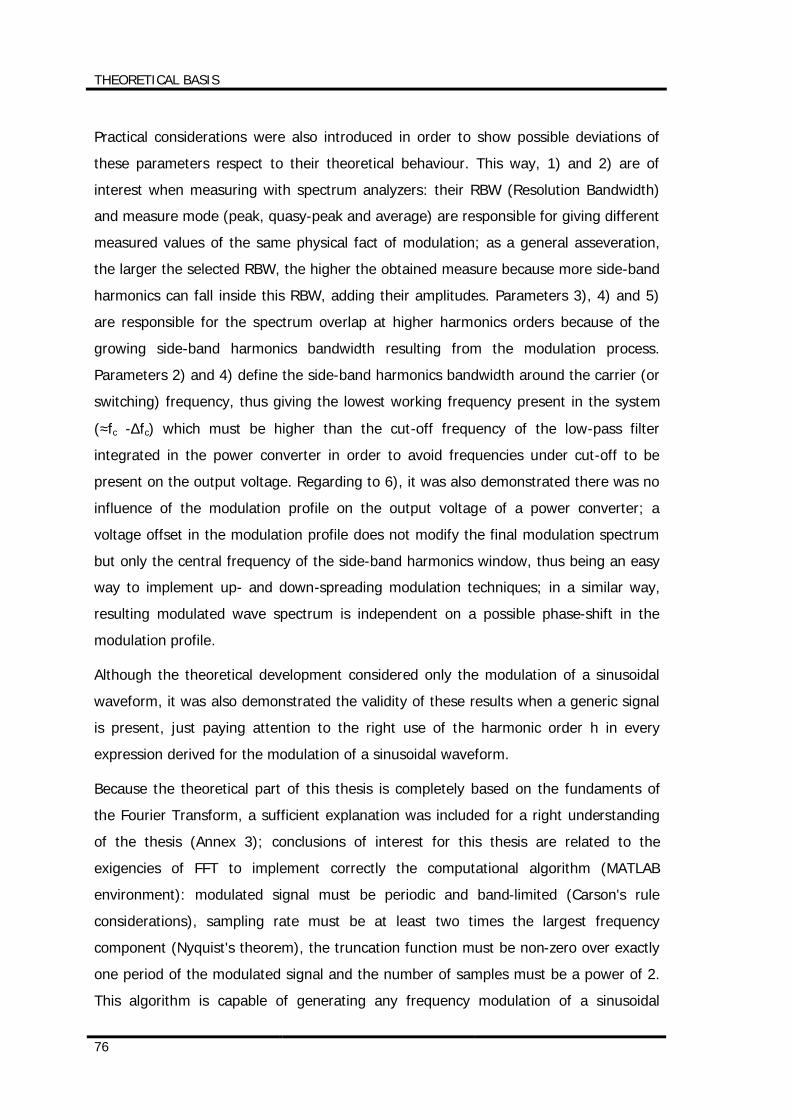
THEORETICAL BASIS
76
Practical considerations were also introduced in order to show possible deviations of
these parameters respect to their theoretical behaviour. This way, 1) and 2) are of
interest when measuring with spectrum analyzers: their RBW (Resolution Bandwidth)
and measure mode (peak, quasy-peak and average) are responsible for giving different
measured values of the same physical fact of modulation; as a general asseveration,
the larger the selected RBW, the higher the obtained measure because more side-band
harmonics can fall inside this RBW, adding their amplitudes. Parameters 3), 4) and 5)
are responsible for the spectrum overlap at higher harmonics orders because of the
growing side-band harmonics bandwidth resulting from the modulation process.
Parameters 2) and 4) define the side-band harmonics bandwidth around the carrier (or
switching) frequency, thus giving the lowest working frequency present in the system
(≈fc -∆fc) which must be higher than the cut-off frequency of the low-pass filter
integrated in the power converter in order to avoid frequencies under cut-off to be
present on the output voltage. Regarding to 6), it was also demonstrated there was no
influence of the modulation profile on the output voltage of a power converter; a
voltage offset in the modulation profile does not modify the final modulation spectrum
but only the central frequency of the side-band harmonics window, thus being an easy
way to implement up- and down-spreading modulation techniques; in a similar way,
resulting modulated wave spectrum is independent on a possible phase-shift in the
modulation profile.
Although the theoretical development considered only the modulation of a sinusoidal
waveform, it was also demonstrated the validity of these results when a generic signal
is present, just paying attention to the right use of the harmonic order h in every
expression derived for the modulation of a sinusoidal waveform.
Because the theoretical part of this thesis is completely based on the fundaments of
the Fourier Transform, a sufficient explanation was included for a right understanding
of the thesis (Annex 3); conclusions of interest for this thesis are related to the
exigencies of FFT to implement correctly the computational algorithm (MATLAB
environment): modulated signal must be periodic and band-limited (Carson's rule
considerations), sampling rate must be at least two times the largest frequency
component (Nyquist's theorem), the truncation function must be non-zero over exactly
one period of the modulated signal and the number of samples must be a power of 2.
This algorithm is capable of generating any frequency modulation of a sinusoidal

THEORETICAL BASIS
77
carrier and the corresponding spectral components resulting from the modulation
process; three special modulation profiles were studied: sinusoidal, triangular and
exponential waveforms. A specific development was also carried out for a generic
discrete modulation profile. A verification procedure for the algorithm was also
presented in order to validate one of the most important parts of the thesis.

C H A P T E R
3
THEORETICAL ANALYSIS OF EMI WITH DIFFERENT
MODULATION PARAMETERS


THEORETICAL ANALYSIS OF EMI WITH DIFFERENT MODULATION PARAMETERS
81
3. THEORETICAL ANALYSIS OF EMI WITH
DIFFERENT MODULATION PARAMETERS
Chapter 3 takes profit of the results obtained in Chapter 2 and assumes them in order
to completely understand and analyze the theoretical behaviour of the modulation
profiles, providing simultaneously a quantification of the modulation process according
to several significant measure parameters. In order to systematize the theoretical
analysis of EMI, the following points are considered:
1. Evolution of significant parameters shown in Figures 3-1 and 3-2 is to be studied as
a function of the modulation index mf. A further demonstration will show that side-
band harmonic amplitudes resulting from the modulation process (and, therefore,
the shape or outline of the side-band harmonics window) only depends on the
modulation index mf.
This study must be accomplished for a significant range of modulation indexes. The
idea is to obtain a graphical behaviour of the attenuation for the specified range of
modulation indexes.
2. After the theoretical analysis in point 1 for the three modulation profiles of interest
(sinusoidal, triangular and exponential waveforms), a comparison of these profiles
is to be carried out according to the measure parameters defined in Figure 3-2.
3. It is also presented a theoretical proposal of control for a switching power
converter and derived some considerations to apply a certain SSCG method in
power converters in order to reduce EMI emissions.
The two first previous points are to be developed for every modulation profile under
study, that is, sinusoidal, triangular, exponential and mixed profiles.
Figure 3-1 shows the main parameters describing the harmonic spectrum resulting
from the modulation process at which a sinusoidal carrier has been subjected. A
definition of these parameters is done onwards:
− fc is the carrier frequency. When no modulation is present, a single harmonic (dot
line) appears in the whole spectra.
THEORETICAL ANALYSIS OF EMI WITH DIFFERENT MODULATION PARAMETERS
82
− F (or Vrms,carrier) is the RMS-amplitude (in volts) of the harmonic corresponding to
the non-modulated carrier waveform at a frequency fc. This value is fixed at
25.0 =0.354 volts.
− F1 is the RMS-amplitude (in volts) of the harmonic corresponding to the modulated
waveform at a frequency fc.
− Fenv,peak is the maximum RMS-amplitude (in volts) of the side-band harmonic
envelope corresponding to the modulated waveform.
− B is the side-band harmonic window bandwidth resulting from the modulation
process. It can be estimated by using the Carson's rule (see considerations in
clause 2.1.2).
− ∆fpeak is the distance in frequency between the two envelope peaks of value
Fenv,peak.
Figure 3-1. Definition of parameters to use in further analysis
However, theoretical results are to be presented as relative values respect to the non-
modulated harmonic amplitude (carrier) and expressed in dB (the commonest units in
EMC/EMI). Conversion of previous values to accomplish this exigency is done as
follows:
FV
VV
V parameterrms
carrierrms
parameterrmsrel
,
,
, == è (3-1)
F
Fenv,peak
fc
B
∆fpeak
Non-modulated harmonic
Side-band harmonic window after modulation
F1
f
vRMS
0 V

THEORETICAL ANALYSIS OF EMI WITH DIFFERENT MODULATION PARAMETERS
83
( ) ( ) ( )carrierrmsparameterrmsrel VVV ,10,1010 log20log20log20 ⋅−⋅=⋅ (3-2)
dBVrel = dBVparameter – (-9.0309 dBV) (3-3)
In other words, parameters presented in Figure 3-1 are finally displayed following the
schema exposed in Figure 3-2. All parameters and expressions regarding amplitudes
(mainly, F1 and Fenv,peak) are to be expressed along this chapter as relative values
respect to the non-modulated signal amplitude, that is, according to Figure 3-2.
Figure 3-2. Re-definition of parameters to be finally used in further graphical representations
Next points are dedicated to the theoretical study of sinusoidal, triangular and
exponential modulation profile.
3.1 Sinusoidal modulation profile
This is a very accurate starting point because analytical expressions are available for
this modulation profile, thus conclusions from experimental results by means of a right
theoretical interpretation can be derived. Afterwards, this procedure will be applied to
the rest of modulation profiles, of which no analytical expressions have been
developed.
Fenv,peak
fc
B
∆fpeak Non-modulated harmonic
Side-band harmonics window after modulation
f
dBVrel
dBVref
0 dBV
F1
THEORETICAL ANALYSIS OF EMI WITH DIFFERENT MODULATION PARAMETERS
84
Just to remember, in point 2.3.5, the analytical expression of a sinusoidal carrier
modulated by a sinusoidal modulation profile was derived:
tmJVtF cfc ωcos)()( 0=
( ) ( )[ ]ttmJ mcmcf ⋅−−⋅+⋅+ ωωωω coscos)(1
( ) ( )[ ]ttmJ mcmcf ⋅−+⋅+⋅+ ωωωω 2cos2cos)(2
( ) ( )[ ]ttmJ mcmcf ⋅−−⋅+⋅+ ωωωω 3cos3cos)(3
( ) ( )[ ]ttmJ mcmcf ⋅−+⋅+⋅+ ωωωω 4cos4cos)(4
...+ (3-4)
In other words, amplitudes of side-band harmonics depend only on the modulation
index as the argument of the Bessel functions.
This is the main reason for the graphical results in the next sections to be presented as
a function of the modulation index, mainly applying to all parameters in Figure 3-2
related to amplitude values. Because the modulation index mf is a ratio between the
product of the modulation ratio δ and the carrier frequency fc and the modulating
frequency fm (m
cf f
fm ⋅=
δ), it can be derived that different combinations of these three
parameters are to produce the same amplitude results of the side-band harmonics
resulting from the modulation process. This way, the modulation index becomes a very
helpful figure of merit because it summarizes the complete behaviour of three different
parameters (δ, fc and fm) working together in just one variable, that is, the modulation
index.
Although the side-band harmonics amplitudes are only depending on the modulation
index for a sinusoidal modulation, this behaviour must be firstly verified for the rest of
modulation profiles in order to apply the same analysis which is to be carried out for
the sinusoidal modulation profile, making the comparison between different modulation
profiles easier to display and the related conclusions to derive, one of the main
objectives of this thesis.
As shown in the following pictures (Figures 3-3 and 3-4), Bessel functions decrease in
amplitude at higher values of modulation index mf.

THEORETICAL ANALYSIS OF EMI WITH DIFFERENT MODULATION PARAMETERS
85
Figure 3-3. Bessel functions of several orders (up to mf = 50)
(NOTE: Expression in Figures 3-3 and 3-4 related to Bessel functions must be
understood this way è )(),( mJmkJ kn ≡ )
Figure 3-4 shows the amplitude evolution of Bessel functions for a larger value of
modulation index (mf = 1000). Up to mf ≈ 200, peak amplitude is decreasing
considerably for Bessel functions of any order.
Figure 3-4. Bessel functions of several orders (up to mf = 1000)
From the Bessel functions plot above, it must be concluded that amplitudes of the side-
band harmonics are to decrease as the modulation index mf gets higher. Anyway, from
mf ≈ 200 onwards, only slightly differences in amplitude should be expected. This is an
important point to be observed in the following analysis.
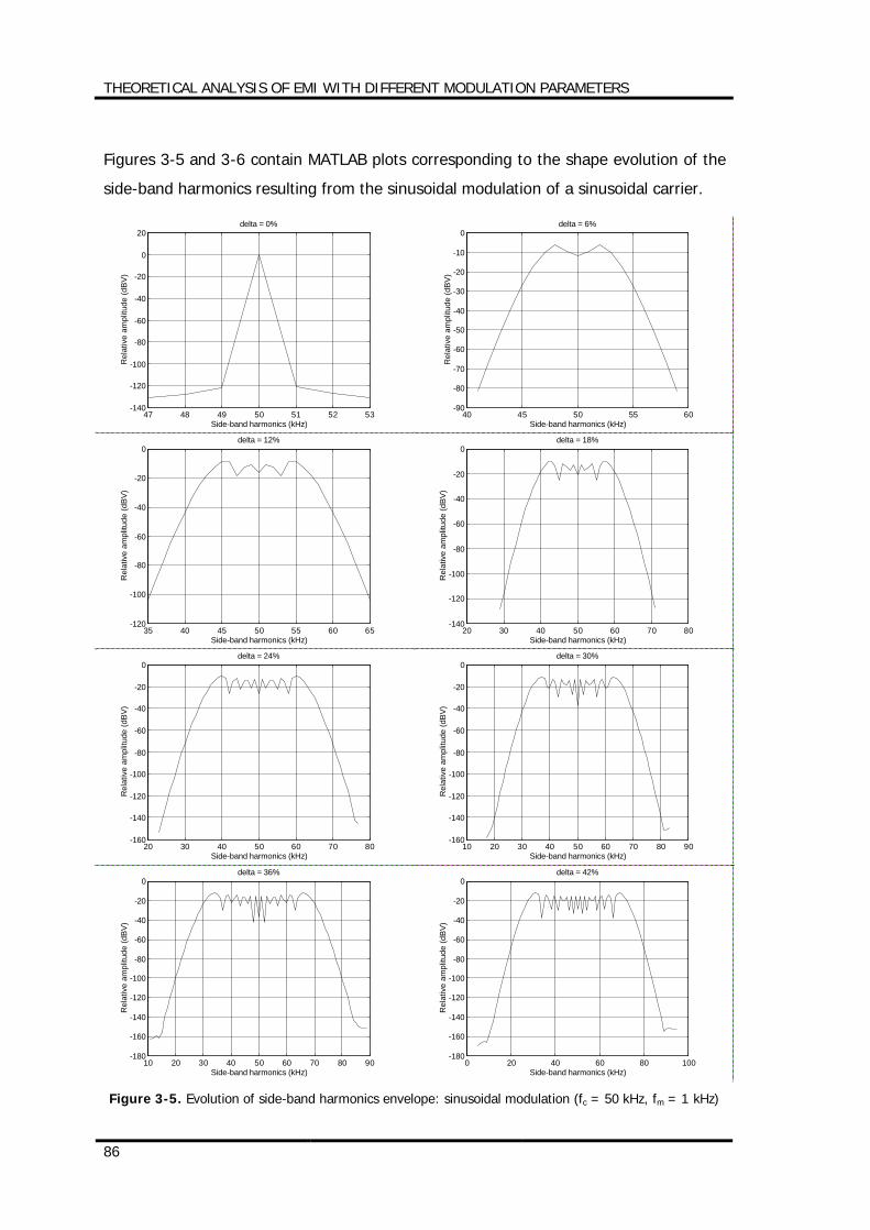
THEORETICAL ANALYSIS OF EMI WITH DIFFERENT MODULATION PARAMETERS
86
Figures 3-5 and 3-6 contain MATLAB plots corresponding to the shape evolution of the
side-band harmonics resulting from the sinusoidal modulation of a sinusoidal carrier.
47 48 49 50 51 52 53-140
-120
-100
-80
-60
-40
-20
0
20delta = 0%
Side-band harmonics (kHz)
Rel
ativ
e am
plitu
de (d
BV)
40 45 50 55 60
-90
-80
-70
-60
-50
-40
-30
-20
-10
0delta = 6%
Side-band harmonics (kHz)
Rel
ativ
e am
plitu
de (d
BV)
35 40 45 50 55 60 65-120
-100
-80
-60
-40
-20
0delta = 12%
Side-band harmonics (kHz)
Rel
ativ
e am
plitu
de (d
BV)
20 30 40 50 60 70 80
-140
-120
-100
-80
-60
-40
-20
0delta = 18%
Side-band harmonics (kHz)
Rel
ativ
e am
plitu
de (d
BV)
20 30 40 50 60 70 80-160
-140
-120
-100
-80
-60
-40
-20
0delta = 24%
Side-band harmonics (kHz)
Rel
ativ
e am
plitu
de (d
BV)
10 20 30 40 50 60 70 80 90
-160
-140
-120
-100
-80
-60
-40
-20
0delta = 30%
Side-band harmonics (kHz)
Rel
ativ
e am
plitu
de (d
BV)
10 20 30 40 50 60 70 80 90-180
-160
-140
-120
-100
-80
-60
-40
-20
0delta = 36%
Side-band harmonics (kHz)
Rel
ativ
e am
plitu
de (d
BV)
0 20 40 60 80 100
-180
-160
-140
-120
-100
-80
-60
-40
-20
0delta = 42%
Side-band harmonics (kHz)
Rel
ativ
e am
plitu
de (d
BV)
Figure 3-5. Evolution of side-band harmonics envelope: sinusoidal modulation (fc = 50 kHz, fm = 1 kHz)
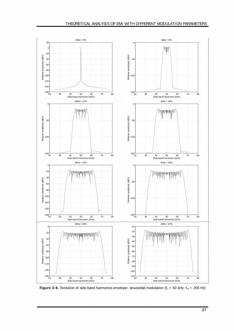
THEORETICAL ANALYSIS OF EMI WITH DIFFERENT MODULATION PARAMETERS
87
20 30 40 50 60 70 80-160
-140
-120
-100
-80
-60
-40
-20
0
20
Side-band harmonics (kHz)
Rel
ativ
e am
plitu
de (d
BV)
delta = 0%
20 30 40 50 60 70 80
-150
-100
-50
0delta = 6%
Side-band harmonics (kHz)
Rel
ativ
e am
plitu
de (d
BV)
20 30 40 50 60 70 80-150
-100
-50
0
Side-band harmonics (kHz)
Rel
ativ
e am
plitu
de (d
BV)
delta = 12%
20 30 40 50 60 70 80
-150
-100
-50
0delta = 18%
Side-band harmonics (kHz)
Rel
ativ
e am
plitu
de (d
BV)
20 30 40 50 60 70 80-160
-140
-120
-100
-80
-60
-40
-20
0
Side-band harmonics (kHz)
Rel
ativ
e am
plitu
de (d
BV)
delta = 24%
20 30 40 50 60 70 80
-150
-100
-50
0delta = 30%
Side-band harmonics (kHz)
Rel
ativ
e am
plitu
de (d
BV)
20 30 40 50 60 70 80-160
-140
-120
-100
-80
-60
-40
-20
0
Side-band harmonics (kHz)
Rel
ativ
e am
plitu
de (d
BV)
delta = 36%
20 30 40 50 60 70 80
-110
-100
-90
-80
-70
-60
-50
-40
-30
-20
-10delta = 42%
Side-band harmonics (kHz)
Rel
ativ
e am
plitu
de (d
BV)
Figure 3-6. Evolution of side-band harmonics envelope: sinusoidal modulation (fc = 50 kHz, fm = 200 Hz)
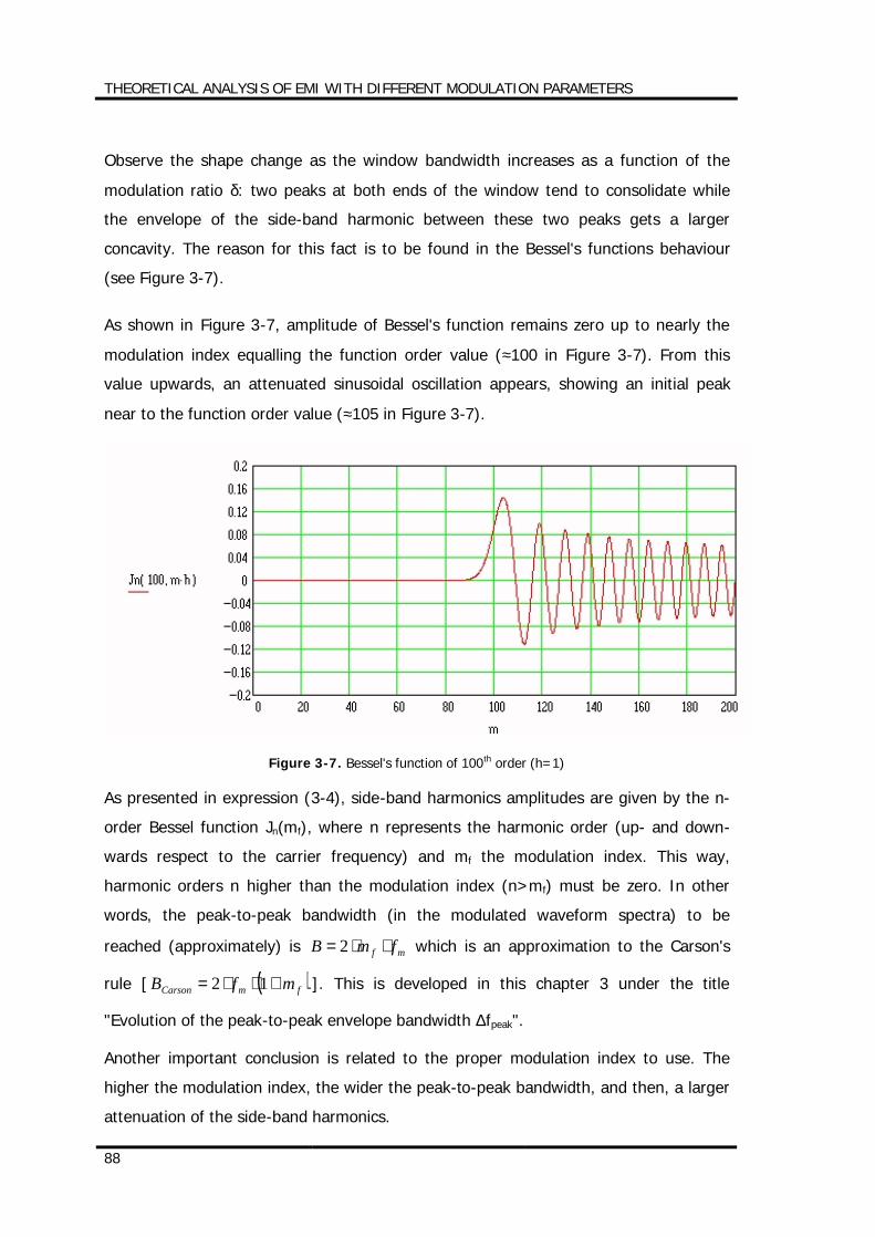
THEORETICAL ANALYSIS OF EMI WITH DIFFERENT MODULATION PARAMETERS
88
Observe the shape change as the window bandwidth increases as a function of the
modulation ratio δ: two peaks at both ends of the window tend to consolidate while
the envelope of the side-band harmonic between these two peaks gets a larger
concavity. The reason for this fact is to be found in the Bessel's functions behaviour
(see Figure 3-7).
As shown in Figure 3-7, amplitude of Bessel's function remains zero up to nearly the
modulation index equalling the function order value (≈100 in Figure 3-7). From this
value upwards, an attenuated sinusoidal oscillation appears, showing an initial peak
near to the function order value (≈105 in Figure 3-7).
Figure 3-7. Bessel's function of 100th order (h=1)
As presented in expression (3-4), side-band harmonics amplitudes are given by the n-
order Bessel function Jn(mf), where n represents the harmonic order (up- and down-
wards respect to the carrier frequency) and mf the modulation index. This way,
harmonic orders n higher than the modulation index (n>mf) must be zero. In other
words, the peak-to-peak bandwidth (in the modulated waveform spectra) to be
reached (approximately) is mf fmB ⋅⋅= 2 which is an approximation to the Carson's
rule [ ( )fmCarson mfB +⋅⋅= 12 ]. This is developed in this chapter 3 under the title
"Evolution of the peak-to-peak envelope bandwidth ∆fpeak".
Another important conclusion is related to the proper modulation index to use. The
higher the modulation index, the wider the peak-to-peak bandwidth, and then, a larger
attenuation of the side-band harmonics.
THEORETICAL ANALYSIS OF EMI WITH DIFFERENT MODULATION PARAMETERS
89
3.1.1 Evolution of the central harmonic amplitude F1
In the following Figures 3-8(a) and 3-8(b), F1 (relative amplitude of the harmonic
corresponding to the modulated waveform at a frequency fc) is displayed (blue line) as
a function of the modulation index mf. Figure 3-8(a) consists of four graphs, each one
at a different range of modulation indexes, till mf = 500; Figure 3-8(b) shows the same
values till a modulation index mf = 2000. This way, a wide range of modulation indexes
is covered for a complete variety of parameters values, as shown in Table 3-1.
fc (kHz) Carrier frequency
fm (kHz) Modulating frequency
δ% (%) Percentage of modulation m
cf f
fm ⋅=
δ
50 ÷1000 0.25 ÷20 0 ÷50 200025.010005.0
=⋅
Table 3-1.Values of the different parameters and maximum value expected for mf
Besides, the maximum amplitude of the harmonics envelope (Fenv,peak) is also included
in these figures (red line) in order to compare visually the different attenuation of
these two parameters.
In every case, an oscillation of the amplitude F1 is present; however, an envelope can
be defined, consisting of a logarithmic curve joining the local maximum points of every
individual oscillation. This logarithmic curve gives the maximum attenuation possible
with the selected parameters: δ%, fc and fm. However, a larger attenuation is also
possible, just selecting the proper point where the oscillation reaches a minimum
value. For instance, for mf > 4 (see Figure 3-8(a)), an attenuation larger than -8 dBV is
always to be obtained; however, for mf = 5.52, an attenuation larger than -90 dBV is
available. In other words, a special profit of this individual behaviour can be taken just
tuning the system to a concrete modulation index in order, for instance, to eliminate
the harmonic at the carrier frequency.
As the sinusoidal frequency modulation of a sinusoidal carrier was derived theoretically
and an analytical expression (3-4) was obtained, a specific profit of this fact is to be
taken in order to analyse and interpret the MATLAB-algorithm results (shown in Figures
3-8(a) and 3-8(b)) to justify them by comparing them to the theoretical ones.
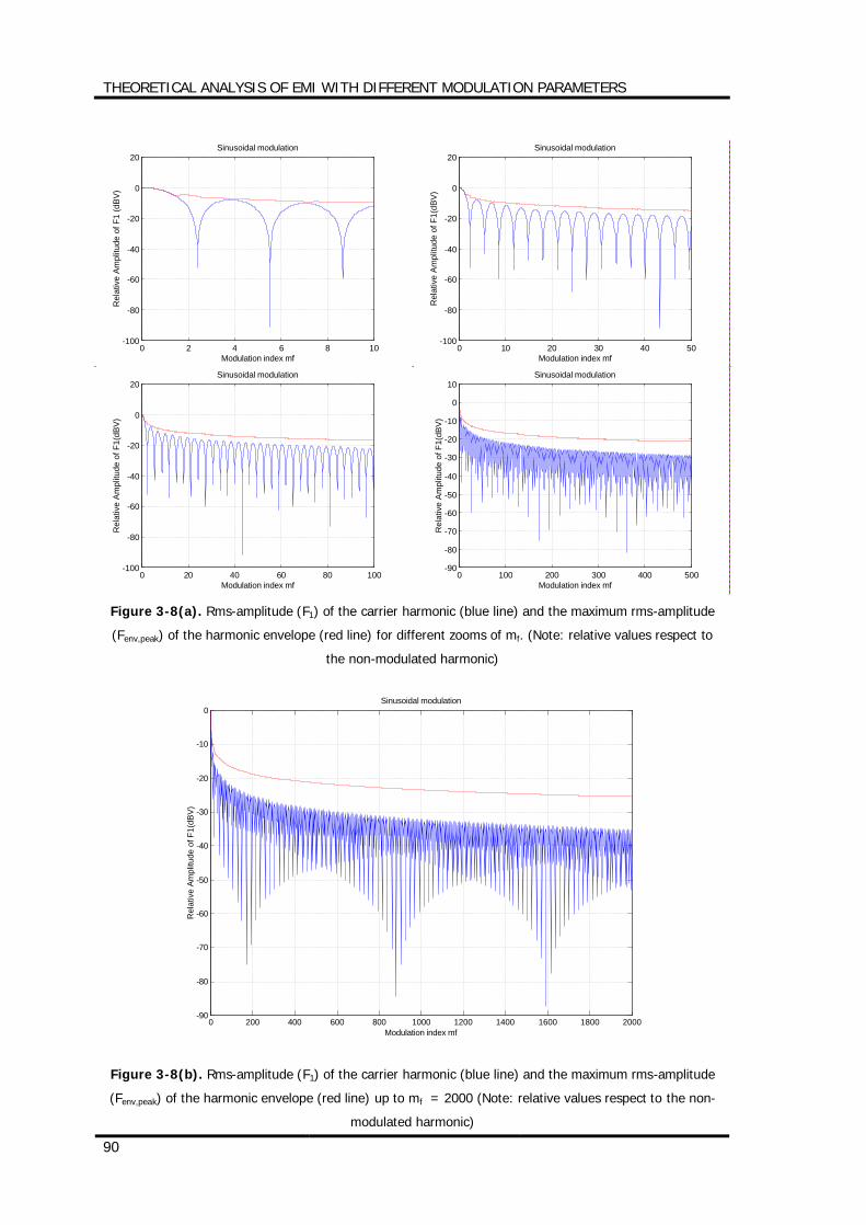
THEORETICAL ANALYSIS OF EMI WITH DIFFERENT MODULATION PARAMETERS
90
0 2 4 6 8 10-100
-80
-60
-40
-20
0
20
Modulation index mf
Rel
ativ
e Am
plitu
de o
f F1
(dBV
)
Sinusoidal modulation
0 10 20 30 40 50
-100
-80
-60
-40
-20
0
20
Modulation index mf
Rel
ativ
e Am
plitu
de o
f F1(
dBV)
Sinusoidal modulation
0 20 40 60 80 100-100
-80
-60
-40
-20
0
20
Modulation index mf
Rel
ativ
e Am
plitu
de o
f F1(
dBV)
Sinusoidal modulation
0 100 200 300 400 500
-90
-80
-70
-60
-50
-40
-30
-20
-10
0
10
Modulation index mf
Rel
ativ
e Am
plitu
de o
f F1(
dBV)
Sinusoidal modulation
Figure 3-8(a). Rms-amplitude (F1) of the carrier harmonic (blue line) and the maximum rms-amplitude
(Fenv,peak) of the harmonic envelope (red line) for different zooms of mf. (Note: relative values respect to
the non-modulated harmonic)
0 200 400 600 800 1000 1200 1400 1600 1800 2000-90
-80
-70
-60
-50
-40
-30
-20
-10
0
Modulation index mf
Rel
ativ
e Am
plitu
de o
f F1(
dBV)
Sinusoidal modulation
Figure 3-8(b). Rms-amplitude (F1) of the carrier harmonic (blue line) and the maximum rms-amplitude
(Fenv,peak) of the harmonic envelope (red line) up to mf = 2000 (Note: relative values respect to the non-
modulated harmonic)
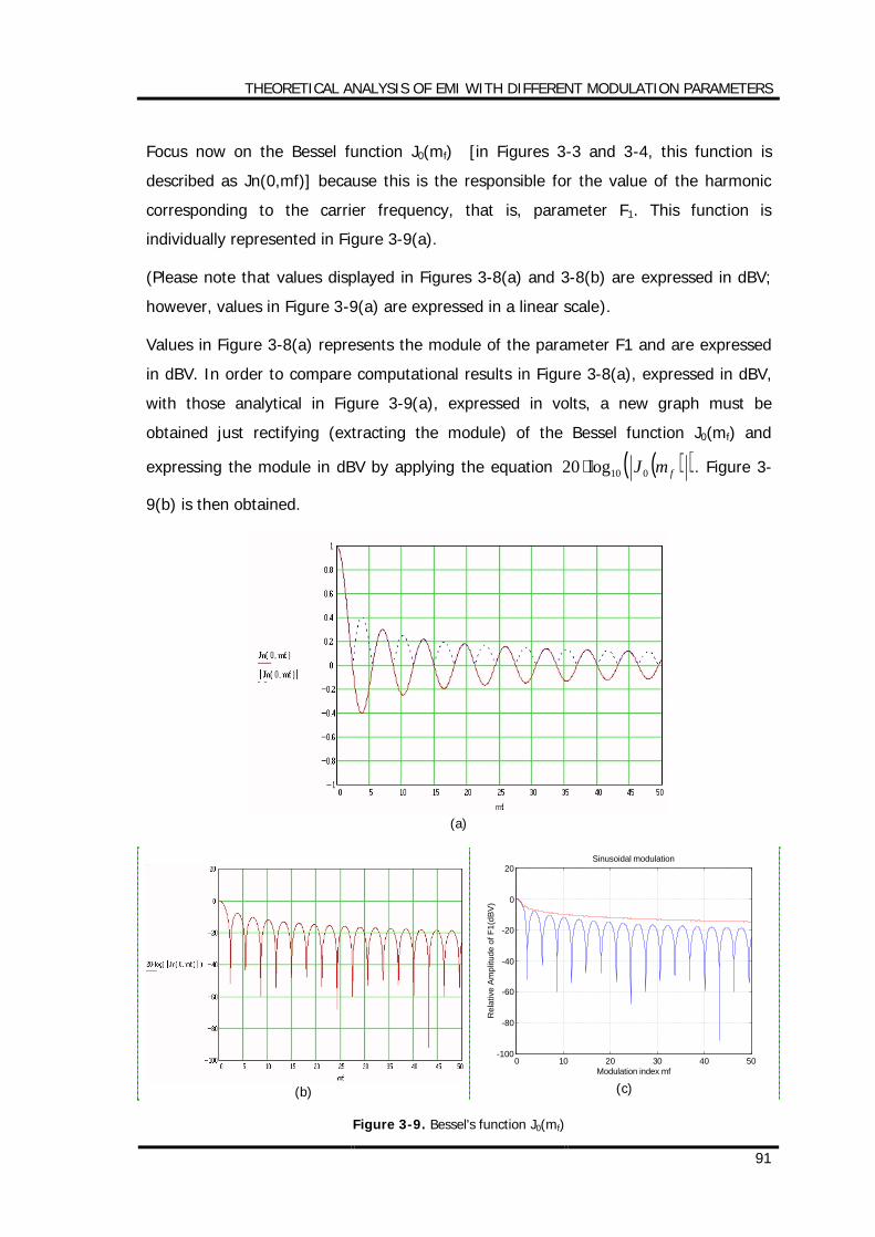
THEORETICAL ANALYSIS OF EMI WITH DIFFERENT MODULATION PARAMETERS
91
Focus now on the Bessel function J0(mf) [in Figures 3-3 and 3-4, this function is
described as Jn(0,mf)] because this is the responsible for the value of the harmonic
corresponding to the carrier frequency, that is, parameter F1. This function is
individually represented in Figure 3-9(a).
(Please note that values displayed in Figures 3-8(a) and 3-8(b) are expressed in dBV;
however, values in Figure 3-9(a) are expressed in a linear scale).
Values in Figure 3-8(a) represents the module of the parameter F1 and are expressed
in dBV. In order to compare computational results in Figure 3-8(a), expressed in dBV,
with those analytical in Figure 3-9(a), expressed in volts, a new graph must be
obtained just rectifying (extracting the module) of the Bessel function J0(mf) and
expressing the module in dBV by applying the equation ( )( )fmJ010log20 ⋅ . Figure 3-
9(b) is then obtained.
(a)
(b)
0 10 20 30 40 50-100
-80
-60
-40
-20
0
20
Modulation index mf
Rel
ativ
e Am
plitu
de o
f F1(
dBV)
Sinusoidal modulation
(c)
Figure 3-9. Bessel's function J0(mf)
THEORETICAL ANALYSIS OF EMI WITH DIFFERENT MODULATION PARAMETERS
92
Figure 3-8(a) is presented again in Figure 3-9(c) for convenience. It is easy to see that
the shape of the F1 parameter in Figure 3-9(c) [range mf =0 to 50] matches exactly
the one in Figure 3-9(b).
Other important conclusions are listed below:
− As expected from expression (3-4), higher modulation indexes mf are to produce
higher attenuation (regarding the envelope of F1). For instance, for mf = 4,
attenuation of F1 –envelope is -8 dBV while for mf = 20, attenuation is -15 dBV.
− Difference between the F1 -envelope and the parameter Fenv,peak increases with the
modulation index mf, that is, the larger mf, the larger the difference between F1 -
envelope and Fenv,peak, and, thus, the larger concavity of the side-band spectra
envelope.
− Because of the logarithmic behaviour, it is observed that attenuation remains
approximately constant for modulation indexes higher than ≈200; in other words, it
is not worthy to design modulation processes with higher modulation indexes.
Therefore, higher modulation indexes should be selected and, through its
definitionm
cf f
fm ⋅=
δ, this can be done by increasing the modulation ratio δ or the
carrier frequency fc or decreasing the modulating frequency fm.
3.1.2 Evolution of the maximum envelope amplitude Fenv,peak
Another important parameter to be analysed corresponds to the maximum rms-
amplitude of the side-band harmonic envelope corresponding to the modulated
waveform, Fenv,peak. The Matlab algorithm presented in clause 2.3 calculates these
values just storing the maximum value at each modulation index or iteration. Figures
3-10(a) and 3-10(b) show the behaviour of this parameter versus the modulation
index. Figure 3-10(a) consists of four graphs, each one at a different range of
modulation indexes, till mf = 500; Figure 3-10(b) shows the same values till a
modulation index mf = 2000. This way, the complete range of modulation indexes is
covered for the complete variety of parameters values (see Table 3-1).
In every case, an oscillation of the amplitudes Fenv,peak is present; however, a
logarithmic envelope defined by joining the local maximum points of every individual
oscillation is found.
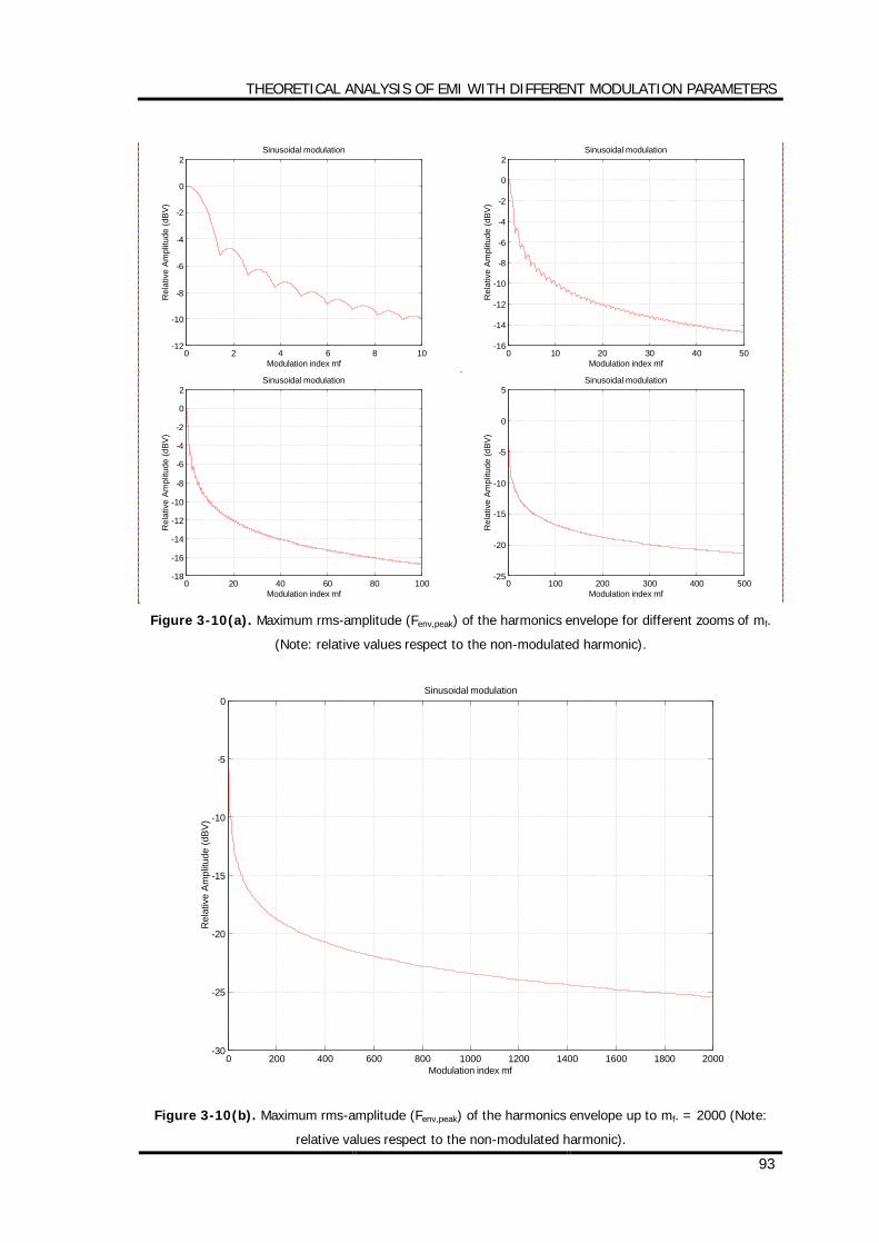
THEORETICAL ANALYSIS OF EMI WITH DIFFERENT MODULATION PARAMETERS
93
0 2 4 6 8 10-12
-10
-8
-6
-4
-2
0
2
Modulation index mf
Rel
ativ
e Am
plitu
de (d
BV)
Sinusoidal modulation
0 10 20 30 40 50
-16
-14
-12
-10
-8
-6
-4
-2
0
2
Modulation index mf
Rel
ativ
e Am
plitu
de (d
BV)
Sinusoidal modulation
0 20 40 60 80 100-18
-16
-14
-12
-10
-8
-6
-4
-2
0
2
Modulation index mf
Rel
ativ
e Am
plitu
de (d
BV)
Sinusoidal modulation
0 100 200 300 400 500
-25
-20
-15
-10
-5
0
5
Modulation index mf
Rel
ativ
e Am
plitu
de (d
BV)
Sinusoidal modulation
Figure 3-10(a). Maximum rms-amplitude (Fenv,peak) of the harmonics envelope for different zooms of mf.
(Note: relative values respect to the non-modulated harmonic).
0 200 400 600 800 1000 1200 1400 1600 1800 2000-30
-25
-20
-15
-10
-5
0
Modulation index mf
Rel
ativ
e Am
plitu
de (d
BV)
Sinusoidal modulation
Figure 3-10(b). Maximum rms-amplitude (Fenv,peak) of the harmonics envelope up to mf. = 2000 (Note:
relative values respect to the non-modulated harmonic).
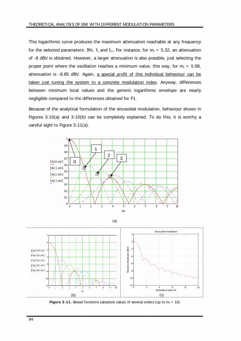
THEORETICAL ANALYSIS OF EMI WITH DIFFERENT MODULATION PARAMETERS
94
This logarithmic curve produces the maximum attenuation reachable at any frequency
for the selected parameters: δ%, fc and fm. For instance, for mf = 5.32, an attenuation
of -8 dBV is obtained. However, a larger attenuation is also possible, just selecting the
proper point where the oscillation reaches a minimum value; this way, for mf = 5.98,
attenuation is -8.85 dBV. Again, a special profit of this individual behaviour can be
taken just tuning the system to a concrete modulation index. Anyway, differences
between minimum local values and the generic logarithmic envelope are nearly
negligible compared to the differences obtained for F1.
Because of the analytical formulation of the sinusoidal modulation, behaviour shown in
Figures 3-10(a) and 3-10(b) can be completely explained. To do this, it is worthy a
careful sight to Figure 3-11(a).
(a)
(b)
0 2 4 6 8 10-12
-10
-8
-6
-4
-2
0
2
Modulation index mf
Rel
ativ
e Am
plitu
de (d
BV)
Sinusoidal modulation
(c)
Figure 3-11. Bessel functions (absolute value) of several orders (up to mf = 10)
1 2
3 0
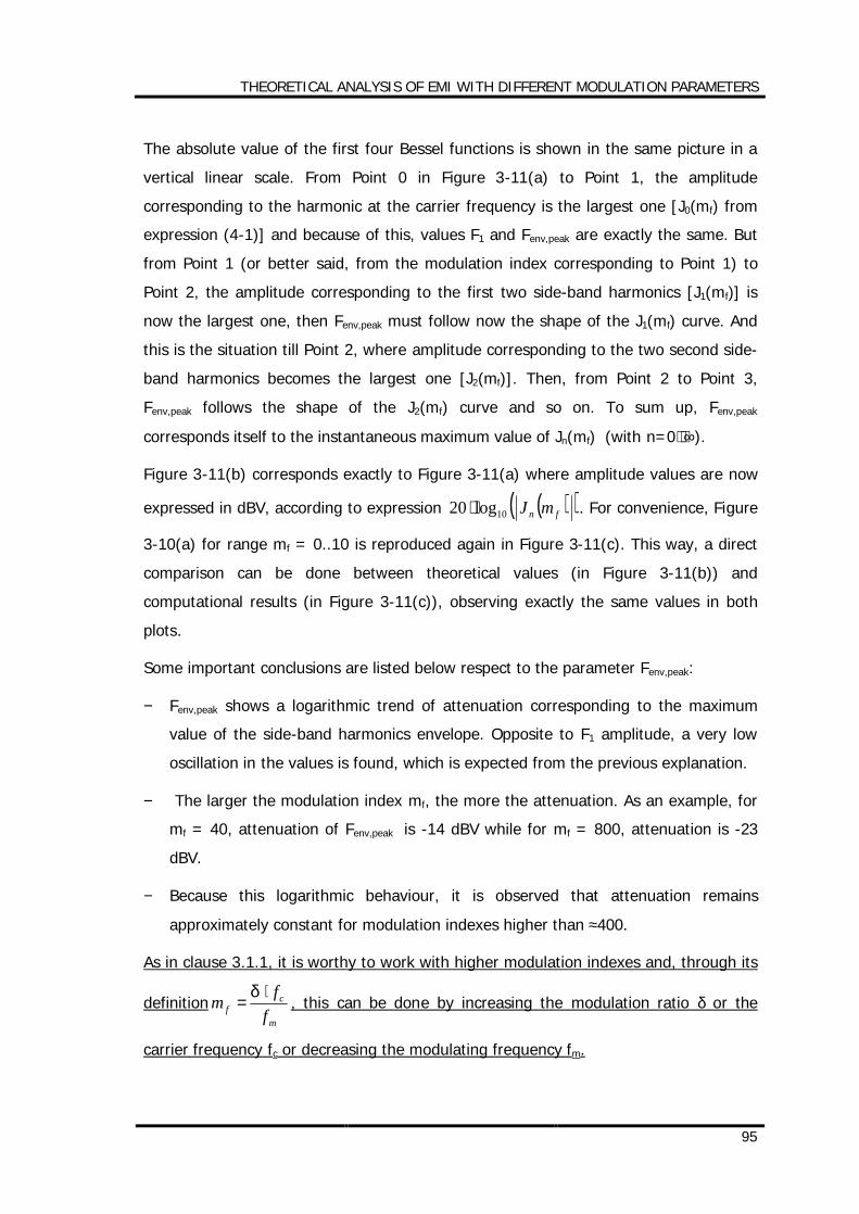
THEORETICAL ANALYSIS OF EMI WITH DIFFERENT MODULATION PARAMETERS
95
The absolute value of the first four Bessel functions is shown in the same picture in a
vertical linear scale. From Point 0 in Figure 3-11(a) to Point 1, the amplitude
corresponding to the harmonic at the carrier frequency is the largest one [J0(mf) from
expression (4-1)] and because of this, values F1 and Fenv,peak are exactly the same. But
from Point 1 (or better said, from the modulation index corresponding to Point 1) to
Point 2, the amplitude corresponding to the first two side-band harmonics [J1(mf)] is
now the largest one, then Fenv,peak must follow now the shape of the J1(mf) curve. And
this is the situation till Point 2, where amplitude corresponding to the two second side-
band harmonics becomes the largest one [J2(mf)]. Then, from Point 2 to Point 3,
Fenv,peak follows the shape of the J2(mf) curve and so on. To sum up, Fenv,peak
corresponds itself to the instantaneous maximum value of Jn(mf) (with n=0⋅⋅∞).
Figure 3-11(b) corresponds exactly to Figure 3-11(a) where amplitude values are now
expressed in dBV, according to expression ( )( )fn mJ10log20 ⋅ . For convenience, Figure
3-10(a) for range mf = 0..10 is reproduced again in Figure 3-11(c). This way, a direct
comparison can be done between theoretical values (in Figure 3-11(b)) and
computational results (in Figure 3-11(c)), observing exactly the same values in both
plots.
Some important conclusions are listed below respect to the parameter Fenv,peak:
− Fenv,peak shows a logarithmic trend of attenuation corresponding to the maximum
value of the side-band harmonics envelope. Opposite to F1 amplitude, a very low
oscillation in the values is found, which is expected from the previous explanation.
− The larger the modulation index mf, the more the attenuation. As an example, for
mf = 40, attenuation of Fenv,peak is -14 dBV while for mf = 800, attenuation is -23
dBV.
− Because this logarithmic behaviour, it is observed that attenuation remains
approximately constant for modulation indexes higher than ≈400.
As in clause 3.1.1, it is worthy to work with higher modulation indexes and, through its
definitionm
cf f
fm ⋅=
δ, this can be done by increasing the modulation ratio δ or the
carrier frequency fc or decreasing the modulating frequency fm.
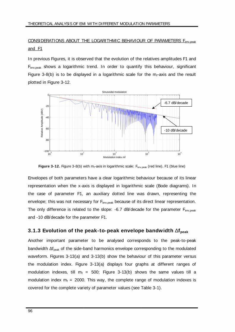
THEORETICAL ANALYSIS OF EMI WITH DIFFERENT MODULATION PARAMETERS
96
CONSIDERATIONS ABOUT THE LOGARITHMIC BEHAVIOUR OF PARAMETERS Fenv,peak
and F1
In previous Figures, it is observed that the evolution of the relatives amplitudes F1 and
Fenv,peak shows a logarithmic trend. In order to quantify this behaviour, significant
Figure 3-8(b) is to be displayed in a logarithmic scale for the mf-axis and the result
plotted in Figure 3-12.
100
101
102
103
104-100
-80
-60
-40
-20
0
Modulation index mf
Rel
ativ
e Am
plitu
de (d
BV)
Sinusoidal modulation
Figure 3-12. Figure 3-8(b) with mf-axis in logarithmic scale: Fenv,peak (red line), F1 (blue line)
Envelopes of both parameters have a clear logarithmic behaviour because of its linear
representation when the x-axis is displayed in logarithmic scale (Bode diagrams). In
the case of parameter F1, an auxiliary dotted line was drawn, representing the
envelope; this was not necessary for Fenv,peak because of its direct linear representation.
The only difference is related to the slope: -6.7 dB/decade for the parameter Fenv,peak
and -10 dB/decade for the parameter F1.
3.1.3 Evolution of the peak-to-peak envelope bandwidth ∆fpeak
Another important parameter to be analysed corresponds to the peak-to-peak
bandwidth ∆fpeak of the side-band harmonics envelope corresponding to the modulated
waveform. Figures 3-13(a) and 3-13(b) show the behaviour of this parameter versus
the modulation index. Figure 3-13(a) displays four graphs at different ranges of
modulation indexes, till mf = 500; Figure 3-13(b) shows the same values till a
modulation index mf = 2000. This way, the complete range of modulation indexes is
covered for the complete variety of parameter values (see Table 3-1).
-10 dB/decade
-6.7 dB/decade
THEORETICAL ANALYSIS OF EMI WITH DIFFERENT MODULATION PARAMETERS
97
A consecution of steps seems to be the behaviour of this parameter ∆fpeak vs. the
modulation index mf. Again and due to the analytical results obtained for a sinusoidal
modulation, this amusing behaviour can be derived. To do this, pay attention to Figure
3-11(a). Although infinity of side-band harmonics are always present in the modulated
waveform spectra, from Point 0 to Point 1, the harmonic corresponding to the carrier
frequency is the largest one, then yielding a null value for ∆fpeak. From Point 1 to Point
2, the amplitude corresponding to the first two side-band harmonics [J1(mf)] is now the
largest one; this means this range (Point 1-Point 2) is characterised for two harmonics
of largest amplitude, each one separated in frequency a quantity of fm from the carrier
frequency, that is, a total distance of 2⋅fm which corresponds to ∆fpeak. In the same
way, From Point 2 to Point 3, the amplitude corresponding to the second two side-
band harmonics [J2(mf)] becomes now the largest one which means that the range
Point 2-Point 3 is now characterised for two harmonics of largest amplitude, each one
separated in frequency a quantity of 2⋅fm from the carrier frequency, that is, a total
distance of 2⋅2⋅fm = 4⋅fm and so on. To sum up, From Point n to Point n+1, the
amplitude corresponding to the nth two side-band harmonics [Jn(mf)] becomes the
largest one which means that the range (Point n-Point n+1) is now characterised for
two harmonics of largest amplitude, each one separated in frequency a quantity of n⋅fm
from the carrier frequency, that is, a total distance of 2⋅n⋅fm. For instance, the first
picture in Figure 3-13(a) shows steps 20 kHz-high, due to the modulating frequency of
10 kHz.
Some important conclusions are listed below:
− Envelope of ∆fpeak shows a linear trend respect to mf, which confirms the related
analysis in point 3.1 where it was derived the expression mfpeak fmfB ⋅⋅≈∆= 2 . As
an example, in Figure 3-13(b), for a modulation index mf = 200 and a modulating
frequency fm = 250 Hz, ∆fpeak is equal to 97.5 kHz, value which can be estimated by
mfpeak fmfB ⋅⋅≈∆= 2 = 100 kHz.
− Higher modulation indexes mf are to produce wider bandwidths in a linear ratio.
− The step width remains practically constant through mf and equal to 2⋅fm.
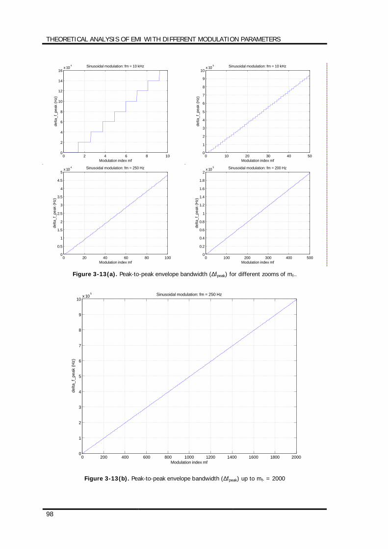
THEORETICAL ANALYSIS OF EMI WITH DIFFERENT MODULATION PARAMETERS
98
0 2 4 6 8 100
2
4
6
8
10
12
14
16x 10 4
Modulation index mf
delta
_f_p
eak
(Hz)
Sinusoidal modulation: fm = 10 kHz
0 10 20 30 40 50
0
1
2
3
4
5
6
7
8
9
10x 10 5
Modulation index mf
delta
_f_p
eak
(Hz)
Sinusoidal modulation: fm = 10 kHz
0 20 40 60 80 1000
0.5
1
1.5
2
2.5
3
3.5
4
4.5
5x 10 4
Modulation index mf
delta
_f_p
eak
(Hz)
Sinusoidal modulation: fm = 250 Hz
0 100 200 300 400 500
0
0.2
0.4
0.6
0.8
1
1.2
1.4
1.6
1.8
2x 10 5
Modulation index mf
delta
_f_p
eak
(Hz)
Sinusoidal modulation: fm = 200 Hz
Figure 3-13(a). Peak-to-peak envelope bandwidth (∆fpeak) for different zooms of mf..
0 200 400 600 800 1000 1200 1400 1600 1800 20000
1
2
3
4
5
6
7
8
9
10x 10
5
Modulation index mf
delta
_f_p
eak
(Hz)
Sinusoidal modulation: fm = 250 Hz
Figure 3-13(b). Peak-to-peak envelope bandwidth (∆fpeak) up to mf. = 2000
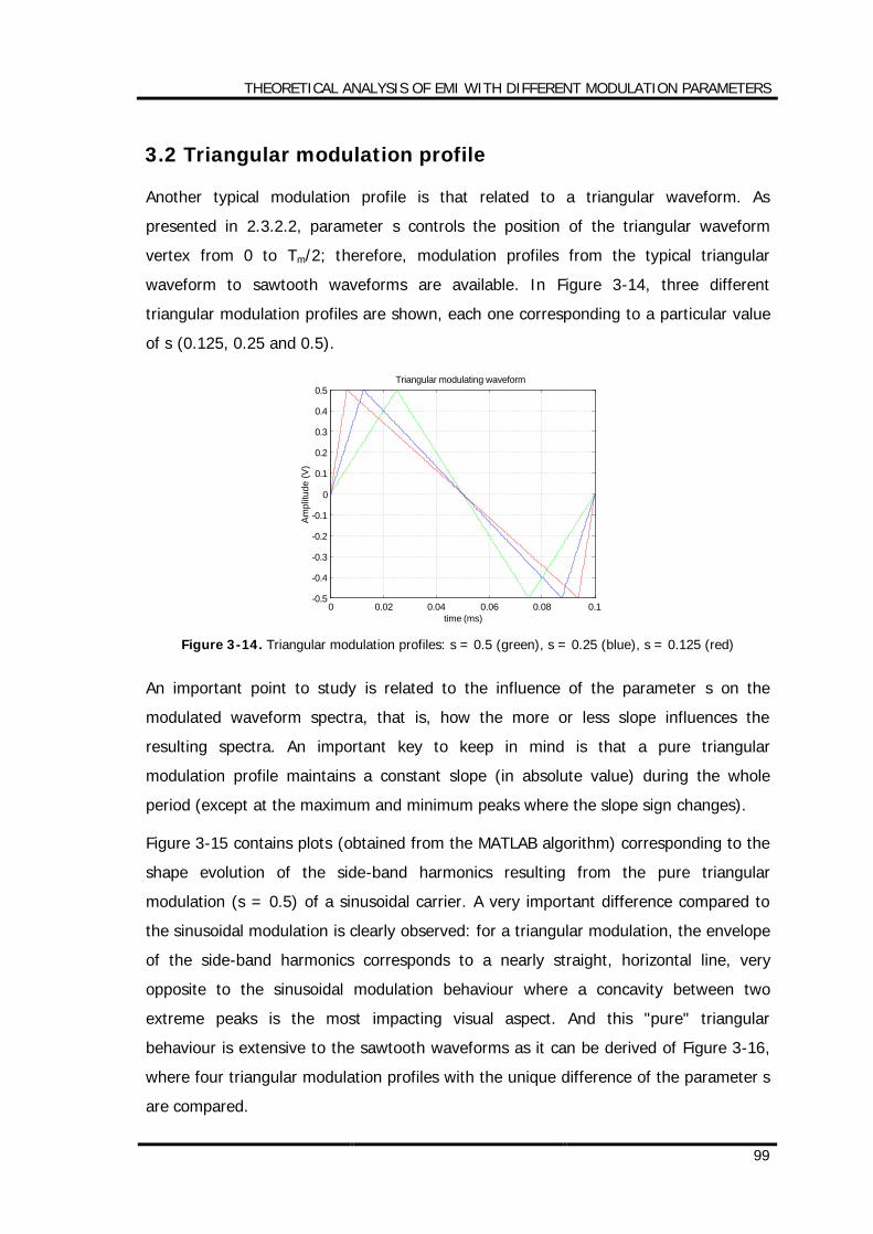
THEORETICAL ANALYSIS OF EMI WITH DIFFERENT MODULATION PARAMETERS
99
3.2 Triangular modulation profile
Another typical modulation profile is that related to a triangular waveform. As
presented in 2.3.2.2, parameter s controls the position of the triangular waveform
vertex from 0 to Tm/2; therefore, modulation profiles from the typical triangular
waveform to sawtooth waveforms are available. In Figure 3-14, three different
triangular modulation profiles are shown, each one corresponding to a particular value
of s (0.125, 0.25 and 0.5).
0 0.02 0.04 0.06 0.08 0.1-0.5
-0.4
-0.3
-0.2
-0.1
0
0.1
0.2
0.3
0.4
0.5
time (ms)
Ampl
itude
(V)
Triangular modulating waveform
Figure 3-14. Triangular modulation profiles: s = 0.5 (green), s = 0.25 (blue), s = 0.125 (red)
An important point to study is related to the influence of the parameter s on the
modulated waveform spectra, that is, how the more or less slope influences the
resulting spectra. An important key to keep in mind is that a pure triangular
modulation profile maintains a constant slope (in absolute value) during the whole
period (except at the maximum and minimum peaks where the slope sign changes).
Figure 3-15 contains plots (obtained from the MATLAB algorithm) corresponding to the
shape evolution of the side-band harmonics resulting from the pure triangular
modulation (s = 0.5) of a sinusoidal carrier. A very important difference compared to
the sinusoidal modulation is clearly observed: for a triangular modulation, the envelope
of the side-band harmonics corresponds to a nearly straight, horizontal line, very
opposite to the sinusoidal modulation behaviour where a concavity between two
extreme peaks is the most impacting visual aspect. And this "pure" triangular
behaviour is extensive to the sawtooth waveforms as it can be derived of Figure 3-16,
where four triangular modulation profiles with the unique difference of the parameter s
are compared.
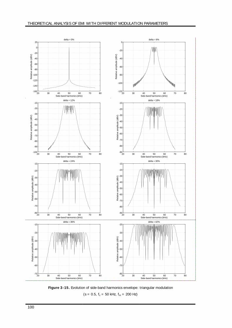
THEORETICAL ANALYSIS OF EMI WITH DIFFERENT MODULATION PARAMETERS
100
20 30 40 50 60 70 80-160
-140
-120
-100
-80
-60
-40
-20
0
20
Side-band harmonics (kHz)
Rel
ativ
e am
plitu
de (d
BV)
delta = 0%
20 30 40 50 60 70 80
-120
-100
-80
-60
-40
-20
0
Side-band harmonics (kHz)
Rel
ativ
e am
plitu
de (d
BV)
delta = 6%
20 30 40 50 60 70 80-100
-90
-80
-70
-60
-50
-40
-30
-20
-10
Side-band harmonics (kHz)
Rel
ativ
e am
plitu
de (d
BV)
delta = 12%
20 30 40 50 60 70 80
-90
-80
-70
-60
-50
-40
-30
-20
-10
Side-band harmonics (kHz)
Rel
ativ
e am
plitu
de (d
BV)
delta = 18%
20 30 40 50 60 70 80-80
-70
-60
-50
-40
-30
-20
-10
Side-band harmonics (kHz)
Rel
ativ
e am
plitu
de (d
BV)
delta = 24%
20 30 40 50 60 70 80
-90
-80
-70
-60
-50
-40
-30
-20
-10
Side-band harmonics (kHz)
Rel
ativ
e am
plitu
de (d
BV)
delta = 30%
20 30 40 50 60 70 80-70
-60
-50
-40
-30
-20
-10
Side-band harmonics (kHz)
Rel
ativ
e am
plitu
de (d
BV)
delta = 36%
20 30 40 50 60 70 80
-80
-70
-60
-50
-40
-30
-20
Side-band harmonics (kHz)
Rel
ativ
e am
plitu
de (d
BV)
delta = 42%
Figure 3-15. Evolution of side-band harmonics envelope: triangular modulation
(s = 0.5, fc = 50 kHz, fm = 200 Hz)
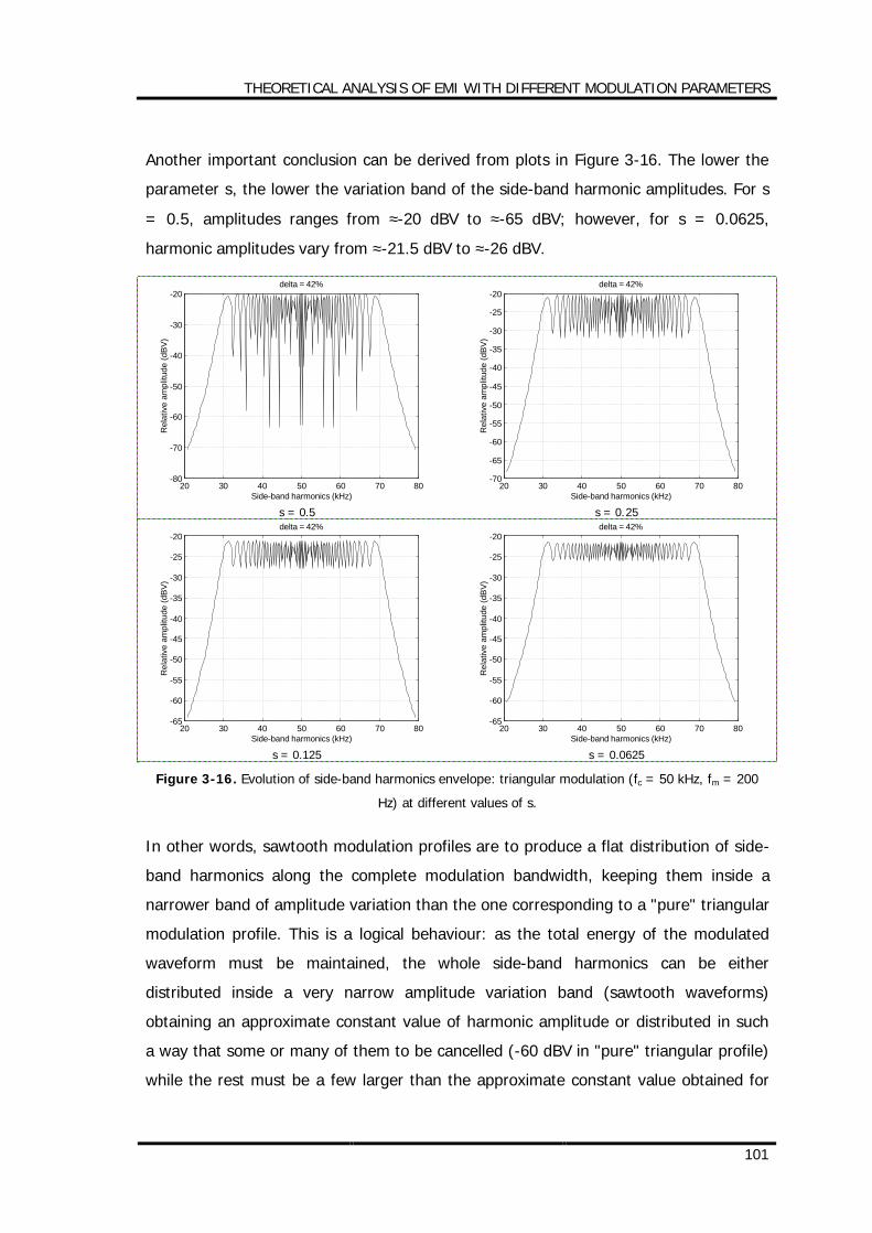
THEORETICAL ANALYSIS OF EMI WITH DIFFERENT MODULATION PARAMETERS
101
Another important conclusion can be derived from plots in Figure 3-16. The lower the
parameter s, the lower the variation band of the side-band harmonic amplitudes. For s
= 0.5, amplitudes ranges from ≈-20 dBV to ≈-65 dBV; however, for s = 0.0625,
harmonic amplitudes vary from ≈-21.5 dBV to ≈-26 dBV.
20 30 40 50 60 70 80-80
-70
-60
-50
-40
-30
-20
Side-band harmonics (kHz)
Rel
ativ
e am
plitu
de (d
BV)
delta = 42%
s = 0.5
20 30 40 50 60 70 80-70
-65
-60
-55
-50
-45
-40
-35
-30
-25
-20
Side-band harmonics (kHz)R
elat
ive
ampl
itude
(dBV
)
delta = 42%
s = 0.25
20 30 40 50 60 70 80-65
-60
-55
-50
-45
-40
-35
-30
-25
-20
Side-band harmonics (kHz)
Rel
ativ
e am
plitu
de (d
BV)
delta = 42%
s = 0.125
20 30 40 50 60 70 80-65
-60
-55
-50
-45
-40
-35
-30
-25
-20
Side-band harmonics (kHz)
Rel
ativ
e am
plitu
de (d
BV)
delta = 42%
s = 0.0625
Figure 3-16. Evolution of side-band harmonics envelope: triangular modulation (fc = 50 kHz, fm = 200
Hz) at different values of s.
In other words, sawtooth modulation profiles are to produce a flat distribution of side-
band harmonics along the complete modulation bandwidth, keeping them inside a
narrower band of amplitude variation than the one corresponding to a "pure" triangular
modulation profile. This is a logical behaviour: as the total energy of the modulated
waveform must be maintained, the whole side-band harmonics can be either
distributed inside a very narrow amplitude variation band (sawtooth waveforms)
obtaining an approximate constant value of harmonic amplitude or distributed in such
a way that some or many of them to be cancelled (-60 dBV in "pure" triangular profile)
while the rest must be a few larger than the approximate constant value obtained for
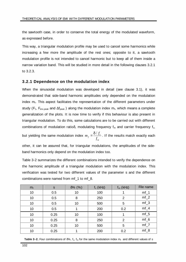
THEORETICAL ANALYSIS OF EMI WITH DIFFERENT MODULATION PARAMETERS
102
the sawtooth case, in order to conserve the total energy of the modulated waveform,
as expressed before.
This way, a triangular modulation profile may be used to cancel some harmonics while
increasing a few more the amplitude of the rest ones; opposite to it, a sawtooth
modulation profile is not intended to cancel harmonic but to keep all of them inside a
narrow variation band. This will be studied in more detail in the following clauses 3.2.1
to 3.2.3.
3.2.1 Dependence on the modulation index
When the sinusoidal modulation was developed in detail (see clause 3.1), it was
demonstrated that side-band harmonic amplitudes only depended on the modulation
index mf. This aspect facilitates the representation of the different parameters under
study (F1, Fenv,peak and ∆fpeak ) along the modulation index mf, which means a complete
generalization of the plots. It is now time to verify if this behaviour is also present in
triangular modulation. To do this, some calculations are to be carried out with different
combinations of modulation ratioδ, modulating frequency fm and carrier frequency fc,
but yielding the same modulation index m
cf f
fm ⋅=
δ. If the results match exactly each
other, it can be assured that, for triangular modulations, the amplitudes of the side-
band harmonics only depend on the modulation index too.
Table 3-2 summarizes the different combinations intended to verify the dependence on
the harmonic amplitude of a triangular modulation with the modulation index. This
verification was tested for two different values of the parameter s and the different
combinations were named from mf_1 to mf_8.
mf s δ% (%) fc (kHz) fm (kHz) File name
10 0.5 10 100 1 mf_1
10 0.5 8 250 2 mf_2
10 0.5 10 500 5 mf_3
10 0.5 1 200 0.2 mf_4
10 0.25 10 100 1 mf_5
10 0.25 8 250 2 mf_6
10 0.25 10 500 5 mf_7
10 0.25 1 200 0.2 mf_8
Table 3-2. Four combinations of δ%, fc, fm for the same modulation index mf and different values of s
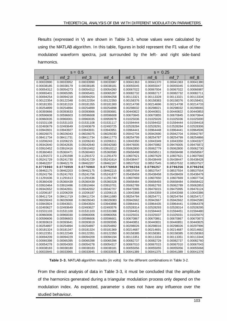
THEORETICAL ANALYSIS OF EMI WITH DIFFERENT MODULATION PARAMETERS
103
Results (expressed in V) are shown in Table 3-3, whose values were calculated by
using the MATLAB algorithm. In this table, figures in bold represent the F1 value of the
modulated waveform spectra, just surrounded by the left- and right side-band
harmonics.
s = 0.5 s = 0.25 mf_1 mf_2 mf_3 mf_4 mf_5 mf_6 mf_7 mf_8
0.00033990 0.00038185 0.00054312 0.00065401 0.00094254 0.00122354 0.00181355 0.00254899 0.00393666 0.00596608 0.00960035 0.01531108 0.02493679 0.03943931 0.06026075 0.08411734 0.10206243 0.09342640 0.03910452 0.05360463 0.11291572 0.05241729 0.08462207 0.0776960 0.08462175 0.05241756 0.11291636 0.05360439 0.03910464 0.09342652 0.10206187 0.08411724 0.06026043 0.03943924 0.02493627 0.01531103 0.00960006 0.00596606 0.00393619 0.00254897 0.00181324 0.00122351 0.00094209 0.00065398 0.00054278 0.00038183 0.00033945
0.00033952 0.00038179 0.00054273 0.00065395 0.00094218 0.00122348 0.00181319 0.00254894 0.00393633 0.00596603 0.00960001 0.01531103 0.02493649 0.03943927 0.06026043 0.08411731 0.10206215 0.09342635 0.03910416 0.05360471 0.11291598 0.05241730 0.08462179 0.0776959 0.08462203 0.05241763 0.11291613 0.05360439 0.03910496 0.09342651 0.10206209 0.08411719 0.06026068 0.03943921 0.02493649 0.01531100 0.00960030 0.00596603 0.00393641 0.00254894 0.00181347 0.00122349 0.00094229 0.00065395 0.00054300 0.00038180 0.00033965
0.00033990 0.00038185 0.00054312 0.00065401 0.00094254 0.00122354 0.00181355 0.00254899 0.00393666 0.00596608 0.00960035 0.01531108 0.02493679 0.03943931 0.06026075 0.08411734 0.10206243 0.09342640 0.03910452 0.05360463 0.11291572 0.05241729 0.08462207 0.0776960 0.08462175 0.05241756 0.11291636 0.05360439 0.03910464 0.09342652 0.10206187 0.08411724 0.06026043 0.03943924 0.02493627 0.01531103 0.00960006 0.00596606 0.00393619 0.00254897 0.00181324 0.00122351 0.00094209 0.00065398 0.00054278 0.00038183 0.00033945
0.00033987 0.00038181 0.00054260 0.00065397 0.00094258 0.00122350 0.00181300 0.00254898 0.00393681 0.00596608 0.00959978 0.01531117 0.02493725 0.03943951 0.06026030 0.08411773 0.10206311 0.09342580 0.03910212 0.05360580 0.11291470 0.05241614 0.08462167 0.0776959 0.08462215 0.05241877 0.11291740 0.05360328 0.03910701 0.09342707 0.10206115 0.08411680 0.06026083 0.03943898 0.02493576 0.01531088 0.00960056 0.00596601 0.00393595 0.00254892 0.00181369 0.00122350 0.00094194 0.00065396 0.00054317 0.00038181 0.00033935
0.00041363 0.00055045 0.00067022 0.00082732 0.00113321 0.00158376 0.00214708 0.00298032 0.00440822 0.00670845 0.01025036 0.01594444 0.02528284 0.03964441 0.05942704 0.08254799 0.10043350 0.09476005 0.05062800 0.05658498 0.10607621 0.05438447 0.08537532 0.0796256 0.08537554 0.05438459 0.10607669 0.05658484 0.05062789 0.09475995 0.10043368 0.08254784 0.05942662 0.03964441 0.02528314 0.01594451 0.01025031 0.00670867 0.00440851 0.00298026 0.00214687 0.00158385 0.00113351 0.00082737 0.00067010 0.00055056 0.00041389
0.00041370 0.00055047 0.00067004 0.00082717 0.00113328 0.00158383 0.00214696 0.00298021 0.00440831 0.00670855 0.01025026 0.01594432 0.02528291 0.03964448 0.05942690 0.08254787 0.10043349 0.09475982 0.05062779 0.05658511 0.10607629 0.05438449 0.08537545 0.0796257 0.08537547 0.05438458 0.10607650 0.05658493 0.05062793 0.09476015 0.10043359 0.08254771 0.05942667 0.03964435 0.02528293 0.01594443 0.01025037 0.00670861 0.00440831 0.00298016 0.00214691 0.00158381 0.00113334 0.00082729 0.00067015 0.00055055 0.00041375
0.00041363 0.00055045 0.00067022 0.00082732 0.00113321 0.00158376 0.00214708 0.00298032 0.00440822 0.00670845 0.01025036 0.01594444 0.02528284 0.03964441 0.05942704 0.08254799 0.10043350 0.09476005 0.05062800 0.05658498 0.10607621 0.05438447 0.08537532 0.0796256 0.08537554 0.05438459 0.10607669 0.05658484 0.05062789 0.09475995 0.10043368 0.08254784 0.05942662 0.03964441 0.02528314 0.01594451 0.01025031 0.00670867 0.00440851 0.00298026 0.00214687 0.00158385 0.00113351 0.00082737 0.00067010 0.00055056 0.00041389
0.00041380 0.00055035 0.00066987 0.00082711 0.00113334 0.00158401 0.00214733 0.00298065 0.00440853 0.00670844 0.01025000 0.01594418 0.02528306 0.03964506 0.05942787 0.08254866 0.10043327 0.09475872 0.05062730 0.05658567 0.10607560 0.05438428 0.08537527 0.0796256 0.08537554 0.05438479 0.10607734 0.05658422 0.05062853 0.09476124 0.10043386 0.08254717 0.05942580 0.03964378 0.02528295 0.01594480 0.01025070 0.00670873 0.00440825 0.00297996 0.00214662 0.00158363 0.00113344 0.00082760 0.00067043 0.00055068 0.00041378
Table 3-3. MATLAB algorithm results (in volts) for the different combinations in Table 3-2.
From the direct analysis of data in Table 3-3, it must be concluded that the amplitude
of the harmonics generated during a triangular modulation process only depend on the
modulation index. As expected, parameter s does not have any influence over the
studied behaviour.
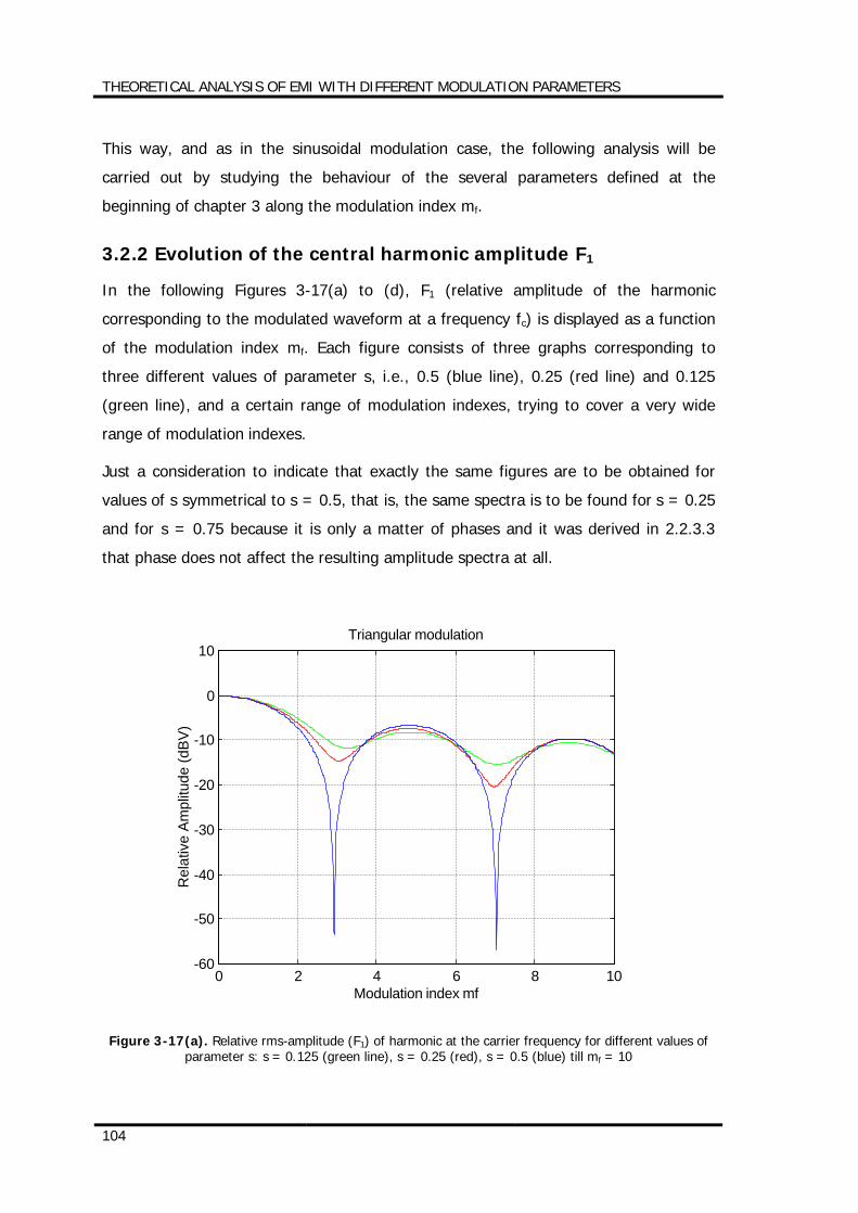
THEORETICAL ANALYSIS OF EMI WITH DIFFERENT MODULATION PARAMETERS
104
This way, and as in the sinusoidal modulation case, the following analysis will be
carried out by studying the behaviour of the several parameters defined at the
beginning of chapter 3 along the modulation index mf.
3.2.2 Evolution of the central harmonic amplitude F1
In the following Figures 3-17(a) to (d), F1 (relative amplitude of the harmonic
corresponding to the modulated waveform at a frequency fc) is displayed as a function
of the modulation index mf. Each figure consists of three graphs corresponding to
three different values of parameter s, i.e., 0.5 (blue line), 0.25 (red line) and 0.125
(green line), and a certain range of modulation indexes, trying to cover a very wide
range of modulation indexes.
Just a consideration to indicate that exactly the same figures are to be obtained for
values of s symmetrical to s = 0.5, that is, the same spectra is to be found for s = 0.25
and for s = 0.75 because it is only a matter of phases and it was derived in 2.2.3.3
that phase does not affect the resulting amplitude spectra at all.
0 2 4 6 8 10-60
-50
-40
-30
-20
-10
0
10
Modulation index mf
Rel
ativ
e Am
plitu
de (d
BV)
Triangular modulation
Figure 3-17(a). Relative rms-amplitude (F1) of harmonic at the carrier frequency for different values of parameter s: s = 0.125 (green line), s = 0.25 (red), s = 0.5 (blue) till mf = 10
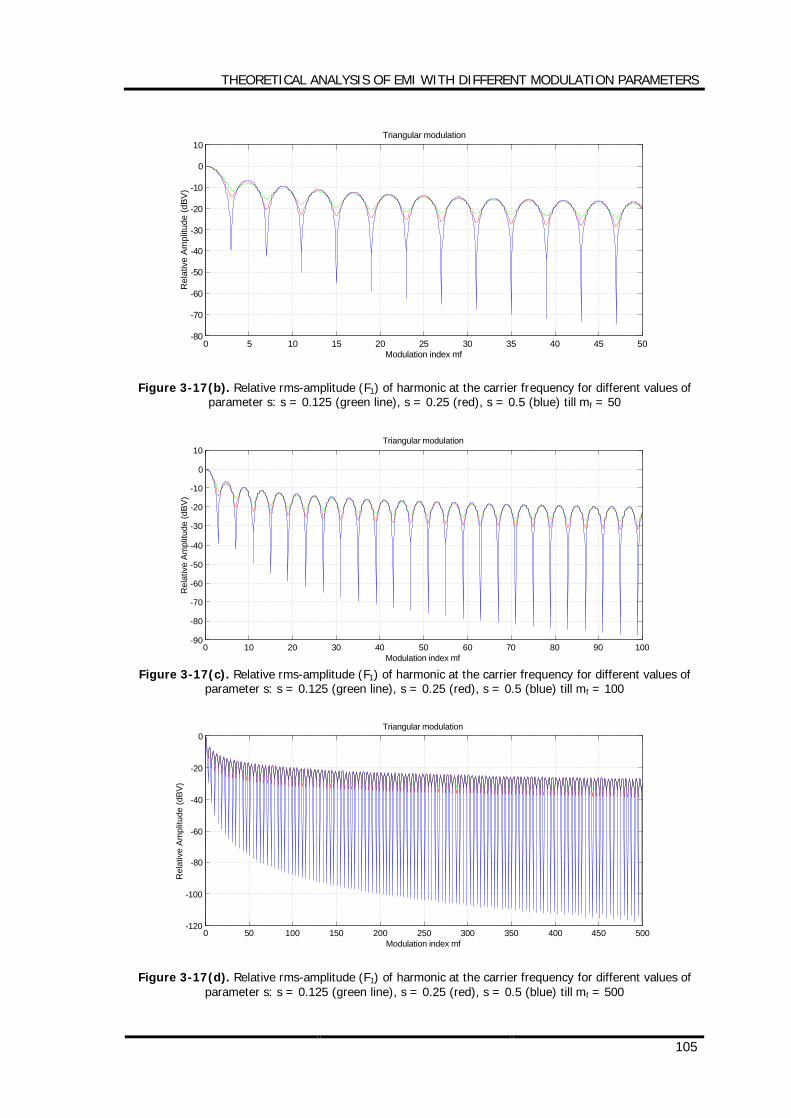
THEORETICAL ANALYSIS OF EMI WITH DIFFERENT MODULATION PARAMETERS
105
0 5 10 15 20 25 30 35 40 45 50-80
-70
-60
-50
-40
-30
-20
-10
0
10
Modulation index mf
Rel
ativ
e Am
plitu
de (d
BV)
Triangular modulation
Figure 3-17(b). Relative rms-amplitude (F1) of harmonic at the carrier frequency for different values of parameter s: s = 0.125 (green line), s = 0.25 (red), s = 0.5 (blue) till mf = 50
0 10 20 30 40 50 60 70 80 90 100-90
-80
-70
-60
-50
-40
-30
-20
-10
0
10
Modulation index mf
Rel
ativ
e A
mpl
itude
(dB
V)
Triangular modulation
Figure 3-17(c). Relative rms-amplitude (F1) of harmonic at the carrier frequency for different values of
parameter s: s = 0.125 (green line), s = 0.25 (red), s = 0.5 (blue) till mf = 100
0 50 100 150 200 250 300 350 400 450 500-120
-100
-80
-60
-40
-20
0
Modulation index mf
Rel
ativ
e Am
plitu
de (d
BV)
Triangular modulation
Figure 3-17(d). Relative rms-amplitude (F1) of harmonic at the carrier frequency for different values of parameter s: s = 0.125 (green line), s = 0.25 (red), s = 0.5 (blue) till mf = 500
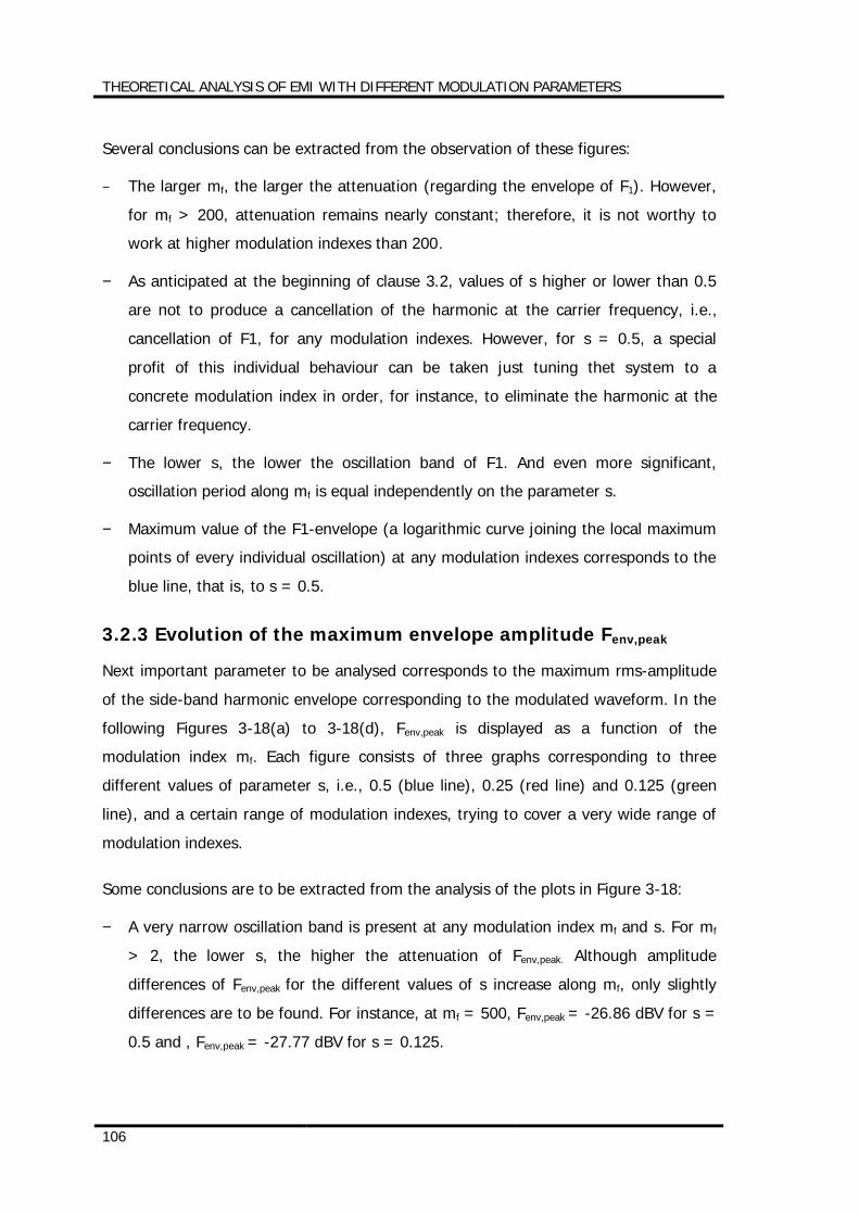
THEORETICAL ANALYSIS OF EMI WITH DIFFERENT MODULATION PARAMETERS
106
Several conclusions can be extracted from the observation of these figures:
− The larger mf, the larger the attenuation (regarding the envelope of F1). However,
for mf > 200, attenuation remains nearly constant; therefore, it is not worthy to
work at higher modulation indexes than 200.
− As anticipated at the beginning of clause 3.2, values of s higher or lower than 0.5
are not to produce a cancellation of the harmonic at the carrier frequency, i.e.,
cancellation of F1, for any modulation indexes. However, for s = 0.5, a special
profit of this individual behaviour can be taken just tuning thet system to a
concrete modulation index in order, for instance, to eliminate the harmonic at the
carrier frequency.
− The lower s, the lower the oscillation band of F1. And even more significant,
oscillation period along mf is equal independently on the parameter s.
− Maximum value of the F1-envelope (a logarithmic curve joining the local maximum
points of every individual oscillation) at any modulation indexes corresponds to the
blue line, that is, to s = 0.5.
3.2.3 Evolution of the maximum envelope amplitude Fenv,peak
Next important parameter to be analysed corresponds to the maximum rms-amplitude
of the side-band harmonic envelope corresponding to the modulated waveform. In the
following Figures 3-18(a) to 3-18(d), Fenv,peak is displayed as a function of the
modulation index mf. Each figure consists of three graphs corresponding to three
different values of parameter s, i.e., 0.5 (blue line), 0.25 (red line) and 0.125 (green
line), and a certain range of modulation indexes, trying to cover a very wide range of
modulation indexes.
Some conclusions are to be extracted from the analysis of the plots in Figure 3-18:
− A very narrow oscillation band is present at any modulation index mf and s. For mf
> 2, the lower s, the higher the attenuation of Fenv,peak. Although amplitude
differences of Fenv,peak for the different values of s increase along mf, only slightly
differences are to be found. For instance, at mf = 500, Fenv,peak = -26.86 dBV for s =
0.5 and , Fenv,peak = -27.77 dBV for s = 0.125.
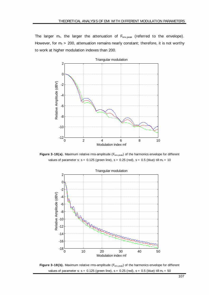
THEORETICAL ANALYSIS OF EMI WITH DIFFERENT MODULATION PARAMETERS
107
The larger mf, the larger the attenuation of Fenv,peak (referred to the envelope).
However, for mf > 200, attenuation remains nearly constant; therefore, it is not worthy
to work at higher modulation indexes than 200.
0 2 4 6 8 10-12
-10
-8
-6
-4
-2
0
2
Modulation index mf
Rel
ativ
e Am
plitu
de (d
BV)
Triangular modulation
Figure 3-18(a). Maximum relative rms-amplitude (Fenv,peak) of the harmonics envelope for different
values of parameter s: s = 0.125 (green line), s = 0.25 (red), s = 0.5 (blue) till mf = 10
0 10 20 30 40 50-18
-16
-14
-12
-10
-8
-6
-4
-2
0
2
Modulation index mf
Rel
ativ
e Am
plitu
de (d
BV)
Triangular modulation
Figure 3-18(b). Maximum relative rms-amplitude (Fenv,peak) of the harmonics envelope for different
values of parameter s: s = 0.125 (green line), s = 0.25 (red), s = 0.5 (blue) till mf = 50
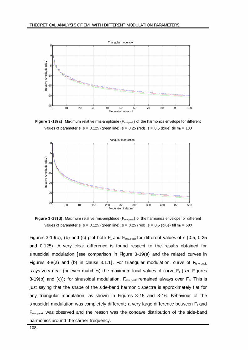
THEORETICAL ANALYSIS OF EMI WITH DIFFERENT MODULATION PARAMETERS
108
0 10 20 30 40 50 60 70 80 90 100-25
-20
-15
-10
-5
0
5
Modulation index mf
Rel
ativ
e Am
plitu
de (d
BV)
Triangular modulation
Figure 3-18(c). Maximum relative rms-amplitude (Fenv,peak) of the harmonics envelope for different
values of parameter s: s = 0.125 (green line), s = 0.25 (red), s = 0.5 (blue) till mf = 100
0 50 100 150 200 250 300 350 400 450 500-30
-25
-20
-15
-10
-5
0
Modulation index mf
Rel
ativ
e Am
plitu
de (d
BV)
Triangular modulation
Figure 3-18(d). Maximum relative rms-amplitude (Fenv,peak) of the harmonics envelope for different
values of parameter s: s = 0.125 (green line), s = 0.25 (red), s = 0.5 (blue) till mf = 500
Figures 3-19(a), (b) and (c) plot both F1 and Fenv,peak for different values of s (0.5, 0.25
and 0.125). A very clear difference is found respect to the results obtained for
sinusoidal modulation [see comparison in Figure 3-19(a) and the related curves in
Figures 3-8(a) and (b) in clause 3.1.1]. For triangular modulation, curve of Fenv,peak
stays very near (or even matches) the maximum local values of curve F1 (see Figures
3-19(b) and (c)); for sinusoidal modulation, Fenv,peak remained always over F1. This is
just saying that the shape of the side-band harmonic spectra is approximately flat for
any triangular modulation, as shown in Figures 3-15 and 3-16. Behaviour of the
sinusoidal modulation was completely different; a very large difference between F1 and
Fenv,peak was observed and the reason was the concave distribution of the side-band
harmonics around the carrier frequency.
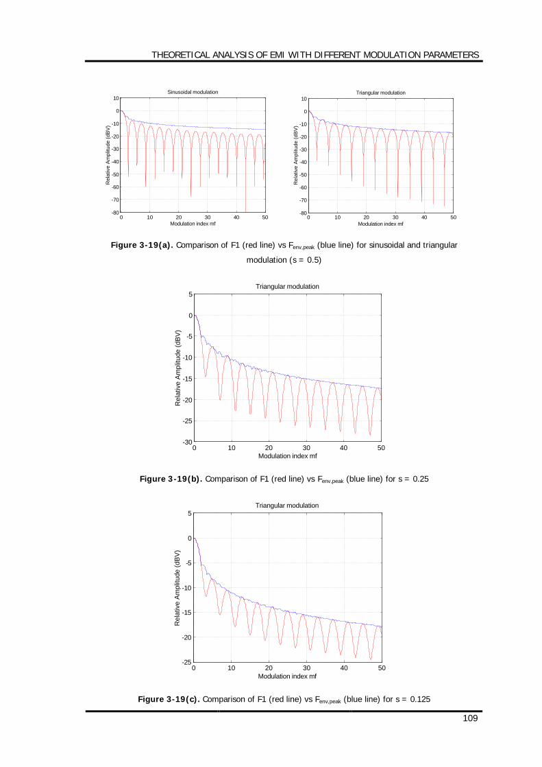
THEORETICAL ANALYSIS OF EMI WITH DIFFERENT MODULATION PARAMETERS
109
0 10 20 30 40 50-80
-70
-60
-50
-40
-30
-20
-10
0
10
Modulation index mf
Rel
ativ
e Am
plitu
de (d
BV)
Sinusoidal modulation
0 10 20 30 40 50-80
-70
-60
-50
-40
-30
-20
-10
0
10
Modulation index mf
Rel
ativ
e A
mpl
itude
(dB
V)
Triangular modulation
Figure 3-19(a). Comparison of F1 (red line) vs Fenv,peak (blue line) for sinusoidal and triangular
modulation (s = 0.5)
0 10 20 30 40 50-30
-25
-20
-15
-10
-5
0
5
Modulation index mf
Rel
ativ
e Am
plitu
de (d
BV)
Triangular modulation
Figure 3-19(b). Comparison of F1 (red line) vs Fenv,peak (blue line) for s = 0.25
0 10 20 30 40 50-25
-20
-15
-10
-5
0
5
Modulation index mf
Rel
ativ
e Am
plitu
de (d
BV)
Triangular modulation
Figure 3-19(c). Comparison of F1 (red line) vs Fenv,peak (blue line) for s = 0.125
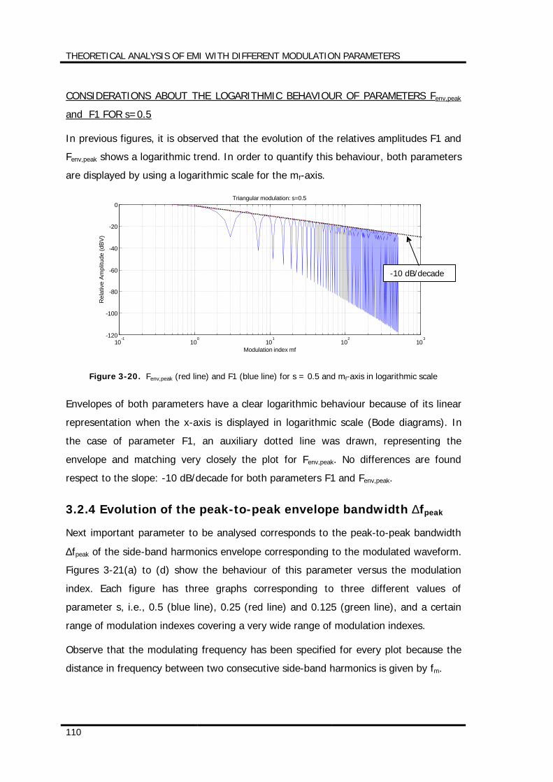
THEORETICAL ANALYSIS OF EMI WITH DIFFERENT MODULATION PARAMETERS
110
CONSIDERATIONS ABOUT THE LOGARITHMIC BEHAVIOUR OF PARAMETERS Fenv,peak
and F1 FOR s=0.5
In previous figures, it is observed that the evolution of the relatives amplitudes F1 and
Fenv,peak shows a logarithmic trend. In order to quantify this behaviour, both parameters
are displayed by using a logarithmic scale for the mf-axis.
10
-110
010
110
210
3-120
-100
-80
-60
-40
-20
0
Modulation index mf
Rel
ativ
e Am
plitu
de (d
BV)
Triangular modulation: s=0.5
Figure 3-20. Fenv,peak (red line) and F1 (blue line) for s = 0.5 and mf-axis in logarithmic scale
Envelopes of both parameters have a clear logarithmic behaviour because of its linear
representation when the x-axis is displayed in logarithmic scale (Bode diagrams). In
the case of parameter F1, an auxiliary dotted line was drawn, representing the
envelope and matching very closely the plot for Fenv,peak. No differences are found
respect to the slope: -10 dB/decade for both parameters F1 and Fenv,peak.
3.2.4 Evolution of the peak-to-peak envelope bandwidth ∆fpeak
Next important parameter to be analysed corresponds to the peak-to-peak bandwidth
∆fpeak of the side-band harmonics envelope corresponding to the modulated waveform.
Figures 3-21(a) to (d) show the behaviour of this parameter versus the modulation
index. Each figure has three graphs corresponding to three different values of
parameter s, i.e., 0.5 (blue line), 0.25 (red line) and 0.125 (green line), and a certain
range of modulation indexes covering a very wide range of modulation indexes.
Observe that the modulating frequency has been specified for every plot because the
distance in frequency between two consecutive side-band harmonics is given by fm.
-10 dB/decade
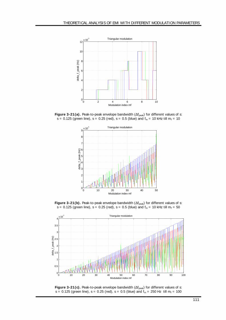
THEORETICAL ANALYSIS OF EMI WITH DIFFERENT MODULATION PARAMETERS
111
0 2 4 6 8 100
2
4
6
8
10
12x 10
4
Modulation index mf
delta
_f_p
eak
(Hz)
Triangular modulation
Figure 3-21(a). Peak-to-peak envelope bandwidth (∆fpeak) for different values of s: s = 0.125 (green line), s = 0.25 (red), s = 0.5 (blue) and fm = 10 kHz till mf = 10
0 10 20 30 40 500
1
2
3
4
5
6
7
8
9x 10
5
Modulation index mf
delta
_f_p
eak
(Hz)
Triangular modulation
Figure 3-21(b). Peak-to-peak envelope bandwidth (∆fpeak) for different values of s: s = 0.125 (green line), s = 0.25 (red), s = 0.5 (blue) and fm = 10 kHz till mf = 50
0 10 20 30 40 50 60 70 80 90 1000
0.5
1
1.5
2
2.5
3
3.5
4x 10
4
Modulation index mf
delta
_f_p
eak
(Hz)
Triangular modulation
Figure 3-21(c). Peak-to-peak envelope bandwidth (∆fpeak) for different values of s: s = 0.125 (green line), s = 0.25 (red), s = 0.5 (blue) and fm = 250 Hz till mf = 100
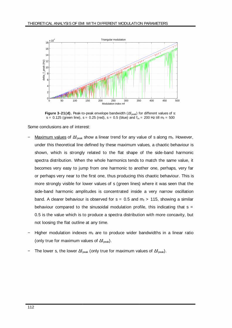
THEORETICAL ANALYSIS OF EMI WITH DIFFERENT MODULATION PARAMETERS
112
0 50 100 150 200 250 300 350 400 450 5000
2
4
6
8
10
12
14
16
18x 104
Modulation index mf
delta
_f_p
eak
(Hz)
Triangular modulation
Figure 3-21(d). Peak-to-peak envelope bandwidth (∆fpeak) for different values of s: s = 0.125 (green line), s = 0.25 (red), s = 0.5 (blue) and fm = 200 Hz till mf = 500
Some conclusions are of interest:
− Maximum values of ∆fpeak show a linear trend for any value of s along mf. However,
under this theoretical line defined by these maximum values, a chaotic behaviour is
shown, which is strongly related to the flat shape of the side-band harmonic
spectra distribution. When the whole harmonics tends to match the same value, it
becomes very easy to jump from one harmonic to another one, perhaps, very far
or perhaps very near to the first one, thus producing this chaotic behaviour. This is
more strongly visible for lower values of s (green lines) where it was seen that the
side-band harmonic amplitudes is concentrated inside a very narrow oscillation
band. A clearer behaviour is observed for s = 0.5 and mf > 115, showing a similar
behaviour compared to the sinusoidal modulation profile, this indicating that s =
0.5 is the value which is to produce a spectra distribution with more concavity, but
not loosing the flat outline at any time.
− Higher modulation indexes mf are to produce wider bandwidths in a linear ratio
(only true for maximum values of ∆fpeak).
− The lower s, the lower ∆fpeak (only true for maximum values of ∆fpeak).
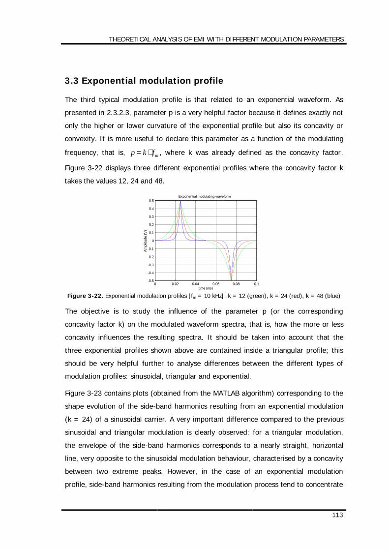
THEORETICAL ANALYSIS OF EMI WITH DIFFERENT MODULATION PARAMETERS
113
3.3 Exponential modulation profile
The third typical modulation profile is that related to an exponential waveform. As
presented in 2.3.2.3, parameter p is a very helpful factor because it defines exactly not
only the higher or lower curvature of the exponential profile but also its concavity or
convexity. It is more useful to declare this parameter as a function of the modulating
frequency, that is, mfkp ⋅= , where k was already defined as the concavity factor.
Figure 3-22 displays three different exponential profiles where the concavity factor k
takes the values 12, 24 and 48.
0 0.02 0.04 0.06 0.08 0.1-0.5
-0.4
-0.3
-0.2
-0.1
0
0.1
0.2
0.3
0.4
0.5
time (ms)
Ampl
itude
(V)
Exponential modulating waveform
Figure 3-22. Exponential modulation profiles [fm = 10 kHz]: k = 12 (green), k = 24 (red), k = 48 (blue)
The objective is to study the influence of the parameter p (or the corresponding
concavity factor k) on the modulated waveform spectra, that is, how the more or less
concavity influences the resulting spectra. It should be taken into account that the
three exponential profiles shown above are contained inside a triangular profile; this
should be very helpful further to analyse differences between the different types of
modulation profiles: sinusoidal, triangular and exponential.
Figure 3-23 contains plots (obtained from the MATLAB algorithm) corresponding to the
shape evolution of the side-band harmonics resulting from an exponential modulation
(k = 24) of a sinusoidal carrier. A very important difference compared to the previous
sinusoidal and triangular modulation is clearly observed: for a triangular modulation,
the envelope of the side-band harmonics corresponds to a nearly straight, horizontal
line, very opposite to the sinusoidal modulation behaviour, characterised by a concavity
between two extreme peaks. However, in the case of an exponential modulation
profile, side-band harmonics resulting from the modulation process tend to concentrate
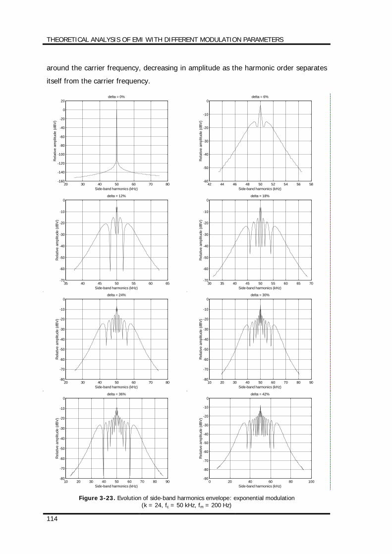
THEORETICAL ANALYSIS OF EMI WITH DIFFERENT MODULATION PARAMETERS
114
around the carrier frequency, decreasing in amplitude as the harmonic order separates
itself from the carrier frequency.
20 30 40 50 60 70 80-160
-140
-120
-100
-80
-60
-40
-20
0
20
Side-band harmonics (kHz)
Rel
ativ
e am
plitu
de (d
BV)
delta = 0%
42 44 46 48 50 52 54 56 58
-60
-50
-40
-30
-20
-10
0
Side-band harmonics (kHz)
Rel
ativ
e am
plitu
de (d
BV)
delta = 6%
35 40 45 50 55 60 65-70
-60
-50
-40
-30
-20
-10
0
Side-band harmonics (kHz)
Rel
ativ
e am
plitu
de (d
BV)
delta = 12%
30 35 40 45 50 55 60 65 70
-70
-60
-50
-40
-30
-20
-10
0
Side-band harmonics (kHz)
Rel
ativ
e am
plitu
de (d
BV)
delta = 18%
20 30 40 50 60 70 80-80
-70
-60
-50
-40
-30
-20
-10
0
Side-band harmonics (kHz)
Rel
ativ
e am
plitu
de (d
BV)
delta = 24%
10 20 30 40 50 60 70 80 90
-80
-70
-60
-50
-40
-30
-20
-10
0
Side-band harmonics (kHz)
Rel
ativ
e am
plitu
de (d
BV)
delta = 30%
10 20 30 40 50 60 70 80 90-80
-70
-60
-50
-40
-30
-20
-10
0
Side-band harmonics (kHz)
Rel
ativ
e am
plitu
de (d
BV)
delta = 36%
0 20 40 60 80 100
-90
-80
-70
-60
-50
-40
-30
-20
-10
0
Side-band harmonics (kHz)
Rel
ativ
e am
plitu
de (d
BV)
delta = 42%
Figure 3-23. Evolution of side-band harmonics envelope: exponential modulation
(k = 24, fc = 50 kHz, fm = 200 Hz)
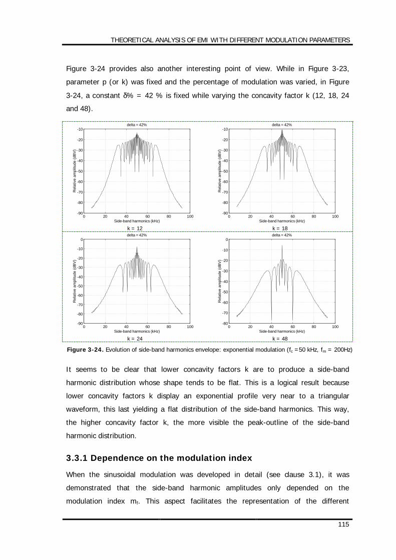
THEORETICAL ANALYSIS OF EMI WITH DIFFERENT MODULATION PARAMETERS
115
Figure 3-24 provides also another interesting point of view. While in Figure 3-23,
parameter p (or k) was fixed and the percentage of modulation was varied, in Figure
3-24, a constant δ% = 42 % is fixed while varying the concavity factor k (12, 18, 24
and 48).
0 20 40 60 80 100-90
-80
-70
-60
-50
-40
-30
-20
-10
Side-band harmonics (kHz)
Rel
ativ
e am
plitu
de (d
BV)
delta = 42%
k = 12
0 20 40 60 80 100-90
-80
-70
-60
-50
-40
-30
-20
-10
Side-band harmonics (kHz)R
elat
ive
ampl
itude
(dBV
)
delta = 42%
k = 18
0 20 40 60 80 100-90
-80
-70
-60
-50
-40
-30
-20
-10
0
Side-band harmonics (kHz)
Rel
ativ
e am
plitu
de (d
BV)
delta = 42%
k = 24
0 20 40 60 80 100-80
-70
-60
-50
-40
-30
-20
-10
0
Side-band harmonics (kHz)
Rel
ativ
e am
plitu
de (d
BV)
delta = 42%
k = 48
Figure 3-24. Evolution of side-band harmonics envelope: exponential modulation (fc =50 kHz, fm = 200Hz)
It seems to be clear that lower concavity factors k are to produce a side-band
harmonic distribution whose shape tends to be flat. This is a logical result because
lower concavity factors k display an exponential profile very near to a triangular
waveform, this last yielding a flat distribution of the side-band harmonics. This way,
the higher concavity factor k, the more visible the peak-outline of the side-band
harmonic distribution.
3.3.1 Dependence on the modulation index
When the sinusoidal modulation was developed in detail (see clause 3.1), it was
demonstrated that the side-band harmonic amplitudes only depended on the
modulation index mf. This aspect facilitates the representation of the different
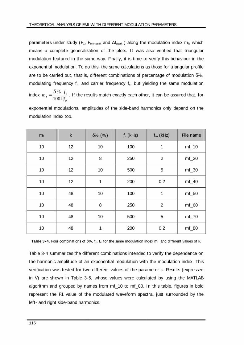
THEORETICAL ANALYSIS OF EMI WITH DIFFERENT MODULATION PARAMETERS
116
parameters under study (F1, Fenv,peak and ∆fpeak ) along the modulation index mf, which
means a complete generalization of the plots. It was also verified that triangular
modulation featured in the same way. Finally, it is time to verify this behaviour in the
exponential modulation. To do this, the same calculations as those for triangular profile
are to be carried out, that is, different combinations of percentage of modulation δ%,
modulating frequency fm and carrier frequency fc, but yielding the same modulation
index m
cf f
fm⋅⋅
=100
%δ. If the results match exactly each other, it can be assured that, for
exponential modulations, amplitudes of the side-band harmonics only depend on the
modulation index too.
mf k δ% (%) fc (kHz) fm (kHz) File name
10 12 10 100 1 mf_10
10 12 8 250 2 mf_20
10 12 10 500 5 mf_30
10 12 1 200 0.2 mf_40
10 48 10 100 1 mf_50
10 48 8 250 2 mf_60
10 48 10 500 5 mf_70
10 48 1 200 0.2 mf_80
Table 3-4. Four combinations of δ%, fc, fm for the same modulation index mf and different values of k.
Table 3-4 summarizes the different combinations intended to verify the dependence on
the harmonic amplitude of an exponential modulation with the modulation index. This
verification was tested for two different values of the parameter k. Results (expressed
in V) are shown in Table 3-5, whose values were calculated by using the MATLAB
algorithm and grouped by names from mf_10 to mf_80. In this table, figures in bold
represent the F1 value of the modulated waveform spectra, just surrounded by the
left- and right side-band harmonics.
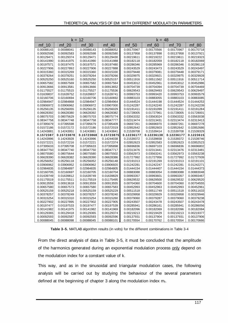
THEORETICAL ANALYSIS OF EMI WITH DIFFERENT MODULATION PARAMETERS
117
k = 12 k = 48 mf_10 mf_20 mf_30 mf_40 mf_50 mf_60 mf_70 mf_80
0.00088143 0.00092598 0.00129471 0.00141990 0.00197571 0.00227906 0.00315360 0.00378264 0.00525250 0.00657582 0.00913666 0.01175527 0.01639837 0.02160706 0.02984947 0.03906972 0.05256135 0.06628392 0.08075703 0.08347758 0.07395679 0.01572186 0.14243881 0.1572387 0.14243996 0.01572221 0.07395633 0.08347750 0.08075580 0.06628390 0.05256052 0.03906962 0.02984835 0.02160705 0.01639749 0.01175519 0.00913559 0.00657580 0.00525159 0.00378257 0.00315254 0.00227902 0.00197477 0.00141982 0.00129365 0.00092593 0.00088045
0.00088041 0.00092583 0.00129374 0.00141975 0.00197475 0.00227892 0.00315269 0.00378251 0.00525160 0.00657569 0.00913581 0.01175515 0.01639752 0.02160694 0.02984868 0.03906962 0.05256055 0.06628380 0.08075629 0.08347748 0.07395598 0.01572172 0.14243951
0.15723878 0.14243928 0.01572216 0.07395708 0.08347740 0.08075644 0.06628382 0.05256118 0.03906952 0.02984897 0.02160697 0.01639812 0.01175511 0.00913618 0.00657573 0.00525218 0.00378249 0.00315310 0.00227895 0.00197533 0.00141975 0.00129418 0.00092587 0.00088098
0.00088143 0.00092598 0.00129471 0.00141990 0.00197571 0.00227906 0.00315360 0.00378264 0.00525250 0.00657582 0.00913666 0.01175527 0.01639837 0.02160706 0.02984947 0.03906972 0.05256135 0.06628392 0.08075703 0.08347758 0.07395679 0.01572186 0.14243881
0.15723868 0.14243996 0.01572221 0.07395633 0.08347750 0.08075580 0.06628390 0.05256052 0.03906962 0.02984835 0.02160705 0.01639749 0.01175519 0.00913559 0.00657580 0.00525159 0.00378257 0.00315254 0.00227902 0.00197477 0.00141982 0.00129365 0.00092593 0.00088045
0.00088052 0.00092580 0.00129430 0.00141988 0.00197480 0.00227888 0.00315330 0.00378266 0.00525157 0.00657564 0.00913652 0.01175536 0.01639741 0.02160692 0.02984964 0.03907000 0.05256029 0.06628382 0.08075774 0.08347777 0.07395409 0.01572019 0.14243841
0.15723875 0.14244038 0.01572374 0.07395898 0.08347717 0.08075502 0.06628386 0.05256148 0.03906920 0.02984805 0.02160704 0.01639829 0.01175495 0.00913555 0.00657583 0.00525229 0.00378240 0.00315260 0.00227905 0.00197539 0.00141969 0.00129374 0.00092596 0.00088101
0.00170967 0.00137958 0.00219611 0.00182118 0.00286346 0.00243529 0.00379448 0.00329975 0.00511916 0.00453012 0.00704739 0.00629543 0.00993753 0.00883103 0.01444524 0.01242287 0.02191411 0.01728005 0.03563332 0.02313474 0.06697261 0.02852642 0.21539708
0.12236177 0.21539372 0.02852623 0.06696836 0.02313476 0.03562973 0.01727992 0.02191013 0.01242281 0.01444154 0.00883088 0.00993357 0.00629532 0.00704360 0.00452993 0.00511518 0.00329958 0.00379060 0.00243507 0.00285941 0.00182096 0.00219213 0.00137931 0.00170554
0.00170566 0.00137898 0.00219222 0.00182059 0.00285969 0.00243473 0.00379081 0.00329921 0.00511562 0.00452961 0.00704394 0.00629493 0.00993420 0.00883055 0.01444198 0.01242240 0.02191099 0.01727961 0.03563024 0.02313431 0.06696970 0.02852603 0.21539414
0.12236138 0.21539658 0.02852583 0.06697103 0.02313441 0.03563241 0.01727956 0.02191269 0.01242247 0.01444407 0.00883054 0.00993601 0.00629500 0.00704600 0.00452963 0.00511749 0.00329929 0.00379287 0.00243478 0.00286161 0.00182069 0.00219429 0.00137904 0.00170762
0.00170967 0.00137958 0.00219611 0.00182118 0.00286346 0.00243529 0.00379448 0.00329975 0.00511916 0.00453012 0.00704739 0.00629543 0.00993753 0.00883103 0.01444524 0.01242287 0.02191411 0.01728005 0.03563332 0.02313474 0.06697261 0.02852642 0.21539708
0.12236177 0.21539372 0.02852623 0.06696836 0.02313476 0.03562973 0.01727992 0.02191013 0.01242281 0.01444154 0.00883088 0.00993357 0.00629532 0.00704360 0.00452993 0.00511518 0.00329958 0.00379060 0.00243507 0.00285941 0.00182096 0.00219213 0.00137931 0.00170554
0.00170718 0.00137921 0.00219323 0.00182069 0.00286119 0.00243497 0.00379171 0.00329928 0.00511714 0.00452986 0.00704469 0.00629497 0.00993579 0.00883085 0.01444253 0.01242239 0.02191284 0.01728001 0.03563038 0.02313413 0.06697278 0.02852686 0.21539329 0.1223615 0.21539746 0.02852523 0.06696802 0.02313481 0.03563238 0.01727939 0.02191101 0.01242271 0.01444373 0.00883048 0.00993467 0.00629520 0.00704555 0.00452961 0.00511633 0.00329946 0.00379238 0.00243478 0.00286056 0.00182084 0.00219377 0.00137906 0.00170666
Table 3-5. MATLAB algorithm results (in volts) for the different combinations in Table 3-4
From the direct analysis of data in Table 3-5, it must be concluded that the amplitude
of the harmonics generated during an exponential modulation process only depend on
the modulation index for a constant value of k.
This way, and as in the sinusoidal and triangular modulation cases, the following
analysis will be carried out by studying the behaviour of the several parameters
defined at the beginning of chapter 3 along the modulation index mf.
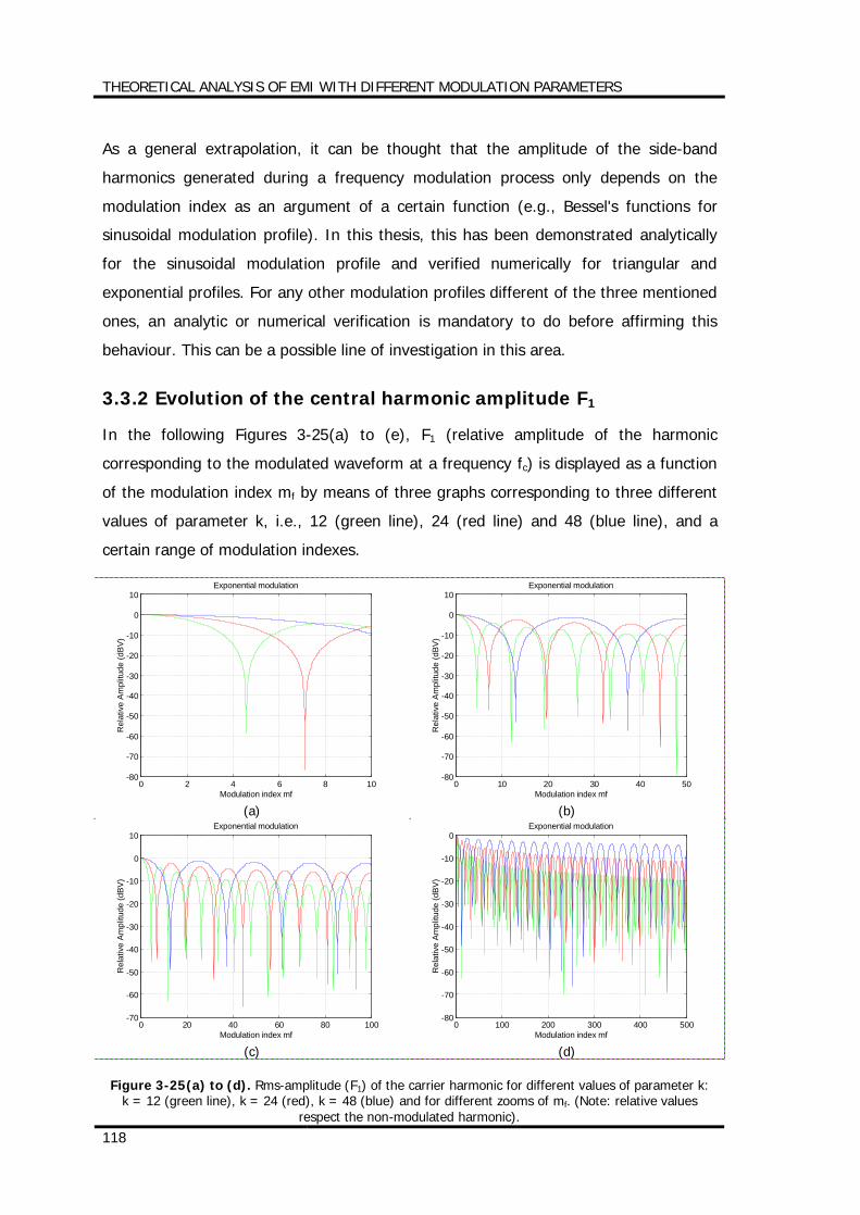
THEORETICAL ANALYSIS OF EMI WITH DIFFERENT MODULATION PARAMETERS
118
As a general extrapolation, it can be thought that the amplitude of the side-band
harmonics generated during a frequency modulation process only depends on the
modulation index as an argument of a certain function (e.g., Bessel's functions for
sinusoidal modulation profile). In this thesis, this has been demonstrated analytically
for the sinusoidal modulation profile and verified numerically for triangular and
exponential profiles. For any other modulation profiles different of the three mentioned
ones, an analytic or numerical verification is mandatory to do before affirming this
behaviour. This can be a possible line of investigation in this area.
3.3.2 Evolution of the central harmonic amplitude F1
In the following Figures 3-25(a) to (e), F1 (relative amplitude of the harmonic
corresponding to the modulated waveform at a frequency fc) is displayed as a function
of the modulation index mf by means of three graphs corresponding to three different
values of parameter k, i.e., 12 (green line), 24 (red line) and 48 (blue line), and a
certain range of modulation indexes.
0 2 4 6 8 10-80
-70
-60
-50
-40
-30
-20
-10
0
10
Modulation index mf
Rel
ativ
e Am
plitu
de (d
BV)
Exponential modulation
(a)
0 10 20 30 40 50-80
-70
-60
-50
-40
-30
-20
-10
0
10
Modulation index mf
Rel
ativ
e Am
plitu
de (d
BV)
Exponential modulation
(b)
0 20 40 60 80 100-70
-60
-50
-40
-30
-20
-10
0
10
Modulation index mf
Rel
ativ
e Am
plitu
de (d
BV)
Exponential modulation
(c)
0 100 200 300 400 500-80
-70
-60
-50
-40
-30
-20
-10
0
Modulation index mf
Rel
ativ
e Am
plitu
de (d
BV)
Exponential modulation
(d)
Figure 3-25(a) to (d). Rms-amplitude (F1) of the carrier harmonic for different values of parameter k: k = 12 (green line), k = 24 (red), k = 48 (blue) and for different zooms of mf. (Note: relative values
respect the non-modulated harmonic).
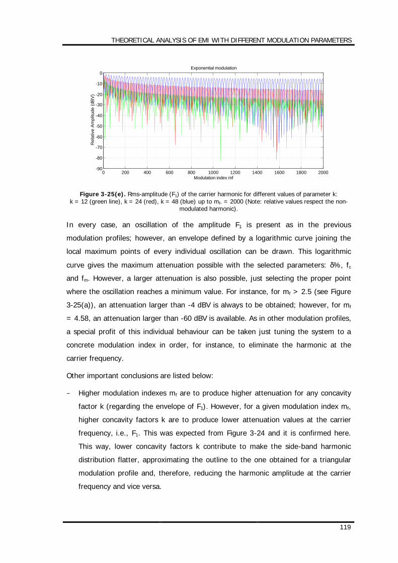
THEORETICAL ANALYSIS OF EMI WITH DIFFERENT MODULATION PARAMETERS
119
0 200 400 600 800 1000 1200 1400 1600 1800 2000-90
-80
-70
-60
-50
-40
-30
-20
-10
0
Modulation index mf
Rel
ativ
e Am
plitu
de (d
BV)
Exponential modulation
Figure 3-25(e). Rms-amplitude (F1) of the carrier harmonic for different values of parameter k: k = 12 (green line), k = 24 (red), k = 48 (blue) up to mf. = 2000 (Note: relative values respect the non-
modulated harmonic).
In every case, an oscillation of the amplitude F1 is present as in the previous
modulation profiles; however, an envelope defined by a logarithmic curve joining the
local maximum points of every individual oscillation can be drawn. This logarithmic
curve gives the maximum attenuation possible with the selected parameters: δ%, fc
and fm. However, a larger attenuation is also possible, just selecting the proper point
where the oscillation reaches a minimum value. For instance, for mf > 2.5 (see Figure
3-25(a)), an attenuation larger than -4 dBV is always to be obtained; however, for mf
= 4.58, an attenuation larger than -60 dBV is available. As in other modulation profiles,
a special profit of this individual behaviour can be taken just tuning the system to a
concrete modulation index in order, for instance, to eliminate the harmonic at the
carrier frequency.
Other important conclusions are listed below:
− Higher modulation indexes mf are to produce higher attenuation for any concavity
factor k (regarding the envelope of F1). However, for a given modulation index mf,
higher concavity factors k are to produce lower attenuation values at the carrier
frequency, i.e., F1. This was expected from Figure 3-24 and it is confirmed here.
This way, lower concavity factors k contribute to make the side-band harmonic
distribution flatter, approximating the outline to the one obtained for a triangular
modulation profile and, therefore, reducing the harmonic amplitude at the carrier
frequency and vice versa.
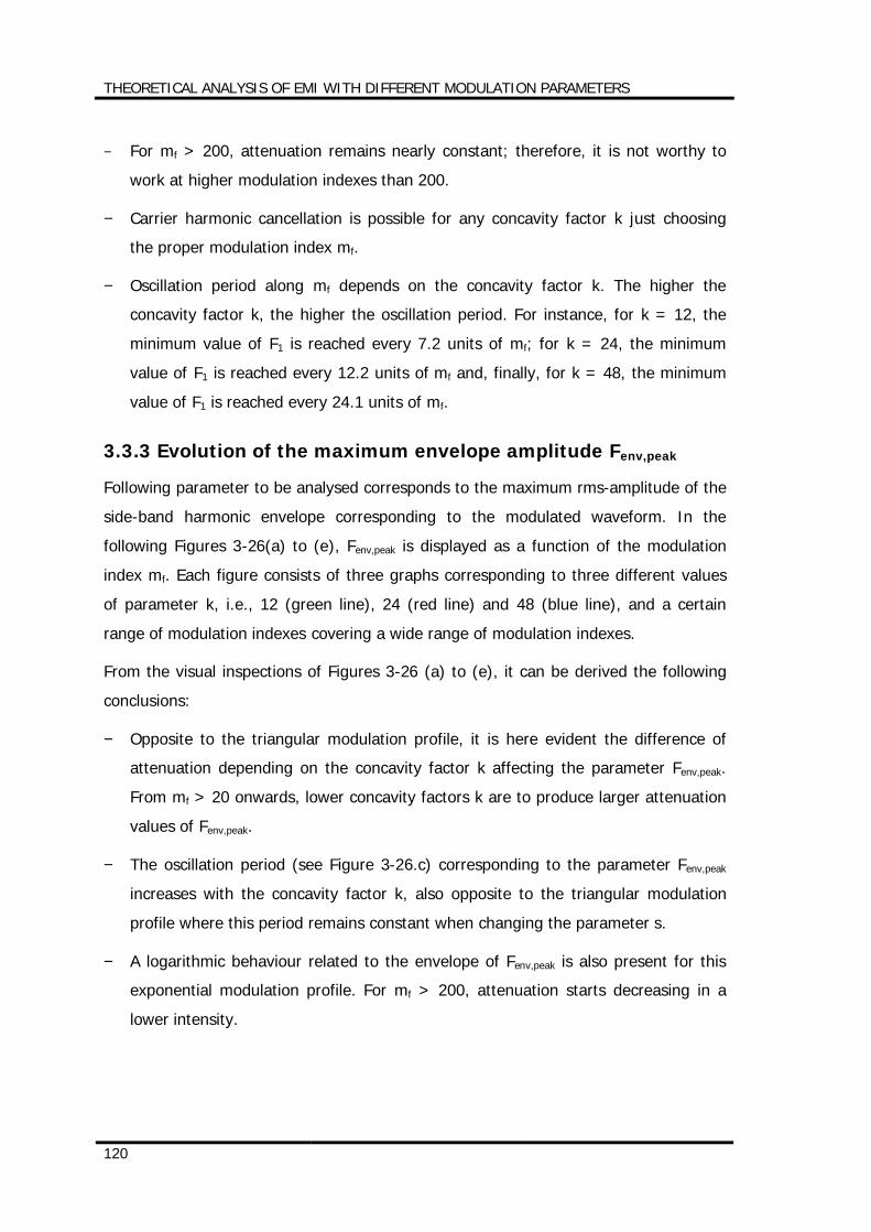
THEORETICAL ANALYSIS OF EMI WITH DIFFERENT MODULATION PARAMETERS
120
− For mf > 200, attenuation remains nearly constant; therefore, it is not worthy to
work at higher modulation indexes than 200.
− Carrier harmonic cancellation is possible for any concavity factor k just choosing
the proper modulation index mf.
− Oscillation period along mf depends on the concavity factor k. The higher the
concavity factor k, the higher the oscillation period. For instance, for k = 12, the
minimum value of F1 is reached every 7.2 units of mf; for k = 24, the minimum
value of F1 is reached every 12.2 units of mf and, finally, for k = 48, the minimum
value of F1 is reached every 24.1 units of mf.
3.3.3 Evolution of the maximum envelope amplitude Fenv,peak
Following parameter to be analysed corresponds to the maximum rms-amplitude of the
side-band harmonic envelope corresponding to the modulated waveform. In the
following Figures 3-26(a) to (e), Fenv,peak is displayed as a function of the modulation
index mf. Each figure consists of three graphs corresponding to three different values
of parameter k, i.e., 12 (green line), 24 (red line) and 48 (blue line), and a certain
range of modulation indexes covering a wide range of modulation indexes.
From the visual inspections of Figures 3-26 (a) to (e), it can be derived the following
conclusions:
− Opposite to the triangular modulation profile, it is here evident the difference of
attenuation depending on the concavity factor k affecting the parameter Fenv,peak.
From mf > 20 onwards, lower concavity factors k are to produce larger attenuation
values of Fenv,peak.
− The oscillation period (see Figure 3-26.c) corresponding to the parameter Fenv,peak
increases with the concavity factor k, also opposite to the triangular modulation
profile where this period remains constant when changing the parameter s.
− A logarithmic behaviour related to the envelope of Fenv,peak is also present for this
exponential modulation profile. For mf > 200, attenuation starts decreasing in a
lower intensity.
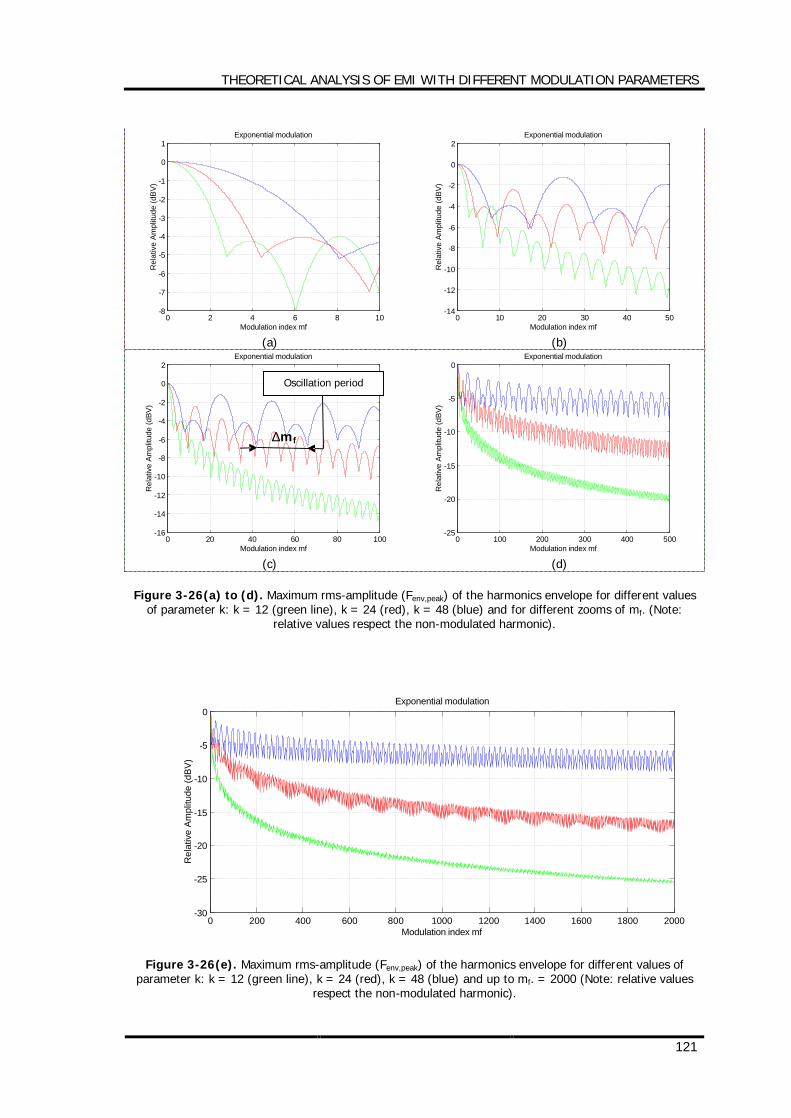
THEORETICAL ANALYSIS OF EMI WITH DIFFERENT MODULATION PARAMETERS
121
0 2 4 6 8 10-8
-7
-6
-5
-4
-3
-2
-1
0
1
Modulation index mf
Rel
ativ
e Am
plitu
de (d
BV)
Exponential modulation
(a)
0 10 20 30 40 50-14
-12
-10
-8
-6
-4
-2
0
2
Modulation index mf
Rel
ativ
e Am
plitu
de (d
BV)
Exponential modulation
(b)
0 20 40 60 80 100-16
-14
-12
-10
-8
-6
-4
-2
0
2
Modulation index mf
Rel
ativ
e Am
plitu
de (d
BV)
Exponential modulation
(c)
0 100 200 300 400 500-25
-20
-15
-10
-5
0
Modulation index mf
Rel
ativ
e Am
plitu
de (d
BV)
Exponential modulation
(d)
Figure 3-26(a) to (d). Maximum rms-amplitude (Fenv,peak) of the harmonics envelope for different values of parameter k: k = 12 (green line), k = 24 (red), k = 48 (blue) and for different zooms of mf. (Note:
relative values respect the non-modulated harmonic).
0 200 400 600 800 1000 1200 1400 1600 1800 2000-30
-25
-20
-15
-10
-5
0
Modulation index mf
Rel
ativ
e A
mpl
itude
(dB
V)
Exponential modulation
Figure 3-26(e). Maximum rms-amplitude (Fenv,peak) of the harmonics envelope for different values of parameter k: k = 12 (green line), k = 24 (red), k = 48 (blue) and up to mf. = 2000 (Note: relative values
respect the non-modulated harmonic).
Oscillation period
∆mf
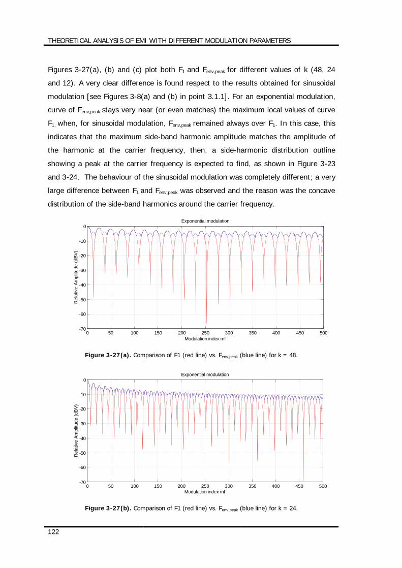
THEORETICAL ANALYSIS OF EMI WITH DIFFERENT MODULATION PARAMETERS
122
Figures 3-27(a), (b) and (c) plot both F1 and Fenv,peak for different values of k (48, 24
and 12). A very clear difference is found respect to the results obtained for sinusoidal
modulation [see Figures 3-8(a) and (b) in point 3.1.1]. For an exponential modulation,
curve of Fenv,peak stays very near (or even matches) the maximum local values of curve
F1, when, for sinusoidal modulation, Fenv,peak remained always over F1. In this case, this
indicates that the maximum side-band harmonic amplitude matches the amplitude of
the harmonic at the carrier frequency, then, a side-harmonic distribution outline
showing a peak at the carrier frequency is expected to find, as shown in Figure 3-23
and 3-24. The behaviour of the sinusoidal modulation was completely different; a very
large difference between F1 and Fenv,peak was observed and the reason was the concave
distribution of the side-band harmonics around the carrier frequency.
0 50 100 150 200 250 300 350 400 450 500-70
-60
-50
-40
-30
-20
-10
0
Modulation index mf
Rel
ativ
e A
mpl
itude
(dB
V)
Exponential modulation
Figure 3-27(a). Comparison of F1 (red line) vs. Fenv,peak (blue line) for k = 48.
0 50 100 150 200 250 300 350 400 450 500-70
-60
-50
-40
-30
-20
-10
0
Modulation index mf
Rel
ativ
e Am
plitu
de (d
BV)
Exponential modulation
Figure 3-27(b). Comparison of F1 (red line) vs. Fenv,peak (blue line) for k = 24.
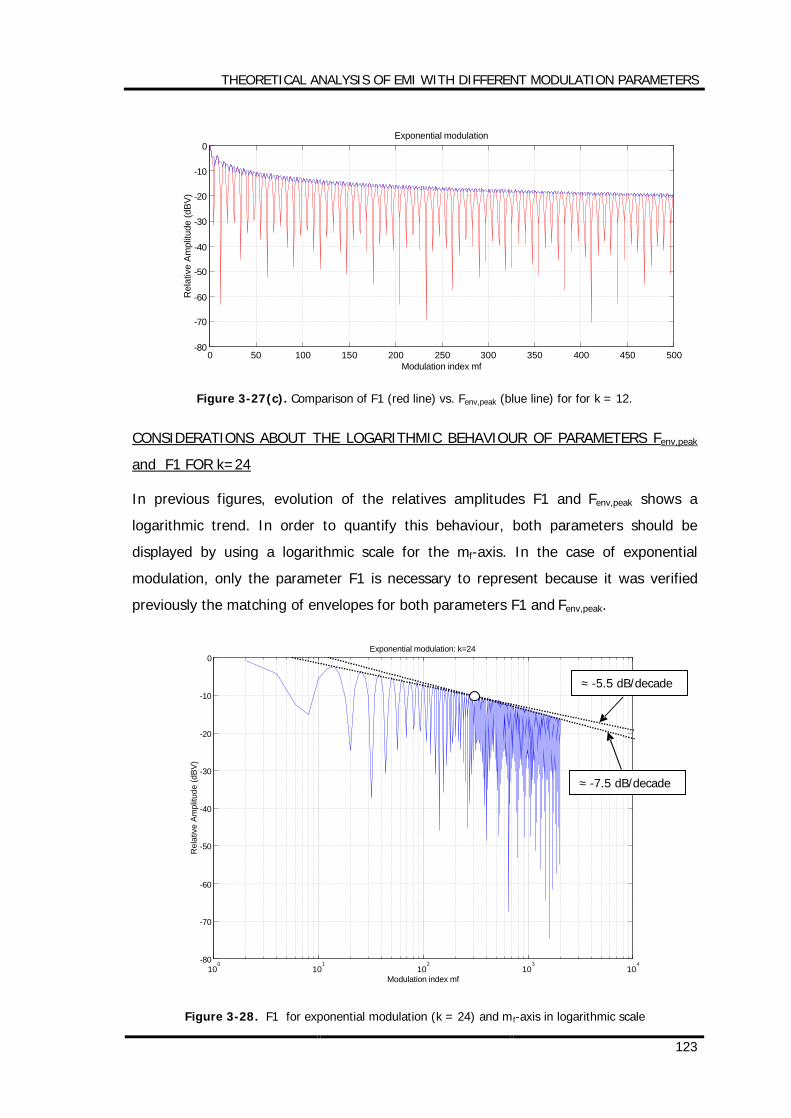
THEORETICAL ANALYSIS OF EMI WITH DIFFERENT MODULATION PARAMETERS
123
0 50 100 150 200 250 300 350 400 450 500-80
-70
-60
-50
-40
-30
-20
-10
0
Modulation index mf
Rel
ativ
e Am
plitu
de (d
BV)
Exponential modulation
Figure 3-27(c). Comparison of F1 (red line) vs. Fenv,peak (blue line) for for k = 12.
CONSIDERATIONS ABOUT THE LOGARITHMIC BEHAVIOUR OF PARAMETERS Fenv,peak
and F1 FOR k=24
In previous figures, evolution of the relatives amplitudes F1 and Fenv,peak shows a
logarithmic trend. In order to quantify this behaviour, both parameters should be
displayed by using a logarithmic scale for the mf-axis. In the case of exponential
modulation, only the parameter F1 is necessary to represent because it was verified
previously the matching of envelopes for both parameters F1 and Fenv,peak.
100
101
102
103
104-80
-70
-60
-50
-40
-30
-20
-10
0
Modulation index mf
Rel
ativ
e A
mpl
itude
(dB
V)
Exponential modulation: k=24
Figure 3-28. F1 for exponential modulation (k = 24) and mf-axis in logarithmic scale
≈ -7.5 dB/decade
≈ -5.5 dB/decade
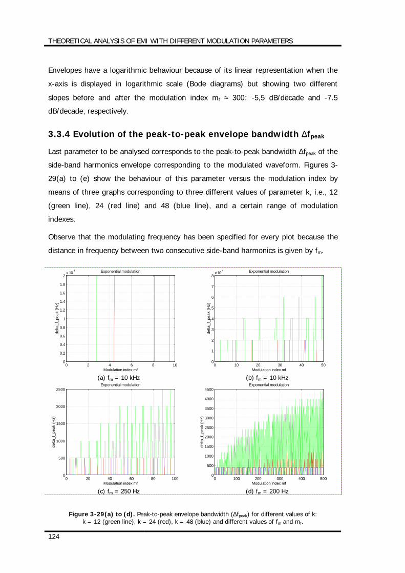
THEORETICAL ANALYSIS OF EMI WITH DIFFERENT MODULATION PARAMETERS
124
Envelopes have a logarithmic behaviour because of its linear representation when the
x-axis is displayed in logarithmic scale (Bode diagrams) but showing two different
slopes before and after the modulation index mf ≈ 300: -5,5 dB/decade and -7.5
dB/decade, respectively.
3.3.4 Evolution of the peak-to-peak envelope bandwidth ∆fpeak
Last parameter to be analysed corresponds to the peak-to-peak bandwidth ∆fpeak of the
side-band harmonics envelope corresponding to the modulated waveform. Figures 3-
29(a) to (e) show the behaviour of this parameter versus the modulation index by
means of three graphs corresponding to three different values of parameter k, i.e., 12
(green line), 24 (red line) and 48 (blue line), and a certain range of modulation
indexes.
Observe that the modulating frequency has been specified for every plot because the
distance in frequency between two consecutive side-band harmonics is given by fm.
0 2 4 6 8 100
0.2
0.4
0.6
0.8
1
1.2
1.4
1.6
1.8
2x 10 4
Modulation index mf
delta
_f_p
eak
(Hz)
Exponential modulation
(a) fm = 10 kHz
0 10 20 30 40 500
1
2
3
4
5
6
7
8x 10 4
Modulation index mf
delta
_f_p
eak
(Hz)
Exponential modulation
(b) fm = 10 kHz
0 20 40 60 80 1000
500
1000
1500
2000
2500
Modulation index mf
delta
_f_p
eak
(Hz)
Exponential modulation
(c) fm = 250 Hz
0 100 200 300 400 5000
500
1000
1500
2000
2500
3000
3500
4000
4500
Modulation index mf
delta
_f_p
eak
(Hz)
Exponential modulation
(d) fm = 200 Hz
Figure 3-29(a) to (d). Peak-to-peak envelope bandwidth (∆fpeak) for different values of k: k = 12 (green line), k = 24 (red), k = 48 (blue) and different values of fm and mf.
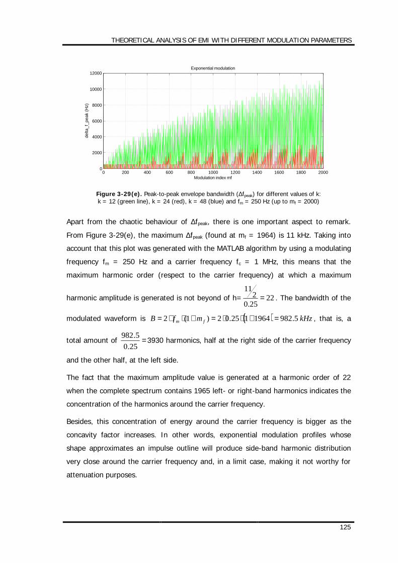
THEORETICAL ANALYSIS OF EMI WITH DIFFERENT MODULATION PARAMETERS
125
0 200 400 600 800 1000 1200 1400 1600 1800 20000
2000
4000
6000
8000
10000
12000
Modulation index mf
delta
_f_p
eak
(Hz)
Exponential modulation
Figure 3-29(e). Peak-to-peak envelope bandwidth (∆fpeak) for different values of k: k = 12 (green line), k = 24 (red), k = 48 (blue) and fm = 250 Hz (up to mf = 2000)
Apart from the chaotic behaviour of ∆fpeak, there is one important aspect to remark.
From Figure 3-29(e), the maximum ∆fpeak (found at mf = 1964) is 11 kHz. Taking into
account that this plot was generated with the MATLAB algorithm by using a modulating
frequency fm = 250 Hz and a carrier frequency fc = 1 MHz, this means that the
maximum harmonic order (respect to the carrier frequency) at which a maximum
harmonic amplitude is generated is not beyond of h= 2225.02
11= . The bandwidth of the
modulated waveform is ( ) kHzmfB fm 5.9821964125.02)1(2 =+⋅⋅=+⋅⋅= , that is, a
total amount of =25.0
5.9823930 harmonics, half at the right side of the carrier frequency
and the other half, at the left side.
The fact that the maximum amplitude value is generated at a harmonic order of 22
when the complete spectrum contains 1965 left- or right-band harmonics indicates the
concentration of the harmonics around the carrier frequency.
Besides, this concentration of energy around the carrier frequency is bigger as the
concavity factor increases. In other words, exponential modulation profiles whose
shape approximates an impulse outline will produce side-band harmonic distribution
very close around the carrier frequency and, in a limit case, making it not worthy for
attenuation purposes.

THEORETICAL ANALYSIS OF EMI WITH DIFFERENT MODULATION PARAMETERS
126
3.4 Comparison of the different modulation profiles
In order to make a useful comparison of the different modulation profiles here
presented, only those profiles whose characteristics seem to be better are to be
selected. In the case of a sinusoidal modulation, there is nothing to choose because no
shape parameters are to be selected. In the triangular modulation case, the shape
parameter s is the one making differences. A value of the parameter s = 0.5 is
preferred because it may be used to cancel the harmonic at the carrier frequency (see
clause 3.2). Respect to the exponential modulation profile, a low concavity factor k =
12 is selected because it produces a very good attenuation of both F1 and Fenv,peak.
Anyway, this comparison is related to a first approximation to the most profitable
modulation profile to be used in power converters. Some ideas will arise from this
analysis, pointing to a concrete specification about requirements for power converters.
0 10 20 30 40 50-100
-80
-60
-40
-20
0
20
Modulation index mf
Rel
ativ
e Am
plitu
de (d
BV)
F1 for different modulation profiles
(a)
0 100 200 300 400 500-120
-100
-80
-60
-40
-20
0
20
Modulation index mf
Rel
ativ
e Am
plitu
de (d
BV)
F1 for different modulation profiles
(b)
Figure 3-30(a) and (b). Relative rms-amplitude (F1) of the carrier harmonic for different modulation profiles: sinusoidal (green), triangular [s = 0.5] (red) and exponential [k = 12] (blue) for two zooms of mf.
0 10 20 30 40 50-18
-16
-14
-12
-10
-8
-6
-4
-2
0
2
Modulation index mf
Rel
ativ
e Am
plitu
de (d
BV)
Fenv,peak for different modulation profiles
(a)
0 100 200 300 400 500-30
-25
-20
-15
-10
-5
0
5
Modulation index mf
Rel
ativ
e Am
plitu
de (d
BV)
Fenv,peak for different modulation profiles
(b)
Figure 3-31(a) and (b). Relative rms-amplitude of Fenv,peak for different modulation profiles: sinusoidal (green), triangular [s = 0.5] (red) and exponential [k = 12] (blue) for two zooms of mf.
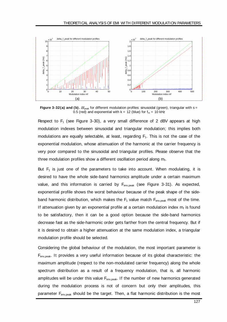
THEORETICAL ANALYSIS OF EMI WITH DIFFERENT MODULATION PARAMETERS
127
0 10 20 30 40 500
1
2
3
4
5
6
7
8
9
10x 10 5
Modulation index mf
delta
_f_p
eak
(Hz)
delta_f_peak for different modulation profiles
(a)
0 100 200 300 400 5000
0.2
0.4
0.6
0.8
1
1.2
1.4
1.6
1.8
2x 10 5
Modulation index mf
delta
_f_p
eak
(Hz)
delta_f_peak for different modulation profiles
(b)
Figure 3-32(a) and (b). ∆fpeak for different modulation profiles: sinusoidal (green), triangular with s = 0.5 (red) and exponential with k = 12 (blue) for fm = 10 kHz
Respect to F1 (see Figure 3-30), a very small difference of 2 dBV appears at high
modulation indexes between sinusoidal and triangular modulation; this implies both
modulations are equally selectable, at least, regarding F1. This is not the case of the
exponential modulation, whose attenuation of the harmonic at the carrier frequency is
very poor compared to the sinusoidal and triangular profiles. Please observe that the
three modulation profiles show a different oscillation period along mf.
But F1 is just one of the parameters to take into account. When modulating, it is
desired to have the whole side-band harmonics amplitude under a certain maximum
value, and this information is carried by Fenv,peak (see Figure 3-31). As expected,
exponential profile shows the worst behaviour because of the peak shape of the side-
band harmonic distribution, which makes the F1 value match Fenv,peak most of the time.
If attenuation given by an exponential profile at a certain modulation index mf is found
to be satisfactory, then it can be a good option because the side-band harmonics
decrease fast as the side-harmonic order gets farther from the central frequency. But if
it is desired to obtain a higher attenuation at the same modulation index, a triangular
modulation profile should be selected.
Considering the global behaviour of the modulation, the most important parameter is
Fenv,peak. It provides a very useful information because of its global characteristic: the
maximum amplitude (respect to the non-modulated carrier frequency) along the whole
spectrum distribution as a result of a frequency modulation, that is, all harmonic
amplitudes will be under this value Fenv,peak. If the number of new harmonics generated
during the modulation process is not of concern but only their amplitudes, this
parameter Fenv,peak should be the target. Then, a flat harmonic distribution is the most
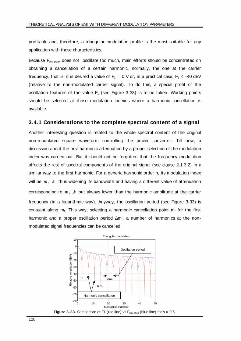
THEORETICAL ANALYSIS OF EMI WITH DIFFERENT MODULATION PARAMETERS
128
profitable and, therefore, a triangular modulation profile is the most suitable for any
application with these characteristics.
Because Fenv,peak does not oscillate too much, main efforts should be concentrated on
obtaining a cancellation of a certain harmonic, normally, the one at the carrier
frequency, that is, it is desired a value of F1 = 0 V or, in a practical case, F1 < -40 dBV
(relative to the non-modulated carrier signal). To do this, a special profit of the
oscillation features of the value F1 (see Figure 3-33) is to be taken. Working points
should be selected at those modulation indexes where a harmonic cancellation is
available.
3.4.1 Considerations to the complete spectral content of a signal
Another interesting question is related to the whole spectral content of the original
non-modulated square waveform controlling the power converter. Till now, a
discussion about the first harmonic attenuation by a proper selection of the modulation
index was carried out. But it should not be forgotten that the frequency modulation
affects the rest of spectral components of the original signal (see clause 2.1.3.2) in a
similar way to the first harmonic. For a generic harmonic order h, its modulation index
will be hm f ⋅ , thus widening its bandwidth and having a different value of attenuation
corresponding to hm f ⋅ but always lower than the harmonic amplitude at the carrier
frequency (in a logarithmic way). Anyway, the oscillation period (see Figure 3-33) is
constant along mf. This way, selecting a harmonic cancellation point mf for the first
harmonic and a proper oscillation period ∆mf, a number of harmonics at the non-
modulated signal frequencies can be cancelled.
0 10 20 30 40 50-80
-70
-60
-50
-40
-30
-20
-10
0
10
Modulation index mf
Rel
ativ
e Am
plitu
de (d
BV)
Triangular modulation
Figure 3-33. Comparison of F1 (red line) vs Fenv,peak (blue line) for s = 0.5.
Harmonic cancellation
Oscillation period
∆mf mf
h⋅mf
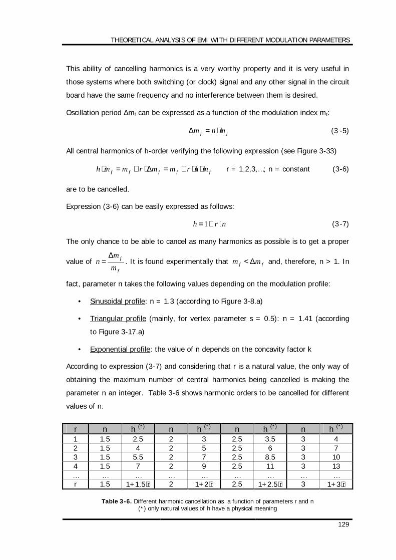
THEORETICAL ANALYSIS OF EMI WITH DIFFERENT MODULATION PARAMETERS
129
This ability of cancelling harmonics is a very worthy property and it is very useful in
those systems where both switching (or clock) signal and any other signal in the circuit
board have the same frequency and no interference between them is desired.
Oscillation period ∆mf can be expressed as a function of the modulation index mf:
ff mnm ⋅=∆ (3 -5)
All central harmonics of h-order verifying the following expression (see Figure 3-33)
fffff mnrmmrmmh ⋅⋅+=∆⋅+=⋅ r = 1,2,3,…; n = constant (3-6)
are to be cancelled.
Expression (3-6) can be easily expressed as follows:
nrh ⋅+=1 (3-7)
The only chance to be able to cancel as many harmonics as possible is to get a proper
value of f
f
mm
n∆
= . It is found experimentally that ff mm ∆< and, therefore, n > 1. In
fact, parameter n takes the following values depending on the modulation profile:
• Sinusoidal profile: n = 1.3 (according to Figure 3-8.a)
• Triangular profile (mainly, for vertex parameter s = 0.5): n = 1.41 (according
to Figure 3-17.a)
• Exponential profile: the value of n depends on the concavity factor k
According to expression (3-7) and considering that r is a natural value, the only way of
obtaining the maximum number of central harmonics being cancelled is making the
parameter n an integer. Table 3-6 shows harmonic orders to be cancelled for different
values of n.
r n h (*) n h (*) n h (*) n h (*) 1 1.5 2.5 2 3 2.5 3.5 3 4 2 1.5 4 2 5 2.5 6 3 7 3 1.5 5.5 2 7 2.5 8.5 3 10 4 1.5 7 2 9 2.5 11 3 13 … … … … … … … … … r 1.5 1+1.5⋅r 2 1+2⋅r 2.5 1+2.5⋅r 3 1+3⋅r
Table 3-6. Different harmonic cancellation as a function of parameters r and n (*) only natural values of h have a physical meaning
THEORETICAL ANALYSIS OF EMI WITH DIFFERENT MODULATION PARAMETERS
130
According to Table 3-6, the most profitable option is related to the parameter n to be
equal to 2. This value makes possible the cancellation of every odd harmonic amplitude
of the non-modulated signal at its central frequency (please remember that a side-
band harmonics window is also appearing, but the central frequency corresponding to
the odd harmonic order of the non-modulated signal is to be cancelled).
As explained before, exponential profile may be used to tune the oscillation period just
selecting a proper concavity factor k and this key point, together with the results of
Table 3-6, points to the direct application of SSCG in order to avoid disturbing another
significant signal (for instance, a CAN bus telegram inside a car) at the same frequency
as the switching power converter. This is developed in more detail further in clause
4.5.
To sum up, another successful key is to select a modulation index mf and an oscillation
period cancelling as many main harmonics as possible. Oscillation period is only
tuneable for an exponential modulation profile, through its concavity factor k. For
sinusoidal and triangular modulations, no way of tuning is possible. Consequently, the
following aspects are to be considered:
− Tuning of the oscillation period is possible for exponential profiles, thus allowing
the selection of a certain modulation index and, afterwards, tune the related profile
through the concavity factor k.
− If no exponential profile is to be used, no tune of the oscillation period is possible.
Another extra consideration to be careful is the one related to the spectrum overlap
corresponding to contiguous main harmonics (see clause 2.2.2). And, of course,
the problems associated to the use of regulatory RBW's in spectrum analysers (see
Annexes 1 and 2).
3.4.2 Considerations to the spectra distribution shape
From the previous analysis and theoretical calculations of the harmonic spectra
resulting from a frequency modulation process, some important conclusions can be
hereby presented (see Figure 3-34). The first one is related to the triangular
modulation profile. These profiles are the unique modulating waveforms which produce
a complete flat spectrum distribution shape, independently on the sawtooth parameter
s (see related considerations in clause 3.2) as shown in Figures 3-34(c) and (d).
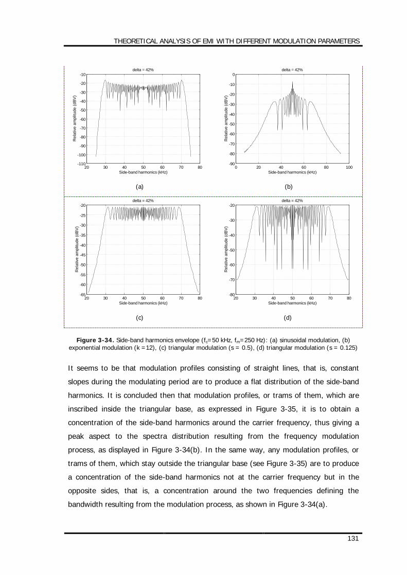
THEORETICAL ANALYSIS OF EMI WITH DIFFERENT MODULATION PARAMETERS
131
20 30 40 50 60 70 80-110
-100
-90
-80
-70
-60
-50
-40
-30
-20
-10delta = 42%
Side-band harmonics (kHz)
Rel
ativ
e am
plitu
de (d
BV)
(a)
0 20 40 60 80 100-90
-80
-70
-60
-50
-40
-30
-20
-10
0
Side-band harmonics (kHz)
Rel
ativ
e am
plitu
de (d
BV)
delta = 42%
(b)
20 30 40 50 60 70 80-65
-60
-55
-50
-45
-40
-35
-30
-25
-20
Side-band harmonics (kHz)
Rel
ativ
e am
plitu
de (d
BV)
delta = 42%
(c)
20 30 40 50 60 70 80-80
-70
-60
-50
-40
-30
-20
Side-band harmonics (kHz)
Rel
ativ
e am
plitu
de (d
BV)
delta = 42%
(d)
Figure 3-34. Side-band harmonics envelope (fc=50 kHz, fm=250 Hz): (a) sinusoidal modulation, (b) exponential modulation (k =12), (c) triangular modulation (s = 0.5), (d) triangular modulation (s = 0.125)
It seems to be that modulation profiles consisting of straight lines, that is, constant
slopes during the modulating period are to produce a flat distribution of the side-band
harmonics. It is concluded then that modulation profiles, or trams of them, which are
inscribed inside the triangular base, as expressed in Figure 3-35, it is to obtain a
concentration of the side-band harmonics around the carrier frequency, thus giving a
peak aspect to the spectra distribution resulting from the frequency modulation
process, as displayed in Figure 3-34(b). In the same way, any modulation profiles, or
trams of them, which stay outside the triangular base (see Figure 3-35) are to produce
a concentration of the side-band harmonics not at the carrier frequency but in the
opposite sides, that is, a concentration around the two frequencies defining the
bandwidth resulting from the modulation process, as shown in Figure 3-34(a).
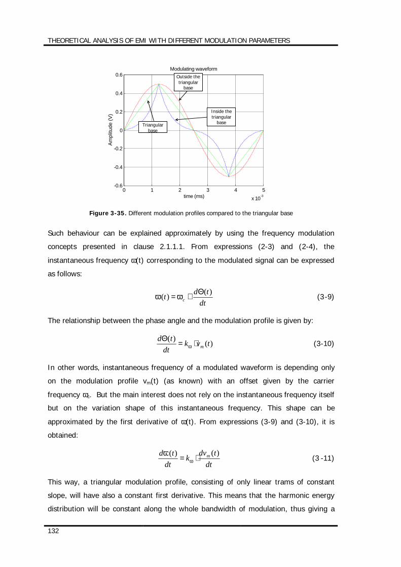
THEORETICAL ANALYSIS OF EMI WITH DIFFERENT MODULATION PARAMETERS
132
0 1 2 3 4 5x 10⁻³
-0.6
-0.4
-0.2
0
0.2
0.4
0.6Modulating waveform
time (ms)
Ampl
itude
(V)
Figure 3-35. Different modulation profiles compared to the triangular base
Such behaviour can be explained approximately by using the frequency modulation
concepts presented in clause 2.1.1.1. From expressions (2-3) and (2-4), the
instantaneous frequency ω(t) corresponding to the modulated signal can be expressed
as follows:
dttdt c)()( Θ
+= ωω (3-9)
The relationship between the phase angle and the modulation profile is given by:
)()( tvkdt
tdm⋅=
Θω (3-10)
In other words, instantaneous frequency of a modulated waveform is depending only
on the modulation profile vm(t) (as known) with an offset given by the carrier
frequency ωc. But the main interest does not rely on the instantaneous frequency itself
but on the variation shape of this instantaneous frequency. This shape can be
approximated by the first derivative of ω(t). From expressions (3-9) and (3-10), it is
obtained:
dttdvk
dttd m )()(
⋅= ωω
(3 -11)
This way, a triangular modulation profile, consisting of only linear trams of constant
slope, will have also a constant first derivative. This means that the harmonic energy
distribution will be constant along the whole bandwidth of modulation, thus giving a
Inside the triangular
base
Outside the triangular
base
Triangular base
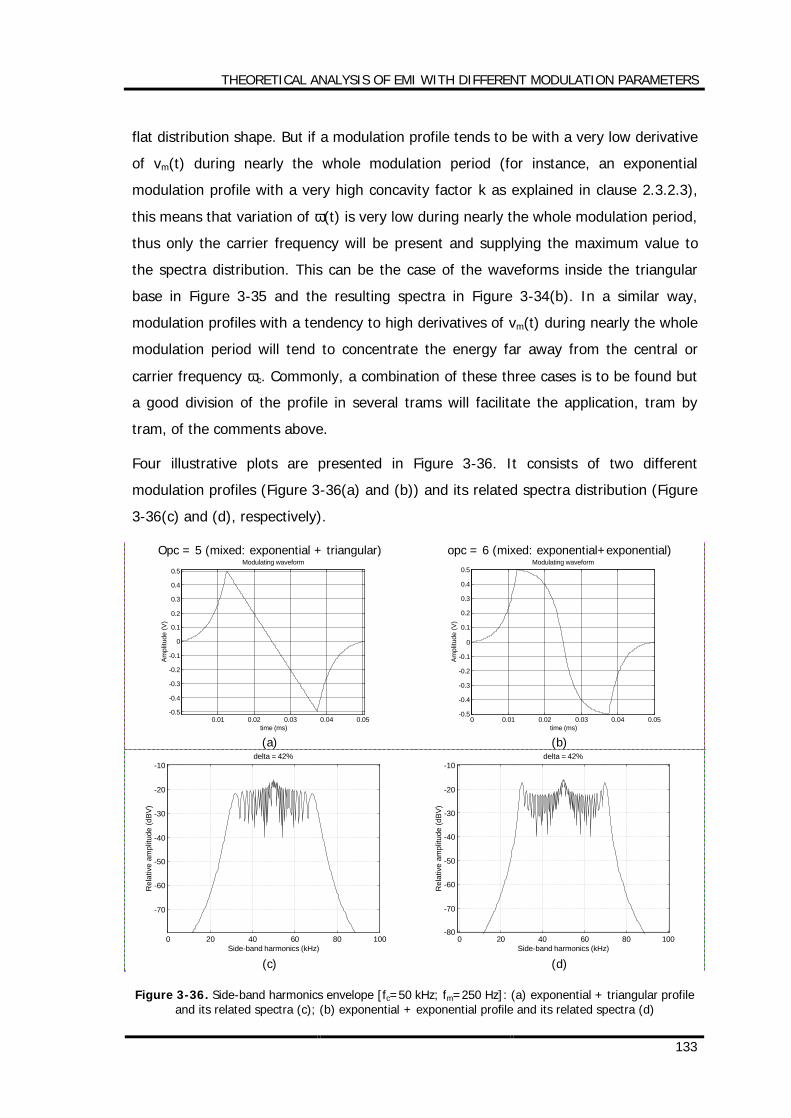
THEORETICAL ANALYSIS OF EMI WITH DIFFERENT MODULATION PARAMETERS
133
flat distribution shape. But if a modulation profile tends to be with a very low derivative
of vm(t) during nearly the whole modulation period (for instance, an exponential
modulation profile with a very high concavity factor k as explained in clause 2.3.2.3),
this means that variation of ω(t) is very low during nearly the whole modulation period,
thus only the carrier frequency will be present and supplying the maximum value to
the spectra distribution. This can be the case of the waveforms inside the triangular
base in Figure 3-35 and the resulting spectra in Figure 3-34(b). In a similar way,
modulation profiles with a tendency to high derivatives of vm(t) during nearly the whole
modulation period will tend to concentrate the energy far away from the central or
carrier frequency ωc. Commonly, a combination of these three cases is to be found but
a good division of the profile in several trams will facilitate the application, tram by
tram, of the comments above.
Four illustrative plots are presented in Figure 3-36. It consists of two different
modulation profiles (Figure 3-36(a) and (b)) and its related spectra distribution (Figure
3-36(c) and (d), respectively).
Opc = 5 (mixed: exponential + triangular)
0.01 0.02 0.03 0.04 0.05-0.5
-0.4
-0.3
-0.2
-0.1
0
0.1
0.2
0.3
0.4
0.5
time (ms)
Ampl
itude
(V)
Modulating waveform
(a)
opc = 6 (mixed: exponential+exponential)
0 0.01 0.02 0.03 0.04 0.05-0.5
-0.4
-0.3
-0.2
-0.1
0
0.1
0.2
0.3
0.4
0.5
time (ms)
Ampl
itude
(V)
Modulating waveform
(b)
0 20 40 60 80 100
-70
-60
-50
-40
-30
-20
-10
Side-band harmonics (kHz)
Rel
ativ
e am
plitu
de (d
BV)
delta = 42%
(c)
0 20 40 60 80 100-80
-70
-60
-50
-40
-30
-20
-10
Side-band harmonics (kHz)
Rel
ativ
e am
plitu
de (d
BV)
delta = 42%
(d)
Figure 3-36. Side-band harmonics envelope [fc=50 kHz; fm=250 Hz]: (a) exponential + triangular profile and its related spectra (c); (b) exponential + exponential profile and its related spectra (d)
THEORETICAL ANALYSIS OF EMI WITH DIFFERENT MODULATION PARAMETERS
134
For the case (a)-(c), one half of the modulation period matches exactly a triangular
signal while the other half stays inside this theoretical triangular profile. The triangular
half tends to get a flat spectra distribution while the exponential half tries
concentrating this distribution around the carrier or central frequency. This way, the
outline of the resulting spectra distribution is neither flat (as expected for a triangular
profile) nor a peak outline (as expected for an exponential profile). The case (b)-(d) is
even more significant. Two exponential curves are combined in such a way that the
resulting profile is half a period outside the theoretical base waveform and half a
period inside this triangular base. The half tram outside the triangular limit will tend to
concentrate side-band harmonics around the two frequencies defining the bandwidth
generated during the frequency modulation process. In a similar way, the half tram
inside the triangular limit tends to concentrate the side-band harmonics around the
carrier frequency. Therefore, a final harmonic distribution shape consisting of three
peaks (the central and the extreme ones) is to be obtained.
This can be an interesting line of investigation in order to study how different
combinations of mathematical profiles should be combined in order to obtain a specific
benefit when using SSCG.
3.5 Proposal of control for a real power converter
Pulse-Width Modulation (PWM) is one of the methods to control the output voltage of a
power converter. This method employs switching at a constant frequency, adjusting
the ton duration of the switch to control the average output voltage.
In the PWM switching at a constant switching frequency, the switch control signal,
which controls the state (on and off) of the switch, is generated by comparing a signal
level control voltage vcontrol with a repetitive waveform as shown in Figures 3-37(a) and
(b). From the general theory of control, the voltage vcontrol is usually obtained by
amplifying the error signal, that is, the difference between the actual voltage control
and its desired value. The comparison between the repetitive sawtooth waveform
(which indeed establishes the switching frequency) and the control voltage vcontrol
produces a square waveform whose duty-cycle is determined by the ratio
st
control
s
on
Vv
TtD == because, when the amplified error signal is greater than the sawtooh
waveform, the switch control signal becomes high, causing the transistor to turn on
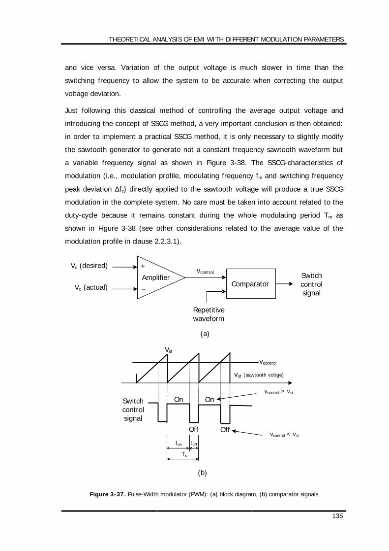
THEORETICAL ANALYSIS OF EMI WITH DIFFERENT MODULATION PARAMETERS
135
and vice versa. Variation of the output voltage is much slower in time than the
switching frequency to allow the system to be accurate when correcting the output
voltage deviation.
Just following this classical method of controlling the average output voltage and
introducing the concept of SSCG method, a very important conclusion is then obtained:
in order to implement a practical SSCG method, it is only necessary to slightly modify
the sawtooth generator to generate not a constant frequency sawtooth waveform but
a variable frequency signal as shown in Figure 3-38. The SSCG-characteristics of
modulation (i.e., modulation profile, modulating frequency fm and switching frequency
peak deviation ∆fc) directly applied to the sawtooth voltage will produce a true SSCG
modulation in the complete system. No care must be taken into account related to the
duty-cycle because it remains constant during the whole modulating period Tm as
shown in Figure 3-38 (see other considerations related to the average value of the
modulation profile in clause 2.2.3.1).
Figure 3-37. Pulse-Width modulator (PWM): (a) block diagram, (b) comparator signals
Comparator
Vo (desired)
Vo (actual)
Amplifier
+
_
vcontrol
Repetitive waveform
Switch control signal
(a)
vcontrol
vst (sawtooth voltge)
Vst
Switch control signal
On On
Off Off
ton toff
Ts
vcontrol > vst
vcontrol < vst
(b)
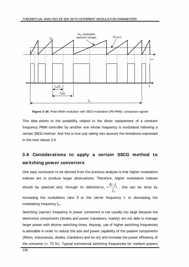
THEORETICAL ANALYSIS OF EMI WITH DIFFERENT MODULATION PARAMETERS
136
Figure 3-38. Pulse Width modulator with SSCG modulation (FM-PWM): comparator signals
This idea points to the possibility related to the direct replacement of a constant
frequency PWM controller by another one whose frequency is modulated following a
certain SSCG method. And this is true just taking into account the limitations expressed
in the next clause 3.6.
3.6 Considerations to apply a certain SSCG method to
switching power converters
One easy conclusion to be derived from the previous analysis is that higher modulation
indexes are to produce larger attenuations. Therefore, higher modulation indexes
should be selected and, through its definitionm
cf f
fm ⋅=
δ, this can be done by
increasing the modulation ratio δ or the carrier frequency fc or decreasing the
modulating frequency fm.
Switching (carrier) frequency in power converters is not usually too large because the
electronics components (diodes and power transistors, mainly) are not able to manage
larger power with shorter switching times. Anyway, use of higher switching frequencies
is advisable in order to reduce the size and power capability of the passive components
(filters, inductances, diodes, transistors and so on) and increase the power efficiency of
the converter (> 70 %). Typical commercial switching frequencies for medium powers
ton(t)
Ts(t)
Tm
t
Vst vcontrol
vst (modulated sawtooth voltage)
THEORETICAL ANALYSIS OF EMI WITH DIFFERENT MODULATION PARAMETERS
137
are about 200 kHz or less. For instance, National Semiconductor is offering a SIMPLE
SWITCHER Power Converter (LM2957) at a fixed switching frequency of 150 kHz
managing a maximum output power of 2.5 W (5V, 0.5A) in a step-down topology. The
maximum switching frequency of National Semiconductor's switching regulators is
limited to 300 kHz (for a maximum output current of 200 mA). Switching frequencies
of 1 MHz are also available for low levels of power. Experimental higher frequency
power converters are also under study. A 50MHz to 100MHz dc-dc power converter
using Gallium Arsenide power switches has been studied. GaAs Schottky rectifiers with
high breakdown voltage and very small Ron⋅Con switching quality factor have been
fabricated. A 10V to 5V (or 8V) prototype with an output power of 2.6 Watts and a
power efficiency of 77% has been reported [Gaye, M. and Ajram, S. and Maynadier, P.
and Salmer, G. (2000), "An ultra-high switching frequency step-down DC-DC converter
based on Gallium Arsenide devices". Proceedings Gallium Arsenide applications
symposium. GAAS 2000, Paris.]
If limitations in switching frequencies are found in order to increase the modulation
index, another possibility consists of decreasing the modulating frequency as many as
possible. Depending on the switching frequency, lower modulating frequencies fm can
result in a negligible normative benefit due to the regulatory Resolution Bandwidth to
be adjusted on the compliant Spectrum Analyzer (see Annexes 1 and 2) as verified
experimentally in clause 4.2 in more detail.
Taking into account the limitations related to the switching frequency fc and the
modulating frequency fm, the only chance to increase the modulation index mf comes
from increasing the modulation ratio δ as much as possible. As explained in clause
2.2.3.4, carrier frequency peak deviation cc ff ⋅=∆ δ is limited by power converter's
filter considerations.
These three parameters and their related limitations are to be studied in more detail in
clauses 4.2 and 4.3.
3.7 Summary
In this chapter, a wide analysis regarding the theoretical behaviour of the modulation
profiles was carried out, providing simultaneously a quantification of the modulation
process according to several significant measure parameters: central harmonic

THEORETICAL ANALYSIS OF EMI WITH DIFFERENT MODULATION PARAMETERS
138
amplitude F1, maximum envelope amplitude Fenv,peak and peak-to-peak envelope
bandwidth ∆fpeak. The same procedure of analysis was applied to the three profiles of
interest: sinusoidal, triangular and exponential and the results are summarized in the
following points:
1. Results expected from the analytical expressions of sinusoidal modulation are
exactly reproduced by the computational algorithms, validating again the MATLAB
algorithm.
2. Side-band harmonics resulting from modulation show a different aspect or outline
depending on the profile. For a sinusoidal modulation, side-band harmonics tend to
concentrate themselves around the two peaks defining the side-band harmonics
bandwidth as the modulation index mf gets higher, which results in a shape of the
modulation spectrum envelope showing two peaks at both ends of the bandwidth
while the envelope gets a larger concavity between these two peaks. In the case of
a triangular modulation profile, envelope of the side-band harmonics corresponds
to a nearly flat, straight horizontal line (with harmonic amplitudes concentrated in a
narrow range of variation for vertex index s ≠ 0.5) , very opposite to the sinusoidal
modulation behaviour, characterised by a concavity between two extreme peaks
and to the case of an exponential modulation profile, where side-band harmonics
resulting from the modulation process tend to concentrate around the carrier
frequency, decreasing in amplitude as the side-band harmonic order separates
itself from the carrier frequency.
3. As just said, a triangular modulation produces a flat side-band harmonics spectrum.
Considering a triangular profile as the reference base, profiles plotted outside the
triangular profile limits (e.g., sinusoidal) seems to concentrate harmonics around
the two peaks defining the bandwidth; in the same way, profiles plotted inside the
reference triangular profile (e.g., exponential) concentrate harmonics around the
carrier frequency. A combination of these three cases in a generic modulation
profile allows the designer to generate whichever shape of the side-band
harmonics spectrum.
4. For every modulation profile, amplitude reduction of the side-band harmonics
resulting from the modulation process only depends on the modulation index mf.
5. Regarding the evolution of the central harmonic amplitude F1, the following
considerations for the three profiles under study are of interest:
THEORETICAL ANALYSIS OF EMI WITH DIFFERENT MODULATION PARAMETERS
139
− Representing the harmonic amplitude F1 as a function of mf, it is obtained an
attenuation plot whose envelope results in a logarithmical curve. This way, the
higher the modulation index, the larger the attenuation; however, this
conclusion is only valid considering the envelope. For modulation indexes mf <
200, attenuation increases very fast due to its logarithmical behaviour.
Comparing the three profiles under study, a very small difference of 2 dBV
appears at high modulation indexes between sinusoidal and triangular
modulation; this is not the case of the exponential modulation, whose
attenuation is very poor compared to the two previous profiles.
− Attenuation plots of F1 show oscillations at a constant period of 1.3 (in units of
mf) for sinusoidal modulation, 1.41 for triangular modulation and a value
depending on the concavity factor k for exponential modulation. At every
oscillation along mf -axis, harmonic amplitudes reach a minimum value with
attenuation values higher than 40 dB, that is, it can be said that this harmonic
is cancelled at this particular mf. This way, a special profit can be taken just
tuning the system to a concrete modulation index in order, for instance, to
eliminate the harmonic at the carrier frequency. In the case of exponential
modulation profile, it is possible to let the modulation index fix and tune the
concavity factor k in order to cancel a particular harmonic. In the case of
triangular modulation, no cancellation is possible for vertex index s ≠ 0.5.
6. Regarding the evolution of the maximum envelope amplitude Fenv,peak, consider the
following comments for the three profiles under study:
− Representing the central maximum envelope amplitude Fenv,peak as a function
of mf, it is obtained an attenuation plot whose envelope results in a
logarithmical curve. Again, the higher the modulation index, the larger the
attenuation, only valid considering the envelope of Fenv,peak. For modulation
indexes of mf < 200, attenuation increases very fast due to its logarithmical
behaviour. Comparing the three profiles, exponential profile shows the worst
behaviour because of the peak shape of the side-band harmonic distribution,
which makes the F1 value matches Fenv,peak most of the time; however,
sinusoidal and, in a much higher quantity, triangular modulations give very
good values of attenuation at any side-band harmonic order.
THEORETICAL ANALYSIS OF EMI WITH DIFFERENT MODULATION PARAMETERS
140
− Attenuation plots of Fenv,peak show oscillations much smaller than those
corresponding to F1; because of that, main efforts should be concentrated on
obtaining a cancellation of a certain harmonic, normally, the one at the carrier
frequency.
7. Related to the evolution of the peak-to-peak envelope bandwidth ∆fpeak, further
comments are of interest:
− For sinusoidal modulation, envelope of ∆fpeak shows a linear trend respect to
mf, that is, higher modulation indexes mf are to produce wider bandwidths in
a linear ratio. Zooming the plot of ∆fpeak, it is observed that this parameter
increases in steps of a constant value equal to 2⋅fm.
− For triangular modulation, maximum values of ∆fpeak show a linear trend
respect to mf . Under this theoretical straight line, a chaotic behaviour is
shown, which is strongly related to the flat shape of the side-band harmonic
spectra distribution. However, both sinusoidal and triangular modulations
(with vertex index s = 0.5) show approximately the same straight line slope (≈
2⋅fm); for vertex indexes s different of 0.5, this slope is smaller in triangular
modulation.
− For exponential modulation, opposite to the sinusoidal and triangular profiles,
no linear trend is detected, just a chaotic behaviour of ∆fpeak. Moreover, the
maximum bandwidth ∆fpeak is much smaller than for sinusoidal and triangular
cases. This indicates the concentration of harmonics around the carrier
frequency, which is also bigger as the concavity factor k increases.
8. For every modulation index, it is commonly worthy to work with higher modulation
indexes and, through its definition m
cf f
fm ⋅=
δ, this can be done by increasing the
modulation ratio δ or the carrier frequency fc or decreasing the modulating
frequency fm.
From the comparison of these three different modulation profiles and considering the
global behaviour of the modulation, the most important parameter is Fenv,peak. It
provides a very useful information because of its global characteristic: the maximum
amplitude (respect to the non-modulated carrier frequency) along the whole spectrum
distribution as a result of a frequency modulation, that is, all harmonic amplitudes will
THEORETICAL ANALYSIS OF EMI WITH DIFFERENT MODULATION PARAMETERS
141
be under this value Fenv,peak. If the number of new harmonics generated during the
modulation process is not of concern but only their amplitudes, this parameter Fenv,peak
should be the target. Then, a flat harmonic distribution is the most profitable and,
therefore, a triangular modulation profile is the most suitable for any application with
these characteristics. Exponential profile shows the worst behaviour because of the
peak shape of the side-band harmonic distribution. If attenuation given by an
exponential profile at a certain modulation index mf is found to be satisfactory, then it
can be a good option because the side-band harmonics decrease fast as the side-
harmonic order gets farther from the central frequency
Because Fenv,peak does not oscillate too much, main efforts should be concentrated on
obtaining a cancellation of a certain harmonic, normally, the one at the carrier
frequency, that is, it is desired a value of F1 = 0 V or, in a practical case, F1 < -40 dBV
(relative to the non-modulated carrier signal). To do this, a special profit of the
oscillation features of the value F1 is to be taken. Working points should be selected at
those modulation indexes where harmonic cancellation is available.
Anyway, modulation profile to be selected is depending on the systems necessities or
exigencies and no generic formula can be given.
Finally, a proposal of control applied to a real power converter was presented,
consisting of simply changing the constant frequency control signal (sawtooth
waveform) for a "modulated" sawtooth control signal. In order to be successful, some
considerations must be taken into account: limitations of switching frequency fc
(electronic components are not able to manage easily larger power with shorter
switching times), limitations of modulating frequency fm (due to wider regulatory RBWs
to be used in the compliant Spectrum Analyzers, in the case of being interested in
regulatory measurements, of course) and limitations of modulation ratio δ (due to the
cut-off frequency of the low-pass filter in the power converter).

C H A P T E R
4
APPLICATION OF SSCG TO EMI EMISSIONS
REDUCTION IN SWITCHING POWER
CONVERTERS

APPLICATION OF SSCG TO EMI EMISSIONS REDUCTION IN POWER CONVERTERS
145
4. APPLICATION OF SSCG TO EMI EMISSIONS
REDUCTION IN SWITCHING POWER CONVERTERS
Although most of the power converters are currently designed to operate by using a
constant switching frequency and a variable duty-cycle, some attempts were made in
order to verify the effect of modulating the switching frequency [RA-1] and how this
modulation affected the power converters EMI emissions. As known, Spread Spectrum
Clock Generation (SSCG) modulates the originally constant switching frequency by
following a certain modulation profile in order to spread the single harmonic energy
into an amount of side-band harmonics having the same energy but smaller
amplitudes. This reduction technique has been used and implemented for high
frequencies (as those related to clock frequencies in communications and
microprocessors systems). This chapter is dedicated to SSCG applied to the reduction
of EMI emissions in Switching Power Converters, focusing on the effectiveness of
frequency modulation in EMI reduction as a function of different switching frequency
ranges and modulation profiles. As exposed previously (chapter 2), theoretical results
are obtained just modulating a sine pure wave following several modulation profiles,
this one representing each one of the harmonics composing the real square PWM-
signal controlling the power converter. A practical test plant was designed in order to
generate a modulated square wave from the modulated sinusoidal signal computed by
the algorithm; a complete description of this test plan is also included.
Experimental results from a real power converter (making part of the test plant) will be
measured. A compliant signal generator will be loaded with the corresponding
modulated waveform and its output directly connected to the modulation controller
system and, then, through a compliant LISN, the spectral components coming from the
power converter finally measured with the spectrum analyzer. Now, some divergences
can arise between theoretical results in chapter 3 and the ones here obtained due to
influences of the real converter. When necessary and in order to evaluate the influence
of the real converter on the expected results, it can be advisable to analyze the
modulated signal introducing it directly into the Spectrum Analyzer, that is, the signal
generator will be loaded with the corresponding modulated waveform and its output
directly connected to the spectrum analyzer (according to Figure 4-1). This way, a very
close (nearly exact) relationship must be found between theoretical results and the
ones here obtained, without the influence of the real converter.
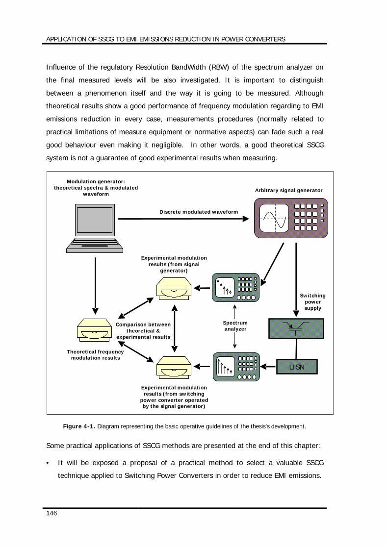
APPLICATION OF SSCG TO EMI EMISSIONS REDUCTION IN POWER CONVERTERS
146
Influence of the regulatory Resolution BandWidth (RBW) of the spectrum analyzer on
the final measured levels will be also investigated. It is important to distinguish
between a phenomenon itself and the way it is going to be measured. Although
theoretical results show a good performance of frequency modulation regarding to EMI
emissions reduction in every case, measurements procedures (normally related to
practical limitations of measure equipment or normative aspects) can fade such a real
good behaviour even making it negligible. In other words, a good theoretical SSCG
system is not a guarantee of good experimental results when measuring.
Figure 4-1. Diagram representing the basic operative guidelines of the thesis's development.
Some practical applications of SSCG methods are presented at the end of this chapter:
• It will be exposed a proposal of a practical method to select a valuable SSCG
technique applied to Switching Power Converters in order to reduce EMI emissions.
Arbitrary signal generator
Theoretical frequency modulation results
Experimental modulation results (from signal
generator)
Experimental modulation results (from switching
power converter operated by the signal generator)
Modulation generator: theoretical spectra & modulated
waveform
LISN
Comparison between theoretical &
experimental results
Spectrum analyzer
Switching power supply
Discrete modulated waveform
APPLICATION OF SSCG TO EMI EMISSIONS REDUCTION IN POWER CONVERTERS
147
• A valuable comparative measurement of conducted EMI within the range of
conducted emissions will be carried out for the three modulation profiles of interest
at different switching frequencies, showing the advantages of using SSCG methods
as a way or EMI reduction.
• Use of SSCG as a method to avoid interferences to a significant signal.
Figure 4-1 summarizes graphically the operation mode for obtaining experimental
results.
GENERIC CONSIDERATIONS (unless otherwise specified):
− Peak amplitude of the sinusoidal carrier signal is 0.5 V.
− Theoretical and experimental results are to be presented as a relative value dBVrel
respect to the non-modulated harmonic amplitude, that is:
carrierrms
harmonicrmsrel V
VV
,
,= è (4 -1)
( ) ( ) ( )carrierrmsharmonicrmsrel VVV ,10,1010 log20log20log20 ⋅−⋅=⋅ (4-2)
dBVrel = dBVharmonic – (-9.0309 dBV) (4-3)
− Modulation profiles are even waveforms with null-offset. Related considerations
were studied in point 2.6.2.4.
− Harmonic components measurements are to be carried out with a compliant
spectrum analyzer (Tektronix 2712) in PEAK mode.
− A Tektronix AWG2021 was selected as the signal generator to be used (refer to
point 4.1.2 for further information).
For the practical considerations about the physical implementation of the test plant
used to measure, please refer to next clause 4.1.3.

APPLICATION OF SSCG TO EMI EMISSIONS REDUCTION IN POWER CONVERTERS
148
4.1 Description of the test plant
Main part of the test plant consists of a switching power conversion system which has
to meet several conditions to be useful:
a) It must be able to work with both a constant and variable frequency PWM. This
way, measurements without modulation are easy to obtain and ready for
comparison with those resulting from a further modulation process. Please note
that the main interest is related to the relative amplitude of spectral contents
before and after the modulation process.
b) A second (and more complicated to meet) condition is related to the ability of this
power conversion system for admitting a modulation of the PWM controlling signal
with no loss of linearity or non-negligible side-effects as explained in clause 4.1.2.
c) No optimization of the power conversion system is necessary to be reached. It is
not an objective of this thesis to develop the best switching power converter in the
world but a conversion system to demonstrate, through an easy verification, the
benefits obtained by the fact of using a SSCG method, i.e., a frequency modulation
following a certain modulation profile. First, a constant frequency PWM signal is to
be applied and the values obtained this way will be measured; second, a frequency
modulation of this controlling PWM will be applied and the new spectra will be
measured. A further comparison between both measurements will reveal whether a
frequency modulation is worthy or not. This is an important aspect which should be
kept in mind during the development of this chapter. In order to test several
switching frequencies, the power conversion system should be able to manage a
relative wide range of frequencies, at least, from 100 kHz to 1 MHz. Of course, the
behaviour of the system will differ from the lowest frequency to the highest one
but this is not of special concern because the main interest is only related to
relative differences under the same environment. Again, power capabilities of this
converter are not of interest; this way, simple power converters are of interest
because they simplify the design of the switching power converter and allow the
use of common electronic components.
d) Finally, in order to meet the criteria imposed by regulatory normative (mainly
CISPR 22 and FCC), measurements will be carried out through a compliant LISN.
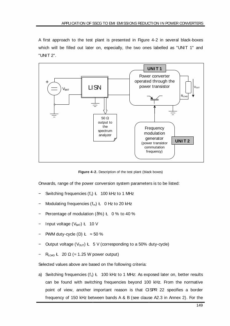
APPLICATION OF SSCG TO EMI EMISSIONS REDUCTION IN POWER CONVERTERS
149
A first approach to the test plant is presented in Figure 4-2 in several black-boxes
which will be filled out later on, especially, the two ones labelled as "UNIT 1" and
"UNIT 2".
Figure 4-2. Description of the test plant (black boxes)
Onwards, range of the power conversion system parameters is to be listed:
− Switching frequencies (fc) è 100 kHz to 1 MHz
− Modulating frequencies (fm) è 0 Hz to 20 kHz
− Percentage of modulation (δ%) è 0 % to 40 %
− Input voltage (VBAT) è 10 V
− PWM duty-cycle (D) è ≈ 50 %
− Output voltage (VOUT) è 5 V (corresponding to a 50% duty-cycle)
− RLOAD è 20 Ω (≈ 1.25 W power output)
Selected values above are based on the following criteria:
a) Switching frequencies (fc) è 100 kHz to 1 MHz: As exposed later on, better results
can be found with switching frequencies beyond 100 kHz. From the normative
point of view, another important reason is that CISPR 22 specifies a border
frequency of 150 kHz between bands A & B (see clause A2.3 in Annex 2). For the
Power converter operated through the
power transistor LISN +
Frequency modulation generator
(power transistor commutation frequency)
50 Ω output to
the spectrum analyzer
RLOAD
VBAT
UNIT 2
VOUT
UNIT 1
APPLICATION OF SSCG TO EMI EMISSIONS REDUCTION IN POWER CONVERTERS
150
band A, a 220Hz-resolution bandwidth must be selected on the spectrum analyzer
to measure. For the band B, this resolution bandwidth increases until 9 kHz. The
resulting compliant measured spectra will be completely different for a power
converter being controlled by a frequency of 145 kHz than the same one but
controlled by a frequency of 155 kHz, at least, for the first harmonic. In the first
case and in a generic situation, harmonics resulting from the modulation process
will be displayed on the spectrum analyzer as individual lines corresponding to true
individual components while, in the second case, each spectral line on the display
can correspond to several true harmonic components, falling inside the wider 9kHz-
resolution bandwidth. In other words, attenuation benefits at 145 kHz or 155 kHz
are true and very similar in practice; however they are different from the normative
point of view, but this is only a conventionalism. This situation will be studied and
the results presented in clause 4.2.
b) Modulating frequencies (fm) è 0 Hz to 20 kHz: Frequency spacing between
harmonics resulting from the modulation process is given directly by fm. Due to the
range of switching frequencies (<1MHz), resolution bandwidths to be configured on
spectrum analyzers are 220 Hz or 9 kHz. The selected range allows to verify the
influence of resolution bandwidths wider and narrower than the modulating
frequency. Besides, the limit of 20 kHz will allow the system to vary the modulation
index mf more widely.
c) Percentage of modulation (δ%) è 0 % to 40 %, depending on the carrier
frequency: For clock systems, the maximum percentage of modulation is commonly
2.5%. For the lower frequency system under study in this thesis, a wider range of
percentages has been assumed in order to investigate the influence of relative high
percentages of modulation in the final harmonic spectra. However, the higher
carrier frequency, the lower percentage of modulation is to be considered; this
way, a maximum percentage of 10% is intended for the highest carrier frequency
of 1 MHz due to limitations of the switching components. A maximum frequency of
1.2 MHz was successfully reached using the test plant, corresponding to δ% =
20% (see Figure 4-10).
d) PWM duty-cycle (D) è ≈ 0.5 (or 50 %): There are two important reasons to select
this value of duty-cycle. The first one, the system hereby developed can generate a
50% duty-cycle square waveform very easily and quite accurately; the second one,
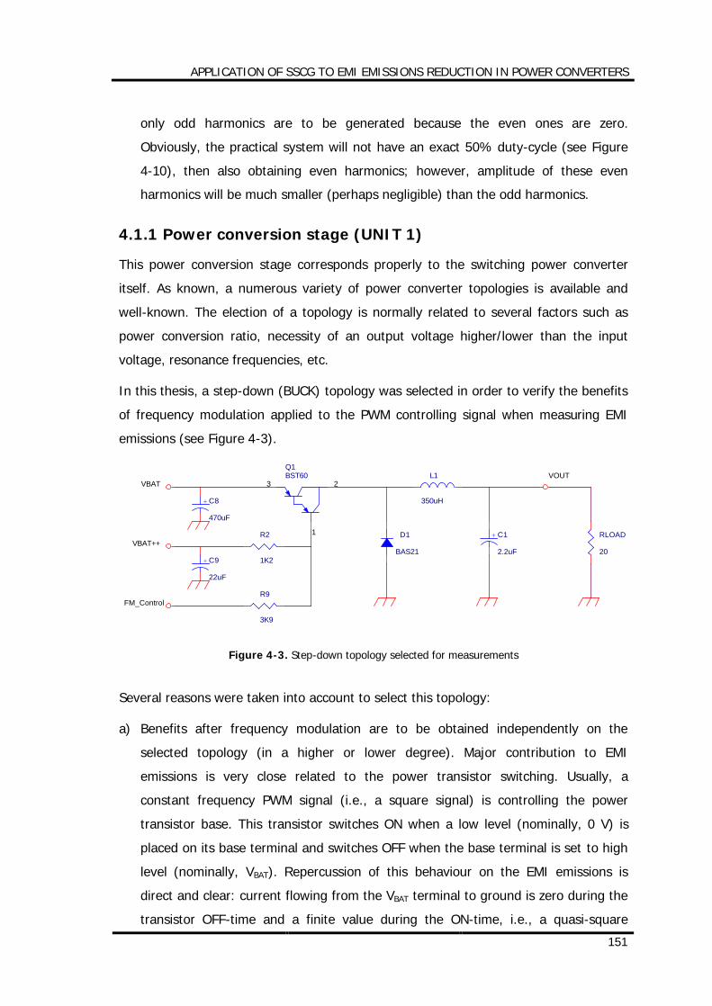
APPLICATION OF SSCG TO EMI EMISSIONS REDUCTION IN POWER CONVERTERS
151
only odd harmonics are to be generated because the even ones are zero.
Obviously, the practical system will not have an exact 50% duty-cycle (see Figure
4-10), then also obtaining even harmonics; however, amplitude of these even
harmonics will be much smaller (perhaps negligible) than the odd harmonics.
4.1.1 Power conversion stage (UNIT 1)
This power conversion stage corresponds properly to the switching power converter
itself. As known, a numerous variety of power converter topologies is available and
well-known. The election of a topology is normally related to several factors such as
power conversion ratio, necessity of an output voltage higher/lower than the input
voltage, resonance frequencies, etc.
In this thesis, a step-down (BUCK) topology was selected in order to verify the benefits
of frequency modulation applied to the PWM controlling signal when measuring EMI
emissions (see Figure 4-3).
R2
1K2
RLOAD
20
L1
350uH
D1
BAS21
VBATVOUT
+ C1
2.2uF
Q1BST60
23
1
R9
3K9
VBAT++
+ C8
470uF
+ C9
22uF
FM_Control
Figure 4-3. Step-down topology selected for measurements
Several reasons were taken into account to select this topology:
a) Benefits after frequency modulation are to be obtained independently on the
selected topology (in a higher or lower degree). Major contribution to EMI
emissions is very close related to the power transistor switching. Usually, a
constant frequency PWM signal (i.e., a square signal) is controlling the power
transistor base. This transistor switches ON when a low level (nominally, 0 V) is
placed on its base terminal and switches OFF when the base terminal is set to high
level (nominally, VBAT). Repercussion of this behaviour on the EMI emissions is
direct and clear: current flowing from the VBAT terminal to ground is zero during the
transistor OFF-time and a finite value during the ON-time, i.e., a quasi-square
APPLICATION OF SSCG TO EMI EMISSIONS REDUCTION IN POWER CONVERTERS
152
current waveform is flowing through the input terminal VBAT, which generates the
corresponding EMI emissions. Shape of the spectral content should be very similar
to that of a square waveform (see clause 2.1.3.1); the absolute magnitude of the
harmonics, however, will depend on several factors like filter capacitors, test plant
layout, parasitic capacitances, length of wires, input and output voltages, load
impedance, PWM- constant switching frequency and duty-ratio, etc. This behaviour
is common to nearly all power converter topologies, thus allowing the selection of
whichever topology if the main purpose is just measuring EMI emissions. Moreover,
instead of having a constant PWM switching frequency, it can be modulated by
using a frequency modulation method. Now, the ON-OFF behaviour of the
transistor will follow the modulated switching frequency and so the currents flowing
through the input terminal VBAT. Then, a different shape of the spectral content
related to the current flowing through the input terminal is to be found and should
be very similar to the spectral content of the modulating signal (i.e., the modulated
PWM switching waveform); again, absolute harmonic magnitude will depend on the
same factor as exposed previously.
b) After the previous consideration a), there is no objection to select a very simple
topology like a step-down converter. This way, main efforts are not concentrated
on the power converter design itself but on the further measurements to be carried
out. As said before, no optimization of the power conversion system is necessary to
be reached because the main interest is related to the relative amplitude of
spectral contents before and after the modulation process.
c) This step-down topology allows an easy design of a system valid for the range of
values expressed before at the beginning of this chapter. As the switching
frequency increases inside the defined variation range, the LC filter (consisting of
L1 and C1) becomes more effective, generating a lower ripple at the output
voltage.
After all these considerations, an exhaustive description of the circuit calculation is
mandatory to be presented. A prestigious reference for the calculation and selection of
all components is [RD-2] and it will be the guideline.
1) Calculation of the LC output filter
This low-pass filter consists of one inductance L1 and one capacitor C1. For
notation reason, these two components will be referred as L and C, respectively,
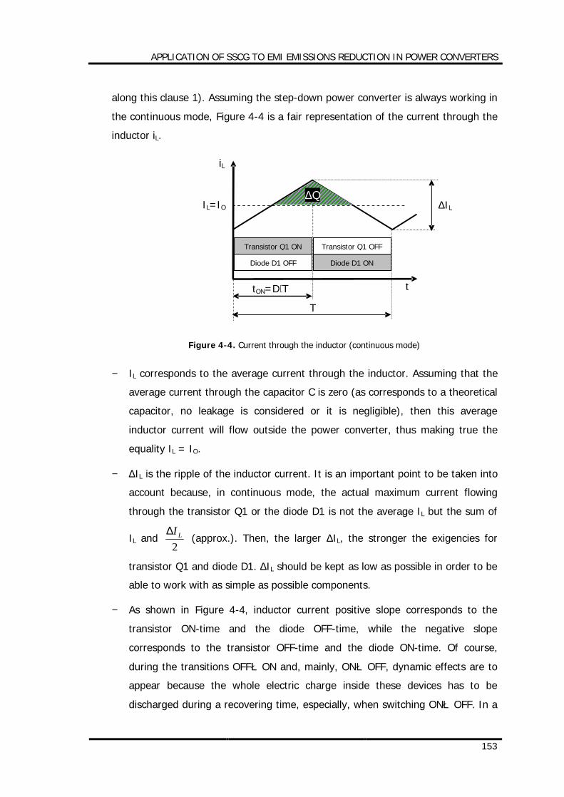
APPLICATION OF SSCG TO EMI EMISSIONS REDUCTION IN POWER CONVERTERS
153
along this clause 1). Assuming the step-down power converter is always working in
the continuous mode, Figure 4-4 is a fair representation of the current through the
inductor iL.
Figure 4-4. Current through the inductor (continuous mode)
− IL corresponds to the average current through the inductor. Assuming that the
average current through the capacitor C is zero (as corresponds to a theoretical
capacitor, no leakage is considered or it is negligible), then this average
inductor current will flow outside the power converter, thus making true the
equality IL = IO.
− ∆IL is the ripple of the inductor current. It is an important point to be taken into
account because, in continuous mode, the actual maximum current flowing
through the transistor Q1 or the diode D1 is not the average IL but the sum of
IL and 2
LI∆ (approx.). Then, the larger ∆IL, the stronger the exigencies for
transistor Q1 and diode D1. ∆IL should be kept as low as possible in order to be
able to work with as simple as possible components.
− As shown in Figure 4-4, inductor current positive slope corresponds to the
transistor ON-time and the diode OFF-time, while the negative slope
corresponds to the transistor OFF-time and the diode ON-time. Of course,
during the transitions OFFèON and, mainly, ONèOFF, dynamic effects are to
appear because the whole electric charge inside these devices has to be
discharged during a recovering time, especially, when switching ONèOFF. In a
iL
IL=IO
tON=D⋅T
T
∆IL
Transistor Q1 ON Transistor Q1 OFF
Diode D1 OFF Diode D1 ON
∆Q
t
APPLICATION OF SSCG TO EMI EMISSIONS REDUCTION IN POWER CONVERTERS
154
first approach, these effects are not taken into account for these preliminary
calculations.
After all these considerations, the calculation of this filter becomes easier now. The
ripple ∆IL is theoretically only depending on the inductor value L, the output voltage
VO, the duty-cycle D and the switching frequency f, as expressed below (4-4):
( )f
DL
VI OL
11 ⋅−⋅=∆ (4-4)
The main consideration to be assumed in order to formulate the expression (4-4) is
that the forward voltage drop through the diode (when switched ON) is zero.
Before being able to apply expression (4-4), an estimation of inductor value L would be
of interest. To do this, relationship between the output voltage VO and its ripple ∆VO is
very useful. This ripple is produced by the charging-discharging process of the real
capacitor C and can be derived by the following steps:
dtdVCi O
c ⋅=
Assuming that the ripple component in iL flows through the capacitor and its average
component flows through the load resistor, the shaded area in Figure 4-4 represents
an additional charge ∆Q. Therefore, the peak-to-peak voltage ripple ∆V0 can be written
as follows:
22211 TI
CCQV L
O ⋅∆
⋅⋅=∆
=∆ (4-5)
From (4-4) and (4-5) (where Tf 1= ):
2
1)1(81
fLCD
VV
O
O ⋅−
⋅=∆
(4-6)
Directly from expression (4-6), the minimum value of inductance Lmin to obtain a
desired maximum ripple at the output takes this aspect:
2min1)1(
8 fCVDVL
O
O ⋅⋅∆
−⋅= (4-7)
A frequency variation range for the switching frequency f from 100 kHz to 1 MHz was
defined. From expression (4-6), the larger switching frequency f, the lower the output
APPLICATION OF SSCG TO EMI EMISSIONS REDUCTION IN POWER CONVERTERS
155
voltage ripple ∆VO. This confirms that calculation of Lmin must be done for the
minimum switching frequency, i.e, for 100 kHz just to limit a maximum output voltage
ripple over the whole range.
Consider the following data in the prototype circuit:
− %)1(01.0=∆
O
O
VV
− C = 2.2 µF è This capacitance value is available in tantalum capacitors which
means, compared to the rest of electrolytic capacitors, a lower ESR and a better
dynamic behaviour. Typical polypropylene capacitor of 100 pF in parallel with C
was not provided in the circuit in order to magnify the EMI results.
− VO = 5 V, f = 100 kHz and D = 0.5 (nominal values)
Substitution of values above into equation (4-7) yields the following result:
HL µ1.284min =
However, the minimum value of inductance only guarantees a minimum ripple of the
output voltage (∆VO). Then, if a limitation of the maximum ripple related to the
inductor current is desired, expression (4-4) becomes now of interest:
( )f
DL
VI OL
11 ⋅−⋅=∆ (4-8)
Substituting values above and the recent value of Lmin, the inductor current ripple to be
obtained is:
mAI L 88=∆
It is a reasonable value, taking into account that the average inductor current is:
mAVR
VIILOAD
OOL 250
205
=Ω
===
However, a larger value of inductance (L>Lmin) is to be selected in order to reduce the
inductor current ripple. A final value of L=L1=350 µH is selected, which yields an
inductor current ripple of:
mAI L 43.71=∆
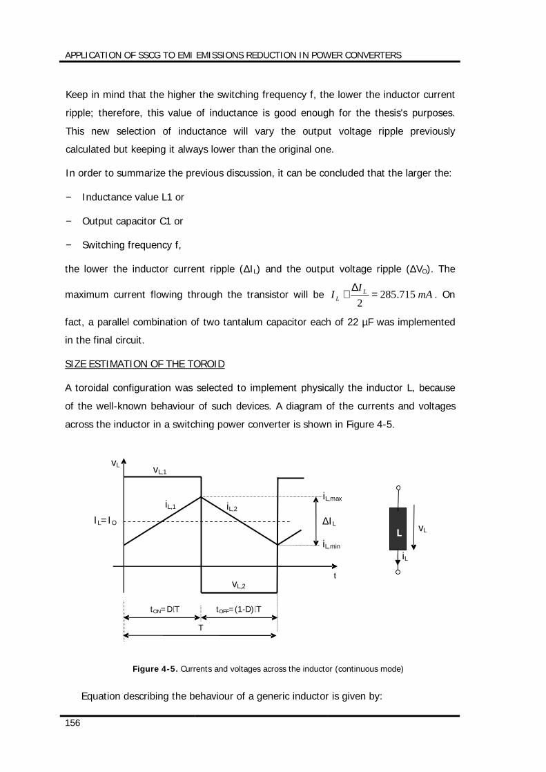
APPLICATION OF SSCG TO EMI EMISSIONS REDUCTION IN POWER CONVERTERS
156
Keep in mind that the higher the switching frequency f, the lower the inductor current
ripple; therefore, this value of inductance is good enough for the thesis's purposes.
This new selection of inductance will vary the output voltage ripple previously
calculated but keeping it always lower than the original one.
In order to summarize the previous discussion, it can be concluded that the larger the:
− Inductance value L1 or
− Output capacitor C1 or
− Switching frequency f,
the lower the inductor current ripple (∆IL) and the output voltage ripple (∆VO). The
maximum current flowing through the transistor will be mAII LL 715.285
2=
∆+ . On
fact, a parallel combination of two tantalum capacitor each of 22 µF was implemented
in the final circuit.
SIZE ESTIMATION OF THE TOROID
A toroidal configuration was selected to implement physically the inductor L, because
of the well-known behaviour of such devices. A diagram of the currents and voltages
across the inductor in a switching power converter is shown in Figure 4-5.
Figure 4-5. Currents and voltages across the inductor (continuous mode)
Equation describing the behaviour of a generic inductor is given by:
IL=IO
tON=D⋅T
T
∆IL
iL,max
iL,min
vL,1
vL,2
L
iL
vL
iL,1 iL,2
t
tOFF=(1-D)⋅T
vL
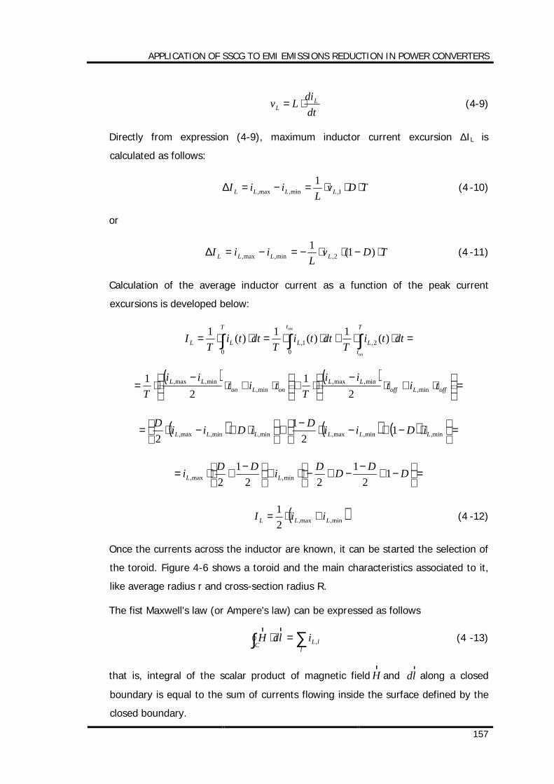
APPLICATION OF SSCG TO EMI EMISSIONS REDUCTION IN POWER CONVERTERS
157
dtdiLv L
L ⋅= (4-9)
Directly from expression (4-9), maximum inductor current excursion ∆IL is
calculated as follows:
TDvL
iiI LLLL ⋅⋅⋅=−=∆ 1,min,max,1
(4 -10)
or
TDvL
iiI LLLL ⋅−⋅⋅−=−=∆ )1(12,min,max, (4 -11)
Calculation of the average inductor current as a function of the peak current
excursions is developed below:
∫∫∫ =⋅⋅+⋅⋅=⋅⋅=T
tL
t
L
T
LL
on
on
dttiT
dttiT
dttiT
I )(1)(1)(12,
01,
0
( ) ( )=
⋅+⋅
−⋅+
⋅+⋅
−⋅= offLoff
LLonLon
LL titii
Ttit
iiT min,
min,max,min,
min,max,
21
21
( ) ( ) ( ) =
⋅−+−⋅
−+
⋅+−⋅= min,min,max,min,min,max, 1
21
2 LLLLLL iDiiDiDiiD
=
−+
−−+−⋅+
−
+⋅= DDDDiDDi LL 12
122
12 min,max,
( )min,max,21
LLL iiI +⋅= (4 -12)
Once the currents across the inductor are known, it can be started the selection of
the toroid. Figure 4-6 shows a toroid and the main characteristics associated to it,
like average radius r and cross-section radius R.
The fist Maxwell's law (or Ampere's law) can be expressed as follows
∑∫ =⋅l
lLCildH ,
rr (4 -13)
that is, integral of the scalar product of magnetic field Hr
and ldr
along a closed
boundary is equal to the sum of currents flowing inside the surface defined by the
closed boundary.

APPLICATION OF SSCG TO EMI EMISSIONS REDUCTION IN POWER CONVERTERS
158
Figure 4-6. Toroid and its related parameters
Assuming that the magnetic field Hr
is constant across the whole toroid section and
perpendicular to it, the middle line of radius r is selected as close boundary.
Expression (4-13) becomes the following one, yielding the module of the magnetic
field H:
LiNrH ⋅=⋅⋅⋅ π2
riNH L
⋅⋅⋅
=π2
(4-14)
where N is the number of wire turns around the toroid.
A non-linear relationship between the magnetic flux density B and the magnetic
field H is characteristic of a ferromagnetic material of which the toroid is made,
relationship expressed normally as the curve in Figure 4-7:
Figure 4-7. Typical histheresis curve of a ferromagnetic material
vL
iL
r
R
iL dl H
H
B
r
c
Bsat
Hsat
APPLICATION OF SSCG TO EMI EMISSIONS REDUCTION IN POWER CONVERTERS
159
It has to be guaranteed that the toroid is never reaching saturation. If so, despite
the growing current across the inductor (therefore, H too), magnetic flux density
keeps a constant value and a null-voltage across the inductor will appear, then
transmitting the supply voltage VBAT directly to the load resistor, causing its
destruction. This is because the inducted voltage ε along the inductor is given by
the variation of magnetic flux φ, as expressed onwards:
dtdN φ
ε ⋅= and ∫ ⋅= sdB rrφ (4 -15)
Ferrite is the selected material for toroid. Ferrite is an ideal core material for
inductors in the frequency range 20 kHz to 3 MHz, due to the combination of low
core cost and low core losses. Different ferrites types are available: F, P, R, K, J
and W. First four types offer the lowest core losses and highest saturation flux
density and are most suitable for high power/high temperature operation. A P-
material core was finally selected for the prototype. Saturation values for P-
material are (approximate values):
− Bsat > 0.5 Tesla at 25 ºC and Bsat > 0.39 Tesla at 100 ºC
− Hsat > 300 A/m.
Selected toroid for the prototype has the following dimensions: r = 12 mm, R = 4
mm (see Figure 4-6). As derived previously, a maximum inductor current of 300
mA is to be flown around the N = 9 turns of wire, then peak-value to be obtained
is calculated directly from expression (4-14):
mA
mmmAturnsH peak 81.35
1223009
=⋅⋅⋅
=π
this peak-value being much lower than the saturation condition Hsat.
To determine the maximum flux density (Bmax) in a core when a symmetrical
square wave excitation is applied, equation (4-16) is applied [RD-6]. If a bias
current is present, the second summand of equation (4-16) must also be taken into
account. The following factors are to be considered:
− applied rms voltage in volts è E ≈ 5 V (voltage across the inductor varies
between +5 V and -5V)
− cross sectional area of the magnetic path in cm2 è Ae≈ π⋅(0.4 cm)2= 0.503 cm2
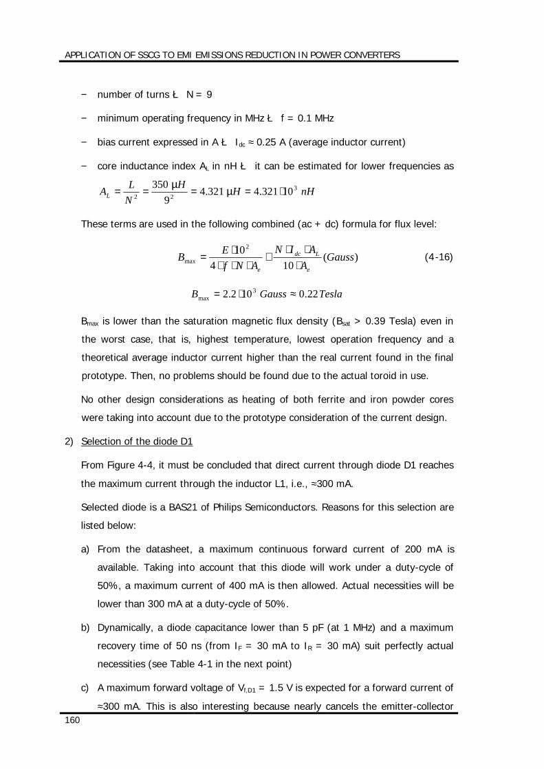
APPLICATION OF SSCG TO EMI EMISSIONS REDUCTION IN POWER CONVERTERS
160
− number of turns è N = 9
− minimum operating frequency in MHz è f = 0.1 MHz
− bias current expressed in A è Idc ≈ 0.25 A (average inductor current)
− core inductance index AL in nH è it can be estimated for lower frequencies as
nHHHNLAL
322 10321.4321.4
9350
⋅==== µµ
These terms are used in the following combined (ac + dc) formula for flux level:
)(104
102
max GaussA
AINANf
EBe
Ldc
e ⋅⋅⋅
+⋅⋅⋅
⋅= (4-16)
TeslaGaussB 22.0102.2 3max ≈⋅=
Bmax is lower than the saturation magnetic flux density (Bsat > 0.39 Tesla) even in
the worst case, that is, highest temperature, lowest operation frequency and a
theoretical average inductor current higher than the real current found in the final
prototype. Then, no problems should be found due to the actual toroid in use.
No other design considerations as heating of both ferrite and iron powder cores
were taking into account due to the prototype consideration of the current design.
2) Selection of the diode D1
From Figure 4-4, it must be concluded that direct current through diode D1 reaches
the maximum current through the inductor L1, i.e., ≈300 mA.
Selected diode is a BAS21 of Philips Semiconductors. Reasons for this selection are
listed below:
a) From the datasheet, a maximum continuous forward current of 200 mA is
available. Taking into account that this diode will work under a duty-cycle of
50%, a maximum current of 400 mA is then allowed. Actual necessities will be
lower than 300 mA at a duty-cycle of 50%.
b) Dynamically, a diode capacitance lower than 5 pF (at 1 MHz) and a maximum
recovery time of 50 ns (from IF = 30 mA to IR = 30 mA) suit perfectly actual
necessities (see Table 4-1 in the next point)
c) A maximum forward voltage of Vf,D1 = 1.5 V is expected for a forward current of
≈300 mA. This is also interesting because nearly cancels the emitter-collector
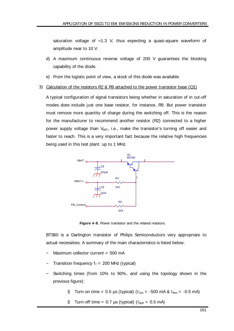
APPLICATION OF SSCG TO EMI EMISSIONS REDUCTION IN POWER CONVERTERS
161
saturation voltage of ≈1.3 V, thus expecting a quasi-square waveform of
amplitude near to 10 V.
d) A maximum continuous reverse voltage of 200 V guarantees the blocking
capability of the diode.
e) From the logistic point of view, a stock of this diode was available.
3) Calculation of the resistors R2 & R9 attached to the power transistor base (Q1)
A typical configuration of signal transistors being whether in saturation of in cut-off
modes does include just one base resistor, for instance, R9. But power transistor
must remove more quantity of charge during the switching off. This is the reason
for the manufacturer to recommend another resistor (R2) connected to a higher
power supply voltage than VBAT, i.e., make the transistor's turning off easier and
faster to reach. This is a very important fact because the relative high frequencies
being used in this test plant: up to 1 MHz.
VBAT
VBAT++
FM_Control
R2
1K2
R9
3K9
+ C8
470uF
+ C9
22uF
Q1BST60
23
1
Figure 4-8. Power transistor and the related resistors.
BTS60 is a Darlington transistor of Philips Semiconductors very appropriate to
actual necessities. A summary of the main characteristics is listed below:
− Maximum collector current = 500 mA
− Transition frequency fT = 200 MHz (typical)
− Switching times (from 10% to 90%, and using the topology shown in the
previous figure):
§ Turn-on time = 0.5 µs (typical) (ICon = -500 mA & IBon = -0.5 mA)
§ Turn-off time = 0.7 µs (typical) (IBoff = 0.5 mA)
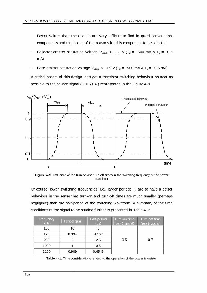
APPLICATION OF SSCG TO EMI EMISSIONS REDUCTION IN POWER CONVERTERS
162
Faster values than these ones are very difficult to find in quasi-conventional
components and this is one of the reasons for this component to be selected.
− Collector-emitter saturation voltage VCEsat < -1.3 V (IC = -500 mA & IB = -0.5
mA)
− Base-emitter saturation voltage VBEsat < -1.9 V (IC = -500 mA & IB = -0.5 mA)
A critical aspect of this design is to get a transistor switching behaviour as near as
possible to the square signal (D ≈ 50 %) represented in the Figure 4-9.
Figure 4-9. Influence of the turn-on and turn-off times in the switching frequency of the power transistor
Of course, lower switching frequencies (i.e., larger periods T) are to have a better
behaviour in the sense that turn-on and turn-off times are much smaller (perhaps
negligible) than the half-period of the switching waveform. A summary of the time
conditions of the signal to be studied further is presented in Table 4-1:
Frequency (kHz) Period (µs) Half-period
(µs) Turn-on time (µs) (typical)
Turn-off time (µs) (typical)
100 10 5
120 8.334 4.167
200 5 2.5
1000 1 0.5
1100 0.909 0.4545
0.5 0.7
Table 4-1. Time considerations related to the operation of the power transistor
vEC/(VBAT+VD1)
0.9 1
0.5
0.1 0
T time
≈toff ≈ton
Theoretical behaviour
Practical behaviour
APPLICATION OF SSCG TO EMI EMISSIONS REDUCTION IN POWER CONVERTERS
163
As expected, turn-off time is a little higher than turn-on time due, mainly, to the
higher recovery time when turning the transistor off. As it can be derived of Figure
4-9, minimum switching period (i.e., maximum switching frequency) is limited by
the turn-on and turn-off times (mainly, by the turn-off time), because the only
possibility for the signal to go from saturation voltage VECsat to VBAT+VD1 is the turn-
off time to be lower or equal (in the worst case) to the half-period of the switching
waveform (considering a 50%-duty cycle) and, in a similar way, the possibility for
the signal to go from saturation voltage VBAT+VD1 to VECsat is the turn-on time to be
lower or equal (in the worst case) to the half-period of the switching waveform
(considering, again, a 50%-duty cycle).
From Table 4-1, problems are only expected at the highest frequency of 1 MHz,
because the typical turn-off time of the power transistor is higher than the related
half period. However, these values are "typical", which means that, after a careful
selection of transistors, a component matching better time behaviour will be found.
The way used to identify a "proper" transistor at 1 MHz consisted of making it
switch at this frequency and measuring the waveform at the collector terminal: if a
"good" quasi-square wave is found at this terminal, having a frequency of 1 MHz
(actually, the same frequency as in the base terminal) and going from VECsat to
VBAT+VD1 and vice versa, it can be said that a proper transistor was found. Pictures
in Figure 4-10 (taken with an oscilloscope Tektronix TDS 510A) are intended to
show this success in the search: the designed power converter is able to manage
frequencies up to ≈1.3 MHz. From the experience, nearly all tested devices
presented lower turn-on and turn-off times than the typical ones, what made this
selection task very easy.
But things can get worse when considering that the original constant frequency of
1 MHz becomes higher due to the frequency modulation. In this sense, the
maximum frequency to be found in this system is given by:
MHzMHzff c 1.1)1.01(1)1( maxmaxmax =+⋅=+⋅= δ
that is, the last case on Table 4-1.
The same considerations above must be taken into account for this maximum
frequency.
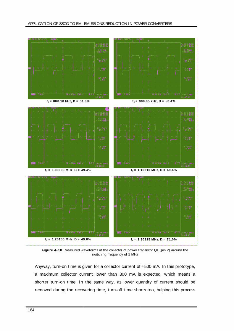
APPLICATION OF SSCG TO EMI EMISSIONS REDUCTION IN POWER CONVERTERS
164
fc = 800.10 kHz, D = 51.0%
fc = 900.05 kHz, D = 50.4%
fc = 1.00000 MHz, D = 49.4%
fc = 1.10310 MHz, D = 49.4%
fc = 1.20150 MHz, D = 49.0%
fc = 1.30315 MHz, D = 71.0%
Figure 4-10. Measured waveforms at the collector of power transistor Q1 (pin 2) around the switching frequency of 1 MHz
Anyway, turn-on time is given for a collector current of ≈500 mA. In this prototype,
a maximum collector current lower than 300 mA is expected, which means a
shorter turn-on time. In the same way, as lower quantity of current should be
removed during the recovering time, turn-off time shorts too, helping this process

APPLICATION OF SSCG TO EMI EMISSIONS REDUCTION IN POWER CONVERTERS
165
by increasing the breaking base current over the 0.5 mA (testing current in
datasheet to estimate turn-off time).
After all these considerations, calculation of these two base resistors is easier to
carry out. Two processes are to be distinguished:
a) Process 1: Power transistor Q1 turns off
Terminal FM_Control is connected to a collector of a signal transistor which controls
the power transistor (Q1) turning-on and -off. When Q1 is turned off, terminal
FM_Control remains unconnected, then actuating just the resistor R2 while, in early
moments, Q1 remains saturated. Under these conditions, the following data are to
be considered:
− VBAT = 10 V
− VBAT++ = VBAT + 2 V = 12 V
− IBQ1off = 3 mA è Current to turn-off the transistor faster.
− VEB1sat = 1.6 V è Emitter-base saturation voltage a few lower than the one
specified in datasheet, due to a lower collector current in the prototype.
VBAT
VBAT++
FM_Control
R2
1K2
R9
3K9
+ C8
470uF
+ C9
22uF
Q1BST60
23
1
Figure 4-11. Schema to analyze the turning-off of the power transistor Q1
Calculation of R2 follows this way:
Ω=+−
= ++ kI
VVVRoffBQ
satEBBATBAT 2.11
12 (4 -17)
Thus, a final value of R2 = 1.2 kΩ is selected.
b) Process 2: Power transistor Q1 turns on
APPLICATION OF SSCG TO EMI EMISSIONS REDUCTION IN POWER CONVERTERS
166
As explained previously, terminal FM_Control is connected to a collector of a signal
transistor Q2 which controls the power transistor (Q1) turning-on and -off. To turn
transistor Q1 on, a low level must be activated at terminal FM_Control, which
implies saturation of control transistor Q2.
Transistor Q2 takes part of a comparator; really, the output of this device consists
of an open-collector transistor. As seen later on, the selected dual comparator was
a LM393 of National Semiconductors. Characteristics of this comparator to be taken
into account at this point are those ones related to the open-collector transistor
and, more, those related to the saturation mode. The following data, obtained from
the LM393 and BST60 datasheets, considered together with the ones shown at
Process 1, are of interest:
− VCE2sat = 0.25 V è Typical collector-emitter saturation voltage for collector
currents lower than 4 mA.
− Comparator is dual-supplied: Vss393+ = +5V & Vss393- = -5V. This is an important
point to take into account because the emitter of the open-collector is
connected to VSS393-, that is, to -5V.
− IBQ1 = 0.3 mA è Q1 base current considering a DC current gain of ≈1000 when
in saturation mode, necessary to supply a collector current of ≈300 mA.
Now, it is time to analyse the circuit already shown before:
VBAT
VBAT++
VSS393-
R2
1K2
R9
3K9
+ C8
470uF
+ C9
22uF
Q1BST60
23
1
Q2
Figure 4-12. Schema to analyze the turning-on of the transistor Q2
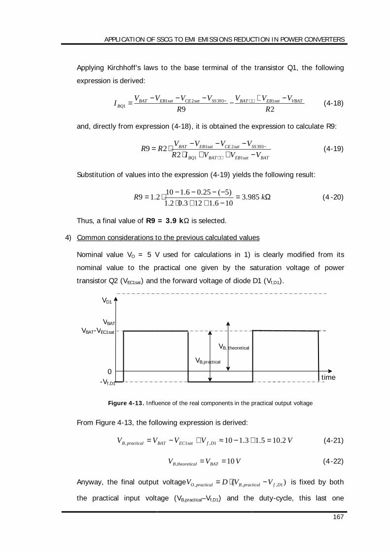
APPLICATION OF SSCG TO EMI EMISSIONS REDUCTION IN POWER CONVERTERS
167
Applying Kirchhoff's laws to the base terminal of the transistor Q1, the following
expression is derived:
29139321
1 RVVV
RVVVVI VBATsatEBBATSSsatCEsatEBBAT
BQ−+
−−−−
= ++− (4-18)
and, directly from expression (4-18), it is obtained the expression to calculate R9:
BATsatEBBATBQ
SSsatCEsatEBBAT
VVVIRVVVVRR
−++⋅−−−
⋅=++
−
11
39321
229 (4-19)
Substitution of values into the expression (4-19) yields the following result:
Ω=−++⋅−−−−
⋅= kR 985.3106.1123.02.1)5(25.06.1102.19 (4 -20)
Thus, a final value of R9 = 3.9 kΩ is selected.
4) Common considerations to the previous calculated values
Nominal value VO = 5 V used for calculations in 1) is clearly modified from its
nominal value to the practical one given by the saturation voltage of power
transistor Q2 (VEC1sat) and the forward voltage of diode D1 (Vf,D1).
Figure 4-13. Influence of the real components in the practical output voltage
From Figure 4-13, the following expression is derived:
VVVVV DfsatECBATpracticalB 2.105.13.1101,1, =+−≈+−= (4-21)
VVV BATltheoreticaB 10, == (4-22)
Anyway, the final output voltage )( 1,,, DfpracticalBpracticalO VVDV −⋅= is fixed by both
the practical input voltage (VB,practical–Vf,D1) and the duty-cycle, this last one
VD1
VBAT
-Vf,D1 0
time
VBAT-VEC1sat
VB,practical
VB, theoretical
APPLICATION OF SSCG TO EMI EMISSIONS REDUCTION IN POWER CONVERTERS
168
depending, mainly, on the turn-on and off times of the power transistor Q1. An
estimated value of ( ) VV practicalO 35.45.12.105.0, =−⋅= is expected at the output of
the power converter. Obviously, apart of these harmonics generated by the fact of
not having a perfect square signal, a duty-cycle not equal to 50% is to produce
even harmonics. This is not important due to the relative comparison between
harmonic amplitudes under the same environment.
The divergence between theoretical and practical output voltages does not affect
the previous calculation where this value was taken into account: it results
negligible respect to this calculations because of the approximate calculations of
the affected components (inductor L, capacitor CO) and the estimations of the
currents through the diode D1 and power transistor Q1.
Another point of interest is the presence of a filter capacitor at the input of supply
terminal such as VBAT and VBAT++ (see Figure 4-3). 470 µF and 22 µF, respectively,
were found experimentally.
Finally, as it was exposed at the end of 1) Calculation of the LC filter, a parallel
combination of two tantalum capacitor each of 22 µF was implemented in the final
circuit.
4.1.2 Frequency modulation generator (UNIT 2)
This frequency modulation stage corresponds properly to the generation of the
modulating waveform to finally control the commutation of the power transistor Q1 at
UNIT 1.
Some attempts have been made along the time to generate easily a frequency
modulation of the PWM signal which controls the commutation of a power transistor.
In reference [RA-1], an integrated circuit UC383 of UNITRODE CORPORATION
(belonging to Texas Instruments) was used. This is a High Speed PWM Controller valid
for switching frequencies up to 1 MHz. It was thought as a fixed switching frequency
controller, whose frequency is set by a resistor connected to pin 5 and a capacitor to
pins 6, 7 (when in conventional or voltage mode). Authors of reference [RA-1]
modified this circuitry slightly in order to obtain a frequency modulated switching
frequency and so, carry out further measurements of EMI emissions. They fixed the
value of capacitor at pins 6,7 but conceived a topology at pin 5 consisting of a parallel
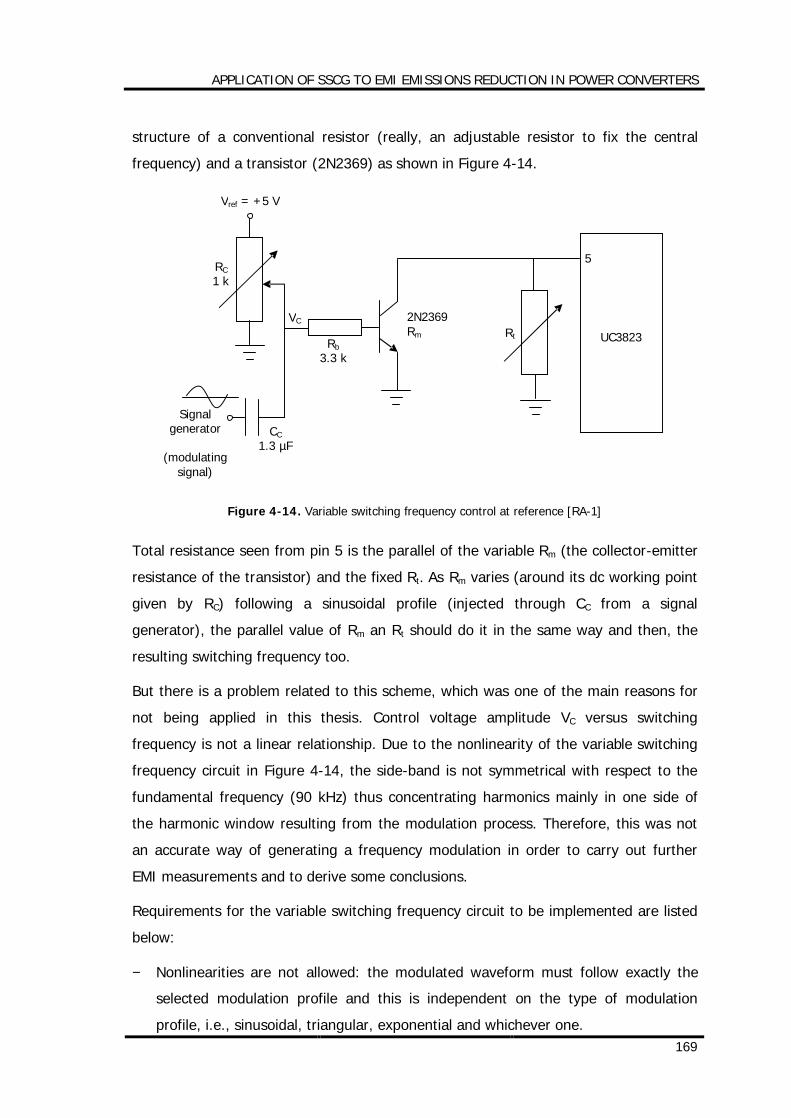
APPLICATION OF SSCG TO EMI EMISSIONS REDUCTION IN POWER CONVERTERS
169
structure of a conventional resistor (really, an adjustable resistor to fix the central
frequency) and a transistor (2N2369) as shown in Figure 4-14.
Figure 4-14. Variable switching frequency control at reference [RA-1]
Total resistance seen from pin 5 is the parallel of the variable Rm (the collector-emitter
resistance of the transistor) and the fixed Rt. As Rm varies (around its dc working point
given by RC) following a sinusoidal profile (injected through CC from a signal
generator), the parallel value of Rm an Rt should do it in the same way and then, the
resulting switching frequency too.
But there is a problem related to this scheme, which was one of the main reasons for
not being applied in this thesis. Control voltage amplitude VC versus switching
frequency is not a linear relationship. Due to the nonlinearity of the variable switching
frequency circuit in Figure 4-14, the side-band is not symmetrical with respect to the
fundamental frequency (90 kHz) thus concentrating harmonics mainly in one side of
the harmonic window resulting from the modulation process. Therefore, this was not
an accurate way of generating a frequency modulation in order to carry out further
EMI measurements and to derive some conclusions.
Requirements for the variable switching frequency circuit to be implemented are listed
below:
− Nonlinearities are not allowed: the modulated waveform must follow exactly the
selected modulation profile and this is independent on the type of modulation
profile, i.e., sinusoidal, triangular, exponential and whichever one.
Signal generator
(modulating
signal)
Vref = +5 V
RC 1 k
CC 1.3 µF
VC
Rb 3.3 k
2N2369 Rm Rt
5
UC3823
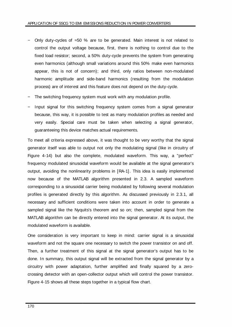
APPLICATION OF SSCG TO EMI EMISSIONS REDUCTION IN POWER CONVERTERS
170
− Only duty-cycles of ≈50 % are to be generated. Main interest is not related to
control the output voltage because, first, there is nothing to control due to the
fixed load resistor; second, a 50% duty-cycle prevents the system from generating
even harmonics (although small variations around this 50% make even harmonics
appear, this is not of concern); and third, only ratios between non-modulated
harmonic amplitude and side-band harmonics (resulting from the modulation
process) are of interest and this feature does not depend on the duty-cycle.
− The switching frequency system must work with any modulation profile.
− Input signal for this switching frequency system comes from a signal generator
because, this way, it is possible to test as many modulation profiles as needed and
very easily. Special care must be taken when selecting a signal generator,
guaranteeing this device matches actual requirements.
To meet all criteria expressed above, it was thought to be very worthy that the signal
generator itself was able to output not only the modulating signal (like in circuitry of
Figure 4-14) but also the complete, modulated waveform. This way, a "perfect"
frequency modulated sinusoidal waveform would be available at the signal generator's
output, avoiding the nonlinearity problems in [RA-1]. This idea is easily implemented
now because of the MATLAB algorithm presented in 2.3. A sampled waveform
corresponding to a sinusoidal carrier being modulated by following several modulation
profiles is generated directly by this algorithm. As discussed previously in 2.3.1, all
necessary and sufficient conditions were taken into account in order to generate a
sampled signal like the Nyquits's theorem and so on; then, sampled signal from the
MATLAB algorithm can be directly entered into the signal generator. At its output, the
modulated waveform is available.
One consideration is very important to keep in mind: carrier signal is a sinusoidal
waveform and not the square one necessary to switch the power transistor on and off.
Then, a further treatment of this signal at the signal generator's output has to be
done. In summary, this output signal will be extracted from the signal generator by a
circuitry with power adaptation, further amplified and finally squared by a zero-
crossing detector with an open-collector output which will control the power transistor.
Figure 4-15 shows all these steps together in a typical flow chart.
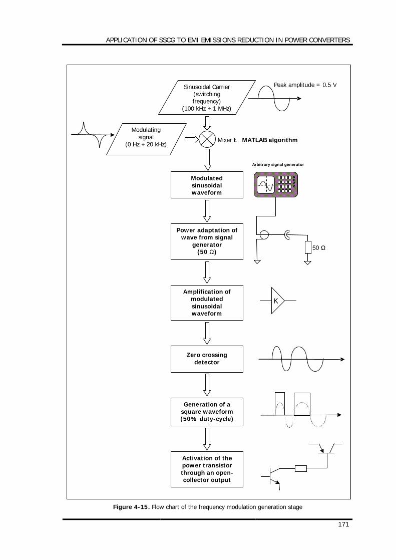
APPLICATION OF SSCG TO EMI EMISSIONS REDUCTION IN POWER CONVERTERS
171
Figure 4-15. Flow chart of the frequency modulation generation stage
Modulated sinusoidal waveform
Zero crossing detector
Generation of a square waveform (50% duty-cycle)
Power adaptation of wave from signal
generator (50 Ω)
Amplification of modulated sinusoidal waveform
Activation of the power transistor through an open-collector output
Modulating signal
(0 Hz ÷ 20 kHz)
Sinusoidal Carrier (switching frequency)
(100 kHz ÷ 1 MHz)
Mixer è MATLAB algorithm
Arbitrary signal generator
K
50 Ω
Peak amplitude = 0.5 V
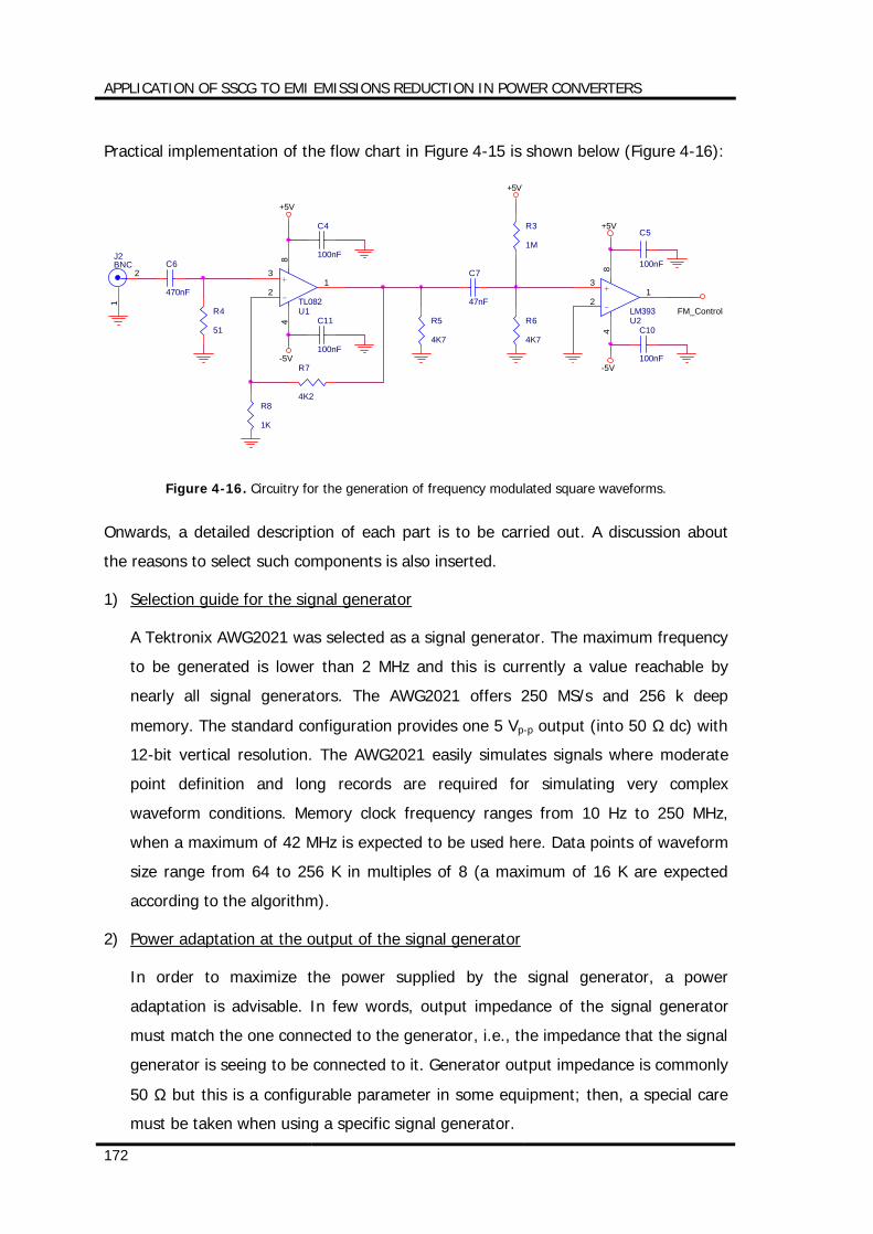
APPLICATION OF SSCG TO EMI EMISSIONS REDUCTION IN POWER CONVERTERS
172
Practical implementation of the flow chart in Figure 4-15 is shown below (Figure 4-16):
+5V
+5V
FM_Control
-5V
+5V
-5V
J2BNC
2
1
+
- LM393U2
3
21
84
+
- TL082U1
3
21
84
R4
51
C4
100nF
R7
4K2
R5
4K7
C7
47nF
R6
4K7
C5
100nFC6
470nF
R3
1M
R8
1K
C11
100nF
C10
100nF
Figure 4-16. Circuitry for the generation of frequency modulated square waveforms.
Onwards, a detailed description of each part is to be carried out. A discussion about
the reasons to select such components is also inserted.
1) Selection guide for the signal generator
A Tektronix AWG2021 was selected as a signal generator. The maximum frequency
to be generated is lower than 2 MHz and this is currently a value reachable by
nearly all signal generators. The AWG2021 offers 250 MS/s and 256 k deep
memory. The standard configuration provides one 5 Vp-p output (into 50 Ω dc) with
12-bit vertical resolution. The AWG2021 easily simulates signals where moderate
point definition and long records are required for simulating very complex
waveform conditions. Memory clock frequency ranges from 10 Hz to 250 MHz,
when a maximum of 42 MHz is expected to be used here. Data points of waveform
size range from 64 to 256 K in multiples of 8 (a maximum of 16 K are expected
according to the algorithm).
2) Power adaptation at the output of the signal generator
In order to maximize the power supplied by the signal generator, a power
adaptation is advisable. In few words, output impedance of the signal generator
must match the one connected to the generator, i.e., the impedance that the signal
generator is seeing to be connected to it. Generator output impedance is commonly
50 Ω but this is a configurable parameter in some equipment; then, a special care
must be taken when using a specific signal generator.
APPLICATION OF SSCG TO EMI EMISSIONS REDUCTION IN POWER CONVERTERS
173
The adaptation stage here proposed is shown in Figure 4-17.
Vo
J2BNC
2
1
R4
50
C6
470nF
VSG
Figure 4-17. Power adaptation stage of the generator's output
Along the whole circuitry, no dc component is expected to be present on the signal.
To guarantee this aspect, several configurations have been assumed along the
circuit. At this adaptation stage, a capacitor is provided in order to block the
possible dc component coming from the signal generator. Any offset due to an
undesirable dc component must be blocked by this capacitor but it must allow the
FM signal to flow through it with nearly no attenuation.
In order to get an impedance of 50 Ω, capacitor C6 should have a short-circuit
behaviour at the frequencies of interest, that is, from 100 kHz onwards. As
concluded from the observation of Figure 4-16, the next stage following this
adaptation module is an operational amplifier, showing an input impedance (over
1012 Ω) much more higher than 50 Ω. This next stage can be assumed as an open-
circuit what makes the calculations easier because of the non-influence between
stages in cascade.
Waveform coming from the signal generator has peak amplitude of 0.5 V, that is, a
peak-to-peak amplitude of 1 V. Voltage across R4 (Vo=VR4) is given by the
following expression:
( )26421
642
CRf
CRfVV SGo⋅⋅⋅⋅+
⋅⋅⋅⋅⋅=
π
π (4-23)
where VSG represents the amplitude of the signal generator output.
Although the minimum central frequency under test is 100 kHz, calculation of
capacitor C6 is to be done for a much lower frequency (e.g., 50 kHz) in order to
absorb all possible frequency deviations due to the modulation process. Please
consider the following data:
− f = 50 kHz

APPLICATION OF SSCG TO EMI EMISSIONS REDUCTION IN POWER CONVERTERS
174
− ratio SG
o
VV
must be over ≈99% è no signal attenuation is present due to C6.
− R4 = 50 Ω
Proper operation over expression (4-23) together with the values above yields a
value of C6 = 470 nF. This is the minimum value acceptable for this capacitor C6.
3) Amplification of the waveform after the power adaptation stage
At this stage, a signal without dc component should be present, with peak
amplitude of ≈0.25 V (due to the voltage divisor of the previous adaptation stage).
It must also be said that this stage is not mandatory to be implemented if the
signal generator is able to give out an approximate Vpp > 2 V at its output, because
the response delay time of the next stage (comparator) is depending on the signal
excursion at its input. Then, in order to have the chance to connect any signal
generator system, an amplification stage was included in this prototype.
A maximum frequency of 1.1 MHz is expected at the input of the operational
amplifier. This corresponds to a 1MHz-carrier frequency modulated by a modulation
signal with a percentage of modulation equal to 10%.
The main part of this stage consists of an operational amplifier in a typical non-
inverting configuration.
Vin
-5V
+5V
Vout
+
- TL082U1
3
21
84
C4
100nF
R7
4K2
R5
4K7
R8
1K
C11
100nF
Figure 4-18. Non-inverting amplification configuration after power adaptation stage
As seen in Figure 4-18, a TL082 of National Semiconductor was selected. The next
considerations made this decision reasonable:
APPLICATION OF SSCG TO EMI EMISSIONS REDUCTION IN POWER CONVERTERS
175
− The TL082 offers a typical gain-bandwidth product of 4 MHz, enough for this
application. Considering that a gain of ≈5 is configured and the maximum
frequency present in the system is lower than 1.1 MHz, the practical gain-
bandwidth product is 5×1.1MHZ = 5.5 MHz. This is, of course, higher than the
typical 4 MHz, which means an attenuation of the output amplitude (i.e., an
actual gain lower than the theoretical value of 5). This does not represent any
problems because, despite this undesirable attenuation at limit values, the
amplifier output amplitude will be large enough to activate the comparator
input at the next stage.
− A dual supply voltage is mandatory.
− The maximum slew-rate for a sinusoidal waveform is expressed by
fASR ⋅⋅⋅= π2 (SR = Slew-rate in V/µs, A = peak amplitude in V and f =
frequency in MHz). In this prototype, the maximum slew-rate takes place under
the following limit circumstances: A = 0.25 V and f = 1.1 MHz, yielding a slew-
rate of 1.728 V/µs. However, TL082 offers a typical 13 V/µs, large enough for
the actual purposes.
− A total harmonic distortion lower than 0.02%, a typical Common-Mode
Rejection Ratio (CMRR) of 100 dB and a typical Power Supply Rejection Ratio
(PSRR) of 100 dB are available at TL082, meeting completely all necessities.
− Finally, from the logistic point of view, this is a typical component, easy to find.
Design philosophy is to build a practical system but using the commonest,
cheapest and simplest components.
Voltage gain of the configuration in Figure 4-18 is calculated as follows:
871
3
5
RR
VV
VV
pin
R
in
out +== (4-24)
For the selected values (R7 = 4.2 kΩ, R8 = 1 kΩ), a theoretical gain of 5.2 is
expected. Taking into account that the expected peak-value at the amplifier input
(pin 3) is 0.25 V, a peak-value of 1.3 V is to be found at the amplifier output,
across the resistor R5, a load resistor intended for amplifier stabilization subjects.
Amplitude values at the amplifier output are strongly related to the behaviour of
the voltage comparator at the next stage. The larger voltage excursion at the
comparator input, the faster response time.
APPLICATION OF SSCG TO EMI EMISSIONS REDUCTION IN POWER CONVERTERS
176
Two de-coupling capacitors (100 nF) are also inserted in order to filter and stabilize
the power supply pins of this operational amplifier.
Along the whole circuitry, no dc component is expected to be present on the signal.
4) Square waveform generation
The configuration to generate a square waveform from a sinusoidal one is shown in
Figure 4-19. It consists of a typical zero-crossing detection stage, when a dual-
supply comparator is to use.
A LM393 of National Semiconductor was selected for this stage due to the following
reasons:
− High precision comparators.
− Allow sensing near ground (very useful when detection of zero-crossing).
− Offer an integrated open-collector output.
− When a large signal excursion (>>100 mV) is present at the input of the
comparator, a typical response time of 300 ns is available, enough for the
actual timing considerations. As calculated in the previous stage, a peak-to-
peak excursion of 2.6 V is to be expected at the amplifier output and, therefore,
after crossing the coupling capacitor C7, at the comparator input.
− Finally, as expressed previously, this is a typical component, easy to find, so
keeping the design philosophy of building a practical system but using the
commonest, cheapest and simplest components.
+5V
+5V
Voa
FM_Control
-5V
+
- LM393U2
3
21
84
R6
4K7
C5
100nF
R3
1M
C10
100nF
C7
47nF
Figure 4-19. Square-wave generation configuration after the amplification stage
APPLICATION OF SSCG TO EMI EMISSIONS REDUCTION IN POWER CONVERTERS
177
The couple of resistors R3 and R6 is intended for generating a very low offset at
the input + of the comparator. When no signal is present along the system, it must
be guaranteed a voltage at pin 3 slightly higher than voltage at pin 2, i.e., voltage
at pin 3 must be slightly over Ground. This way, it is assured that the open-
collector output (FM_Control) is cut-off and activation of the power transistor Q1 is
not possible. If FM_Control were always activated (low level), power transistor Q1
would also be turned on, then supplying the input VBAT voltage directly to the load
resistor, causing probably the destruction of both transistor and load resistor.
Voltage at pin 3 (Vpin3) for the selected values in Figure 4-19 yields the following
value:
63653 RR
RVVpin +⋅+= (4 -25)
mVVV pin 4.237.41000
7.453 =+
⋅+=
that is, large enough to produce an offset but negligible for the peak-to-peak
expected signal voltage of 2.6 V at pin 3.
At the input of this stage, a coupling capacitor is provided in order to block the
possible dc component coming from the previous amplification stage. Any offset
due to an undesirable dc component must be blocked by this capacitor but it must
allow the FM signal to flow through it with nearly no attenuation.
Although the minimum central frequency under test is 100 kHz, calculation of
capacitor C7 is to be done for a much lower frequency (e.g., 50 kHz) in order to
absorb all possible frequency deviations due to the modulation process. Consider
the following data in Figure 4-19:
− f = 50 kHz
− ratio oa
pin
VV 3 must be kept over ≈99%, where Vpin3 is the input voltage at pin 3 of
the comparator and Voa, the voltage from the operational amplifier output è no
signal attenuation is present due to the capacitor.
− Rpar = R3//R6 = 1MΩ//4.7kΩ = 4.678 kΩ. The input impedance of pin 3 is
much higher than this value of Rpar; therefore, considering only the value of Rpar
for the filter calculation is enough.

APPLICATION OF SSCG TO EMI EMISSIONS REDUCTION IN POWER CONVERTERS
178
Voltage at pin 3 can be therefore calculated as follows:
( )23721
72
CRf
CRfVV
par
paroapin
⋅⋅⋅⋅+
⋅⋅⋅⋅⋅=
π
π (4 -26)
Proper operation over expression (4-26) together with the values listed above
yields a value of C7 = 47 nF. This represents an estimation of the minimum value
acceptable for this capacitor.
Finally, two de-coupling capacitors (100 nF) are also inserted in order to filter and
stabilize the power supply pins of this voltage comparator.
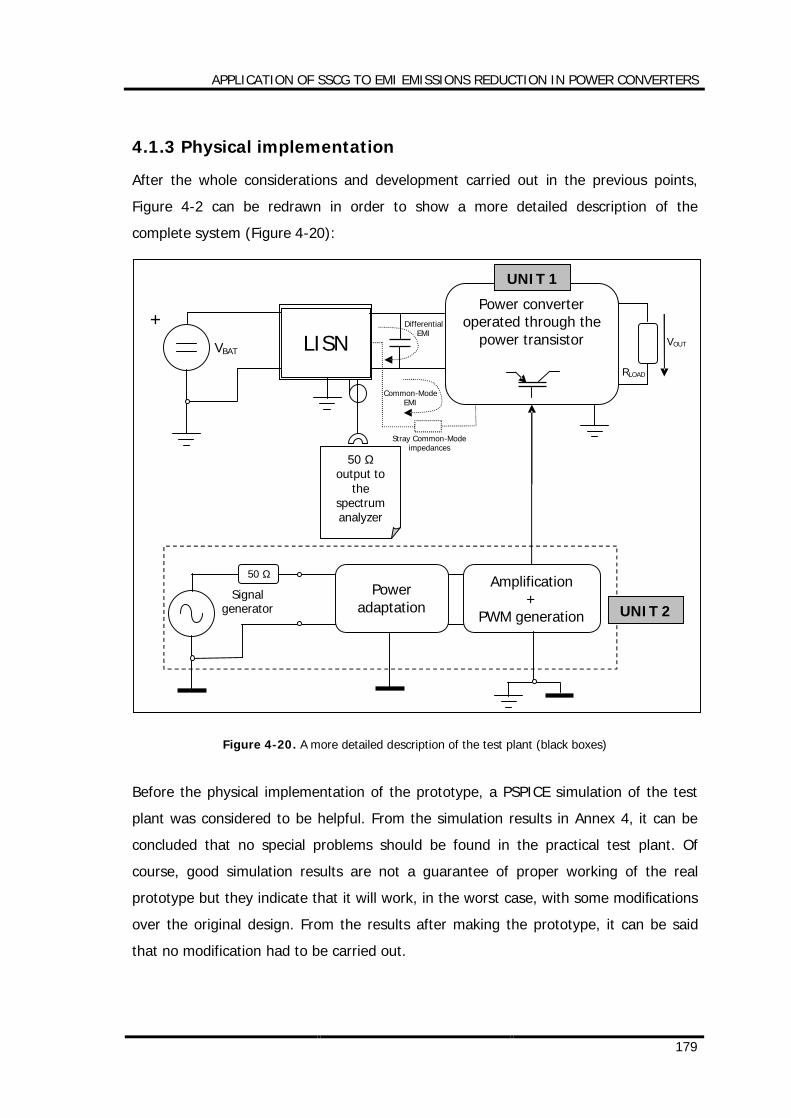
APPLICATION OF SSCG TO EMI EMISSIONS REDUCTION IN POWER CONVERTERS
179
4.1.3 Physical implementation
After the whole considerations and development carried out in the previous points,
Figure 4-2 can be redrawn in order to show a more detailed description of the
complete system (Figure 4-20):
Figure 4-20. A more detailed description of the test plant (black boxes)
Before the physical implementation of the prototype, a PSPICE simulation of the test
plant was considered to be helpful. From the simulation results in Annex 4, it can be
concluded that no special problems should be found in the practical test plant. Of
course, good simulation results are not a guarantee of proper working of the real
prototype but they indicate that it will work, in the worst case, with some modifications
over the original design. From the results after making the prototype, it can be said
that no modification had to be carried out.
Power converter operated through the
power transistor LISN +
Amplification +
PWM generation
50 Ω output to
the spectrum analyzer
RLOAD
VBAT
UNIT 2
VOUT
50 Ω
Power adaptation
Signal generator
Differential
EMI
Common-Mode EMI
Stray Common-Mode impedances
UNIT 1
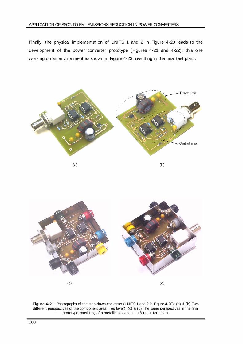
APPLICATION OF SSCG TO EMI EMISSIONS REDUCTION IN POWER CONVERTERS
180
Finally, the physical implementation of UNITS 1 and 2 in Figure 4-20 leads to the
development of the power converter prototype (Figures 4-21 and 4-22), this one
working on an environment as shown in Figure 4-23, resulting in the final test plant.
(a) (b)
(c) (d)
Figure 4-21. Photographs of the step-down converter (UNITS 1 and 2 in Figure 4-20): (a) & (b) Two different perspectives of the component area (Top layer); (c) & (d) The same perspectives in the final
prototype consisting of a metallic box and input/output terminals.
Control area
Power area
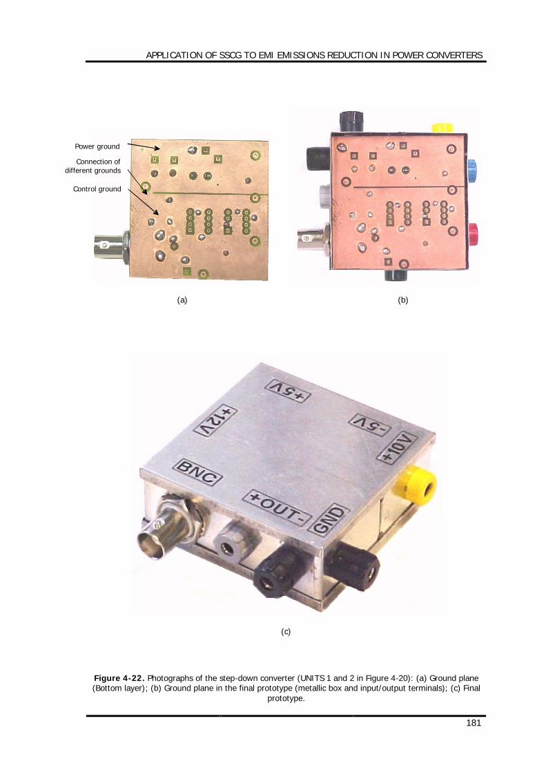
APPLICATION OF SSCG TO EMI EMISSIONS REDUCTION IN POWER CONVERTERS
181
(a) (b)
(c)
Figure 4-22. Photographs of the step-down converter (UNITS 1 and 2 in Figure 4-20): (a) Ground plane (Bottom layer); (b) Ground plane in the final prototype (metallic box and input/output terminals); (c) Final
prototype.
Power ground
Control ground
Connection of different grounds
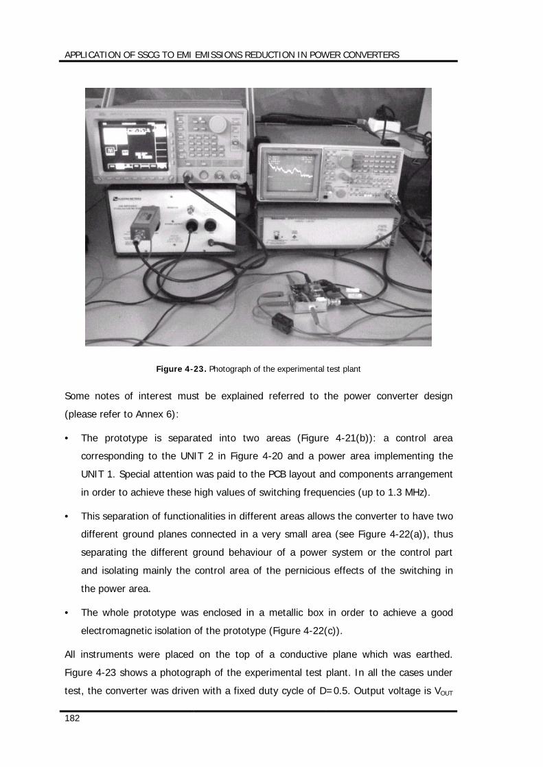
APPLICATION OF SSCG TO EMI EMISSIONS REDUCTION IN POWER CONVERTERS
182
Figure 4-23. Photograph of the experimental test plant
Some notes of interest must be explained referred to the power converter design
(please refer to Annex 6):
• The prototype is separated into two areas (Figure 4-21(b)): a control area
corresponding to the UNIT 2 in Figure 4-20 and a power area implementing the
UNIT 1. Special attention was paid to the PCB layout and components arrangement
in order to achieve these high values of switching frequencies (up to 1.3 MHz).
• This separation of functionalities in different areas allows the converter to have two
different ground planes connected in a very small area (see Figure 4-22(a)), thus
separating the different ground behaviour of a power system or the control part
and isolating mainly the control area of the pernicious effects of the switching in
the power area.
• The whole prototype was enclosed in a metallic box in order to achieve a good
electromagnetic isolation of the prototype (Figure 4-22(c)).
All instruments were placed on the top of a conductive plane which was earthed.
Figure 4-23 shows a photograph of the experimental test plant. In all the cases under
test, the converter was driven with a fixed duty cycle of D=0.5. Output voltage is VOUT
APPLICATION OF SSCG TO EMI EMISSIONS REDUCTION IN POWER CONVERTERS
183
≈ 4V (instead of the expected 5 V, due to the diode forward voltage drop) and the
power supplied by this converter is ≈1.25W.
4.2 Influence of the Spectrum Analyzer's RBW
In order to show the influence of regulatory RBWs when measuring EMI emissions,
some of the previous modulations were used in the power converter presented in
clause 4.1 based on a step-down topology. A previously modulated sinusoidal wave,
generated numerically [RB-1], is stored in a compliant Arbitrary Function Generator
(Tektronix AWG2021). To generate a proper PWM signal controlling the power switch
(transistor), a previous stage of signal adaptation, amplification and zero-crossing
detection is implemented to square the previous sinusoidal wave but preserving the
current modulation. This way, a modulated square signal (≈50%-duty cycle) is also
obtained at the input of the step-down converter (VBAT = 10 V and RLOAD = 20 Ω).
Conducted emissions are measured by a compliant spectrum analyzer (Tektronix 2712)
by means of a monophase-LISN, whose schema is shown in Figure 4-24:
Figure 4-24. Schema of the compliant monophase-LISN used for measurements in the thesis
(NOTE: EUT=Equipment Under Test)
The boundary between Band A and B in CISPR22 & 16-1 is set to 150 kHz, also fixing
the RBW to be adjusted. For a 120kHz-switching frequency, a 200Hz-RBW is to be
used; however, a few kHz upwards (at 200 kHz) this RBW is fixed to 9 kHz
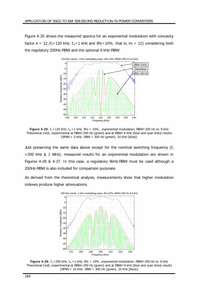
APPLICATION OF SSCG TO EMI EMISSIONS REDUCTION IN POWER CONVERTERS
184
Figure 4-25 shows the measured spectra for an exponential modulation with concavity
factor k = 12 (fc=120 kHz, fm=1 kHz and δ%=10%, that is, mf = 12) considering both
the regulatory 200Hz-RBW and the optional 9 kHz-RBW.
100 105 110 115 120 125 130 135 140
-50
-45
-40
-35
-30
-25
-20
-15
-10
-5
0
Frequency (kHz)
Rel
ativ
e Am
plitu
de (d
BV)
120 kHz carrier, 1 kHz modulating wave, d%=10%, RBW=200 Hz & 9 kHz
Figure 4-25. fc =120 kHz, fm =1 kHz, δ% = 10%, exponential modulation, RBW=200 Hz vs. 9 kHz Theoretical (red), experimental at RBW=200 Hz (green) and at RBW=9 kHz (blue and cyan lines) results
(SPAN = 5 kHz, VBW = 300 Hz (green), 10 kHz (blue))
Just preserving the same data above except for the nominal switching frequency (fc
=200 kHz & 1 MHz), measured results for an exponential modulation are shown in
Figures 4-26 & 4-27. In this case, a regulatory 9kHz-RBW must be used although a
200Hz-RBW is also included for comparison purposes.
As derived from the theoretical analysis, measurements show that higher modulation
indexes produce higher attenuations.
170 180 190 200 210 220 230-50
-45
-40
-35
-30
-25
-20
-15
-10
-5
0
Frequency (kHz)
Rel
ativ
e Am
plitu
de (d
BV)
200 kHz carrier, 1 kHz modulating wave, d%=10%, RBW=200 Hz & 9 kHz
Figure 4-26. fc =200 kHz, fm =1 kHz, δ% = 10%, exponential modulation, RBW=200 Hz vs. 9 kHz
Theoretical (red), experimental at RBW=200 Hz (green) and at RBW=9 kHz (blue and cyan lines) results (SPAN = 10 kHz, VBW = 300 Hz (green), 10 kHz (blue))
RBW=9 kHz
RBW=200 Hz
Theoretical
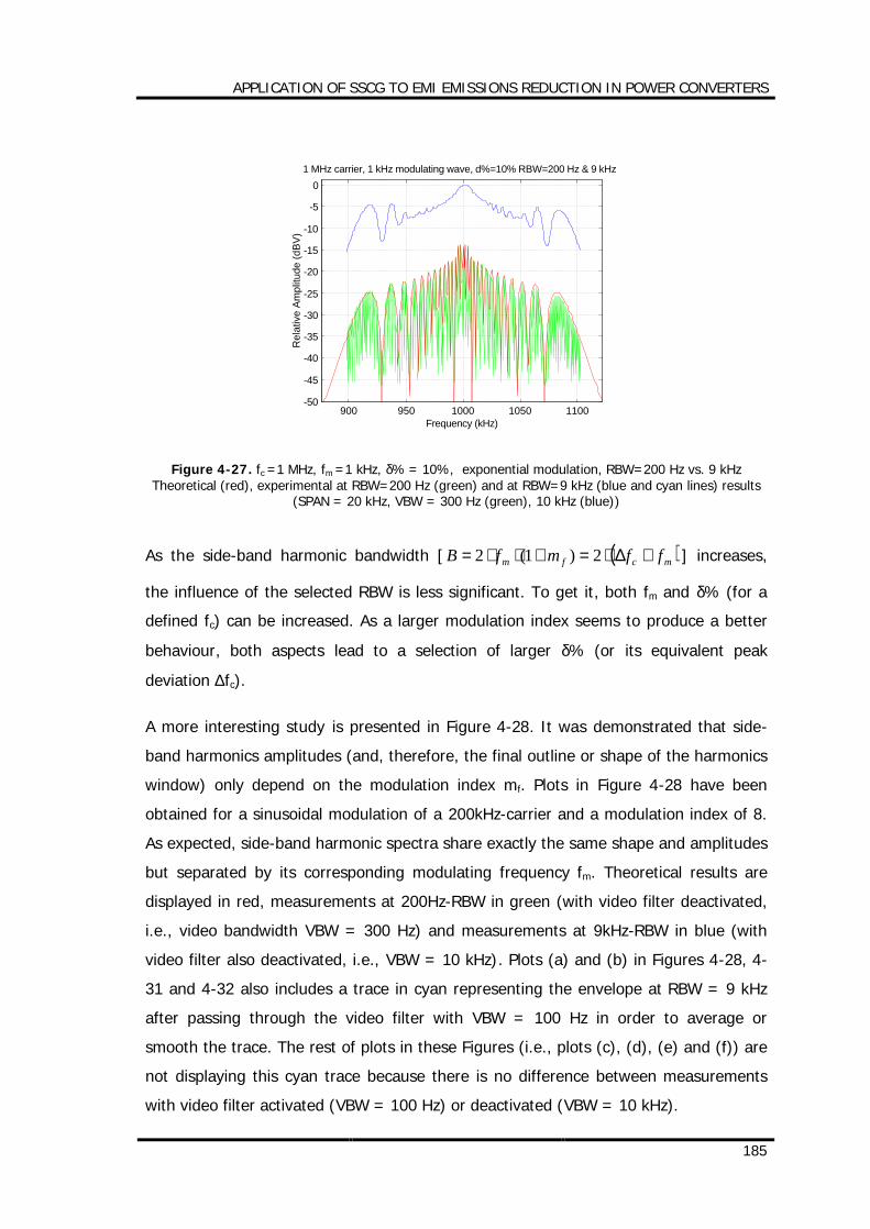
APPLICATION OF SSCG TO EMI EMISSIONS REDUCTION IN POWER CONVERTERS
185
900 950 1000 1050 1100-50
-45
-40
-35
-30
-25
-20
-15
-10
-5
0
Frequency (kHz)
Rel
ativ
e Am
plitu
de (d
BV)
1 MHz carrier, 1 kHz modulating wave, d%=10% RBW=200 Hz & 9 kHz
Figure 4-27. fc =1 MHz, fm =1 kHz, δ% = 10%, exponential modulation, RBW=200 Hz vs. 9 kHz Theoretical (red), experimental at RBW=200 Hz (green) and at RBW=9 kHz (blue and cyan lines) results
(SPAN = 20 kHz, VBW = 300 Hz (green), 10 kHz (blue))
As the side-band harmonic bandwidth [ ( )mcfm ffmfB +∆⋅=+⋅⋅= 2)1(2 ] increases,
the influence of the selected RBW is less significant. To get it, both fm and δ% (for a
defined fc) can be increased. As a larger modulation index seems to produce a better
behaviour, both aspects lead to a selection of larger δ% (or its equivalent peak
deviation ∆fc).
A more interesting study is presented in Figure 4-28. It was demonstrated that side-
band harmonics amplitudes (and, therefore, the final outline or shape of the harmonics
window) only depend on the modulation index mf. Plots in Figure 4-28 have been
obtained for a sinusoidal modulation of a 200kHz-carrier and a modulation index of 8.
As expected, side-band harmonic spectra share exactly the same shape and amplitudes
but separated by its corresponding modulating frequency fm. Theoretical results are
displayed in red, measurements at 200Hz-RBW in green (with video filter deactivated,
i.e., video bandwidth VBW = 300 Hz) and measurements at 9kHz-RBW in blue (with
video filter also deactivated, i.e., VBW = 10 kHz). Plots (a) and (b) in Figures 4-28, 4-
31 and 4-32 also includes a trace in cyan representing the envelope at RBW = 9 kHz
after passing through the video filter with VBW = 100 Hz in order to average or
smooth the trace. The rest of plots in these Figures (i.e., plots (c), (d), (e) and (f)) are
not displaying this cyan trace because there is no difference between measurements
with video filter activated (VBW = 100 Hz) or deactivated (VBW = 10 kHz).
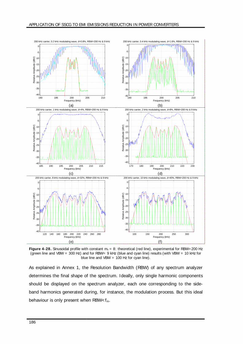
APPLICATION OF SSCG TO EMI EMISSIONS REDUCTION IN POWER CONVERTERS
186
190 195 200 205 210-40
-35
-30
-25
-20
-15
-10
-5
0
Frequency (kHz)
Rel
ativ
e Am
plitu
de (d
BV)
200 kHz carrier, 0.2 kHz modulating wave, d=0.8%, RBW=200 Hz & 9 kHz
(a)
190 195 200 205 210-40
-35
-30
-25
-20
-15
-10
-5
0
Frequency (kHz)
Rel
ativ
e Am
plitu
de (d
BV)
200 kHz carrier, 0.4 kHz modulating wave, d=1.6%, RBW=200 Hz & 9 kHz
(b)
185 190 195 200 205 210 215-40
-35
-30
-25
-20
-15
-10
-5
0
Frequency (kHz)
Rel
ativ
e Am
plitu
de (d
BV)
200 kHz carrier, 1 kHz modulating wave, d=4%, RBW=200 Hz & 9 kHz
(c)
170 180 190 200 210 220 230-40
-35
-30
-25
-20
-15
-10
-5
0
Frequency (kHz)
Rel
ativ
e Am
plitu
de (d
BV)
200 kHz carrier, 2 kHz modulating wave, d=8%, RBW=200 Hz & 9 kHz
(d)
120 140 160 180 200 220 240 260 280-40
-35
-30
-25
-20
-15
-10
-5
0
Frequency (kHz)
Rel
ativ
e Am
plitu
de (d
BV)
200 kHz carrier, 8 kHz modulating wave, d=32%, RBW=200 Hz & 9 kHz
(e)
100 150 200 250 300
-40
-35
-30
-25
-20
-15
-10
-5
0
Frequency (kHz)
Rel
ativ
e Am
plitu
de (d
BV)
200 kHz carrier, 10 kHz modulating wave, d=40%, RBW=200 Hz & 9 kHz
(f)
Figure 4-28. Sinusoidal profile with constant mf = 8: theoretical (red line), experimental for RBW=200 Hz (green line and VBW = 300 Hz) and for RBW= 9 kHz (blue and cyan line) results (with VBW = 10 kHz for
blue line and VBW = 100 Hz for cyan line).
As explained in Annex 1, the Resolution Bandwidth (RBW) of any spectrum analyzer
determines the final shape of the spectrum. Ideally, only single harmonic components
should be displayed on the spectrum analyzer, each one corresponding to the side-
band harmonics generated during, for instance, the modulation process. But this ideal
behaviour is only present when RBW<fm.
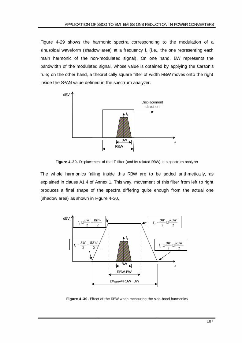
APPLICATION OF SSCG TO EMI EMISSIONS REDUCTION IN POWER CONVERTERS
187
Figure 4-29 shows the harmonic spectra corresponding to the modulation of a
sinusoidal waveform (shadow area) at a frequency fc (i.e., the one representing each
main harmonic of the non-modulated signal). On one hand, BW represents the
bandwidth of the modulated signal, whose value is obtained by applying the Carson's
rule; on the other hand, a theoretically square filter of width RBW moves onto the right
inside the SPAN value defined in the spectrum analyzer.
Figure 4-29. Displacement of the IF-filter (and its related RBW) in a spectrum analyzer
The whole harmonics falling inside this RBW are to be added arithmetically, as
explained in clause A1.4 of Annex 1. This way, movement of this filter from left to right
produces a final shape of the spectra differing quite enough from the actual one
(shadow area) as shown in Figure 4-30.
Figure 4-30. Effect of the RBW when measuring the side-band harmonics
BW
BWRBW=RBW+BW
f
dBV
fc
22RBWBWf c −−
22RBWBWf c ++
22RBWBWf c −+
22RBWBWf c +−
RBW-BW
BW
RBW f
dBV
fc
Displacement direction
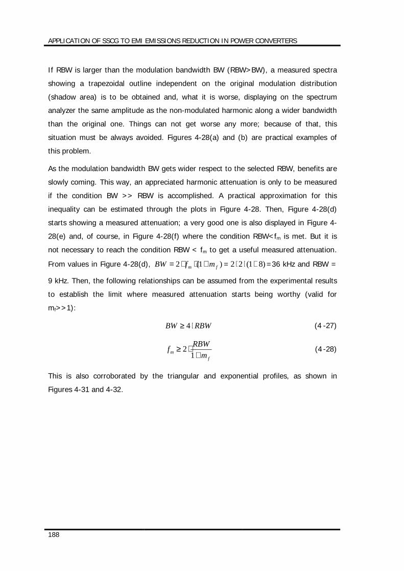
APPLICATION OF SSCG TO EMI EMISSIONS REDUCTION IN POWER CONVERTERS
188
If RBW is larger than the modulation bandwidth BW (RBW>BW), a measured spectra
showing a trapezoidal outline independent on the original modulation distribution
(shadow area) is to be obtained and, what it is worse, displaying on the spectrum
analyzer the same amplitude as the non-modulated harmonic along a wider bandwidth
than the original one. Things can not get worse any more; because of that, this
situation must be always avoided. Figures 4-28(a) and (b) are practical examples of
this problem.
As the modulation bandwidth BW gets wider respect to the selected RBW, benefits are
slowly coming. This way, an appreciated harmonic attenuation is only to be measured
if the condition BW >> RBW is accomplished. A practical approximation for this
inequality can be estimated through the plots in Figure 4-28. Then, Figure 4-28(d)
starts showing a measured attenuation; a very good one is also displayed in Figure 4-
28(e) and, of course, in Figure 4-28(f) where the condition RBW<fm is met. But it is
not necessary to reach the condition RBW < fm to get a useful measured attenuation.
From values in Figure 4-28(d), )1(2 fm mfBW +⋅⋅= = )81(22 +⋅⋅ =36 kHz and RBW =
9 kHz. Then, the following relationships can be assumed from the experimental results
to establish the limit where measured attenuation starts being worthy (valid for
mf>>1):
RBWBW ⋅≥ 4 (4 -27)
fm m
RBWf+
⋅≥1
2 (4 -28)
This is also corroborated by the triangular and exponential profiles, as shown in
Figures 4-31 and 4-32.
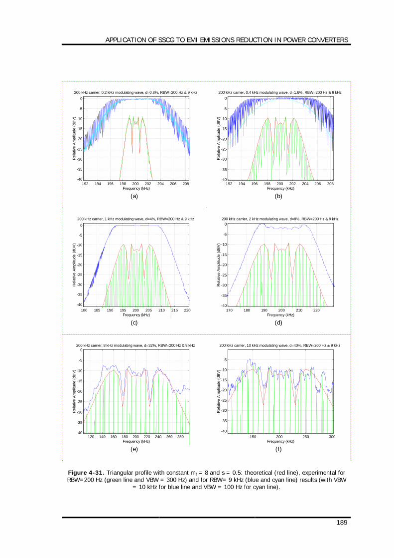
APPLICATION OF SSCG TO EMI EMISSIONS REDUCTION IN POWER CONVERTERS
189
192 194 196 198 200 202 204 206 208-40
-35
-30
-25
-20
-15
-10
-5
0
Frequency (kHz)
Rel
ativ
e Am
plitu
de (d
BV)
200 kHz carrier, 0.2 kHz modulating wave, d=0.8%, RBW=200 Hz & 9 kHz
(a)
192 194 196 198 200 202 204 206 208-40
-35
-30
-25
-20
-15
-10
-5
0
Frequency (kHz)
Rel
ativ
e Am
plitu
de (d
BV)
200 kHz carrier, 0.4 kHz modulating wave, d=1.6%, RBW=200 Hz & 9 kHz
(b)
180 185 190 195 200 205 210 215 220-40
-35
-30
-25
-20
-15
-10
-5
0
Frequency (kHz)
Rel
ativ
e Am
plitu
de (d
BV)
200 kHz carrier, 1 kHz modulating wave, d=4%, RBW=200 Hz & 9 kHz
(c)
170 180 190 200 210 220-40
-35
-30
-25
-20
-15
-10
-5
0
Frequency (kHz)
Rel
ativ
e Am
plitu
de (d
BV)
200 kHz carrier, 2 kHz modulating wave, d=8%, RBW=200 Hz & 9 kHz
(d)
120 140 160 180 200 220 240 260 280-40
-35
-30
-25
-20
-15
-10
-5
0
Frequency (kHz)
Rel
ativ
e Am
plitu
de (d
BV)
200 kHz carrier, 8 kHz modulating wave, d=32%, RBW=200 Hz & 9 kHz
(e)
150 200 250 300-40
-35
-30
-25
-20
-15
-10
-5
Frequency (kHz)
Rel
ativ
e Am
plitu
de (d
BV)
200 kHz carrier, 10 kHz modulating wave, d=40%, RBW=200 Hz & 9 kHz
(f)
Figure 4-31. Triangular profile with constant mf = 8 and s = 0.5: theoretical (red line), experimental for RBW=200 Hz (green line and VBW = 300 Hz) and for RBW= 9 kHz (blue and cyan line) results (with VBW
= 10 kHz for blue line and VBW = 100 Hz for cyan line).
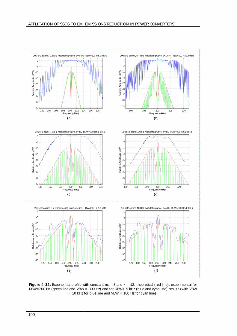
APPLICATION OF SSCG TO EMI EMISSIONS REDUCTION IN POWER CONVERTERS
190
192 194 196 198 200 202 204 206 208-40
-35
-30
-25
-20
-15
-10
-5
0
Frequency (kHz)
Rel
ativ
e Am
plitu
de (d
BV)
200 kHz carrier, 0.2 kHz modulating wave, d=0.8%, RBW=200 Hz & 9 kHz
(a)
190 195 200 205 210
-40
-35
-30
-25
-20
-15
-10
-5
0
Frequency (kHz)
Rel
ativ
e Am
plitu
de (d
BV)
200 kHz carrier, 0.4 kHz modulating wave, d=1.6%, RBW=200 Hz & 9 kHz
(b)
185 190 195 200 205 210 215-40
-35
-30
-25
-20
-15
-10
-5
0
Frequency (kHz)
Rel
ativ
e Am
plitu
de (d
BV)
200 kHz carrier, 1 kHz modulating wave, d=4%, RBW=200 Hz & 9 kHz
(c)
170 180 190 200 210 220-40
-35
-30
-25
-20
-15
-10
-5
0
Frequency (kHz)
Rel
ativ
e Am
plitu
de (d
BV)
200 kHz carrier, 2 kHz modulating wave, d=8%, RBW=200 Hz & 9 kHz
(d)
120 140 160 180 200 220 240 260 280-40
-35
-30
-25
-20
-15
-10
-5
0
Frequency (kHz)
Rel
ativ
e Am
plitu
de (d
BV)
200 kHz carrier, 8 kHz modulating wave, d=32%, RBW=200 Hz & 9 kHz
(e)
120 140 160 180 200 220 240 260 280-40
-35
-30
-25
-20
-15
-10
-5
0
Frequency (kHz)
Rel
ativ
e Am
plitu
de (d
BV)
200 kHz carrier, 10 kHz modulating wave, d=40%, RBW=200 Hz & 9 kHz
(f)
Figure 4-32. Exponential profile with constant mf = 8 and k = 12: theoretical (red line), experimental for RBW=200 Hz (green line and VBW = 300 Hz) and for RBW= 9 kHz (blue and cyan line) results (with VBW
= 10 kHz for blue line and VBW = 100 Hz for cyan line).
APPLICATION OF SSCG TO EMI EMISSIONS REDUCTION IN POWER CONVERTERS
191
4.3 Proposal of a practical method to select a valuable SSCG
technique applied to Switching Power Converters
All theoretical developments and practical considerations presented along this thesis
allow now to present this point: how to select a worthy SSCG method for a switching
power supply, i.e., the modulation profile, the switching frequency and its peak
deviation through the percentage of modulation and the modulating frequency in order
to obtain normative benefits. It is important to distinguish between a phenomenon
itself and the way it is going to be measured. Although theoretical results show a good
performance of frequency modulation regarding to EMI emissions reduction in every
case, measurements procedures (normally related to practical limitations of measure
equipment or normative aspects) can fade such a good behaviour even making it
negligible. In other words, a good theoretical SSCG system is not a guarantee of a
good experimental result when measuring according to normative regulations: this
aspect is desired to solve with this selection proposal.
It consists of several steps as shown in Figure 4-34, steps which are to be developed
onwards.
STEP 1: Selection of the modulation profile
(Please refer to previous comments and results already presented in clause 3.4).
Considering the global behaviour of the modulation, the most important parameter
is Fenv,peak. It provides a very useful information because of its global characteristic:
the maximum amplitude (respect to the non-modulated carrier frequency) along the
whole spectrum distribution as a result of a frequency modulation, that is, all
harmonic amplitudes will be under this value Fenv,peak. If the number of new
harmonics generated during the modulation process is not of concern but only their
amplitudes, this parameter Fenv,peak should be the target. Then, a flat harmonic
distribution is the most profitable and, therefore, a triangular modulation profile is
the most suitable for any application with these characteristics. Exponential profile
shows the worst behaviour because of the peak shape of the side-band harmonic
distribution. If attenuation given by an exponential profile at a certain modulation
index mf is found to be satisfactory, then it can be a good option because the side-
band harmonics decrease fast as the side-harmonic order gets farther from the
central frequency.
APPLICATION OF SSCG TO EMI EMISSIONS REDUCTION IN POWER CONVERTERS
192
Because Fenv,peak does not oscillate too much, main efforts should be concentrated
on obtaining a cancellation of a certain harmonic, normally, the one at the carrier
frequency, that is, it is desired a value of F1 = 0 V or, in a practical case, F1 < -40
dBV (relative to the non-modulated carrier signal). To do this, a special profit of the
oscillation features of the value F1 is to be taken. Working points should be selected
at those modulation indexes where harmonic cancellation is available.
Anyway, modulation profile to be selected is depending on the systems necessities
or exigencies and no generic formula can be given.
STEP 2: Selection of the modulation index mf
Theoretical analysis carried out in the previous sections for several modulation
profiles makes now an easy task to choose the modulation index necessary to
achieve a certain attenuation. Please refer to all comments and results presented
along the chapter 3.
STEP 3: Selection of the switching (carrier) frequency fc
For designs already in use, where it is of interest substituting the current constant
switching frequency for a new frequency modulated by a SSCG method, this is an
imposed parameter; for new designs, this is one of the most important parameters
to be selected. Switching (carrier) frequency in power converters is not usually too
large because the electronics components (diodes and power transistors, mainly)
are not able to manage larger power with shorter switching times. Please review
related considerations already presented in clause 3.6.
STEPS 4 & 5: Selection of the normative RBW and the modulating frequency fm
Although higher switching frequencies are always of interest (due to their benefits
of lower converter size and higher efficiencies), a special care must be taken
respect to the Spectrum Analyzer's RBW. The associated normative (both FCC and
CISPR-22) was already presented in detail in clause A2.3 (Annex2), where it is
clearly defined the RBW to be used at every frequency range or band. Because
power converters switching frequencies are normally below 30 MHz (the boundary
between bands B and C [RE-1]), there are only two possible RBWs of interest in
switching power converters: 200 Hz (band A) and 9 kHz (band B). The boundary
between these two bands is set to 150 kHz.
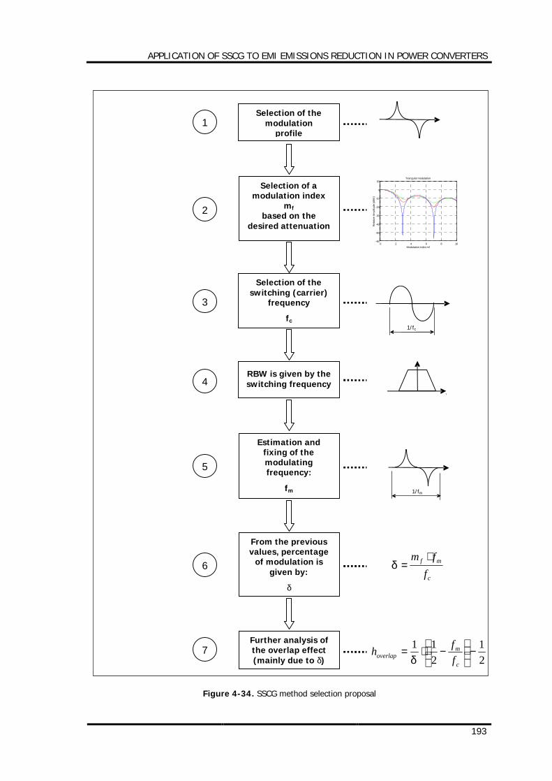
APPLICATION OF SSCG TO EMI EMISSIONS REDUCTION IN POWER CONVERTERS
193
Figure 4-34. SSCG method selection proposal
Selection of the modulation
profile
RBW is given by the switching frequency
Estimation and fixing of the modulating frequency:
fm
Selection of a modulation index
mf based on the
desired attenuation
Selection of the switching (carrier)
frequency
fc
From the previous values, percentage
of modulation is given by:
δ
Further analysis of the overlap effect (mainly due to δ)
0 2 4 6 8 10-60
-50
-40
-30
-20
-10
0
10
Modulation index mf
Rel
ativ
e A
mpl
itude
(dB
V)
Triangular modulation
1/fm
1/fc
c
mf
ffm ⋅
=δ
1
2
3
4
5
6
7 21
211
−
−⋅=
c
moverlap f
fhδ
f

APPLICATION OF SSCG TO EMI EMISSIONS REDUCTION IN POWER CONVERTERS
194
Usually, the first harmonics of the non-modulated switching signal stay inside the
band A (depending on the carrier frequency) thus allowing a 200Hz-RBW setup in
the spectrum analyzer; beyond an usually low harmonic order, signal spectra is
staying inside the band B, this meaning a wider normative RBW of 9 kHz. For
instance, a switching frequency of 120 kHz has its first harmonic inside the band A
and the rest ones (up to 30 MHz) inside the band B, then a change of the RBW
beyond 150 kHz is to be done.
As exposed in clause 4.2, Spectrum Analyzer's RBW affects seriously the practical
measurements and, depending on the case, making the SSCG method produce
negligible or even worse results as theoretically expected. This way, a SSCG method
can be worthy to be implemented for RBW = 200 Hz but less (or even not) worthy
for RBW = 9 kHz (please note that all side-harmonics falling inside the RBW are to
be added arithmetically, thus giving a larger value than expected). In other words,
for a given carrier frequency, it is possible to have a valuable SSCG method for the
first harmonics (because the use of a 200Hz-RBW) but not worthy for the rest of
harmonics because a 9KHz-RBW must be used in the Spectrum Analyzer. All these
comments are referred to situations where a normative measurement is of interest.
Considering the equation 4-28 and the two RBWs under study, in order to obtain
valuable attenuation benefits for harmonic orders inside the band B (150 kHz – 30
MHz) with a 9kHz-RBW, the following expression must be accomplished:
f
kHzm mh
RBWf⋅+
⋅≥1
2 9 (4 -29)
Equally, only attenuation benefits for harmonics inside the band A (9 kHz-150 kHz)
are to be obtained if the following expression is met (where only the first harmonic
is considered) when using a 200Hz-RBW:
f
Hzm m
RBWf+
⋅≥1
2 200 (4 -30)
In order to use the same modulating frequency fm for both bands A & B when using
two different RBWs, the following expression can be applied:
f
kHz
f
Hz
mhRBW
mRBW
⋅+=
+ 119200 (4-31)
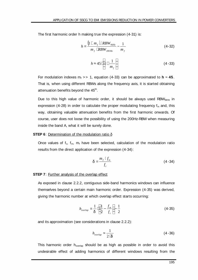
APPLICATION OF SSCG TO EMI EMISSIONS REDUCTION IN POWER CONVERTERS
195
The first harmonic order h making true the expression (4-31) is:
( )fHzf
kHzf
mRBWmRBWm
h 11
200
9 −⋅
⋅+= (4-32)
+⋅≈
fmh 1145 (4 -33)
For modulation indexes mf >> 1, equation (4-33) can be approximated to h ≈ 45.
That is, when using different RBWs along the frequency axis, it is started obtaining
attenuation benefits beyond the 45th.
Due to this high value of harmonic order, it should be always used RBW9kHz in
expression (4-28) in order to calculate the proper modulating frequency fm and, this
way, obtaining valuable attenuation benefits from the first harmonic onwards. Of
course, user does not loose the possibility of using the 200Hz-RBW when measuring
inside the band A, what it will be surely done.
STEP 6: Determination of the modulation ratio δ
Once values of fc, fm, mf have been selected, calculation of the modulation ratio
results from the direct application of the expression (4-34):
c
mf
ffm ⋅
=δ (4 -34)
STEP 7: Further analysis of the overlap effect
As exposed in clause 2.2.2, contiguous side-band harmonics windows can influence
themselves beyond a certain main harmonic order. Expression (4-35) was derived,
giving the harmonic number at which overlap effect starts occurring:
21
211
−
−⋅=
c
moverlap f
fh
δ (4-35)
and its approximation (see considerations in clause 2.2.2):
δ⋅≈
21
overlaph (4 -36)
This harmonic order hoverlap should be as high as possible in order to avoid this
undesirable effect of adding harmonics of different windows resulting from the
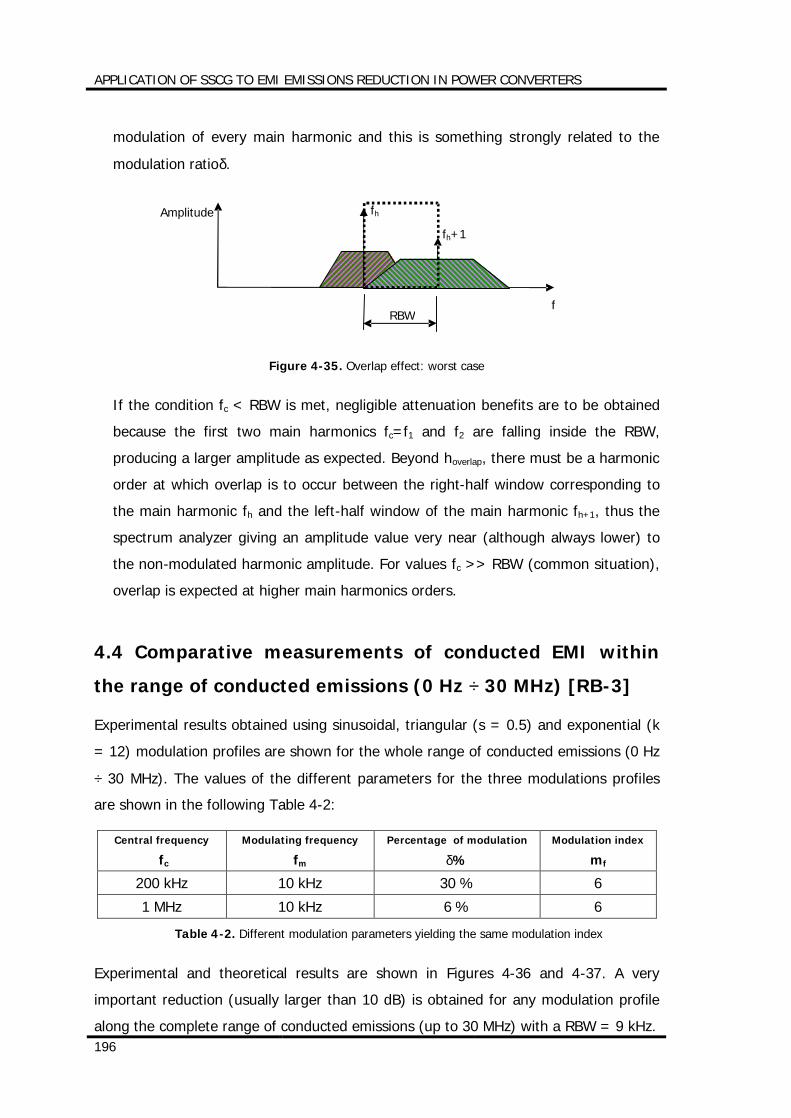
APPLICATION OF SSCG TO EMI EMISSIONS REDUCTION IN POWER CONVERTERS
196
modulation of every main harmonic and this is something strongly related to the
modulation ratioδ.
Figure 4-35. Overlap effect: worst case
If the condition fc < RBW is met, negligible attenuation benefits are to be obtained
because the first two main harmonics fc=f1 and f2 are falling inside the RBW,
producing a larger amplitude as expected. Beyond hoverlap, there must be a harmonic
order at which overlap is to occur between the right-half window corresponding to
the main harmonic fh and the left-half window of the main harmonic fh+1, thus the
spectrum analyzer giving an amplitude value very near (although always lower) to
the non-modulated harmonic amplitude. For values fc >> RBW (common situation),
overlap is expected at higher main harmonics orders.
4.4 Comparative measurements of conducted EMI within
the range of conducted emissions (0 Hz ÷ 30 MHz) [RB-3]
Experimental results obtained using sinusoidal, triangular (s = 0.5) and exponential (k
= 12) modulation profiles are shown for the whole range of conducted emissions (0 Hz
÷ 30 MHz). The values of the different parameters for the three modulations profiles
are shown in the following Table 4-2:
Central frequency
fc Modulating frequency
fm Percentage of modulation
δ% Modulation index
mf
200 kHz 10 kHz 30 % 6
1 MHz 10 kHz 6 % 6
Table 4-2. Different modulation parameters yielding the same modulation index
Experimental and theoretical results are shown in Figures 4-36 and 4-37. A very
important reduction (usually larger than 10 dB) is obtained for any modulation profile
along the complete range of conducted emissions (up to 30 MHz) with a RBW = 9 kHz.
RBW f
Amplitude fh
fh+1
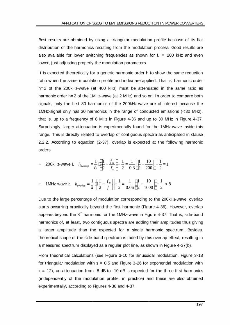
APPLICATION OF SSCG TO EMI EMISSIONS REDUCTION IN POWER CONVERTERS
197
Best results are obtained by using a triangular modulation profile because of its flat
distribution of the harmonics resulting from the modulation process. Good results are
also available for lower switching frequencies as shown for fc = 200 kHz and even
lower, just adjusting properly the modulation parameters.
It is expected theoretically for a generic harmonic order h to show the same reduction
ratio when the same modulation profile and index are applied. That is, harmonic order
h=2 of the 200kHz-wave (at 400 kHz) must be attenuated in the same ratio as
harmonic order h=2 of the 1MHz-wave (at 2 MHz) and so on. In order to compare both
signals, only the first 30 harmonics of the 200kHz-wave are of interest because the
1MHz-signal only has 30 harmonics in the range of conducted emissions (<30 MHz),
that is, up to a frequency of 6 MHz in Figure 4-36 and up to 30 MHz in Figure 4-37.
Surprisingly, larger attenuation is experimentally found for the 1MHz-wave inside this
range. This is directly related to overlap of contiguous spectra as anticipated in clause
2.2.2. According to equation (2-37), overlap is expected at the following harmonic
orders:
− 200kHz-wave è 121
20010
21
3.01
21
211
=−
−=−
−⋅=
c
moverlap f
fh
δ
− 1MHz-wave è 21
100010
21
06.01
21
211
−
−=−
−⋅=
c
moverlap f
fh
δ ≈ 8
Due to the large percentage of modulation corresponding to the 200kHz-wave, overlap
starts occurring practically beyond the first harmonic (Figure 4-36). However, overlap
appears beyond the 8th harmonic for the 1MHz-wave in Figure 4-37. That is, side-band
harmonics of, at least, two contiguous spectra are adding their amplitudes thus giving
a larger amplitude than the expected for a single harmonic spectrum. Besides,
theoretical shape of the side-band spectrum is faded by this overlap effect, resulting in
a measured spectrum displayed as a regular plot line, as shown in Figure 4-37(b).
From theoretical calculations (see Figure 3-10 for sinusoidal modulation, Figure 3-18
for triangular modulation with s = 0.5 and Figure 3-26 for exponential modulation with
k = 12), an attenuation from -8 dB to -10 dB is expected for the three first harmonics
(independently of the modulation profile, in practice) and these are also obtained
experimentally, according to Figures 4-36 and 4-37.
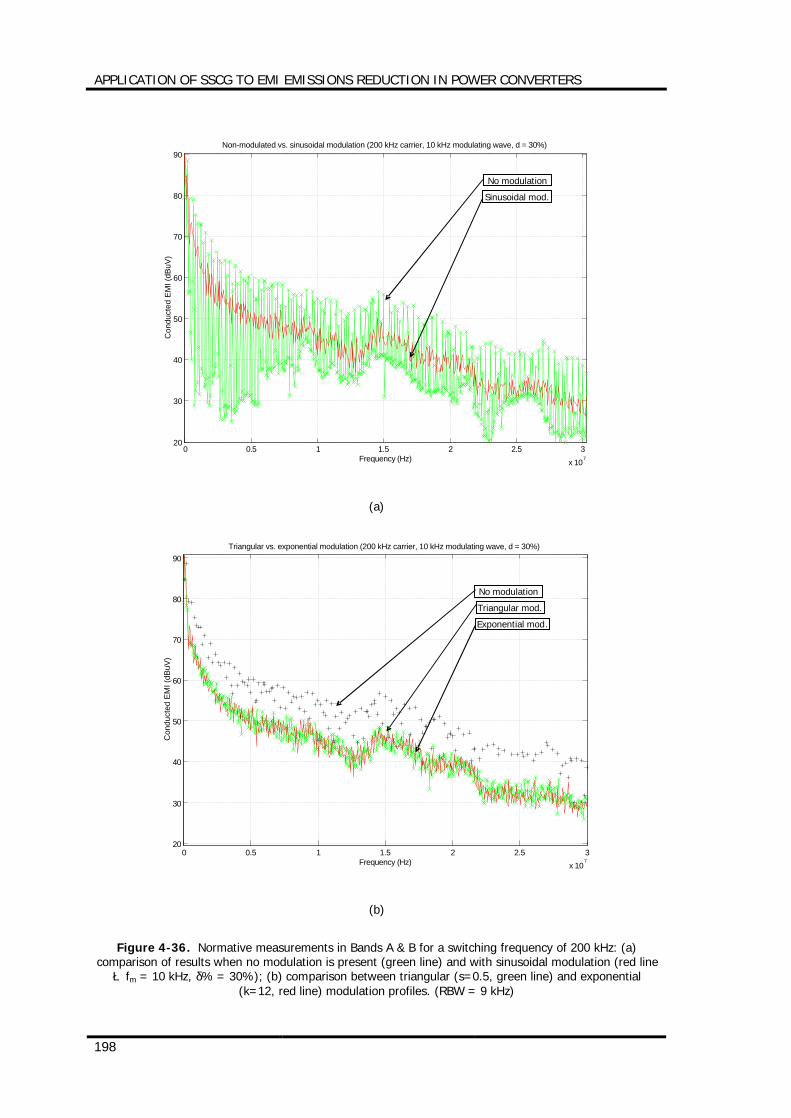
APPLICATION OF SSCG TO EMI EMISSIONS REDUCTION IN POWER CONVERTERS
198
0 0.5 1 1.5 2 2.5 3
x 107
20
30
40
50
60
70
80
90
Frequency (Hz)
Con
duct
ed E
MI (
dBuV
)
Non-modulated vs. sinusoidal modulation (200 kHz carrier, 10 kHz modulating wave, d = 30%)
(a)
0 0.5 1 1.5 2 2.5 3x 10
7
20
30
40
50
60
70
80
90
Frequency (Hz)
Con
duct
ed E
MI (
dBuV
)
Triangular vs. exponential modulation (200 kHz carrier, 10 kHz modulating wave, d = 30%)
(b)
Figure 4-36. Normative measurements in Bands A & B for a switching frequency of 200 kHz: (a) comparison of results when no modulation is present (green line) and with sinusoidal modulation (red line èfm = 10 kHz, δ% = 30%); (b) comparison between triangular (s=0.5, green line) and exponential
(k=12, red line) modulation profiles. (RBW = 9 kHz)
No modulation
Sinusoidal mod.
Triangular mod.
Exponential mod.
No modulation
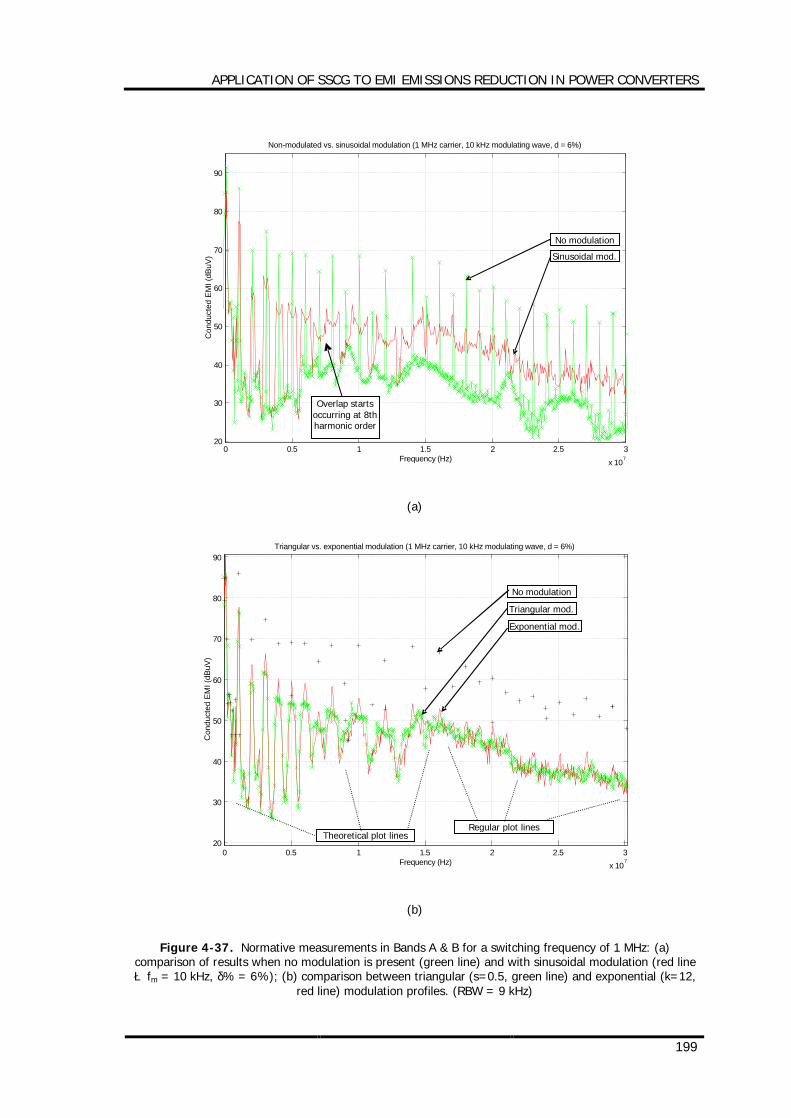
APPLICATION OF SSCG TO EMI EMISSIONS REDUCTION IN POWER CONVERTERS
199
0 0.5 1 1.5 2 2.5 3
x 107
20
30
40
50
60
70
80
90
Frequency (Hz)
Con
duct
ed E
MI (
dBuV
)
Non-modulated vs. sinusoidal modulation (1 MHz carrier, 10 kHz modulating wave, d = 6%)
(a)
0 0.5 1 1.5 2 2.5 3x 10
7
20
30
40
50
60
70
80
90
Frequency (Hz)
Con
duct
ed E
MI (
dBuV
)
Triangular vs. exponential modulation (1 MHz carrier, 10 kHz modulating wave, d = 6%)
(b)
Figure 4-37. Normative measurements in Bands A & B for a switching frequency of 1 MHz: (a) comparison of results when no modulation is present (green line) and with sinusoidal modulation (red line èfm = 10 kHz, δ% = 6%); (b) comparison between triangular (s=0.5, green line) and exponential (k=12,
red line) modulation profiles. (RBW = 9 kHz)
No modulation
Sinusoidal mod.
Triangular mod.
Exponential mod.
No modulation
Regular plot lines Theoretical plot lines
Overlap starts occurring at 8th harmonic order
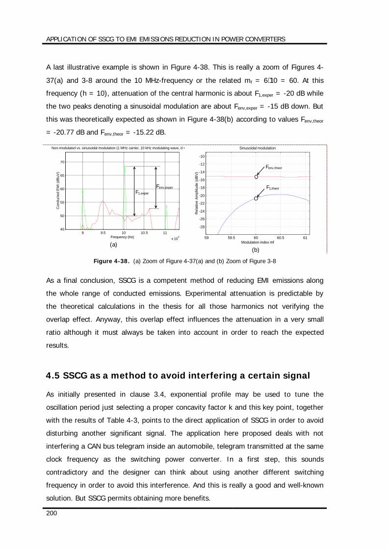
APPLICATION OF SSCG TO EMI EMISSIONS REDUCTION IN POWER CONVERTERS
200
A last illustrative example is shown in Figure 4-38. This is really a zoom of Figures 4-
37(a) and 3-8 around the 10 MHz-frequency or the related mf = 6⋅10 = 60. At this
frequency (h = 10), attenuation of the central harmonic is about F1,exper = -20 dB while
the two peaks denoting a sinusoidal modulation are about Fenv,exper = -15 dB down. But
this was theoretically expected as shown in Figure 4-38(b) according to values Fenv,theor
= -20.77 dB and Fenv,theor = -15.22 dB.
9 9.5 10 10.5 11x 106
45
50
55
60
65
70
Frequency (Hz)
Con
duct
ed E
MI (
dBuV
)
Non-modulated vs. sinusoidal modulation (1 MHz carrier, 10 kHz modulating wave, d = 6%)
(a) 59 59.5 60 60.5 61
-28
-26
-24
-22
-20
-18
-16
-14
-12
-10
Modulation index mf
Rel
ativ
e Am
plitu
de (d
BV)
Sinusoidal modulation
(b)
Figure 4-38. (a) Zoom of Figure 4-37(a) and (b) Zoom of Figure 3-8
As a final conclusion, SSCG is a competent method of reducing EMI emissions along
the whole range of conducted emissions. Experimental attenuation is predictable by
the theoretical calculations in the thesis for all those harmonics not verifying the
overlap effect. Anyway, this overlap effect influences the attenuation in a very small
ratio although it must always be taken into account in order to reach the expected
results.
4.5 SSCG as a method to avoid interfering a certain signal
As initially presented in clause 3.4, exponential profile may be used to tune the
oscillation period just selecting a proper concavity factor k and this key point, together
with the results of Table 4-3, points to the direct application of SSCG in order to avoid
disturbing another significant signal. The application here proposed deals with not
interfering a CAN bus telegram inside an automobile, telegram transmitted at the same
clock frequency as the switching power converter. In a first step, this sounds
contradictory and the designer can think about using another different switching
frequency in order to avoid this interference. And this is really a good and well-known
solution. But SSCG permits obtaining more benefits.
F1,exper Fenv,exper
Fenv,theor
F1,theor
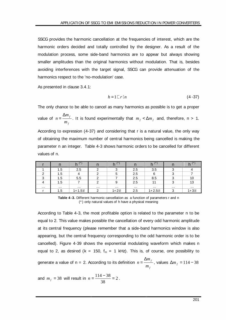
APPLICATION OF SSCG TO EMI EMISSIONS REDUCTION IN POWER CONVERTERS
201
SSCG provides the harmonic cancellation at the frequencies of interest, which are the
harmonic orders decided and totally controlled by the designer. As a result of the
modulation process, some side-band harmonics are to appear but always showing
smaller amplitudes than the original harmonics without modulation. That is, besides
avoiding interferences with the target signal, SSCG can provide attenuation of the
harmonics respect to the 'no-modulation' case.
As presented in clause 3.4.1:
nrh ⋅+=1 (4 -37)
The only chance to be able to cancel as many harmonics as possible is to get a proper
value of f
f
mm
n∆
= . It is found experimentally that ff mm ∆< and, therefore, n > 1.
According to expression (4-37) and considering that r is a natural value, the only way
of obtaining the maximum number of central harmonics being cancelled is making the
parameter n an integer. Table 4-3 shows harmonic orders to be cancelled for different
values of n.
r n h (*) n h (*) n h (*) n h (*) 1 1.5 2.5 2 3 2.5 3.5 3 4 2 1.5 4 2 5 2.5 6 3 7 3 1.5 5.5 2 7 2.5 8.5 3 10 4 1.5 7 2 9 2.5 11 3 13 … … … … … … … … … r 1.5 1+1.5⋅r 2 1+2⋅r 2.5 1+2.5⋅r 3 1+3⋅r
Table 4-3. Different harmonic cancellation as a function of parameters r and n (*) only natural values of h have a physical meaning
According to Table 4-3, the most profitable option is related to the parameter n to be
equal to 2. This value makes possible the cancellation of every odd harmonic amplitude
at its central frequency (please remember that a side-band harmonics window is also
appearing, but the central frequency corresponding to the odd harmonic order is to be
cancelled). Figure 4-39 shows the exponential modulating waveform which makes n
equal to 2, as desired (k = 150, fm = 1 kHz). This is, of course, one possibility to
generate a value of n = 2. According to its definition f
f
mm
n∆
= , values 38114 −=∆ fm
and 38=fm will result in 238
38114=
−=n .
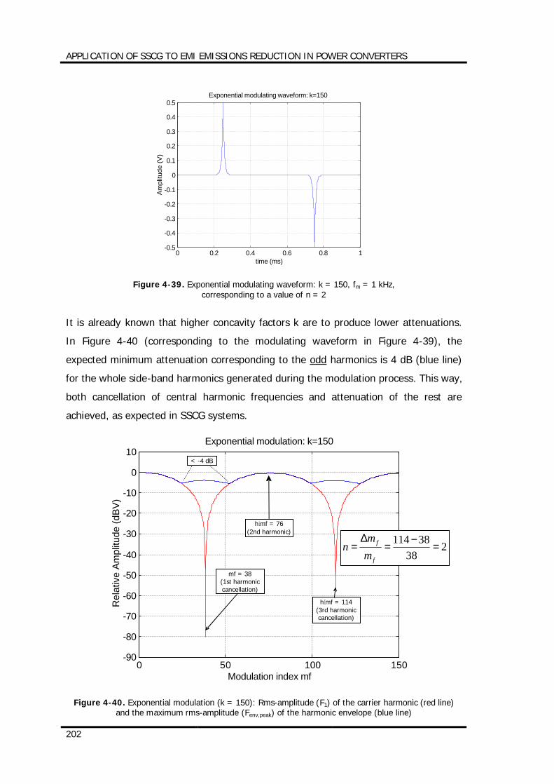
APPLICATION OF SSCG TO EMI EMISSIONS REDUCTION IN POWER CONVERTERS
202
0 0.2 0.4 0.6 0.8 1
-0.5
-0.4
-0.3
-0.2
-0.1
0
0.1
0.2
0.3
0.4
0.5
time (ms)
Ampl
itude
(V)
Exponential modulating waveform: k=150
Figure 4-39. Exponential modulating waveform: k = 150, fm = 1 kHz, corresponding to a value of n = 2
It is already known that higher concavity factors k are to produce lower attenuations.
In Figure 4-40 (corresponding to the modulating waveform in Figure 4-39), the
expected minimum attenuation corresponding to the odd harmonics is 4 dB (blue line)
for the whole side-band harmonics generated during the modulation process. This way,
both cancellation of central harmonic frequencies and attenuation of the rest are
achieved, as expected in SSCG systems.
0 50 100 150-90
-80
-70
-60
-50
-40
-30
-20
-10
0
10
Modulation index mf
Rel
ativ
e Am
plitu
de (d
BV)
Exponential modulation: k=150
Figure 4-40. Exponential modulation (k = 150): Rms-amplitude (F1) of the carrier harmonic (red line) and the maximum rms-amplitude (Fenv,peak) of the harmonic envelope (blue line)
mf = 38 (1st harmonic cancellation)
h⋅mf = 114 (3rd harmonic cancellation)
238
38114=
−=
∆=
f
f
mm
n
< -4 dB
h⋅mf = 76 (2nd harmonic)
APPLICATION OF SSCG TO EMI EMISSIONS REDUCTION IN POWER CONVERTERS
203
The target signal to be preserved completely is, for instance, a CAN message at high
speed (500 kHz) [RD-7]. This is a trapezoidal signal of nominal duty-cycle D = 50%.
Because of that, only odd harmonics are expected; this way, preventing the CAN-
system from external interferences at these odd harmonic frequencies, no distortion or
undesired coupling is to happen. This is the intention of the following experiment.
Assuming a power converter working at the same frequency as the CAN-system (fc =
500 kHz), a proper modulation process will allow the power converter to cancel its
harmonic amplitudes at the frequencies being equal to the harmonics of the CAN
signal.
Next plots in Figures 4-41 and 4-43 show the experimental measurements when the
power converter switching frequency of the test plant was modulated by an
exponential profile with the following parameters:
• Modulation index mf = 38 (according to the results in Figure 4-40)
• Concavity factor k = 150
• Modulating frequency fm = 1 kHz
• Switching frequency fc = 500 kHz
• Percentage of modulation 100⋅⋅
=c
fm
fmf
δ =7.6 %
The first six odd-harmonics at multiples of the switching frequency (500 kHz) are
displayed in Figure 4-41. A strong attenuation is observed at these odd-harmonic
orders by means of the exponential modulation under test. Besides, the largest side-
band harmonics resulting from the modulation process are ≈4 dB smaller (in average)
than the original harmonics, that is, when no modulation is present, as expected
theoretically (see previous comments).
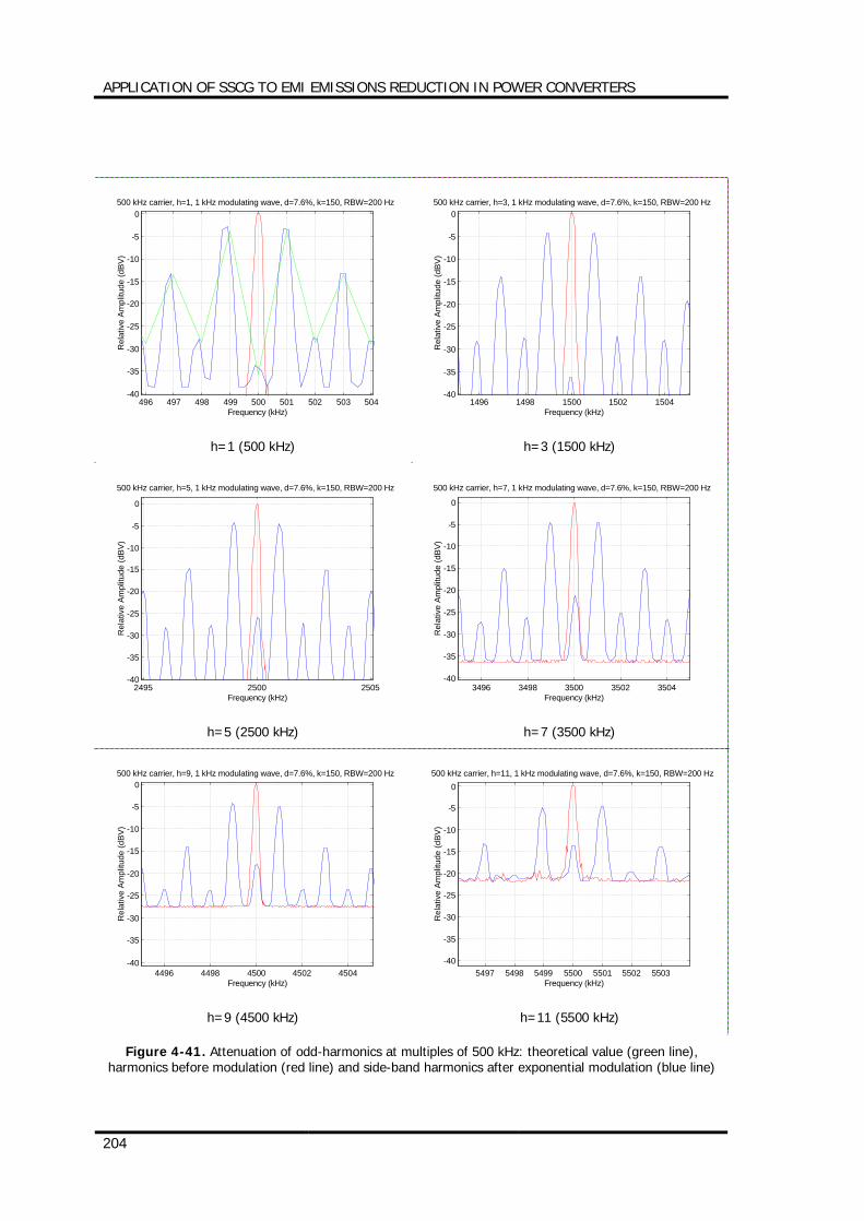
APPLICATION OF SSCG TO EMI EMISSIONS REDUCTION IN POWER CONVERTERS
204
496 497 498 499 500 501 502 503 504-40
-35
-30
-25
-20
-15
-10
-5
0
Frequency (kHz)
Rel
ativ
e Am
plitu
de (d
BV)
500 kHz carrier, h=1, 1 kHz modulating wave, d=7.6%, k=150, RBW=200 Hz
h=1 (500 kHz)
1496 1498 1500 1502 1504-40
-35
-30
-25
-20
-15
-10
-5
0
Frequency (kHz)
Rel
ativ
e Am
plitu
de (d
BV)
500 kHz carrier, h=3, 1 kHz modulating wave, d=7.6%, k=150, RBW=200 Hz
h=3 (1500 kHz)
2495 2500 2505-40
-35
-30
-25
-20
-15
-10
-5
0
Frequency (kHz)
Rel
ativ
e Am
plitu
de (d
BV)
500 kHz carrier, h=5, 1 kHz modulating wave, d=7.6%, k=150, RBW=200 Hz
h=5 (2500 kHz)
3496 3498 3500 3502 3504-40
-35
-30
-25
-20
-15
-10
-5
0
Frequency (kHz)
Rel
ativ
e Am
plitu
de (d
BV)
500 kHz carrier, h=7, 1 kHz modulating wave, d=7.6%, k=150, RBW=200 Hz
h=7 (3500 kHz)
4496 4498 4500 4502 4504-40
-35
-30
-25
-20
-15
-10
-5
0
Frequency (kHz)
Rel
ativ
e Am
plitu
de (d
BV)
500 kHz carrier, h=9, 1 kHz modulating wave, d=7.6%, k=150, RBW=200 Hz
h=9 (4500 kHz)
5497 5498 5499 5500 5501 5502 5503-40
-35
-30
-25
-20
-15
-10
-5
0
Frequency (kHz)
Rel
ativ
e Am
plitu
de (d
BV)
500 kHz carrier, h=11, 1 kHz modulating wave, d=7.6%, k=150, RBW=200 Hz
h=11 (5500 kHz)
Figure 4-41. Attenuation of odd-harmonics at multiples of 500 kHz: theoretical value (green line), harmonics before modulation (red line) and side-band harmonics after exponential modulation (blue line)
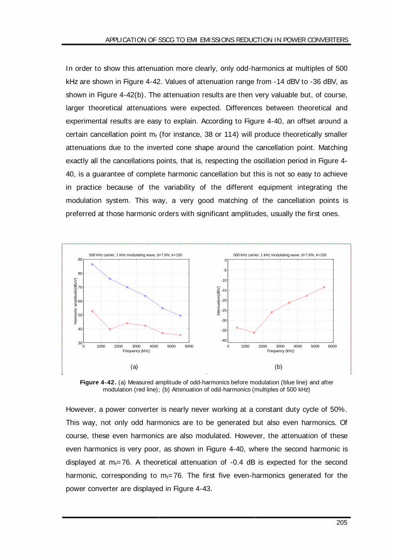
APPLICATION OF SSCG TO EMI EMISSIONS REDUCTION IN POWER CONVERTERS
205
In order to show this attenuation more clearly, only odd-harmonics at multiples of 500
kHz are shown in Figure 4-42. Values of attenuation range from -14 dBV to -36 dBV, as
shown in Figure 4-42(b). The attenuation results are then very valuable but, of course,
larger theoretical attenuations were expected. Differences between theoretical and
experimental results are easy to explain. According to Figure 4-40, an offset around a
certain cancellation point mf (for instance, 38 or 114) will produce theoretically smaller
attenuations due to the inverted cone shape around the cancellation point. Matching
exactly all the cancellations points, that is, respecting the oscillation period in Figure 4-
40, is a guarantee of complete harmonic cancellation but this is not so easy to achieve
in practice because of the variability of the different equipment integrating the
modulation system. This way, a very good matching of the cancellation points is
preferred at those harmonic orders with significant amplitudes, usually the first ones.
0 1000 2000 3000 4000 5000 600030
40
50
60
70
80
90
Frequency (kHz)
Har
mon
ic a
mpl
itude
(dBu
V)
500 kHz carrier, 1 kHz modulating wave, d=7.6%, k=150
(a)
0 1000 2000 3000 4000 5000 6000-40
-35
-30
-25
-20
-15
-10
-5
0
Frequency (kHz)
Atte
nuat
ion(
dBV)
500 kHz carrier, 1 kHz modulating wave, d=7.6%, k=150
(b)
Figure 4-42. (a) Measured amplitude of odd-harmonics before modulation (blue line) and after modulation (red line); (b) Attenuation of odd-harmonics (multiples of 500 kHz)
However, a power converter is nearly never working at a constant duty cycle of 50%.
This way, not only odd harmonics are to be generated but also even harmonics. Of
course, these even harmonics are also modulated. However, the attenuation of these
even harmonics is very poor, as shown in Figure 4-40, where the second harmonic is
displayed at mf=76. A theoretical attenuation of -0.4 dB is expected for the second
harmonic, corresponding to mf=76. The first five even-harmonics generated for the
power converter are displayed in Figure 4-43.
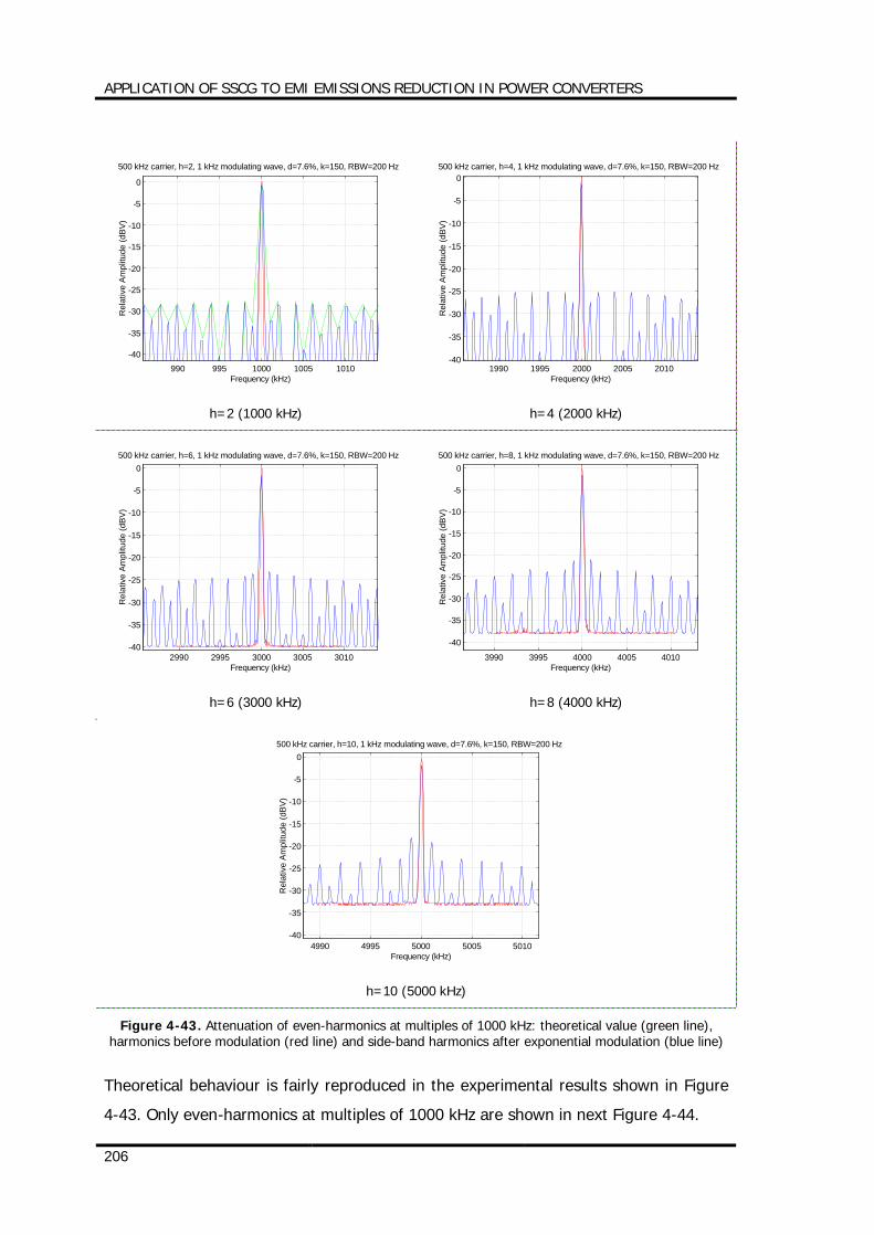
APPLICATION OF SSCG TO EMI EMISSIONS REDUCTION IN POWER CONVERTERS
206
990 995 1000 1005 1010-40
-35
-30
-25
-20
-15
-10
-5
0
Frequency (kHz)
Rel
ativ
e Am
plitu
de (d
BV)
500 kHz carrier, h=2, 1 kHz modulating wave, d=7.6%, k=150, RBW=200 Hz
h=2 (1000 kHz)
1990 1995 2000 2005 2010-40
-35
-30
-25
-20
-15
-10
-5
0
Frequency (kHz)
Rel
ativ
e Am
plitu
de (d
BV)
500 kHz carrier, h=4, 1 kHz modulating wave, d=7.6%, k=150, RBW=200 Hz
h=4 (2000 kHz)
2990 2995 3000 3005 3010-40
-35
-30
-25
-20
-15
-10
-5
0
Frequency (kHz)
Rel
ativ
e Am
plitu
de (d
BV)
500 kHz carrier, h=6, 1 kHz modulating wave, d=7.6%, k=150, RBW=200 Hz
h=6 (3000 kHz)
3990 3995 4000 4005 4010
-40
-35
-30
-25
-20
-15
-10
-5
0
Frequency (kHz)
Rel
ativ
e Am
plitu
de (d
BV)
500 kHz carrier, h=8, 1 kHz modulating wave, d=7.6%, k=150, RBW=200 Hz
h=8 (4000 kHz)
4990 4995 5000 5005 5010-40
-35
-30
-25
-20
-15
-10
-5
0
Frequency (kHz)
Rel
ativ
e Am
plitu
de (d
BV)
500 kHz carrier, h=10, 1 kHz modulating wave, d=7.6%, k=150, RBW=200 Hz
h=10 (5000 kHz)
Figure 4-43. Attenuation of even-harmonics at multiples of 1000 kHz: theoretical value (green line), harmonics before modulation (red line) and side-band harmonics after exponential modulation (blue line)
Theoretical behaviour is fairly reproduced in the experimental results shown in Figure
4-43. Only even-harmonics at multiples of 1000 kHz are shown in next Figure 4-44.
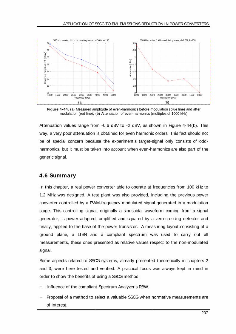
APPLICATION OF SSCG TO EMI EMISSIONS REDUCTION IN POWER CONVERTERS
207
1000 1500 2000 2500 3000 3500 4000 4500 500058
60
62
64
66
68
70
72
Frequency (kHz)
Har
mon
ic a
mpl
itude
F1
(dBu
V)
500 kHz carrier, 1 kHz modulating wave, d=7.6%, k=150
(a)
1000 1500 2000 2500 3000 3500 4000 4500 5000-2
-1.8
-1.6
-1.4
-1.2
-1
-0.8
-0.6
Frequency (kHz)
Atte
nuat
ion(
dBV)
500 kHz carrier, 1 kHz modulating wave, d=7.6%, k=150
(b)
Figure 4-44. (a) Measured amplitude of even-harmonics before modulation (blue line) and after modulation (red line); (b) Attenuation of even-harmonics (multiples of 1000 kHz)
Attenuation values range from -0.6 dBV to -2 dBV, as shown in Figure 4-44(b). This
way, a very poor attenuation is obtained for even harmonic orders. This fact should not
be of special concern because the experiment's target-signal only consists of odd-
harmonics, but it must be taken into account when even-harmonics are also part of the
generic signal.
4.6 Summary
In this chapter, a real power converter able to operate at frequencies from 100 kHz to
1.2 MHz was designed. A test plant was also provided, including the previous power
converter controlled by a PWM-frequency modulated signal generated in a modulation
stage. This controlling signal, originally a sinusoidal waveform coming from a signal
generator, is power-adapted, amplified and squared by a zero-crossing detector and
finally, applied to the base of the power transistor. A measuring layout consisting of a
ground plane, a LISN and a compliant spectrum was used to carry out all
measurements, these ones presented as relative values respect to the non-modulated
signal.
Some aspects related to SSCG systems, already presented theoretically in chapters 2
and 3, were here tested and verified. A practical focus was always kept in mind in
order to show the benefits of using a SSCG method:
− Influence of the compliant Spectrum Analyzer's RBW.
− Proposal of a method to select a valuable SSCG when normative measurements are
of interest.
APPLICATION OF SSCG TO EMI EMISSIONS REDUCTION IN POWER CONVERTERS
208
− Conducted EMI (0÷30 MHz) with and without SSGC modulations.
− SSCG as a method to avoid interferences with a certain signal.
As explained along the thesis, real EMI attenuation benefits are always obtained. This
true reduction capability can be faded by normative considerations, mainly related to
the regulatory RBW to be set on the compliant Spectrum Analyzer. Only when
normative measurements are of interest, a special care must be taken to select a
proper SSCG method in order to maintain these EMI attenuation benefits when
measuring.
Experimental results in clause 4.2 show that modulating frequencies verifying the
condition f
m mRBWf+
>1
2 (where RBW is the Resolution Bandwidth and mf, the
modulation index) start producing worthy measurements, not being necessary to reach
the condition RBW < fm to achieve a useful measured attenuation. With this new
condition and the previous experimental results, a guideline to select a valuable SSCG
method is offered in clause 4.3, consisting of 7 steps. Each step deals with a different
parameter of a SSCG method, being a summary of all previous results obtained along
the thesis.
In order to assess the validity of using a SSCG method along the range of conducted
emissions (0÷30 MHz), a practical example of SSCG modulation is presented in clause
4.4. Attenuation results are shown for the three modulation profiles under study
(sinusoidal, triangular and exponential) and for two different sets of modulation
parameters. It is observed some undesired effects like side-band spectra overlap and,
therefore, lower attenuation than expected at higher frequencies but it is clearly
evidenced an attenuation higher than 10 dB for every modulation profile along the
whole range of conducted emissions, what allows to assure that SSCG is a worthy
method to reduce EMI emissions coming from switching power converters.
Finally, a special application of SSCG techniques is presented in clause 4.5 related to
the ability of frequency modulation to cancel harmonics at certain frequencies. Practical
application deals with the possibility of having two systems sharing the same
frequency. The systems here presented are a CAN-system at high speed (500 kHz) and
a power converter operated at 500 kHz. In order to avoid any interferences from the
power converter to the CAN-system, a SSCG modulation is implemented in the
APPLICATION OF SSCG TO EMI EMISSIONS REDUCTION IN POWER CONVERTERS
209
switching power converter in such a way that harmonics at multiples of 500 kHz
coming from the power converter are cancelled in practice; this way, no interference is
expected in the CAN-system even when both systems are working nominally at the
same frequency.


C H A P T E R
5
CONCLUSIONS

CONCLUSIONS
213
5. CONCLUSIONS
EMI attenuation benefits of SSCG are well-known, mainly applied to systems with
higher frequency signals such as clock lines and clock-related waveforms (port lines,
serial communications and so on). Presence of SSCG-techniques in digital systems is
not strange in some commercial applications (mainly, in personal computers and
microcontrollers) but it is nearly unknown in the world of switching power converters,
characterised by lower frequency signals. A first question was related to the worthy
possibility of implementing such techniques in switching power converters in order to
reduce EMI emissions produced by the PWM signal controlling these converters or,
even more, avoid undesired interferences with other systems working at the same
nominal frequency. Anyway, before facing this task, it is useful (when not mandatory)
to describe and systematize theoretically the behaviour of these special kind of
frequency modulation called SSCG. Although theoretical development only considers
the modulation of a sinusoidal waveform (for convenience), it is demonstrated the
validity of all results when a generic signal is present, just paying attention to the right
use of the harmonic order h in every expression derived for the modulation of a
sinusoidal waveform. Square waves, common in power converters, can be split up in a
series of sinusoidal waves (fundamental + harmonics è Fourier series). The benefits
of SSCG on a sinus wave are observed in each harmonic, so it is worthy to make the
theoretical study on a sinusoidal carrier. Some conclusions are extracted from this
theoretical analysis:
− After modulation, a single harmonic changes into an amount of side-band
harmonics with amplitudes smaller than the non-modulated harmonic and
separated by a frequency fm (modulating frequency). Amplitudes of side-band
harmonics resulting from modulation show a different aspect or outline depending
on the modulation profile. For a sinusoidal modulation profile, side-band harmonics
tend to concentrate themselves around the two peaks defining the side-band
harmonics bandwidth as the modulation index mf gets higher. This results in a
shape of the modulation spectrum envelope showing two peaks at both ends of the
bandwidth while the envelope gets a larger concavity between these two peaks. In
the case of a triangular modulation profile, envelope of the side-band harmonics
corresponds to a nearly flat, straight horizontal line (with harmonic amplitudes
CONCLUSIONS
214
concentrated in a narrow range of variation for vertex index s ≠ 0.5) , very
opposite to the sinusoidal modulation behaviour, characterised by a concavity
between two extreme peaks and to the case of an exponential modulation profile,
where side-band harmonics resulting from the modulation process tend to
concentrate around the carrier frequency, decreasing in amplitude as the side-band
harmonic order separates itself from the carrier frequency.
− As just said, a triangular modulation produces a flat side-band harmonics spectrum.
Considering a triangular profile as the reference base, profiles plotted outside the
triangular profile limits (e.g., sinusoidal) seems to concentrate harmonics around
the two peaks defining the bandwidth; in the same way, profiles plotted inside the
reference triangular profile (e.g., exponential) concentrate harmonics around the
carrier frequency. A combination of these three cases in a generic modulation
profile allows the designer to generate whichever shape of the side-band
harmonics spectrum.
− For every modulation profile, amplitude reduction of the side-band harmonics
resulting from the modulation process only depends on the modulation index mf.
This way, a graphical representation of attenuation versus modulation index is
presented as theoretical results. Values of attenuation are referred as relative
amplitudes before and after modulation.
− Some parameters were defined in order to quantify the attenuation characteristics:
F1 is the RMS-amplitude of the harmonic corresponding to the modulated waveform
at the carrier (switching) frequency fc; Fenv,peak is the maximum RMS-amplitude of
the side-band harmonic envelope corresponding to the modulated waveform: it
provides a very useful information because all side-band harmonics amplitudes will
be under this value Fenv,peak; ∆fpeak is the distance in frequency between the two
envelope peaks of value Fenv,peak.
− Regarding the evolution of amplitude F1, the following considerations for the three
profiles under study are of interest:
§ Representing the harmonic amplitude F1 as a function of mf, it is obtained an
attenuation plot whose envelope results in a logarithmical curve. This way, the
higher the modulation index, the larger the attenuation; however, this
conclusion is only valid considering the envelope. For modulation indexes mf <
200, attenuation increases very fast due to its logarithmical behaviour.
CONCLUSIONS
215
Comparing the three profiles under study, a very small difference of 2 dBV
appears at high modulation indexes between sinusoidal and triangular
modulation; this is not the case of the exponential modulation, whose
attenuation is very poor compared to the two previous profiles.
§ Attenuation plots of F1 show oscillations at a constant period of 1.3 (in units of
mf) for sinusoidal modulation, 1.41 for triangular modulation and a value
depending on the concavity factor k for exponential modulation. At every
oscillation along mf -axis, harmonic amplitudes reach a minimum value with
attenuation values higher than 40 dB, that is, it can be said that this harmonic
is cancelled at this particular mf. This way, a special profit can be taken just
tuning the system to a concrete modulation index in order, for instance, to
eliminate the harmonic at the carrier frequency. In the case of exponential
modulation profile, it is possible to let the modulation index fix and tune the
concavity factor k in order to cancel a particular harmonic. In the case of
triangular modulation, no cancellation is possible for vertex index s ≠ 0.5.
− Regarding the evolution of the maximum envelope amplitude Fenv,peak, consider the
following comments for the three profiles under study:
§ Representing the maximum envelope amplitude Fenv,peak as a function of mf, it
is obtained an attenuation plot whose envelope results in a logarithmical
curve. Again, the higher the modulation index, the larger the attenuation, only
valid considering the envelope of Fenv,peak. For modulation indexes of mf < 200,
attenuation increases very fast due to its logarithmical behaviour. Comparing
the three profiles, exponential profile shows the worst behaviour because of
the peak shape of the side-band harmonic distribution, which makes the F1
value matches Fenv,peak most of the time; however, sinusoidal and, in a much
higher quantity, triangular modulations give very good values of attenuation
at any side-band harmonic order.
§ Attenuation plots of Fenv,peak show oscillations much smaller than those
corresponding to F1; because of that, main efforts should be concentrated on
obtaining a cancellation of a certain harmonic, normally, the one at the carrier
frequency.
− Related to the evolution of the peak-to-peak envelope bandwidth ∆fpeak, further
comments are of interest:
CONCLUSIONS
216
§ For sinusoidal modulation, envelope of ∆fpeak shows a linear trend respect to
mf, that is, higher modulation indexes mf are to produce wider bandwidths in
a linear ratio. Zooming the plot of ∆fpeak, it is observed that this parameter
increases in steps of a constant value equal to 2⋅fm.
§ For triangular modulation, maximum values of ∆fpeak show a linear trend
respect to mf . Under this theoretical straight line, a chaotic behaviour is
shown, which is strongly related to the flat shape of the side-band harmonic
spectra distribution. However, both sinusoidal and triangular modulations
(with vertex index s = 0.5) show approximately the same straight line slope (≈
2⋅fm); for vertex indexes s different of 0.5, this slope is smaller in triangular
modulation.
§ For exponential modulation, opposite to the sinusoidal and triangular profiles,
no linear trend is detected, just a chaotic behaviour of ∆fpeak. Moreover, the
maximum bandwidth ∆fpeak is much smaller than for sinusoidal and triangular
cases. This indicates the concentration of harmonics around the carrier
frequency, which is also bigger as the concavity factor k increases.
− From the comparison of the three different modulation profiles under study and
considering the global behaviour of the modulation, the most important parameter
is Fenv,peak because all harmonic amplitudes (resulting from the modulation process)
will be under this value Fenv,peak. If the number of new harmonics generated during
the modulation process is not of concern but only their amplitudes, this parameter
Fenv,peak should be the target. Then, a flat harmonic distribution is the most
profitable and, therefore, a triangular modulation profile is the most suitable for
any application with these characteristics. Exponential profile shows the worst
behaviour because of the peak shape of the side-band harmonic distribution. If
attenuation given by an exponential profile at a certain modulation index mf is
found to be satisfactory, then it can be a good option because the side-band
harmonics decrease fast as the side-harmonic order gets farther from the central
frequency.
Previous comments constitute the answer to one of the thesis's objectives: to have
SSCG-techniques analytically expressed and systematized; this way, this objective is
covered successfully.
CONCLUSIONS
217
Once a detailed theoretical description of the SSCG modulation is available, the second
question (as expressed above) is related to the worthy possibility of implementing such
techniques in switching power converters in order to reduce EMI emissions produced
by the PWM signal controlling these converters or, even more, avoid undesired
interferences with other systems working at the same nominal frequency. This is the
main objective of the thesis and it can be assure that SSCG techniques can be worthy
and successfully implemented in switching power converters in order to cover both
attenuation exigencies.
The key point is to find a proper modulation index mf covering the attenuation
necessities. Previous theoretical aspects facilitate the selection of the proper
modulation index. Because of its definitionm
cf f
fm ⋅=
δ, this is done by selecting
properly the modulation ratio δ, the carrier frequency fc and the modulating frequency
fm. In order to be successful in the selection of these values, some considerations must
be taken into account:
− Carrier (or switching) frequency fc, and modulating frequency fm (defines the
distance in frequency between two consecutive side-band harmonics) are of
interest when measuring with spectrum analyzers: their RBW (Resolution
Bandwidth) and measure mode (peak, quasy-peak and average) are responsible
for giving different measured values of the same physical fact of modulation; as a
general asseveration, the larger the selected RBW, the higher the obtained
measure because more side-band harmonics can fall inside this RBW, adding their
amplitudes. Switching (carrier) frequency in power converters is not usually too
large because the electronics components (diodes and power transistors, mainly)
are not able to manage larger power with shorter switching times. Anyway, use of
higher switching frequencies is advisable in order to reduce the size and power
capability of the passive components (filters, inductances, diodes, transistors and
so on) and increase the power efficiency of the converter (> 70 %).
As the attenuation increases with larger modulation indexes, higher switching
frequencies fc are preferred.
− Modulation index mf (together with fm, defines the bandwidth of the FM
waveform), carrier frequency peak deviation ∆fc (defines the peak frequency
excursion around fc) and modulation ratio δ are responsible for the spectrum
CONCLUSIONS
218
overlap at higher harmonic orders because of the growing side-band harmonics
bandwidth resulting from the modulation process. Parameters fm and ∆fc define the
side-band harmonics bandwidth around the carrier (or switching) frequency, thus
giving the lowest working frequency present in the system (≈fc -∆fc) which must be
higher than the cut-off frequency of the low-pass filter integrated in the power
converter in order to avoid frequencies under cut-off to be present on the output
voltage. As explained along the thesis, real EMI attenuation benefits are always
obtained. This true reduction capability can be faded by normative considerations,
mainly related to the regulatory RBW to be set on the compliant Spectrum
Analyzer. Only when normative measurements are of interest, a special care must
be taken to select a proper SSCG method in order to maintain these EMI
attenuation benefits when measuring. Experimental results show that modulating
frequencies verifying the condition f
m mRBWf+
>1
2 (where RBW is the Resolution
Bandwidth and mf, the modulation index) start producing worthy measurements,
not being necessary to reach the condition RBW < fm to achieve a useful measured
attenuation.
It is commonly worthy to work with higher modulation indexes and, through its
definition m
cf f
fm ⋅=
δ, this can be done by increasing the modulation ratio δ or the
carrier frequency fc or decreasing the modulating frequency fm.
− Related to the previous point, overlap starts at main harmonic order given by the
following expression 21
211
−
−⋅=
c
moverlap f
fh
δ. This overlap is the main reason
for not obtaining the expected attenuation at higher harmonic orders. In order to
assess the validity of using a SSCG techniques along the range of conducted
emissions (0÷30 MHz), a practical example of SSCG modulation was carried out.
Attenuation results were shown for the three modulation profiles under study
(sinusoidal, triangular and exponential) and for two different sets of modulation
parameters. It was observed some undesired effects like side-band spectra overlap
and, therefore, lower attenuation than expected at higher frequencies but it was
clearly evidenced an attenuation higher than 10 dB for every modulation profile
along the whole range of conducted emissions, what allows to assure that SSCG is
CONCLUSIONS
219
a worthy method to reduce EMI emissions coming from switching power
converters.
− Regarding modulation profiles (define the shape of the resulting modulated
waveform spectrum and the possibility of up- and down-spreading SSCG
techniques), it was also demonstrated there was no influence of the modulation
profile on the output voltage of a power converter; a voltage offset in the
modulation profile does not modify the final modulation spectrum but only the
central frequency of the side-band harmonics window, thus being an easy way to
implement up- and down-spreading modulation techniques; in a similar way,
resulting modulated wave spectrum is independent on a possible phase-shift in the
modulation profile. Anyway, modulation profile to be selected is depending on the
systems necessities or exigencies and no generic formula can be given
Finally, SSCG-techniques offer the capability of moving the modulation spectrum as
desired (of course, with certain limitations); this fact can be profitable in order to avoid
undesired interferences with other systems. A special application of SSCG techniques
was presented in order to show the ability of frequency modulation to cancel
harmonics at certain frequencies. Practical application dealt with the possibility of
having two systems at the same nominal frequency. Systems here presented were a
CAN-system at high speed (500 kHz) and a power converter operated at 500 kHz. In
order to avoid any interferences from the power converter to the CAN-system, a SSCG
modulation was implemented in the switching power converter in such a way that
harmonics at multiples of 500 kHz coming from the power converter were cancelled in
practice; this way, no interference is expected in the CAN-system even when both
systems are working nominally at the same frequency. This way, SSCG provides the
harmonic cancellation at the frequencies of interest, which are the harmonic orders
decided and totally controlled by the designer.
In summary, the three objectives proposed at the beginning of the thesis were
successfully covered, being a proper starting point for further lines of investigation as
exposed below.
CONCLUSIONS
220
5.1 Further lines of investigations
Investigation tasks keep a strong similarity with the pioneer who opens the way to a
new world but who is neither able to realise the importance of his discovers nor finish
the mission. These are the tasks for people coming behind, who take the actual status
as a starting point and give their own contribution. Following points are open themes
to be dealt with:
− Parallel converters connected to the same DC bus.
If several converters are connected to the same DC bus, it is expected an
interaction of all EMI emission products coming from these converters. How this
mutual influence is and which benefits are expected is another point of study.
− Practical implementation of SSCG in a PWM-Controller.
Although a SSCG-control scheme for a real power converter was proposed in the
thesis, it is of interest to develop a proper practical implementation of it, in order to
make this modulation attractive, not only technically but also economically.
− Mixed modulation profiles.
Three modulation profiles (sinusoidal, triangular and exponential) were considered
in detail. Some basic points were also developed in order to show the behaviour of
mixing profiles (e.g., triangular + exponential). This is an open point with great
possibilities of producing satisfactory results.
− SSCG applied to nondeterministic or random signals (data lines).
Signal of interest in the thesis respond to periodic, deterministic waveforms like
those present in power converters or in digital systems (clock signal). Study of
SSCG-modulation applied to random signals (characterising data lines) is of great
interest due to the wide presence of these signals in almost every actual electronic
device. How conclusions in the thesis can be extended to nondeterministic signals
is another point of study.
− Power converters based on multi-switches.
Only one switch or interrupter was considered in the power converter used in this
thesis. How several interrupters working together in the same power converter
affect the results here expressed is to study.

CONCLUSIONS
221
− Selective cancellation of disturbing frequencies.
SSCG-techniques offer the capability of moving the modulation spectrum in a
controlled way; this fact can be profitable in order to avoid undesired interferences
with other systems. A particular case was already presented in the thesis (see
clause 4.5), but much more can be obtained.
− SSCG applied to Resonant Converters.
Switching frequencies in the megahertz range, even tens of megahertz, are being
contemplated in resonant converters in order to reduce the size and the weight of
transformers and filter components and, hence, to reduce the cost as well as the
size and the weight of power electronic converters. Realistically, the switching
frequencies can be increased to such high values only if the problems of switch
stresses, switching losses and the EMI associated with the switch-mode converters
can be overcome and here is where SSCG can play a very important role.


C H A P T E R
6
REFERENCES

REFERENCES
225
6. REFERENCES
[6-A] PREVIOUS PAPERS AND PUBLICATIONS:
[RA-1] F. Lin and D.Y. Chen, "Reduction of Power Supply EMI Emission by Switching
Frequency Modulation", Virginia Power Electronics Center, Virginia Polytechnic
Institute and State University. The VPEC Tenth Annual Power Electronics
Seminar, September 20-22, 1992. Blacksburg, Virginia 24061.
[RA-2] Keith B. Hardin, John T. Fessler and Donald R. Bush, "Spread Spectrum Clock
Generation for the Reduction of Radiated Emissions", IEEE Symposium on
Electromagnetic Compatibility, 1994 (Chicago).
[RA-3] Keith B. Hardin, John T. Fessler and Donald R. Bush, "Digital Circuit Radiated
Emission Suppression with Spread Spectrum Techniques", Interference
Technology Engineers Master (ITEM) 1994.
[RA-4] Keith B. Hardin, John T. Fessler and Donald R. Bush, "A Study of the
Interference Potential of Spread Spectrum Clock Generation Techniques", IEEE
International Symposium on Electromagnetic Compatibility, 1995.
[RA-5] Keith B. Hardin, John T. Fessler, Nicole L. Webb, John B. Berry, Andrew L.
Cable and Mike J. Pulley, "Design Considerations of Phase-Locked Loop
Systems for Spread Spectrum Clock Generation Compatibility", IEEE
Symposium August 1997 (Austin, Texas).
[RA-6] Yongsam Moon, Deog Kyoon Jeong, Gyudong Kim, "Clock Dithering for
Electromagnetic Compliance using Spread Spectrum Phase Modulation", IEEE
International Solid-State Circuits Conference, 1999.
[RA-7] K.K Tse, Henry Shu-Hung Chung, S.Y.(Ron) Hui, H.C. So, “Analysis and
Spectral Characteristics of a Spread-Spectrum Technique for conducted EMI
Suppression” ; IEEE Transactions on Power Electronics, Vol. 15 Nº 2, March
2000.
[RA-8] R. Giral, A. El Aroudi, L. Martínez-Salamero, R. Leyva, J. Maixe, "Current
Control Technique for Improving EMC in Power Converters", IEE Electronics
Letters, 1st March 2001, Vol.37, No.5.

REFERENCES
226
[RA-9] H.G. Skinner, K.P. Slattery, "Why Spread Spectrum Clocking of Computing
Devices is not Cheating", Proc. 2001 IEEE Int. Symp. Electromagnetic
Compatibility, vol. 1, pp. 537-540, Aug. 2001.
[RA-10] Hiroshi Sadamura, Takayuki Daimon, Takayuki Shindo, Haruo Kobayashi,
Takao Myono, Tatsuya Suzuki, Shuhei Kawai and Takashi IIJima, "Spread-
Spectrum Clocking in Switching Regulators to Reduce EMI", Third IEEE Asia-
Pacific Conference on ASICs (AP-ASIC), Taipei, Taiwan, August 6-8, 2002.
[RA-11] Keith B. Hardin, Robert A. Oglesbee and Fred Fisher, "Investigation Into the
Interference Potential of Spread-Spectrum Clock Generation to Broadband
Digital Communications", IEEE Transactions on Electromagnetic Compatibility,
Vol. 45, No. 1, February 2003.
[6-B] AUTHOR'S PAPERS AND PUBLICATIONS:
[RB-1] A. Santolaria, J. Balcells, D. González, "Theoretical & Experimental Results of
Power Converter Frequency Modulation", Proceedings of the 28th Annual
Conference of the IEEE Industrial Electronics Society, 2002 (Sevilla, Spain).
[RB-2] A. Santolaria, J. Balcells, D. González, J. Gago, "Evaluation of Frequency
Modulation in EMI Emissions Reduction applied to Switching Power
Converters", Proceedings of the 29th Annual Conference of the IEEE Industrial
Electronics Society, 2003 (Virginia, USA).
[RB-3] A. Santolaria, J. Balcells, D. González, J. Gago, "EMI Reduction in Switching
Power Converters by means of Spread Spectrum Modulation Techniques",
(Paper accepted in February, 2004 for PESC'04).
[6-C] PATENTS, APPLICATION NOTES AND OTHER RELATED
PUBLICATIONS:
[RC-1] T.G. Habetler, D.M. Divan, "Acoustic Noise Reduction in Sinusoidal PWM Drives
Using a Randomly Modulated Carrier", IEEE Transactions on Power Electronics,
July 1991.
[RC-2] K. Hardin et al., "Spread Spectrum Clock Generator and Associated Method",
U.S. Patent 5 488 627, Jan., 30 1996.
[RC-3] K. Hardin et al., "Spread Spectrum Clock Generator and Associated Method",
U.S. Patent 5 867 524, Jan., 30 1996.
REFERENCES
227
[RC-4] K. Hardin, "Spread Spectrum Clock Generator", U.S. Patent 5 631 920, May, 20
1997.
[RC-5] Cornelis D. Hoekstra, "Frequency Modulation of Systems Clocks for EMI
reduction", Hewlett-Packard Journal, August 1997.
[RC-6] E. McCune and V. Goedjen, "Reducing EMI with Spread Spectrum Clocking",
Insight, Volume 2, Issue 4, 1997.
[RC-7] J. Siago, "New IC Features Reduce EMI from Switching Regulator Circuits",
Linear Technology Magazine, February 1997.
[RC-8] Intel, "Notes on SSC and Its Timing Impacts", Michael T. Zhang, Intel Corp.
Rev. 1.0, February 1998.
[RC-9] Intel, "CK97 Clock Synthesizer Design Guidelines", June 1998.
[RC-10] S. Bolger and S. O. Darwish, "Use Spread Spectrum Techniques to Reduce
EMI", EDN, May 21st, 1998.
[RC-11] Howard Johnson, "Intentional Clock Modulation", EDN, August 3rd, 1998.
[RC-12] Booth et al., "Spread Spectrum Clock Generator and Associated Method", U.S.
Patent 5 872 807, Feb., 2 1999.
[RC-13] Intel, "Design for EMI", Application Note AP-589, February 1999.
[RC-14] Analog Devices Inc., "Implementing Random Space Vector Modulation with
the ADMCF32X", Application Note ANF32X-54, December 2000.
[RC-15] K. Hardin, "Variable Spread Spectrum Clock", U.S. Patent 6 167 103, Dec., 26
2000.
[RC-16] K. Hardin et al., "Method and Apparatus for Compensating a Spread Spectrum
Clock Generator", U.S. Patent 6 292 507, Sept., 18 2001.
[RC-17] Integrated Circuit Systems (ICS), "Application Note: Using Spread Spectrum in
ICS products".
[RC-18] Agilent Technologies, "AN 150: Spectrum Analysis Basics", Application Note.
[RC-19] Agilent Technologies, "AN 1383-1: Spectral Analysis Using a Deep-Memory
Oscilloscope Fast Fourier Transform (FFT)", Application Note.
REFERENCES
228
[RC-20] Agilent Technologies, "AN 1303: Spectrum Analyzer Measurements and Noise",
Application Note.
[6-D] RELATED LITERATURE:
[RD-1] Herbert L. Krauss, Charles W. Bostian, Frederick H. Raab, "Estado Sólido en
Ingeniería de Radiocomunicación", Ed. Limusa, 1984.
[RD-2] Ned Mohan, Tore M. Undeland, William P. Robbins, "POWER ELECTRONICS:
Converters, Applications and Design", John Wiley & Sons, Inc. 1989.
[RD-3] Clayton R. Paul, "Introduction to Electromagnetic Compatibility", John Wiley &
Sons, Inc. 1992.
[RD-4] Howard Johnson, "High Speed Digital Design: A Handbook of Black Magic",
Prentice Hall, 1993.
[RD-5] Rodger E. Ziemer, William H. Tranter, "Principles of Communications: Systems,
Modulation, & Noise, 4E", ISBN 0-471-12496-6, John Wiley & Sons, December,
1994.
[RD-6] J. Luis Muñoz Sáez, S. Hernández González, "Sistemas de Alimentación
Conmutados", ISBN 84-283-2347-X, Paraninfo, 1996.
[RD-7] Wolfhard Lawrenz, "CAN System Engineering: from theory to practical
applications", ISBN 0-387-94939-9, Springer-Verlag New York, Inc. 1997.
[RD-8] Alan V. Oppenheim, Ronald W. Schafer, John R. Buck, "Discrete-Time Signal
Processing", ISBN 0-137-54920-2, Prentice Hall, February 15th, 1999.
[RD-9] Irving Gottlieb, Delmar Publishing, "Basic Modulation Principles", ISBN 0-790-
61198-8, Delmar Learning, September 1st, 1999.
[RD-10] Ronald N. Bracewell, "The Fourier transform and its applications", ISBN 0-07-
116043-4, 1999.
[RD-11] Peter Bloomfield, "Fourier analysis of time series: an introduction", ISBN 0-
471-88948-2, 2000.
[RD-12] Samuel D. Stearns, "Digital Signal Processing with Examples in MATLAB", ISBN
0-849-31091-1, CRC Press, August 28th, 2002.
REFERENCES
229
[6-E] EMC / EMI REGULATORY NORMATIVE:
[RE-1] International Electrotechnical Commission, "Specification for Radio Disturbance
and Immunity Measuring Apparatus and Methods – Part 1: Radio Disturbance
and Immunity Measuring Apparatus", CISPR, Geneva, Switzerland, CISPR 16-1,
Second Edition, 1999-10.
[RE-2] International Electrotechnical Commission, "Information Technology Equipment
– Radio Disturbance Characteristics – Limits and methods of measurement",
CISPR, Geneva, Switzerland, CISPR 22, Third Edition, 1997-11.
[RE-3] International Electrotechnical Commission, "Information Technology Equipment
– Radio Disturbance Characteristics – Limits and methods of measurement",
CISPR, Geneva, Switzerland, CISPR 22 Amendment - 1, 2000-08.
[RE-4] Federal Communications Commission (FCC), "Title 47 - Telecommunication,
Chapter I - Federal Communications Commission, Part 15 - Radio Frequency
Devices", March 13th, 2003
[RE-5] Federal Communications Commission (FCC), "MP-4 FCC Methods of
Measurement of Radio Noise Emission from Computing Devices", July, 1987.


GLOSSARY
OF
TERMS

GLOSSARY OF TERMS
233
GLOSSARY OF TERMS
Terms Symbol / Expression Definition / Explanation
Carrier frequency peak deviation(1)
∆fc Peak excursion of the carrier (switching) frequency fc.
Carrier frequency fc Frequency of the generic carrier signal to be modulated during a modulation process.
Central frequency Central frequency
For modulation of a sinusoidal waveform, it is equivalent to Carrier frequency; for modulation of a generic signal, it is the frequency of each central harmonic corresponding to the modulation of each main harmonic.
Central harmonic Central harmonic
Side-band harmonic at the frequency corresponding to the central point of the spectral window resulting from the modulation process. For a symmetrical modulation around a frequency f, side-band harmonic at frequency f is called central harmonic.
Concavity factor k It defines exactly the concavity or convexity of an exponential waveform.
EMI EMI Electromagnetic Interference. Because of rapid changes in voltages and currents within a switching power converter, power electronic equipment is a source of electromagnetic interference with other equipment as well as with its own proper operation. EMI is transmitted in two ways: conducted and radiated. There are various standards that specify the maximum limit on the EMI: CISPR, IEC, VDE, FCC and the Military Standards.
Frequency Modulation FM A form of angle modulation in which the instantaneous frequency of a carrier is caused to depart from the carrier frequency by an amount proportional to the instantaneous value of the modulating wave.
(1) See Figure G-1
GLOSSARY OF TERMS
234
Terms Symbol / Expression Definition / Explanation
IF filter IF Intermediate-frequency filter. Passband filter intended to accept only the mixing products of interest coming from the mixer. See Annex 1.
Instantaneous frequency
f(t)↔ω(t) Instantaneous frequency of the modulated waveform resulting from a modulation process.
Instantaneous frequency deviation
δf(t)↔δω(t) In frequency modulation, deviation of instantaneous frequency ω(t) respect to the constant carrier frequency ωc=2⋅π⋅fc è
ctt ωωδω −= )()(
Line Impedance Stabilization Network
LISN Device whose first purpose is to prevent EMI from disturbing the measurements; the second purpose is to ensure that measurements made at one test site will be comparable with measurements at another test site.
Local oscillator LO Local oscillator. It makes possible the tuning process across the selected span in order to obtain a display with a range of frequencies represented on the horizontal axis. See Annex 1.
Main harmonic Each one of the harmonics making part of a periodic waveform (Fourier series). See also side-band harmonics and Figure 2-7.
Modulating frequency(1) fm Frequency of the waveform responsible of the modulation process.
Modulation index mf A very common ratio in frequency modulation responding to the expression
m
c
m
cf f
fm ∆=
∆=
ωω
Modulation profile(1) vm(t) Shape of the modulating wave, it is the main responsible for the spectrum outline resulting from a modulation process.
(1) See Figure G-1
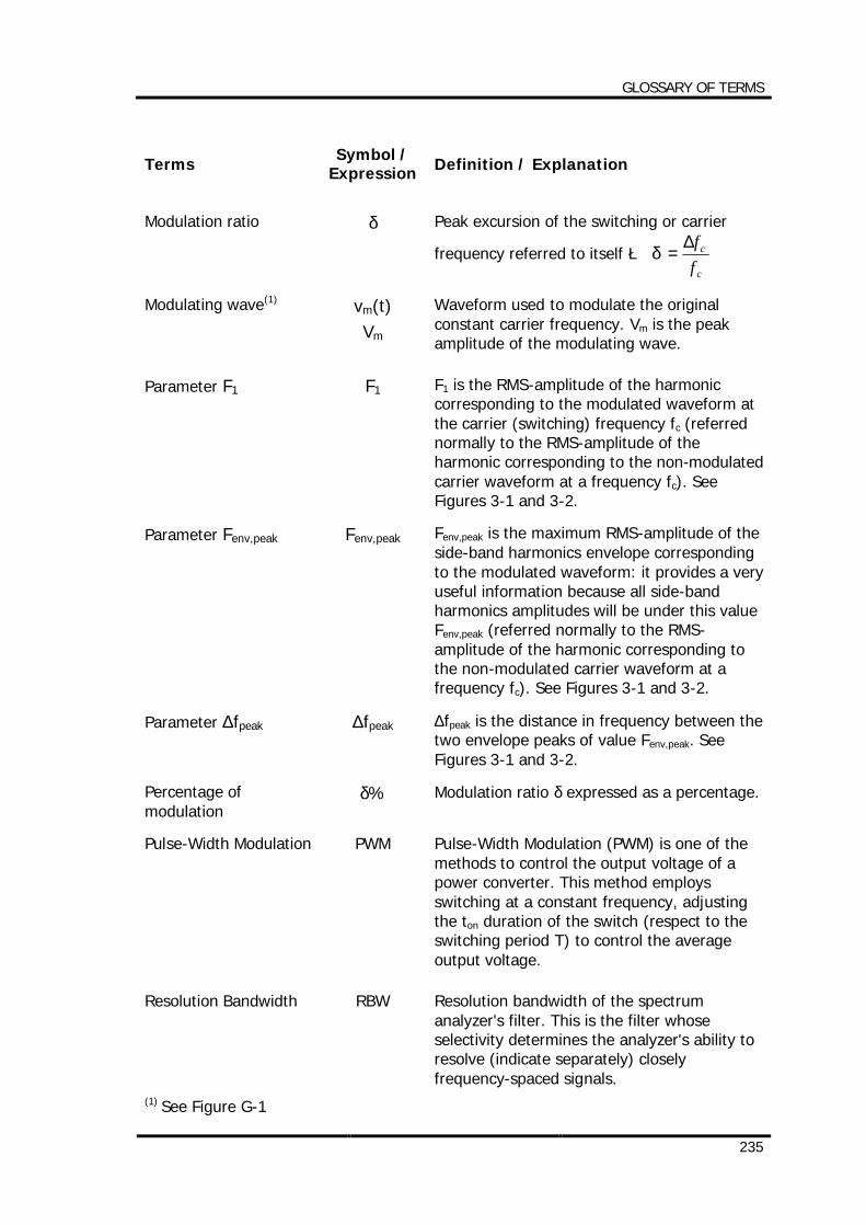
GLOSSARY OF TERMS
235
Terms Symbol / Expression Definition / Explanation
Modulation ratio δ Peak excursion of the switching or carrier
frequency referred to itself è c
c
ff∆
=δ
Modulating wave(1) vm(t) Vm
Waveform used to modulate the original constant carrier frequency. Vm is the peak amplitude of the modulating wave.
Parameter F1 F1 F1 is the RMS-amplitude of the harmonic corresponding to the modulated waveform at the carrier (switching) frequency fc (referred normally to the RMS-amplitude of the harmonic corresponding to the non-modulated carrier waveform at a frequency fc). See Figures 3-1 and 3-2.
Parameter Fenv,peak Fenv,peak Fenv,peak is the maximum RMS-amplitude of the side-band harmonics envelope corresponding to the modulated waveform: it provides a very useful information because all side-band harmonics amplitudes will be under this value Fenv,peak (referred normally to the RMS-amplitude of the harmonic corresponding to the non-modulated carrier waveform at a frequency fc). See Figures 3-1 and 3-2.
Parameter ∆fpeak ∆fpeak ∆fpeak is the distance in frequency between the two envelope peaks of value Fenv,peak. See Figures 3-1 and 3-2.
Percentage of modulation
δ% Modulation ratio δ expressed as a percentage.
Pulse-Width Modulation PWM Pulse-Width Modulation (PWM) is one of the methods to control the output voltage of a power converter. This method employs switching at a constant frequency, adjusting the ton duration of the switch (respect to the switching period T) to control the average output voltage.
Resolution Bandwidth RBW Resolution bandwidth of the spectrum analyzer's filter. This is the filter whose selectivity determines the analyzer's ability to resolve (indicate separately) closely frequency-spaced signals.
(1) See Figure G-1
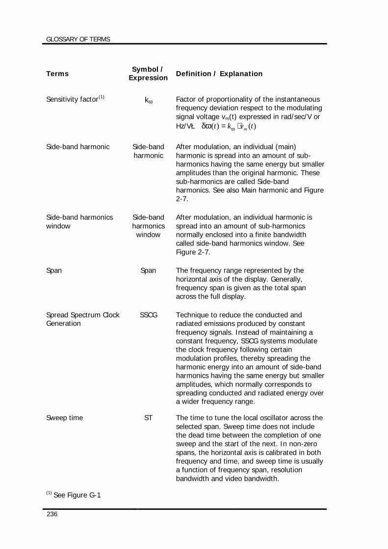
GLOSSARY OF TERMS
236
Terms Symbol / Expression Definition / Explanation
Sensitivity factor(1) kω Factor of proportionality of the instantaneous
frequency deviation respect to the modulating signal voltage vm(t) expressed in rad/sec/V or Hz/Vè )()( tvkt m⋅= ωδω
Side-band harmonic Side-band harmonic
After modulation, an individual (main) harmonic is spread into an amount of sub-harmonics having the same energy but smaller amplitudes than the original harmonic. These sub-harmonics are called Side-band harmonics. See also Main harmonic and Figure 2-7.
Side-band harmonics window
Side-band harmonics window
After modulation, an individual harmonic is spread into an amount of sub-harmonics normally enclosed into a finite bandwidth called side-band harmonics window. See Figure 2-7.
Span Span The frequency range represented by the horizontal axis of the display. Generally, frequency span is given as the total span across the full display.
Spread Spectrum Clock Generation
SSCG Technique to reduce the conducted and radiated emissions produced by constant frequency signals. Instead of maintaining a constant frequency, SSCG systems modulate the clock frequency following certain modulation profiles, thereby spreading the harmonic energy into an amount of side-band harmonics having the same energy but smaller amplitudes, which normally corresponds to spreading conducted and radiated energy over a wider frequency range.
Sweep time ST The time to tune the local oscillator across the selected span. Sweep time does not include the dead time between the completion of one sweep and the start of the next. In non-zero spans, the horizontal axis is calibrated in both frequency and time, and sweep time is usually a function of frequency span, resolution bandwidth and video bandwidth.
(1) See Figure G-1
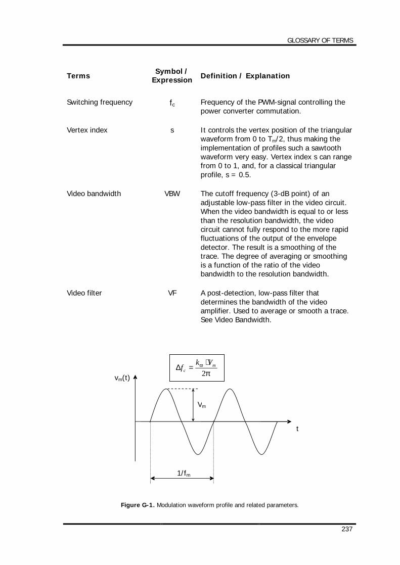
GLOSSARY OF TERMS
237
Terms Symbol / Expression Definition / Explanation
Switching frequency fc Frequency of the PWM-signal controlling the
power converter commutation.
Vertex index s It controls the vertex position of the triangular waveform from 0 to Tm/2, thus making the implementation of profiles such a sawtooth waveform very easy. Vertex index s can range from 0 to 1, and, for a classical triangular profile, s = 0.5.
Video bandwidth VBW The cutoff frequency (3-dB point) of an adjustable low-pass filter in the video circuit. When the video bandwidth is equal to or less than the resolution bandwidth, the video circuit cannot fully respond to the more rapid fluctuations of the output of the envelope detector. The result is a smoothing of the trace. The degree of averaging or smoothing is a function of the ratio of the video bandwidth to the resolution bandwidth.
Video filter VF A post-detection, low-pass filter that determines the bandwidth of the video amplifier. Used to average or smooth a trace. See Video Bandwidth.
Figure G-1. Modulation waveform profile and related parameters.
t
vm(t)
1/fm
Vm
πω
2m
cVk
f⋅
=∆

ANNEXES
ANNEX 1 ANNEX 2 ANNEX 3 ANNEX 4 ANNEX 5 ANNEX 6 ANNEX 7

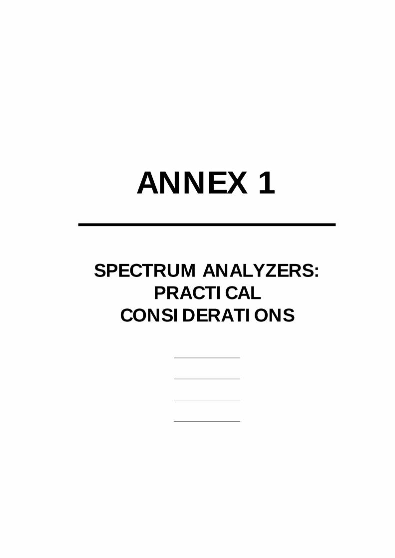
ANNEX 1
SPECTRUM ANALYZERS: PRACTICAL
CONSIDERATIONS

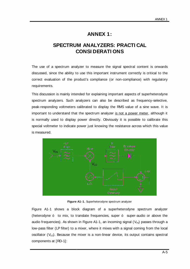
ANNEX 1
A-5
ANNEX 1:
SPECTRUM ANALYZERS: PRACTICAL CONSIDERATIONS
The use of a spectrum analyzer to measure the signal spectral content is onwards
discussed, since the ability to use this important instrument correctly is critical to the
correct evaluation of the product's compliance (or non-compliance) with regulatory
requirements.
This discussion is mainly intended for explaining important aspects of superheterodyne
spectrum analyzers. Such analyzers can also be described as frequency-selective,
peak-responding voltmeters calibrated to display the RMS value of a sine wave. It is
important to understand that the spectrum analyzer is not a power meter, although it
is normally used to display power directly. Obviously it is possible to calibrate this
special voltmeter to indicate power just knowing the resistance across which this value
is measured.
Figure A1-1. Superheterodyne spectrum analyzer
Figure A1-1 shows a block diagram of a superheterodyne spectrum analyzer
(heterodyne ó to mix, to translate frequencies, super ó super-audio or above the
audio frequencies). As shown in Figure A1-1, an incoming signal (VIN) passes through a
low-pass filter (LP filter) to a mixer, where it mixes with a signal coming from the local
oscillator (VLO). Because the mixer is a non-linear device, its output contains spectral
components at [RD-1]:
VLO
VIN
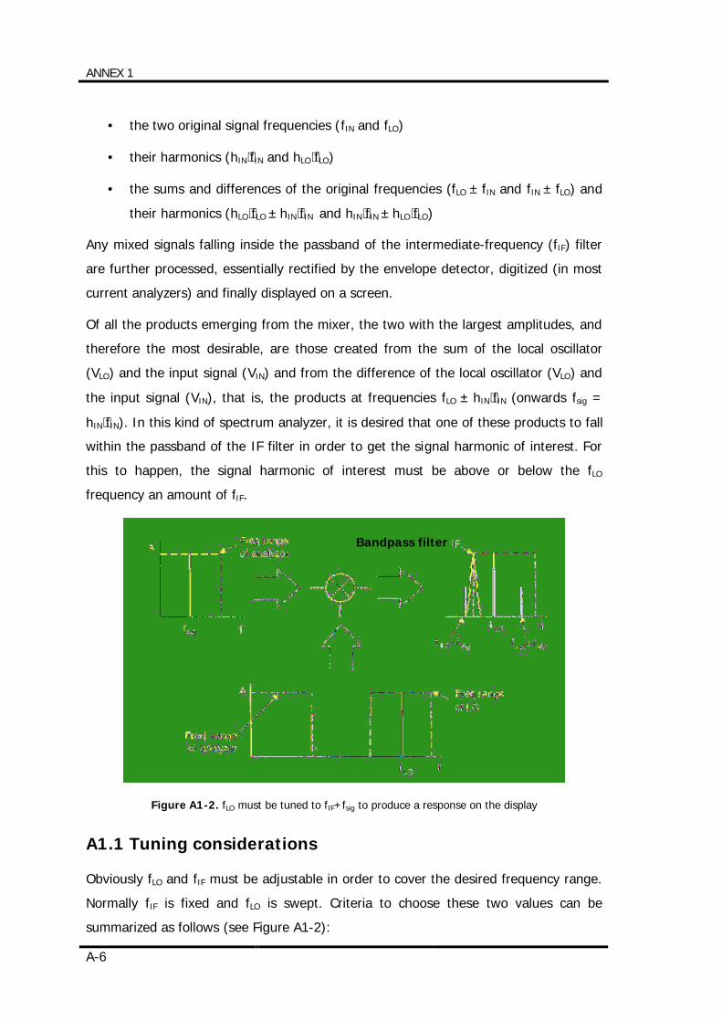
ANNEX 1
A-6
• the two original signal frequencies (fIN and fLO)
• their harmonics (hIN⋅fIN and hLO⋅fLO)
• the sums and differences of the original frequencies (fLO ± fIN and fIN ± fLO) and
their harmonics (hLO⋅fLO ± hIN⋅fIN and hIN⋅fIN ± hLO⋅fLO)
Any mixed signals falling inside the passband of the intermediate-frequency (fIF) filter
are further processed, essentially rectified by the envelope detector, digitized (in most
current analyzers) and finally displayed on a screen.
Of all the products emerging from the mixer, the two with the largest amplitudes, and
therefore the most desirable, are those created from the sum of the local oscillator
(VLO) and the input signal (VIN) and from the difference of the local oscillator (VLO) and
the input signal (VIN), that is, the products at frequencies fLO ± hIN⋅fIN (onwards fsig =
hIN⋅fIN). In this kind of spectrum analyzer, it is desired that one of these products to fall
within the passband of the IF filter in order to get the signal harmonic of interest. For
this to happen, the signal harmonic of interest must be above or below the fLO
frequency an amount of fIF.
Figure A1-2. fLO must be tuned to fIF+fsig to produce a response on the display
A1.1 Tuning considerations
Obviously fLO and fIF must be adjustable in order to cover the desired frequency range.
Normally fIF is fixed and fLO is swept. Criteria to choose these two values can be
summarized as follows (see Figure A1-2):
Bandpass filter
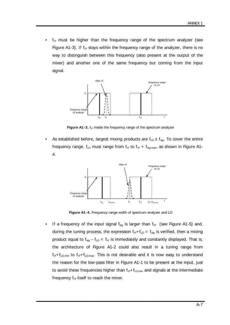
ANNEX 1
A-7
• fIF must be higher than the frequency range of the spectrum analyzer (see
Figure A1-3). If fIF stays within the frequency range of the analyzer, there is no
way to distinguish between this frequency (also present at the output of the
mixer) and another one of the same frequency but coming from the input
signal.
Figure A1-3. fIF inside the frequency range of the spectrum analyzer
• As established before, largest mixing products are fLO ± fsig. To cover the entire
frequency range, fLO must range from fIF to fIF + fsig,max, as shown in Figure A1-
4.
Figure A1-4. Frequency range width of spectrum analyzer and LO
• If a frequency of the input signal fsig is larger than fIF (see Figure A1-5) and,
during the tuning process, the expression fIF+fLO = fsig is verified, then a mixing
product equal to fsig – fLO = fIF is immediately and constantly displayed. That is,
the architecture of Figure A1-2 could also result in a tuning range from
fIF+fLO,min to fIF+fLO,max. This is not desirable and it is now easy to understand
the reason for the low-pass filter in Figure A1-1 to be present at the input, just
to avoid these frequencies higher than fIF+fLO,min and signals at the intermediate
frequency fIF itself to reach the mixer.
Filter IF
Frequency range of analyzer
Frequency range of LO
f
A
fLO fIF fsig fsig,max fIF+fsig,max
Filter IF
Frequency range of analyzer
Frequency range of LO
f
A
fLO fIF fsig
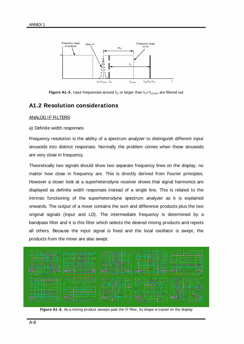
ANNEX 1
A-8
Figure A1-5. Input frequencies around fIF or larger than fIF+fLO,min are filtered out
A1.2 Resolution considerations
ANALOG IF FILTERS:
a) Definite width responses
Frequency resolution is the ability of a spectrum analyzer to distinguish different input
sinusoids into distinct responses. Normally the problem comes when these sinusoids
are very close in frequency.
Theoretically two signals should show two separate frequency lines on the display, no
matter how close in frequency are. This is directly derived from Fourier principles.
However a closer look at a superheterodyne receiver shows that signal harmonics are
displayed as definite width responses instead of a single line. This is related to the
intrinsic functioning of the superheterodyne spectrum analyzer as it is explained
onwards. The output of a mixer contains the sum and difference products plus the two
original signals (input and LO). The intermediate frequency is determined by a
bandpass filter and it is this filter which selects the desired mixing products and rejects
all others. Because the input signal is fixed and the local oscillator is swept, the
products from the mixer are also swept.
Figure A1-6. As a mixing product sweeps past the IF filter, its shape is traced on the display
Frequency range of LO
f
A
fIF=fLO,min fsig=fIF+fLO
∆fLO
Frequency range of analyzer
Filter IF
fIF
fLO,max fLO
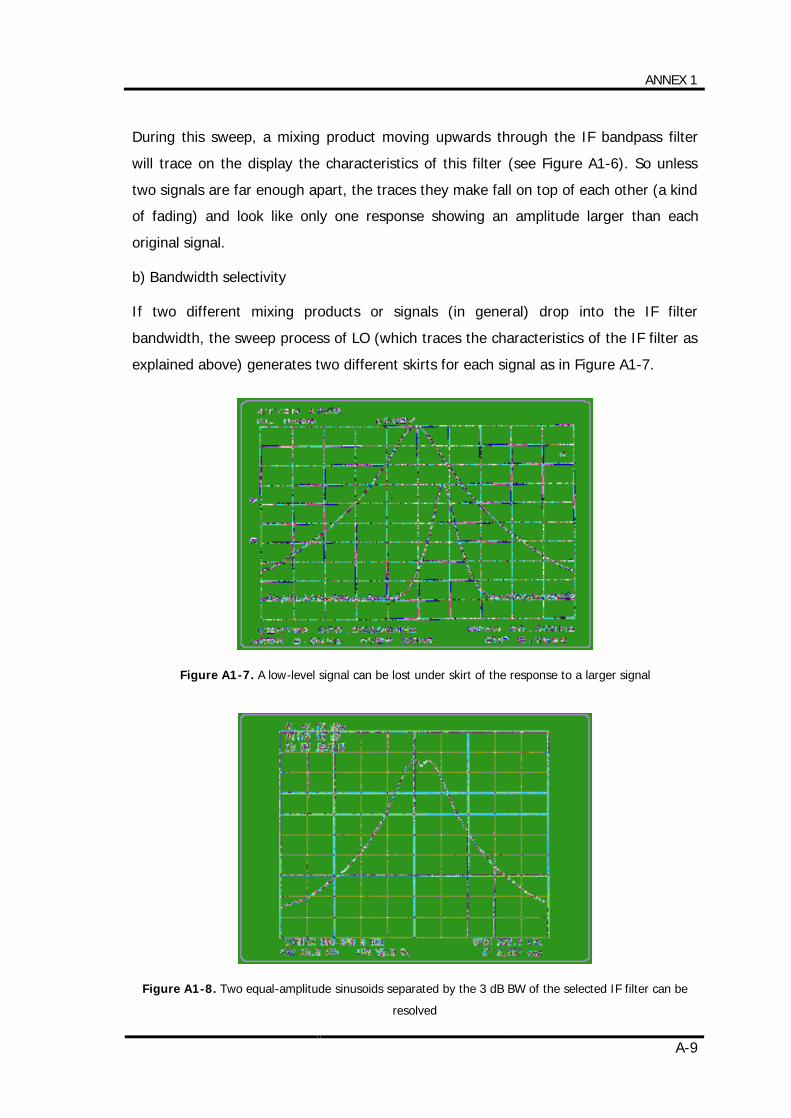
ANNEX 1
A-9
During this sweep, a mixing product moving upwards through the IF bandpass filter
will trace on the display the characteristics of this filter (see Figure A1-6). So unless
two signals are far enough apart, the traces they make fall on top of each other (a kind
of fading) and look like only one response showing an amplitude larger than each
original signal.
b) Bandwidth selectivity
If two different mixing products or signals (in general) drop into the IF filter
bandwidth, the sweep process of LO (which traces the characteristics of the IF filter as
explained above) generates two different skirts for each signal as in Figure A1-7.
Figure A1-7. A low-level signal can be lost under skirt of the response to a larger signal
Figure A1-8. Two equal-amplitude sinusoids separated by the 3 dB BW of the selected IF filter can be
resolved

ANNEX 1
A-10
If these two signals have different amplitudes (more usual than not), the smaller signal
can be lost under the skirt of the response traced out by the larger, as seen in Figure
A1-7. In the case of two sinusoidal waveforms of equal amplitude, the resolution of the
3 dB BW of the IF filter can resolve this two signals as shown in Figure A1-8.
Another specification must be defined to take this feature into account: bandwidth
selectivity. Normally this parameter is specified as the ratio of the 60 dB to the 3 dB
bandwidths, as shown in Figure A1-9 (every manufacturer specifies its own bandwidth
selectivity, like 60:6 dB, 25:1 dB, etc)
Figure A1-9. Bandwidth selectivity, ratio of 60 dB to 3 dB bandwidths
Taking two signals separate ∆fsig in frequency and differing ∆dBsig in amplitude and
assuming a logarithmic amplitude and a linear frequency scale for the spectrum
analyzer, it can be assumed that the filter skirt is straight between the two points
defining bandwidth selectivity, i.e., between BWH and BWL, when a ratio H:L dB is
selected (for instance, 60:3 dB implies ∆dBH = 60 dB and ∆dBL = 3 dB).
From Figure A1-10, the following expression (A1-1) can be derived:
22LH
LHsigsig BWBW
dBdBfdB−
∆−∆⋅∆=∆ (A1-1)
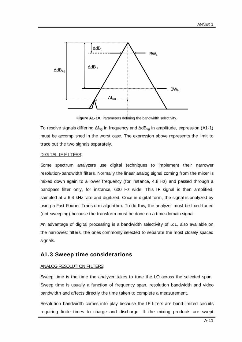
ANNEX 1
A-11
Figure A1-10. Parameters defining the bandwidth selectivity.
To resolve signals differing ∆fsig in frequency and ∆dBsig in amplitude, expression (A1-1)
must be accomplished in the worst case. The expression above represents the limit to
trace out the two signals separately.
DIGITAL IF FILTERS:
Some spectrum analyzers use digital techniques to implement their narrower
resolution-bandwidth filters. Normally the linear analog signal coming from the mixer is
mixed down again to a lower frequency (for instance, 4.8 Hz) and passed through a
bandpass filter only, for instance, 600 Hz wide. This IF signal is then amplified,
sampled at a 6.4 kHz rate and digitized. Once in digital form, the signal is analyzed by
using a Fast Fourier Transform algorithm. To do this, the analyzer must be fixed-tuned
(not sweeping) because the transform must be done on a time-domain signal.
An advantage of digital processing is a bandwidth selectivity of 5:1, also available on
the narrowest filters, the ones commonly selected to separate the most closely spaced
signals.
A1.3 Sweep time considerations
ANALOG RESOLUTION FILTERS:
Sweep time is the time the analyzer takes to tune the LO across the selected span.
Sweep time is usually a function of frequency span, resolution bandwidth and video
bandwidth and affects directly the time taken to complete a measurement.
Resolution bandwidth comes into play because the IF filters are band-limited circuits
requiring finite times to charge and discharge. If the mixing products are swept
BWL
BWH
∆dBH ∆dBsig
∆fsig
∆dBL

ANNEX 1
A-12
through them too fast, there will be a loss of displayed amplitude as shown in Figure
A1-11 (see also envelope detector considerations below).
Figure A1-11. Sweeping too fast causes a drop in the displayed amplitude and a shift in the indicated frequency
The time a mixing product stays within the passband of the IF filter is expressed as
follows:
Time in passband =SpanRBWST ⋅ (A1 -2)
where:
• RBW is the resolution bandwidth
• ST is the sweep time
• Span is the frequency range represented by the horizontal axis of the display,
commonly distributed across the full ten divisions in a spectrum analyzer.
On the other hand, the rise time of a filter is inversely proportional to its bandwidth
this way:
Rise time = RBW
k (A1 -3)
where k is a constant of proportionality between 2 and 15.
Making the times in (A1-2) and (A1-3) equal and solving for sweep time, it is obtained:

ANNEX 1
A-13
2RBWSpankST ⋅= (A1 -4)
An important message is obtained from the expression above: a change in the
resolution bandwidth (RBW) has a dramatic effect on the sweep time in order to
maintain a calibrated display. If a sweep time longer than the maximum available in
the analyzer is called for, a message of uncalibrated display appears.
DIGITAL RESOLUTION FILTERS:
Effects of digital resolution filters are normally different from those related to analog
filters. The signal being analyzed is processed in, for instance, 600 Hz blocks. When
selecting the 10 Hz resolution bandwidth, the analyzer is in effect simultaneously
processing the data in each 600 Hz block through 60 contiguous 10 Hz filters. If the
digital processing were instantaneous, a factor-of-60 reduction in sweep time could be
expected; in practice it is lower but significant nonetheless.
A1.4 Envelope detector considerations
Spectrum analyzers convert the IF signal to video with an envelope detector. Figure
A1-12 shows the simplest implementation of such a detector.
Figure A1-12. Envelope detector
Detector time constants are such that the voltage across the capacitor equals the peak
value of the IF signal at all times, that is, the detector can follow the fastest possible
changes in the envelope of the IF signal but not the instantaneous value of the IF
signal itself.
This IF signal comes from a bandpass filter whose resolution bandwidth is selectable.
Normally, this bandwidth is adjusted in order to distinguish each spectral component of
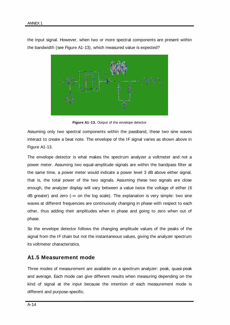
ANNEX 1
A-14
the input signal. However, when two or more spectral components are present within
the bandwidth (see Figure A1-13), which measured value is expected?
Figure A1-13. Output of the envelope detector
Assuming only two spectral components within the passband, these two sine waves
interact to create a beat note. The envelope of the IF signal varies as shown above in
Figure A1-13.
The envelope detector is what makes the spectrum analyzer a voltmeter and not a
power meter. Assuming two equal-amplitude signals are within the bandpass filter at
the same time, a power meter would indicate a power level 3 dB above either signal,
that is, the total power of the two signals. Assuming these two signals are close
enough, the analyzer display will vary between a value twice the voltage of either (6
dB greater) and zero (-∞ on the log scale). The explanation is very simple: two sine
waves at different frequencies are continuously changing in phase with respect to each
other, thus adding their amplitudes when in phase and going to zero when out of
phase.
So the envelope detector follows the changing amplitude values of the peaks of the
signal from the IF chain but not the instantaneous values, giving the analyzer spectrum
its voltmeter characteristics.
A1.5 Measurement mode
Three modes of measurement are available on a spectrum analyzer: peak, quasi-peak
and average. Each mode can give different results when measuring depending on the
kind of signal at the input because the intention of each measurement mode is
different and purpose-specific.
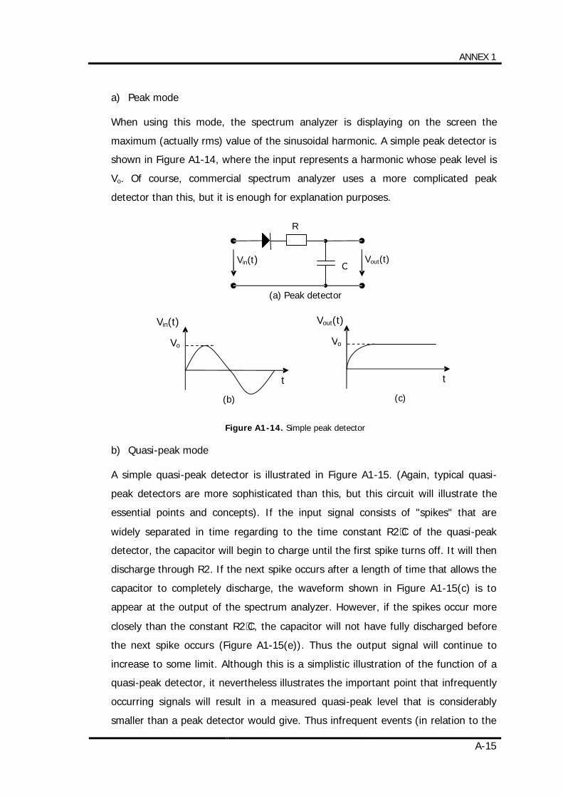
ANNEX 1
A-15
a) Peak mode
When using this mode, the spectrum analyzer is displaying on the screen the
maximum (actually rms) value of the sinusoidal harmonic. A simple peak detector is
shown in Figure A1-14, where the input represents a harmonic whose peak level is
Vo. Of course, commercial spectrum analyzer uses a more complicated peak
detector than this, but it is enough for explanation purposes.
Figure A1-14. Simple peak detector
b) Quasi-peak mode
A simple quasi-peak detector is illustrated in Figure A1-15. (Again, typical quasi-
peak detectors are more sophisticated than this, but this circuit will illustrate the
essential points and concepts). If the input signal consists of "spikes" that are
widely separated in time regarding to the time constant R2⋅C of the quasi-peak
detector, the capacitor will begin to charge until the first spike turns off. It will then
discharge through R2. If the next spike occurs after a length of time that allows the
capacitor to completely discharge, the waveform shown in Figure A1-15(c) is to
appear at the output of the spectrum analyzer. However, if the spikes occur more
closely than the constant R2⋅C, the capacitor will not have fully discharged before
the next spike occurs (Figure A1-15(e)). Thus the output signal will continue to
increase to some limit. Although this is a simplistic illustration of the function of a
quasi-peak detector, it nevertheless illustrates the important point that infrequently
occurring signals will result in a measured quasi-peak level that is considerably
smaller than a peak detector would give. Thus infrequent events (in relation to the
t
Vin(t)
Vo
Vin(t) Vout(t)
(a) Peak detector
t
Vout(t)
Vo
R
C
(b) (c)
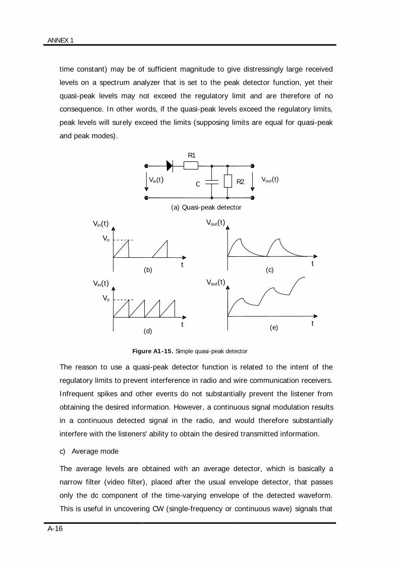
ANNEX 1
A-16
time constant) may be of sufficient magnitude to give distressingly large received
levels on a spectrum analyzer that is set to the peak detector function, yet their
quasi-peak levels may not exceed the regulatory limit and are therefore of no
consequence. In other words, if the quasi-peak levels exceed the regulatory limits,
peak levels will surely exceed the limits (supposing limits are equal for quasi-peak
and peak modes).
Figure A1-15. Simple quasi-peak detector
The reason to use a quasi-peak detector function is related to the intent of the
regulatory limits to prevent interference in radio and wire communication receivers.
Infrequent spikes and other events do not substantially prevent the listener from
obtaining the desired information. However, a continuous signal modulation results
in a continuous detected signal in the radio, and would therefore substantially
interfere with the listeners' ability to obtain the desired transmitted information.
c) Average mode
The average levels are obtained with an average detector, which is basically a
narrow filter (video filter), placed after the usual envelope detector, that passes
only the dc component of the time-varying envelope of the detected waveform.
This is useful in uncovering CW (single-frequency or continuous wave) signals that
t
Vin(t)
Vo
Vin(t) Vout(t)
(a) Quasi-peak detector
t
Vout(t)
C R2
t
Vin(t)
Vo
t
Vout(t)
(b) (c)
(d) (e)
R1
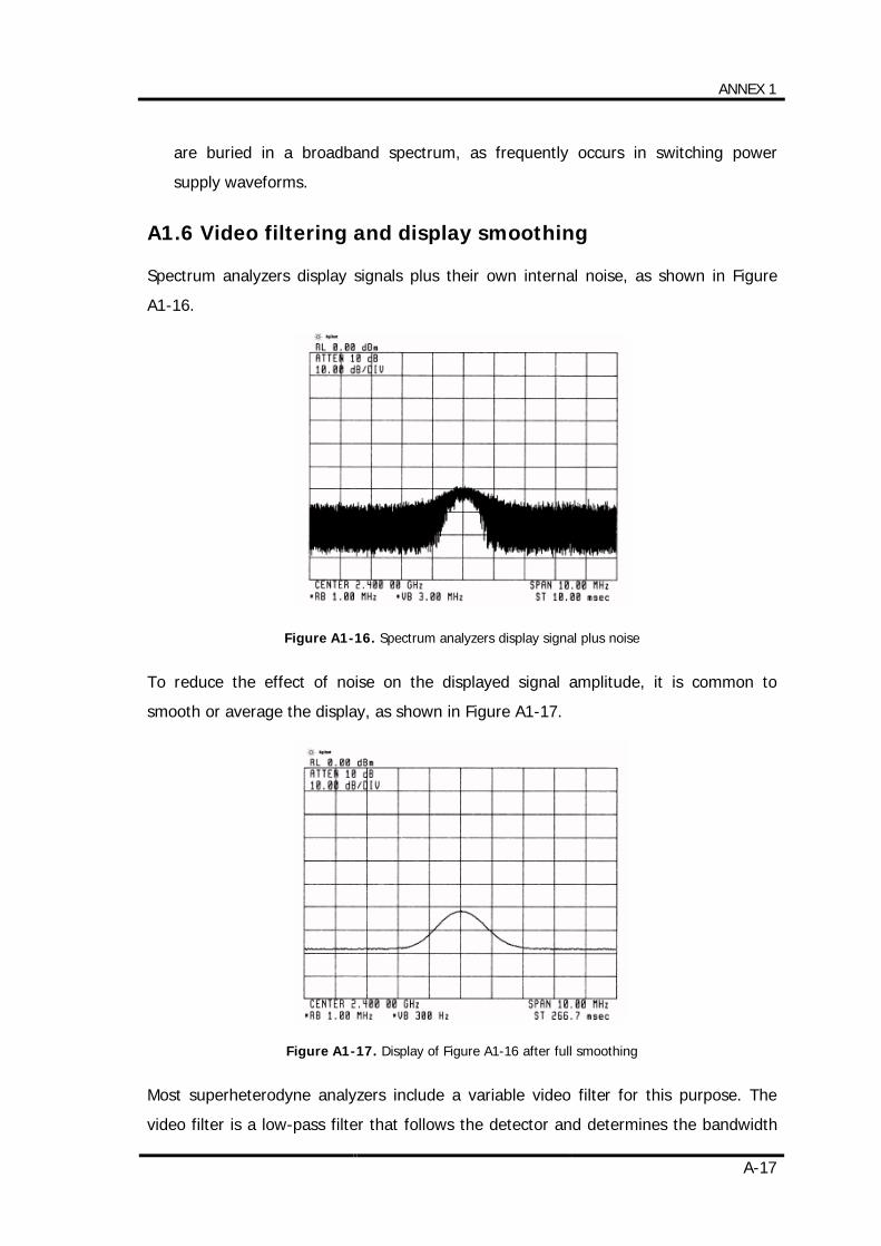
ANNEX 1
A-17
are buried in a broadband spectrum, as frequently occurs in switching power
supply waveforms.
A1.6 Video filtering and display smoothing
Spectrum analyzers display signals plus their own internal noise, as shown in Figure
A1-16.
Figure A1-16. Spectrum analyzers display signal plus noise
To reduce the effect of noise on the displayed signal amplitude, it is common to
smooth or average the display, as shown in Figure A1-17.
Figure A1-17. Display of Figure A1-16 after full smoothing
Most superheterodyne analyzers include a variable video filter for this purpose. The
video filter is a low-pass filter that follows the detector and determines the bandwidth

ANNEX 1
A-18
of the video circuits that drive the vertical deflection system of the display. As the
cutoff frequency of the video filter is reduced to the point at which it becomes equal or
less than the bandwidth of the selected resolution (IF) filter, the video system can no
longer follow the more rapid variations of the envelope of the signals passing through
the IF chain. The result is an averaging or smoothing of the displayed signal when
noisy signals are present while, at the same time, having no effect on constant signals.
Because the video filter has its own response time, the sweep time gets
longer:VBWRBW
SpankST⋅
⋅=
where:
• RBW is the resolution bandwidth
• VBW is the video bandwidth (the cutoff frequency of the adjustable low-pass
filter in the video circuit)
• ST is the sweep time
• Span is the frequency range represented by the horizontal axis of the display,
commonly distributed across the full ten divisions in a spectrum analyzer.
• k is a constant of proportionality between 2 and 15.
Most analyzers that sweep time automatically account for video bandwidth as well as
span and resolution bandwidth.

ANNEX 2
NORMATIVE REQUIREMENTS TO MEASURE EMI

ANNEX 2
A-21
ANNEX 2:
NORMATIVE REQUIREMENTS TO MEASURE EMI
It is important to clearly specify how product emissions must be measured when
attempting to verify compliance with the limits and the limits themselves. Different
interpretations of the same normative can give different results of the measured data
at different measurement sites. Every standard that sets out limits on radiated and
conducted emissions (FCC, CISPR 22 and MIL-STD-461) has a related standard that
clearly defines how the data are to be measured. This includes test procedure, test
equipment, bandwidth, test antennas, etc. The specification of the method for
gathering the data is critically important so that the governing agency can be sure that
data gathered on a product at one company's test site can be validly compared to the
limits and to data gathered at another test site. Otherwise the governing agency as
well as the product manufacturer cannot be assured that the product's emissions
comply with the limits. Onwards, a summary of the measurement procedures that
apply to the FCC ([RE-4], [RE-5]) and CISPR 22 ([RE-1], [RE-2], [RE-3]) requirements
are presented.
A2.1 Radiated emissions
Although radiated emissions are not of complete interest for this thesis, it is worthy to
expose some considerations which are useful for an understanding of measuring EMI.
When measuring conducted perturbations with a spectrum analyzer, it is normally
found a closer relationship between theoretical and measured results, while in the case
of radiated emissions, several antenna and transmission factors affect the measured
results in such a way that some differences may arise between theoretical and
measured values
FCC specifies that the measurements of radiated and conducted emissions must be
performed on the complete system. All interconnect cables to peripheral equipment
must be connected and the system must be in a typical configuration. Cables and
system must also be configured in a representative way such that the emissions are
maximized.
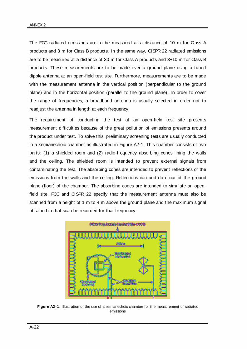
ANNEX 2
A-22
The FCC radiated emissions are to be measured at a distance of 10 m for Class A
products and 3 m for Class B products. In the same way, CISPR 22 radiated emissions
are to be measured at a distance of 30 m for Class A products and 3÷10 m for Class B
products. These measurements are to be made over a ground plane using a tuned
dipole antenna at an open-field test site. Furthermore, measurements are to be made
with the measurement antenna in the vertical position (perpendicular to the ground
plane) and in the horizontal position (parallel to the ground plane). In order to cover
the range of frequencies, a broadband antenna is usually selected in order not to
readjust the antenna in length at each frequency.
The requirement of conducting the test at an open-field test site presents
measurement difficulties because of the great pollution of emissions presents around
the product under test. To solve this, preliminary screening tests are usually conducted
in a semianechoic chamber as illustrated in Figure A2-1. This chamber consists of two
parts: (1) a shielded room and (2) radio-frequency absorbing cones lining the walls
and the ceiling. The shielded room is intended to prevent external signals from
contaminating the test. The absorbing cones are intended to prevent reflections of the
emissions from the walls and the ceiling. Reflections can and do occur at the ground
plane (floor) of the chamber. The absorbing cones are intended to simulate an open-
field site. FCC and CISPR 22 specify that the measurement antenna must also be
scanned from a height of 1 m to 4 m above the ground plane and the maximum signal
obtained in that scan be recorded for that frequency.
Figure A2-1. Illustration of the use of a semianechoic chamber for the measurement of radiated emissions
ANNEX 2
A-23
One final test requirement needs to be addressed. The FCC and CISPR 22 test
procedures specify that the bandwidth (6 dB) of the spectrum analyzer or receiver that
is used to measure the radiated emissions must be at least 100 kHz. If the emission at
a particular frequency is very narrow, such as a clock harmonic, the bandwidth of the
receiver is not of much concern. However, if the emission is due to fairly broadband
source, the bandwidth of the receiver directly determines the signal level that is
measured: the wider the bandwidth, the larger the measured level.
A related issue is the detector used in the output stage of the receiver. Typical
spectrum analyzers use peak detectors that record the maximum signal level at the
desired frequency.
A2.2 Conducted emissions
The intent of the conducted emission limits is to restrict the noise current passing out
through the product's ac power cord. The reason for this is that these noise currents
will be placed on the common power net of the installation. The common power net of
an installation is an array of interconnected wires in the installation walls, and as such,
represents a large antenna. Noise currents that are placed on this power net will
therefore radiate quite efficiently, which can produce interference.
Therefore the conducted emission that should be measured is the noise current
conducted out through the ac power cord of the product. Yet the FCC and CISPR
conducted emissions limits are given in units of volts. This is because the tests are to
be conducted by inserting a line impedance stabilization network (LISN) in series with
the ac power cord of the product. In order to understand the performance of this
device, a summarized overview of the standard ac power distribution system. In
Europe, ac voltage used in residential and business environments has a frequency of
50 Hz and a rms voltage of 220 V (currently, this voltage has been adjusted to 240 V).
This power is transmitted to these sites at various other, higher voltages, by a tri-
phase system, composed of three wires (called phase wires) and a ground wire
connected to earth (neutral wire). The voltage between each two phase wires is 380 V.
At the service entrance panel in the home, the 220 V is obtained between one phase
wire and the neutral one. A forth or safety wire is carried throughout the residence
along with these four wires. Those currents exiting the product via the phase and the
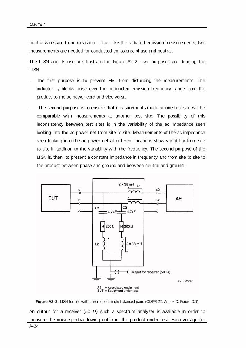
ANNEX 2
A-24
neutral wires are to be measured. Thus, like the radiated emission measurements, two
measurements are needed for conducted emissions, phase and neutral.
The LISN and its use are illustrated in Figure A2-2. Two purposes are defining the
LISN:
− The first purpose is to prevent EMI from disturbing the measurements. The
inductor L1 blocks noise over the conducted emission frequency range from the
product to the ac power cord and vice versa.
− The second purpose is to ensure that measurements made at one test site will be
comparable with measurements at another test site. The possibility of this
inconsistency between test sites is in the variability of the ac impedance seen
looking into the ac power net from site to site. Measurements of the ac impedance
seen looking into the ac power net at different locations show variability from site
to site in addition to the variability with the frequency. The second purpose of the
LISN is, then, to present a constant impedance in frequency and from site to site to
the product between phase and ground and between neutral and ground.
Figure A2-2. LISN for use with unscreened single balanced pairs (CISPR 22, Annex D, Figure D.1)
An output for a receiver (50 Ω) such a spectrum analyzer is available in order to
measure the noise spectra flowing out from the product under test. Each voltage (or
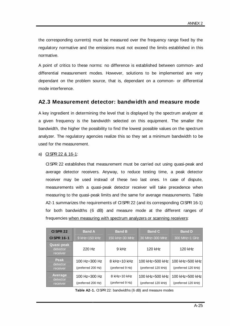
ANNEX 2
A-25
the corresponding currents) must be measured over the frequency range fixed by the
regulatory normative and the emissions must not exceed the limits established in this
normative.
A point of critics to these norms: no difference is established between common- and
differential measurement modes. However, solutions to be implemented are very
dependant on the problem source, that is, dependant on a common- or differential
mode interference.
A2.3 Measurement detector: bandwidth and measure mode
A key ingredient in determining the level that is displayed by the spectrum analyzer at
a given frequency is the bandwidth selected on this equipment. The smaller the
bandwidth, the higher the possibility to find the lowest possible values on the spectrum
analyzer. The regulatory agencies realize this so they set a minimum bandwidth to be
used for the measurement.
a) CISPR 22 & 16-1:
CISPR 22 establishes that measurement must be carried out using quasi-peak and
average detector receivers. Anyway, to reduce testing time, a peak detector
receiver may be used instead of these two last ones. In case of dispute,
measurements with a quasi-peak detector receiver will take precedence when
measuring to the quasi-peak limits and the same for average measurements. Table
A2-1 summarizes the requirements of CISPR 22 (and its corresponding CISPR 16-1)
for both bandwidths (6 dB) and measure mode at the different ranges of
frequencies when measuring with spectrum analyzers or scanning receivers:
CISPR 22
CISPR 16-1
Band A
9 kHz÷150 kHz
Band B
150 kHz÷30 MHz
Band C
30 MHz÷300 MHz
Band D
300 MHz÷1 GHz
Quasi-peak detector receiver
220 Hz 9 kHz 120 kHz 120 kHz
Peak detector receiver
100 Hz÷300 Hz
(preferred 200 Hz)
8 kHz÷10 kHz
(preferred 9 Hz)
100 kHz÷500 kHz
(preferred 120 kHz)
100 kHz÷500 kHz
(preferred 120 kHz)
Average detector receiver
100 Hz÷300 Hz
(preferred 200 Hz)
8 kHz÷10 kHz
(preferred 9 Hz)
100 kHz÷500 kHz
(preferred 120 kHz)
100 kHz÷500 kHz
(preferred 120 kHz)
Table A2-1. CISPR 22: bandwidths (6 dB) and measure modes

ANNEX 2
A-26
From the values listed above, a common bandwidth can be established for the
three measure modes: quasi-peak, peak and average. As it is easy to derive from
Table A2-1, quasi-peak detector values can be taken as the common ones.
b) FEDERAL COMMUNICATIONS COMMISSION (FCC):
As specified at Title 47, Chapter I, Part 15, Subpart A and Section 15.35, on any
frequency or frequencies below or equal to 1000 MHz, the limits are based on
measuring equipment employing a CISPR 16-1 quasi-peak detector function and
related measurement bandwidths, unless otherwise specified. As an alternative to
CISPR quasi-peak measurements, the responsible party, at its option, may
demonstrate compliance with the emission limits using measuring equipment
employing a peak detector function, properly adjusted for such factors as pulse
desensitization, as long as the same bandwidths as indicated for CISPR quasi-peak
measurements are employed. Thus, Table A2-1 above is also valid for FCC
measuring purposes.
ANNEX 3
CONCEPTS OF FOURIER TRANSFORM

ANNEX 3
A-29
ANNEX 3:
CONCEPTS OF FOURIER TRANSFORM
Although this chapter is not intended to be a reference of the Fourier transform, some
concepts and expression must be presented in order to make the understanding of the
thesis easier. Theoretical part of the thesis is completely based on the fundaments of
the Fourier Transform and, moreover, in its computational implementation through the
Fast Fourier Transform (FFT). Literature and references for a wider explanation of
Fourier Transform is numerous and the reader is referred to them ([RD-10], [RD-11]).
The essence of the Fourier transform of a waveform is to decompose or separate the
waveform into a sum of sinusoids of different frequencies. If these sinusoids sum to
the original waveform then the Fourier transform of the waveform has been
determined. The pictorial representation of the Fourier transform is a diagram which
displays the amplitude and frequency of each of the determined sinusoids.
Figure A3-1. Interpretation of the Fourier transform
T/2 -T/2 t
Waveform defined from -∞ to +∞
T/2 -T/2 t
T/2 -T/2 t
T/6 -T/6 t
1
1/2
+
f
1/4
1/2
1/T
3/T
-1/T
-3/T -2/T 2/T
Fourier Transform
Function to be Fourier transformed
Fourier
Transform
-1/2
ANNEX 3
A-30
A usual convention is displaying both positive and negative frequency sinusoids for
each frequency and halving the amplitude accordingly, as shown in Figure A3-1.
The Fourier transform identifies or distinguishes the different frequency sinusoids (and
their respective amplitudes) which combine to form an arbitrary waveform.
Mathematically, this relationship is stated as
∫∞
∞−
⋅⋅⋅−⋅= dtethfH tfj π2)()( (A3 -1)
where h(t) is the waveform to be decomposed into a sum of sinusoids and H(f) is the
Fourier transform of h(t). Note that the Fourier transform is not of easy interpretation
(as expressed above) because it is defined from -∞ to +∞.
It is normally associated the analysis of periodic functions such a square wave with
Fourier series rather than Fourier transforms but it is easy to demonstrate that Fourier
series is a special case of the Fourier transform.
If the waveform h(t) is not periodic then the Fourier transform will be a continuous
function of frequency; that is, h(t) is represented by the summation of sinusoids of all
frequencies. In order to illustrate this aspect, consider the pulse waveform and its
Fourier transform shown in Figure A3-2. In this example, the Fourier transform
indicates that one sinusoid frequency becomes indistinguishable from the next and, as
a result, all frequencies must be considered.
Figure A3-2. Fourier Transform of a pulse waveform
The Fourier transform is then a frequency domain representation of a continuous
function. Of course, both h(t) and H(f) contain the same information differing only in
021T
X(f)
f
T0
A
t
x(t)
-T0
0
1T
023T
021T
−
2AT0
ANNEX 3
A-31
the manner of presenting this information. Fourier analysis allows one to examine a
function from another point of view, the transform domain.
In general, the Fourier transform is a complex quantity:
)()()()()( fjefHfjIfRfH θ⋅=+= (A3-2)
where:
• R(f) is the real part of the Fourier Transform
• I(f) is the imaginary part of the Fourier transform
• |H(f)| is the amplitude of Fourier spectra of h(t) and is given by
)()( 22 fIfR +
• θ(f) is the phase angle of the Fourier transform and is given by
−
)()(tan 1
fRfI
A3.1 Fourier series
In the technical literature, Fourier series is normally developed independently on the
Fourier integral in expression (A3-1). However, with the introduction of distribution
theory, Fourier series can be theoretically derived as a special case of the Fourier
integral.
Fourier series is a common way of expressing any periodic signal as a sum of its
harmonic components [RD-1]:
∑∞
=
+=1
0 )()(h
h tFFtF (A3 -3)
where F0 represents the average (dc) component of the original signal and Fh, each
one of the infinity of harmonics.
Periodic signals can be represented as linear combinations or more basic signals that
are referred to as basis functions and denoted as φn(t):
∑∞
=
⋅=0
)()(n
nn tctx φ (A3 -4)
The trigonometric Fourier series uses the sinusoidal basis functions (orthogonal
functions as required):
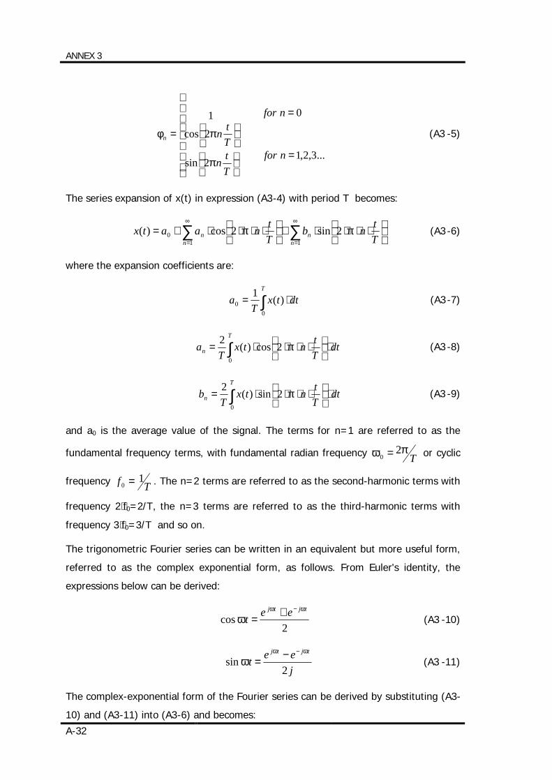
ANNEX 3
A-32
=
=
=
...3,2,1
0
2sin
2cos
1
nfor
nfor
Ttn
Ttnn
π
πφ (A3 -5)
The series expansion of x(t) in expression (A3-4) with period T becomes:
∑∑∞
=
∞
=
⋅⋅⋅⋅+
⋅⋅⋅⋅+=
110 2sin2cos)(
nn
nn T
tnbTtnaatx ππ (A3-6)
where the expansion coefficients are:
∫ ⋅=T
dttxT
a0
0 )(1 (A3-7)
dtTtntx
Ta
T
n ⋅
⋅⋅⋅⋅= ∫
0
2cos)(2π (A3-8)
dtTtntx
Tb
T
n ⋅
⋅⋅⋅⋅= ∫
0
2sin)(2π (A3 -9)
and a0 is the average value of the signal. The terms for n=1 are referred to as the
fundamental frequency terms, with fundamental radian frequency Tπω 2
0 = or cyclic
frequency Tf 10 = . The n=2 terms are referred to as the second-harmonic terms with
frequency 2⋅f0=2/T, the n=3 terms are referred to as the third-harmonic terms with
frequency 3⋅f0=3/T and so on.
The trigonometric Fourier series can be written in an equivalent but more useful form,
referred to as the complex exponential form, as follows. From Euler's identity, the
expressions below can be derived:
2cos
tjtj eetωω
ω−+
= (A3 -10)
jeet
tjtj
2sin
ωω
ω−−
= (A3 -11)
The complex-exponential form of the Fourier series can be derived by substituting (A3-
10) and (A3-11) into (A3-6) and becomes:
ANNEX 3
A-33
∑∞=
−∞=
⋅=n
n
tjnn ectx 0)( ω (A3 -12)
where the expansion coefficients are given by:
∫ −⋅=T
tjnn dtetx
Tc
0
0)(1 ω (A3 -13)
Note that the complex form of the Fourier series contains, in addition to positive-
valued harmonic frequencies ω0, 2ω0, 3ω0,…, negative-valued harmonics -ω0, -2ω0, -
3ω0,… In addition, the expansion coefficients cn may be complex-valued, whereas the
expansion coefficients in the trigonometric Fourier series are real-valued. At first
glance, it may seem that the physical intuition present in the trigonometric Fourier
series has been lost in the complex form, but this is not the case. Note that for each
positive value of n there is a corresponding negative value of n. Coefficients cn and c-n
are the conjugates of each other:
∫ =⋅=−
T
ntjn
n cdtetxT
c0
*0)(1 ω (A3 -14)
and can also be expressed as follows:
ncjnnnn ecccc ∠⋅=∠= (A3 -15)
ncjnn ecc ∠−⋅=* (A3 -16)
The complex-exponential form in expression (A3-12) may be written as
∑∑−∞
−=
∞
=
⋅+⋅+=11
000)(
n
tjnn
n
tjnn ececctx ωω (A3 -17)
Changing the second summation to positive n gives:
∑∑∞
=
−∞
=
⋅+⋅+=1
*
10
00)(n
tjnn
n
tjnn ececctx ωω (A3 -18)
Substituting (A3-15) and (A3-16) into (A3-18) gives:
∑∑∞
=
∠+−∞
=
∠+ ⋅+⋅+=1
)(
1
)(0
00)(n
ctnjn
n
ctnjn
nn ececctx ωω (A3 -19)
ANNEX 3
A-34
( ))()(
10
00 nn ctnjctnj
nn eecc ∠+−∠+
∞
=
++= ∑ ωω (A3 -20)
( )∑∞
=
∠+⋅⋅+=1
00 cos2)(n
nn ctncctx ω (A3 -21)
Therefore, in order to obtain the expansion coefficients for the one-sided spectrum
(positive frequencies only), the coefficients cn for the double-sided spectrum must be
doubled while the dc component remains unchanged. Note that expression (A3-21) is
formally identical to that exposed in expression (A3-3).
A3.2 Discrete Fourier transform
Because of the wide range of problems which are susceptible to be solved by means of
the Fourier transform, particularly the spectral components of a waveform as a result
of a modulation process, it is expected the logical extension of Fourier transform to the
digital computation. However, discretization implies the answer to the difficult question
of knowing how the discrete Fourier Transform relates to the continuous Fourier
Transform. In order to answer this question, it is normally found preferable to derive
the discrete Fourier Transform as a special case of the continuous Fourier transform
theory.
Numerical integration of equation (A3-1) implies the relationship
1,,1,0)()(1
0
/2 −=⋅= ∑−
=
⋅⋅⋅⋅− NnekThNTnH
N
k
Nknj Lπ (A3-22)
Expression (A3-22) is also known as Discrete Fourier Transform where:
• T is the sampling interval.
• N is the number of equidistant samples inside the truncation interval T0.
The expression (A3-22) relates N samples of time and N samples of frequency by
means of the continuous Fourier transform. The discrete Fourier transform is then a
special case of the continuous Fourier transform. If it is assumed that the N samples of
the original function h(t) are one period of a periodic waveform, the Fourier transform
of this periodic function is given by the N samples as computed by (A3-22).
The discrete Fourier is of interest primarily because it approximates the continuous
Fourier transform. The validity and accuracy of this approximation is strictly related to
ANNEX 3
A-35
the waveform under analysis. Differences normally arise because of the discrete
transform requirements for sampling and truncation. Onwards, a special attention will
be focused on the band-limited periodic functions where the truncation interval is equal
to the period of the signal, because these are the kind of signals to be found through
the development of the thesis.
A3.2.1 Band-Limited Periodic Waveforms: Truncation Interval
Equal to Period
Consider the function h(t) and its Fourier transform illustrated in Figure A3-3. The idea
is to sample h(t), truncate the sampled function to N samples and, finally, apply the
discrete Fourier transform according to expression (A3-22). A graphical development of
this process is shown is Figure A3-3. Waveform h(t) is sampled by multiplication with
the sampling function illustrated in Figure A3-3(b). Sampled waveform h(kT) and its
Fourier transform are illustrated in Figure A3-3(c). Note that for this example there is
no aliasing and that, as a result from time domain sampling, the frequency domain has
been scaled by the factor 1/T; the Fourier transform impulse now has an area of A/2T
rather than the original area of A/2. The sampled waveform is truncated by
multiplication with the rectangular function illustrated in Figure A3-3(d); Figure A3-3(e)
illustrates the sampled and truncated waveform. As shown, the rectangular function
was selected so that the N sample values remaining after truncation equate to one
period of the original waveform h(t).
The Fourier transform of the finite length sampled waveform [Figure A3-3(e)] is
obtained by convolving the frequency domain impulse functions of Figure A3-3(c) and
the sin f/f frequency function of Figure A3-3(d). Figure A3-3(e) illustrates the
convolution results: an expanded view of this convolution is shown in Figure A3-4(b). A
sin f/f function (dashed line) is centered on each impulse of Figure A3-4(a) and the
resultant waveforms are additively combined (solid line) to form the convolution result.
With respect to the original transform H(f), the convolved frequency function [Figure
A3-4(b)] is significantly distorted. However, when this function is sampled by the
frequency sampling function illustrated in Figure A3-3(f) the distortion is eliminated.
This follows because the equidistant impulses of the frequency sampling functions are
separated by 1/T0; at these frequencies the solid line of Figure A3-4(b) is zero except
at the frequency 1/T0.
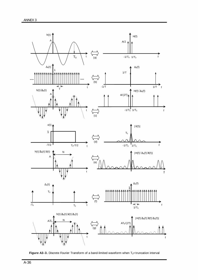
ANNEX 3
A-36
Figure A3-3. Discrete Fourier Transform of a band-limited waveform when T0=truncation interval
T0 t
A
t
A
t
∆0(t)
h(t)⋅∆0(t)
T0-T/2
1
-T/2 t
t
h(t)⋅∆0(t)⋅x(t)
A
x(t)
N
T0
T0
-T0 t
t
A⋅T0
h(t)⋅∆0(t)⋅x(t)⋅∆1(t)
N
T
A/2
f 1/T0 -1/T0
T0
1/T0 -1/T0
|X(f)|
A/(2T)
1/T -1/T
1/T
∆1(t)
∆0(f)
H(f)⋅ ∆0(f)
|H(f)⋅ ∆0(f)⋅X(f)|
AT0/(2T)
|H(f)⋅∆0(f)⋅X(f)⋅∆1(f)|
1
1/T0
f
f
f
f
f
f
1/T0 -1/T0
∆1(f)
H(f)
1
(a)
(b)
(c)
(d)
(e)
(f)
(g)
h(t)
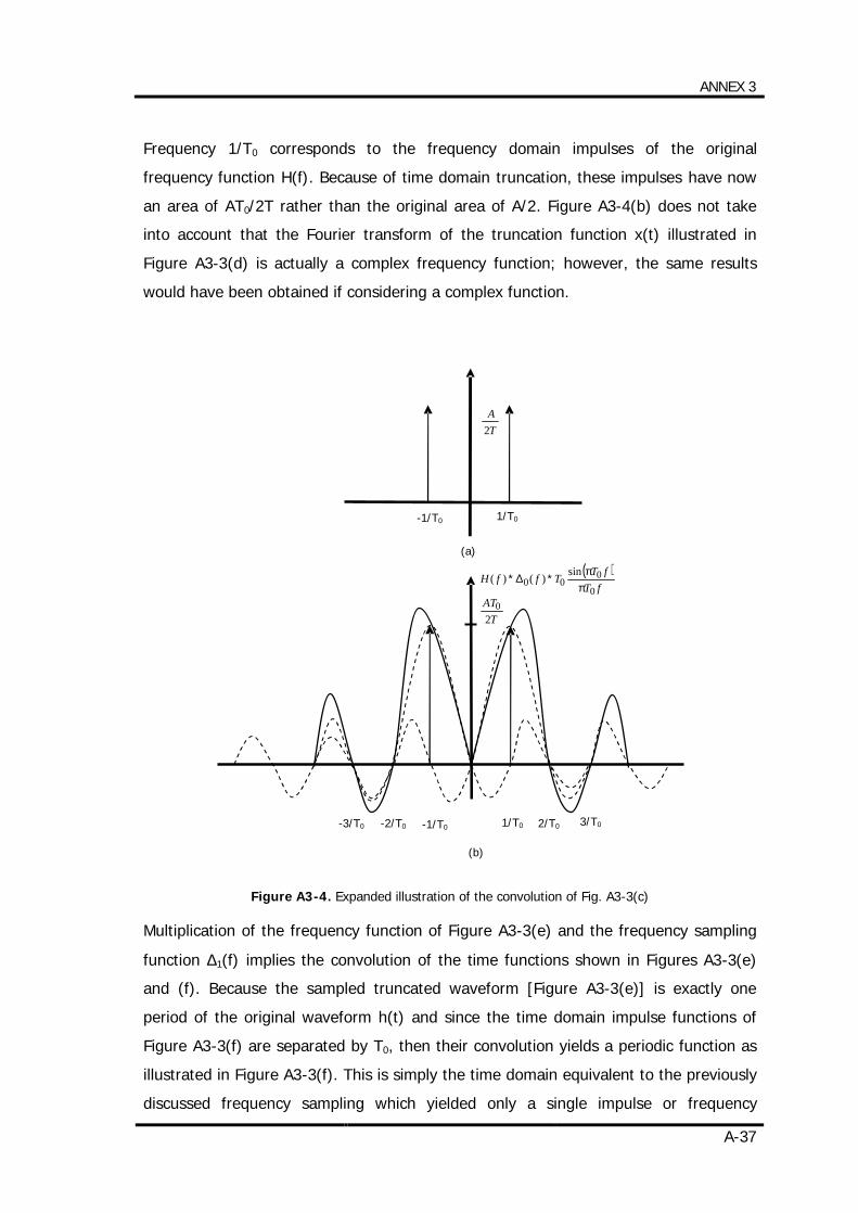
ANNEX 3
A-37
Frequency 1/T0 corresponds to the frequency domain impulses of the original
frequency function H(f). Because of time domain truncation, these impulses have now
an area of AT0/2T rather than the original area of A/2. Figure A3-4(b) does not take
into account that the Fourier transform of the truncation function x(t) illustrated in
Figure A3-3(d) is actually a complex frequency function; however, the same results
would have been obtained if considering a complex function.
Figure A3-4. Expanded illustration of the convolution of Fig. A3-3(c)
Multiplication of the frequency function of Figure A3-3(e) and the frequency sampling
function ∆1(f) implies the convolution of the time functions shown in Figures A3-3(e)
and (f). Because the sampled truncated waveform [Figure A3-3(e)] is exactly one
period of the original waveform h(t) and since the time domain impulse functions of
Figure A3-3(f) are separated by T0, then their convolution yields a periodic function as
illustrated in Figure A3-3(f). This is simply the time domain equivalent to the previously
discussed frequency sampling which yielded only a single impulse or frequency
1/T0 2/T0 3/T0 -3/T0 -2/T0 -1/T0
TAT2
0
(b)
TA
2
1/T0 -1/T0
(a)
( )fT
fTTffH0
000
sin)()(π
π∗∆∗
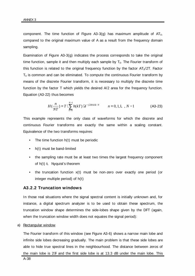
ANNEX 3
A-38
component. The time function of Figure A3-3(g) has maximum amplitude of AT0,
compared to the original maximum value of A as a result from the frequency domain
sampling.
Examination of Figure A3-3(g) indicates the process corresponds to take the original
time function, sample it and then multiply each sample by T0. The Fourier transform of
this function is related to the original frequency function by the factor AT0/2T. Factor
T0 is common and can be eliminated. To compute the continuous Fourier transform by
means of the discrete Fourier transform, it is necessary to multiply the discrete time
function by the factor T which yields the desired A/2 area for the frequency function.
Equation (A3-22) thus becomes
1,,1,0)()(1
0
/2 −=⋅⋅= ∑−
=
⋅⋅⋅⋅− NnekThTNTnH
N
k
Nknj Lπ (A3-23)
This example represents the only class of waveforms for which the discrete and
continuous Fourier transforms are exactly the same within a scaling constant.
Equivalence of the two transforms requires:
• The time function h(t) must be periodic
• h(t) must be band-limited
• the sampling rate must be at least two times the largest frequency component
of h(t) è Nyquist's theorem
• the truncation function x(t) must be non-zero over exactly one period (or
integer multiple period) of h(t)
A3.2.2 Truncation windows
In those real situations where the signal spectral content is initially unknown and, for
instance, a digital spectrum analyzer is to be used to obtain these spectrum, the
truncation window shape determines the side-lobes shape given by the DFT (again,
when the truncation window width does not equates the signal period):
a) Rectangular window
The Fourier transform of this window (see Figure A3-6) shows a narrow main lobe and
infinite side lobes decreasing gradually. The main problem is that these side lobes are
able to hide true spectral lines in the neighbourhood. The distance between zeros of
the main lobe is 2⋅F and the first side lobe is at 13.3 dB under the main lobe. This
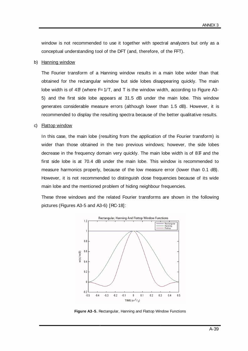
ANNEX 3
A-39
window is not recommended to use it together with spectral analyzers but only as a
conceptual understanding tool of the DFT (and, therefore, of the FFT).
b) Hanning window
The Fourier transform of a Hanning window results in a main lobe wider than that
obtained for the rectangular window but side lobes disappearing quickly. The main
lobe width is of 4⋅F (where F=1/T, and T is the window width, according to Figure A3-
5) and the first side lobe appears at 31.5 dB under the main lobe. This window
generates considerable measure errors (although lower than 1.5 dB). However, it is
recommended to display the resulting spectra because of the better qualitative results.
c) Flattop window
In this case, the main lobe (resulting from the application of the Fourier transform) is
wider than those obtained in the two previous windows; however, the side lobes
decrease in the frequency domain very quickly. The main lobe width is of 8⋅F and the
first side lobe is at 70.4 dB under the main lobe. This window is recommended to
measure harmonics properly, because of the low measure error (lower than 0.1 dB).
However, it is not recommended to distinguish close frequencies because of its wide
main lobe and the mentioned problem of hiding neighbour frequencies.
These three windows and the related Fourier transforms are shown in the following
pictures (Figures A3-5 and A3-6) [RC-18]:
Figure A3-5. Rectangular, Hanning and Flattop Window Functions
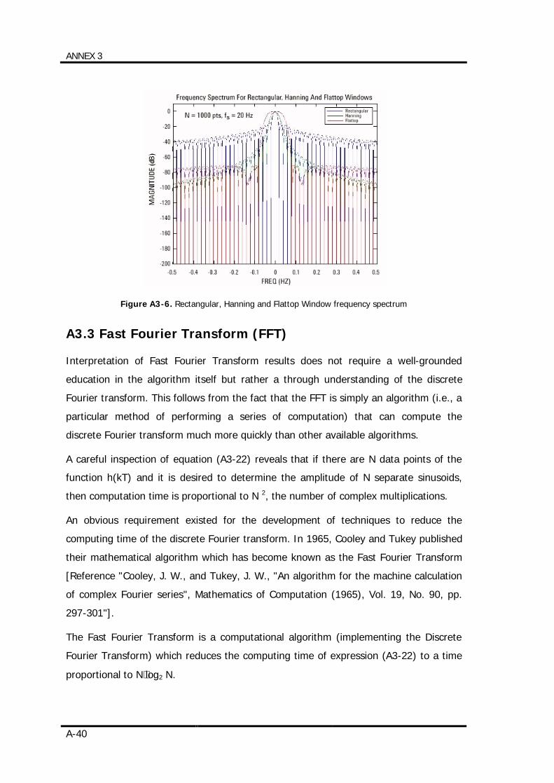
ANNEX 3
A-40
Figure A3-6. Rectangular, Hanning and Flattop Window frequency spectrum
A3.3 Fast Fourier Transform (FFT)
Interpretation of Fast Fourier Transform results does not require a well-grounded
education in the algorithm itself but rather a through understanding of the discrete
Fourier transform. This follows from the fact that the FFT is simply an algorithm (i.e., a
particular method of performing a series of computation) that can compute the
discrete Fourier transform much more quickly than other available algorithms.
A careful inspection of equation (A3-22) reveals that if there are N data points of the
function h(kT) and it is desired to determine the amplitude of N separate sinusoids,
then computation time is proportional to N 2, the number of complex multiplications.
An obvious requirement existed for the development of techniques to reduce the
computing time of the discrete Fourier transform. In 1965, Cooley and Tukey published
their mathematical algorithm which has become known as the Fast Fourier Transform
[Reference "Cooley, J. W., and Tukey, J. W., "An algorithm for the machine calculation
of complex Fourier series", Mathematics of Computation (1965), Vol. 19, No. 90, pp.
297-301"].
The Fast Fourier Transform is a computational algorithm (implementing the Discrete
Fourier Transform) which reduces the computing time of expression (A3-22) to a time
proportional to N⋅log2 N.

ANNEX 4
MATLAB ALGORITHM CODE LINES

ANNEX 4
A-43
ANNEX 4:
MATLAB ALGORITHM CODE LINES
% File name: SSCG.m % Creation date: 01.01.2001 % Last update date: 31.10.2003 % Comments: Frequency modulation of a sinusoidal waveform by using a selectable modulation profile. % Only symmetrical modulation around the carrier signal. % Note: Due to the selection of a complete period of the modulated signal (equal to 1/fm), no aliasing effect is present and, theferore, computed values match exactly the theoretical ones. % Preparing the workspace clear all; % Removes all variables, functions and MEX links from the
% current workspace clf reset; % Deletes everything and also resets all figure properties,
% except position, to their default values printyn = 1; % Control variable to plot modulation profile, its integral and
% the resulting frequency spectra: 1 = yes; 0 = no % 1.- Definitions and parameters fc = 1.2e+5; % Frequency (Hz) of the sinusoidal signal to be modulated
% (carrier waveform) fm = 1e+3; % Frequency (Hz) of the modulating signal Tc = 1/fc; % Period of the signal to be modulated Tm = 1/fm; % Period of the modulating signal % WARNING: So that the MATLAB function fft() works
% properly, the ratio fc/fm must be integer amp_c = 0.5; % Peak amplitude of the carrier signal (then,
% pk2pk=2*amp_m) expressed in volts. amp_m = 0.5; % Peak amplitude of the modulating signal (then,
% pk2pk=2*amp_m) expressed in volts. This value does not % take part directly in the calculation of the spectra; its true % influence is related to the algorithm through delta_fc (see % below), because Kw * amp_m = 2* pi * delta_fc (see % point 2.3.2). It is only intended for graphic representation % purposes.
pi = 3.1415926; s = 0.5; % Only for triangular modulation profile (see 2.3.2.2) for delta = 10:10 % deltaè percentage of modulation expressed in %,
% that is, delta = 10 means 10% (see point 2.1.1.2.1) % Some initializations vm = 0; % Initial value of the modulating waveform (see 2.3.2) theta = 0; % Initial value of the time-dependant angle (see 2.3.2) % Some necessary calculations if rem(fc,fm) > 0 % Because of the necessity of a ratio fc/fm integer fm = fc/(fix(fc/fm)+1) % we choose the nearest frequency fm towards zero

ANNEX 4
A-44
end % which makes fc/fm integer ratio=fc/fm % Just to check that fc/fm is integer Tm = 1 / fm; % A recalculation of Tm is mandatory, mainly if fm changed
delta_fc = delta/100*fc % Peak deviation of the carrier signal (see point 2.1.1.1) mf = delta_fc/fm % Modulation index (see 2.1.1.1) bandwidth = 2*delta_fc+2*fm; % Bandwidth of the spectra resulting from the modulation % (direct application of the Carson's rule) [see point 2.1.2] % Necessary to estimate the Nyquits's sampling frequency. % 2.- Process of calculation % 2.1.- Calculation of the number of points (power of 2) to compute the FFT fmax = fc+2.5*bandwidth % Maximum frequency to be found after modulation
% Because the Carson's bandwidth does not take into % account the whole spectra (only the 98% of the energy) % an extra range over this bandwidth is necessary.
fsampling = 2 * fmax % Direct expression of the Nyquist's theorem: the sampling % frequency must be at least twice the maximum frequency % of the original signal. p = fix(log2(fsampling/fm))+1 % Requirement of FFT is a number of points being a power
% of 2 N = 16*pow2(p) % Total number of samples to compute the FFT fsampling = fm * N % Final sampling frequency (actual) % 2.2. Selection of the modulating signal % opc = 1 Sinusoidal % opc = 2 Triangular % opc = 3 Exponential % opc = 4 Sampled modulation profile % opc = 5 Mixed (triangular + exponential) % opc = 6 Mixed (exponential + exponential) opc = 1; % Variable to select the modulation signal % 2.2.1.- Sinusoidal frequency modulation of a sinusoidal carrier (see 2.3.2.1) if opc == 1 % Sinusoidal modulation k = 1:N; % Although in 2.3.2.4, k = 0..N-1, for convenience a range
% from 1 to N is here selected
t = k*Tm/N; % Discretization in the time domain of the resulting % waveform period which is always Tm è sample spacing
vm = amp_m*sin(fm*t*2*pi); % Expression of the modulating waveform, only for % representation purposes
theta = mf * (1- cos(fm*t*2*pi)); % Integral of the modulating waveform f = amp_c*cos(fc*t*2*pi + theta); % Modulated waveform end if opc == 2 % Triangular modulation (see 2.3.2.2) for k=1:N % Although in 2.3.2.4, k = 0..N-1, for convenience a range

ANNEX 4
A-45
% from 1 to N is here selected t= k*Tm/N; % Discretization in the time domain of the resulting % waveform period which is always Tm è sample spacing if k <= s*N/2 vm(k)=2*amp_m*fm/s*t; % Expression of the modulating waveform theta(k)=2*pi*delta_fc*fm*t*t/s; % Integral of the modulating waveform elseif k > s*N/2 & k <= N*(1-s/2) vm(k)=amp_m/(1-s)*(1-2*fm*t); theta(k)=theta(s*N/2)+2*pi*delta_fc/(1-s)*(-fm*t*t+t+s/(2*fm)*(s/2-1)); % In order to use theta(s*N/2) this way, s must be % equal to 1/even_number elseif k > N*(1-s/2) & k <= N vm(k)=2*amp_m/s*(fm*t-1); theta(k)=theta(N*(1-s/2))+2*pi*delta_fc*1/s*(fm*t*t-2*t+(1-s*s/4)/fm); % In order to use theta(N*(1-s/2)) this way, s must be % equal to 1/even_number end f(k)=amp_c*cos(fc*t*2*pi + theta(k)); % Modulated waveform end end if opc == 3 % Exponential modulation (see 2.3.2.3) p=12*fm; % Parameter defining the curvature grade of the exponential R=1/(exp(p/(4*fm))-1); % Common factor to improve computing time for k=1:N % Although in 2.3.2.4, k = 0..N-1, for convenience a range
% from 1 to N is here selected t= k*Tm/N; % Discretization in the time domain of the resulting % waveform period which is always Tm è sample spacing if k <= N/4 vm(k) = amp_m*R*(exp(p*t)-1); % Expression of the modulating waveform
% Integral of the modulating waveform theta(k) = 2*pi*delta_fc*R/p*(exp(p*t)-p*t-1); elseif k > N/4 & k <= N/2 vm(k) = amp_m*R*(exp(p/(2*fm))*exp(-p*t)-1); theta(k) = theta (N/4)+2*pi*delta_fc*R/p*(-exp(-p*t)*exp(p/(2*fm))+exp(p/(4*fm))- p*t+p/(4*fm)); elseif k > N/2 & k <= 3*N/4 vm(k) = amp_m*R*(1-exp(-p/(2*fm))*exp(p*t)); theta(k) = theta(N/2)+2*pi*delta_fc*R/p*(-exp(p*t)*exp(-p/(2*fm))+p*t-p/(2*fm)+1); elseif k > 3*N/4 & k <= N vm(k) = amp_m*R*(1-exp(p/fm)*exp(-p*t)); theta(k) = theta(3*N/4)+2*pi*delta_fc*R/p*(exp(-p*t)*exp(p/fm)-exp(p/(4*fm))+p*t-3/4*p/fm); end vm(N) = 0; theta(N) = 0; f(k)=amp_c*cos(fc*t*2*pi + theta(k)); % Modulated waveform end end if opc == 4 % Sampled modulation profile (see 2.3.2.4)
ANNEX 4
A-46
% No offset considered load filename.txt % The file containing the discrete samples has the following vm = filename; % structure (text file, separators are feedlines): NP = filename (1); % first line: number of samples or points below (NP) i = 1:NP; % next lines: value (in volt) of the samples (vm) vm(i) = filename (i+1); suma_vm = vm(1); i = 1; theta(1) = 0; % Keep in mind that NP*∆T = N*∆TN = Tm and this is a for k=1:N % condition to produce the sample file t=(k-1)/(N*fm); if NP*(k-1) >= i*N; % and the reason for this inequality to work properly i = i +1; suma_vm = suma_vm + vm(i); theta(i) = 2*pi/NP/fm*(delta_fc * suma_vm); % Expression (2-117) in point 2.3.2.4 end f(k)=amp_c*cos(fc*t*2*pi + theta(i)); end end if opc == 5 % Mixed (triangular + exponential) p=12*fm; R=1/(exp(p/(4*fm))-1); for k=1:N t= k*Tm/N; if k <= N/4 vm(k) = amp_m*R*(exp(p*t)-1); theta(k) = 2*pi*delta_fc*R/p*(exp(p*t)-p*t-1); elseif k <= 3*N/4 vm(k)=2*amp_m*(1-2*fm*t); theta(k)=theta(N/4)+4*pi*delta_fc*(-fm*t*t+t-3/(16*fm)); elseif k <= N vm(k) = amp_m*R*(1-exp(p/fm)*exp(-p*t)); theta(k) = theta(3*N/4)+2*pi*delta_fc*R/p*(exp(-p*t)*exp(p/fm)-exp(p/(4*fm))+p*t-3/4*p/fm); end f(k)=amp_c*cos(fc*t*2*pi + theta(k)); end end if opc == 6 % Mixed (exponential + exponential) p=15*fm; R=1/(exp(p/(4*fm))-1); for k=1:N t= k*Tm/N; if k <= N/4 vm(k) = amp_m*R*(exp(p*t)-1); theta(k) = 2*pi*delta_fc*R/p*(exp(p*t)-p*t-1); elseif k > N/4 & k <= N/2 vm(k) = 1+amp_m*R*(1-exp(-p/(2*fm))*exp(p*t)); theta(k) = theta(N/4) + 2*pi*delta_fc*((t-Tm/4)*(1+R)-R/p*(exp(-p*Tm/4)*exp(p*t)-1)); elseif k > N/2 & k <= 3*N/4 vm(k) = amp_m*R*(exp(p*3/(4*fm))*exp(-p*t)-1)-1; theta(k) = theta(N/2) - 2*pi*delta_fc*(R/p*exp(p*Tm/4)*(exp(p*Tm/2)*exp(-p*t)-1)+(t- Tm/2)*(1+R)); elseif k > 3*N/4 & k <= N vm(k) = amp_m*R*(1-exp(p/fm)*exp(-p*t));
ANNEX 4
A-47
theta(k) = theta(3*N/4)+2*pi*delta_fc*R/p*(exp(-p*t)*exp(p/fm)-exp(p/(4*fm))+p*t-3/4*p/fm); end f(k)=amp_c*cos(fc*t*2*pi + theta(k)); end end % 2.3.- Calculation of the FFT Y = fft(f,N); Y = Y(1:1+N/2); % Only the 1 + N/2 first points contain the spectra
% information: % 1 is the dc component and 1+N/2, the Nyquist component % 2.4.- Graphical representation k=(0:N/2)*fm; f_ini = fc-1.0*bandwidth % Window of width (2*bandwidth) centered at fc to % display the significant spectra resulting from modulation f_fin = fc+1.0*bandwidth range = round(f_ini/fm:2+f_fin/fm); % Given the actual frequencies, vector points are calculated % by dividing them per fm. if printyn == 1 kk = (1:N)*Tm/N*1000; % Index related to the horizontal axis to be displayed % on the graphics. % Graphics of the modulating signal subplot(3,1,1),plot (kk,vm); grid zoom title ('Modulating waveform') xlabel ('time (ms)'); ylabel ('Amplitude (V)'); pause % Graphics of the modulating waveform integral subplot(3,1,2),plot (kk,theta); grid title ('Modulating waveform integral') xlabel ('time (ms)'); ylabel ('Angle (rad)'); pause % Graphics of the FFT MOD_FFT = 2/N*abs(Y(range))/sqrt(2); % Peak values of every side-band harmonic resulting from
% the modulation are simply calculated by multiplying the % module of the value given by the function FFT per 2/N
% Afterwards, divide the result per square root of 2 in order % to obtain the rms value (in volts). dBV = 20*log10(MOD_FFT); % Values in dBV (of a rms amplitude) subplot(3,1,3),bar (k(range)/1000,dBV) grid title ('After modulation')

ANNEX 4
A-48
xlabel ('Side-band harmonics (kHz)'); ylabel ('Amplitude (dBV)'); pause end end % Finally, some information must be saved into files. % Modulated signal (N samples). This file will be used later to be downloaded (after some % previous treatments) into the arbitrary function generator. fid = fopen ('C:\f_genert.txt', 'w'); fprintf (fid, '%12.8f \n', f); fclose (fid); % Significant spectral components values fid = fopen ('C:\f_spectr.txt', 'w'); fprintf (fid, '%6.2f %12.8f\n', [fm/1000*(range-1);MOD_FFT]); fclose (fid);
ANNEX 5
CONSIDERATIONS ABOUT EMC UNITS EXPRESSED IN
DECIBELS


ANNEX 5
A-51
ANNEX 5:
CONSIDERATIONS ABOUT EMC UNITS EXPRESSED IN DECIBELS
Decibels have the property of compressing data and other useful characteristics, as
expressing the gain or loss of a signal as a difference between the output signal and
the input signal. Although it is commonly referred as dB, some considerations must be
done in order to avoid a wrong usage of it.
Decibels are valid to express any ratio of two physical unit as volts, amperes, watts
and whichever combinations of them. EMC units are normally expressed this way:
− dB è it is a power reference
− dBV è With "V" at the end, this is a voltage reference.
− dBA è With "A" at the end, this is a current reference.
− and so on
1. BASIC DEFINITIONS
Commonest units in EMC expressed in decibels are watts and volts. As decibels are the
ratio of two quantities, absolute power, voltage or current levels are expressed in dB
by giving their value above or referenced to some base quantity. This way, some 'sub-
units' are used depending on the reference; for instance, a voltage referenced to 1 mV
will be expressed in dBmV, where the 'm' represents the 1mV-reference. More
examples are listed below:
POWER (W):
- dB è power referred to 1W è WWPdB⋅
⋅=1
)(log10 10
- dBm è power referred to 1mW è mWmWPdBm
⋅⋅=
1)(log10 10
- dBµ è power referred to 1µW è WWPdB
µµ
µ⋅
⋅=1
)(log10 10
RMS-VOLTAGES (V):
- dBV è voltage referred to 1VRMS è V
VVdBV RMS
⋅⋅=
1)(log20 10
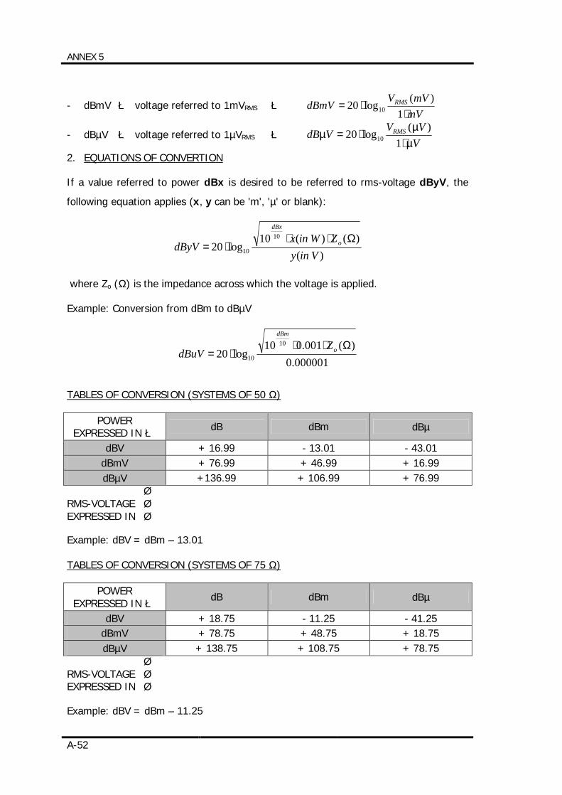
ANNEX 5
A-52
- dBmV è voltage referred to 1mVRMS è mV
mVVdBmV RMS
⋅⋅=
1)(log20 10
- dBµV è voltage referred to 1µVRMS è V
VVVdB RMS
µµ
µ⋅
⋅=1
)(log20 10
2. EQUATIONS OF CONVERTION
If a value referred to power dBx is desired to be referred to rms-voltage dByV, the
following equation applies (x, y can be 'm', 'µ' or blank):
)()()(10
log2010
10 VinyZWinx
dByV o
dBx
Ω⋅⋅⋅=
where Zo (Ω) is the impedance across which the voltage is applied.
Example: Conversion from dBm to dBµV
000001.0)(001.010
log2010
10
Ω⋅⋅⋅= o
dBm
ZdBuV
TABLES OF CONVERSION (SYSTEMS OF 50 Ω)
POWER EXPRESSED IN è dB dBm dBµ
dBV + 16.99 - 13.01 - 43.01 dBmV + 76.99 + 46.99 + 16.99 dBµV +136.99 + 106.99 + 76.99
é RMS-VOLTAGE é EXPRESSED IN é
Example: dBV = dBm – 13.01
TABLES OF CONVERSION (SYSTEMS OF 75 Ω)
POWER EXPRESSED IN è
dB dBm dBµ
dBV + 18.75 - 11.25 - 41.25 dBmV + 78.75 + 48.75 + 18.75 dBµV + 138.75 + 108.75 + 78.75
é RMS-VOLTAGE é EXPRESSED IN é
Example: dBV = dBm – 11.25
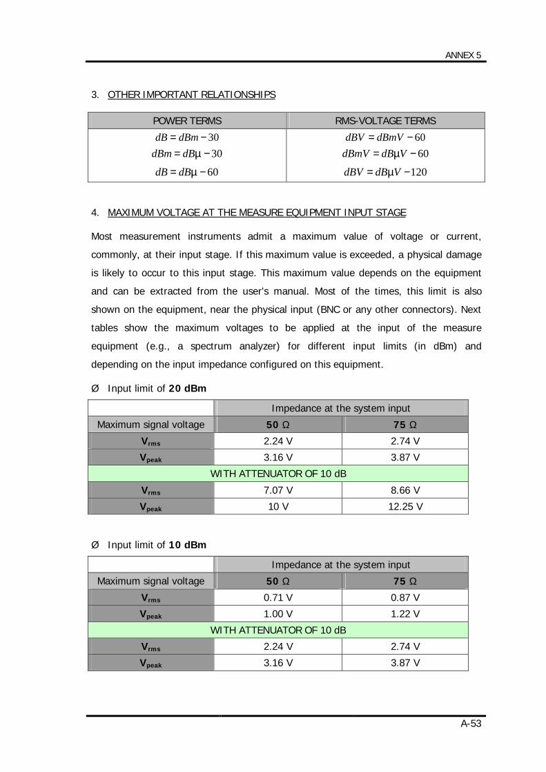
ANNEX 5
A-53
3. OTHER IMPORTANT RELATIONSHIPS
POWER TERMS RMS-VOLTAGE TERMS
30−= dBmdB
30−= µdBdBm
60−= µdBdB
60−= dBmVdBV
60−= VdBdBmV µ
120−= VdBdBV µ
4. MAXIMUM VOLTAGE AT THE MEASURE EQUIPMENT INPUT STAGE
Most measurement instruments admit a maximum value of voltage or current,
commonly, at their input stage. If this maximum value is exceeded, a physical damage
is likely to occur to this input stage. This maximum value depends on the equipment
and can be extracted from the user's manual. Most of the times, this limit is also
shown on the equipment, near the physical input (BNC or any other connectors). Next
tables show the maximum voltages to be applied at the input of the measure
equipment (e.g., a spectrum analyzer) for different input limits (in dBm) and
depending on the input impedance configured on this equipment.
Ø Input limit of 20 dBm
Impedance at the system input
Maximum signal voltage 50 Ω 75 Ω
Vrms 2.24 V 2.74 V
Vpeak 3.16 V 3.87 V
WITH ATTENUATOR OF 10 dB
Vrms 7.07 V 8.66 V
Vpeak 10 V 12.25 V
Ø Input limit of 10 dBm
Impedance at the system input
Maximum signal voltage 50 Ω 75 Ω
Vrms 0.71 V 0.87 V
Vpeak 1.00 V 1.22 V
WITH ATTENUATOR OF 10 dB
Vrms 2.24 V 2.74 V
Vpeak 3.16 V 3.87 V
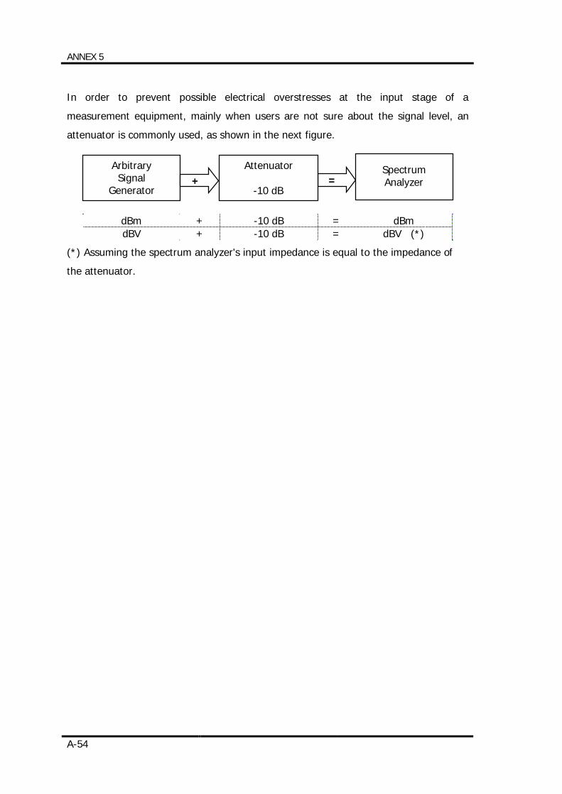
ANNEX 5
A-54
In order to prevent possible electrical overstresses at the input stage of a
measurement equipment, mainly when users are not sure about the signal level, an
attenuator is commonly used, as shown in the next figure.
dBm + -10 dB = dBm dBV + -10 dB = dBV (*)
(*) Assuming the spectrum analyzer's input impedance is equal to the impedance of
the attenuator.
Arbitrary Signal
Generator
Attenuator
-10 dB
Spectrum Analyzer
+ =

ANNEX 6
SCHEMATICS AND PCBs CORRESPONDING TO THE
TEST PLANT

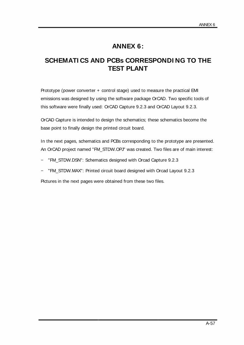
ANNEX 6
A-57
ANNEX 6:
SCHEMATICS AND PCBs CORRESPONDING TO THE TEST PLANT
Prototype (power converter + control stage) used to measure the practical EMI
emissions was designed by using the software package OrCAD. Two specific tools of
this software were finally used: OrCAD Capture 9.2.3 and OrCAD Layout 9.2.3.
OrCAD Capture is intended to design the schematics; these schematics become the
base point to finally design the printed circuit board.
In the next pages, schematics and PCBs corresponding to the prototype are presented.
An OrCAD project named "FM_STDW.OPJ" was created. Two files are of main interest:
− "FM_STDW.DSN": Schematics designed with Orcad Capture 9.2.3
− "FM_STDW.MAX": Printed circuit board designed with Orcad Layout 9.2.3
Pictures in the next pages were obtained from these two files.
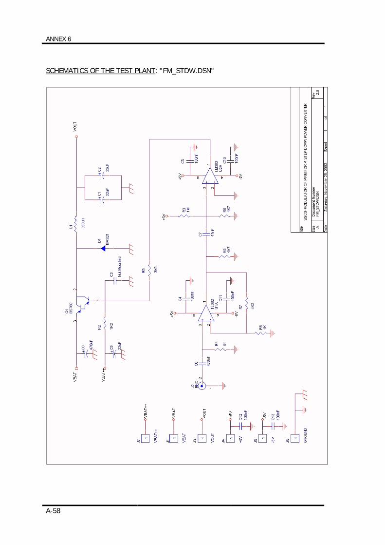
ANNEX 6
A-58
SCHEMATICS OF THE TEST PLANT: "FM_STDW.DSN"
ANNEX 6
A-59
PCB OF THE TEST PLANT: "FM_STDW.MAX"
§ TOP & BOTTOM LAYERS
TOP LAYER BOTTOM LAYER
§ COMPONENTS LAYOUT


ANNEX 7
PSPICE SIMULATION OF THE TEST PROTOTYPE

ANNEX 7
A-63
ANNEX 7:
PSPICE SIMULATION OF THE TEST PROTOTYPE
Test prototype presented in Annex 6 was previously simulated in order to estimate the
ability of this power converter to reach the higher level of frequency, around 1 MHz.
The software used to carry out this simulation was PSpice 9.2.3 (now included in the
OrCad software package).
In the two following two pages, simulations for both 1 MHz and 100 kHz are shown.
Components, their values and characteristics match exactly the ones presented in
Annex 6 (FM_STDW.DSN). The "Fm_stdw_schematic1.net" file with all interconnections
and component values is inserted at the end of this annex.
Three plots are displayed at each graph:
• V(Q1:c) è plot corresponding to the square waveform expected at the collector of
the power transistor Q1. Frequency and duty cycle values are numerically
presented.
• V(R5:2) è plot corresponding to the waveform at the output of the power
converter. Average value is numerically presented.
• V(L1:2) è plot corresponding to the waveform at the output of the amplification
stage, in order to show the equality between the input frequency from the signal
generator and the frequency generated by controlling the power transistor.
From the simulation results, it can be now concluded that no special problems should
be found in the practical test prototype.
The difference of duty-cycle values for the range 100 kHz to 1 MHz is lower than 14%,
thus expecting a ratio of variation for the duty-cycle around 1.55%/100 kHz. As an
example, for an input voltage of 10 V and a theoretical duty cycle of 50 %, the
variation of the output voltage for a frequency deviation of 100 kHz (δ% = 10 % and fc
= 1 MHz) is expected to be around 1.55%⋅10 V = 0.155 V ( about 3.1 % of the
theoretical output voltage of 5 V). Of course, practical results will differ from these
values (mainly due to the output capacitor) but they are good enough to continue.
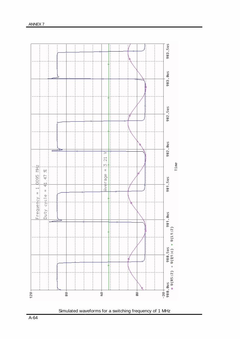
ANNEX 7
A-64
Simulated waveforms for a switching frequency of 1 MHz
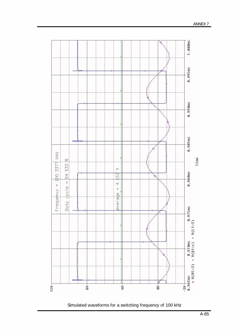
ANNEX 7
A-65
Simulated waveforms for a switching frequency of 100 kHz
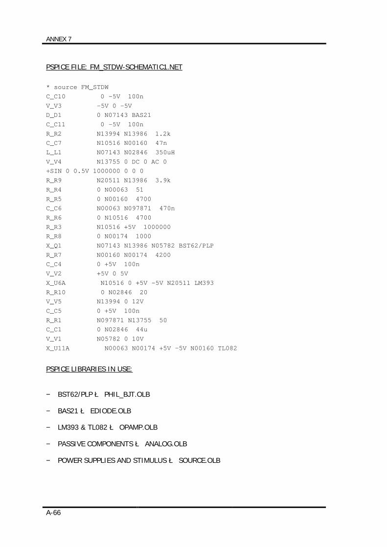
ANNEX 7
A-66
PSPICE FILE: FM_STDW-SCHEMATIC1.NET * source FM_STDW C_C10 0 -5V 100n V_V3 -5V 0 -5V D_D1 0 N07143 BAS21 C_C11 0 -5V 100n R_R2 N13994 N13986 1.2k C_C7 N10516 N00160 47n L_L1 N07143 N02846 350uH V_V4 N13755 0 DC 0 AC 0 +SIN 0 0.5V 1000000 0 0 0 R_R9 N20511 N13986 3.9k R_R4 0 N00063 51 R_R5 0 N00160 4700 C_C6 N00063 N097871 470n R_R6 0 N10516 4700 R_R3 N10516 +5V 1000000 R_R8 0 N00174 1000 X_Q1 N07143 N13986 N05782 BST62/PLP R_R7 N00160 N00174 4200 C_C4 0 +5V 100n V_V2 +5V 0 5V X_U6A N10516 0 +5V -5V N20511 LM393 R_R10 0 N02846 20 V_V5 N13994 0 12V C_C5 0 +5V 100n R_R1 N097871 N13755 50 C_C1 0 N02846 44u V_V1 N05782 0 10V X_U11A N00063 N00174 +5V -5V N00160 TL082
PSPICE LIBRARIES IN USE:
− BST62/PLP è PHIL_BJT.OLB
− BAS21 è EDIODE.OLB
− LM393 & TL082 è OPAMP.OLB
− PASSIVE COMPONENTS è ANALOG.OLB
− POWER SUPPLIES AND STIMULUS è SOURCE.OLB
Related Documents