AM3359, AM3358, AM3357 AM3356, AM3354, AM3352 www.ti.com SPRS717F – OCTOBER 2011 – REVISED APRIL 2013 Sitara™ AM335x ARM ® Cortex™-A8 Microprocessors (MPUs) Check for Samples: AM3359, AM3358 1 Device Summary 1.1 Features 1234567 – 32KB of L1 Data Cache with Single Error- • Highlights Detection (parity) – Up to 1-GHz Sitara™ ARM ® Cortex™-A8 – 256KB of L2 Cache with Error Correcting 32‑Bit RISC Microprocessor Code (ECC) • NEON™ SIMD Coprocessor – 176KB of On-Chip Boot ROM • 32KB of L1 Instruction and 32KB Data – 64KB of Dedicated RAM Cache with Single-Error Detection (parity) – Emulation and Debug • 256KB of L2 Cache with Error Correcting Code (ECC) • JTAG – mDDR(LPDDR), DDR2, DDR3, DDR3L – Interrupt Controller (up to 128 interrupt Support requests) – General-Purpose Memory Support (NAND, • On-Chip Memory (Shared L3 RAM) NOR, SRAM) Supporting Up to 16-bit ECC – 64 KB of General-Purpose On-Chip Memory – SGX530 3D Graphics Engine Controller (OCMC) RAM – LCD and Touchscreen Controller – Accessible to all Masters – Programmable Real-Time Unit and Industrial – Supports Retention for Fast Wake-Up Communication Subsystem (PRU-ICSS) • External Memory Interfaces (EMIF) – Real-Time Clock (RTC) – mDDR(LPDDR), DDR2, DDR3, DDR3L – Up to Two USB 2.0 High-Speed OTG Ports Controller: with Integrated PHY • mDDR: 200-MHz Clock (400-MHz Data – 10, 100, 1000 Ethernet Switch Supporting Up Rate) to Two Ports • DDR2: 266-MHz Clock (532-MHz Data – Serial Interfaces Including: Rate) • Two Controller Area Network Ports (CAN) • DDR3: 400-MHz Clock (800-MHz Data Rate) • Six UARTs, Two McASPs, Two McSPI, and Three I2C Ports • DDR3L: 400-MHz Clock (800-MHz Data Rate) – 12-Bit Successive Approximation Register (SAR) ADC • 16-Bit Data Bus – Up to Three 32-Bit Enhanced Capture • 1 GB of Total Addressable Space Modules (eCAP) • Supports One x16 or Two x8 Memory – Up to Three Enhanced High-Resolution PWM Device Configurations Modules (eHRPWM) – General-Purpose Memory Controller (GPMC) – Crypto Hardware Accelerators (AES, SHA, • Flexible 8-Bit and 16-Bit Asynchronous PKA, RNG) Memory Interface with Up to seven Chip Selects (NAND, NOR, Muxed-NOR, SRAM) • MPU Subsystem • Uses BCH Code to Support 4-Bit, 8-Bit, or 16-Bit ECC – Up to 1-GHz ARM ® Cortex™-A8 32-Bit RISC Microprocessor • Uses Hamming Code to Support 1-Bit ECC – NEON™ SIMD Coprocessor – Error Locator Module (ELM) – 32KB of L1 Instruction Cache with Single- Error Detection (parity) • Used in Conjunction with the GPMC to 1 Please be aware that an important notice concerning availability, standard warranty, and use in critical applications of Texas Instruments semiconductor products and disclaimers thereto appears at the end of this data sheet. 2Sitara, SmartReflex, DSP/BIOS, XDS are trademarks of Texas Instruments. 3Cortex, NEON are trademarks of ARM Ltd or its subsidiaries. 4ARM is a registered trademark of ARM Ltd or its subsidiaries. 5EtherCAT is a registered trademark of EtherCAT Technology Group. 6POWERVR SGX is a trademark of Imagination Technologies Limited. 7All other trademarks are the property of their respective owners. PRODUCTION DATA information is current as of publication date. Products conform to Copyright © 2011–2013, Texas Instruments Incorporated specifications per the terms of the Texas Instruments standard warranty. Production processing does not necessarily include testing of all parameters.

Welcome message from author
This document is posted to help you gain knowledge. Please leave a comment to let me know what you think about it! Share it to your friends and learn new things together.
Transcript

AM3359, AM3358, AM3357AM3356, AM3354, AM3352
www.ti.com SPRS717F –OCTOBER 2011–REVISED APRIL 2013
Sitara™ AM335x ARM® Cortex™-A8 Microprocessors (MPUs)Check for Samples: AM3359, AM3358
1 Device Summary
1.1 Features1234567
– 32KB of L1 Data Cache with Single Error-• HighlightsDetection (parity)– Up to 1-GHz Sitara™ ARM® Cortex™-A8
– 256KB of L2 Cache with Error Correcting32‑‑Bit RISC MicroprocessorCode (ECC)• NEON™ SIMD Coprocessor
– 176KB of On-Chip Boot ROM• 32KB of L1 Instruction and 32KB Data– 64KB of Dedicated RAMCache with Single-Error Detection (parity)– Emulation and Debug• 256KB of L2 Cache with Error Correcting
Code (ECC) • JTAG– mDDR(LPDDR), DDR2, DDR3, DDR3L – Interrupt Controller (up to 128 interrupt
Support requests)– General-Purpose Memory Support (NAND, • On-Chip Memory (Shared L3 RAM)
NOR, SRAM) Supporting Up to 16-bit ECC – 64 KB of General-Purpose On-Chip Memory– SGX530 3D Graphics Engine Controller (OCMC) RAM– LCD and Touchscreen Controller – Accessible to all Masters– Programmable Real-Time Unit and Industrial – Supports Retention for Fast Wake-Up
Communication Subsystem (PRU-ICSS) • External Memory Interfaces (EMIF)– Real-Time Clock (RTC) – mDDR(LPDDR), DDR2, DDR3, DDR3L– Up to Two USB 2.0 High-Speed OTG Ports Controller:
with Integrated PHY • mDDR: 200-MHz Clock (400-MHz Data– 10, 100, 1000 Ethernet Switch Supporting Up Rate)
to Two Ports • DDR2: 266-MHz Clock (532-MHz Data– Serial Interfaces Including: Rate)
• Two Controller Area Network Ports (CAN) • DDR3: 400-MHz Clock (800-MHz DataRate)• Six UARTs, Two McASPs, Two McSPI,
and Three I2C Ports • DDR3L: 400-MHz Clock (800-MHz DataRate)– 12-Bit Successive Approximation Register
(SAR) ADC • 16-Bit Data Bus– Up to Three 32-Bit Enhanced Capture • 1 GB of Total Addressable Space
Modules (eCAP) • Supports One x16 or Two x8 Memory– Up to Three Enhanced High-Resolution PWM Device Configurations
Modules (eHRPWM) – General-Purpose Memory Controller (GPMC)– Crypto Hardware Accelerators (AES, SHA, • Flexible 8-Bit and 16-Bit Asynchronous
PKA, RNG) Memory Interface with Up to seven ChipSelects (NAND, NOR, Muxed-NOR, SRAM)
• MPU Subsystem • Uses BCH Code to Support 4-Bit, 8-Bit, or16-Bit ECC– Up to 1-GHz ARM® Cortex™-A8 32-Bit RISC
Microprocessor • Uses Hamming Code to Support 1-BitECC– NEON™ SIMD Coprocessor
– Error Locator Module (ELM)– 32KB of L1 Instruction Cache with Single-Error Detection (parity) • Used in Conjunction with the GPMC to
1
Please be aware that an important notice concerning availability, standard warranty, and use in critical applications ofTexas Instruments semiconductor products and disclaimers thereto appears at the end of this data sheet.
2Sitara, SmartReflex, DSP/BIOS, XDS are trademarks of Texas Instruments.3Cortex, NEON are trademarks of ARM Ltd or its subsidiaries.4ARM is a registered trademark of ARM Ltd or its subsidiaries.5EtherCAT is a registered trademark of EtherCAT Technology Group.6POWERVR SGX is a trademark of Imagination Technologies Limited.7All other trademarks are the property of their respective owners.
PRODUCTION DATA information is current as of publication date. Products conform to Copyright © 2011–2013, Texas Instruments Incorporatedspecifications per the terms of the Texas Instruments standard warranty. Productionprocessing does not necessarily include testing of all parameters.
AM3359, AM3358, AM3357AM3356, AM3354, AM3352
SPRS717F –OCTOBER 2011–REVISED APRIL 2013 www.ti.com
Locate Addresses of Data Errors from Week) and Time (Hours-Minutes-Seconds)Syndrome Polynomials Generated Using Informationa BCH Algorithm – Internal 32.768-kHz Oscillator, RTC Logic
• Supports 4-Bit, 8-Bit, and 16-Bit per 512- and 1.1-V Internal LDObyte Block Error Location Based on BCH – Independent Power-on-ResetAlgorithms (RTC_PWRONRSTn) Input
• Programmable Real-Time Unit and Industrial – Dedicated Input Pin (EXT_WAKEUP) forCommunication Subsystem (PRU-ICSS) External Wake Events– Supports protocols such as EtherCAT®, – Programmable Alarm Can be Used to
PROFIBUS, PROFINET, EtherNet/IP™, and Generate Internal Interrupts to the PRCM (formore Wake Up) or Cortex-A8 (for Event
– Peripherals Inside the PRU-ICSS Notification)• One UART Port with Flow Control Pins, – Programmable Alarm Can be Used with
Supports Up to 12 Mbps External Output (PMIC_POWER_EN) toEnable the Power Management IC to Restore• Two MII Ethernet Ports that SupportNon-RTC Power DomainsIndustrial Ethernet, such as EtherCAT
• Peripherals• One MDIO Port– Up to Two USB 2.0 High-Speed OTG Ports• One Enhanced Capture (eCAP) Module
with Integrated PHY• Power Reset and Clock Management (PRCM)– Up to Two Industrial Gigabit Ethernet MACsModule
(10, 100, 1000 Mbps)– Controls the entry and Exit of Stand-By and• Integrated SwitchDeep-Sleep Modes• Each MAC Supports MII, RMII, RGMII and– Responsible for Sleep Sequencing, Power
MDIO InterfacesDomain Switch-Off Sequencing, Wake-UpSequencing and Power Domain Switch-On • Ethernet MACs and Switch Can OperateSequencing Independent of Other Functions
– Clocks • IEEE 1588v2 Precision Time Protocol(PTP)• Integrated 15-35 MHz High-Frequency
Oscillator Used to Generate a Reference – Up to Two Controller-Area Network (CAN)Clock for Various System and Peripheral PortsClocks • Supports CAN Version 2 Parts A and B
• Supports Individual Clock Enable and – Up to Two Multichannel Audio Serial PortsDisable Control for Subsystems and (McASP)Peripherals to Facilitate Reduced Power • Transmit and Receive Clocks Up to 50Consumption MHz
• Five ADPLLs to Generate System Clocks • Up to Four Serial Data Pins per McASP(MPU Subsystem, DDR Interface, USB Port with Independent TX and RX Clocksand Peripherals [MMC and SD, UART, • Supports Time Division MultiplexingSPI, I2C], L3, L4, Ethernet, GFX [SGX530], (TDM), Inter-IC Sound (I2S), and similarLCD Pixel Clock) Formats
– Power • Supports Digital Audio Interface• Two Non-Switchable Power Domains Transmission (SPDIF, IEC60958-1, and
(Real-Time Clock [RTC], Wake-Up Logic AES-3 Formats)[WAKE-UP]) • FIFO Buffers for Transmit and Receive
• Three Switchable Power Domains (MPU (256 bytes)Subsystem [MPU], SGX530 [GFX], – Up to Six UARTsPeripherals and Infrastructure [PER])
• All UARTs Support IrDA and CIR Modes• Implements SmartReflex™ Class 2B for• All UARTs Support RTS and CTS FlowCore Voltage Scaling Based On Die
ControlTemperature, Process Variation and• UART1 Supports Full Modem controlPerformance (Adaptive Voltage Scaling
– Up to Two Master and Slave McSPI Serial[AVS])Interfaces• Dynamic Voltage Frequency Scaling• Up to Two Chip Selects(DVFS)• Up to 48 MHz• Real-Time Clock (RTC)
– Up to Three MMC, SD, and SDIO Ports– Real-Time Date (Day-Month-Year-Day of
2 Device Summary Copyright © 2011–2013, Texas Instruments Incorporated
Submit Documentation FeedbackProduct Folder Links: AM3359 AM3358 AM3357 AM3356 AM3354 AM3352
AM3359, AM3358, AM3357AM3356, AM3354, AM3352
www.ti.com SPRS717F –OCTOBER 2011–REVISED APRIL 2013
• 1-Bit, 4-Bit and 8-Bit MMC, SD, and SDIO a Firmware TimerModes • 512-Word Deep Internal FIFO
• MMCSD0 has dedicated Power Rail for • Supported Display Types:1.8-V or 3.3-V Operation – Character Displays - Uses LCD
• Up to 48-MHz Data Transfer Rate Interface Display Driver (LIDD)• Supports Card Detect and Write Protect Controller to Program these Displays• Complies with MMC4.3 and SD and SDIO – Passive Matrix LCD Displays - Uses
2.0 Specifications LCD Raster Display Controller toProvide Timing and Data for Constant– Up to Three I2C Master and Slave InterfacesGraphics Refresh to a Passive Display• Standard Mode (up to 100 kHz)
– Active Matrix LCD Displays - Uses• Fast Mode (up to 400 kHz)External Frame Buffer Space and the– Up to Four Banks of General-Purpose IO Internal DMA Engine to Drive(GPIO) Streaming Data to the Panel
• 32 GPIOs per Bank (Multiplexed with – 12-Bit Successive Approximation RegisterOther Functional Pins) (SAR) ADC• GPIOs Can be Used as Interrupt Inputs • 200K Samples per Second(Up to Two Interrupt Inputs per Bank)
• Input Can be Selected from any of the– Up to Three External DMA Event Inputs That Eight Analog Inputs Multiplexed ThroughCan Also be Used as Interrupt Inputs an 8:1 analog Switch– Eight 32-Bit General-Purpose Timers • Can be Configured to Operate as a 4-wire,
• DMTIMER1 is a 1-ms Timer Used for 5-wire, or 8-wire Resistive Touch ScreenOperating System (OS) Ticks Controller (TSC) Interface
• DMTIMER4 - DMTIMER7 are Pinned Out – Up to Three 32-Bit Enhanced Capture– One Watchdog Timer Modules (eCAP)– SGX530 3D Graphics Engine • Configurable as Three Capture Inputs or
• Tile-Based Architecture Delivering Up to Three Auxiliary PWM Outputs20 Million Polygons per second – Up to Three Enhanced High-Resolution PWM
• Universal Scalable Shader Engine is a Modules (eHRPWM)Multi-Threaded Engine Incorporating • Dedicated 16-Bit Time-Base Counter withPixel and Vertex Shader Functionality Time and Frequency Controls
• Advanced Shader Feature Set in Excess • Configurable as Six Single-Ended, Sixof Microsoft VS3.0, PS3.0 and OGL2.0 Dual-Edge Symmetric, or Three Dual-
• Industry Standard API Support of Edge Asymmetric OutputsDirect3D Mobile, OGL-ES 1.1 and 2.0, – Up to Three 32-Bit Enhanced QuadratureOpenVG 1.0, and OpenMax Encoder Pulse (eQEP) Modules
• Fine-Grained Task Switching, Load • Device IdentificationBalancing and Power Management – Contains Electrical fuse Farm (FuseFarm) of
• Advanced Geometry DMA Driven Which Some Bits are Factory ProgrammableOperation for Minimum CPU Interaction • Production ID
• Programmable High-Quality Image Anti- • Device Part Number (Unique JTAG ID)Aliasing • Device Revision (readable by Host ARM)
• Fully Virtualized Memory Addressing for • Debug Interface SupportOS Operation in a Unified Memory– JTAG and cJTAG for ARM (Cortex-A8 andArchitecture
PRCM), PRU-ICSS Debug– LCD Controller– Supports Device Boundary Scan• Up to 24-Bits Data Output; 8-Bits per– Supports IEEE 1500Pixel (RGB)
• DMA• Resolution Up to 2048x2048 (With– On-Chip Enhanced DMA Controller (EDMA)Maximum 126-MHz Pixel Clock)
has Three Third-Party Transfer Controllers• Integrated LCD Interface Display Driver(TPTC) and One Third-Party Channel(LIDD) ControllerController (TPCC), Which Supports Up to 64• Integrated Raster Controller Programmable Logical Channels and Eight
• Integrated DMA Engine to Pull Data from QDMA Channels. EDMA is Used for:the External Frame Buffer without • Transfers to and from On-Chip MemoriesBurdening the Processor via Interrupts or
Copyright © 2011–2013, Texas Instruments Incorporated Device Summary 3Submit Documentation Feedback
Product Folder Links: AM3359 AM3358 AM3357 AM3356 AM3354 AM3352
AM3359, AM3358, AM3357AM3356, AM3354, AM3352
SPRS717F –OCTOBER 2011–REVISED APRIL 2013 www.ti.com
• Transfers to and from External Storage • Security(EMIF, General-Purpose Memory – Crypto Hardware Accelerators (AES, SHA,Controller, Slave Peripherals) PKA, RNG)
• Inter-Processor Communication (IPC) • Boot Modes– Integrates Hardware-Based Mailbox for IPC – Boot Mode is Selected via Boot
and Spinlock for Process Synchronization Configuration Pins Latched on the RisingBetween the Cortex-A8, PRCM, and PRU- Edge of the PWRONRSTn Reset Input PinICSS • Packages:• Mailbox Registers that Generate – 298-Pin S-PBGA-N298 Via Channel™
Interrupts package– Four Initiators (Cortex-A8, PRCM, (ZCE Suffix), 0.65-mm Ball Pitch
PRU0, PRU1) – 324-Pin S-PBGA-N324 package• Spinlock has 128 Software-Assigned (ZCZ Suffix), 0.80-mm Ball Pitch
Lock Registers
1.2 Applications• Gaming Peripherals • Connected Vending Machines• Home and Industrial Automation • Weighing Scales• Consumer Medical Appliances • Educational Consoles• Printers • Advanced Toys• Smart Toll Systems
4 Device Summary Copyright © 2011–2013, Texas Instruments Incorporated
Submit Documentation FeedbackProduct Folder Links: AM3359 AM3358 AM3357 AM3356 AM3354 AM3352

AM3359, AM3358, AM3357AM3356, AM3354, AM3352
www.ti.com SPRS717F –OCTOBER 2011–REVISED APRIL 2013
1.3 Description
The AM335x microprocessors, based on the ARM Cortex-A8, are enhanced with image, graphicsprocessing, peripherals and industrial interface options such as EtherCAT and PROFIBUS. The devicesupports the following high-level operating systems (HLOSs) that are available free of charge from TI:• Linux®
• Android™
The AM335x microprocessor contains these subsystems:• Microprocessor unit (MPU) subsystem based on the ARM Cortex-A8 microprocessor.• POWERVR SGX™ Graphics Accelerator subsystem for 3D graphics acceleration to support display
and gaming effects.• The Programmable Real-Time Unit and Industrial Communication Subsystem (PRU-ICSS) is separate
from the ARM core, allowing independent operation and clocking for greater efficiency and flexibility.The PRU-ICSS enables additional peripheral interfaces and real-time protocols such as EtherCAT,PROFINET, EtherNet/IP, PROFIBUS, Ethernet Powerlink, Sercos, and others.
Copyright © 2011–2013, Texas Instruments Incorporated Device Summary 5Submit Documentation Feedback
Product Folder Links: AM3359 AM3358 AM3357 AM3356 AM3354 AM3352
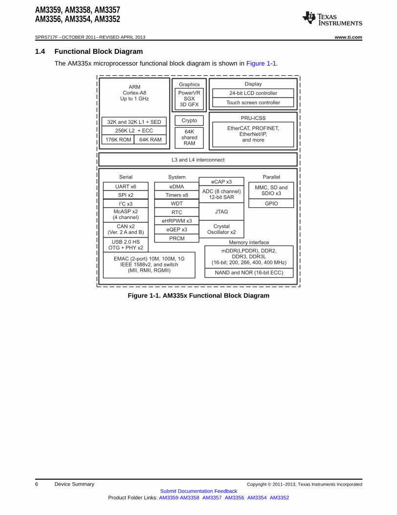
ARMCortex-A8
Up to 1 GHz
32K and 32K L1 + SED
256K L2 + ECC
176K ROM 64K RAM
Graphics
PowerVRSGX
3D GFX
Crypto
64KsharedRAM
24-bit LCD controller
Touch screen controller
Display
PRU-ICSS
EtherCAT, PROFINET,EtherNet/IP,and more
L3 and L4 interconnect
USB 2.0 HSOTG + PHY x2
CAN x2(Ver. 2 A and B)
McASP x2(4 channel)
I C x32
SPI x2
UART x6
Serial System Parallel
eDMA
Timers x8
WDT
RTC
eHRPWM x3
eQEP x3
PRCM
eCAP x3
ADC (8 channel)12-bit SAR
JTAG
CrystalOscillator x2
MMC, SD andSDIO x3
GPIO
EMAC (2-port) 10M, 100M, 1GIEEE 1588v2, and switch
(MII, RMII, RGMII)
mDDR(LPDDR), DDR2,DDR3, DDR3L
(16-bit; 200, 266, 400, 400 MHz)
NAND and NOR (16-bit ECC)
Memory interface
AM3359, AM3358, AM3357AM3356, AM3354, AM3352
SPRS717F –OCTOBER 2011–REVISED APRIL 2013 www.ti.com
1.4 Functional Block Diagram
The AM335x microprocessor functional block diagram is shown in Figure 1-1.
Figure 1-1. AM335x Functional Block Diagram
6 Device Summary Copyright © 2011–2013, Texas Instruments Incorporated
Submit Documentation FeedbackProduct Folder Links: AM3359 AM3358 AM3357 AM3356 AM3354 AM3352
AM3359, AM3358, AM3357AM3356, AM3354, AM3352
www.ti.com SPRS717F –OCTOBER 2011–REVISED APRIL 2013
5.2 Recommended Clock and Control Signal Transition1 Device Summary ........................................ 1Behavior ........................................... 1151.1 Features ............................................. 1
5.3 Controller Area Network (CAN) ................... 1161.2 Applications .......................................... 45.4 DMTimer .......................................... 1171.3 Description ........................................... 55.5 Ethernet Media Access Controller (EMAC) and1.4 Functional Block Diagram ........................... 6
Switch ............................................. 118Revision History .............................................. 8
5.6 External Memory Interfaces ....................... 1262 Terminal Description .................................. 10
5.7 Inter-Integrated Circuit (I2C) ...................... 1892.1 Pin Assignments .................................... 10
5.8 JTAG Electrical Data and Timing ................. 1912.2 Ball Characteristics ................................. 18
5.9 LCD Controller (LCDC) ............................ 1922.3 Signal Description .................................. 51
5.10 Multichannel Audio Serial Port (McASP) .......... 2083 Device Operating Conditions ....................... 80
5.11 Multichannel Serial Port Interface (McSPI) ....... 2133.1 Absolute Maximum Ratings ........................ 80
5.12 Multimedia Card (MMC) Interface ................. 2193.2 Recommended Operating Conditions .............. 82 5.13 Universal Asynchronous Receiver Transmitter3.3 DC Electrical Characteristics ....................... 90 (UART) ............................................ 2223.4 External Capacitors ................................. 94 6 Device and Documentation Support ............. 2253.5 Touchscreen Controller and Analog-to-Digital 6.1 Device Support .................................... 225
Subsystem Electrical Parameters .................. 976.2 Documentation Support ........................... 226
4 Power and Clocking ................................... 997 Mechanical Packaging and Orderable
4.1 Power Supplies ..................................... 99 Information ............................................ 2284.2 Clock Specifications ............................... 106 7.1 Thermal Data for ZCE and ZCZ Packages ....... 228
5 Peripheral Information and Timings ............. 115 7.2 Via Channel ....................................... 2285.1 Parameter Information ............................ 115 7.3 Packaging Information ............................ 228
Copyright © 2011–2013, Texas Instruments Incorporated Contents 7Submit Documentation Feedback
Product Folder Links: AM3359 AM3358 AM3357 AM3356 AM3354 AM3352

AM3359, AM3358, AM3357AM3356, AM3354, AM3352
SPRS717F –OCTOBER 2011–REVISED APRIL 2013 www.ti.com
Revision HistoryNOTE: Page numbers for previous revisions may differ from page numbers in the current version.
Changes from Revision E (January 2013) to Revision F Page
• Changed device status to Production Data ....................................................................................... 1• Changed ARM speeds features list item .......................................................................................... 1• Changed MPU Subsystem speeds features list item ........................................................................... 1• Changed Features list item for DDR3 ............................................................................................. 1• Changed Features list item for DDR3L ........................................................................................... 1• Changed Figure 1-1, AM335x Functional Block Diagram ...................................................................... 6• Changed Type value to I for Mode 2 (uart5_rxd) in Table 2-7, Ball Characteristics (ZCE and ZCZ Packages) ....... 37• Added Footnote (3) in Table 2-7, Ball Characteristics (ZCE and ZCZ Packages) ......................................... 49• Changed Footnote (4) in Table 2-7, Ball Characteristics (ZCE and ZCZ Packages) ...................................... 49• Added RTC_PORz Signal Name to Table 2-17, Miscellaneous/Miscellaneous Signals Description .................... 60• Deleted ESD-CDM (Charged-Device Model) Corner Terminals Parameter and changed MIN value for Latch-up
Performance Parameter in Table 3-1 ............................................................................................ 80• Changed DDR3, DDR3L value for OPP100 and deleted Footnote (3) in Table 3-2, VDD_CORE Operating
Performance Points for ZCZ Package with Device Revision Code "Blank" ................................................ 82• Deleted OPP50 row from Table 3-3, VDD_MPU Operating Performance Points for ZCZ Package with Device
Revision Code "Blank" ............................................................................................................. 82• Added Table 3-4, Valid Combinations of VDD_CORE and VDD_MPU Operating Performance Points for ZCZ
Package with Device Revision Code "Blank" ................................................................................... 82• Changed DDR3, DDR3L value for OPP100, deleted Footnote (4) and deleted OPP50 row from Table 3-5,
VDD_CORE Operating Performance Points for ZCE Package with Device Revision Code "Blank" .................... 83• Changed DDR3, DDR3L value for OPP100 and deleted Footnote (3) in Table 3-6, VDD_CORE Operating
Performance Points for ZCZ Package with Device Revision Code "A" or Newer ......................................... 84• Changed Table 3-7, VDD_MPU Operating Performance Points for ZCZ Package with Device Revision Code "A"
or Newer ............................................................................................................................. 84• Added Table 3-8, Valid Combinations of VDD_CORE and VDD_MPU Operating Performance Points for ZCZ
Package with Device Revision Code "A" or Newer ............................................................................ 84• Changed DDR3, DDR3L value for OPP100 and deleted Footnote (4) in Table 3-9, VDD_CORE Operating
Performance Points for ZCE Package with Device Revision Code "A" or Newer ......................................... 85• Added VDD_MPU Nitro Description and MAX value in Table 3-10, Maximum Current Ratings at AM335x Power
Terminals ............................................................................................................................ 86• Changed MAX value for VDDS_DDR Supply in Table 3-10, Maximum Current Ratings at AM335x Power
Terminals ............................................................................................................................ 86• Added paragraphs in the POH section before and after Table 3-11, Reliability Data ..................................... 87• Added Operating Condition Nitro to Table 3-11, Reliability Data ............................................................ 87• Added MIN, NOM, and MAX for VDD_MPU Nitro mode; deleted values from USB0_ID and USB1_ID; added
Footnote (7) in Table 3-12, Recommended Operating Conditions .......................................................... 87• Changed VOH, VOL, II and IOZ Parameter values in Table 3-13, DC Electrical Characteristics Over Recommended
Ranges of Supply Voltage and Operating Temperature ...................................................................... 90• Deleted TYP value for CVDDS_DDR Parameter in Table 3-15, Power-Supply Decoupling Capacitor Characteristics ... 94• Changed second paragraph in Section 4.2.2.3, OSC1 Internal Oscillator Clock Source ............................... 110• Changed second paragraph in Section 4.2.2.4, OSC1 LVCMOS Digital Clock Source ................................. 112• Added Section 5.4, DMTimer .................................................................................................... 117• Added OPP50 MIN values for all parameters and changed OPP100 MIN value for Parameters F13 and F22 in
Table 5-21, GPMC and NOR Flash Timing Requirements—Synchronous Mode ........................................ 126• Added OPP50 MIN and MAX values and changed MIN values of OPP100 Parameters F7 and F8 in Table 5-22,
GPMC and NOR Flash Switching Characteristics—Synchronous Mode .................................................. 127• Changed OPP50 MIN and MAX Parameter values in Table 5-26, GPMC and NOR Flash Switching
Characteristics—Asynchronous Mode ......................................................................................... 136• Changed OPP50 MIN and MAX Parameter values in Table 5-30, GPMC and NAND Flash Switching
Characteristics—Asynchronous Mode ......................................................................................... 145• Changed MIN value for Parameter 1 in Table 5-56, Switching Characteristics for DDR3 Memory Interface ........ 170• Added Conditions to Parameter 1 and deleted Footnote in Table 5-58, Compatible JEDEC DDR3 Devices (Per
Interface) ........................................................................................................................... 174• Changed Footnote (12) in Table 5-66, CK and ADDR_CTRL Routing Specification .................................... 187• Changed Footnote (11) in Table 5-67, DQS[x] and DQ[x] Routing Specification ........................................ 188
8 Contents Copyright © 2011–2013, Texas Instruments Incorporated
Submit Documentation FeedbackProduct Folder Links: AM3359 AM3358 AM3357 AM3356 AM3354 AM3352

AM3359, AM3358, AM3357AM3356, AM3354, AM3352
www.ti.com SPRS717F –OCTOBER 2011–REVISED APRIL 2013
• Deleted MIN values for Parameters 9-12 in Table 5-69, Timing Requirements for I2C Input Timings ................ 189• Added Section 5.8, JTAG Electrical Data and Timing ....................................................................... 191• Changed MIN values of Parameters 5, 6, 8, and 10 and MAX values of Parameters 4, 6, 8, and 10 in Table 5-
76, Switching Characteristics for LCD Raster Mode ......................................................................... 202• Added OPP50 MIN and MAX Parameter values and changed OPP100 Parameters 6 and 8 MIN values in
Table 5-78, Timing Requirements for McASP ................................................................................ 209• Added OPP50 MIN and MAX Parameter values and changed OPP100 Parameters 13, 14 and 15 MIN values in
Table 5-79, Switching Characteristics for McASP ............................................................................ 211• Added OPP50 MIN and MAX Parameter values to Table 5-81, Timing Requirements for McSPI Input
Timings—Slave Mode ............................................................................................................ 213• Added OPP50 MIN and MAX Parameter values to Table 5-82, Switching Characteristics for McSPI Output
Timings—Slave Mode ............................................................................................................ 213• Changed Input Parameters High Load MAX values in Table 5-83, McSPI Timing Conditions—Master Mode ...... 216• Added OPP50 MIN and MAX Parameter values and changed OPP100 Parameter 5 MIN values in Table 5-84,
Timing Requirements for McSPI Input Timings—Master Mode ............................................................ 216• Added OPP50 MIN and MAX Parameter values and changed OPP100 Parameters 2 and 3 MAX values in
Table 5-85, Switching Characteristics for McSPI Output Timings—Master Mode ....................................... 216• Changed MIN value for Parameters 2 and 4 in Table 5-87, Timing Requirements for MMC[x]_CMD and
MMC[x]_DAT[7:0] ................................................................................................................. 219• Added OPP50 MIN, TYP, and MAX Parameter values to Table 5-89, Switching Characteristics for MMC[x]_CMD
and MMC[x]_DAT[7:0]—Standard Mode ...................................................................................... 220• Added OPP50 MIN, TYP, and MAX Parameter values to Table 5-90, Switching Characteristics for MMC[x]_CMD
and MMC[x]_DAT[7:0]—High-Speed Mode ................................................................................... 221• Changed Figure 6-1, AM335x Device Nomenclature ........................................................................ 226• Added paragraph to Section 7.1, Thermal Data for ZCE and ZCZ Packages ............................................ 228
Copyright © 2011–2013, Texas Instruments Incorporated Contents 9Submit Documentation Feedback
Product Folder Links: AM3359 AM3358 AM3357 AM3356 AM3354 AM3352

AM3359, AM3358, AM3357AM3356, AM3354, AM3352
SPRS717F –OCTOBER 2011–REVISED APRIL 2013 www.ti.com
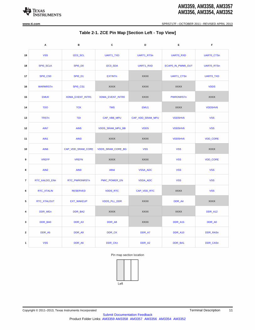
2 Terminal Description
2.1 Pin Assignments
NOTEThe terms "ball", "pin", and "terminal" are used interchangeably throughout the document. Anattempt is made to use "ball" only when referring to the physical package.
2.1.1 ZCE Package Pin Maps (Top View)
The pin maps below show the pin assignments on the ZCE package in three sections (left, middle, andright).
10 Terminal Description Copyright © 2011–2013, Texas Instruments Incorporated
Submit Documentation FeedbackProduct Folder Links: AM3359 AM3358 AM3357 AM3356 AM3354 AM3352
Left
Pin map section location
AM3359, AM3358, AM3357AM3356, AM3354, AM3352
www.ti.com SPRS717F –OCTOBER 2011–REVISED APRIL 2013
Table 2-1. ZCE Pin Map [Section Left - Top View]
A B C D E F
19 VSS I2C0_SCL UART1_TXD UART1_RTSn UART0_RXD UART0_CTSn
18 SPI0_SCLK SPI0_D0 I2C0_SDA UART1_RXD ECAP0_IN_PWM0_OUT UART0_RTSn
17 SPI0_CS0 SPI0_D1 EXTINTn XXXX UART1_CTSn UART0_TXD
16 WARMRSTn SPI0_CS1 XXXX XXXX XXXX VDDS
15 EMU0 XDMA_EVENT_INTR1 XDMA_EVENT_INTR0 XXXX PWRONRSTn XXXX
14 TDO TCK TMS EMU1 XXXX VDDSHV6
13 TRSTn TDI CAP_VBB_MPU CAP_VDD_SRAM_MPU VDDSHV6 VSS
12 AIN7 AIN5 VDDS_SRAM_MPU_BB VDDS VDDSHV6 VSS
11 AIN1 AIN3 XXXX XXXX VDDSHV6 VDD_CORE
10 AIN6 CAP_VDD_SRAM_CORE VDDS_SRAM_CORE_BG VSS VSS XXXX
9 VREFP VREFN XXXX XXXX VSS VDD_CORE
8 AIN2 AIN0 AIN4 VSSA_ADC VSS VSS
7 RTC_KALDO_ENn RTC_PWRONRSTn PMIC_POWER_EN VDDA_ADC VSS VSS
6 RTC_XTALIN RESERVED VDDS_RTC CAP_VDD_RTC XXXX VSS
5 RTC_XTALOUT EXT_WAKEUP VDDS_PLL_DDR XXXX DDR_A4 XXXX
4 DDR_WEn DDR_BA2 XXXX XXXX XXXX DDR_A12
3 DDR_BA0 DDR_A3 DDR_A8 XXXX DDR_A15 DDR_A0
2 DDR_A5 DDR_A9 DDR_CK DDR_A7 DDR_A10 DDR_RASn
1 VSS DDR_A6 DDR_CKn DDR_A2 DDR_BA1 DDR_CASn
Copyright © 2011–2013, Texas Instruments Incorporated Terminal Description 11Submit Documentation Feedback
Product Folder Links: AM3359 AM3358 AM3357 AM3356 AM3354 AM3352
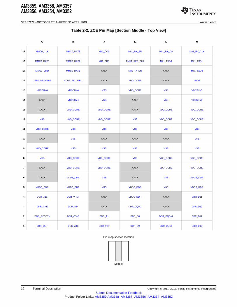
Middle
Pin map section location
AM3359, AM3358, AM3357AM3356, AM3354, AM3352
SPRS717F –OCTOBER 2011–REVISED APRIL 2013 www.ti.com
Table 2-2. ZCE Pin Map [Section Middle - Top View]
G H J K L M
19 MMC0_CLK MMC0_DAT3 MII1_COL MII1_RX_ER MII1_RX_DV MII1_RX_CLK
18 MMC0_DAT0 MMC0_DAT2 MII1_CRS RMII1_REF_CLK MII1_TXD0 MII1_TXD1
17 MMC0_CMD MMC0_DAT1 XXXX MII1_TX_EN XXXX MII1_TXD3
16 USB0_DRVVBUS VDDS_PLL_MPU XXXX VDD_CORE XXXX VDDS
15 VDDSHV4 VDDSHV4 VSS VDD_CORE VSS VDDSHV5
14 XXXX VDDSHV4 VSS XXXX VSS VDDSHV5
13 XXXX VDD_CORE VDD_CORE XXXX VDD_CORE VDD_CORE
12 VSS VDD_CORE VDD_CORE VSS VDD_CORE VDD_CORE
11 VDD_CORE VSS VSS VSS VSS VSS
10 XXXX VSS XXXX XXXX XXXX VSS
9 VDD_CORE VSS VSS VSS VSS VSS
8 VSS VDD_CORE VDD_CORE VSS VDD_CORE VDD_CORE
7 XXXX VDD_CORE VDD_CORE XXXX VDD_CORE VDD_CORE
6 XXXX VDDS_DDR VSS XXXX VSS VDDS_DDR
5 VDDS_DDR VDDS_DDR VSS VDDS_DDR VSS VDDS_DDR
4 DDR_A11 DDR_VREF XXXX VDDS_DDR XXXX DDR_D11
3 DDR_CKE DDR_A14 XXXX DDR_DQM1 XXXX DDR_D10
2 DDR_RESETn DDR_CSn0 DDR_A1 DDR_D8 DDR_DQSn1 DDR_D12
1 DDR_ODT DDR_A13 DDR_VTP DDR_D9 DDR_DQS1 DDR_D13
12 Terminal Description Copyright © 2011–2013, Texas Instruments Incorporated
Submit Documentation FeedbackProduct Folder Links: AM3359 AM3358 AM3357 AM3356 AM3354 AM3352
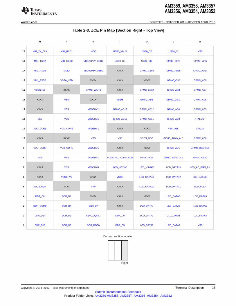
Right
Pin map section location
AM3359, AM3358, AM3357AM3356, AM3354, AM3352
www.ti.com SPRS717F –OCTOBER 2011–REVISED APRIL 2013
Table 2-3. ZCE Pin Map [Section Right - Top View]
N P R T U V W
19 MII1_TX_CLK MII1_RXD1 MDC USB0_VBUS USB0_DP USB0_ID VSS
18 MII1_TXD2 MII1_RXD0 VDDA3P3V_USB0 USB0_CE USB0_DM GPMC_BEn1 GPMC_WPn
17 MII1_RXD3 MDIO VDDA1P8V_USB0 XXXX GPMC_CSn3 GPMC_AD15 GPMC_AD14
16 MII1_RXD2 VSSA_USB XXXX XXXX XXXX GPMC_CLK GPMC_AD9
15 VDDSHV5 XXXX GPMC_WAIT0 XXXX GPMC_CSn2 GPMC_AD8 GPMC_AD7
14 XXXX VSS XXXX VDDS GPMC_AD6 GPMC_CSn1 GPMC_AD5
13 XXXX VSS VDDSHV1 GPMC_AD13 GPMC_AD12 GPMC_AD4 GPMC_AD3
12 VSS VSS VDDSHV1 GPMC_AD10 GPMC_AD11 GPMC_AD2 XTALOUT
11 VDD_CORE VDD_CORE VDDSHV1 XXXX XXXX VSS_OSC XTALIN
10 XXXX XXXX VSS VSS VDDS_OSC GPMC_ADVn_ALE GPMC_AD0
9 VDD_CORE VDD_CORE VDDSHV1 XXXX XXXX GPMC_AD1 GPMC_OEn_REn
8 VSS VSS VDDSHV1 VDDS_PLL_CORE_LCD GPMC_WEn GPMC_BEn0_CLE GPMC_CSn0
7 XXXX VSS VDDSHV6 LCD_HSYNC LCD_VSYNC LCD_DATA15 LCD_AC_BIAS_EN
6 XXXX VDDSHV6 XXXX VDDS LCD_DATA13 LCD_DATA12 LCD_DATA14
5 VDDS_DDR XXXX VPP XXXX LCD_DATA10 LCD_DATA11 LCD_PCLK
4 DDR_D0 DDR_D1 XXXX XXXX XXXX LCD_DATA8 LCD_DATA9
3 DDR_DQM0 DDR_D4 DDR_D7 XXXX LCD_DATA7 LCD_DATA6 LCD_DATA5
2 DDR_D14 DDR_D2 DDR_DQSn0 DDR_D6 LCD_DATA1 LCD_DATA3 LCD_DATA4
1 DDR_D15 DDR_D3 DDR_DQS0 DDR_D5 LCD_DATA0 LCD_DATA2 VSS
Copyright © 2011–2013, Texas Instruments Incorporated Terminal Description 13Submit Documentation Feedback
Product Folder Links: AM3359 AM3358 AM3357 AM3356 AM3354 AM3352
AM3359, AM3358, AM3357AM3356, AM3354, AM3352
SPRS717F –OCTOBER 2011–REVISED APRIL 2013 www.ti.com
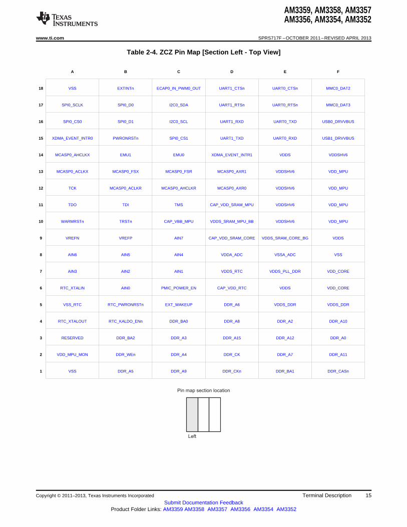
2.1.2 ZCZ Package Pin Maps (Top View)
The pin maps below show the pin assignments on the ZCZ package in three sections (left, middle, andright).
14 Terminal Description Copyright © 2011–2013, Texas Instruments Incorporated
Submit Documentation FeedbackProduct Folder Links: AM3359 AM3358 AM3357 AM3356 AM3354 AM3352
Left
Pin map section location
AM3359, AM3358, AM3357AM3356, AM3354, AM3352
www.ti.com SPRS717F –OCTOBER 2011–REVISED APRIL 2013
Table 2-4. ZCZ Pin Map [Section Left - Top View]
A B C D E F
18 VSS EXTINTn ECAP0_IN_PWM0_OUT UART1_CTSn UART0_CTSn MMC0_DAT2
17 SPI0_SCLK SPI0_D0 I2C0_SDA UART1_RTSn UART0_RTSn MMC0_DAT3
16 SPI0_CS0 SPI0_D1 I2C0_SCL UART1_RXD UART0_TXD USB0_DRVVBUS
15 XDMA_EVENT_INTR0 PWRONRSTn SPI0_CS1 UART1_TXD UART0_RXD USB1_DRVVBUS
14 MCASP0_AHCLKX EMU1 EMU0 XDMA_EVENT_INTR1 VDDS VDDSHV6
13 MCASP0_ACLKX MCASP0_FSX MCASP0_FSR MCASP0_AXR1 VDDSHV6 VDD_MPU
12 TCK MCASP0_ACLKR MCASP0_AHCLKR MCASP0_AXR0 VDDSHV6 VDD_MPU
11 TDO TDI TMS CAP_VDD_SRAM_MPU VDDSHV6 VDD_MPU
10 WARMRSTn TRSTn CAP_VBB_MPU VDDS_SRAM_MPU_BB VDDSHV6 VDD_MPU
9 VREFN VREFP AIN7 CAP_VDD_SRAM_CORE VDDS_SRAM_CORE_BG VDDS
8 AIN6 AIN5 AIN4 VDDA_ADC VSSA_ADC VSS
7 AIN3 AIN2 AIN1 VDDS_RTC VDDS_PLL_DDR VDD_CORE
6 RTC_XTALIN AIN0 PMIC_POWER_EN CAP_VDD_RTC VDDS VDD_CORE
5 VSS_RTC RTC_PWRONRSTn EXT_WAKEUP DDR_A6 VDDS_DDR VDDS_DDR
4 RTC_XTALOUT RTC_KALDO_ENn DDR_BA0 DDR_A8 DDR_A2 DDR_A10
3 RESERVED DDR_BA2 DDR_A3 DDR_A15 DDR_A12 DDR_A0
2 VDD_MPU_MON DDR_WEn DDR_A4 DDR_CK DDR_A7 DDR_A11
1 VSS DDR_A5 DDR_A9 DDR_CKn DDR_BA1 DDR_CASn
Copyright © 2011–2013, Texas Instruments Incorporated Terminal Description 15Submit Documentation Feedback
Product Folder Links: AM3359 AM3358 AM3357 AM3356 AM3354 AM3352
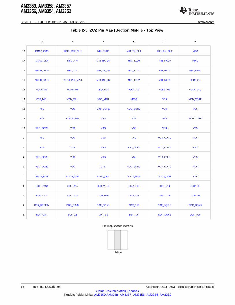
Middle
Pin map section location
AM3359, AM3358, AM3357AM3356, AM3354, AM3352
SPRS717F –OCTOBER 2011–REVISED APRIL 2013 www.ti.com
Table 2-5. ZCZ Pin Map [Section Middle - Top View]
G H J K L M
18 MMC0_CMD RMII1_REF_CLK MII1_TXD3 MII1_TX_CLK MII1_RX_CLK MDC
17 MMC0_CLK MII1_CRS MII1_RX_DV MII1_TXD0 MII1_RXD3 MDIO
16 MMC0_DAT0 MII1_COL MII1_TX_EN MII1_TXD1 MII1_RXD2 MII1_RXD0
15 MMC0_DAT1 VDDS_PLL_MPU MII1_RX_ER MII1_TXD2 MII1_RXD1 USB0_CE
14 VDDSHV6 VDDSHV4 VDDSHV4 VDDSHV5 VDDSHV5 VSSA_USB
13 VDD_MPU VDD_MPU VDD_MPU VDDS VSS VDD_CORE
12 VSS VSS VDD_CORE VDD_CORE VSS VSS
11 VSS VDD_CORE VSS VSS VSS VDD_CORE
10 VDD_CORE VSS VSS VSS VSS VSS
9 VSS VSS VSS VSS VDD_CORE VSS
8 VSS VSS VSS VDD_CORE VDD_CORE VSS
7 VDD_CORE VSS VSS VSS VDD_CORE VSS
6 VDD_CORE VSS VSS VDD_CORE VDD_CORE VSS
5 VDDS_DDR VDDS_DDR VDDS_DDR VDDS_DDR VDDS_DDR VPP
4 DDR_RASn DDR_A14 DDR_VREF DDR_D12 DDR_D14 DDR_D1
3 DDR_CKE DDR_A13 DDR_VTP DDR_D11 DDR_D13 DDR_D0
2 DDR_RESETn DDR_CSn0 DDR_DQM1 DDR_D10 DDR_DQSn1 DDR_DQM0
1 DDR_ODT DDR_A1 DDR_D8 DDR_D9 DDR_DQS1 DDR_D15
16 Terminal Description Copyright © 2011–2013, Texas Instruments Incorporated
Submit Documentation FeedbackProduct Folder Links: AM3359 AM3358 AM3357 AM3356 AM3354 AM3352
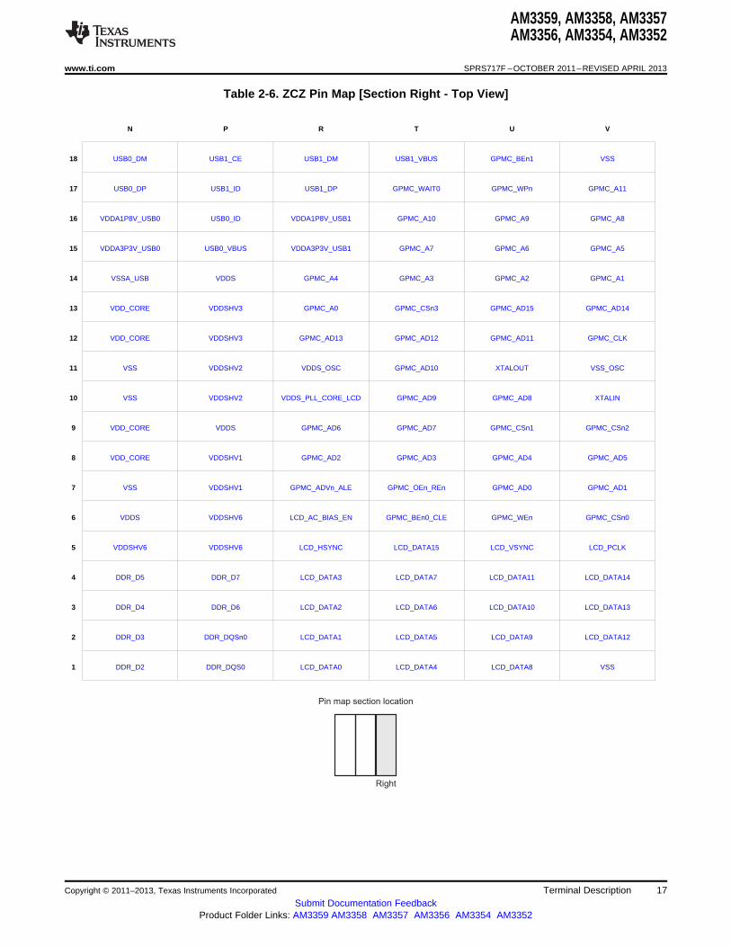
Right
Pin map section location
AM3359, AM3358, AM3357AM3356, AM3354, AM3352
www.ti.com SPRS717F –OCTOBER 2011–REVISED APRIL 2013
Table 2-6. ZCZ Pin Map [Section Right - Top View]
N P R T U V
18 USB0_DM USB1_CE USB1_DM USB1_VBUS GPMC_BEn1 VSS
17 USB0_DP USB1_ID USB1_DP GPMC_WAIT0 GPMC_WPn GPMC_A11
16 VDDA1P8V_USB0 USB0_ID VDDA1P8V_USB1 GPMC_A10 GPMC_A9 GPMC_A8
15 VDDA3P3V_USB0 USB0_VBUS VDDA3P3V_USB1 GPMC_A7 GPMC_A6 GPMC_A5
14 VSSA_USB VDDS GPMC_A4 GPMC_A3 GPMC_A2 GPMC_A1
13 VDD_CORE VDDSHV3 GPMC_A0 GPMC_CSn3 GPMC_AD15 GPMC_AD14
12 VDD_CORE VDDSHV3 GPMC_AD13 GPMC_AD12 GPMC_AD11 GPMC_CLK
11 VSS VDDSHV2 VDDS_OSC GPMC_AD10 XTALOUT VSS_OSC
10 VSS VDDSHV2 VDDS_PLL_CORE_LCD GPMC_AD9 GPMC_AD8 XTALIN
9 VDD_CORE VDDS GPMC_AD6 GPMC_AD7 GPMC_CSn1 GPMC_CSn2
8 VDD_CORE VDDSHV1 GPMC_AD2 GPMC_AD3 GPMC_AD4 GPMC_AD5
7 VSS VDDSHV1 GPMC_ADVn_ALE GPMC_OEn_REn GPMC_AD0 GPMC_AD1
6 VDDS VDDSHV6 LCD_AC_BIAS_EN GPMC_BEn0_CLE GPMC_WEn GPMC_CSn0
5 VDDSHV6 VDDSHV6 LCD_HSYNC LCD_DATA15 LCD_VSYNC LCD_PCLK
4 DDR_D5 DDR_D7 LCD_DATA3 LCD_DATA7 LCD_DATA11 LCD_DATA14
3 DDR_D4 DDR_D6 LCD_DATA2 LCD_DATA6 LCD_DATA10 LCD_DATA13
2 DDR_D3 DDR_DQSn0 LCD_DATA1 LCD_DATA5 LCD_DATA9 LCD_DATA12
1 DDR_D2 DDR_DQS0 LCD_DATA0 LCD_DATA4 LCD_DATA8 VSS
Copyright © 2011–2013, Texas Instruments Incorporated Terminal Description 17Submit Documentation Feedback
Product Folder Links: AM3359 AM3358 AM3357 AM3356 AM3354 AM3352

AM3359, AM3358, AM3357AM3356, AM3354, AM3352
SPRS717F –OCTOBER 2011–REVISED APRIL 2013 www.ti.com
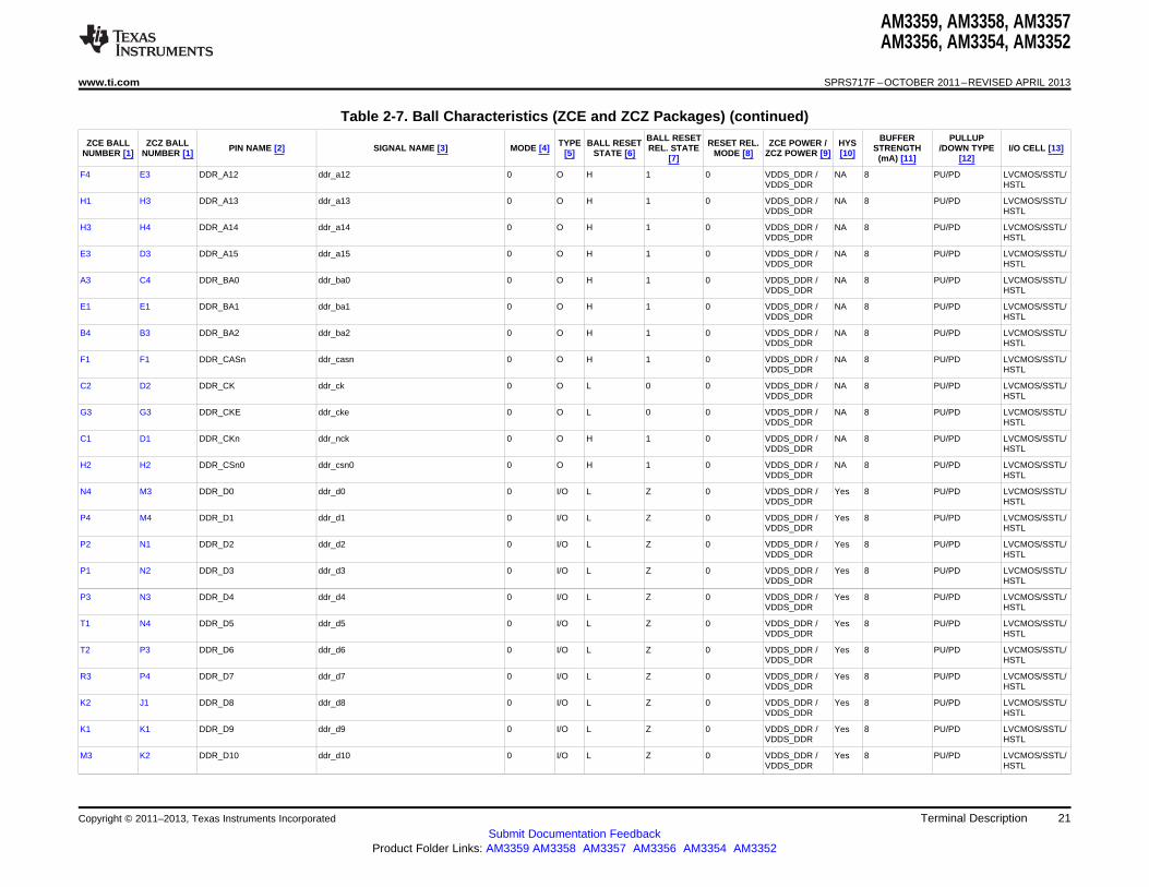
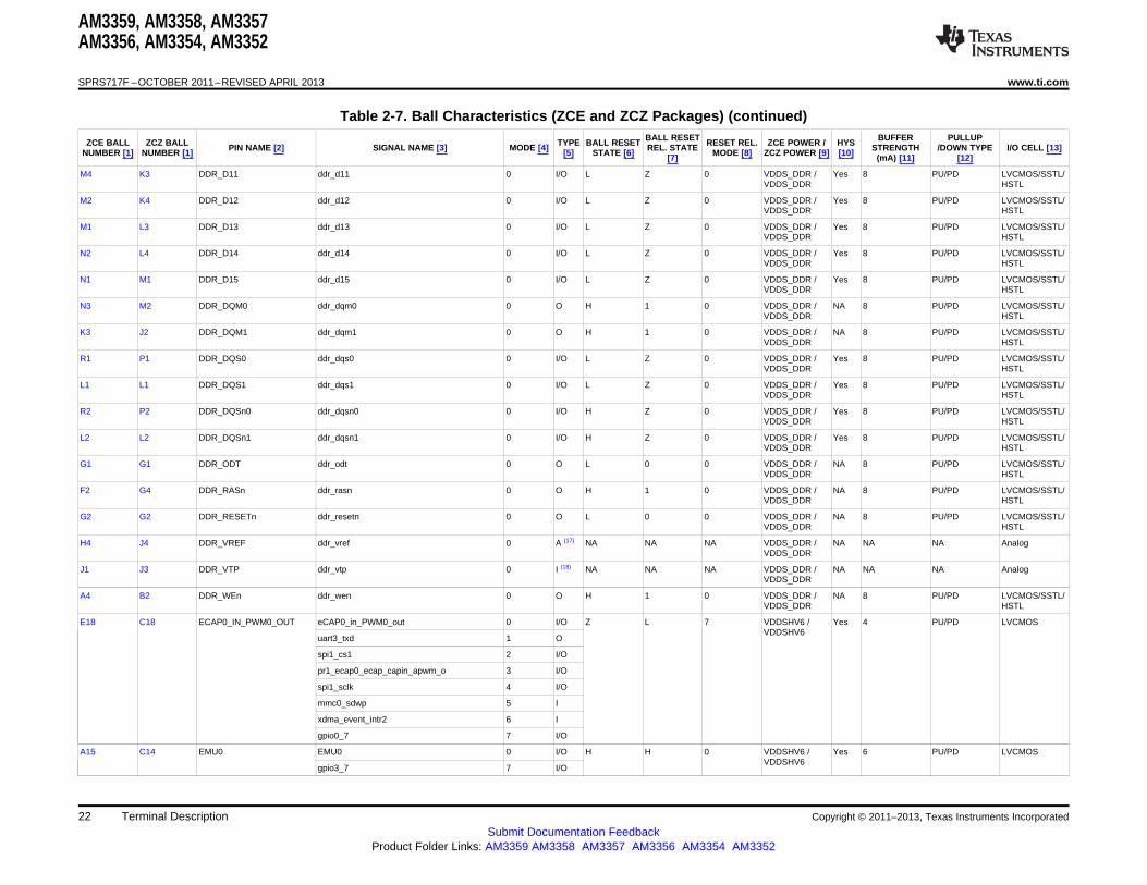
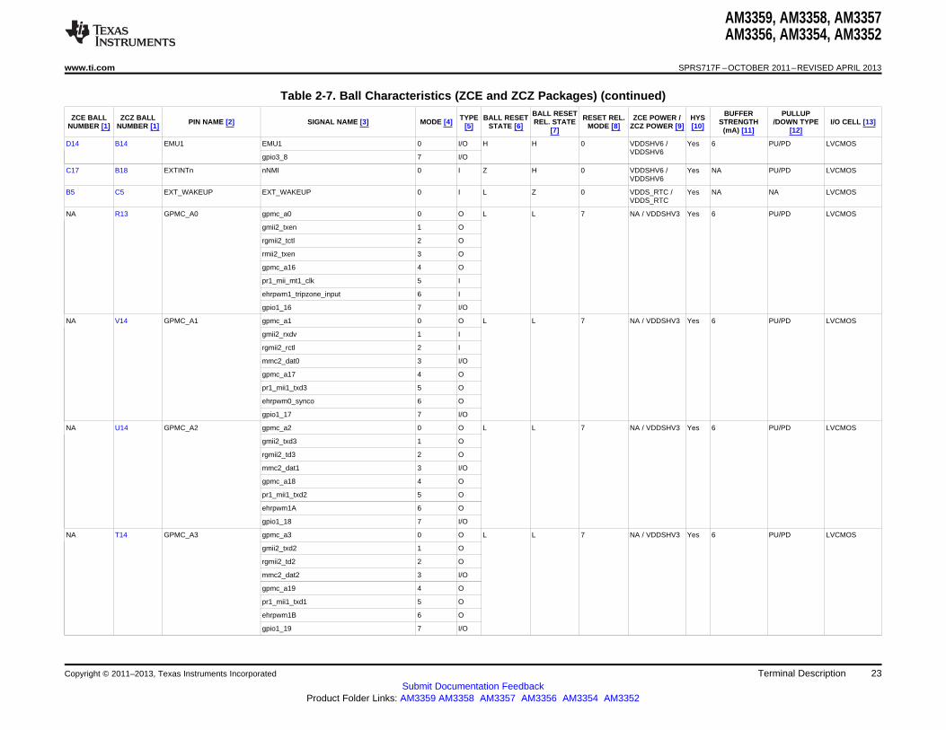
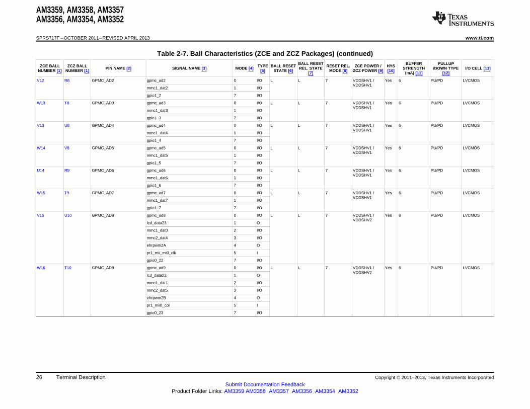
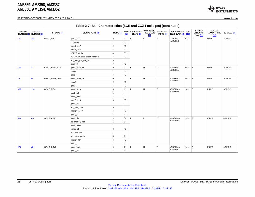
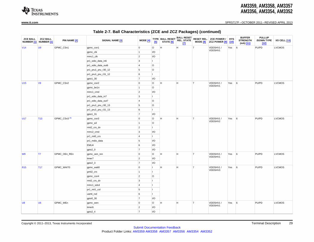
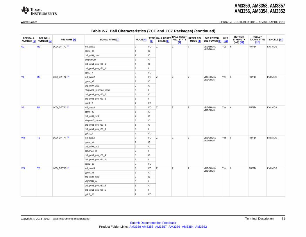
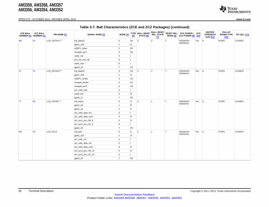
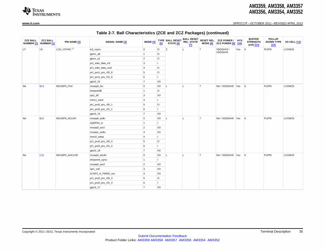
2.2 Ball Characteristics
The AM335x ARM Cortex-A8 Microprocessors (MPUs) Technical Reference Manual (literature numberSPRUH73) and this document may reference internal signal names when discussing peripheral input andoutput signals since many of the AM335x package terminals can be multiplexed to one of severalperipheral signals. The following table has a Pin Name column that lists all device terminal names and aSignal Name column that lists all internal signal names multiplexed to each terminal which provides across reference of internal signal names to terminal names. This table also identifies other importantterminal characteristics.
1. BALL NUMBER: Package ball numbers associated with each signals.
2. PIN NAME: The name of the package pin or terminal.Note: The table does not take into account subsystem terminal multiplexing options.
3. SIGNAL NAME: The signal name for that pin in the mode being used.
4. MODE: Multiplexing mode number.
(a) Mode 0 is the primary mode; this means that when mode 0 is set, the function mapped on theterminal corresponds to the name of the terminal. There is always a function mapped on theprimary mode. Notice that primary mode is not necessarily the default mode.
Note: The default mode is the mode at the release of the reset; also see the RESET REL. MODEcolumn.
(b) Modes 1 to 7 are possible modes for alternate functions. On each terminal, some modes areeffectively used for alternate functions, while some modes are not used and do not correspond to afunctional configuration.
5. TYPE: Signal direction
– I = Input– O = Output– IO = Input and Output– D = Open drain– DS = Differential– A = Analog– PWR = Power– GND = Ground
Note: In the safe_mode, the buffer is configured in high-impedance.
6. BALL RESET STATE: State of the terminal while the active low PWRONRSTn terminal is low.
– 0: The buffer drives VOL (pulldown or pullup resistor not activated)0(PD): The buffer drives VOL with an active pulldown resistor
– 1: The buffer drives VOH (pulldown or pullup resistor not activated)1(PU): The buffer drives VOH with an active pullup resistor
– Z: High-impedance– L: High-impedance with an active pulldown resistor– H : High-impedance with an active pullup resistor
7. BALL RESET REL. STATE: State of the terminal after the active low PWRONRSTn terminaltransitions from low to high.
– 0: The buffer drives VOL (pulldown or pullup resistor not activated)0(PD): The buffer drives VOL with an active pulldown resistor
– 1: The buffer drives VOH (pulldown or pullup resistor not activated)1(PU): The buffer drives VOH with an active pullup resistor
– Z: High-impedance.– L: High-impedance with an active pulldown resistor– H : High-impedance with an active pullup resistor
8. RESET REL. MODE: The mode is automatically configured after the active low PWRONRSTn terminaltransitions from low to high.
18 Terminal Description Copyright © 2011–2013, Texas Instruments Incorporated
Submit Documentation FeedbackProduct Folder Links: AM3359 AM3358 AM3357 AM3356 AM3354 AM3352
AM3359, AM3358, AM3357AM3356, AM3354, AM3352
www.ti.com SPRS717F –OCTOBER 2011–REVISED APRIL 2013
9. POWER: The voltage supply that powers the terminal’s IO buffers.
10. HYS: Indicates if the input buffer is with hysteresis.
11. BUFFER STRENGTH: Drive strength of the associated output buffer.
12. PULLUP OR PULLDOWN TYPE: Denotes the presence of an internal pullup or pulldown resistor.Pullup and pulldown resistors can be enabled or disabled via software.
13. IO CELL: IO cell information.
Note: Configuring two terminals to the same input signal is not supported as it can yield unexpectedresults. This can be easily prevented with the proper software configuration.
Copyright © 2011–2013, Texas Instruments Incorporated Terminal Description 19Submit Documentation Feedback
Product Folder Links: AM3359 AM3358 AM3357 AM3356 AM3354 AM3352

AM3359, AM3358, AM3357AM3356, AM3354, AM3352
SPRS717F –OCTOBER 2011–REVISED APRIL 2013 www.ti.com
Table 2-7. Ball Characteristics (ZCE and ZCZ Packages)
BALL RESET BUFFER PULLUPZCE BALL ZCZ BALL TYPE BALL RESET RESET REL. ZCE POWER / HYSPIN NAME [2] SIGNAL NAME [3] MODE [4] REL. STATE STRENGTH /DOWN TYPE I/O CELL [13]NUMBER [1] NUMBER [1] [5] STATE [6] MODE [8] ZCZ POWER [9] [10][7] (mA) [11] [12]
B8 B6 AIN0 AIN0 0 A (21) Z Z 0 VDDA_ADC / NA 25 NA AnalogVDDA_ADC
A11 C7 AIN1 AIN1 0 A (20) Z Z 0 VDDA_ADC / NA 25 NA AnalogVDDA_ADC
A8 B7 AIN2 AIN2 0 A (20) Z Z 0 VDDA_ADC / NA 25 NA AnalogVDDA_ADC
B11 A7 AIN3 AIN3 0 A (19) Z Z 0 VDDA_ADC / NA 25 NA AnalogVDDA_ADC
C8 C8 AIN4 AIN4 0 A (19) Z Z 0 VDDA_ADC / NA 25 NA AnalogVDDA_ADC
B12 B8 AIN5 AIN5 0 A Z Z 0 VDDA_ADC / NA NA NA AnalogVDDA_ADC
A10 A8 AIN6 AIN6 0 A Z Z 0 VDDA_ADC / NA NA NA AnalogVDDA_ADC
A12 C9 AIN7 AIN7 0 A Z Z 0 VDDA_ADC / NA NA NA AnalogVDDA_ADC
C13 C10 CAP_VBB_MPU CAP_VBB_MPU NA A
D6 D6 CAP_VDD_RTC CAP_VDD_RTC NA A
B10 D9 CAP_VDD_SRAM_CORE CAP_VDD_SRAM_CORE NA A
D13 D11 CAP_VDD_SRAM_MPU CAP_VDD_SRAM_MPU NA A
F3 F3 DDR_A0 ddr_a0 0 O H 1 0 VDDS_DDR / NA 8 PU/PD LVCMOS/SSTL/VDDS_DDR HSTL
J2 H1 DDR_A1 ddr_a1 0 O H 1 0 VDDS_DDR / NA 8 PU/PD LVCMOS/SSTL/VDDS_DDR HSTL
D1 E4 DDR_A2 ddr_a2 0 O H 1 0 VDDS_DDR / NA 8 PU/PD LVCMOS/SSTL/VDDS_DDR HSTL
B3 C3 DDR_A3 ddr_a3 0 O H 1 0 VDDS_DDR / NA 8 PU/PD LVCMOS/SSTL/VDDS_DDR HSTL
E5 C2 DDR_A4 ddr_a4 0 O H 1 0 VDDS_DDR / NA 8 PU/PD LVCMOS/SSTL/VDDS_DDR HSTL
A2 B1 DDR_A5 ddr_a5 0 O H 1 0 VDDS_DDR / NA 8 PU/PD LVCMOS/SSTL/VDDS_DDR HSTL
B1 D5 DDR_A6 ddr_a6 0 O H 1 0 VDDS_DDR / NA 8 PU/PD LVCMOS/SSTL/VDDS_DDR HSTL
D2 E2 DDR_A7 ddr_a7 0 O H 1 0 VDDS_DDR / NA 8 PU/PD LVCMOS/SSTL/VDDS_DDR HSTL
C3 D4 DDR_A8 ddr_a8 0 O H 1 0 VDDS_DDR / NA 8 PU/PD LVCMOS/SSTL/VDDS_DDR HSTL
B2 C1 DDR_A9 ddr_a9 0 O H 1 0 VDDS_DDR / NA 8 PU/PD LVCMOS/SSTL/VDDS_DDR HSTL
E2 F4 DDR_A10 ddr_a10 0 O H 1 0 VDDS_DDR / NA 8 PU/PD LVCMOS/SSTL/VDDS_DDR HSTL
G4 F2 DDR_A11 ddr_a11 0 O H 1 0 VDDS_DDR / NA 8 PU/PD LVCMOS/SSTL/VDDS_DDR HSTL
20 Terminal Description Copyright © 2011–2013, Texas Instruments Incorporated
Submit Documentation FeedbackProduct Folder Links: AM3359 AM3358 AM3357 AM3356 AM3354 AM3352
AM3359, AM3358, AM3357AM3356, AM3354, AM3352
www.ti.com SPRS717F –OCTOBER 2011–REVISED APRIL 2013
Table 2-7. Ball Characteristics (ZCE and ZCZ Packages) (continued)BALL RESET BUFFER PULLUPZCE BALL ZCZ BALL TYPE BALL RESET RESET REL. ZCE POWER / HYSPIN NAME [2] SIGNAL NAME [3] MODE [4] REL. STATE STRENGTH /DOWN TYPE I/O CELL [13]NUMBER [1] NUMBER [1] [5] STATE [6] MODE [8] ZCZ POWER [9] [10][7] (mA) [11] [12]
F4 E3 DDR_A12 ddr_a12 0 O H 1 0 VDDS_DDR / NA 8 PU/PD LVCMOS/SSTL/VDDS_DDR HSTL
H1 H3 DDR_A13 ddr_a13 0 O H 1 0 VDDS_DDR / NA 8 PU/PD LVCMOS/SSTL/VDDS_DDR HSTL
H3 H4 DDR_A14 ddr_a14 0 O H 1 0 VDDS_DDR / NA 8 PU/PD LVCMOS/SSTL/VDDS_DDR HSTL
E3 D3 DDR_A15 ddr_a15 0 O H 1 0 VDDS_DDR / NA 8 PU/PD LVCMOS/SSTL/VDDS_DDR HSTL
A3 C4 DDR_BA0 ddr_ba0 0 O H 1 0 VDDS_DDR / NA 8 PU/PD LVCMOS/SSTL/VDDS_DDR HSTL
E1 E1 DDR_BA1 ddr_ba1 0 O H 1 0 VDDS_DDR / NA 8 PU/PD LVCMOS/SSTL/VDDS_DDR HSTL
B4 B3 DDR_BA2 ddr_ba2 0 O H 1 0 VDDS_DDR / NA 8 PU/PD LVCMOS/SSTL/VDDS_DDR HSTL
F1 F1 DDR_CASn ddr_casn 0 O H 1 0 VDDS_DDR / NA 8 PU/PD LVCMOS/SSTL/VDDS_DDR HSTL
C2 D2 DDR_CK ddr_ck 0 O L 0 0 VDDS_DDR / NA 8 PU/PD LVCMOS/SSTL/VDDS_DDR HSTL
G3 G3 DDR_CKE ddr_cke 0 O L 0 0 VDDS_DDR / NA 8 PU/PD LVCMOS/SSTL/VDDS_DDR HSTL
C1 D1 DDR_CKn ddr_nck 0 O H 1 0 VDDS_DDR / NA 8 PU/PD LVCMOS/SSTL/VDDS_DDR HSTL
H2 H2 DDR_CSn0 ddr_csn0 0 O H 1 0 VDDS_DDR / NA 8 PU/PD LVCMOS/SSTL/VDDS_DDR HSTL
N4 M3 DDR_D0 ddr_d0 0 I/O L Z 0 VDDS_DDR / Yes 8 PU/PD LVCMOS/SSTL/VDDS_DDR HSTL
P4 M4 DDR_D1 ddr_d1 0 I/O L Z 0 VDDS_DDR / Yes 8 PU/PD LVCMOS/SSTL/VDDS_DDR HSTL
P2 N1 DDR_D2 ddr_d2 0 I/O L Z 0 VDDS_DDR / Yes 8 PU/PD LVCMOS/SSTL/VDDS_DDR HSTL
P1 N2 DDR_D3 ddr_d3 0 I/O L Z 0 VDDS_DDR / Yes 8 PU/PD LVCMOS/SSTL/VDDS_DDR HSTL
P3 N3 DDR_D4 ddr_d4 0 I/O L Z 0 VDDS_DDR / Yes 8 PU/PD LVCMOS/SSTL/VDDS_DDR HSTL
T1 N4 DDR_D5 ddr_d5 0 I/O L Z 0 VDDS_DDR / Yes 8 PU/PD LVCMOS/SSTL/VDDS_DDR HSTL
T2 P3 DDR_D6 ddr_d6 0 I/O L Z 0 VDDS_DDR / Yes 8 PU/PD LVCMOS/SSTL/VDDS_DDR HSTL
R3 P4 DDR_D7 ddr_d7 0 I/O L Z 0 VDDS_DDR / Yes 8 PU/PD LVCMOS/SSTL/VDDS_DDR HSTL
K2 J1 DDR_D8 ddr_d8 0 I/O L Z 0 VDDS_DDR / Yes 8 PU/PD LVCMOS/SSTL/VDDS_DDR HSTL
K1 K1 DDR_D9 ddr_d9 0 I/O L Z 0 VDDS_DDR / Yes 8 PU/PD LVCMOS/SSTL/VDDS_DDR HSTL
M3 K2 DDR_D10 ddr_d10 0 I/O L Z 0 VDDS_DDR / Yes 8 PU/PD LVCMOS/SSTL/VDDS_DDR HSTL
Copyright © 2011–2013, Texas Instruments Incorporated Terminal Description 21Submit Documentation Feedback
Product Folder Links: AM3359 AM3358 AM3357 AM3356 AM3354 AM3352
AM3359, AM3358, AM3357AM3356, AM3354, AM3352
SPRS717F –OCTOBER 2011–REVISED APRIL 2013 www.ti.com
Table 2-7. Ball Characteristics (ZCE and ZCZ Packages) (continued)BALL RESET BUFFER PULLUPZCE BALL ZCZ BALL TYPE BALL RESET RESET REL. ZCE POWER / HYSPIN NAME [2] SIGNAL NAME [3] MODE [4] REL. STATE STRENGTH /DOWN TYPE I/O CELL [13]NUMBER [1] NUMBER [1] [5] STATE [6] MODE [8] ZCZ POWER [9] [10][7] (mA) [11] [12]
M4 K3 DDR_D11 ddr_d11 0 I/O L Z 0 VDDS_DDR / Yes 8 PU/PD LVCMOS/SSTL/VDDS_DDR HSTL
M2 K4 DDR_D12 ddr_d12 0 I/O L Z 0 VDDS_DDR / Yes 8 PU/PD LVCMOS/SSTL/VDDS_DDR HSTL
M1 L3 DDR_D13 ddr_d13 0 I/O L Z 0 VDDS_DDR / Yes 8 PU/PD LVCMOS/SSTL/VDDS_DDR HSTL
N2 L4 DDR_D14 ddr_d14 0 I/O L Z 0 VDDS_DDR / Yes 8 PU/PD LVCMOS/SSTL/VDDS_DDR HSTL
N1 M1 DDR_D15 ddr_d15 0 I/O L Z 0 VDDS_DDR / Yes 8 PU/PD LVCMOS/SSTL/VDDS_DDR HSTL
N3 M2 DDR_DQM0 ddr_dqm0 0 O H 1 0 VDDS_DDR / NA 8 PU/PD LVCMOS/SSTL/VDDS_DDR HSTL
K3 J2 DDR_DQM1 ddr_dqm1 0 O H 1 0 VDDS_DDR / NA 8 PU/PD LVCMOS/SSTL/VDDS_DDR HSTL
R1 P1 DDR_DQS0 ddr_dqs0 0 I/O L Z 0 VDDS_DDR / Yes 8 PU/PD LVCMOS/SSTL/VDDS_DDR HSTL
L1 L1 DDR_DQS1 ddr_dqs1 0 I/O L Z 0 VDDS_DDR / Yes 8 PU/PD LVCMOS/SSTL/VDDS_DDR HSTL
R2 P2 DDR_DQSn0 ddr_dqsn0 0 I/O H Z 0 VDDS_DDR / Yes 8 PU/PD LVCMOS/SSTL/VDDS_DDR HSTL
L2 L2 DDR_DQSn1 ddr_dqsn1 0 I/O H Z 0 VDDS_DDR / Yes 8 PU/PD LVCMOS/SSTL/VDDS_DDR HSTL
G1 G1 DDR_ODT ddr_odt 0 O L 0 0 VDDS_DDR / NA 8 PU/PD LVCMOS/SSTL/VDDS_DDR HSTL
F2 G4 DDR_RASn ddr_rasn 0 O H 1 0 VDDS_DDR / NA 8 PU/PD LVCMOS/SSTL/VDDS_DDR HSTL
G2 G2 DDR_RESETn ddr_resetn 0 O L 0 0 VDDS_DDR / NA 8 PU/PD LVCMOS/SSTL/VDDS_DDR HSTL
H4 J4 DDR_VREF ddr_vref 0 A (17) NA NA NA VDDS_DDR / NA NA NA AnalogVDDS_DDR
J1 J3 DDR_VTP ddr_vtp 0 I (18) NA NA NA VDDS_DDR / NA NA NA AnalogVDDS_DDR
A4 B2 DDR_WEn ddr_wen 0 O H 1 0 VDDS_DDR / NA 8 PU/PD LVCMOS/SSTL/VDDS_DDR HSTL
E18 C18 ECAP0_IN_PWM0_OUT eCAP0_in_PWM0_out 0 I/O Z L 7 VDDSHV6 / Yes 4 PU/PD LVCMOSVDDSHV6
uart3_txd 1 O
spi1_cs1 2 I/O
pr1_ecap0_ecap_capin_apwm_o 3 I/O
spi1_sclk 4 I/O
mmc0_sdwp 5 I
xdma_event_intr2 6 I
gpio0_7 7 I/O
A15 C14 EMU0 EMU0 0 I/O H H 0 VDDSHV6 / Yes 6 PU/PD LVCMOSVDDSHV6
gpio3_7 7 I/O
22 Terminal Description Copyright © 2011–2013, Texas Instruments Incorporated
Submit Documentation FeedbackProduct Folder Links: AM3359 AM3358 AM3357 AM3356 AM3354 AM3352
AM3359, AM3358, AM3357AM3356, AM3354, AM3352
www.ti.com SPRS717F –OCTOBER 2011–REVISED APRIL 2013
Table 2-7. Ball Characteristics (ZCE and ZCZ Packages) (continued)BALL RESET BUFFER PULLUPZCE BALL ZCZ BALL TYPE BALL RESET RESET REL. ZCE POWER / HYSPIN NAME [2] SIGNAL NAME [3] MODE [4] REL. STATE STRENGTH /DOWN TYPE I/O CELL [13]NUMBER [1] NUMBER [1] [5] STATE [6] MODE [8] ZCZ POWER [9] [10][7] (mA) [11] [12]
D14 B14 EMU1 EMU1 0 I/O H H 0 VDDSHV6 / Yes 6 PU/PD LVCMOSVDDSHV6
gpio3_8 7 I/O
C17 B18 EXTINTn nNMI 0 I Z H 0 VDDSHV6 / Yes NA PU/PD LVCMOSVDDSHV6
B5 C5 EXT_WAKEUP EXT_WAKEUP 0 I L Z 0 VDDS_RTC / Yes NA NA LVCMOSVDDS_RTC
NA R13 GPMC_A0 gpmc_a0 0 O L L 7 NA / VDDSHV3 Yes 6 PU/PD LVCMOS
gmii2_txen 1 O
rgmii2_tctl 2 O
rmii2_txen 3 O
gpmc_a16 4 O
pr1_mii_mt1_clk 5 I
ehrpwm1_tripzone_input 6 I
gpio1_16 7 I/O
NA V14 GPMC_A1 gpmc_a1 0 O L L 7 NA / VDDSHV3 Yes 6 PU/PD LVCMOS
gmii2_rxdv 1 I
rgmii2_rctl 2 I
mmc2_dat0 3 I/O
gpmc_a17 4 O
pr1_mii1_txd3 5 O
ehrpwm0_synco 6 O
gpio1_17 7 I/O
NA U14 GPMC_A2 gpmc_a2 0 O L L 7 NA / VDDSHV3 Yes 6 PU/PD LVCMOS
gmii2_txd3 1 O
rgmii2_td3 2 O
mmc2_dat1 3 I/O
gpmc_a18 4 O
pr1_mii1_txd2 5 O
ehrpwm1A 6 O
gpio1_18 7 I/O
NA T14 GPMC_A3 gpmc_a3 0 O L L 7 NA / VDDSHV3 Yes 6 PU/PD LVCMOS
gmii2_txd2 1 O
rgmii2_td2 2 O
mmc2_dat2 3 I/O
gpmc_a19 4 O
pr1_mii1_txd1 5 O
ehrpwm1B 6 O
gpio1_19 7 I/O
Copyright © 2011–2013, Texas Instruments Incorporated Terminal Description 23Submit Documentation Feedback
Product Folder Links: AM3359 AM3358 AM3357 AM3356 AM3354 AM3352

AM3359, AM3358, AM3357AM3356, AM3354, AM3352
SPRS717F –OCTOBER 2011–REVISED APRIL 2013 www.ti.com
Table 2-7. Ball Characteristics (ZCE and ZCZ Packages) (continued)BALL RESET BUFFER PULLUPZCE BALL ZCZ BALL TYPE BALL RESET RESET REL. ZCE POWER / HYSPIN NAME [2] SIGNAL NAME [3] MODE [4] REL. STATE STRENGTH /DOWN TYPE I/O CELL [13]NUMBER [1] NUMBER [1] [5] STATE [6] MODE [8] ZCZ POWER [9] [10][7] (mA) [11] [12]
NA R14 GPMC_A4 gpmc_a4 0 O L L 7 NA / VDDSHV3 Yes 6 PU/PD LVCMOS
gmii2_txd1 1 O
rgmii2_td1 2 O
rmii2_txd1 3 O
gpmc_a20 4 O
pr1_mii1_txd0 5 O
eQEP1A_in 6 I
gpio1_20 7 I/O
NA V15 GPMC_A5 gpmc_a5 0 O L L 7 NA / VDDSHV3 Yes 6 PU/PD LVCMOS
gmii2_txd0 1 O
rgmii2_td0 2 O
rmii2_txd0 3 O
gpmc_a21 4 O
pr1_mii1_rxd3 5 I
eQEP1B_in 6 I
gpio1_21 7 I/O
NA U15 GPMC_A6 gpmc_a6 0 O L L 7 NA / VDDSHV3 Yes 6 PU/PD LVCMOS
gmii2_txclk 1 I
rgmii2_tclk 2 O
mmc2_dat4 3 I/O
gpmc_a22 4 O
pr1_mii1_rxd2 5 I
eQEP1_index 6 I/O
gpio1_22 7 I/O
NA T15 GPMC_A7 gpmc_a7 0 O L L 7 NA / VDDSHV3 Yes 6 PU/PD LVCMOS
gmii2_rxclk 1 I
rgmii2_rclk 2 I
mmc2_dat5 3 I/O
gpmc_a23 4 O
pr1_mii1_rxd1 5 I
eQEP1_strobe 6 I/O
gpio1_23 7 I/O
24 Terminal Description Copyright © 2011–2013, Texas Instruments Incorporated
Submit Documentation FeedbackProduct Folder Links: AM3359 AM3358 AM3357 AM3356 AM3354 AM3352

AM3359, AM3358, AM3357AM3356, AM3354, AM3352
www.ti.com SPRS717F –OCTOBER 2011–REVISED APRIL 2013
Table 2-7. Ball Characteristics (ZCE and ZCZ Packages) (continued)BALL RESET BUFFER PULLUPZCE BALL ZCZ BALL TYPE BALL RESET RESET REL. ZCE POWER / HYSPIN NAME [2] SIGNAL NAME [3] MODE [4] REL. STATE STRENGTH /DOWN TYPE I/O CELL [13]NUMBER [1] NUMBER [1] [5] STATE [6] MODE [8] ZCZ POWER [9] [10][7] (mA) [11] [12]
NA V16 GPMC_A8 gpmc_a8 0 O L L 7 NA / VDDSHV3 Yes 6 PU/PD LVCMOS
gmii2_rxd3 1 I
rgmii2_rd3 2 I
mmc2_dat6 3 I/O
gpmc_a24 4 O
pr1_mii1_rxd0 5 I
mcasp0_aclkx 6 I/O
gpio1_24 7 I/O
NA U16 GPMC_A9 (10) gpmc_a9 0 O L L 7 NA / VDDSHV3 Yes 6 PU/PD LVCMOS
gmii2_rxd2 1 I
rgmii2_rd2 2 I
mmc2_dat7 / rmii2_crs_dv 3 I/O
gpmc_a25 4 O
pr1_mii_mr1_clk 5 I
mcasp0_fsx 6 I/O
gpio1_25 7 I/O
NA T16 GPMC_A10 gpmc_a10 0 O L L 7 NA / VDDSHV3 Yes 6 PU/PD LVCMOS
gmii2_rxd1 1 I
rgmii2_rd1 2 I
rmii2_rxd1 3 I
gpmc_a26 4 O
pr1_mii1_rxdv 5 I
mcasp0_axr0 6 I/O
gpio1_26 7 I/O
NA V17 GPMC_A11 gpmc_a11 0 O L L 7 NA / VDDSHV3 Yes 6 PU/PD LVCMOS
gmii2_rxd0 1 I
rgmii2_rd0 2 I
rmii2_rxd0 3 I
gpmc_a27 4 O
pr1_mii1_rxer 5 I
mcasp0_axr1 6 I/O
gpio1_27 7 I/O
W10 U7 GPMC_AD0 gpmc_ad0 0 I/O L L 7 VDDSHV1 / Yes 6 PU/PD LVCMOSVDDSHV1
mmc1_dat0 1 I/O
gpio1_0 7 I/O
V9 V7 GPMC_AD1 gpmc_ad1 0 I/O L L 7 VDDSHV1 / Yes 6 PU/PD LVCMOSVDDSHV1
mmc1_dat1 1 I/O
gpio1_1 7 I/O
Copyright © 2011–2013, Texas Instruments Incorporated Terminal Description 25Submit Documentation Feedback
Product Folder Links: AM3359 AM3358 AM3357 AM3356 AM3354 AM3352
AM3359, AM3358, AM3357AM3356, AM3354, AM3352
SPRS717F –OCTOBER 2011–REVISED APRIL 2013 www.ti.com
Table 2-7. Ball Characteristics (ZCE and ZCZ Packages) (continued)BALL RESET BUFFER PULLUPZCE BALL ZCZ BALL TYPE BALL RESET RESET REL. ZCE POWER / HYSPIN NAME [2] SIGNAL NAME [3] MODE [4] REL. STATE STRENGTH /DOWN TYPE I/O CELL [13]NUMBER [1] NUMBER [1] [5] STATE [6] MODE [8] ZCZ POWER [9] [10][7] (mA) [11] [12]
V12 R8 GPMC_AD2 gpmc_ad2 0 I/O L L 7 VDDSHV1 / Yes 6 PU/PD LVCMOSVDDSHV1
mmc1_dat2 1 I/O
gpio1_2 7 I/O
W13 T8 GPMC_AD3 gpmc_ad3 0 I/O L L 7 VDDSHV1 / Yes 6 PU/PD LVCMOSVDDSHV1
mmc1_dat3 1 I/O
gpio1_3 7 I/O
V13 U8 GPMC_AD4 gpmc_ad4 0 I/O L L 7 VDDSHV1 / Yes 6 PU/PD LVCMOSVDDSHV1
mmc1_dat4 1 I/O
gpio1_4 7 I/O
W14 V8 GPMC_AD5 gpmc_ad5 0 I/O L L 7 VDDSHV1 / Yes 6 PU/PD LVCMOSVDDSHV1
mmc1_dat5 1 I/O
gpio1_5 7 I/O
U14 R9 GPMC_AD6 gpmc_ad6 0 I/O L L 7 VDDSHV1 / Yes 6 PU/PD LVCMOSVDDSHV1
mmc1_dat6 1 I/O
gpio1_6 7 I/O
W15 T9 GPMC_AD7 gpmc_ad7 0 I/O L L 7 VDDSHV1 / Yes 6 PU/PD LVCMOSVDDSHV1
mmc1_dat7 1 I/O
gpio1_7 7 I/O
V15 U10 GPMC_AD8 gpmc_ad8 0 I/O L L 7 VDDSHV1 / Yes 6 PU/PD LVCMOSVDDSHV2
lcd_data23 1 O
mmc1_dat0 2 I/O
mmc2_dat4 3 I/O
ehrpwm2A 4 O
pr1_mii_mt0_clk 5 I
gpio0_22 7 I/O
W16 T10 GPMC_AD9 gpmc_ad9 0 I/O L L 7 VDDSHV1 / Yes 6 PU/PD LVCMOSVDDSHV2
lcd_data22 1 O
mmc1_dat1 2 I/O
mmc2_dat5 3 I/O
ehrpwm2B 4 O
pr1_mii0_col 5 I
gpio0_23 7 I/O
26 Terminal Description Copyright © 2011–2013, Texas Instruments Incorporated
Submit Documentation FeedbackProduct Folder Links: AM3359 AM3358 AM3357 AM3356 AM3354 AM3352

AM3359, AM3358, AM3357AM3356, AM3354, AM3352
www.ti.com SPRS717F –OCTOBER 2011–REVISED APRIL 2013
Table 2-7. Ball Characteristics (ZCE and ZCZ Packages) (continued)BALL RESET BUFFER PULLUPZCE BALL ZCZ BALL TYPE BALL RESET RESET REL. ZCE POWER / HYSPIN NAME [2] SIGNAL NAME [3] MODE [4] REL. STATE STRENGTH /DOWN TYPE I/O CELL [13]NUMBER [1] NUMBER [1] [5] STATE [6] MODE [8] ZCZ POWER [9] [10][7] (mA) [11] [12]
T12 T11 GPMC_AD10 gpmc_ad10 0 I/O L L 7 VDDSHV1 / Yes 6 PU/PD LVCMOSVDDSHV2
lcd_data21 1 O
mmc1_dat2 2 I/O
mmc2_dat6 3 I/O
ehrpwm2_tripzone_input 4 I
pr1_mii0_txen 5 O
gpio0_26 7 I/O
U12 U12 GPMC_AD11 gpmc_ad11 0 I/O L L 7 VDDSHV1 / Yes 6 PU/PD LVCMOSVDDSHV2
lcd_data20 1 O
mmc1_dat3 2 I/O
mmc2_dat7 3 I/O
ehrpwm0_synco 4 O
pr1_mii0_txd3 5 O
gpio0_27 7 I/O
U13 T12 GPMC_AD12 gpmc_ad12 0 I/O L L 7 VDDSHV1 / Yes 6 PU/PD LVCMOSVDDSHV2
lcd_data19 1 O
mmc1_dat4 2 I/O
mmc2_dat0 3 I/O
eQEP2A_in 4 I
pr1_mii0_txd2 5 O
pr1_pru0_pru_r30_14 6 O
gpio1_12 7 I/O
T13 R12 GPMC_AD13 gpmc_ad13 0 I/O L L 7 VDDSHV1 / Yes 6 PU/PD LVCMOSVDDSHV2
lcd_data18 1 O
mmc1_dat5 2 I/O
mmc2_dat1 3 I/O
eQEP2B_in 4 I
pr1_mii0_txd1 5 O
pr1_pru0_pru_r30_15 6 O
gpio1_13 7 I/O
W17 V13 GPMC_AD14 gpmc_ad14 0 I/O L L 7 VDDSHV1 / Yes 6 PU/PD LVCMOSVDDSHV2
lcd_data17 1 O
mmc1_dat6 2 I/O
mmc2_dat2 3 I/O
eQEP2_index 4 I/O
pr1_mii0_txd0 5 O
pr1_pru0_pru_r31_14 6 I
gpio1_14 7 I/O
Copyright © 2011–2013, Texas Instruments Incorporated Terminal Description 27Submit Documentation Feedback
Product Folder Links: AM3359 AM3358 AM3357 AM3356 AM3354 AM3352
AM3359, AM3358, AM3357AM3356, AM3354, AM3352
SPRS717F –OCTOBER 2011–REVISED APRIL 2013 www.ti.com
Table 2-7. Ball Characteristics (ZCE and ZCZ Packages) (continued)BALL RESET BUFFER PULLUPZCE BALL ZCZ BALL TYPE BALL RESET RESET REL. ZCE POWER / HYSPIN NAME [2] SIGNAL NAME [3] MODE [4] REL. STATE STRENGTH /DOWN TYPE I/O CELL [13]NUMBER [1] NUMBER [1] [5] STATE [6] MODE [8] ZCZ POWER [9] [10][7] (mA) [11] [12]
V17 U13 GPMC_AD15 gpmc_ad15 0 I/O L L 7 VDDSHV1 / Yes 6 PU/PD LVCMOSVDDSHV2
lcd_data16 1 O
mmc1_dat7 2 I/O
mmc2_dat3 3 I/O
eQEP2_strobe 4 I/O
pr1_ecap0_ecap_capin_apwm_o 5 I/O
pr1_pru0_pru_r31_15 6 I
gpio1_15 7 I/O
V10 R7 GPMC_ADVn_ALE gpmc_advn_ale 0 O H H 7 VDDSHV1 / Yes 6 PU/PD LVCMOSVDDSHV1
timer4 2 I/O
gpio2_2 7 I/O
V8 T6 GPMC_BEn0_CLE gpmc_be0n_cle 0 O H H 7 VDDSHV1 / Yes 6 PU/PD LVCMOSVDDSHV1
timer5 2 I/O
gpio2_5 7 I/O
V18 U18 GPMC_BEn1 gpmc_be1n 0 O H H 7 VDDSHV1 / Yes 6 PU/PD LVCMOSVDDSHV3
gmii2_col 1 I
gpmc_csn6 2 O
mmc2_dat3 3 I/O
gpmc_dir 4 O
pr1_mii1_rxlink 5 I
mcasp0_aclkr 6 I/O
gpio1_28 7 I/O
V16 V12 GPMC_CLK gpmc_clk 0 I/O L L 7 VDDSHV1 / Yes 6 PU/PD LVCMOSVDDSHV2
lcd_memory_clk 1 O
gpmc_wait1 2 I
mmc2_clk 3 I/O
pr1_mii1_crs 4 I
pr1_mdio_mdclk 5 O
mcasp0_fsr 6 I/O
gpio2_1 7 I/O
W8 V6 GPMC_CSn0 gpmc_csn0 0 O H H 7 VDDSHV1 / Yes 6 PU/PD LVCMOSVDDSHV1
gpio1_29 7 I/O
28 Terminal Description Copyright © 2011–2013, Texas Instruments Incorporated
Submit Documentation FeedbackProduct Folder Links: AM3359 AM3358 AM3357 AM3356 AM3354 AM3352
AM3359, AM3358, AM3357AM3356, AM3354, AM3352
www.ti.com SPRS717F –OCTOBER 2011–REVISED APRIL 2013
Table 2-7. Ball Characteristics (ZCE and ZCZ Packages) (continued)BALL RESET BUFFER PULLUPZCE BALL ZCZ BALL TYPE BALL RESET RESET REL. ZCE POWER / HYSPIN NAME [2] SIGNAL NAME [3] MODE [4] REL. STATE STRENGTH /DOWN TYPE I/O CELL [13]NUMBER [1] NUMBER [1] [5] STATE [6] MODE [8] ZCZ POWER [9] [10][7] (mA) [11] [12]
V14 U9 GPMC_CSn1 gpmc_csn1 0 O H H 7 VDDSHV1 / Yes 6 PU/PD LVCMOSVDDSHV1
gpmc_clk 1 I/O
mmc1_clk 2 I/O
pr1_edio_data_in6 3 I
pr1_edio_data_out6 4 O
pr1_pru1_pru_r30_12 5 O
pr1_pru1_pru_r31_12 6 I
gpio1_30 7 I/O
U15 V9 GPMC_CSn2 gpmc_csn2 0 O H H 7 VDDSHV1 / Yes 6 PU/PD LVCMOSVDDSHV1
gpmc_be1n 1 O
mmc1_cmd 2 I/O
pr1_edio_data_in7 3 I
pr1_edio_data_out7 4 O
pr1_pru1_pru_r30_13 5 O
pr1_pru1_pru_r31_13 6 I
gpio1_31 7 I/O
U17 T13 GPMC_CSn3 (6) gpmc_csn3 0 O H H 7 VDDSHV1 / Yes 6 PU/PD LVCMOSVDDSHV2
gpmc_a3 1 O
rmii2_crs_dv 2 I
mmc2_cmd 3 I/O
pr1_mii0_crs 4 I
pr1_mdio_data 5 I/O
EMU4 6 I/O
gpio2_0 7 I/O
W9 T7 GPMC_OEn_REn gpmc_oen_ren 0 O H H 7 VDDSHV1 / Yes 6 PU/PD LVCMOSVDDSHV1
timer7 2 I/O
gpio2_3 7 I/O
R15 T17 GPMC_WAIT0 gpmc_wait0 0 I H H 7 VDDSHV1 / Yes 6 PU/PD LVCMOSVDDSHV3
gmii2_crs 1 I
gpmc_csn4 2 O
rmii2_crs_dv 3 I
mmc1_sdcd 4 I
pr1_mii1_col 5 I
uart4_rxd 6 I
gpio0_30 7 I/O
U8 U6 GPMC_WEn gpmc_wen 0 O H H 7 VDDSHV1 / Yes 6 PU/PD LVCMOSVDDSHV1
timer6 2 I/O
gpio2_4 7 I/O
Copyright © 2011–2013, Texas Instruments Incorporated Terminal Description 29Submit Documentation Feedback
Product Folder Links: AM3359 AM3358 AM3357 AM3356 AM3354 AM3352

AM3359, AM3358, AM3357AM3356, AM3354, AM3352
SPRS717F –OCTOBER 2011–REVISED APRIL 2013 www.ti.com
Table 2-7. Ball Characteristics (ZCE and ZCZ Packages) (continued)BALL RESET BUFFER PULLUPZCE BALL ZCZ BALL TYPE BALL RESET RESET REL. ZCE POWER / HYSPIN NAME [2] SIGNAL NAME [3] MODE [4] REL. STATE STRENGTH /DOWN TYPE I/O CELL [13]NUMBER [1] NUMBER [1] [5] STATE [6] MODE [8] ZCZ POWER [9] [10][7] (mA) [11] [12]
W18 U17 GPMC_WPn gpmc_wpn 0 O H H 7 VDDSHV1 / Yes 6 PU/PD LVCMOSVDDSHV3
gmii2_rxerr 1 I
gpmc_csn5 2 O
rmii2_rxerr 3 I
mmc2_sdcd 4 I
pr1_mii1_txen 5 O
uart4_txd 6 O
gpio0_31 7 I/O
C18 C17 I2C0_SDA I2C0_SDA 0 I/OD Z H 7 VDDSHV6 / Yes 4 PU/PD LVCMOSVDDSHV6
timer4 1 I/O
uart2_ctsn 2 I
eCAP2_in_PWM2_out 3 I/O
gpio3_5 7 I/O
B19 C16 I2C0_SCL I2C0_SCL 0 I/OD Z H 7 VDDSHV6 / Yes 4 PU/PD LVCMOSVDDSHV6
timer7 1 I/O
uart2_rtsn 2 O
eCAP1_in_PWM1_out 3 I/O
gpio3_6 7 I/O
W7 R6 LCD_AC_BIAS_EN lcd_ac_bias_en 0 O Z L 7 VDDSHV6 / Yes 6 PU/PD LVCMOSVDDSHV6
gpmc_a11 1 O
pr1_mii1_crs 2 I
pr1_edio_data_in5 3 I
pr1_edio_data_out5 4 O
pr1_pru1_pru_r30_11 5 O
pr1_pru1_pru_r31_11 6 I
gpio2_25 7 I/O
U1 R1 LCD_DATA0 (5) lcd_data0 0 I/O Z Z 7 VDDSHV6 / Yes 6 PU/PD LVCMOSVDDSHV6
gpmc_a0 1 O
pr1_mii_mt0_clk 2 I
ehrpwm2A 3 O
pr1_pru1_pru_r30_0 5 O
pr1_pru1_pru_r31_0 6 I
gpio2_6 7 I/O
30 Terminal Description Copyright © 2011–2013, Texas Instruments Incorporated
Submit Documentation FeedbackProduct Folder Links: AM3359 AM3358 AM3357 AM3356 AM3354 AM3352
AM3359, AM3358, AM3357AM3356, AM3354, AM3352
www.ti.com SPRS717F –OCTOBER 2011–REVISED APRIL 2013
Table 2-7. Ball Characteristics (ZCE and ZCZ Packages) (continued)BALL RESET BUFFER PULLUPZCE BALL ZCZ BALL TYPE BALL RESET RESET REL. ZCE POWER / HYSPIN NAME [2] SIGNAL NAME [3] MODE [4] REL. STATE STRENGTH /DOWN TYPE I/O CELL [13]NUMBER [1] NUMBER [1] [5] STATE [6] MODE [8] ZCZ POWER [9] [10][7] (mA) [11] [12]
U2 R2 LCD_DATA1 (5) lcd_data1 0 I/O Z Z 7 VDDSHV6 / Yes 6 PU/PD LVCMOSVDDSHV6
gpmc_a1 1 O
pr1_mii0_txen 2 O
ehrpwm2B 3 O
pr1_pru1_pru_r30_1 5 O
pr1_pru1_pru_r31_1 6 I
gpio2_7 7 I/O
V1 R3 LCD_DATA2 (5) lcd_data2 0 I/O Z Z 7 VDDSHV6 / Yes 6 PU/PD LVCMOSVDDSHV6
gpmc_a2 1 O
pr1_mii0_txd3 2 O
ehrpwm2_tripzone_input 3 I
pr1_pru1_pru_r30_2 5 O
pr1_pru1_pru_r31_2 6 I
gpio2_8 7 I/O
V2 R4 LCD_DATA3 (5) lcd_data3 0 I/O Z Z 7 VDDSHV6 / Yes 6 PU/PD LVCMOSVDDSHV6
gpmc_a3 1 O
pr1_mii0_txd2 2 O
ehrpwm0_synco 3 O
pr1_pru1_pru_r30_3 5 O
pr1_pru1_pru_r31_3 6 I
gpio2_9 7 I/O
W2 T1 LCD_DATA4 (5) lcd_data4 0 I/O Z Z 7 VDDSHV6 / Yes 6 PU/PD LVCMOSVDDSHV6
gpmc_a4 1 O
pr1_mii0_txd1 2 O
eQEP2A_in 3 I
pr1_pru1_pru_r30_4 5 O
pr1_pru1_pru_r31_4 6 I
gpio2_10 7 I/O
W3 T2 LCD_DATA5 (5) lcd_data5 0 I/O Z Z 7 VDDSHV6 / Yes 6 PU/PD LVCMOSVDDSHV6
gpmc_a5 1 O
pr1_mii0_txd0 2 O
eQEP2B_in 3 I
pr1_pru1_pru_r30_5 5 O
pr1_pru1_pru_r31_5 6 I
gpio2_11 7 I/O
Copyright © 2011–2013, Texas Instruments Incorporated Terminal Description 31Submit Documentation Feedback
Product Folder Links: AM3359 AM3358 AM3357 AM3356 AM3354 AM3352

AM3359, AM3358, AM3357AM3356, AM3354, AM3352
SPRS717F –OCTOBER 2011–REVISED APRIL 2013 www.ti.com
Table 2-7. Ball Characteristics (ZCE and ZCZ Packages) (continued)BALL RESET BUFFER PULLUPZCE BALL ZCZ BALL TYPE BALL RESET RESET REL. ZCE POWER / HYSPIN NAME [2] SIGNAL NAME [3] MODE [4] REL. STATE STRENGTH /DOWN TYPE I/O CELL [13]NUMBER [1] NUMBER [1] [5] STATE [6] MODE [8] ZCZ POWER [9] [10][7] (mA) [11] [12]
V3 T3 LCD_DATA6 (5) lcd_data6 0 I/O Z Z 7 VDDSHV6 / Yes 6 PU/PD LVCMOSVDDSHV6
gpmc_a6 1 O
pr1_edio_data_in6 2 I
eQEP2_index 3 I/O
pr1_edio_data_out6 4 O
pr1_pru1_pru_r30_6 5 O
pr1_pru1_pru_r31_6 6 I
gpio2_12 7 I/O
U3 T4 LCD_DATA7 (5) lcd_data7 0 I/O Z Z 7 VDDSHV6 / Yes 6 PU/PD LVCMOSVDDSHV6
gpmc_a7 1 O
pr1_edio_data_in7 2 I
eQEP2_strobe 3 I/O
pr1_edio_data_out7 4 O
pr1_pru1_pru_r30_7 5 O
pr1_pru1_pru_r31_7 6 I
gpio2_13 7 I/O
V4 U1 LCD_DATA8 (5) lcd_data8 0 I/O Z Z 7 VDDSHV6 / Yes 6 PU/PD LVCMOSVDDSHV6
gpmc_a12 1 O
ehrpwm1_tripzone_input 2 I
mcasp0_aclkx 3 I/O
uart5_txd 4 O
pr1_mii0_rxd3 5 I
uart2_ctsn 6 I
gpio2_14 7 I/O
W4 U2 LCD_DATA9 (5) lcd_data9 0 I/O Z Z 7 VDDSHV6 / Yes 6 PU/PD LVCMOSVDDSHV6
gpmc_a13 1 O
ehrpwm0_synco 2 O
mcasp0_fsx 3 I/O
uart5_rxd 4 I
pr1_mii0_rxd2 5 I
uart2_rtsn 6 O
gpio2_15 7 I/O
32 Terminal Description Copyright © 2011–2013, Texas Instruments Incorporated
Submit Documentation FeedbackProduct Folder Links: AM3359 AM3358 AM3357 AM3356 AM3354 AM3352

AM3359, AM3358, AM3357AM3356, AM3354, AM3352
www.ti.com SPRS717F –OCTOBER 2011–REVISED APRIL 2013
Table 2-7. Ball Characteristics (ZCE and ZCZ Packages) (continued)BALL RESET BUFFER PULLUPZCE BALL ZCZ BALL TYPE BALL RESET RESET REL. ZCE POWER / HYSPIN NAME [2] SIGNAL NAME [3] MODE [4] REL. STATE STRENGTH /DOWN TYPE I/O CELL [13]NUMBER [1] NUMBER [1] [5] STATE [6] MODE [8] ZCZ POWER [9] [10][7] (mA) [11] [12]
U5 U3 LCD_DATA10 (5) lcd_data10 0 I/O Z Z 7 VDDSHV6 / Yes 6 PU/PD LVCMOSVDDSHV6
gpmc_a14 1 O
ehrpwm1A 2 O
mcasp0_axr0 3 I/O
pr1_mii0_rxd1 5 I
uart3_ctsn 6 I
gpio2_16 7 I/O
V5 U4 LCD_DATA11 (5) lcd_data11 0 I/O Z Z 7 VDDSHV6 / Yes 6 PU/PD LVCMOSVDDSHV6
gpmc_a15 1 O
ehrpwm1B 2 O
mcasp0_ahclkr 3 I/O
mcasp0_axr2 4 I/O
pr1_mii0_rxd0 5 I
uart3_rtsn 6 O
gpio2_17 7 I/O
V6 V2 LCD_DATA12 (5) lcd_data12 0 I/O Z Z 7 VDDSHV6 / Yes 6 PU/PD LVCMOSVDDSHV6
gpmc_a16 1 O
eQEP1A_in 2 I
mcasp0_aclkr 3 I/O
mcasp0_axr2 4 I/O
pr1_mii0_rxlink 5 I
uart4_ctsn 6 I
gpio0_8 7 I/O
U6 V3 LCD_DATA13 (5) lcd_data13 0 I/O Z Z 7 VDDSHV6 / Yes 6 PU/PD LVCMOSVDDSHV6
gpmc_a17 1 O
eQEP1B_in 2 I
mcasp0_fsr 3 I/O
mcasp0_axr3 4 I/O
pr1_mii0_rxer 5 I
uart4_rtsn 6 O
gpio0_9 7 I/O
Copyright © 2011–2013, Texas Instruments Incorporated Terminal Description 33Submit Documentation Feedback
Product Folder Links: AM3359 AM3358 AM3357 AM3356 AM3354 AM3352
AM3359, AM3358, AM3357AM3356, AM3354, AM3352
SPRS717F –OCTOBER 2011–REVISED APRIL 2013 www.ti.com
Table 2-7. Ball Characteristics (ZCE and ZCZ Packages) (continued)BALL RESET BUFFER PULLUPZCE BALL ZCZ BALL TYPE BALL RESET RESET REL. ZCE POWER / HYSPIN NAME [2] SIGNAL NAME [3] MODE [4] REL. STATE STRENGTH /DOWN TYPE I/O CELL [13]NUMBER [1] NUMBER [1] [5] STATE [6] MODE [8] ZCZ POWER [9] [10][7] (mA) [11] [12]
W6 V4 LCD_DATA14 (5) lcd_data14 0 I/O Z Z 7 VDDSHV6 / Yes 6 PU/PD LVCMOSVDDSHV6
gpmc_a18 1 O
eQEP1_index 2 I/O
mcasp0_axr1 3 I/O
uart5_rxd 4 I
pr1_mii_mr0_clk 5 I
uart5_ctsn 6 I
gpio0_10 7 I/O
V7 T5 LCD_DATA15 (5) lcd_data15 0 I/O Z Z 7 VDDSHV6 / Yes 6 PU/PD LVCMOSVDDSHV6
gpmc_a19 1 O
eQEP1_strobe 2 I/O
mcasp0_ahclkx 3 I/O
mcasp0_axr3 4 I/O
pr1_mii0_rxdv 5 I
uart5_rtsn 6 O
gpio0_11 7 I/O
T7 R5 LCD_HSYNC (7) lcd_hsync 0 O Z L 7 VDDSHV6 / Yes 6 PU/PD LVCMOSVDDSHV6
gpmc_a9 1 O
gpmc_a2 2 O
pr1_edio_data_in3 3 I
pr1_edio_data_out3 4 O
pr1_pru1_pru_r30_9 5 O
pr1_pru1_pru_r31_9 6 I
gpio2_23 7 I/O
W5 V5 LCD_PCLK lcd_pclk 0 O Z L 7 VDDSHV6 / Yes 6 PU/PD LVCMOSVDDSHV6
gpmc_a10 1 O
pr1_mii0_crs 2 I
pr1_edio_data_in4 3 I
pr1_edio_data_out4 4 O
pr1_pru1_pru_r30_10 5 O
pr1_pru1_pru_r31_10 6 I
gpio2_24 7 I/O
34 Terminal Description Copyright © 2011–2013, Texas Instruments Incorporated
Submit Documentation FeedbackProduct Folder Links: AM3359 AM3358 AM3357 AM3356 AM3354 AM3352
AM3359, AM3358, AM3357AM3356, AM3354, AM3352
www.ti.com SPRS717F –OCTOBER 2011–REVISED APRIL 2013
Table 2-7. Ball Characteristics (ZCE and ZCZ Packages) (continued)BALL RESET BUFFER PULLUPZCE BALL ZCZ BALL TYPE BALL RESET RESET REL. ZCE POWER / HYSPIN NAME [2] SIGNAL NAME [3] MODE [4] REL. STATE STRENGTH /DOWN TYPE I/O CELL [13]NUMBER [1] NUMBER [1] [5] STATE [6] MODE [8] ZCZ POWER [9] [10][7] (mA) [11] [12]
U7 U5 LCD_VSYNC (7) lcd_vsync 0 O Z L 7 VDDSHV6 / Yes 6 PU/PD LVCMOSVDDSHV6
gpmc_a8 1 O
gpmc_a1 2 O
pr1_edio_data_in2 3 I
pr1_edio_data_out2 4 O
pr1_pru1_pru_r30_8 5 O
pr1_pru1_pru_r31_8 6 I
gpio2_22 7 I/O
NA B13 MCASP0_FSX mcasp0_fsx 0 I/O L L 7 NA / VDDSHV6 Yes 6 PU/PD LVCMOS
ehrpwm0B 1 O
spi1_d0 3 I/O
mmc1_sdcd 4 I
pr1_pru0_pru_r30_1 5 O
pr1_pru0_pru_r31_1 6 I
gpio3_15 7 I/O
NA B12 MCASP0_ACLKR mcasp0_aclkr 0 I/O L L 7 NA / VDDSHV6 Yes 6 PU/PD LVCMOS
eQEP0A_in 1 I
mcasp0_axr2 2 I/O
mcasp1_aclkx 3 I/O
mmc0_sdwp 4 I
pr1_pru0_pru_r30_4 5 O
pr1_pru0_pru_r31_4 6 I
gpio3_18 7 I/O
NA C12 MCASP0_AHCLKR mcasp0_ahclkr 0 I/O L L 7 NA / VDDSHV6 Yes 6 PU/PD LVCMOS
ehrpwm0_synci 1 I
mcasp0_axr2 2 I/O
spi1_cs0 3 I/O
eCAP2_in_PWM2_out 4 I/O
pr1_pru0_pru_r30_3 5 O
pr1_pru0_pru_r31_3 6 I
gpio3_17 7 I/O
Copyright © 2011–2013, Texas Instruments Incorporated Terminal Description 35Submit Documentation Feedback
Product Folder Links: AM3359 AM3358 AM3357 AM3356 AM3354 AM3352

AM3359, AM3358, AM3357AM3356, AM3354, AM3352
SPRS717F –OCTOBER 2011–REVISED APRIL 2013 www.ti.com
Table 2-7. Ball Characteristics (ZCE and ZCZ Packages) (continued)BALL RESET BUFFER PULLUPZCE BALL ZCZ BALL TYPE BALL RESET RESET REL. ZCE POWER / HYSPIN NAME [2] SIGNAL NAME [3] MODE [4] REL. STATE STRENGTH /DOWN TYPE I/O CELL [13]NUMBER [1] NUMBER [1] [5] STATE [6] MODE [8] ZCZ POWER [9] [10][7] (mA) [11] [12]
NA A14 MCASP0_AHCLKX mcasp0_ahclkx 0 I/O L L 7 NA / VDDSHV6 Yes 6 PU/PD LVCMOS
eQEP0_strobe 1 I/O
mcasp0_axr3 2 I/O
mcasp1_axr1 3 I/O
EMU4 4 I/O
pr1_pru0_pru_r30_7 5 O
pr1_pru0_pru_r31_7 6 I
gpio3_21 7 I/O
NA A13 MCASP0_ACLKX mcasp0_aclkx 0 I/O L L 7 NA / VDDSHV6 Yes 6 PU/PD LVCMOS
ehrpwm0A 1 O
spi1_sclk 3 I/O
mmc0_sdcd 4 I
pr1_pru0_pru_r30_0 5 O
pr1_pru0_pru_r31_0 6 I
gpio3_14 7 I/O
NA C13 MCASP0_FSR mcasp0_fsr 0 I/O L L 7 NA / VDDSHV6 Yes 6 PU/PD LVCMOS
eQEP0B_in 1 I
mcasp0_axr3 2 I/O
mcasp1_fsx 3 I/O
EMU2 4 I/O
pr1_pru0_pru_r30_5 5 O
pr1_pru0_pru_r31_5 6 I
gpio3_19 7 I/O
NA D12 MCASP0_AXR0 mcasp0_axr0 0 I/O L L 7 NA / VDDSHV6 Yes 6 PU/PD LVCMOS
ehrpwm0_tripzone_input 1 I
spi1_d1 3 I/O
mmc2_sdcd 4 I
pr1_pru0_pru_r30_2 5 O
pr1_pru0_pru_r31_2 6 I
gpio3_16 7 I/O
NA D13 MCASP0_AXR1 mcasp0_axr1 0 I/O L L 7 NA / VDDSHV6 Yes 6 PU/PD LVCMOS
eQEP0_index 1 I/O
mcasp1_axr0 3 I/O
EMU3 4 I/O
pr1_pru0_pru_r30_6 5 O
pr1_pru0_pru_r31_6 6 I
gpio3_20 7 I/O
36 Terminal Description Copyright © 2011–2013, Texas Instruments Incorporated
Submit Documentation FeedbackProduct Folder Links: AM3359 AM3358 AM3357 AM3356 AM3354 AM3352

AM3359, AM3358, AM3357AM3356, AM3354, AM3352
www.ti.com SPRS717F –OCTOBER 2011–REVISED APRIL 2013
Table 2-7. Ball Characteristics (ZCE and ZCZ Packages) (continued)BALL RESET BUFFER PULLUPZCE BALL ZCZ BALL TYPE BALL RESET RESET REL. ZCE POWER / HYSPIN NAME [2] SIGNAL NAME [3] MODE [4] REL. STATE STRENGTH /DOWN TYPE I/O CELL [13]NUMBER [1] NUMBER [1] [5] STATE [6] MODE [8] ZCZ POWER [9] [10][7] (mA) [11] [12]
R19 M18 MDC mdio_clk 0 O H H 7 VDDSHV5 / Yes 6 PU/PD LVCMOSVDDSHV5
timer5 1 I/O
uart5_txd 2 O
uart3_rtsn 3 O
mmc0_sdwp 4 I
mmc1_clk 5 I/O
mmc2_clk 6 I/O
gpio0_1 7 I/O
P17 M17 MDIO mdio_data 0 I/O H H 7 VDDSHV5 / Yes 6 PU/PD LVCMOSVDDSHV5
timer6 1 I/O
uart5_rxd 2 I
uart3_ctsn 3 I
mmc0_sdcd 4 I
mmc1_cmd 5 I/O
mmc2_cmd 6 I/O
gpio0_0 7 I/O
L19 J17 MII1_RX_DV gmii1_rxdv 0 I L L 7 VDDSHV5 / Yes 6 PU/PD LVCMOSVDDSHV5
lcd_memory_clk 1 O
rgmii1_rctl 2 I
uart5_txd 3 O
mcasp1_aclkx 4 I/O
mmc2_dat0 5 I/O
mcasp0_aclkr 6 I/O
gpio3_4 7 I/O
K17 J16 MII1_TX_EN gmii1_txen 0 O L L 7 VDDSHV5 / Yes 6 PU/PD LVCMOSVDDSHV5
rmii1_txen 1 O
rgmii1_tctl 2 O
timer4 3 I/O
mcasp1_axr0 4 I/O
eQEP0_index 5 I/O
mmc2_cmd 6 I/O
gpio3_3 7 I/O
Copyright © 2011–2013, Texas Instruments Incorporated Terminal Description 37Submit Documentation Feedback
Product Folder Links: AM3359 AM3358 AM3357 AM3356 AM3354 AM3352

AM3359, AM3358, AM3357AM3356, AM3354, AM3352
SPRS717F –OCTOBER 2011–REVISED APRIL 2013 www.ti.com
Table 2-7. Ball Characteristics (ZCE and ZCZ Packages) (continued)BALL RESET BUFFER PULLUPZCE BALL ZCZ BALL TYPE BALL RESET RESET REL. ZCE POWER / HYSPIN NAME [2] SIGNAL NAME [3] MODE [4] REL. STATE STRENGTH /DOWN TYPE I/O CELL [13]NUMBER [1] NUMBER [1] [5] STATE [6] MODE [8] ZCZ POWER [9] [10][7] (mA) [11] [12]
K19 J15 MII1_RX_ER gmii1_rxerr 0 I L L 7 VDDSHV5 / Yes 6 PU/PD LVCMOSVDDSHV5
rmii1_rxerr 1 I
spi1_d1 2 I/O
I2C1_SCL 3 I/OD
mcasp1_fsx 4 I/O
uart5_rtsn 5 O
uart2_txd 6 O
gpio3_2 7 I/O
M19 L18 MII1_RX_CLK gmii1_rxclk 0 I L L 7 VDDSHV5 / Yes 6 PU/PD LVCMOSVDDSHV5
uart2_txd 1 O
rgmii1_rclk 2 I
mmc0_dat6 3 I/O
mmc1_dat1 4 I/O
uart1_dsrn 5 I
mcasp0_fsx 6 I/O
gpio3_10 7 I/O
N19 K18 MII1_TX_CLK gmii1_txclk 0 I L L 7 VDDSHV5 / Yes 6 PU/PD LVCMOSVDDSHV5
uart2_rxd 1 I
rgmii1_tclk 2 O
mmc0_dat7 3 I/O
mmc1_dat0 4 I/O
uart1_dcdn 5 I
mcasp0_aclkx 6 I/O
gpio3_9 7 I/O
J19 H16 MII1_COL gmii1_col 0 I L L 7 VDDSHV5 / Yes 6 PU/PD LVCMOSVDDSHV5
rmii2_refclk 1 I/O
spi1_sclk 2 I/O
uart5_rxd 3 I
mcasp1_axr2 4 I/O
mmc2_dat3 5 I/O
mcasp0_axr2 6 I/O
gpio3_0 7 I/O
38 Terminal Description Copyright © 2011–2013, Texas Instruments Incorporated
Submit Documentation FeedbackProduct Folder Links: AM3359 AM3358 AM3357 AM3356 AM3354 AM3352

AM3359, AM3358, AM3357AM3356, AM3354, AM3352
www.ti.com SPRS717F –OCTOBER 2011–REVISED APRIL 2013
Table 2-7. Ball Characteristics (ZCE and ZCZ Packages) (continued)BALL RESET BUFFER PULLUPZCE BALL ZCZ BALL TYPE BALL RESET RESET REL. ZCE POWER / HYSPIN NAME [2] SIGNAL NAME [3] MODE [4] REL. STATE STRENGTH /DOWN TYPE I/O CELL [13]NUMBER [1] NUMBER [1] [5] STATE [6] MODE [8] ZCZ POWER [9] [10][7] (mA) [11] [12]
J18 H17 MII1_CRS gmii1_crs 0 I L L 7 VDDSHV5 / Yes 6 PU/PD LVCMOSVDDSHV5
rmii1_crs_dv 1 I
spi1_d0 2 I/O
I2C1_SDA 3 I/OD
mcasp1_aclkx 4 I/O
uart5_ctsn 5 I
uart2_rxd 6 I
gpio3_1 7 I/O
P18 M16 MII1_RXD0 gmii1_rxd0 0 I L L 7 VDDSHV5 / Yes 6 PU/PD LVCMOSVDDSHV5
rmii1_rxd0 1 I
rgmii1_rd0 2 I
mcasp1_ahclkx 3 I/O
mcasp1_ahclkr 4 I/O
mcasp1_aclkr 5 I/O
mcasp0_axr3 6 I/O
gpio2_21 7 I/O
P19 L15 MII1_RXD1 gmii1_rxd1 0 I L L 7 VDDSHV5 / Yes 6 PU/PD LVCMOSVDDSHV5
rmii1_rxd1 1 I
rgmii1_rd1 2 I
mcasp1_axr3 3 I/O
mcasp1_fsr 4 I/O
eQEP0_strobe 5 I/O
mmc2_clk 6 I/O
gpio2_20 7 I/O
N16 L16 MII1_RXD2 gmii1_rxd2 0 I L L 7 VDDSHV5 / Yes 6 PU/PD LVCMOSVDDSHV5
uart3_txd 1 O
rgmii1_rd2 2 I
mmc0_dat4 3 I/O
mmc1_dat3 4 I/O
uart1_rin 5 I
mcasp0_axr1 6 I/O
gpio2_19 7 I/O
Copyright © 2011–2013, Texas Instruments Incorporated Terminal Description 39Submit Documentation Feedback
Product Folder Links: AM3359 AM3358 AM3357 AM3356 AM3354 AM3352

AM3359, AM3358, AM3357AM3356, AM3354, AM3352
SPRS717F –OCTOBER 2011–REVISED APRIL 2013 www.ti.com
Table 2-7. Ball Characteristics (ZCE and ZCZ Packages) (continued)BALL RESET BUFFER PULLUPZCE BALL ZCZ BALL TYPE BALL RESET RESET REL. ZCE POWER / HYSPIN NAME [2] SIGNAL NAME [3] MODE [4] REL. STATE STRENGTH /DOWN TYPE I/O CELL [13]NUMBER [1] NUMBER [1] [5] STATE [6] MODE [8] ZCZ POWER [9] [10][7] (mA) [11] [12]
N17 L17 MII1_RXD3 gmii1_rxd3 0 I L L 7 VDDSHV5 / Yes 6 PU/PD LVCMOSVDDSHV5
uart3_rxd 1 I
rgmii1_rd3 2 I
mmc0_dat5 3 I/O
mmc1_dat2 4 I/O
uart1_dtrn 5 O
mcasp0_axr0 6 I/O
gpio2_18 7 I/O
L18 K17 MII1_TXD0 gmii1_txd0 0 O L L 7 VDDSHV5 / Yes 6 PU/PD LVCMOSVDDSHV5
rmii1_txd0 1 O
rgmii1_td0 2 O
mcasp1_axr2 3 I/O
mcasp1_aclkr 4 I/O
eQEP0B_in 5 I
mmc1_clk 6 I/O
gpio0_28 7 I/O
M18 K16 MII1_TXD1 gmii1_txd1 0 O L L 7 VDDSHV5 / Yes 6 PU/PD LVCMOSVDDSHV5
rmii1_txd1 1 O
rgmii1_td1 2 O
mcasp1_fsr 3 I/O
mcasp1_axr1 4 I/O
eQEP0A_in 5 I
mmc1_cmd 6 I/O
gpio0_21 7 I/O
N18 K15 MII1_TXD2 gmii1_txd2 0 O L L 7 VDDSHV5 / Yes 6 PU/PD LVCMOSVDDSHV5
dcan0_rx 1 I
rgmii1_td2 2 O
uart4_txd 3 O
mcasp1_axr0 4 I/O
mmc2_dat2 5 I/O
mcasp0_ahclkx 6 I/O
gpio0_17 7 I/O
40 Terminal Description Copyright © 2011–2013, Texas Instruments Incorporated
Submit Documentation FeedbackProduct Folder Links: AM3359 AM3358 AM3357 AM3356 AM3354 AM3352

AM3359, AM3358, AM3357AM3356, AM3354, AM3352
www.ti.com SPRS717F –OCTOBER 2011–REVISED APRIL 2013
Table 2-7. Ball Characteristics (ZCE and ZCZ Packages) (continued)BALL RESET BUFFER PULLUPZCE BALL ZCZ BALL TYPE BALL RESET RESET REL. ZCE POWER / HYSPIN NAME [2] SIGNAL NAME [3] MODE [4] REL. STATE STRENGTH /DOWN TYPE I/O CELL [13]NUMBER [1] NUMBER [1] [5] STATE [6] MODE [8] ZCZ POWER [9] [10][7] (mA) [11] [12]
M17 J18 MII1_TXD3 gmii1_txd3 0 O L L 7 VDDSHV5 / Yes 6 PU/PD LVCMOSVDDSHV5
dcan0_tx 1 O
rgmii1_td3 2 O
uart4_rxd 3 I
mcasp1_fsx 4 I/O
mmc2_dat1 5 I/O
mcasp0_fsr 6 I/O
gpio0_16 7 I/O
G17 G18 MMC0_CMD mmc0_cmd 0 I/O H H 7 VDDSHV4 / Yes 6 PU/PD LVCMOSVDDSHV4
gpmc_a25 1 O
uart3_rtsn 2 O
uart2_txd 3 O
dcan1_rx 4 I
pr1_pru0_pru_r30_13 5 O
pr1_pru0_pru_r31_13 6 I
gpio2_31 7 I/O
G19 G17 MMC0_CLK mmc0_clk 0 I/O H H 7 VDDSHV4 / Yes 6 PU/PD LVCMOSVDDSHV4
gpmc_a24 1 O
uart3_ctsn 2 I
uart2_rxd 3 I
dcan1_tx 4 O
pr1_pru0_pru_r30_12 5 O
pr1_pru0_pru_r31_12 6 I
gpio2_30 7 I/O
G18 G16 MMC0_DAT0 mmc0_dat0 0 I/O H H 7 VDDSHV4 / Yes 6 PU/PD LVCMOSVDDSHV4
gpmc_a23 1 O
uart5_rtsn 2 O
uart3_txd 3 O
uart1_rin 4 I
pr1_pru0_pru_r30_11 5 O
pr1_pru0_pru_r31_11 6 I
gpio2_29 7 I/O
Copyright © 2011–2013, Texas Instruments Incorporated Terminal Description 41Submit Documentation Feedback
Product Folder Links: AM3359 AM3358 AM3357 AM3356 AM3354 AM3352
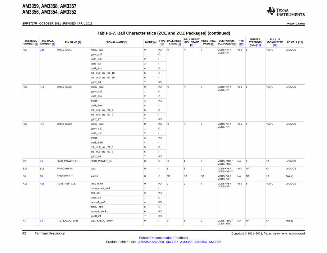
AM3359, AM3358, AM3357AM3356, AM3354, AM3352
SPRS717F –OCTOBER 2011–REVISED APRIL 2013 www.ti.com
Table 2-7. Ball Characteristics (ZCE and ZCZ Packages) (continued)BALL RESET BUFFER PULLUPZCE BALL ZCZ BALL TYPE BALL RESET RESET REL. ZCE POWER / HYSPIN NAME [2] SIGNAL NAME [3] MODE [4] REL. STATE STRENGTH /DOWN TYPE I/O CELL [13]NUMBER [1] NUMBER [1] [5] STATE [6] MODE [8] ZCZ POWER [9] [10][7] (mA) [11] [12]
H17 G15 MMC0_DAT1 mmc0_dat1 0 I/O H H 7 VDDSHV4 / Yes 6 PU/PD LVCMOSVDDSHV4
gpmc_a22 1 O
uart5_ctsn 2 I
uart3_rxd 3 I
uart1_dtrn 4 O
pr1_pru0_pru_r30_10 5 O
pr1_pru0_pru_r31_10 6 I
gpio2_28 7 I/O
H18 F18 MMC0_DAT2 mmc0_dat2 0 I/O H H 7 VDDSHV4 / Yes 6 PU/PD LVCMOSVDDSHV4
gpmc_a21 1 O
uart4_rtsn 2 O
timer6 3 I/O
uart1_dsrn 4 I
pr1_pru0_pru_r30_9 5 O
pr1_pru0_pru_r31_9 6 I
gpio2_27 7 I/O
H19 F17 MMC0_DAT3 mmc0_dat3 0 I/O H H 7 VDDSHV4 / Yes 6 PU/PD LVCMOSVDDSHV4
gpmc_a20 1 O
uart4_ctsn 2 I
timer5 3 I/O
uart1_dcdn 4 I
pr1_pru0_pru_r30_8 5 O
pr1_pru0_pru_r31_8 6 I
gpio2_26 7 I/O
C7 C6 PMIC_POWER_EN PMIC_POWER_EN 0 O H 1 0 VDDS_RTC / NA 6 NA LVCMOSVDDS_RTC
E15 B15 PWRONRSTn porz 0 I Z Z 0 VDDSHV6 / Yes NA NA LVCMOSVDDSHV6 (11)
B6 A3 RESERVED (3) testout 0 O NA NA NA VDDSHV6 / NA NA NA AnalogVDDSHV6
K18 H18 RMII1_REF_CLK rmii1_refclk 0 I/O L L 7 VDDSHV5 / Yes 6 PU/PD LVCMOSVDDSHV5
xdma_event_intr2 1 I
spi1_cs0 2 I/O
uart5_txd 3 O
mcasp1_axr3 4 I/O
mmc0_pow 5 O
mcasp1_ahclkx 6 I/O
gpio0_29 7 I/O
A7 B4 RTC_KALDO_ENn ENZ_KALDO_1P8V 0 I Z Z 0 VDDS_RTC / NA NA NA AnalogVDDS_RTC
42 Terminal Description Copyright © 2011–2013, Texas Instruments Incorporated
Submit Documentation FeedbackProduct Folder Links: AM3359 AM3358 AM3357 AM3356 AM3354 AM3352

AM3359, AM3358, AM3357AM3356, AM3354, AM3352
www.ti.com SPRS717F –OCTOBER 2011–REVISED APRIL 2013
Table 2-7. Ball Characteristics (ZCE and ZCZ Packages) (continued)BALL RESET BUFFER PULLUPZCE BALL ZCZ BALL TYPE BALL RESET RESET REL. ZCE POWER / HYSPIN NAME [2] SIGNAL NAME [3] MODE [4] REL. STATE STRENGTH /DOWN TYPE I/O CELL [13]NUMBER [1] NUMBER [1] [5] STATE [6] MODE [8] ZCZ POWER [9] [10][7] (mA) [11] [12]
B7 B5 RTC_PWRONRSTn RTC_PORz 0 I Z Z 0 VDDS_RTC / Yes NA NA LVCMOSVDDS_RTC
A6 A6 RTC_XTALIN OSC1_IN 0 I H H 0 VDDS_RTC / Yes NA PU (1) LVCMOSVDDS_RTC
A5 A4 RTC_XTALOUT OSC1_OUT 0 O Z (22) Z (22) 0 VDDS_RTC / NA NA (14) NA LVCMOSVDDS_RTC
A18 A17 SPI0_SCLK spi0_sclk 0 I/O Z H 7 VDDSHV6 / Yes 6 PU/PD LVCMOSVDDSHV6
uart2_rxd 1 I
I2C2_SDA 2 I/OD
ehrpwm0A 3 O
pr1_uart0_cts_n 4 I
pr1_edio_sof 5 O
EMU2 6 I/O
gpio0_2 7 I/O
A17 A16 SPI0_CS0 spi0_cs0 0 I/O Z H 7 VDDSHV6 / Yes 6 PU/PD LVCMOSVDDSHV6
mmc2_sdwp 1 I
I2C1_SCL 2 I/OD
ehrpwm0_synci 3 I
pr1_uart0_txd 4 O
pr1_edio_data_in1 5 I
pr1_edio_data_out1 6 O
gpio0_5 7 I/O
B16 C15 SPI0_CS1 spi0_cs1 0 I/O Z H 7 VDDSHV6 / Yes 6 PU/PD LVCMOSVDDSHV6
uart3_rxd 1 I
eCAP1_in_PWM1_out 2 I/O
mmc0_pow 3 O
xdma_event_intr2 4 I
mmc0_sdcd 5 I
EMU4 6 I/O
gpio0_6 7 I/O
B18 B17 SPI0_D0 spi0_d0 0 I/O Z H 7 VDDSHV6 / Yes 6 PU/PD LVCMOSVDDSHV6
uart2_txd 1 O
I2C2_SCL 2 I/OD
ehrpwm0B 3 O
pr1_uart0_rts_n 4 O
pr1_edio_latch_in 5 I
EMU3 6 I/O
gpio0_3 7 I/O
Copyright © 2011–2013, Texas Instruments Incorporated Terminal Description 43Submit Documentation Feedback
Product Folder Links: AM3359 AM3358 AM3357 AM3356 AM3354 AM3352
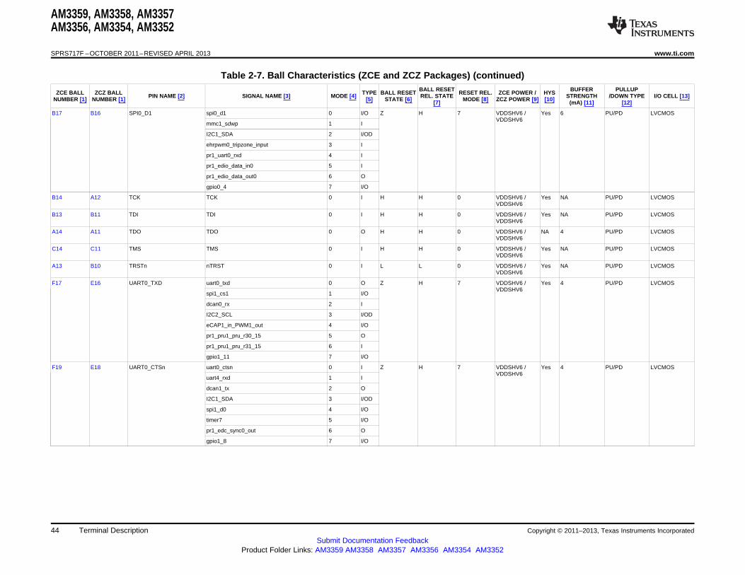
AM3359, AM3358, AM3357AM3356, AM3354, AM3352
SPRS717F –OCTOBER 2011–REVISED APRIL 2013 www.ti.com
Table 2-7. Ball Characteristics (ZCE and ZCZ Packages) (continued)BALL RESET BUFFER PULLUPZCE BALL ZCZ BALL TYPE BALL RESET RESET REL. ZCE POWER / HYSPIN NAME [2] SIGNAL NAME [3] MODE [4] REL. STATE STRENGTH /DOWN TYPE I/O CELL [13]NUMBER [1] NUMBER [1] [5] STATE [6] MODE [8] ZCZ POWER [9] [10][7] (mA) [11] [12]
B17 B16 SPI0_D1 spi0_d1 0 I/O Z H 7 VDDSHV6 / Yes 6 PU/PD LVCMOSVDDSHV6
mmc1_sdwp 1 I
I2C1_SDA 2 I/OD
ehrpwm0_tripzone_input 3 I
pr1_uart0_rxd 4 I
pr1_edio_data_in0 5 I
pr1_edio_data_out0 6 O
gpio0_4 7 I/O
B14 A12 TCK TCK 0 I H H 0 VDDSHV6 / Yes NA PU/PD LVCMOSVDDSHV6
B13 B11 TDI TDI 0 I H H 0 VDDSHV6 / Yes NA PU/PD LVCMOSVDDSHV6
A14 A11 TDO TDO 0 O H H 0 VDDSHV6 / NA 4 PU/PD LVCMOSVDDSHV6
C14 C11 TMS TMS 0 I H H 0 VDDSHV6 / Yes NA PU/PD LVCMOSVDDSHV6
A13 B10 TRSTn nTRST 0 I L L 0 VDDSHV6 / Yes NA PU/PD LVCMOSVDDSHV6
F17 E16 UART0_TXD uart0_txd 0 O Z H 7 VDDSHV6 / Yes 4 PU/PD LVCMOSVDDSHV6
spi1_cs1 1 I/O
dcan0_rx 2 I
I2C2_SCL 3 I/OD
eCAP1_in_PWM1_out 4 I/O
pr1_pru1_pru_r30_15 5 O
pr1_pru1_pru_r31_15 6 I
gpio1_11 7 I/O
F19 E18 UART0_CTSn uart0_ctsn 0 I Z H 7 VDDSHV6 / Yes 4 PU/PD LVCMOSVDDSHV6
uart4_rxd 1 I
dcan1_tx 2 O
I2C1_SDA 3 I/OD
spi1_d0 4 I/O
timer7 5 I/O
pr1_edc_sync0_out 6 O
gpio1_8 7 I/O
44 Terminal Description Copyright © 2011–2013, Texas Instruments Incorporated
Submit Documentation FeedbackProduct Folder Links: AM3359 AM3358 AM3357 AM3356 AM3354 AM3352

AM3359, AM3358, AM3357AM3356, AM3354, AM3352
www.ti.com SPRS717F –OCTOBER 2011–REVISED APRIL 2013
Table 2-7. Ball Characteristics (ZCE and ZCZ Packages) (continued)BALL RESET BUFFER PULLUPZCE BALL ZCZ BALL TYPE BALL RESET RESET REL. ZCE POWER / HYSPIN NAME [2] SIGNAL NAME [3] MODE [4] REL. STATE STRENGTH /DOWN TYPE I/O CELL [13]NUMBER [1] NUMBER [1] [5] STATE [6] MODE [8] ZCZ POWER [9] [10][7] (mA) [11] [12]
E19 E15 UART0_RXD uart0_rxd 0 I Z H 7 VDDSHV6 / Yes 4 PU/PD LVCMOSVDDSHV6
spi1_cs0 1 I/O
dcan0_tx 2 O
I2C2_SDA 3 I/OD
eCAP2_in_PWM2_out 4 I/O
pr1_pru1_pru_r30_14 5 O
pr1_pru1_pru_r31_14 6 I
gpio1_10 7 I/O
F18 E17 UART0_RTSn uart0_rtsn 0 O Z H 7 VDDSHV6 / Yes 4 PU/PD LVCMOSVDDSHV6
uart4_txd 1 O
dcan1_rx 2 I
I2C1_SCL 3 I/OD
spi1_d1 4 I/O
spi1_cs0 5 I/O
pr1_edc_sync1_out 6 O
gpio1_9 7 I/O
C19 D15 UART1_TXD uart1_txd 0 O Z H 7 VDDSHV6 / Yes 4 PU/PD LVCMOSVDDSHV6
mmc2_sdwp 1 I
dcan1_rx 2 I
I2C1_SCL 3 I/OD
pr1_uart0_txd 5 O
pr1_pru0_pru_r31_16 6 I
gpio0_15 7 I/O
D18 D16 UART1_RXD uart1_rxd 0 I Z H 7 VDDSHV6 / Yes 4 PU/PD LVCMOSVDDSHV6
mmc1_sdwp 1 I
dcan1_tx 2 O
I2C1_SDA 3 I/OD
pr1_uart0_rxd 5 I
pr1_pru1_pru_r31_16 6 I
gpio0_14 7 I/O
D19 D17 UART1_RTSn uart1_rtsn 0 O Z H 7 VDDSHV6 / Yes 4 PU/PD LVCMOSVDDSHV6
timer5 1 I/O
dcan0_rx 2 I
I2C2_SCL 3 I/OD
spi1_cs1 4 I/O
pr1_uart0_rts_n 5 O
pr1_edc_latch1_in 6 I
gpio0_13 7 I/O
Copyright © 2011–2013, Texas Instruments Incorporated Terminal Description 45Submit Documentation Feedback
Product Folder Links: AM3359 AM3358 AM3357 AM3356 AM3354 AM3352
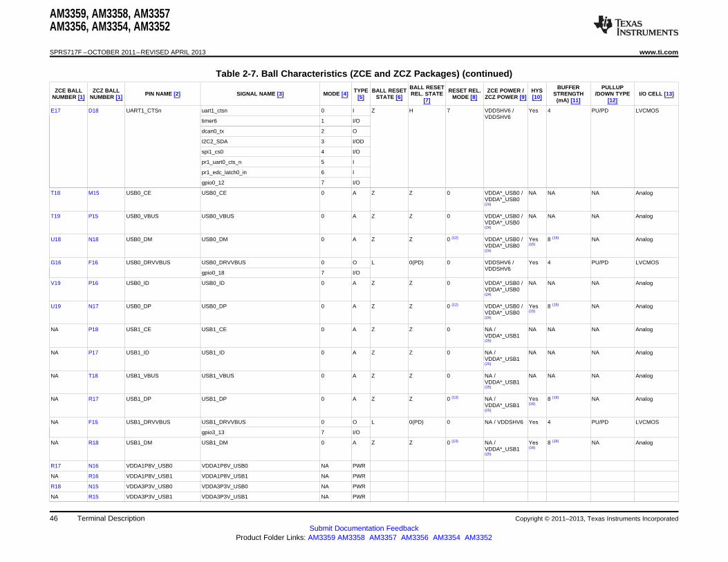
AM3359, AM3358, AM3357AM3356, AM3354, AM3352
SPRS717F –OCTOBER 2011–REVISED APRIL 2013 www.ti.com
Table 2-7. Ball Characteristics (ZCE and ZCZ Packages) (continued)BALL RESET BUFFER PULLUPZCE BALL ZCZ BALL TYPE BALL RESET RESET REL. ZCE POWER / HYSPIN NAME [2] SIGNAL NAME [3] MODE [4] REL. STATE STRENGTH /DOWN TYPE I/O CELL [13]NUMBER [1] NUMBER [1] [5] STATE [6] MODE [8] ZCZ POWER [9] [10][7] (mA) [11] [12]
E17 D18 UART1_CTSn uart1_ctsn 0 I Z H 7 VDDSHV6 / Yes 4 PU/PD LVCMOSVDDSHV6
timer6 1 I/O
dcan0_tx 2 O
I2C2_SDA 3 I/OD
spi1_cs0 4 I/O
pr1_uart0_cts_n 5 I
pr1_edc_latch0_in 6 I
gpio0_12 7 I/O
T18 M15 USB0_CE USB0_CE 0 A Z Z 0 VDDA*_USB0 / NA NA NA AnalogVDDA*_USB0(24)
T19 P15 USB0_VBUS USB0_VBUS 0 A Z Z 0 VDDA*_USB0 / NA NA NA AnalogVDDA*_USB0(24)
U18 N18 USB0_DM USB0_DM 0 A Z Z 0 (12) VDDA*_USB0 / Yes 8 (15) NA AnalogVDDA*_USB0 (15)
(24)
G16 F16 USB0_DRVVBUS USB0_DRVVBUS 0 O L 0(PD) 0 VDDSHV6 / Yes 4 PU/PD LVCMOSVDDSHV6
gpio0_18 7 I/O
V19 P16 USB0_ID USB0_ID 0 A Z Z 0 VDDA*_USB0 / NA NA NA AnalogVDDA*_USB0(24)
U19 N17 USB0_DP USB0_DP 0 A Z Z 0 (12) VDDA*_USB0 / Yes 8 (15) NA AnalogVDDA*_USB0 (15)
(24)
NA P18 USB1_CE USB1_CE 0 A Z Z 0 NA / NA NA NA AnalogVDDA*_USB1(25)
NA P17 USB1_ID USB1_ID 0 A Z Z 0 NA / NA NA NA AnalogVDDA*_USB1(25)
NA T18 USB1_VBUS USB1_VBUS 0 A Z Z 0 NA / NA NA NA AnalogVDDA*_USB1(25)
NA R17 USB1_DP USB1_DP 0 A Z Z 0 (13) NA / Yes 8 (16) NA AnalogVDDA*_USB1 (16)
(25)
NA F15 USB1_DRVVBUS USB1_DRVVBUS 0 O L 0(PD) 0 NA / VDDSHV6 Yes 4 PU/PD LVCMOS
gpio3_13 7 I/O
NA R18 USB1_DM USB1_DM 0 A Z Z 0 (13) NA / Yes 8 (16) NA AnalogVDDA*_USB1 (16)
(25)
R17 N16 VDDA1P8V_USB0 VDDA1P8V_USB0 NA PWR
NA R16 VDDA1P8V_USB1 VDDA1P8V_USB1 NA PWR
R18 N15 VDDA3P3V_USB0 VDDA3P3V_USB0 NA PWR
NA R15 VDDA3P3V_USB1 VDDA3P3V_USB1 NA PWR
46 Terminal Description Copyright © 2011–2013, Texas Instruments Incorporated
Submit Documentation FeedbackProduct Folder Links: AM3359 AM3358 AM3357 AM3356 AM3354 AM3352
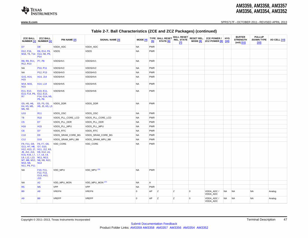
AM3359, AM3358, AM3357AM3356, AM3354, AM3352
www.ti.com SPRS717F –OCTOBER 2011–REVISED APRIL 2013
Table 2-7. Ball Characteristics (ZCE and ZCZ Packages) (continued)BALL RESET BUFFER PULLUPZCE BALL ZCZ BALL TYPE BALL RESET RESET REL. ZCE POWER / HYSPIN NAME [2] SIGNAL NAME [3] MODE [4] REL. STATE STRENGTH /DOWN TYPE I/O CELL [13]NUMBER [1] NUMBER [1] [5] STATE [6] MODE [8] ZCZ POWER [9] [10][7] (mA) [11] [12]
D7 D8 VDDA_ADC VDDA_ADC NA PWR
D12, F16, E6, E14, F9, VDDS VDDS NA PWRM16, T6, T14 K13, N6, P9,
P14
R8, R9, R11, P7, P8 VDDSHV1 VDDSHV1 NA PWRR12, R13
NA P10, P11 VDDSHV2 VDDSHV2 NA PWR
NA P12, P13 VDDSHV3 VDDSHV3 NA PWR
G15, H14, H14, J14 VDDSHV4 VDDSHV4 NA PWRH15
M14, M15, K14, L14 VDDSHV5 VDDSHV5 NA PWRN15
E11, E12, E10, E11, VDDSHV6 VDDSHV6 NA PWRE13, F14, P6, E12, E13,R7 F14, G14, N5,
P5, P6
G5, H5, H6, E5, F5, G5, VDDS_DDR VDDS_DDR NA PWRK4, K5, M5, H5, J5, K5, L5M6, N5
U10 R11 VDDS_OSC VDDS_OSC NA PWR
T8 R10 VDDS_PLL_CORE_LCD VDDS_PLL_CORE_LCD NA PWR
C5 E7 VDDS_PLL_DDR VDDS_PLL_DDR NA PWR
H16 H15 VDDS_PLL_MPU VDDS_PLL_MPU NA PWR
C6 D7 VDDS_RTC VDDS_RTC NA PWR
C10 E9 VDDS_SRAM_CORE_BG VDDS_SRAM_CORE_BG NA PWR
C12 D10 VDDS_SRAM_MPU_BB VDDS_SRAM_MPU_BB NA PWR
F9, F11, G9, F6, F7, G6, VDD_CORE VDD_CORE NA PWRG11, H7, H8, G7, G10,H12, H13, J7, H11, J12, K6,J8, J12, J13, K8, K12, L6,K15, K16, L7, L7, L8, L9,L8, L12, L13, M11, M13,M7, M8, M12, N8, N9, N12,M13, N9, N13N11, P9, P11
NA F10, F11, VDD_MPU VDD_MPU (26) NA PWRF12, F13,G13, H13,J13
NA A2 VDD_MPU_MON VDD_MPU_MON (27) NA A
R5 M5 VPP VPP NA PWR
B9 A9 VREFN VREFN 0 AP Z Z 0 VDDA_ADC / NA NA NA AnalogVDDA_ADC
A9 B9 VREFP VREFP 0 AP Z Z 0 VDDA_ADC / NA NA NA AnalogVDDA_ADC
Copyright © 2011–2013, Texas Instruments Incorporated Terminal Description 47Submit Documentation Feedback
Product Folder Links: AM3359 AM3358 AM3357 AM3356 AM3354 AM3352
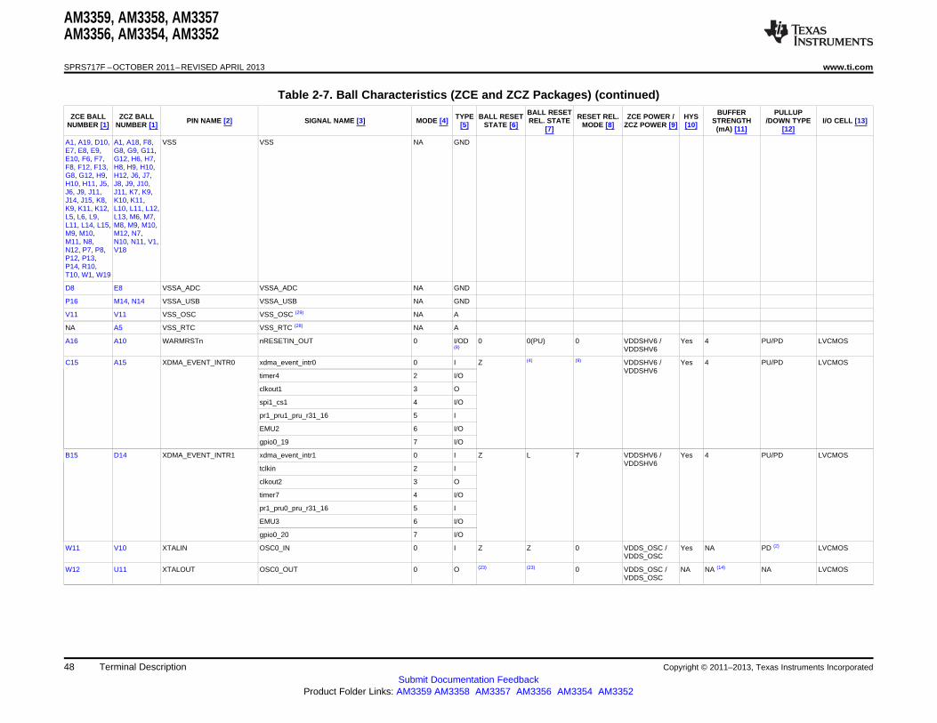
AM3359, AM3358, AM3357AM3356, AM3354, AM3352
SPRS717F –OCTOBER 2011–REVISED APRIL 2013 www.ti.com
Table 2-7. Ball Characteristics (ZCE and ZCZ Packages) (continued)BALL RESET BUFFER PULLUPZCE BALL ZCZ BALL TYPE BALL RESET RESET REL. ZCE POWER / HYSPIN NAME [2] SIGNAL NAME [3] MODE [4] REL. STATE STRENGTH /DOWN TYPE I/O CELL [13]NUMBER [1] NUMBER [1] [5] STATE [6] MODE [8] ZCZ POWER [9] [10][7] (mA) [11] [12]
A1, A19, D10, A1, A18, F8, VSS VSS NA GNDE7, E8, E9, G8, G9, G11,E10, F6, F7, G12, H6, H7,F8, F12, F13, H8, H9, H10,G8, G12, H9, H12, J6, J7,H10, H11, J5, J8, J9, J10,J6, J9, J11, J11, K7, K9,J14, J15, K8, K10, K11,K9, K11, K12, L10, L11, L12,L5, L6, L9, L13, M6, M7,L11, L14, L15, M8, M9, M10,M9, M10, M12, N7,M11, N8, N10, N11, V1,N12, P7, P8, V18P12, P13,P14, R10,T10, W1, W19
D8 E8 VSSA_ADC VSSA_ADC NA GND
P16 M14, N14 VSSA_USB VSSA_USB NA GND
V11 V11 VSS_OSC VSS_OSC (29) NA A
NA A5 VSS_RTC VSS_RTC (28) NA A
A16 A10 WARMRSTn nRESETIN_OUT 0 I/OD 0 0(PU) 0 VDDSHV6 / Yes 4 PU/PD LVCMOS(8) VDDSHV6
C15 A15 XDMA_EVENT_INTR0 xdma_event_intr0 0 I Z (4) (9) VDDSHV6 / Yes 4 PU/PD LVCMOSVDDSHV6
timer4 2 I/O
clkout1 3 O
spi1_cs1 4 I/O
pr1_pru1_pru_r31_16 5 I
EMU2 6 I/O
gpio0_19 7 I/O
B15 D14 XDMA_EVENT_INTR1 xdma_event_intr1 0 I Z L 7 VDDSHV6 / Yes 4 PU/PD LVCMOSVDDSHV6
tclkin 2 I
clkout2 3 O
timer7 4 I/O
pr1_pru0_pru_r31_16 5 I
EMU3 6 I/O
gpio0_20 7 I/O
W11 V10 XTALIN OSC0_IN 0 I Z Z 0 VDDS_OSC / Yes NA PD (2) LVCMOSVDDS_OSC
W12 U11 XTALOUT OSC0_OUT 0 O (23) (23) 0 VDDS_OSC / NA NA (14) NA LVCMOSVDDS_OSC
48 Terminal Description Copyright © 2011–2013, Texas Instruments Incorporated
Submit Documentation FeedbackProduct Folder Links: AM3359 AM3358 AM3357 AM3356 AM3354 AM3352

AM3359, AM3358, AM3357AM3356, AM3354, AM3352
www.ti.com SPRS717F –OCTOBER 2011–REVISED APRIL 2013
(1) An internal 10 kohm pull up is turned on when the oscillator is diasabled. The oscillator is disabled by default after power is applied.
(2) An internal 15 kohm pull down is turned on when the oscillator is disabled. The oscillator is enabled by default after power is applied.
(3) Do not connect anything to this terminal.
(4) If sysboot[5] is low on the rising edge of PWRONRSTn, this terminal has an internal pull-down turned on after reset is released. If sysboot[5] is high on the rising edge or PWRONRSTn,this terminal will initially be driven low after reset is released then it begins to toggle at the same frequency of the XTALIN terminal.
(5) LCD_DATA[15:0] terminals are respectively SYSBOOT[15:0] inputs, latched on the rising edge of PWRONRSTn.
(6) Mode1 and Mode2 signal assignments for this terminal are only available with silicon revision 2.0 or newer devices.
(7) Mode2 signal assignment for this terminal is only available with silicon revision 2.0 or newer devices.
(8) Refer to the External Warm Reset section of the AM335x Technical Reference Manual for more information related to the operation of this terminal.
(9) Reset Release Mode = 7 if sysboot[5] is low. Mode = 3 if sysboot[5] is high.
(10) Silicon revision 1.0 devices only provide the MMC2_DAT7 signal when Mode3 is selected. Silicon revision 2.0 and newer devices implement another level of pin multiplexing whichprovides the original MMC2_DAT7 signal or RMII2_CRS_DV signal when Mode3 is selected. This new level of of pin multiplexing is selected with bit zero of the SMA2 register. For moredetails refer to Section 1.2 of the AM335x Technical Reference Manual.
(11) The input voltage thresholds for this input are not a function of VDDSHV6. Please refer to the DC Electrical Characteristics section for details related to electrical parameters associatedwith this input terminal.
(12) The internal USB PHY can be configured to multiplex the UART2_TX or UART2_RX signals to this terminal. For more details refer to USB GPIO Details section of the AM335x TechnicalReference Manual.
(13) The internal USB PHY can be configured to multiplex the UART3_TX or UART3_RX signals to this terminal. For more details refer to USB GPIO Details section of the AM335x TechnicalReference Manual.
(14) This output should only be used to source the recommended crystal circuit.
(15) This parameter only applies when this USB PHY terminal is operating in UART2 mode.
(16) This parameter only applies when this USB PHY terminal is operating in UART3 mode.
(17) This terminal is a analog input used to set the switching threshold of the DDR input buffers to (VDDS_DDR / 2).
(18) This terminal is a analog passive signal that connects to an external 49.9 ohm 1%, 20mW reference resistor which is used to calibrate the DDR input/output buffers.
(19) This terminal is analog input that may also be configured as an open-drain output.
(20) This terminal is analog input that may also be configured as an open-source or open-drain output.
(21) This terminal is analog input that may also be configured as an open-source output.
(22) This terminal is high-Z when the oscillator is diasabled. This terminal is driven high if RTC_XTALIN is less than VIL, driven low if RTC_XTALIN is greater than VIH, and driven to aunknown value if RTC_XTALIN is between VIL and VIH when the oscillator is enabled. The oscillator is disabled by default after power is applied.
(23) This terminal is high-Z when the oscillator is diasabled. This terminal is driven high if XTALIN is less than VIL, driven low if XTALIN is greater than VIH, and driven to a unknown value ifXTALIN is between VIL and VIH when the oscillator is enabled. The oscillator is enabled by default after power is applied.
(24) This terminal requires two power supplies, VDDA3p3v_USB0 and VDDA1p8v_USB0. The "*" character in the power supply name is a wild card that represents "3p3v" and "1p8v".
(25) This terminal requires two power supplies, VDDA3p3v_USB1 and VDDA1p8v_USB1. The "*" character in the power supply name is a wild card that represents "3p3v" and "1p8v".
(26) This power rail is connected to VDD_CORE in the ZCE package.
(27) This terminal provides a Kelvin connection to VDD_MPU. It can be connected to the power supply feedback input to provide remote sensing which compensates for voltage drop in thePCB power distribution network and package. When the Kelvin connection is not used it should be connected to the same power source as VDD_MPU.
(28) This terminal provides a Kelvin ground reference for the external crystal components. If a crystal circuit is connected to the RTC_XTALIN/RTC_XTALOUT terminals, the crystal circuitcomponent grounds should only be connected to this terminal and should not be connected to the PCB ground plane. If an external LVCMOS clock source is connected to the XTALINterminal, this terminal should be connected to VSS.
(29) This terminal provides a Kelvin ground reference for the external crystal components. If a crystal circuit is connected to the XTALIN/XTALOUT terminals, the crystal circuit component
Copyright © 2011–2013, Texas Instruments Incorporated Terminal Description 49Submit Documentation Feedback
Product Folder Links: AM3359 AM3358 AM3357 AM3356 AM3354 AM3352

AM3359, AM3358, AM3357AM3356, AM3354, AM3352
SPRS717F –OCTOBER 2011–REVISED APRIL 2013 www.ti.com
grounds should only be connected to this terminal and should not be connected to the PCB ground plane. If an external LVCMOS clock source is connected to the XTALIN terminal, thisterminal should be connected to VSS.
50 Terminal Description Copyright © 2011–2013, Texas Instruments Incorporated
Submit Documentation FeedbackProduct Folder Links: AM3359 AM3358 AM3357 AM3356 AM3354 AM3352
AM3359, AM3358, AM3357AM3356, AM3354, AM3352
www.ti.com SPRS717F –OCTOBER 2011–REVISED APRIL 2013
2.3 Signal Description
The AM335x device contains many peripheral interfaces. In order to reduce package size and loweroverall system cost while maintaining maximum functionality, many of the AM335x terminals can multiplexup to eight signal functions. Although there are many combinations of pin multiplexing that are possible,only a certain number of sets, called IO Sets, are valid due to timing limitations. These valid IO Sets werecarefully chosen to provide many possible application scenarios for the user.
Texas Instruments has developed a Windows-based application called Pin Mux Utility that helps a systemdesigner select the appropriate pin-multiplexing configuration for their AM335x-based product design. ThePin Mux Utility provides a way to select valid IO Sets of specific peripheral interfaces to ensure the pin-multiplexing configuration selected for a design only uses valid IO Sets supported by the AM335x device.
Copyright © 2011–2013, Texas Instruments Incorporated Terminal Description 51Submit Documentation Feedback
Product Folder Links: AM3359 AM3358 AM3357 AM3356 AM3354 AM3352

AM3359, AM3358, AM3357AM3356, AM3354, AM3352
SPRS717F –OCTOBER 2011–REVISED APRIL 2013 www.ti.com
(1) SIGNAL NAME: The signal name
(2) DESCRIPTION: Description of the signal
(3) TYPE: Ball type for this specific function:
– I = Input– O = Output– I/O = Input/Output– D = Open drain– DS = Differential– A = Analog
(4) BALL: Package ball location
Table 2-8. ADC Signals Description
TYPESIGNAL NAME [1] DESCRIPTION [2] ZCE BALL [4] ZCZ BALL [4][3]
AIN0 Analog Input/Output A B8 B6
AIN1 Analog Input/Output A A11 C7
AIN2 Analog Input/Output A A8 B7
AIN3 Analog Input/Output A B11 A7
AIN4 Analog Input/Output A C8 C8
AIN5 Analog Input A B12 B8
AIN6 Analog Input A A10 A8
AIN7 Analog Input A A12 C9
VREFN Analog Negative Reference Input AP B9 A9
VREFP Analog Positive Reference Input AP A9 B9
Table 2-9. Debug Subsystem Signals Description
TYPESIGNAL NAME [1] DESCRIPTION [2] ZCE BALL [4] ZCZ BALL [4][3]
EMU0 MISC EMULATION PIN I/O A15 C14
EMU1 MISC EMULATION PIN I/O D14 B14
EMU2 MISC EMULATION PIN I/O A18, C15 A15, A17, C13
EMU3 MISC EMULATION PIN I/O B15, B18 B17, D13, D14
EMU4 MISC EMULATION PIN I/O B16, U17 A14, C15, T13
nTRST JTAG TEST RESET (ACTIVE LOW) I A13 B10
TCK JTAG TEST CLOCK I B14 A12
TDI JTAG TEST DATA INPUT I B13 B11
TDO JTAG TEST DATA OUTPUT O A14 A11
TMS JTAG TEST MODE SELECT I C14 C11
Table 2-10. LCD Controller Signals Description
TYPESIGNAL NAME [1] DESCRIPTION [2] ZCE BALL [4] ZCZ BALL [4][3]
lcd_ac_bias_en LCD AC bias enable chip select O W7 R6
lcd_data0 LCD data bus I/O U1 R1
lcd_data1 LCD data bus I/O U2 R2
lcd_data10 LCD data bus I/O U5 U3
lcd_data11 LCD data bus I/O V5 U4
lcd_data12 LCD data bus I/O V6 V2
lcd_data13 LCD data bus I/O U6 V3
lcd_data14 LCD data bus I/O W6 V4
lcd_data15 LCD data bus I/O V7 T5
lcd_data16 LCD data bus O V17 U13
52 Terminal Description Copyright © 2011–2013, Texas Instruments Incorporated
Submit Documentation FeedbackProduct Folder Links: AM3359 AM3358 AM3357 AM3356 AM3354 AM3352
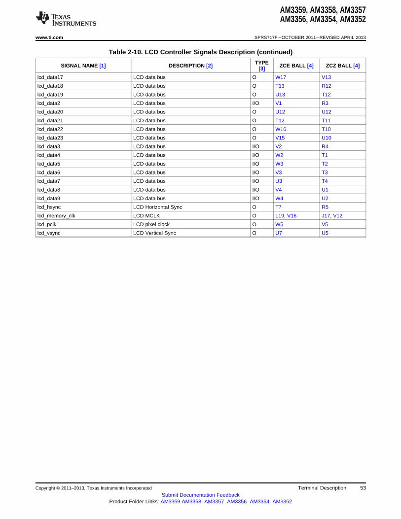
AM3359, AM3358, AM3357AM3356, AM3354, AM3352
www.ti.com SPRS717F –OCTOBER 2011–REVISED APRIL 2013
Table 2-10. LCD Controller Signals Description (continued)
TYPESIGNAL NAME [1] DESCRIPTION [2] ZCE BALL [4] ZCZ BALL [4][3]
lcd_data17 LCD data bus O W17 V13
lcd_data18 LCD data bus O T13 R12
lcd_data19 LCD data bus O U13 T12
lcd_data2 LCD data bus I/O V1 R3
lcd_data20 LCD data bus O U12 U12
lcd_data21 LCD data bus O T12 T11
lcd_data22 LCD data bus O W16 T10
lcd_data23 LCD data bus O V15 U10
lcd_data3 LCD data bus I/O V2 R4
lcd_data4 LCD data bus I/O W2 T1
lcd_data5 LCD data bus I/O W3 T2
lcd_data6 LCD data bus I/O V3 T3
lcd_data7 LCD data bus I/O U3 T4
lcd_data8 LCD data bus I/O V4 U1
lcd_data9 LCD data bus I/O W4 U2
lcd_hsync LCD Horizontal Sync O T7 R5
lcd_memory_clk LCD MCLK O L19, V16 J17, V12
lcd_pclk LCD pixel clock O W5 V5
lcd_vsync LCD Vertical Sync O U7 U5
Copyright © 2011–2013, Texas Instruments Incorporated Terminal Description 53Submit Documentation Feedback
Product Folder Links: AM3359 AM3358 AM3357 AM3356 AM3354 AM3352
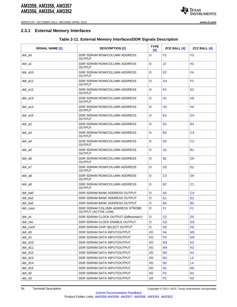
AM3359, AM3358, AM3357AM3356, AM3354, AM3352
SPRS717F –OCTOBER 2011–REVISED APRIL 2013 www.ti.com
2.3.1 External Memory Interfaces
Table 2-11. External Memory Interfaces/DDR Signals Description
TYPESIGNAL NAME [1] DESCRIPTION [2] ZCE BALL [4] ZCZ BALL [4][3]
ddr_a0 DDR SDRAM ROW/COLUMN ADDRESS O F3 F3OUTPUT
ddr_a1 DDR SDRAM ROW/COLUMN ADDRESS O J2 H1OUTPUT
ddr_a10 DDR SDRAM ROW/COLUMN ADDRESS O E2 F4OUTPUT
ddr_a11 DDR SDRAM ROW/COLUMN ADDRESS O G4 F2OUTPUT
ddr_a12 DDR SDRAM ROW/COLUMN ADDRESS O F4 E3OUTPUT
ddr_a13 DDR SDRAM ROW/COLUMN ADDRESS O H1 H3OUTPUT
ddr_a14 DDR SDRAM ROW/COLUMN ADDRESS O H3 H4OUTPUT
ddr_a15 DDR SDRAM ROW/COLUMN ADDRESS O E3 D3OUTPUT
ddr_a2 DDR SDRAM ROW/COLUMN ADDRESS O D1 E4OUTPUT
ddr_a3 DDR SDRAM ROW/COLUMN ADDRESS O B3 C3OUTPUT
ddr_a4 DDR SDRAM ROW/COLUMN ADDRESS O E5 C2OUTPUT
ddr_a5 DDR SDRAM ROW/COLUMN ADDRESS O A2 B1OUTPUT
ddr_a6 DDR SDRAM ROW/COLUMN ADDRESS O B1 D5OUTPUT
ddr_a7 DDR SDRAM ROW/COLUMN ADDRESS O D2 E2OUTPUT
ddr_a8 DDR SDRAM ROW/COLUMN ADDRESS O C3 D4OUTPUT
ddr_a9 DDR SDRAM ROW/COLUMN ADDRESS O B2 C1OUTPUT
ddr_ba0 DDR SDRAM BANK ADDRESS OUTPUT O A3 C4
ddr_ba1 DDR SDRAM BANK ADDRESS OUTPUT O E1 E1
ddr_ba2 DDR SDRAM BANK ADDRESS OUTPUT O B4 B3
ddr_casn DDR SDRAM COLUMN ADDRESS STROBE O F1 F1OUTPUT (ACTIVE LOW)
ddr_ck DDR SDRAM CLOCK OUTPUT (Differential+) O C2 D2
ddr_cke DDR SDRAM CLOCK ENABLE OUTPUT O G3 G3
ddr_csn0 DDR SDRAM CHIP SELECT OUTPUT O H2 H2
ddr_d0 DDR SDRAM DATA INPUT/OUTPUT I/O N4 M3
ddr_d1 DDR SDRAM DATA INPUT/OUTPUT I/O P4 M4
ddr_d10 DDR SDRAM DATA INPUT/OUTPUT I/O M3 K2
ddr_d11 DDR SDRAM DATA INPUT/OUTPUT I/O M4 K3
ddr_d12 DDR SDRAM DATA INPUT/OUTPUT I/O M2 K4
ddr_d13 DDR SDRAM DATA INPUT/OUTPUT I/O M1 L3
ddr_d14 DDR SDRAM DATA INPUT/OUTPUT I/O N2 L4
ddr_d15 DDR SDRAM DATA INPUT/OUTPUT I/O N1 M1
ddr_d2 DDR SDRAM DATA INPUT/OUTPUT I/O P2 N1
ddr_d3 DDR SDRAM DATA INPUT/OUTPUT I/O P1 N2
54 Terminal Description Copyright © 2011–2013, Texas Instruments Incorporated
Submit Documentation FeedbackProduct Folder Links: AM3359 AM3358 AM3357 AM3356 AM3354 AM3352
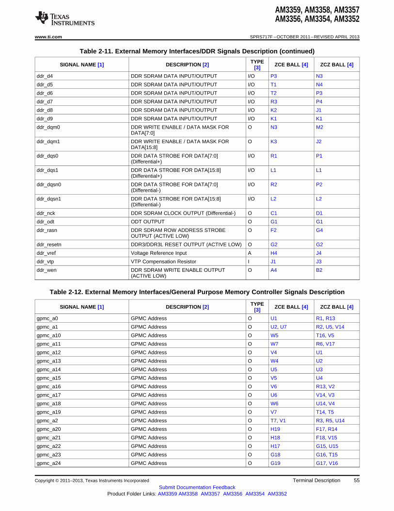
AM3359, AM3358, AM3357AM3356, AM3354, AM3352
www.ti.com SPRS717F –OCTOBER 2011–REVISED APRIL 2013
Table 2-11. External Memory Interfaces/DDR Signals Description (continued)
TYPESIGNAL NAME [1] DESCRIPTION [2] ZCE BALL [4] ZCZ BALL [4][3]
ddr_d4 DDR SDRAM DATA INPUT/OUTPUT I/O P3 N3
ddr_d5 DDR SDRAM DATA INPUT/OUTPUT I/O T1 N4
ddr_d6 DDR SDRAM DATA INPUT/OUTPUT I/O T2 P3
ddr_d7 DDR SDRAM DATA INPUT/OUTPUT I/O R3 P4
ddr_d8 DDR SDRAM DATA INPUT/OUTPUT I/O K2 J1
ddr_d9 DDR SDRAM DATA INPUT/OUTPUT I/O K1 K1
ddr_dqm0 DDR WRITE ENABLE / DATA MASK FOR O N3 M2DATA[7:0]
ddr_dqm1 DDR WRITE ENABLE / DATA MASK FOR O K3 J2DATA[15:8]
ddr_dqs0 DDR DATA STROBE FOR DATA[7:0] I/O R1 P1(Differential+)
ddr_dqs1 DDR DATA STROBE FOR DATA[15:8] I/O L1 L1(Differential+)
ddr_dqsn0 DDR DATA STROBE FOR DATA[7:0] I/O R2 P2(Differential-)
ddr_dqsn1 DDR DATA STROBE FOR DATA[15:8] I/O L2 L2(Differential-)
ddr_nck DDR SDRAM CLOCK OUTPUT (Differential-) O C1 D1
ddr_odt ODT OUTPUT O G1 G1
ddr_rasn DDR SDRAM ROW ADDRESS STROBE O F2 G4OUTPUT (ACTIVE LOW)
ddr_resetn DDR3/DDR3L RESET OUTPUT (ACTIVE LOW) O G2 G2
ddr_vref Voltage Reference Input A H4 J4
ddr_vtp VTP Compensation Resistor I J1 J3
ddr_wen DDR SDRAM WRITE ENABLE OUTPUT O A4 B2(ACTIVE LOW)
Table 2-12. External Memory Interfaces/General Purpose Memory Controller Signals Description
TYPESIGNAL NAME [1] DESCRIPTION [2] ZCE BALL [4] ZCZ BALL [4][3]
gpmc_a0 GPMC Address O U1 R1, R13
gpmc_a1 GPMC Address O U2, U7 R2, U5, V14
gpmc_a10 GPMC Address O W5 T16, V5
gpmc_a11 GPMC Address O W7 R6, V17
gpmc_a12 GPMC Address O V4 U1
gpmc_a13 GPMC Address O W4 U2
gpmc_a14 GPMC Address O U5 U3
gpmc_a15 GPMC Address O V5 U4
gpmc_a16 GPMC Address O V6 R13, V2
gpmc_a17 GPMC Address O U6 V14, V3
gpmc_a18 GPMC Address O W6 U14, V4
gpmc_a19 GPMC Address O V7 T14, T5
gpmc_a2 GPMC Address O T7, V1 R3, R5, U14
gpmc_a20 GPMC Address O H19 F17, R14
gpmc_a21 GPMC Address O H18 F18, V15
gpmc_a22 GPMC Address O H17 G15, U15
gpmc_a23 GPMC Address O G18 G16, T15
gpmc_a24 GPMC Address O G19 G17, V16
Copyright © 2011–2013, Texas Instruments Incorporated Terminal Description 55Submit Documentation Feedback
Product Folder Links: AM3359 AM3358 AM3357 AM3356 AM3354 AM3352

AM3359, AM3358, AM3357AM3356, AM3354, AM3352
SPRS717F –OCTOBER 2011–REVISED APRIL 2013 www.ti.com
Table 2-12. External Memory Interfaces/General Purpose Memory Controller SignalsDescription (continued)
TYPESIGNAL NAME [1] DESCRIPTION [2] ZCE BALL [4] ZCZ BALL [4][3]
gpmc_a25 GPMC Address O G17 G18, U16
gpmc_a26 GPMC Address O NA T16
gpmc_a27 GPMC Address O NA V17
gpmc_a3 GPMC Address O U17, V2 R4, T13, T14
gpmc_a4 GPMC Address O W2 R14, T1
gpmc_a5 GPMC Address O W3 T2, V15
gpmc_a6 GPMC Address O V3 T3, U15
gpmc_a7 GPMC Address O U3 T15, T4
gpmc_a8 GPMC Address O U7 U5, V16
gpmc_a9 GPMC Address O T7 R5, U16
gpmc_ad0 GPMC Address and Data I/O W10 U7
gpmc_ad1 GPMC Address and Data I/O V9 V7
gpmc_ad10 GPMC Address and Data I/O T12 T11
gpmc_ad11 GPMC Address and Data I/O U12 U12
gpmc_ad12 GPMC Address and Data I/O U13 T12
gpmc_ad13 GPMC Address and Data I/O T13 R12
gpmc_ad14 GPMC Address and Data I/O W17 V13
gpmc_ad15 GPMC Address and Data I/O V17 U13
gpmc_ad2 GPMC Address and Data I/O V12 R8
gpmc_ad3 GPMC Address and Data I/O W13 T8
gpmc_ad4 GPMC Address and Data I/O V13 U8
gpmc_ad5 GPMC Address and Data I/O W14 V8
gpmc_ad6 GPMC Address and Data I/O U14 R9
gpmc_ad7 GPMC Address and Data I/O W15 T9
gpmc_ad8 GPMC Address and Data I/O V15 U10
gpmc_ad9 GPMC Address and Data I/O W16 T10
gpmc_advn_ale GPMC Address Valid / Address Latch Enable O V10 R7
gpmc_be0n_cle GPMC Byte Enable 0 / Command Latch Enable O V8 T6
gpmc_be1n GPMC Byte Enable 1 O U15, V18 U18, V9
gpmc_clk GPMC Clock I/O V14, V16 U9, V12
gpmc_csn0 GPMC Chip Select O W8 V6
gpmc_csn1 GPMC Chip Select O V14 U9
gpmc_csn2 GPMC Chip Select O U15 V9
gpmc_csn3 GPMC Chip Select O U17 T13
gpmc_csn4 GPMC Chip Select O R15 T17
gpmc_csn5 GPMC Chip Select O W18 U17
gpmc_csn6 GPMC Chip Select O V18 U18
gpmc_dir GPMC Data Direction O V18 U18
gpmc_oen_ren GPMC Output / Read Enable O W9 T7
gpmc_wait0 GPMC Wait 0 I R15 T17
gpmc_wait1 GPMC Wait 1 I V16 V12
gpmc_wen GPMC Write Enable O U8 U6
gpmc_wpn GPMC Write Protect O W18 U17
56 Terminal Description Copyright © 2011–2013, Texas Instruments Incorporated
Submit Documentation FeedbackProduct Folder Links: AM3359 AM3358 AM3357 AM3356 AM3354 AM3352

AM3359, AM3358, AM3357AM3356, AM3354, AM3352
www.ti.com SPRS717F –OCTOBER 2011–REVISED APRIL 2013
2.3.2 General Purpose IOs
Table 2-13. General Purpose IOs/GPIO0 Signals Description
TYPESIGNAL NAME [1] DESCRIPTION [2] ZCE BALL [4] ZCZ BALL [4][3]
gpio0_0 GPIO I/O P17 M17
gpio0_1 GPIO I/O R19 M18
gpio0_10 GPIO I/O W6 V4
gpio0_11 GPIO I/O V7 T5
gpio0_12 GPIO I/O E17 D18
gpio0_13 GPIO I/O D19 D17
gpio0_14 GPIO I/O D18 D16
gpio0_15 GPIO I/O C19 D15
gpio0_16 GPIO I/O M17 J18
gpio0_17 GPIO I/O N18 K15
gpio0_18 GPIO I/O G16 F16
gpio0_19 GPIO I/O C15 A15
gpio0_2 GPIO I/O A18 A17
gpio0_20 GPIO I/O B15 D14
gpio0_21 GPIO I/O M18 K16
gpio0_22 GPIO I/O V15 U10
gpio0_23 GPIO I/O W16 T10
gpio0_26 GPIO I/O T12 T11
gpio0_27 GPIO I/O U12 U12
gpio0_28 GPIO I/O L18 K17
gpio0_29 GPIO I/O K18 H18
gpio0_3 GPIO I/O B18 B17
gpio0_30 GPIO I/O R15 T17
gpio0_31 GPIO I/O W18 U17
gpio0_4 GPIO I/O B17 B16
gpio0_5 GPIO I/O A17 A16
gpio0_6 GPIO I/O B16 C15
gpio0_7 GPIO I/O E18 C18
gpio0_8 GPIO I/O V6 V2
gpio0_9 GPIO I/O U6 V3
Table 2-14. General Purpose IOs/GPIO1 Signals Description
TYPESIGNAL NAME [1] DESCRIPTION [2] ZCE BALL [4] ZCZ BALL [4][3]
gpio1_0 GPIO I/O W10 U7
gpio1_1 GPIO I/O V9 V7
gpio1_10 GPIO I/O E19 E15
gpio1_11 GPIO I/O F17 E16
gpio1_12 GPIO I/O U13 T12
gpio1_13 GPIO I/O T13 R12
gpio1_14 GPIO I/O W17 V13
gpio1_15 GPIO I/O V17 U13
gpio1_16 GPIO I/O NA R13
gpio1_17 GPIO I/O NA V14
gpio1_18 GPIO I/O NA U14
Copyright © 2011–2013, Texas Instruments Incorporated Terminal Description 57Submit Documentation Feedback
Product Folder Links: AM3359 AM3358 AM3357 AM3356 AM3354 AM3352
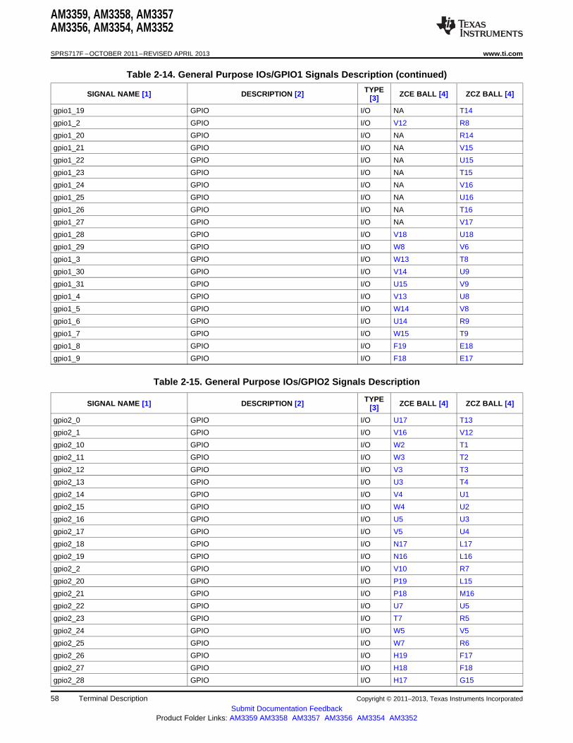
AM3359, AM3358, AM3357AM3356, AM3354, AM3352
SPRS717F –OCTOBER 2011–REVISED APRIL 2013 www.ti.com
Table 2-14. General Purpose IOs/GPIO1 Signals Description (continued)
TYPESIGNAL NAME [1] DESCRIPTION [2] ZCE BALL [4] ZCZ BALL [4][3]
gpio1_19 GPIO I/O NA T14
gpio1_2 GPIO I/O V12 R8
gpio1_20 GPIO I/O NA R14
gpio1_21 GPIO I/O NA V15
gpio1_22 GPIO I/O NA U15
gpio1_23 GPIO I/O NA T15
gpio1_24 GPIO I/O NA V16
gpio1_25 GPIO I/O NA U16
gpio1_26 GPIO I/O NA T16
gpio1_27 GPIO I/O NA V17
gpio1_28 GPIO I/O V18 U18
gpio1_29 GPIO I/O W8 V6
gpio1_3 GPIO I/O W13 T8
gpio1_30 GPIO I/O V14 U9
gpio1_31 GPIO I/O U15 V9
gpio1_4 GPIO I/O V13 U8
gpio1_5 GPIO I/O W14 V8
gpio1_6 GPIO I/O U14 R9
gpio1_7 GPIO I/O W15 T9
gpio1_8 GPIO I/O F19 E18
gpio1_9 GPIO I/O F18 E17
Table 2-15. General Purpose IOs/GPIO2 Signals Description
TYPESIGNAL NAME [1] DESCRIPTION [2] ZCE BALL [4] ZCZ BALL [4][3]
gpio2_0 GPIO I/O U17 T13
gpio2_1 GPIO I/O V16 V12
gpio2_10 GPIO I/O W2 T1
gpio2_11 GPIO I/O W3 T2
gpio2_12 GPIO I/O V3 T3
gpio2_13 GPIO I/O U3 T4
gpio2_14 GPIO I/O V4 U1
gpio2_15 GPIO I/O W4 U2
gpio2_16 GPIO I/O U5 U3
gpio2_17 GPIO I/O V5 U4
gpio2_18 GPIO I/O N17 L17
gpio2_19 GPIO I/O N16 L16
gpio2_2 GPIO I/O V10 R7
gpio2_20 GPIO I/O P19 L15
gpio2_21 GPIO I/O P18 M16
gpio2_22 GPIO I/O U7 U5
gpio2_23 GPIO I/O T7 R5
gpio2_24 GPIO I/O W5 V5
gpio2_25 GPIO I/O W7 R6
gpio2_26 GPIO I/O H19 F17
gpio2_27 GPIO I/O H18 F18
gpio2_28 GPIO I/O H17 G15
58 Terminal Description Copyright © 2011–2013, Texas Instruments Incorporated
Submit Documentation FeedbackProduct Folder Links: AM3359 AM3358 AM3357 AM3356 AM3354 AM3352

AM3359, AM3358, AM3357AM3356, AM3354, AM3352
www.ti.com SPRS717F –OCTOBER 2011–REVISED APRIL 2013
Table 2-15. General Purpose IOs/GPIO2 Signals Description (continued)
TYPESIGNAL NAME [1] DESCRIPTION [2] ZCE BALL [4] ZCZ BALL [4][3]
gpio2_29 GPIO I/O G18 G16
gpio2_3 GPIO I/O W9 T7
gpio2_30 GPIO I/O G19 G17
gpio2_31 GPIO I/O G17 G18
gpio2_4 GPIO I/O U8 U6
gpio2_5 GPIO I/O V8 T6
gpio2_6 GPIO I/O U1 R1
gpio2_7 GPIO I/O U2 R2
gpio2_8 GPIO I/O V1 R3
gpio2_9 GPIO I/O V2 R4
Table 2-16. General Purpose IOs/GPIO3 Signals Description
TYPESIGNAL NAME [1] DESCRIPTION [2] ZCE BALL [4] ZCZ BALL [4][3]
gpio3_0 GPIO I/O J19 H16
gpio3_1 GPIO I/O J18 H17
gpio3_10 GPIO I/O M19 L18
gpio3_13 GPIO I/O NA F15
gpio3_14 GPIO I/O NA A13
gpio3_15 GPIO I/O NA B13
gpio3_16 GPIO I/O NA D12
gpio3_17 GPIO I/O NA C12
gpio3_18 GPIO I/O NA B12
gpio3_19 GPIO I/O NA C13
gpio3_2 GPIO I/O K19 J15
gpio3_20 GPIO I/O NA D13
gpio3_21 GPIO I/O NA A14
gpio3_3 GPIO I/O K17 J16
gpio3_4 GPIO I/O L19 J17
gpio3_5 GPIO I/O C18 C17
gpio3_6 GPIO I/O B19 C16
gpio3_7 GPIO I/O A15 C14
gpio3_8 GPIO I/O D14 B14
gpio3_9 GPIO I/O N19 K18
Copyright © 2011–2013, Texas Instruments Incorporated Terminal Description 59Submit Documentation Feedback
Product Folder Links: AM3359 AM3358 AM3357 AM3356 AM3354 AM3352

AM3359, AM3358, AM3357AM3356, AM3354, AM3352
SPRS717F –OCTOBER 2011–REVISED APRIL 2013 www.ti.com
2.3.3 Miscellaneous
Table 2-17. Miscellaneous/Miscellaneous Signals Description
TYPESIGNAL NAME [1] DESCRIPTION [2] ZCE BALL [4] ZCZ BALL [4][3]
clkout1 Clock out1 O C15 A15
clkout2 Clock out2 O B15 D14
ENZ_KALDO_1P8V Active low enable input for internal I A7 B4CAP_VDD_RTC voltage regulator
EXT_WAKEUP EXT_WAKEUP input I B5 C5
nNMI External Interrupt to ARM Cortext A8 core I C17 B18
nRESETIN_OUT Active low Warm Reset I/OD A16 A10
OSC0_IN High frequency oscillator input I W11 V10
OSC0_OUT High frequency oscillator output O W12 U11
OSC1_IN Low frequency (32.768 KHz) Real Time Clock I A6 A6oscillator input
OSC1_OUT Low frequency (32.768 KHz) Real Time Clock O A5 A4oscillator output
PMIC_POWER_EN PMIC_POWER_EN output O C7 C6
porz Active low Power on Reset I E15 B15
RTC_PORz Active low RTC reset input I B7 B5
tclkin Timer Clock In I B15 D14
xdma_event_intr0 External DMA Event or Interrupt 0 I C15 A15
xdma_event_intr1 External DMA Event or Interrupt 1 I B15 D14
xdma_event_intr2 External DMA Event or Interrupt 2 I B16, E18, K18 C15, C18, H18
60 Terminal Description Copyright © 2011–2013, Texas Instruments Incorporated
Submit Documentation FeedbackProduct Folder Links: AM3359 AM3358 AM3357 AM3356 AM3354 AM3352
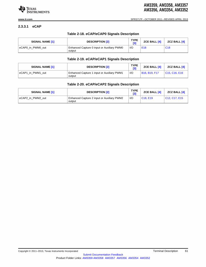
AM3359, AM3358, AM3357AM3356, AM3354, AM3352
www.ti.com SPRS717F –OCTOBER 2011–REVISED APRIL 2013
2.3.3.1 eCAP
Table 2-18. eCAP/eCAP0 Signals Description
TYPESIGNAL NAME [1] DESCRIPTION [2] ZCE BALL [4] ZCZ BALL [4][3]
eCAP0_in_PWM0_out Enhanced Capture 0 input or Auxiliary PWM0 I/O E18 C18output
Table 2-19. eCAP/eCAP1 Signals Description
TYPESIGNAL NAME [1] DESCRIPTION [2] ZCE BALL [4] ZCZ BALL [4][3]
eCAP1_in_PWM1_out Enhanced Capture 1 input or Auxiliary PWM1 I/O B16, B19, F17 C15, C16, E16output
Table 2-20. eCAP/eCAP2 Signals Description
TYPESIGNAL NAME [1] DESCRIPTION [2] ZCE BALL [4] ZCZ BALL [4][3]
eCAP2_in_PWM2_out Enhanced Capture 2 input or Auxiliary PWM2 I/O C18, E19 C12, C17, E15output
Copyright © 2011–2013, Texas Instruments Incorporated Terminal Description 61Submit Documentation Feedback
Product Folder Links: AM3359 AM3358 AM3357 AM3356 AM3354 AM3352

AM3359, AM3358, AM3357AM3356, AM3354, AM3352
SPRS717F –OCTOBER 2011–REVISED APRIL 2013 www.ti.com
2.3.3.2 eHRPWM
Table 2-21. eHRPWM/eHRPWM0 Signals Description
TYPESIGNAL NAME [1] DESCRIPTION [2] ZCE BALL [4] ZCZ BALL [4][3]
ehrpwm0A eHRPWM0 A output. O A18 A13, A17
ehrpwm0B eHRPWM0 B output. O B18 B13, B17
ehrpwm0_synci Sync input to eHRPWM0 module from an I A17 A16, C12external pin
ehrpwm0_synco Sync Output from eHRPWM0 module to an O U12, V2, W4 R4, U12, U2, V14external pin
ehrpwm0_tripzone_input eHRPWM0 trip zone input I B17 B16, D12
Table 2-22. eHRPWM/eHRPWM1 Signals Description
TYPESIGNAL NAME [1] DESCRIPTION [2] ZCE BALL [4] ZCZ BALL [4][3]
ehrpwm1A eHRPWM1 A output. O U5 U14, U3
ehrpwm1B eHRPWM1 B output. O V5 T14, U4
ehrpwm1_tripzone_input eHRPWM1 trip zone input I V4 R13, U1
Table 2-23. eHRPWM/eHRPWM2 Signals Description
TYPESIGNAL NAME [1] DESCRIPTION [2] ZCE BALL [4] ZCZ BALL [4][3]
ehrpwm2A eHRPWM2 A output. O U1, V15 R1, U10
ehrpwm2B eHRPWM2 B output. O U2, W16 R2, T10
ehrpwm2_tripzone_input eHRPWM2 trip zone input I T12, V1 R3, T11
62 Terminal Description Copyright © 2011–2013, Texas Instruments Incorporated
Submit Documentation FeedbackProduct Folder Links: AM3359 AM3358 AM3357 AM3356 AM3354 AM3352

AM3359, AM3358, AM3357AM3356, AM3354, AM3352
www.ti.com SPRS717F –OCTOBER 2011–REVISED APRIL 2013
2.3.3.3 eQEP
Table 2-24. eQEP/eQEP0 Signals Description
TYPESIGNAL NAME [1] DESCRIPTION [2] ZCE BALL [4] ZCZ BALL [4][3]
eQEP0A_in eQEP0A quadrature input I M18 B12, K16
eQEP0B_in eQEP0B quadrature input I L18 C13, K17
eQEP0_index eQEP0 index. I/O K17 D13, J16
eQEP0_strobe eQEP0 strobe. I/O P19 A14, L15
Table 2-25. eQEP/eQEP1 Signals Description
TYPESIGNAL NAME [1] DESCRIPTION [2] ZCE BALL [4] ZCZ BALL [4][3]
eQEP1A_in eQEP1A quadrature input I V6 R14, V2
eQEP1B_in eQEP1B quadrature input I U6 V15, V3
eQEP1_index eQEP1 index. I/O W6 U15, V4
eQEP1_strobe eQEP1 strobe. I/O V7 T15, T5
Table 2-26. eQEP/eQEP2 Signals Description
TYPESIGNAL NAME [1] DESCRIPTION [2] ZCE BALL [4] ZCZ BALL [4][3]
eQEP2A_in eQEP2A quadrature input I U13, W2 T1, T12
eQEP2B_in eQEP2B quadrature input I T13, W3 R12, T2
eQEP2_index eQEP2 index. I/O V3, W17 T3, V13
eQEP2_strobe eQEP2 strobe. I/O U3, V17 T4, U13
Copyright © 2011–2013, Texas Instruments Incorporated Terminal Description 63Submit Documentation Feedback
Product Folder Links: AM3359 AM3358 AM3357 AM3356 AM3354 AM3352
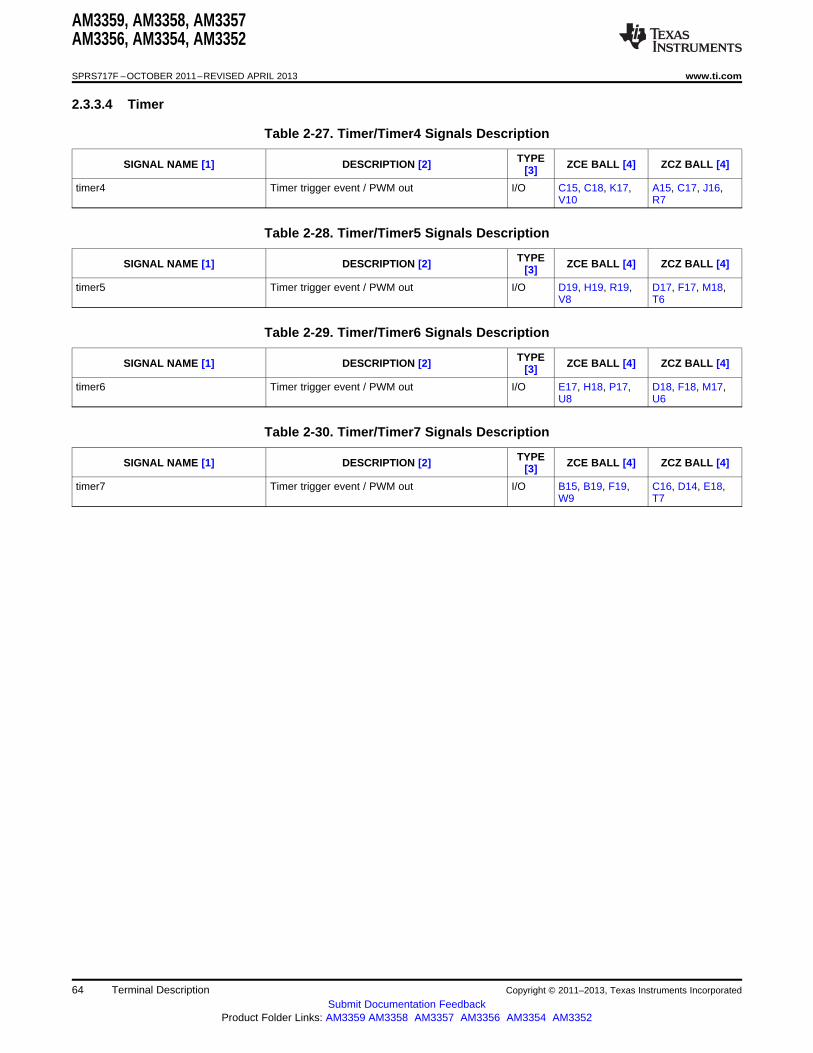
AM3359, AM3358, AM3357AM3356, AM3354, AM3352
SPRS717F –OCTOBER 2011–REVISED APRIL 2013 www.ti.com
2.3.3.4 Timer
Table 2-27. Timer/Timer4 Signals Description
TYPESIGNAL NAME [1] DESCRIPTION [2] ZCE BALL [4] ZCZ BALL [4][3]
timer4 Timer trigger event / PWM out I/O C15, C18, K17, A15, C17, J16,V10 R7
Table 2-28. Timer/Timer5 Signals Description
TYPESIGNAL NAME [1] DESCRIPTION [2] ZCE BALL [4] ZCZ BALL [4][3]
timer5 Timer trigger event / PWM out I/O D19, H19, R19, D17, F17, M18,V8 T6
Table 2-29. Timer/Timer6 Signals Description
TYPESIGNAL NAME [1] DESCRIPTION [2] ZCE BALL [4] ZCZ BALL [4][3]
timer6 Timer trigger event / PWM out I/O E17, H18, P17, D18, F18, M17,U8 U6
Table 2-30. Timer/Timer7 Signals Description
TYPESIGNAL NAME [1] DESCRIPTION [2] ZCE BALL [4] ZCZ BALL [4][3]
timer7 Timer trigger event / PWM out I/O B15, B19, F19, C16, D14, E18,W9 T7
64 Terminal Description Copyright © 2011–2013, Texas Instruments Incorporated
Submit Documentation FeedbackProduct Folder Links: AM3359 AM3358 AM3357 AM3356 AM3354 AM3352
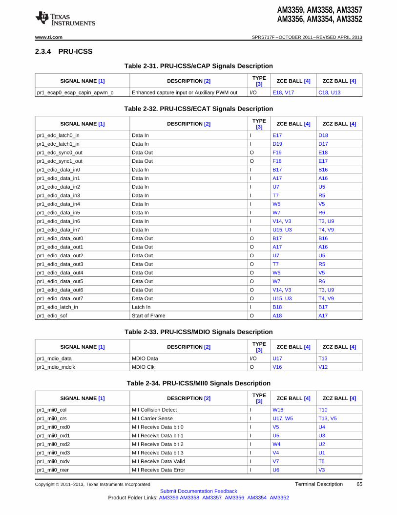
AM3359, AM3358, AM3357AM3356, AM3354, AM3352
www.ti.com SPRS717F –OCTOBER 2011–REVISED APRIL 2013
2.3.4 PRU-ICSS
Table 2-31. PRU-ICSS/eCAP Signals Description
TYPESIGNAL NAME [1] DESCRIPTION [2] ZCE BALL [4] ZCZ BALL [4][3]
pr1_ecap0_ecap_capin_apwm_o Enhanced capture input or Auxiliary PWM out I/O E18, V17 C18, U13
Table 2-32. PRU-ICSS/ECAT Signals Description
TYPESIGNAL NAME [1] DESCRIPTION [2] ZCE BALL [4] ZCZ BALL [4][3]
pr1_edc_latch0_in Data In I E17 D18
pr1_edc_latch1_in Data In I D19 D17
pr1_edc_sync0_out Data Out O F19 E18
pr1_edc_sync1_out Data Out O F18 E17
pr1_edio_data_in0 Data In I B17 B16
pr1_edio_data_in1 Data In I A17 A16
pr1_edio_data_in2 Data In I U7 U5
pr1_edio_data_in3 Data In I T7 R5
pr1_edio_data_in4 Data In I W5 V5
pr1_edio_data_in5 Data In I W7 R6
pr1_edio_data_in6 Data In I V14, V3 T3, U9
pr1_edio_data_in7 Data In I U15, U3 T4, V9
pr1_edio_data_out0 Data Out O B17 B16
pr1_edio_data_out1 Data Out O A17 A16
pr1_edio_data_out2 Data Out O U7 U5
pr1_edio_data_out3 Data Out O T7 R5
pr1_edio_data_out4 Data Out O W5 V5
pr1_edio_data_out5 Data Out O W7 R6
pr1_edio_data_out6 Data Out O V14, V3 T3, U9
pr1_edio_data_out7 Data Out O U15, U3 T4, V9
pr1_edio_latch_in Latch In I B18 B17
pr1_edio_sof Start of Frame O A18 A17
Table 2-33. PRU-ICSS/MDIO Signals Description
TYPESIGNAL NAME [1] DESCRIPTION [2] ZCE BALL [4] ZCZ BALL [4][3]
pr1_mdio_data MDIO Data I/O U17 T13
pr1_mdio_mdclk MDIO Clk O V16 V12
Table 2-34. PRU-ICSS/MII0 Signals Description
TYPESIGNAL NAME [1] DESCRIPTION [2] ZCE BALL [4] ZCZ BALL [4][3]
pr1_mii0_col MII Collision Detect I W16 T10
pr1_mii0_crs MII Carrier Sense I U17, W5 T13, V5
pr1_mii0_rxd0 MII Receive Data bit 0 I V5 U4
pr1_mii0_rxd1 MII Receive Data bit 1 I U5 U3
pr1_mii0_rxd2 MII Receive Data bit 2 I W4 U2
pr1_mii0_rxd3 MII Receive Data bit 3 I V4 U1
pr1_mii0_rxdv MII Receive Data Valid I V7 T5
pr1_mii0_rxer MII Receive Data Error I U6 V3
Copyright © 2011–2013, Texas Instruments Incorporated Terminal Description 65Submit Documentation Feedback
Product Folder Links: AM3359 AM3358 AM3357 AM3356 AM3354 AM3352
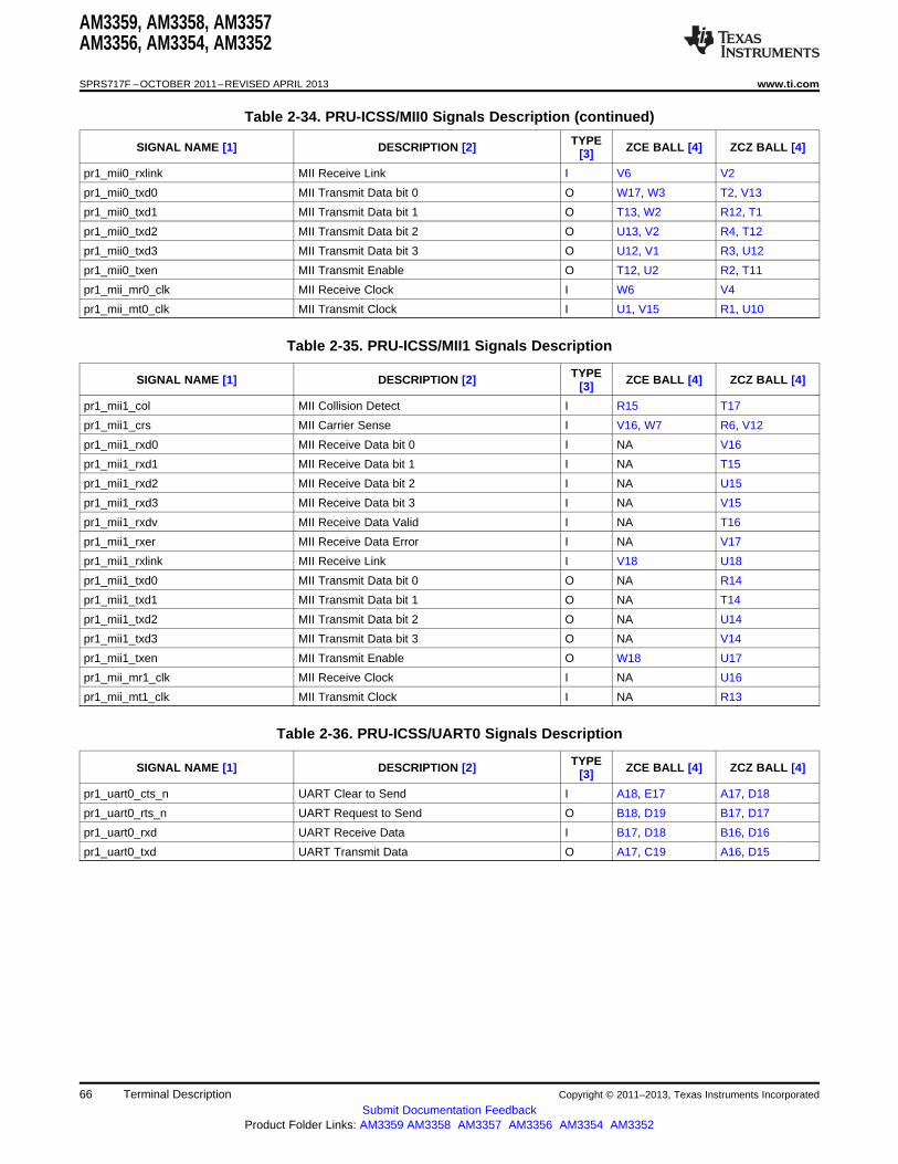
AM3359, AM3358, AM3357AM3356, AM3354, AM3352
SPRS717F –OCTOBER 2011–REVISED APRIL 2013 www.ti.com
Table 2-34. PRU-ICSS/MII0 Signals Description (continued)
TYPESIGNAL NAME [1] DESCRIPTION [2] ZCE BALL [4] ZCZ BALL [4][3]
pr1_mii0_rxlink MII Receive Link I V6 V2
pr1_mii0_txd0 MII Transmit Data bit 0 O W17, W3 T2, V13
pr1_mii0_txd1 MII Transmit Data bit 1 O T13, W2 R12, T1
pr1_mii0_txd2 MII Transmit Data bit 2 O U13, V2 R4, T12
pr1_mii0_txd3 MII Transmit Data bit 3 O U12, V1 R3, U12
pr1_mii0_txen MII Transmit Enable O T12, U2 R2, T11
pr1_mii_mr0_clk MII Receive Clock I W6 V4
pr1_mii_mt0_clk MII Transmit Clock I U1, V15 R1, U10
Table 2-35. PRU-ICSS/MII1 Signals Description
TYPESIGNAL NAME [1] DESCRIPTION [2] ZCE BALL [4] ZCZ BALL [4][3]
pr1_mii1_col MII Collision Detect I R15 T17
pr1_mii1_crs MII Carrier Sense I V16, W7 R6, V12
pr1_mii1_rxd0 MII Receive Data bit 0 I NA V16
pr1_mii1_rxd1 MII Receive Data bit 1 I NA T15
pr1_mii1_rxd2 MII Receive Data bit 2 I NA U15
pr1_mii1_rxd3 MII Receive Data bit 3 I NA V15
pr1_mii1_rxdv MII Receive Data Valid I NA T16
pr1_mii1_rxer MII Receive Data Error I NA V17
pr1_mii1_rxlink MII Receive Link I V18 U18
pr1_mii1_txd0 MII Transmit Data bit 0 O NA R14
pr1_mii1_txd1 MII Transmit Data bit 1 O NA T14
pr1_mii1_txd2 MII Transmit Data bit 2 O NA U14
pr1_mii1_txd3 MII Transmit Data bit 3 O NA V14
pr1_mii1_txen MII Transmit Enable O W18 U17
pr1_mii_mr1_clk MII Receive Clock I NA U16
pr1_mii_mt1_clk MII Transmit Clock I NA R13
Table 2-36. PRU-ICSS/UART0 Signals Description
TYPESIGNAL NAME [1] DESCRIPTION [2] ZCE BALL [4] ZCZ BALL [4][3]
pr1_uart0_cts_n UART Clear to Send I A18, E17 A17, D18
pr1_uart0_rts_n UART Request to Send O B18, D19 B17, D17
pr1_uart0_rxd UART Receive Data I B17, D18 B16, D16
pr1_uart0_txd UART Transmit Data O A17, C19 A16, D15
66 Terminal Description Copyright © 2011–2013, Texas Instruments Incorporated
Submit Documentation FeedbackProduct Folder Links: AM3359 AM3358 AM3357 AM3356 AM3354 AM3352
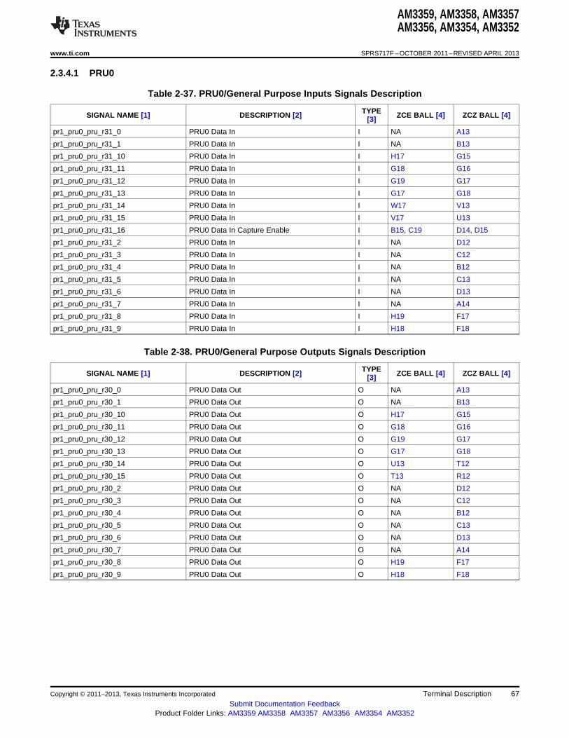
AM3359, AM3358, AM3357AM3356, AM3354, AM3352
www.ti.com SPRS717F –OCTOBER 2011–REVISED APRIL 2013
2.3.4.1 PRU0
Table 2-37. PRU0/General Purpose Inputs Signals Description
TYPESIGNAL NAME [1] DESCRIPTION [2] ZCE BALL [4] ZCZ BALL [4][3]
pr1_pru0_pru_r31_0 PRU0 Data In I NA A13
pr1_pru0_pru_r31_1 PRU0 Data In I NA B13
pr1_pru0_pru_r31_10 PRU0 Data In I H17 G15
pr1_pru0_pru_r31_11 PRU0 Data In I G18 G16
pr1_pru0_pru_r31_12 PRU0 Data In I G19 G17
pr1_pru0_pru_r31_13 PRU0 Data In I G17 G18
pr1_pru0_pru_r31_14 PRU0 Data In I W17 V13
pr1_pru0_pru_r31_15 PRU0 Data In I V17 U13
pr1_pru0_pru_r31_16 PRU0 Data In Capture Enable I B15, C19 D14, D15
pr1_pru0_pru_r31_2 PRU0 Data In I NA D12
pr1_pru0_pru_r31_3 PRU0 Data In I NA C12
pr1_pru0_pru_r31_4 PRU0 Data In I NA B12
pr1_pru0_pru_r31_5 PRU0 Data In I NA C13
pr1_pru0_pru_r31_6 PRU0 Data In I NA D13
pr1_pru0_pru_r31_7 PRU0 Data In I NA A14
pr1_pru0_pru_r31_8 PRU0 Data In I H19 F17
pr1_pru0_pru_r31_9 PRU0 Data In I H18 F18
Table 2-38. PRU0/General Purpose Outputs Signals Description
TYPESIGNAL NAME [1] DESCRIPTION [2] ZCE BALL [4] ZCZ BALL [4][3]
pr1_pru0_pru_r30_0 PRU0 Data Out O NA A13
pr1_pru0_pru_r30_1 PRU0 Data Out O NA B13
pr1_pru0_pru_r30_10 PRU0 Data Out O H17 G15
pr1_pru0_pru_r30_11 PRU0 Data Out O G18 G16
pr1_pru0_pru_r30_12 PRU0 Data Out O G19 G17
pr1_pru0_pru_r30_13 PRU0 Data Out O G17 G18
pr1_pru0_pru_r30_14 PRU0 Data Out O U13 T12
pr1_pru0_pru_r30_15 PRU0 Data Out O T13 R12
pr1_pru0_pru_r30_2 PRU0 Data Out O NA D12
pr1_pru0_pru_r30_3 PRU0 Data Out O NA C12
pr1_pru0_pru_r30_4 PRU0 Data Out O NA B12
pr1_pru0_pru_r30_5 PRU0 Data Out O NA C13
pr1_pru0_pru_r30_6 PRU0 Data Out O NA D13
pr1_pru0_pru_r30_7 PRU0 Data Out O NA A14
pr1_pru0_pru_r30_8 PRU0 Data Out O H19 F17
pr1_pru0_pru_r30_9 PRU0 Data Out O H18 F18
Copyright © 2011–2013, Texas Instruments Incorporated Terminal Description 67Submit Documentation Feedback
Product Folder Links: AM3359 AM3358 AM3357 AM3356 AM3354 AM3352
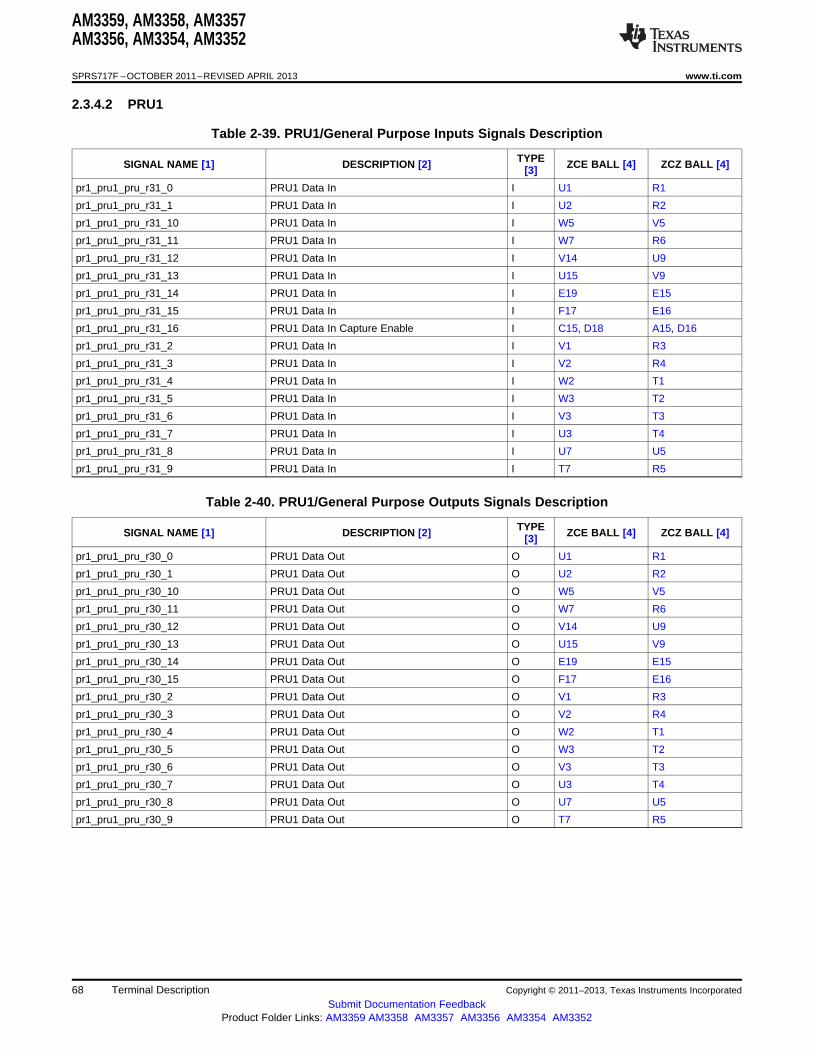
AM3359, AM3358, AM3357AM3356, AM3354, AM3352
SPRS717F –OCTOBER 2011–REVISED APRIL 2013 www.ti.com
2.3.4.2 PRU1
Table 2-39. PRU1/General Purpose Inputs Signals Description
TYPESIGNAL NAME [1] DESCRIPTION [2] ZCE BALL [4] ZCZ BALL [4][3]
pr1_pru1_pru_r31_0 PRU1 Data In I U1 R1
pr1_pru1_pru_r31_1 PRU1 Data In I U2 R2
pr1_pru1_pru_r31_10 PRU1 Data In I W5 V5
pr1_pru1_pru_r31_11 PRU1 Data In I W7 R6
pr1_pru1_pru_r31_12 PRU1 Data In I V14 U9
pr1_pru1_pru_r31_13 PRU1 Data In I U15 V9
pr1_pru1_pru_r31_14 PRU1 Data In I E19 E15
pr1_pru1_pru_r31_15 PRU1 Data In I F17 E16
pr1_pru1_pru_r31_16 PRU1 Data In Capture Enable I C15, D18 A15, D16
pr1_pru1_pru_r31_2 PRU1 Data In I V1 R3
pr1_pru1_pru_r31_3 PRU1 Data In I V2 R4
pr1_pru1_pru_r31_4 PRU1 Data In I W2 T1
pr1_pru1_pru_r31_5 PRU1 Data In I W3 T2
pr1_pru1_pru_r31_6 PRU1 Data In I V3 T3
pr1_pru1_pru_r31_7 PRU1 Data In I U3 T4
pr1_pru1_pru_r31_8 PRU1 Data In I U7 U5
pr1_pru1_pru_r31_9 PRU1 Data In I T7 R5
Table 2-40. PRU1/General Purpose Outputs Signals Description
TYPESIGNAL NAME [1] DESCRIPTION [2] ZCE BALL [4] ZCZ BALL [4][3]
pr1_pru1_pru_r30_0 PRU1 Data Out O U1 R1
pr1_pru1_pru_r30_1 PRU1 Data Out O U2 R2
pr1_pru1_pru_r30_10 PRU1 Data Out O W5 V5
pr1_pru1_pru_r30_11 PRU1 Data Out O W7 R6
pr1_pru1_pru_r30_12 PRU1 Data Out O V14 U9
pr1_pru1_pru_r30_13 PRU1 Data Out O U15 V9
pr1_pru1_pru_r30_14 PRU1 Data Out O E19 E15
pr1_pru1_pru_r30_15 PRU1 Data Out O F17 E16
pr1_pru1_pru_r30_2 PRU1 Data Out O V1 R3
pr1_pru1_pru_r30_3 PRU1 Data Out O V2 R4
pr1_pru1_pru_r30_4 PRU1 Data Out O W2 T1
pr1_pru1_pru_r30_5 PRU1 Data Out O W3 T2
pr1_pru1_pru_r30_6 PRU1 Data Out O V3 T3
pr1_pru1_pru_r30_7 PRU1 Data Out O U3 T4
pr1_pru1_pru_r30_8 PRU1 Data Out O U7 U5
pr1_pru1_pru_r30_9 PRU1 Data Out O T7 R5
68 Terminal Description Copyright © 2011–2013, Texas Instruments Incorporated
Submit Documentation FeedbackProduct Folder Links: AM3359 AM3358 AM3357 AM3356 AM3354 AM3352
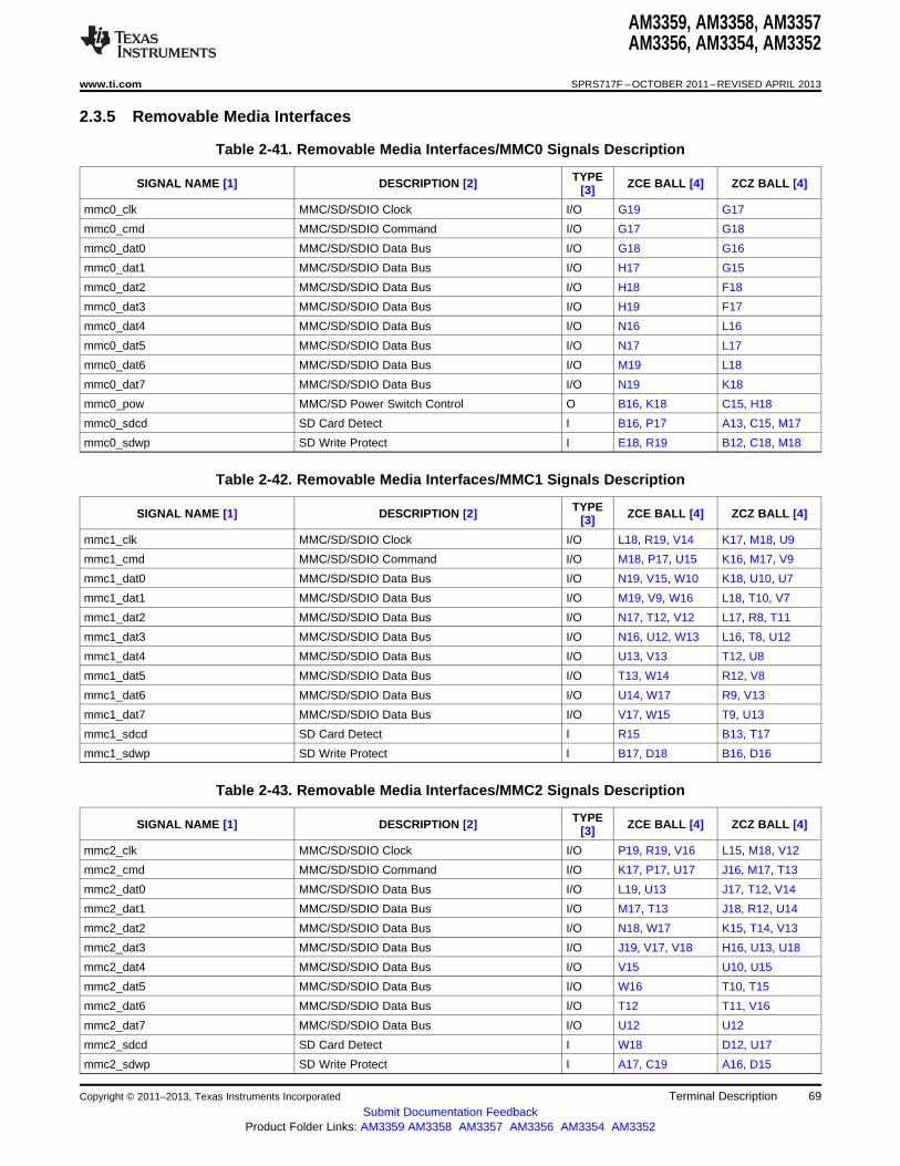
AM3359, AM3358, AM3357AM3356, AM3354, AM3352
www.ti.com SPRS717F –OCTOBER 2011–REVISED APRIL 2013
2.3.5 Removable Media Interfaces
Table 2-41. Removable Media Interfaces/MMC0 Signals Description
TYPESIGNAL NAME [1] DESCRIPTION [2] ZCE BALL [4] ZCZ BALL [4][3]
mmc0_clk MMC/SD/SDIO Clock I/O G19 G17
mmc0_cmd MMC/SD/SDIO Command I/O G17 G18
mmc0_dat0 MMC/SD/SDIO Data Bus I/O G18 G16
mmc0_dat1 MMC/SD/SDIO Data Bus I/O H17 G15
mmc0_dat2 MMC/SD/SDIO Data Bus I/O H18 F18
mmc0_dat3 MMC/SD/SDIO Data Bus I/O H19 F17
mmc0_dat4 MMC/SD/SDIO Data Bus I/O N16 L16
mmc0_dat5 MMC/SD/SDIO Data Bus I/O N17 L17
mmc0_dat6 MMC/SD/SDIO Data Bus I/O M19 L18
mmc0_dat7 MMC/SD/SDIO Data Bus I/O N19 K18
mmc0_pow MMC/SD Power Switch Control O B16, K18 C15, H18
mmc0_sdcd SD Card Detect I B16, P17 A13, C15, M17
mmc0_sdwp SD Write Protect I E18, R19 B12, C18, M18
Table 2-42. Removable Media Interfaces/MMC1 Signals Description
TYPESIGNAL NAME [1] DESCRIPTION [2] ZCE BALL [4] ZCZ BALL [4][3]
mmc1_clk MMC/SD/SDIO Clock I/O L18, R19, V14 K17, M18, U9
mmc1_cmd MMC/SD/SDIO Command I/O M18, P17, U15 K16, M17, V9
mmc1_dat0 MMC/SD/SDIO Data Bus I/O N19, V15, W10 K18, U10, U7
mmc1_dat1 MMC/SD/SDIO Data Bus I/O M19, V9, W16 L18, T10, V7
mmc1_dat2 MMC/SD/SDIO Data Bus I/O N17, T12, V12 L17, R8, T11
mmc1_dat3 MMC/SD/SDIO Data Bus I/O N16, U12, W13 L16, T8, U12
mmc1_dat4 MMC/SD/SDIO Data Bus I/O U13, V13 T12, U8
mmc1_dat5 MMC/SD/SDIO Data Bus I/O T13, W14 R12, V8
mmc1_dat6 MMC/SD/SDIO Data Bus I/O U14, W17 R9, V13
mmc1_dat7 MMC/SD/SDIO Data Bus I/O V17, W15 T9, U13
mmc1_sdcd SD Card Detect I R15 B13, T17
mmc1_sdwp SD Write Protect I B17, D18 B16, D16
Table 2-43. Removable Media Interfaces/MMC2 Signals Description
TYPESIGNAL NAME [1] DESCRIPTION [2] ZCE BALL [4] ZCZ BALL [4][3]
mmc2_clk MMC/SD/SDIO Clock I/O P19, R19, V16 L15, M18, V12
mmc2_cmd MMC/SD/SDIO Command I/O K17, P17, U17 J16, M17, T13
mmc2_dat0 MMC/SD/SDIO Data Bus I/O L19, U13 J17, T12, V14
mmc2_dat1 MMC/SD/SDIO Data Bus I/O M17, T13 J18, R12, U14
mmc2_dat2 MMC/SD/SDIO Data Bus I/O N18, W17 K15, T14, V13
mmc2_dat3 MMC/SD/SDIO Data Bus I/O J19, V17, V18 H16, U13, U18
mmc2_dat4 MMC/SD/SDIO Data Bus I/O V15 U10, U15
mmc2_dat5 MMC/SD/SDIO Data Bus I/O W16 T10, T15
mmc2_dat6 MMC/SD/SDIO Data Bus I/O T12 T11, V16
mmc2_dat7 MMC/SD/SDIO Data Bus I/O U12 U12
mmc2_sdcd SD Card Detect I W18 D12, U17
mmc2_sdwp SD Write Protect I A17, C19 A16, D15
Copyright © 2011–2013, Texas Instruments Incorporated Terminal Description 69Submit Documentation Feedback
Product Folder Links: AM3359 AM3358 AM3357 AM3356 AM3354 AM3352
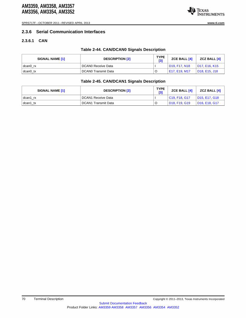
AM3359, AM3358, AM3357AM3356, AM3354, AM3352
SPRS717F –OCTOBER 2011–REVISED APRIL 2013 www.ti.com
2.3.6 Serial Communication Interfaces
2.3.6.1 CAN
Table 2-44. CAN/DCAN0 Signals Description
TYPESIGNAL NAME [1] DESCRIPTION [2] ZCE BALL [4] ZCZ BALL [4][3]
dcan0_rx DCAN0 Receive Data I D19, F17, N18 D17, E16, K15
dcan0_tx DCAN0 Transmit Data O E17, E19, M17 D18, E15, J18
Table 2-45. CAN/DCAN1 Signals Description
TYPESIGNAL NAME [1] DESCRIPTION [2] ZCE BALL [4] ZCZ BALL [4][3]
dcan1_rx DCAN1 Receive Data I C19, F18, G17 D15, E17, G18
dcan1_tx DCAN1 Transmit Data O D18, F19, G19 D16, E18, G17
70 Terminal Description Copyright © 2011–2013, Texas Instruments Incorporated
Submit Documentation FeedbackProduct Folder Links: AM3359 AM3358 AM3357 AM3356 AM3354 AM3352
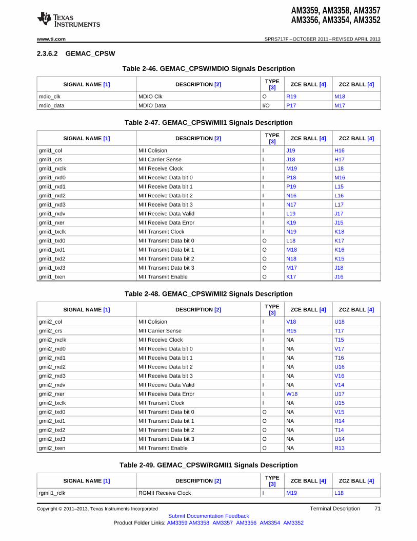
AM3359, AM3358, AM3357AM3356, AM3354, AM3352
www.ti.com SPRS717F –OCTOBER 2011–REVISED APRIL 2013
2.3.6.2 GEMAC_CPSW
Table 2-46. GEMAC_CPSW/MDIO Signals Description
TYPESIGNAL NAME [1] DESCRIPTION [2] ZCE BALL [4] ZCZ BALL [4][3]
mdio_clk MDIO Clk O R19 M18
mdio_data MDIO Data I/O P17 M17
Table 2-47. GEMAC_CPSW/MII1 Signals Description
TYPESIGNAL NAME [1] DESCRIPTION [2] ZCE BALL [4] ZCZ BALL [4][3]
gmii1_col MII Colision I J19 H16
gmii1_crs MII Carrier Sense I J18 H17
gmii1_rxclk MII Receive Clock I M19 L18
gmii1_rxd0 MII Receive Data bit 0 I P18 M16
gmii1_rxd1 MII Receive Data bit 1 I P19 L15
gmii1_rxd2 MII Receive Data bit 2 I N16 L16
gmii1_rxd3 MII Receive Data bit 3 I N17 L17
gmii1_rxdv MII Receive Data Valid I L19 J17
gmii1_rxer MII Receive Data Error I K19 J15
gmii1_txclk MII Transmit Clock I N19 K18
gmii1_txd0 MII Transmit Data bit 0 O L18 K17
gmii1_txd1 MII Transmit Data bit 1 O M18 K16
gmii1_txd2 MII Transmit Data bit 2 O N18 K15
gmii1_txd3 MII Transmit Data bit 3 O M17 J18
gmii1_txen MII Transmit Enable O K17 J16
Table 2-48. GEMAC_CPSW/MII2 Signals Description
TYPESIGNAL NAME [1] DESCRIPTION [2] ZCE BALL [4] ZCZ BALL [4][3]
gmii2_col MII Colision I V18 U18
gmii2_crs MII Carrier Sense I R15 T17
gmii2_rxclk MII Receive Clock I NA T15
gmii2_rxd0 MII Receive Data bit 0 I NA V17
gmii2_rxd1 MII Receive Data bit 1 I NA T16
gmii2_rxd2 MII Receive Data bit 2 I NA U16
gmii2_rxd3 MII Receive Data bit 3 I NA V16
gmii2_rxdv MII Receive Data Valid I NA V14
gmii2_rxer MII Receive Data Error I W18 U17
gmii2_txclk MII Transmit Clock I NA U15
gmii2_txd0 MII Transmit Data bit 0 O NA V15
gmii2_txd1 MII Transmit Data bit 1 O NA R14
gmii2_txd2 MII Transmit Data bit 2 O NA T14
gmii2_txd3 MII Transmit Data bit 3 O NA U14
gmii2_txen MII Transmit Enable O NA R13
Table 2-49. GEMAC_CPSW/RGMII1 Signals Description
TYPESIGNAL NAME [1] DESCRIPTION [2] ZCE BALL [4] ZCZ BALL [4][3]
rgmii1_rclk RGMII Receive Clock I M19 L18
Copyright © 2011–2013, Texas Instruments Incorporated Terminal Description 71Submit Documentation Feedback
Product Folder Links: AM3359 AM3358 AM3357 AM3356 AM3354 AM3352
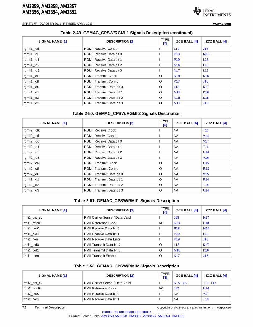
AM3359, AM3358, AM3357AM3356, AM3354, AM3352
SPRS717F –OCTOBER 2011–REVISED APRIL 2013 www.ti.com
Table 2-49. GEMAC_CPSW/RGMII1 Signals Description (continued)
TYPESIGNAL NAME [1] DESCRIPTION [2] ZCE BALL [4] ZCZ BALL [4][3]
rgmii1_rctl RGMII Receive Control I L19 J17
rgmii1_rd0 RGMII Receive Data bit 0 I P18 M16
rgmii1_rd1 RGMII Receive Data bit 1 I P19 L15
rgmii1_rd2 RGMII Receive Data bit 2 I N16 L16
rgmii1_rd3 RGMII Receive Data bit 3 I N17 L17
rgmii1_tclk RGMII Transmit Clock O N19 K18
rgmii1_tctl RGMII Transmit Control O K17 J16
rgmii1_td0 RGMII Transmit Data bit 0 O L18 K17
rgmii1_td1 RGMII Transmit Data bit 1 O M18 K16
rgmii1_td2 RGMII Transmit Data bit 2 O N18 K15
rgmii1_td3 RGMII Transmit Data bit 3 O M17 J18
Table 2-50. GEMAC_CPSW/RGMII2 Signals Description
TYPESIGNAL NAME [1] DESCRIPTION [2] ZCE BALL [4] ZCZ BALL [4][3]
rgmii2_rclk RGMII Receive Clock I NA T15
rgmii2_rctl RGMII Receive Control I NA V14
rgmii2_rd0 RGMII Receive Data bit 0 I NA V17
rgmii2_rd1 RGMII Receive Data bit 1 I NA T16
rgmii2_rd2 RGMII Receive Data bit 2 I NA U16
rgmii2_rd3 RGMII Receive Data bit 3 I NA V16
rgmii2_tclk RGMII Transmit Clock O NA U15
rgmii2_tctl RGMII Transmit Control O NA R13
rgmii2_td0 RGMII Transmit Data bit 0 O NA V15
rgmii2_td1 RGMII Transmit Data bit 1 O NA R14
rgmii2_td2 RGMII Transmit Data bit 2 O NA T14
rgmii2_td3 RGMII Transmit Data bit 3 O NA U14
Table 2-51. GEMAC_CPSW/RMII1 Signals Description
TYPESIGNAL NAME [1] DESCRIPTION [2] ZCE BALL [4] ZCZ BALL [4][3]
rmii1_crs_dv RMII Carrier Sense / Data Valid I J18 H17
rmii1_refclk RMII Reference Clock I/O K18 H18
rmii1_rxd0 RMII Receive Data bit 0 I P18 M16
rmii1_rxd1 RMII Receive Data bit 1 I P19 L15
rmii1_rxer RMII Receive Data Error I K19 J15
rmii1_txd0 RMII Transmit Data bit 0 O L18 K17
rmii1_txd1 RMII Transmit Data bit 1 O M18 K16
rmii1_txen RMII Transmit Enable O K17 J16
Table 2-52. GEMAC_CPSW/RMII2 Signals Description
TYPESIGNAL NAME [1] DESCRIPTION [2] ZCE BALL [4] ZCZ BALL [4][3]
rmii2_crs_dv RMII Carrier Sense / Data Valid I R15, U17 T13, T17
rmii2_refclk RMII Reference Clock I/O J19 H16
rmii2_rxd0 RMII Receive Data bit 0 I NA V17
rmii2_rxd1 RMII Receive Data bit 1 I NA T16
72 Terminal Description Copyright © 2011–2013, Texas Instruments Incorporated
Submit Documentation FeedbackProduct Folder Links: AM3359 AM3358 AM3357 AM3356 AM3354 AM3352
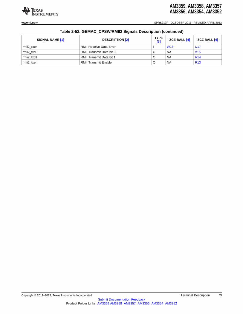
AM3359, AM3358, AM3357AM3356, AM3354, AM3352
www.ti.com SPRS717F –OCTOBER 2011–REVISED APRIL 2013
Table 2-52. GEMAC_CPSW/RMII2 Signals Description (continued)
TYPESIGNAL NAME [1] DESCRIPTION [2] ZCE BALL [4] ZCZ BALL [4][3]
rmii2_rxer RMII Receive Data Error I W18 U17
rmii2_txd0 RMII Transmit Data bit 0 O NA V15
rmii2_txd1 RMII Transmit Data bit 1 O NA R14
rmii2_txen RMII Transmit Enable O NA R13
Copyright © 2011–2013, Texas Instruments Incorporated Terminal Description 73Submit Documentation Feedback
Product Folder Links: AM3359 AM3358 AM3357 AM3356 AM3354 AM3352

AM3359, AM3358, AM3357AM3356, AM3354, AM3352
SPRS717F –OCTOBER 2011–REVISED APRIL 2013 www.ti.com
2.3.6.3 I2C
Table 2-53. I2C/I2C0 Signals Description
TYPESIGNAL NAME [1] DESCRIPTION [2] ZCE BALL [4] ZCZ BALL [4][3]
I2C0_SCL I2C0 Clock I/OD B19 C16
I2C0_SDA I2C0 Data I/OD C18 C17
Table 2-54. I2C/I2C1 Signals Description
TYPESIGNAL NAME [1] DESCRIPTION [2] ZCE BALL [4] ZCZ BALL [4][3]
I2C1_SCL I2C1 Clock I/OD A17, C19, F18, A16, D15, E17,K19 J15
I2C1_SDA I2C1 Data I/OD B17, D18, F19, B16, D16, E18,J18 H17
Table 2-55. I2C/I2C2 Signals Description
TYPESIGNAL NAME [1] DESCRIPTION [2] ZCE BALL [4] ZCZ BALL [4][3]
I2C2_SCL I2C2 Clock I/OD B18, D19, F17 B17, D17, E16
I2C2_SDA I2C2 Data I/OD A18, E17, E19 A17, D18, E15
74 Terminal Description Copyright © 2011–2013, Texas Instruments Incorporated
Submit Documentation FeedbackProduct Folder Links: AM3359 AM3358 AM3357 AM3356 AM3354 AM3352

AM3359, AM3358, AM3357AM3356, AM3354, AM3352
www.ti.com SPRS717F –OCTOBER 2011–REVISED APRIL 2013
2.3.6.4 McASP
Table 2-56. McASP/MCASP0 Signals Description
TYPESIGNAL NAME [1] DESCRIPTION [2] ZCE BALL [4] ZCZ BALL [4][3]
mcasp0_aclkr McASP0 Receive Bit Clock I/O L19, V18, V6 B12, J17, U18,V2
mcasp0_aclkx McASP0 Transmit Bit Clock I/O N19, V4 A13, K18, U1,V16
mcasp0_ahclkr McASP0 Receive Master Clock I/O V5 C12, U4
mcasp0_ahclkx McASP0 Transmit Master Clock I/O N18, V7 A14, K15, T5
mcasp0_axr0 McASP0 Serial Data (IN/OUT) I/O N17, U5 D12, L17, T16,U3
mcasp0_axr1 McASP0 Serial Data (IN/OUT) I/O N16, W6 D13, L16, V17,V4
mcasp0_axr2 McASP0 Serial Data (IN/OUT) I/O J19, V5, V6 B12, C12, H16,U4, V2
mcasp0_axr3 McASP0 Serial Data (IN/OUT) I/O P18, U6, V7 A14, C13, M16,T5, V3
mcasp0_fsr McASP0 Receive Frame Sync I/O M17, U6, V16 C13, J18, V12,V3
mcasp0_fsx McASP0 Transmit Frame Sync I/O M19, W4 B13, L18, U16,U2
Table 2-57. McASP/MCASP1 Signals Description
TYPESIGNAL NAME [1] DESCRIPTION [2] ZCE BALL [4] ZCZ BALL [4][3]
mcasp1_aclkr McASP1 Receive Bit Clock I/O L18, P18 K17, M16
mcasp1_aclkx McASP1 Transmit Bit Clock I/O J18, L19 B12, H17, J17
mcasp1_ahclkr McASP1 Receive Master Clock I/O P18 M16
mcasp1_ahclkx McASP1 Transmit Master Clock I/O K18, P18 H18, M16
mcasp1_axr0 McASP1 Serial Data (IN/OUT) I/O K17, N18 D13, J16, K15
mcasp1_axr1 McASP1 Serial Data (IN/OUT) I/O M18 A14, K16
mcasp1_axr2 McASP1 Serial Data (IN/OUT) I/O J19, L18 H16, K17
mcasp1_axr3 McASP1 Serial Data (IN/OUT) I/O K18, P19 H18, L15
mcasp1_fsr McASP1 Receive Frame Sync I/O M18, P19 K16, L15
mcasp1_fsx McASP1 Transmit Frame Sync I/O K19, M17 C13, J15, J18
Copyright © 2011–2013, Texas Instruments Incorporated Terminal Description 75Submit Documentation Feedback
Product Folder Links: AM3359 AM3358 AM3357 AM3356 AM3354 AM3352

AM3359, AM3358, AM3357AM3356, AM3354, AM3352
SPRS717F –OCTOBER 2011–REVISED APRIL 2013 www.ti.com
2.3.6.5 SPI
Table 2-58. SPI/SPI0 Signals Description
TYPESIGNAL NAME [1] DESCRIPTION [2] ZCE BALL [4] ZCZ BALL [4][3]
spi0_cs0 SPI Chip Select I/O A17 A16
spi0_cs1 SPI Chip Select I/O B16 C15
spi0_d0 SPI Data I/O B18 B17
spi0_d1 SPI Data I/O B17 B16
spi0_sclk SPI Clock I/O A18 A17
Table 2-59. SPI/SPI1 Signals Description
TYPESIGNAL NAME [1] DESCRIPTION [2] ZCE BALL [4] ZCZ BALL [4][3]
spi1_cs0 SPI Chip Select I/O E17, E19, F18, C12, D18, E15,K18 E17, H18
spi1_cs1 SPI Chip Select I/O C15, D19, E18, A15, C18, D17,F17 E16
spi1_d0 SPI Data I/O F19, J18 B13, E18, H17
spi1_d1 SPI Data I/O F18, K19 D12, E17, J15
spi1_sclk SPI Clock I/O E18, J19 A13, C18, H16
76 Terminal Description Copyright © 2011–2013, Texas Instruments Incorporated
Submit Documentation FeedbackProduct Folder Links: AM3359 AM3358 AM3357 AM3356 AM3354 AM3352
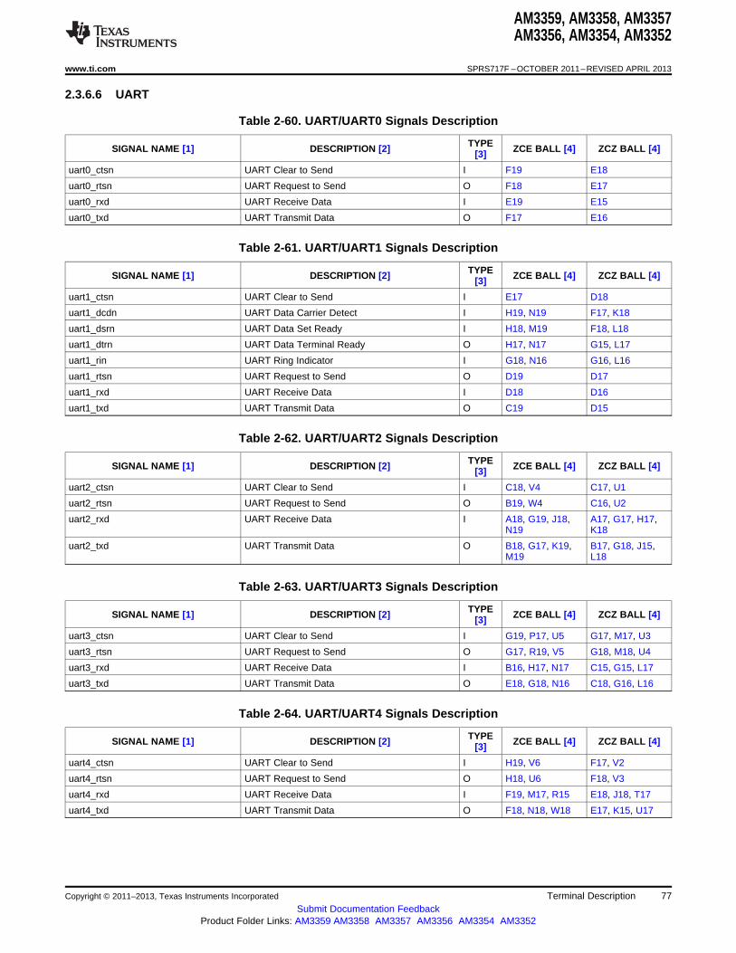
AM3359, AM3358, AM3357AM3356, AM3354, AM3352
www.ti.com SPRS717F –OCTOBER 2011–REVISED APRIL 2013
2.3.6.6 UART
Table 2-60. UART/UART0 Signals Description
TYPESIGNAL NAME [1] DESCRIPTION [2] ZCE BALL [4] ZCZ BALL [4][3]
uart0_ctsn UART Clear to Send I F19 E18
uart0_rtsn UART Request to Send O F18 E17
uart0_rxd UART Receive Data I E19 E15
uart0_txd UART Transmit Data O F17 E16
Table 2-61. UART/UART1 Signals Description
TYPESIGNAL NAME [1] DESCRIPTION [2] ZCE BALL [4] ZCZ BALL [4][3]
uart1_ctsn UART Clear to Send I E17 D18
uart1_dcdn UART Data Carrier Detect I H19, N19 F17, K18
uart1_dsrn UART Data Set Ready I H18, M19 F18, L18
uart1_dtrn UART Data Terminal Ready O H17, N17 G15, L17
uart1_rin UART Ring Indicator I G18, N16 G16, L16
uart1_rtsn UART Request to Send O D19 D17
uart1_rxd UART Receive Data I D18 D16
uart1_txd UART Transmit Data O C19 D15
Table 2-62. UART/UART2 Signals Description
TYPESIGNAL NAME [1] DESCRIPTION [2] ZCE BALL [4] ZCZ BALL [4][3]
uart2_ctsn UART Clear to Send I C18, V4 C17, U1
uart2_rtsn UART Request to Send O B19, W4 C16, U2
uart2_rxd UART Receive Data I A18, G19, J18, A17, G17, H17,N19 K18
uart2_txd UART Transmit Data O B18, G17, K19, B17, G18, J15,M19 L18
Table 2-63. UART/UART3 Signals Description
TYPESIGNAL NAME [1] DESCRIPTION [2] ZCE BALL [4] ZCZ BALL [4][3]
uart3_ctsn UART Clear to Send I G19, P17, U5 G17, M17, U3
uart3_rtsn UART Request to Send O G17, R19, V5 G18, M18, U4
uart3_rxd UART Receive Data I B16, H17, N17 C15, G15, L17
uart3_txd UART Transmit Data O E18, G18, N16 C18, G16, L16
Table 2-64. UART/UART4 Signals Description
TYPESIGNAL NAME [1] DESCRIPTION [2] ZCE BALL [4] ZCZ BALL [4][3]
uart4_ctsn UART Clear to Send I H19, V6 F17, V2
uart4_rtsn UART Request to Send O H18, U6 F18, V3
uart4_rxd UART Receive Data I F19, M17, R15 E18, J18, T17
uart4_txd UART Transmit Data O F18, N18, W18 E17, K15, U17
Copyright © 2011–2013, Texas Instruments Incorporated Terminal Description 77Submit Documentation Feedback
Product Folder Links: AM3359 AM3358 AM3357 AM3356 AM3354 AM3352
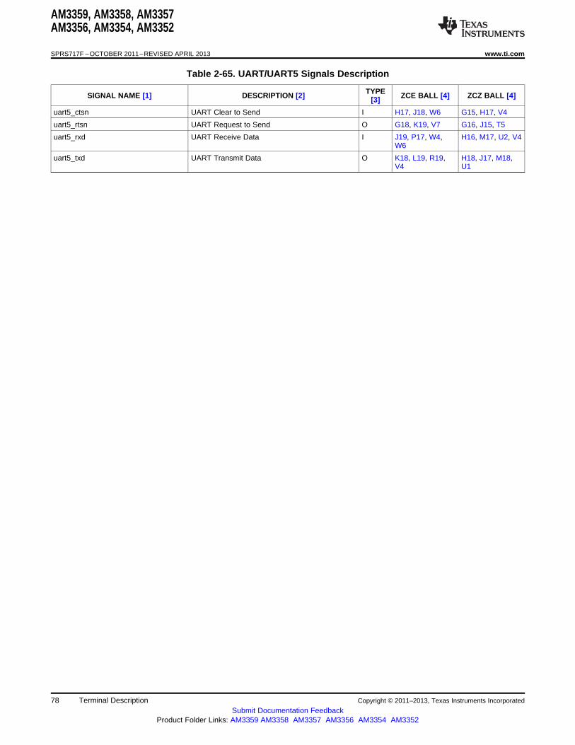
AM3359, AM3358, AM3357AM3356, AM3354, AM3352
SPRS717F –OCTOBER 2011–REVISED APRIL 2013 www.ti.com
Table 2-65. UART/UART5 Signals Description
TYPESIGNAL NAME [1] DESCRIPTION [2] ZCE BALL [4] ZCZ BALL [4][3]
uart5_ctsn UART Clear to Send I H17, J18, W6 G15, H17, V4
uart5_rtsn UART Request to Send O G18, K19, V7 G16, J15, T5
uart5_rxd UART Receive Data I J19, P17, W4, H16, M17, U2, V4W6
uart5_txd UART Transmit Data O K18, L19, R19, H18, J17, M18,V4 U1
78 Terminal Description Copyright © 2011–2013, Texas Instruments Incorporated
Submit Documentation FeedbackProduct Folder Links: AM3359 AM3358 AM3357 AM3356 AM3354 AM3352
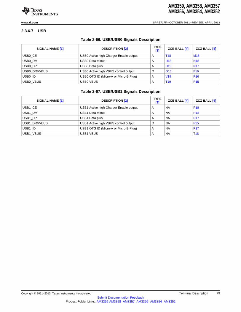
AM3359, AM3358, AM3357AM3356, AM3354, AM3352
www.ti.com SPRS717F –OCTOBER 2011–REVISED APRIL 2013
2.3.6.7 USB
Table 2-66. USB/USB0 Signals Description
TYPESIGNAL NAME [1] DESCRIPTION [2] ZCE BALL [4] ZCZ BALL [4][3]
USB0_CE USB0 Active high Charger Enable output A T18 M15
USB0_DM USB0 Data minus A U18 N18
USB0_DP USB0 Data plus A U19 N17
USB0_DRVVBUS USB0 Active high VBUS control output O G16 F16
USB0_ID USB0 OTG ID (Micro-A or Micro-B Plug) A V19 P16
USB0_VBUS USB0 VBUS A T19 P15
Table 2-67. USB/USB1 Signals Description
TYPESIGNAL NAME [1] DESCRIPTION [2] ZCE BALL [4] ZCZ BALL [4][3]
USB1_CE USB1 Active high Charger Enable output A NA P18
USB1_DM USB1 Data minus A NA R18
USB1_DP USB1 Data plus A NA R17
USB1_DRVVBUS USB1 Active high VBUS control output O NA F15
USB1_ID USB1 OTG ID (Micro-A or Micro-B Plug) A NA P17
USB1_VBUS USB1 VBUS A NA T18
Copyright © 2011–2013, Texas Instruments Incorporated Terminal Description 79Submit Documentation Feedback
Product Folder Links: AM3359 AM3358 AM3357 AM3356 AM3354 AM3352
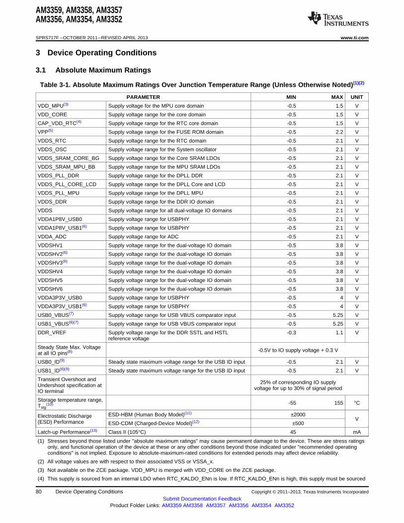
AM3359, AM3358, AM3357AM3356, AM3354, AM3352
SPRS717F –OCTOBER 2011–REVISED APRIL 2013 www.ti.com
3 Device Operating Conditions
3.1 Absolute Maximum Ratings
Table 3-1. Absolute Maximum Ratings Over Junction Temperature Range (Unless Otherwise Noted)(1)(2)
PARAMETER MIN MAX UNIT
VDD_MPU(3) Supply voltage for the MPU core domain -0.5 1.5 V
VDD_CORE Supply voltage range for the core domain -0.5 1.5 V
CAP_VDD_RTC(4) Supply voltage range for the RTC core domain -0.5 1.5 V
VPP(5) Supply voltage range for the FUSE ROM domain -0.5 2.2 V
VDDS_RTC Supply voltage range for the RTC domain -0.5 2.1 V
VDDS_OSC Supply voltage range for the System oscillator -0.5 2.1 V
VDDS_SRAM_CORE_BG Supply voltage range for the Core SRAM LDOs -0.5 2.1 V
VDDS_SRAM_MPU_BB Supply voltage range for the MPU SRAM LDOs -0.5 2.1 V
VDDS_PLL_DDR Supply voltage range for the DPLL DDR -0.5 2.1 V
VDDS_PLL_CORE_LCD Supply voltage range for the DPLL Core and LCD -0.5 2.1 V
VDDS_PLL_MPU Supply voltage range for the DPLL MPU -0.5 2.1 V
VDDS_DDR Supply voltage range for the DDR IO domain -0.5 2.1 V
VDDS Supply voltage range for all dual-voltage IO domains -0.5 2.1 V
VDDA1P8V_USB0 Supply voltage range for USBPHY -0.5 2.1 V
VDDA1P8V_USB1(6) Supply voltage range for USBPHY -0.5 2.1 V
VDDA_ADC Supply voltage range for ADC -0.5 2.1 V
VDDSHV1 Supply voltage range for the dual-voltage IO domain -0.5 3.8 V
VDDSHV2(6) Supply voltage range for the dual-voltage IO domain -0.5 3.8 V
VDDSHV3(6) Supply voltage range for the dual-voltage IO domain -0.5 3.8 V
VDDSHV4 Supply voltage range for the dual-voltage IO domain -0.5 3.8 V
VDDSHV5 Supply voltage range for the dual-voltage IO domain -0.5 3.8 V
VDDSHV6 Supply voltage range for the dual-voltage IO domain -0.5 3.8 V
VDDA3P3V_USB0 Supply voltage range for USBPHY -0.5 4 V
VDDA3P3V_USB1(6) Supply voltage range for USBPHY -0.5 4 V
USB0_VBUS(7) Supply voltage range for USB VBUS comparator input -0.5 5.25 V
USB1_VBUS(6)(7) Supply voltage range for USB VBUS comparator input -0.5 5.25 V
DDR_VREF Supply voltage range for the DDR SSTL and HSTL -0.3 1.1 Vreference voltage
Steady State Max. Voltage -0.5V to IO supply voltage + 0.3 Vat all IO pins(8)
USB0_ID(9) Steady state maximum voltage range for the USB ID input -0.5 2.1 V
USB1_ID(6)(9) Steady state maximum voltage range for the USB ID input -0.5 2.1 V
Transient Overshoot and 25% of corresponding IO supplyUndershoot specification at voltage for up to 30% of signal periodIO terminal
Storage temperature range, -55 155 °CTstg(10)
ESD-HBM (Human Body Model)(11) ±2000Electrostatic Discharge V(ESD) Performance ESD-CDM (Charged-Device Model)(12) ±500
Latch-up Performance(13) Class II (105°C) 45 mA
(1) Stresses beyond those listed under "absolute maximum ratings" may cause permanent damage to the device. These are stress ratingsonly, and functional operation of the device at these or any other conditions beyond those indicated under "recommended operatingconditions" is not implied. Exposure to absolute-maximum-rated conditions for extended periods may affect device reliability.
(2) All voltage values are with respect to their associated VSS or VSSA_x.
(3) Not available on the ZCE package. VDD_MPU is merged with VDD_CORE on the ZCE package.
(4) This supply is sourced from an internal LDO when RTC_KALDO_ENn is low. If RTC_KALDO_ENn is high, this supply must be sourced
80 Device Operating Conditions Copyright © 2011–2013, Texas Instruments Incorporated
Submit Documentation FeedbackProduct Folder Links: AM3359 AM3358 AM3357 AM3356 AM3354 AM3352
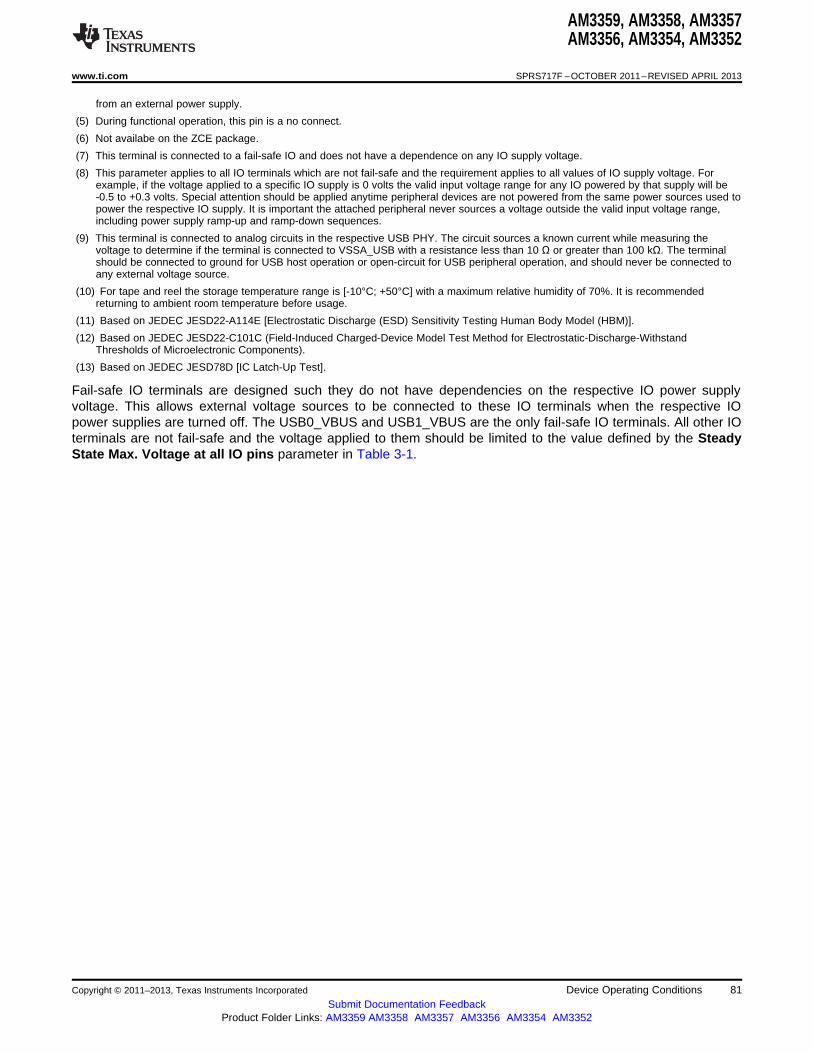
AM3359, AM3358, AM3357AM3356, AM3354, AM3352
www.ti.com SPRS717F –OCTOBER 2011–REVISED APRIL 2013
from an external power supply.
(5) During functional operation, this pin is a no connect.
(6) Not availabe on the ZCE package.
(7) This terminal is connected to a fail-safe IO and does not have a dependence on any IO supply voltage.
(8) This parameter applies to all IO terminals which are not fail-safe and the requirement applies to all values of IO supply voltage. Forexample, if the voltage applied to a specific IO supply is 0 volts the valid input voltage range for any IO powered by that supply will be‑0.5 to +0.3 volts. Special attention should be applied anytime peripheral devices are not powered from the same power sources used topower the respective IO supply. It is important the attached peripheral never sources a voltage outside the valid input voltage range,including power supply ramp-up and ramp-down sequences.
(9) This terminal is connected to analog circuits in the respective USB PHY. The circuit sources a known current while measuring thevoltage to determine if the terminal is connected to VSSA_USB with a resistance less than 10 Ω or greater than 100 kΩ. The terminalshould be connected to ground for USB host operation or open-circuit for USB peripheral operation, and should never be connected toany external voltage source.
(10) For tape and reel the storage temperature range is [-10°C; +50°C] with a maximum relative humidity of 70%. It is recommendedreturning to ambient room temperature before usage.
(11) Based on JEDEC JESD22-A114E [Electrostatic Discharge (ESD) Sensitivity Testing Human Body Model (HBM)].
(12) Based on JEDEC JESD22-C101C (Field-Induced Charged-Device Model Test Method for Electrostatic-Discharge-WithstandThresholds of Microelectronic Components).
(13) Based on JEDEC JESD78D [IC Latch-Up Test].
Fail-safe IO terminals are designed such they do not have dependencies on the respective IO power supplyvoltage. This allows external voltage sources to be connected to these IO terminals when the respective IOpower supplies are turned off. The USB0_VBUS and USB1_VBUS are the only fail-safe IO terminals. All other IOterminals are not fail-safe and the voltage applied to them should be limited to the value defined by the SteadyState Max. Voltage at all IO pins parameter in Table 3-1.
Copyright © 2011–2013, Texas Instruments Incorporated Device Operating Conditions 81Submit Documentation Feedback
Product Folder Links: AM3359 AM3358 AM3357 AM3356 AM3354 AM3352

AM3359, AM3358, AM3357AM3356, AM3354, AM3352
SPRS717F –OCTOBER 2011–REVISED APRIL 2013 www.ti.com
3.2 Recommended Operating Conditions
Device Operating Performance Points are defined in Table 3-2 through Table 3-9.
Table 3-2. VDD_CORE Operating Performance Points for ZCZ Packagewith Device Revision Code "Blank"(1)
VDD_CORE VDD_COREOPP DDR3, DDR2(2) mDDR(2) L3 and L4Device Rev. DDR3L(2)
MIN NOM MAX"Blank"
OPP100 1.056 V 1.100 V 1.144 V 400 MHz 266 MHz 200 MHz 200 MHz and100 MHz
OPP50 0.912 V 0.950 V 0.988 V - 125 MHz 90 MHz 100 MHz and50 MHz
(1) Frequencies in this table indicate maximum performance for a given OPP condition.
(2) This parameter represents the maximum memory clock frequency. Since data is transferred on both edges of the clock, double-data rate(DDR), the maximum data rate is two times the maximum memory clock frequency defined in this table.
Table 3-3. VDD_MPU Operating Performance Points for ZCZ Packagewith Device Revision Code "Blank"(1)
VDD_MPUVDD_MPU OPP ARM (A8)Device Rev. "Blank" MIN NOM MAX
Turbo 1.210 V 1.260 V 1.326 V 720 MHz
OPP120 1.152 V 1.200 V 1.248 V 600 MHz
OPP100(2) 1.056 V 1.100 V 1.144 V 500 MHz
OPP100(3) 1.056 V 1.100 V 1.144 V 275 MHz
(1) Frequencies in this table indicate maximum performance for a given OPP condition.
(2) Applies to all orderable AM335_ZCZ_50 (500-MHz speed grade) or higher devices.
(3) Applies to all orderable AM335_ZCZ_27 (275-MHz speed grade) devices.
Table 3-4. Valid Combinations of VDD_CORE andVDD_MPU Operating Performance Points for ZCZ
Package with Device Revision Code "Blank"
VDD_CORE VDD_MPU
OPP50 OPP100
OPP100 OPP100
OPP100 OPP120
OPP100 Turbo
82 Device Operating Conditions Copyright © 2011–2013, Texas Instruments Incorporated
Submit Documentation FeedbackProduct Folder Links: AM3359 AM3358 AM3357 AM3356 AM3354 AM3352
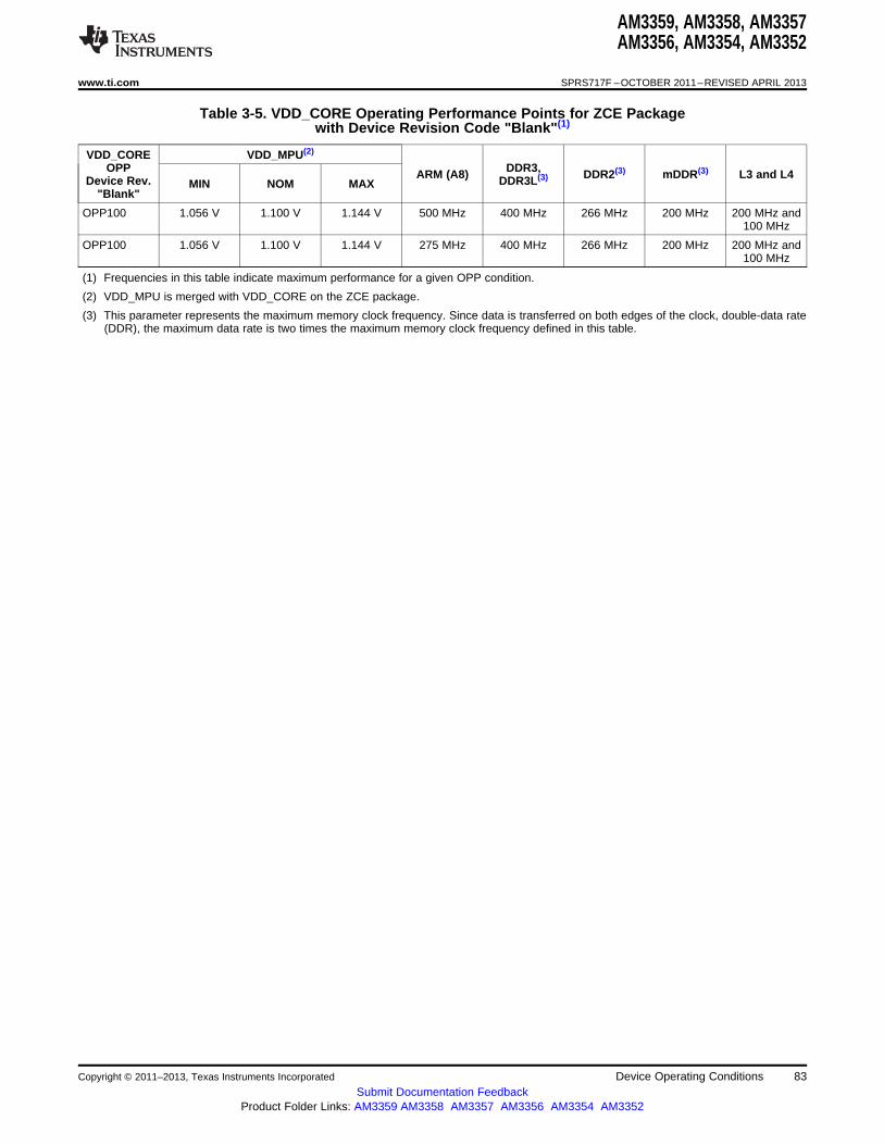
AM3359, AM3358, AM3357AM3356, AM3354, AM3352
www.ti.com SPRS717F –OCTOBER 2011–REVISED APRIL 2013
Table 3-5. VDD_CORE Operating Performance Points for ZCE Packagewith Device Revision Code "Blank"(1)
VDD_CORE VDD_MPU(2)
OPP DDR3,ARM (A8) DDR2(3) mDDR(3) L3 and L4Device Rev. DDR3L(3)MIN NOM MAX
"Blank"
OPP100 1.056 V 1.100 V 1.144 V 500 MHz 400 MHz 266 MHz 200 MHz 200 MHz and100 MHz
OPP100 1.056 V 1.100 V 1.144 V 275 MHz 400 MHz 266 MHz 200 MHz 200 MHz and100 MHz
(1) Frequencies in this table indicate maximum performance for a given OPP condition.
(2) VDD_MPU is merged with VDD_CORE on the ZCE package.
(3) This parameter represents the maximum memory clock frequency. Since data is transferred on both edges of the clock, double-data rate(DDR), the maximum data rate is two times the maximum memory clock frequency defined in this table.
Copyright © 2011–2013, Texas Instruments Incorporated Device Operating Conditions 83Submit Documentation Feedback
Product Folder Links: AM3359 AM3358 AM3357 AM3356 AM3354 AM3352

AM3359, AM3358, AM3357AM3356, AM3354, AM3352
SPRS717F –OCTOBER 2011–REVISED APRIL 2013 www.ti.com
Table 3-6. VDD_CORE Operating Performance Points for ZCZ Packagewith Device Revision Code "A" or Newer(1)
VDD_CORE VDD_COREOPP DDR3, DDR2(2) mDDR(2) L3 and L4Rev "A" or DDR3L(2)
MIN NOM MAXNewer
OPP100 1.056 V 1.100 V 1.144 V 400 MHz 266 MHz 200 MHz 200 MHz and100 MHz
OPP50 0.912 V 0.950 V 0.988 V - 125 MHz 90 MHz 100 MHz and50 MHz
(1) Frequencies in this table indicate maximum performance for a given OPP condition.
(2) This parameter represents the maximum memory clock frequency. Since data is transferred on both edges of the clock, double-data rate(DDR), the maximum data rate is two times the maximum memory clock frequency defined in this table.
Table 3-7. VDD_MPU Operating Performance Points for ZCZ Packagewith Device Revision Code "A" or Newer(1)
VDD_MPUVDD_MPU OPP ARM (A8)Rev "A" or Newer MIN NOM MAX
Nitro 1.272 V 1.325 V 1.378 V 1 GHz
Turbo 1.210 V 1.260 V 1.326 V 800 MHz
OPP120 1.152 V 1.200 V 1.248 V 720 MHz
OPP100(2) 1.056 V 1.100 V 1.144 V 600 MHz
OPP100(3) 1.056 V 1.100 V 1.144 V 300 MHz
OPP50 0.912 V 0.950 V 0.988 V 300 MHz
(1) Frequencies in this table indicate maximum performance for a given OPP condition.
(2) Applies to all orderable AM335__ZCZ_60 (600 MHz speed grade) or higher devices.
(3) Applies to all orderable AM335__ZCZ_30 (300 MHz speed grade) devices.
Table 3-8. Valid Combinations of VDD_CORE andVDD_MPU Operating Performance Points for ZCZPackage with Device Revision Code "A" or Newer
VDD_CORE VDD_MPU
OPP50 OPP50
OPP50 OPP100
OPP100 OPP50
OPP100 OPP100
OPP100 OPP120
OPP100 Turbo
OPP100 Nitro
84 Device Operating Conditions Copyright © 2011–2013, Texas Instruments Incorporated
Submit Documentation FeedbackProduct Folder Links: AM3359 AM3358 AM3357 AM3356 AM3354 AM3352
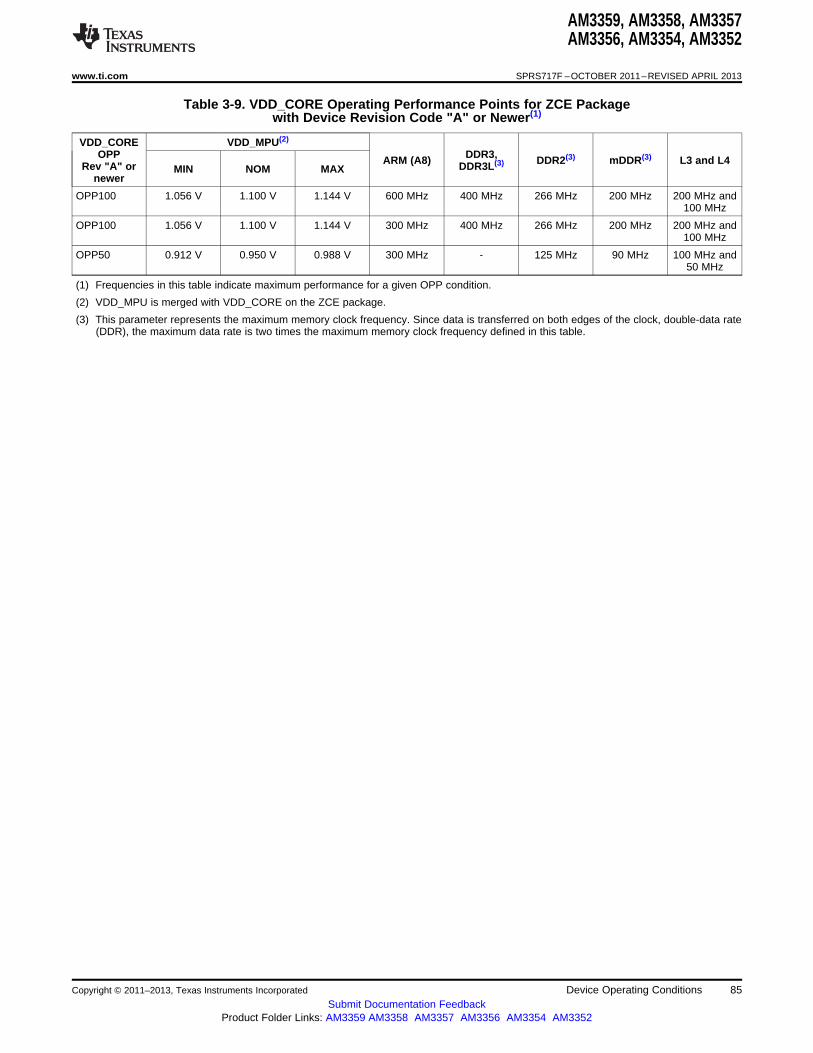
AM3359, AM3358, AM3357AM3356, AM3354, AM3352
www.ti.com SPRS717F –OCTOBER 2011–REVISED APRIL 2013
Table 3-9. VDD_CORE Operating Performance Points for ZCE Packagewith Device Revision Code "A" or Newer(1)
VDD_CORE VDD_MPU(2)
OPP DDR3,ARM (A8) DDR2(3) mDDR(3) L3 and L4Rev "A" or DDR3L(3)MIN NOM MAX
newer
OPP100 1.056 V 1.100 V 1.144 V 600 MHz 400 MHz 266 MHz 200 MHz 200 MHz and100 MHz
OPP100 1.056 V 1.100 V 1.144 V 300 MHz 400 MHz 266 MHz 200 MHz 200 MHz and100 MHz
OPP50 0.912 V 0.950 V 0.988 V 300 MHz - 125 MHz 90 MHz 100 MHz and50 MHz
(1) Frequencies in this table indicate maximum performance for a given OPP condition.
(2) VDD_MPU is merged with VDD_CORE on the ZCE package.
(3) This parameter represents the maximum memory clock frequency. Since data is transferred on both edges of the clock, double-data rate(DDR), the maximum data rate is two times the maximum memory clock frequency defined in this table.
Copyright © 2011–2013, Texas Instruments Incorporated Device Operating Conditions 85Submit Documentation Feedback
Product Folder Links: AM3359 AM3358 AM3357 AM3356 AM3354 AM3352
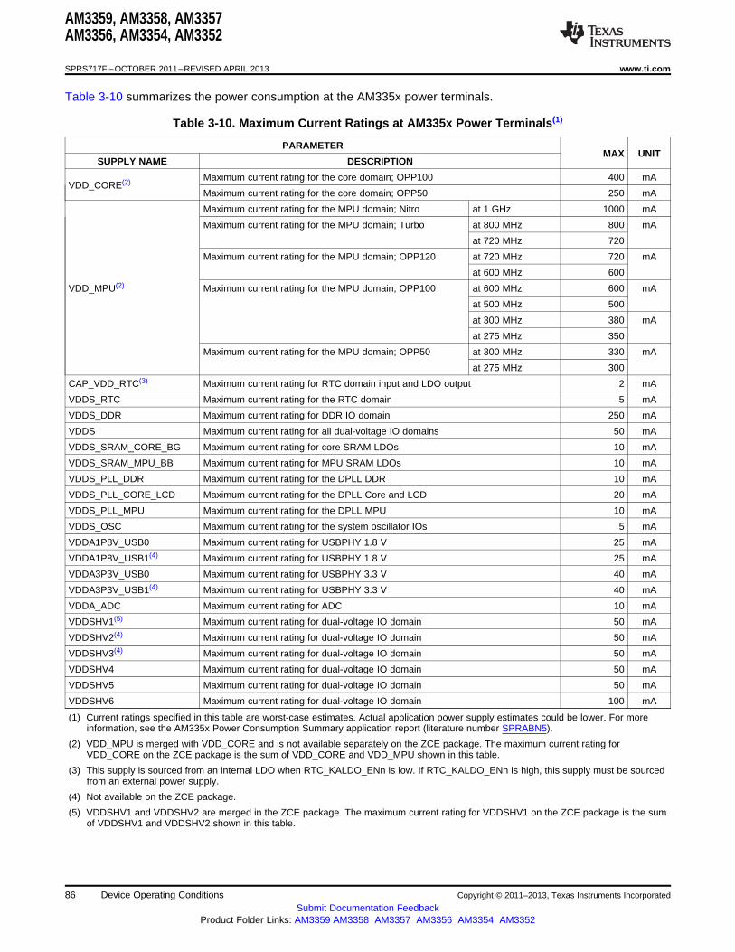
AM3359, AM3358, AM3357AM3356, AM3354, AM3352
SPRS717F –OCTOBER 2011–REVISED APRIL 2013 www.ti.com
Table 3-10 summarizes the power consumption at the AM335x power terminals.
Table 3-10. Maximum Current Ratings at AM335x Power Terminals(1)
PARAMETERMAX UNIT
SUPPLY NAME DESCRIPTION
Maximum current rating for the core domain; OPP100 400 mAVDD_CORE(2)
Maximum current rating for the core domain; OPP50 250 mA
Maximum current rating for the MPU domain; Nitro at 1 GHz 1000 mA
Maximum current rating for the MPU domain; Turbo at 800 MHz 800 mA
at 720 MHz 720
Maximum current rating for the MPU domain; OPP120 at 720 MHz 720 mA
at 600 MHz 600
VDD_MPU(2) Maximum current rating for the MPU domain; OPP100 at 600 MHz 600 mA
at 500 MHz 500
at 300 MHz 380 mA
at 275 MHz 350
Maximum current rating for the MPU domain; OPP50 at 300 MHz 330 mA
at 275 MHz 300
CAP_VDD_RTC(3) Maximum current rating for RTC domain input and LDO output 2 mA
VDDS_RTC Maximum current rating for the RTC domain 5 mA
VDDS_DDR Maximum current rating for DDR IO domain 250 mA
VDDS Maximum current rating for all dual-voltage IO domains 50 mA
VDDS_SRAM_CORE_BG Maximum current rating for core SRAM LDOs 10 mA
VDDS_SRAM_MPU_BB Maximum current rating for MPU SRAM LDOs 10 mA
VDDS_PLL_DDR Maximum current rating for the DPLL DDR 10 mA
VDDS_PLL_CORE_LCD Maximum current rating for the DPLL Core and LCD 20 mA
VDDS_PLL_MPU Maximum current rating for the DPLL MPU 10 mA
VDDS_OSC Maximum current rating for the system oscillator IOs 5 mA
VDDA1P8V_USB0 Maximum current rating for USBPHY 1.8 V 25 mA
VDDA1P8V_USB1(4) Maximum current rating for USBPHY 1.8 V 25 mA
VDDA3P3V_USB0 Maximum current rating for USBPHY 3.3 V 40 mA
VDDA3P3V_USB1(4) Maximum current rating for USBPHY 3.3 V 40 mA
VDDA_ADC Maximum current rating for ADC 10 mA
VDDSHV1(5) Maximum current rating for dual-voltage IO domain 50 mA
VDDSHV2(4) Maximum current rating for dual-voltage IO domain 50 mA
VDDSHV3(4) Maximum current rating for dual-voltage IO domain 50 mA
VDDSHV4 Maximum current rating for dual-voltage IO domain 50 mA
VDDSHV5 Maximum current rating for dual-voltage IO domain 50 mA
VDDSHV6 Maximum current rating for dual-voltage IO domain 100 mA
(1) Current ratings specified in this table are worst-case estimates. Actual application power supply estimates could be lower. For moreinformation, see the AM335x Power Consumption Summary application report (literature number SPRABN5).
(2) VDD_MPU is merged with VDD_CORE and is not available separately on the ZCE package. The maximum current rating forVDD_CORE on the ZCE package is the sum of VDD_CORE and VDD_MPU shown in this table.
(3) This supply is sourced from an internal LDO when RTC_KALDO_ENn is low. If RTC_KALDO_ENn is high, this supply must be sourcedfrom an external power supply.
(4) Not available on the ZCE package.
(5) VDDSHV1 and VDDSHV2 are merged in the ZCE package. The maximum current rating for VDDSHV1 on the ZCE package is the sumof VDDSHV1 and VDDSHV2 shown in this table.
86 Device Operating Conditions Copyright © 2011–2013, Texas Instruments Incorporated
Submit Documentation FeedbackProduct Folder Links: AM3359 AM3358 AM3357 AM3356 AM3354 AM3352

AM3359, AM3358, AM3357AM3356, AM3354, AM3352
www.ti.com SPRS717F –OCTOBER 2011–REVISED APRIL 2013
The power-on hours (POH) information in Table 3-11 is provided solely for your convenience and does notextend or modify the warranty provided under TI's standard terms and conditions for TI semiconductor products.
To avoid significant degradation, the device power-on hours (POH) must be limited to the following:
Table 3-11. Reliability Data
COMMERCIAL INDUSTRIAL EXTENDEDOPERATING
JUNCTION TEMP LIFETIME JUNCTION TEMP LIFETIME JUNCTION TEMP LIFETIMECONDITION(Tj) (POH)(1) (Tj) (POH)(1) (Tj) (POH)(1)
Nitro 0°C to 90°C 100K -40°C to 90°C 100K -40°C to 105°C 37K
Turbo 0°C to 90°C 100K -40°C to 90°C 100K -40°C to 105°C 80K
OPP120 0°C to 90°C 100K -40°C to 90°C 100K -40°C to 105°C 100K
OPP100 0°C to 90°C 100K -40°C to 90°C 100K -40°C to 105°C 100K
OPP50 0°C to 90°C 100K -40°C to 90°C 100K -40°C to 105°C 100K
(1) POH = Power-on hours when the device is fully functional.
NOTELogic functions and parameter values are not assured out of the range specified in therecommended operating conditions.
The above notations cannot be deemed a warranty or deemed to extend or modify the warranty under TI'sstandard terms and conditions for TI semiconductor products.
The device is used under the recommended operating conditions described in Table 3-12.
Table 3-12. Recommended Operating Conditions
PARAMETERMIN NOM MAX UNIT
SUPPLY NAME DESCRIPTION
Supply voltage range for core 1.056 1.100 1.144domain; OPP100VDD_CORE(1) V
Supply voltage range for core 0.912 0.950 0.988domain; OPP50
Supply voltage range for MPU 1.272 1.325 1.378domain, Nitro
Supply voltage range for MPU 1.210 1.260 1.326domain; Turbo
Supply voltage range for MPUVDD_MPU(1)(2) 1.152 1.200 1.248 Vdomain; OPP120
Supply voltage range for MPU 1.056 1.100 1.144domain; OPP100
Supply voltage range for MPU 0.912 0.950 0.988domain; OPP50
Supply voltage range for RTCCAP_VDD_RTC(3) 0.900 1.100 1.250 Vdomain input
Supply voltage range for RTCVDDS_RTC 1.710 1.800 1.890 Vdomain
Supply voltage range for DDR IO 1.710 1.800 1.890domain (DDR2)
Supply voltage range for DDR IOVDDS_DDR 1.425 1.500 1.575 Vdomain (DDR3)
Supply voltage range for DDR IO 1.283 1.350 1.418domain (DDR3L)
Supply voltage range for all dual-VDDS(4) 1.710 1.800 1.890 Vvoltage IO domains
Supply voltage range for CoreVDDS_SRAM_CORE_BG 1.710 1.800 1.890 VSRAM LDOs, Analog
Copyright © 2011–2013, Texas Instruments Incorporated Device Operating Conditions 87Submit Documentation Feedback
Product Folder Links: AM3359 AM3358 AM3357 AM3356 AM3354 AM3352
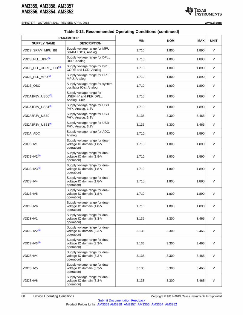
AM3359, AM3358, AM3357AM3356, AM3354, AM3352
SPRS717F –OCTOBER 2011–REVISED APRIL 2013 www.ti.com
Table 3-12. Recommended Operating Conditions (continued)
PARAMETERMIN NOM MAX UNIT
SUPPLY NAME DESCRIPTION
Supply voltage range for MPUVDDS_SRAM_MPU_BB 1.710 1.800 1.890 VSRAM LDOs, Analog
Supply voltage range for DPLLVDDS_PLL_DDR(5) 1.710 1.800 1.890 VDDR, Analog
Supply voltage range for DPLLVDDS_PLL_CORE_LCD(5) 1.710 1.800 1.890 VCORE and LCD, Analog
Supply voltage range for DPLLVDDS_PLL_MPU(5) 1.710 1.800 1.890 VMPU, Analog
Supply voltage range for systemVDDS_OSC 1.710 1.800 1.890 Voscillator IO's, Analog
Supply voltage range forVDDA1P8V_USB0(5) USBPHY and PER DPLL, 1.710 1.800 1.890 V
Analog, 1.8V
Supply voltage range for USBVDDA1P8V_USB1(6) 1.710 1.800 1.890 VPHY, Analog, 1.8V
Supply voltage range for USBVDDA3P3V_USB0 3.135 3.300 3.465 VPHY, Analog, 3.3V
Supply voltage range for USBVDDA3P3V_USB1(6) 3.135 3.300 3.465 VPHY, Analog, 3.3V
Supply voltage range for ADC,VDDA_ADC 1.710 1.800 1.890 VAnalog
Supply voltage range for dual-VDDSHV1 voltage IO domain (1.8-V 1.710 1.800 1.890 V
operation)
Supply voltage range for dual-VDDSHV2(6) voltage IO domain (1.8-V 1.710 1.800 1.890 V
operation)
Supply voltage range for dual-VDDSHV3(6) voltage IO domain (1.8-V 1.710 1.800 1.890 V
operation)
Supply voltage range for dual-VDDSHV4 voltage IO domain (1.8-V 1.710 1.800 1.890 V
operation)
Supply voltage range for dual-VDDSHV5 voltage IO domain (1.8-V 1.710 1.800 1.890 V
operation)
Supply voltage range for dual-VDDSHV6 voltage IO domain (1.8-V 1.710 1.800 1.890 V
operation)
Supply voltage range for dual-VDDSHV1 voltage IO domain (3.3-V 3.135 3.300 3.465 V
operation)
Supply voltage range for dual-VDDSHV2(6) voltage IO domain (3.3-V 3.135 3.300 3.465 V
operation)
Supply voltage range for dual-VDDSHV3(6) voltage IO domain (3.3-V 3.135 3.300 3.465 V
operation)
Supply voltage range for dual-VDDSHV4 voltage IO domain (3.3-V 3.135 3.300 3.465 V
operation)
Supply voltage range for dual-VDDSHV5 voltage IO domain (3.3-V 3.135 3.300 3.465 V
operation)
Supply voltage range for dual-VDDSHV6 voltage IO domain (3.3-V 3.135 3.300 3.465 V
operation)
88 Device Operating Conditions Copyright © 2011–2013, Texas Instruments Incorporated
Submit Documentation FeedbackProduct Folder Links: AM3359 AM3358 AM3357 AM3356 AM3354 AM3352

AM3359, AM3358, AM3357AM3356, AM3354, AM3352
www.ti.com SPRS717F –OCTOBER 2011–REVISED APRIL 2013
Table 3-12. Recommended Operating Conditions (continued)
PARAMETERMIN NOM MAX UNIT
SUPPLY NAME DESCRIPTION
Voltage range for DDR SSTL andDDR_VREF HSTL reference input (DDR2, 0.49*VDDS_DDR 0.50*VDDS_DDR 0.51*VDDS_DDR V
DDR3, DDR3L)
Voltage range for USB VBUSUSB0_VBUS 0.000 5.000 5.250 Vcomparator input
Voltage range for USB VBUSUSB1_VBUS(6) 0.000 5.000 5.250 Vcomparator input
Voltage range for the USB IDUSB0_ID (7) Vinput
Voltage range for the USB IDUSB1_ID(6) (7) Vinput
Commercial Temperature 0 90Operating Temperature Industrial Temperature -40 90 °CRange, Tj
Extended Temperature -40 105
(1) The supply voltage defined by OPP100 should be applied to this power domain before the device is released from reset.
(2) Not available on the ZCE package. VDD_MPU is merged with VDD_CORE on the ZCE package.
(3) This supply is sourced from an internal LDO when RTC_KALDO_ENn is low. If RTC_KALDO_ENn is high, this supply must be sourcedfrom an external power supply.
(4) VDDS should be supplied irrespective of 1.8-V or 3.3-V mode of operation of the dual-voltage IOs.
(5) For more details on power supply requirements, see Section 4.1.4.
(6) Not available on the ZCE package.
(7) This terminal is connected to analog circuits in the respective USB PHY. The circuit sources a known current while measuring thevoltage to determine if the terminal is connected to VSSA_USB with a resistance less than 10 Ω or greater than 100 kΩ. The terminalshould be connected to ground for USB host operation or open-circuit for USB peripheral operation, and should never be connected toany external voltage source.
Copyright © 2011–2013, Texas Instruments Incorporated Device Operating Conditions 89Submit Documentation Feedback
Product Folder Links: AM3359 AM3358 AM3357 AM3356 AM3354 AM3352

AM3359, AM3358, AM3357AM3356, AM3354, AM3352
SPRS717F –OCTOBER 2011–REVISED APRIL 2013 www.ti.com
3.3 DC Electrical Characteristics
Table 3-13 summarizes the dc electrical characteristics.
Note: The interfaces or signals described in Table 3-13 correspond to the interfaces or signals available inmultiplexing mode 0. All interfaces or signals multiplexed on the terminals described in Table 3-13 have the samedc electrical characteristics.
Table 3-13. DC Electrical Characteristics Over Recommended Ranges of Supply Voltage and OperatingTemperature (Unless Otherwise Noted)
PARAMETER MIN NOM MAX UNIT
DDR_RESETn,DDR_CSn0,DDR_CKE,DDR_CK,DDR_CKn,DDR_CASn,DDR_RASn,DDR_WEn,DDR_BA0,DDR_BA1,DDR_BA2,DDR_A0,DDR_A1,DDR_A2,DDR_A3,DDR_A4,DDR_A5,DDR_A6,DDR_A7,DDR_A8,DDR_A9,DDR_A10,DDR_A11,DDR_A12,DDR_A13,DDR_A14,DDR_A15,DDR_ODT,DDR_D0,DDR_D1,DDR_D2,DDR_D3,DDR_D4,DDR_D5,DDR_D6,DDR_D7,DDR_D8,DDR_D9,DDR_D10,DDR_D11,DDR_D12,DDR_D13,DDR_D14,DDR_D15,DDR_DQM0,DDR_DQM1,DDR_DQS0,DDR_DQSn0,DDR_DQS1,DDR_DQSn1 pins(mDDR - LVCMOS mode)
0.65 *VIH High-level input voltage VVDDS_DDR
0.35 *VIL Low-level input voltage VVDDS_DDR
VHYS Hysteresis voltage at an input 0.07 0.25 V
High level output voltage, driver enabled, pullup VDDS_DDR -VOH IOH = 8 mA Vor pulldown disbaled 0.4
Low level output voltage, driver enabled, pullupVOL IOL = 8 mA 0.4 Vor pulldown disbaled
Input leakage current, Receiver disabled, pullup or pulldown 10inhibitedII µAInput leakage current, Receiver disabled, pullup enabled -240 -80
Input leakage current, Receiver disabled, pulldown enabled 80 240
Total leakage current through the terminal connection of a driver-IOZ receiver combination that may include a pullup or pulldown. The 10 µA
driver output is disabled and the pullup or pulldown is inhibited.
DDR_RESETn,DDR_CSn0,DDR_CKE,DDR_CK,DDR_CKn,DDR_CASn,DDR_RASn,DDR_WEn,DDR_BA0,DDR_BA1,DDR_BA2,DDR_A0,DDR_A1,DDR_A2,DDR_A3,DDR_A4,DDR_A5,DDR_A6,DDR_A7,DDR_A8,DDR_A9,DDR_A10,DDR_A11,DDR_A12,DDR_A13,DDR_A14,DDR_A15,DDR_ODT,DDR_D0,DDR_D1,DDR_D2,DDR_D3,DDR_D4,DDR_D5,DDR_D6,DDR_D7,DDR_D8,DDR_D9,DDR_D10,DDR_D11,DDR_D12,DDR_D13,DDR_D14,DDR_D15,DDR_DQM0,DDR_DQM1,DDR_DQS0,DDR_DQSn0,DDR_DQS1,DDR_DQSn1 pins(DDR2 - SSTL mode)
VIH High-level input voltage DDR_VREF + V0.125
VIL Low-level input voltage DDR_VREF - V0.125
VHYS Hysteresis voltage at an input NA V
VOH High-level output voltage, driver enabled, pullup IOH = 8 mA VDDS_DDR - Vor pulldown disbaled 0.4
VOL Low-level output voltage, driver enabled, pullup IOL = 8 mA 0.4 Vor pulldown disbaled
Input leakage current, Receiver disabled, pullup or pulldown 10inhibitedII µAInput leakage current, Receiver disabled, pullup enabled -240 -80
Input leakage current, Receiver disabled, pulldown enabled 80 240
IOZ Total leakage current through the terminal connection of a driver- 10 µAreceiver combination that may include a pullup or pulldown. Thedriver output is disabled and the pullup or pulldown is inhibited.
90 Device Operating Conditions Copyright © 2011–2013, Texas Instruments Incorporated
Submit Documentation FeedbackProduct Folder Links: AM3359 AM3358 AM3357 AM3356 AM3354 AM3352

AM3359, AM3358, AM3357AM3356, AM3354, AM3352
www.ti.com SPRS717F –OCTOBER 2011–REVISED APRIL 2013
Table 3-13. DC Electrical Characteristics Over Recommended Ranges of Supply Voltage and OperatingTemperature (Unless Otherwise Noted) (continued)
PARAMETER MIN NOM MAX UNIT
DDR_RESETn,DDR_CSn0,DDR_CKE,DDR_CK,DDR_CKn,DDR_CASn,DDR_RASn,DDR_WEn,DDR_BA0,DDR_BA1,DDR_BA2,DDR_A0,DDR_A1,DDR_A2,DDR_A3,DDR_A4,DDR_A5,DDR_A6,DDR_A7,DDR_A8,DDR_A9,DDR_A10,DDR_A11,DDR_A12,DDR_A13,DDR_A14,DDR_A15,DDR_ODT,DDR_D0,DDR_D1,DDR_D2,DDR_D3,DDR_D4,DDR_D5,DDR_D6,DDR_D7,DDR_D8,DDR_D9,DDR_D10,DDR_D11,DDR_D12,DDR_D13,DDR_D14,DDR_D15,DDR_DQM0,DDR_DQM1,DDR_DQS0,DDR_DQSn0,DDR_DQS1,DDR_DQSn1 pins(DDR3, DDR3L - HSTL mode)
VIH High-level input voltage VDDS_DDR = DDR_VREF + V1.5 V 0.1
VDDS_DDR = DDR_VREF +1.35 V 0.09
VDDS_DDR = DDR_VREF -1.5 V 0.1
VIL Low-level input voltage VVDDS_DDR = DDR_VREF -1.35 V 0.09
VHYS Hysteresis voltage at an input NA V
VOH High-level output voltage, driver enabled, pullup IOH = 8 mA VDDS_DDR - Vor pulldown disbaled 0.4
VOL Low-level output voltage, driver enabled, pullup IOL = 8 mA 0.4 Vor pulldown disbaled
Input leakage current, Receiver disabled, pullup or pulldown 10inhibitedII µAInput leakage current, Receiver disabled, pullup enabled -240 -80
Input leakage current, Receiver disabled, pulldown enabled 80 240
IOZ Total leakage current through the terminal connection of a driver- 10 µAreceiver combination that may include a pullup or pulldown. Thedriver output is disabled and the pullup or pulldown is inhibited.
ECAP0_IN_PWM0_OUT,UART0_CTSn,UART0_RTSn,UART0_RXD,UART0_TXD,UART1_CTSn,UART1_RTSn,UART1_RXD,UART1_TXD,I2C0_SDA,I2C0_SCL,XDMA_EVENT_INTR0,XDMA_EVENT_INTR1,WARMRSTn,PWRONRSTn,EXTINTn,TMS,TDO,USB0_DRVVBUS,USB1_DRVVBUS (VDDSHV6 = 1.8 V)
0.65 *VIH High-level input voltage VVDDSHV6
0.35 *VIL Low-level input voltage VVDDSHV6
VHYS Hysteresis voltage at an input 0.18 0.305 V
VOH High-level output voltage, driver enabled, pullup IOH = 4 mA VDDSHV6 - Vor pulldown disbaled 0.45
VOL Low-level output voltage, driver enabled, pullup IOL = 4 mA 0.45 Vor pulldown disbaled
Input leakage current, Receiver disabled, pullup or pulldown 8inhibitedII µAInput leakage current, Receiver disabled, pullup enabled -161 -100 -52
Input leakage current, Receiver disabled, pulldown enabled 52 100 170
IOZ Total leakage current through the terminal connection of a driver- 8 µAreceiver combination that may include a pullup or pulldown. Thedriver output is disabled and the pullup or pulldown is inhibited.
Copyright © 2011–2013, Texas Instruments Incorporated Device Operating Conditions 91Submit Documentation Feedback
Product Folder Links: AM3359 AM3358 AM3357 AM3356 AM3354 AM3352
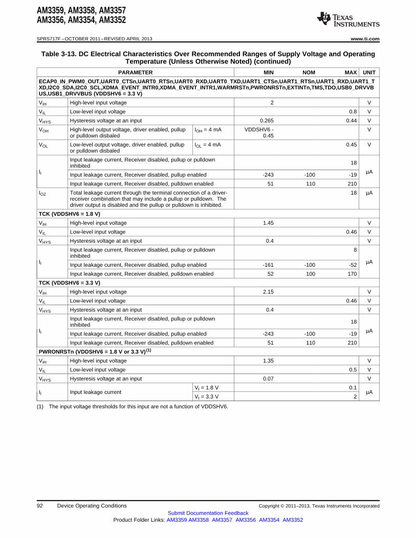
AM3359, AM3358, AM3357AM3356, AM3354, AM3352
SPRS717F –OCTOBER 2011–REVISED APRIL 2013 www.ti.com
Table 3-13. DC Electrical Characteristics Over Recommended Ranges of Supply Voltage and OperatingTemperature (Unless Otherwise Noted) (continued)
PARAMETER MIN NOM MAX UNIT
ECAP0_IN_PWM0_OUT,UART0_CTSn,UART0_RTSn,UART0_RXD,UART0_TXD,UART1_CTSn,UART1_RTSn,UART1_RXD,UART1_TXD,I2C0_SDA,I2C0_SCL,XDMA_EVENT_INTR0,XDMA_EVENT_INTR1,WARMRSTn,PWRONRSTn,EXTINTn,TMS,TDO,USB0_DRVVBUS,USB1_DRVVBUS (VDDSHV6 = 3.3 V)
VIH High-level input voltage 2 V
VIL Low-level input voltage 0.8 V
VHYS Hysteresis voltage at an input 0.265 0.44 V
VOH High-level output voltage, driver enabled, pullup IOH = 4 mA VDDSHV6 - Vor pulldown disbaled 0.45
VOL Low-level output voltage, driver enabled, pullup IOL = 4 mA 0.45 Vor pulldown disbaled
Input leakage current, Receiver disabled, pullup or pulldown 18inhibitedII µAInput leakage current, Receiver disabled, pullup enabled -243 -100 -19
Input leakage current, Receiver disabled, pulldown enabled 51 110 210
IOZ Total leakage current through the terminal connection of a driver- 18 µAreceiver combination that may include a pullup or pulldown. Thedriver output is disabled and the pullup or pulldown is inhibited.
TCK (VDDSHV6 = 1.8 V)
VIH High-level input voltage 1.45 V
VIL Low-level input voltage 0.46 V
VHYS Hysteresis voltage at an input 0.4 V
Input leakage current, Receiver disabled, pullup or pulldown 8inhibited
II µAInput leakage current, Receiver disabled, pullup enabled -161 -100 -52
Input leakage current, Receiver disabled, pulldown enabled 52 100 170
TCK (VDDSHV6 = 3.3 V)
VIH High-level input voltage 2.15 V
VIL Low-level input voltage 0.46 V
VHYS Hysteresis voltage at an input 0.4 V
Input leakage current, Receiver disabled, pullup or pulldown 18inhibitedII µAInput leakage current, Receiver disabled, pullup enabled -243 -100 -19
Input leakage current, Receiver disabled, pulldown enabled 51 110 210
PWRONRSTn (VDDSHV6 = 1.8 V or 3.3 V) (1)
VIH High-level input voltage 1.35 V
VIL Low-level input voltage 0.5 V
VHYS Hysteresis voltage at an input 0.07 V
VI = 1.8 V 0.1II Input leakage current µA
VI = 3.3 V 2
(1) The input voltage thresholds for this input are not a function of VDDSHV6.
92 Device Operating Conditions Copyright © 2011–2013, Texas Instruments Incorporated
Submit Documentation FeedbackProduct Folder Links: AM3359 AM3358 AM3357 AM3356 AM3354 AM3352
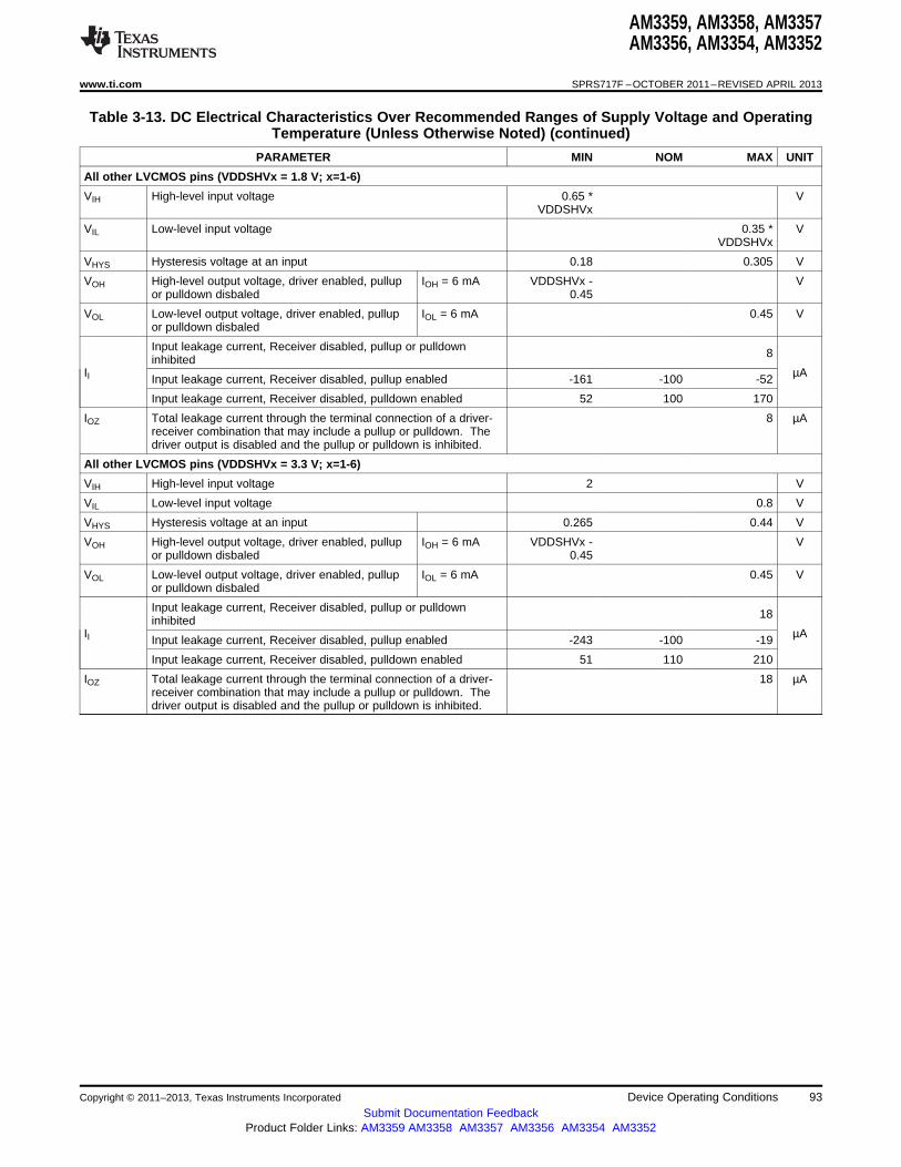
AM3359, AM3358, AM3357AM3356, AM3354, AM3352
www.ti.com SPRS717F –OCTOBER 2011–REVISED APRIL 2013
Table 3-13. DC Electrical Characteristics Over Recommended Ranges of Supply Voltage and OperatingTemperature (Unless Otherwise Noted) (continued)
PARAMETER MIN NOM MAX UNIT
All other LVCMOS pins (VDDSHVx = 1.8 V; x=1-6)
VIH High-level input voltage 0.65 * VVDDSHVx
VIL Low-level input voltage 0.35 * VVDDSHVx
VHYS Hysteresis voltage at an input 0.18 0.305 V
VOH High-level output voltage, driver enabled, pullup IOH = 6 mA VDDSHVx - Vor pulldown disbaled 0.45
VOL Low-level output voltage, driver enabled, pullup IOL = 6 mA 0.45 Vor pulldown disbaled
Input leakage current, Receiver disabled, pullup or pulldown 8inhibitedII µAInput leakage current, Receiver disabled, pullup enabled -161 -100 -52
Input leakage current, Receiver disabled, pulldown enabled 52 100 170
IOZ Total leakage current through the terminal connection of a driver- 8 µAreceiver combination that may include a pullup or pulldown. Thedriver output is disabled and the pullup or pulldown is inhibited.
All other LVCMOS pins (VDDSHVx = 3.3 V; x=1-6)
VIH High-level input voltage 2 V
VIL Low-level input voltage 0.8 V
VHYS Hysteresis voltage at an input 0.265 0.44 V
VOH High-level output voltage, driver enabled, pullup IOH = 6 mA VDDSHVx - Vor pulldown disbaled 0.45
VOL Low-level output voltage, driver enabled, pullup IOL = 6 mA 0.45 Vor pulldown disbaled
Input leakage current, Receiver disabled, pullup or pulldown 18inhibitedII µAInput leakage current, Receiver disabled, pullup enabled -243 -100 -19
Input leakage current, Receiver disabled, pulldown enabled 51 110 210
IOZ Total leakage current through the terminal connection of a driver- 18 µAreceiver combination that may include a pullup or pulldown. Thedriver output is disabled and the pullup or pulldown is inhibited.
Copyright © 2011–2013, Texas Instruments Incorporated Device Operating Conditions 93Submit Documentation Feedback
Product Folder Links: AM3359 AM3358 AM3357 AM3356 AM3354 AM3352
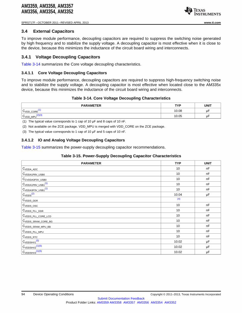
AM3359, AM3358, AM3357AM3356, AM3354, AM3352
SPRS717F –OCTOBER 2011–REVISED APRIL 2013 www.ti.com
3.4 External Capacitors
To improve module performance, decoupling capacitors are required to suppress the switching noise generatedby high frequency and to stabilize the supply voltage. A decoupling capacitor is most effective when it is close tothe device, because this minimizes the inductance of the circuit board wiring and interconnects.
3.4.1 Voltage Decoupling Capacitors
Table 3-14 summarizes the Core voltage decoupling characteristics.
3.4.1.1 Core Voltage Decoupling Capacitors
To improve module performance, decoupling capacitors are required to suppress high-frequency switching noiseand to stabilize the supply voltage. A decoupling capacitor is most effective when located close to the AM335xdevice, because this minimizes the inductance of the circuit board wiring and interconnects.
Table 3-14. Core Voltage Decoupling Characteristics
PARAMETER TYP UNIT
CVDD_CORE(1) 10.08 μF
CVDD_MPU(2)(3) 10.05 μF
(1) The typical value corresponds to 1 cap of 10 μF and 8 caps of 10 nF.
(2) Not available on the ZCE package. VDD_MPU is merged with VDD_CORE on the ZCE package.
(3) The typical value corresponds to 1 cap of 10 μF and 5 caps of 10 nF.
3.4.1.2 IO and Analog Voltage Decoupling Capacitors
Table 3-15 summarizes the power-supply decoupling capacitor recommendations.
Table 3-15. Power-Supply Decoupling Capacitor Characteristics
PARAMETER TYP UNIT
CVDDA_ADC 10 nF
CVDDA1P8V_USB0 10 nF
CCVDDA3P3V_USB0 10 nF
CVDDA1P8V_USB1(1) 10 nF
CVDDA3P3V_USB1(1) 10 nF
CVDDS(2) 10.04 μF
CVDDS_DDR(4)
CVDDS_OSC 10 nF
CVDDS_PLL_DDR 10 nF
CVDDS_PLL_CORE_LCD 10 nF
CVDDS_SRAM_CORE_BG 10 nF
CVDDS_SRAM_MPU_BB 10 nF
CVDDS_PLL_MPU 10 nF
CVDDS_RTC 10 nF
CVDDSHV1(5) 10.02 μF
CVDDSHV2(1)(5) 10.02 μF
CVDDSHV3(1)(5) 10.02 μF
94 Device Operating Conditions Copyright © 2011–2013, Texas Instruments Incorporated
Submit Documentation FeedbackProduct Folder Links: AM3359 AM3358 AM3357 AM3356 AM3354 AM3352
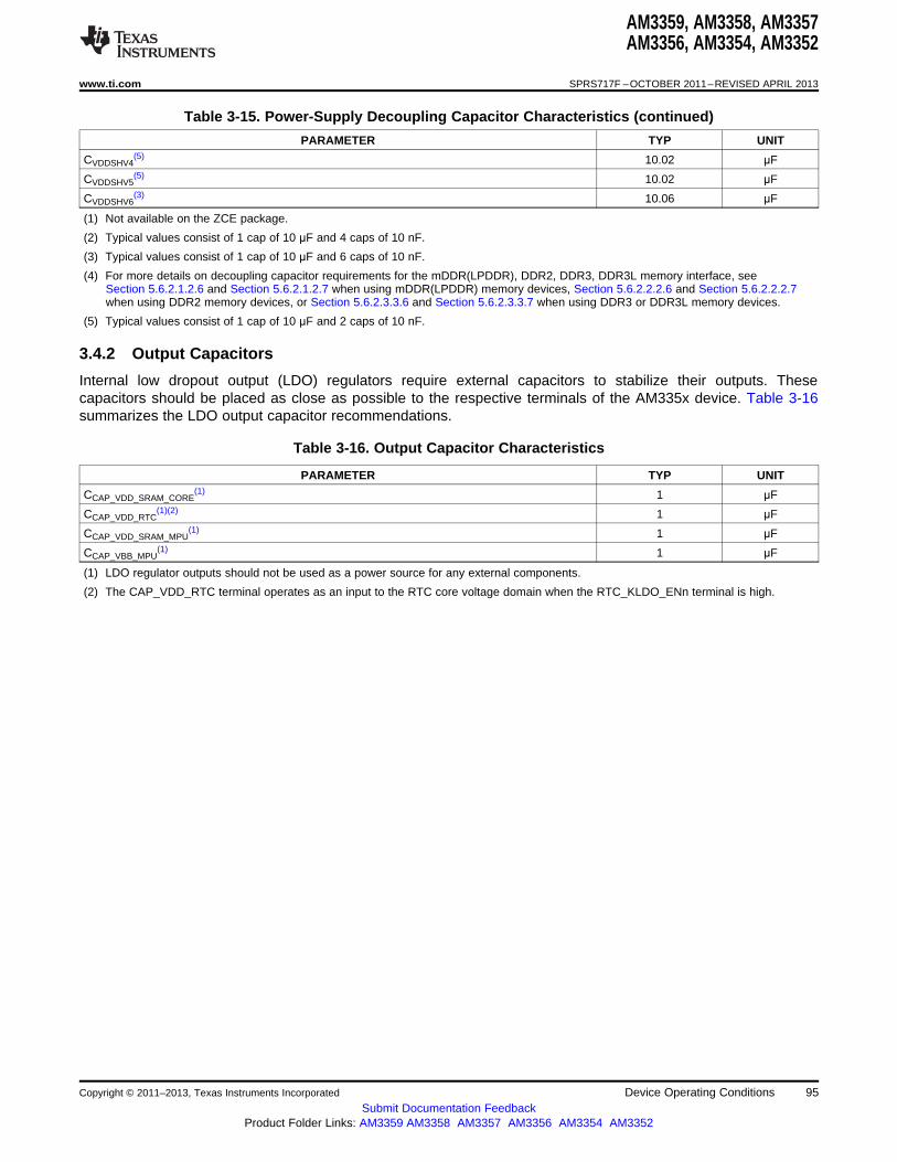
AM3359, AM3358, AM3357AM3356, AM3354, AM3352
www.ti.com SPRS717F –OCTOBER 2011–REVISED APRIL 2013
Table 3-15. Power-Supply Decoupling Capacitor Characteristics (continued)
PARAMETER TYP UNIT
CVDDSHV4(5) 10.02 μF
CVDDSHV5(5) 10.02 μF
CVDDSHV6(3) 10.06 μF
(1) Not available on the ZCE package.
(2) Typical values consist of 1 cap of 10 μF and 4 caps of 10 nF.
(3) Typical values consist of 1 cap of 10 μF and 6 caps of 10 nF.
(4) For more details on decoupling capacitor requirements for the mDDR(LPDDR), DDR2, DDR3, DDR3L memory interface, seeSection 5.6.2.1.2.6 and Section 5.6.2.1.2.7 when using mDDR(LPDDR) memory devices, Section 5.6.2.2.2.6 and Section 5.6.2.2.2.7when using DDR2 memory devices, or Section 5.6.2.3.3.6 and Section 5.6.2.3.3.7 when using DDR3 or DDR3L memory devices.
(5) Typical values consist of 1 cap of 10 μF and 2 caps of 10 nF.
3.4.2 Output Capacitors
Internal low dropout output (LDO) regulators require external capacitors to stabilize their outputs. Thesecapacitors should be placed as close as possible to the respective terminals of the AM335x device. Table 3-16summarizes the LDO output capacitor recommendations.
Table 3-16. Output Capacitor Characteristics
PARAMETER TYP UNIT
CCAP_VDD_SRAM_CORE(1) 1 μF
CCAP_VDD_RTC(1)(2) 1 μF
CCAP_VDD_SRAM_MPU(1) 1 μF
CCAP_VBB_MPU(1) 1 μF
(1) LDO regulator outputs should not be used as a power source for any external components.
(2) The CAP_VDD_RTC terminal operates as an input to the RTC core voltage domain when the RTC_KLDO_ENn terminal is high.
Copyright © 2011–2013, Texas Instruments Incorporated Device Operating Conditions 95Submit Documentation Feedback
Product Folder Links: AM3359 AM3358 AM3357 AM3356 AM3354 AM3352
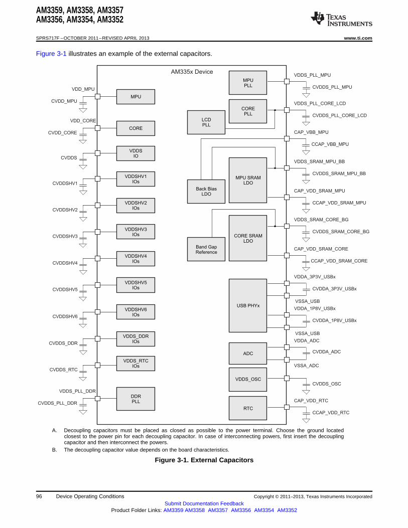
MPU
AM335x Device
VDD_MPU
CVDD_MPU
CORE
VDD_CORE
CVDD_CORE
VDDSIOCVDDS
VDDSHV2IOsCVDDSHV2
VDDSHV3IOsCVDDSHV3
VDDSHV4IOsCVDDSHV4
VDDSHV5IOsCVDDSHV5
VDDSHV6IOsCVDDSHV6
VDDS_DDRIOsCVDDS_DDR
VDDS_RTCIOs
CVDDS_RTC
DDRPLL
VDDS_PLL_DDR
CVDDS_PLL_DDR
MPUPLL
VDDS_PLL_MPU
CVDDS_PLL_MPU
COREPLL
VDDS_PLL_CORE_LCD
CVDDS_PLL_CORE_LCDLCDPLL
CAP_VBB_MPU
CCAP_VBB_MPU
MPU SRAMLDO
VDDS_SRAM_MPU_BB
CVDDS_SRAM_MPU_BB
CAP_VDD_SRAM_MPU
CCAP_VDD_SRAM_MPU
Back BiasLDO
CORE SRAMLDO
VDDS_SRAM_CORE_BG
CVDDS_SRAM_CORE_BG
CAP_VDD_SRAM_CORE
CCAP_VDD_SRAM_CORE
Band GapReference
USB PHYx
VDDA_3P3V_USBx
CVDDA_3P3V_USBx
VSSA_USB
VDDA_1P8V_USBx
CVDDA_1P8V_USBx
VSSA_USB
ADC
VDDA_ADC
CVDDA_ADC
VSSA_ADC
VDDS_OSCCVDDS_OSC
RTC
CAP_VDD_RTC
CCAP_VDD_RTC
VDDSHV1IOsCVDDSHV1
AM3359, AM3358, AM3357AM3356, AM3354, AM3352
SPRS717F –OCTOBER 2011–REVISED APRIL 2013 www.ti.com
Figure 3-1 illustrates an example of the external capacitors.
A. Decoupling capacitors must be placed as closed as possible to the power terminal. Choose the ground locatedclosest to the power pin for each decoupling capacitor. In case of interconnecting powers, first insert the decouplingcapacitor and then interconnect the powers.
B. The decoupling capacitor value depends on the board characteristics.
Figure 3-1. External Capacitors
96 Device Operating Conditions Copyright © 2011–2013, Texas Instruments Incorporated
Submit Documentation FeedbackProduct Folder Links: AM3359 AM3358 AM3357 AM3356 AM3354 AM3352
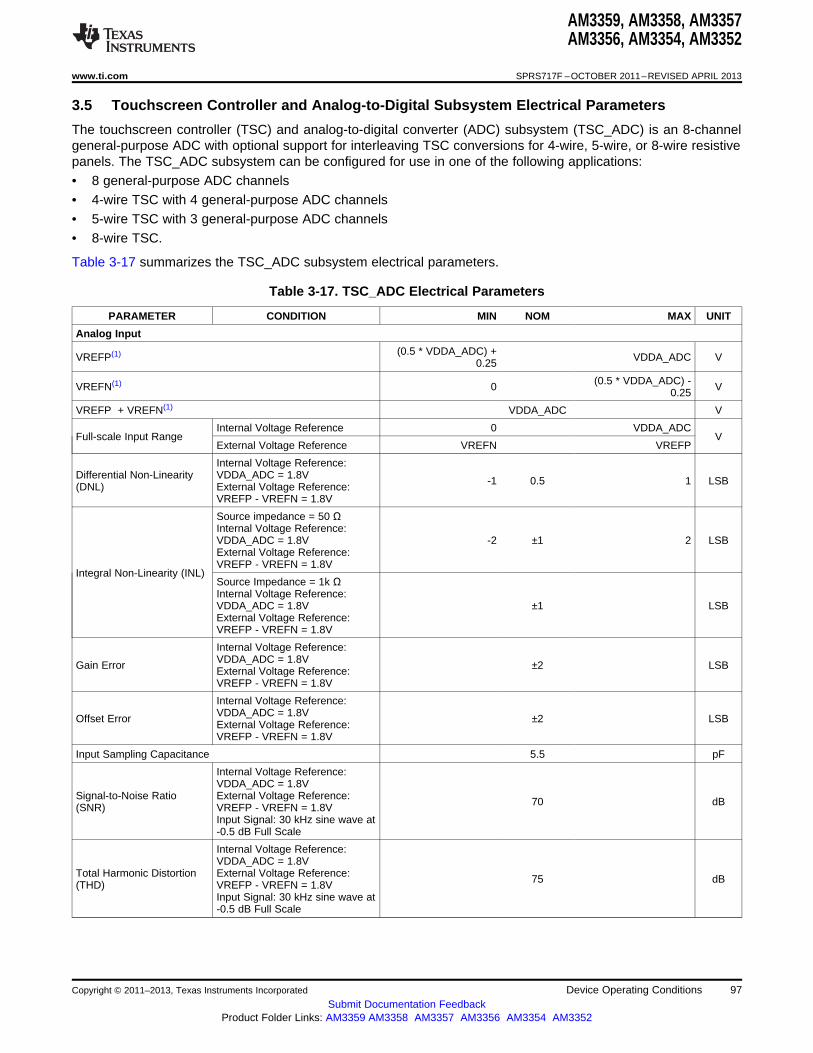
AM3359, AM3358, AM3357AM3356, AM3354, AM3352
www.ti.com SPRS717F –OCTOBER 2011–REVISED APRIL 2013
3.5 Touchscreen Controller and Analog-to-Digital Subsystem Electrical Parameters
The touchscreen controller (TSC) and analog-to-digital converter (ADC) subsystem (TSC_ADC) is an 8-channelgeneral-purpose ADC with optional support for interleaving TSC conversions for 4-wire, 5-wire, or 8-wire resistivepanels. The TSC_ADC subsystem can be configured for use in one of the following applications:• 8 general-purpose ADC channels• 4-wire TSC with 4 general-purpose ADC channels• 5-wire TSC with 3 general-purpose ADC channels• 8-wire TSC.
Table 3-17 summarizes the TSC_ADC subsystem electrical parameters.
Table 3-17. TSC_ADC Electrical Parameters
PARAMETER CONDITION MIN NOM MAX UNIT
Analog Input
(0.5 * VDDA_ADC) +VREFP(1) VDDA_ADC V0.25
(0.5 * VDDA_ADC) -VREFN(1) 0 V0.25
VREFP + VREFN(1) VDDA_ADC V
Internal Voltage Reference 0 VDDA_ADCFull-scale Input Range V
External Voltage Reference VREFN VREFP
Internal Voltage Reference:Differential Non-Linearity VDDA_ADC = 1.8V -1 0.5 1 LSB(DNL) External Voltage Reference:
VREFP - VREFN = 1.8V
Source impedance = 50 ΩInternal Voltage Reference:VDDA_ADC = 1.8V -2 ±1 2 LSBExternal Voltage Reference:VREFP - VREFN = 1.8V
Integral Non-Linearity (INL)Source Impedance = 1k ΩInternal Voltage Reference:VDDA_ADC = 1.8V ±1 LSBExternal Voltage Reference:VREFP - VREFN = 1.8V
Internal Voltage Reference:VDDA_ADC = 1.8VGain Error ±2 LSBExternal Voltage Reference:VREFP - VREFN = 1.8V
Internal Voltage Reference:VDDA_ADC = 1.8VOffset Error ±2 LSBExternal Voltage Reference:VREFP - VREFN = 1.8V
Input Sampling Capacitance 5.5 pF
Internal Voltage Reference:VDDA_ADC = 1.8V
Signal-to-Noise Ratio External Voltage Reference: 70 dB(SNR) VREFP - VREFN = 1.8VInput Signal: 30 kHz sine wave at-0.5 dB Full Scale
Internal Voltage Reference:VDDA_ADC = 1.8V
Total Harmonic Distortion External Voltage Reference: 75 dB(THD) VREFP - VREFN = 1.8VInput Signal: 30 kHz sine wave at-0.5 dB Full Scale
Copyright © 2011–2013, Texas Instruments Incorporated Device Operating Conditions 97Submit Documentation Feedback
Product Folder Links: AM3359 AM3358 AM3357 AM3356 AM3354 AM3352

AM3359, AM3358, AM3357AM3356, AM3354, AM3352
SPRS717F –OCTOBER 2011–REVISED APRIL 2013 www.ti.com
Table 3-17. TSC_ADC Electrical Parameters (continued)
PARAMETER CONDITION MIN NOM MAX UNIT
Internal Voltage Reference:VDDA_ADC = 1.8V
Spurious Free Dynamic External Voltage Reference: 80 dBRange VREFP - VREFN = 1.8VInput Signal: 30 kHz sine wave at-0.5 dB Full Scale
Internal Voltage Reference:VDDA_ADC = 1.8V
Signal-to-Noise Plus External Voltage Reference: 69 dBDistortion VREFP - VREFN = 1.8VInput Signal: 30 kHz sine wave at-0.5 dB Full Scale
VREFP and VREFN Input Impedance 20 kΩInput Impedance of f = input frequency [1/((65.97 x 10-12) x f)] ΩAIN[7:0](2)
Sampling Dynamics
ADCConversion Time 15 Clock
Cycles
ADCAcquisition Time 2 Clock
Cycles
Sampling Rate ADC Clock = 3 MHz 200 kSPS
Channel-to-Channel Isolation 100 dB
Touchscreen Switch Drivers
Pull-Up and Pull-Down Switch ON Resistance (Ron) 2 ΩPull-Up and Pull-DownSwitch Current Leakage Source impedance = 500 Ω 0.5 uAIleak
Drive Current 25 mA
Touchscreen Resistance 6 kΩPen Touch Detect 2 kΩ
(1) VREFP and VREFN must be tied to ground if the internal voltage reference is used.
(2) This parameter is valid when the respective AIN terminal is configured to operate as a general-purpose ADC input.
98 Device Operating Conditions Copyright © 2011–2013, Texas Instruments Incorporated
Submit Documentation FeedbackProduct Folder Links: AM3359 AM3358 AM3357 AM3356 AM3354 AM3352
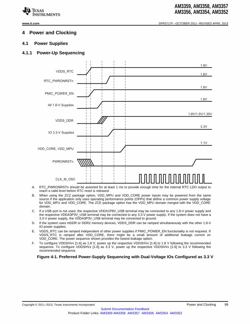
VDDS_RTC
RTC_PWRONRSTn
PMIC_POWER_EN
VDDS_DDR
All 1.8-V Supplies
IO 3.3-V Supplies
VDD_CORE, VDD_MPU
PWRONRSTn
CLK_M_OSC
1.8V
1.8V
1.8V
1.8V
1.8V/1.5V/1.35V
3.3V
1.1V
AM3359, AM3358, AM3357AM3356, AM3354, AM3352
www.ti.com SPRS717F –OCTOBER 2011–REVISED APRIL 2013
4 Power and Clocking
4.1 Power Supplies
4.1.1 Power-Up Sequencing
A. RTC_PWRONRSTn should be asserted for at least 1 ms to provide enough time for the internal RTC LDO output toreach a valid level before RTC reset is released.
B. When using the ZCZ package option, VDD_MPU and VDD_CORE power inputs may be powered from the samesource if the application only uses operating performance points (OPPs) that define a common power supply voltagefor VDD_MPU and VDD_CORE. The ZCE package option has the VDD_MPU domain merged with the VDD_COREdomain.
C. If a USB port is not used, the respective VDDA1P8V_USB terminal may be connected to any 1.8-V power supply andthe respective VDDA3P3V_USB terminal may be connected to any 3.3-V power supply. If the system does not have a3.3-V power supply, the VDDA3P3V_USB terminal may be connected to ground.
D. If the system uses mDDR or DDR2 memory devices, VDDS_DDR can be ramped simultaneously with the other 1.8-VIO power supplies.
E. VDDS_RTC can be ramped independent of other power supplies if PMIC_POWER_EN functionality is not required. IfVDDS_RTC is ramped after VDD_CORE, there might be a small amount of additional leakage current onVDD_CORE. The power sequence shown provides the lowest leakage option.
F. To configure VDDSHVx [1-6] as 1.8 V, power up the respective VDDSHVx [1-6] to 1.8 V following the recommendedsequence. To configure VDDSHVx [1-6] as 3.3 V, power up the respective VDDSHVx [1-6] to 3.3 V following therecommended sequence.
Figure 4-1. Preferred Power-Supply Sequencing with Dual-Voltage IOs Configured as 3.3 V
Copyright © 2011–2013, Texas Instruments Incorporated Power and Clocking 99Submit Documentation Feedback
Product Folder Links: AM3359 AM3358 AM3357 AM3356 AM3354 AM3352
See Notes Below
VDDS_RTC
RTC_PWRONRSTn
PMIC_POWER_EN
All 1.8-V SuppliesAll 3.3-V Supplies
VDDS_DDR
VDD_CORE, VDD_MPU
PWRONRSTn
CLK_M_OSC
1.8V
1.8V
1.8V
3.3V
1.8V
1.8V/1.5V/1.35V
1.1V
AM3359, AM3358, AM3357AM3356, AM3354, AM3352
SPRS717F –OCTOBER 2011–REVISED APRIL 2013 www.ti.com
A. RTC_PWRONRSTn should be asserted for at least 1 ms to provide enough time for the internal RTC LDO output toreach a valid level before RTC reset is released.
B. The 3.3-V IO power supplies may be ramped simultaneously with the 1.8-V IO power supplies if the voltage sourcedby any 3.3-V power supplies does not exceed the voltage sourced by any 1.8-V power supply by more than 2 V.Serious reliability issues may occur if the system power supply design allows any 3.3-V IO power supplies to exceedany 1.8-V IO power supplies by more than 2 V.
C. When using the ZCZ package option, VDD_MPU and VDD_CORE power inputs may be powered from the samesource if the application only uses operating performance points (OPPs) that define a common power supply voltagefor VDD_MPU and VDD_CORE. The ZCE package option has the VDD_MPU domain merged with the VDD_COREdomain.
D. If a USB port is not used, the respective VDDA1P8V_USB terminal may be connected to any 1.8-V power supply andthe respective VDDA3P3V_USB terminal may be connected to any 3.3-V power supply. If the system does not have a3.3-V power supply, the VDDA3P3V_USB terminal may be connected to ground.
E. If the system uses mDDR or DDR2 memory devices, VDDS_DDR can be ramped simultaneously with the other 1.8-VIO power supplies.
F. VDDS_RTC can be ramped independent of other power supplies if PMIC_POWER_EN functionality is not required. IfVDDS_RTC is ramped after VDD_CORE, there might be a small amount of additional leakage current onVDD_CORE. The power sequence shown provides the lowest leakage option.
G. To configure VDDSHVx [1-6] as 1.8 V, power up the respective VDDSHVx [1-6] to 1.8 V following the recommendedsequence. To configure VDDSHVx [1-6] as 3.3 V, power up the respective VDDSHVx [1-6] to 3.3 V following therecommended sequence.
Figure 4-2. Alternate Power-Supply Sequencing with Dual-Voltage IOs Configured as 3.3 V
100 Power and Clocking Copyright © 2011–2013, Texas Instruments Incorporated
Submit Documentation FeedbackProduct Folder Links: AM3359 AM3358 AM3357 AM3356 AM3354 AM3352

VDDS_RTC
RTC_PWRONRSTn
PMIC_POWER_EN
VDDS_DDR
All 1.8-V Supplies
All 3.3-V Supplies
VDD_CORE, VDD_MPU
PWRONRSTn
CLK_M_OSC
1.8V
1.8V
1.8V
1.8V
1.8V/1.5V/1.35V
3.3V
1.1V
AM3359, AM3358, AM3357AM3356, AM3354, AM3352
www.ti.com SPRS717F –OCTOBER 2011–REVISED APRIL 2013
A. RTC_PWRONRSTn should be asserted for at least 1 ms to provide enough time for the internal RTC LDO output toreach a valid level before RTC reset is released.
B. When using the ZCZ package option, VDD_MPU and VDD_CORE power inputs may be powered from the samesource if the application only uses operating performance points (OPPs) that define a common power supply voltagefor VDD_MPU and VDD_CORE. The ZCE package option has the VDD_MPU domain merged with the VDD_COREdomain.
C. If a USB port is not used, the respective VDDA1P8V_USB terminal may be connected to any 1.8-V power supply andthe respective VDDA3P3V_USB terminal may be connected to any 3.3-V power supply. If the system does not have a3.3-V power supply, the VDDA3P3V_USB terminal may be connected to ground.
D. If the system uses mDDR or DDR2 memory devices, VDDS_DDR can be ramped simultaneously with the other 1.8-VIO power supplies.
E. VDDS_RTC can be ramped independent of other power supplies if PMIC_POWER_EN functionality is not required. IfVDDS_RTC is ramped after VDD_CORE, there might be a small amount of additional leakage current onVDD_CORE. The power sequence shown provides the lowest leakage option.
F. To configure VDDSHVx [1-6] as 1.8 V, power up the respective VDDSHVx [1-6] to 1.8 V following the recommendedsequence. To configure VDDSHVx [1-6] as 3.3 V, power up the respective VDDSHVx [1-6] to 3.3 V following therecommended sequence.
Figure 4-3. Power-Supply Sequencing with Dual-Voltage IOs Configured as 1.8 V
Copyright © 2011–2013, Texas Instruments Incorporated Power and Clocking 101Submit Documentation Feedback
Product Folder Links: AM3359 AM3358 AM3357 AM3356 AM3354 AM3352

VDDS_RTC,CAP_VDD_RTC
RTC_PWRONRSTn
PMIC_POWER_EN
All other 1.8-V Supplies
VDDSHV 1-6
VDDS_DDR
All 3.3-V Supplies
VDD_CORE, VDD_MPU
PWRONRSTn
CLK_M_OSC
1.8V1.1V
1.8V
1.8V
1.8V
1.8V/1.5V/1.35V
3.3V
1.1V
AM3359, AM3358, AM3357AM3356, AM3354, AM3352
SPRS717F –OCTOBER 2011–REVISED APRIL 2013 www.ti.com
A. RTC_PWRONRSTn should be asserted for at least 1 ms to provide enough time for the internal RTC LDO output toreach a valid level before RTC reset is released.
B. The CAP_VDD_RTC terminal operates as an input to the RTC core voltage domain when the internal RTC LDO isdisabled by connecting the RTC_KALDO_ENn terminal to VDDS_RTC. If the internal RTC LDO is disabled,CAP_VDD_RTC should be sourced from an external 1.1-V power supply.
C. When using the ZCZ package option, VDD_MPU and VDD_CORE power inputs may be powered from the samesource if the application only uses operating performance points (OPPs) that define a common power supply voltagefor VDD_MPU and VDD_CORE. The ZCE package option has the VDD_MPU domain merged with the VDD_COREdomain.
D. If a USB port is not used, the respective VDDA1P8V_USB terminal may be connected to any 1.8-V power supply andthe respective VDDA3P3V_USB terminal may be connected to any 3.3-V power supply. If the system does not have a3.3-V power supply, the VDDA3P3V_USB terminal may be connected to ground.
E. If the system uses mDDR or DDR2 memory devices, VDDS_DDR can be ramped simultaneously with the other 1.8-VIO power supplies.
F. VDDS_RTC should be ramped at the same time or before CAP_VDD_RTC, but these power inputs can be rampedindependent of other power supplies if PMIC_POWER_EN functionality is not required. If CAP_VDD_RTC is rampedafter VDD_CORE, there might be a small amount of additional leakage current on VDD_CORE. The power sequenceshown provides the lowest leakage option.
G. To configure VDDSHVx [1-6] as 1.8 V, power up the respective VDDSHVx [1-6] to 1.8 V following the recommendedsequence. To configure VDDSHVx [1-6] as 3.3 V, power up the respective VDDSHVx [1-6] to 3.3 V following therecommended sequence.
Figure 4-4. Power-Supply Sequencing with Internal RTC LDO Disabled
102 Power and Clocking Copyright © 2011–2013, Texas Instruments Incorporated
Submit Documentation FeedbackProduct Folder Links: AM3359 AM3358 AM3357 AM3356 AM3354 AM3352
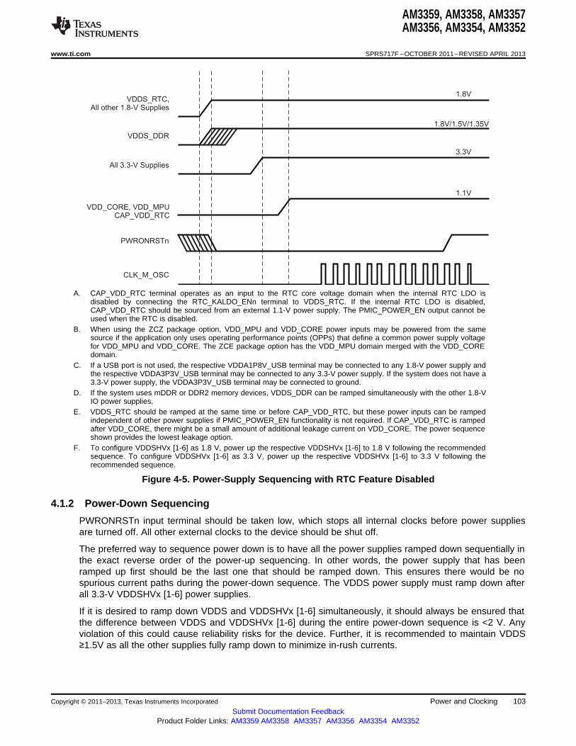
VDDS_RTC,All other 1.8-V Supplies
VDDS_DDR
All 3.3-V Supplies
VDD_CORE, VDD_MPUCAP_VDD_RTC
PWRONRSTn
CLK_M_OSC
1.8V
1.8V/1.5V/1.35V
3.3V
1.1V
AM3359, AM3358, AM3357AM3356, AM3354, AM3352
www.ti.com SPRS717F –OCTOBER 2011–REVISED APRIL 2013
A. CAP_VDD_RTC terminal operates as an input to the RTC core voltage domain when the internal RTC LDO isdisabled by connecting the RTC_KALDO_ENn terminal to VDDS_RTC. If the internal RTC LDO is disabled,CAP_VDD_RTC should be sourced from an external 1.1-V power supply. The PMIC_POWER_EN output cannot beused when the RTC is disabled.
B. When using the ZCZ package option, VDD_MPU and VDD_CORE power inputs may be powered from the samesource if the application only uses operating performance points (OPPs) that define a common power supply voltagefor VDD_MPU and VDD_CORE. The ZCE package option has the VDD_MPU domain merged with the VDD_COREdomain.
C. If a USB port is not used, the respective VDDA1P8V_USB terminal may be connected to any 1.8-V power supply andthe respective VDDA3P3V_USB terminal may be connected to any 3.3-V power supply. If the system does not have a3.3-V power supply, the VDDA3P3V_USB terminal may be connected to ground.
D. If the system uses mDDR or DDR2 memory devices, VDDS_DDR can be ramped simultaneously with the other 1.8-VIO power supplies.
E. VDDS_RTC should be ramped at the same time or before CAP_VDD_RTC, but these power inputs can be rampedindependent of other power supplies if PMIC_POWER_EN functionality is not required. If CAP_VDD_RTC is rampedafter VDD_CORE, there might be a small amount of additional leakage current on VDD_CORE. The power sequenceshown provides the lowest leakage option.
F. To configure VDDSHVx [1-6] as 1.8 V, power up the respective VDDSHVx [1-6] to 1.8 V following the recommendedsequence. To configure VDDSHVx [1-6] as 3.3 V, power up the respective VDDSHVx [1-6] to 3.3 V following therecommended sequence.
Figure 4-5. Power-Supply Sequencing with RTC Feature Disabled
4.1.2 Power-Down Sequencing
PWRONRSTn input terminal should be taken low, which stops all internal clocks before power suppliesare turned off. All other external clocks to the device should be shut off.
The preferred way to sequence power down is to have all the power supplies ramped down sequentially inthe exact reverse order of the power-up sequencing. In other words, the power supply that has beenramped up first should be the last one that should be ramped down. This ensures there would be nospurious current paths during the power-down sequence. The VDDS power supply must ramp down afterall 3.3-V VDDSHVx [1-6] power supplies.
If it is desired to ramp down VDDS and VDDSHVx [1-6] simultaneously, it should always be ensured thatthe difference between VDDS and VDDSHVx [1-6] during the entire power-down sequence is <2 V. Anyviolation of this could cause reliability risks for the device. Further, it is recommended to maintain VDDS≥1.5V as all the other supplies fully ramp down to minimize in-rush currents.
Copyright © 2011–2013, Texas Instruments Incorporated Power and Clocking 103Submit Documentation Feedback
Product Folder Links: AM3359 AM3358 AM3357 AM3356 AM3354 AM3352

AM335x Device
VDD_MPU
VDD_MPU_MON
Vfeedback
Connection for VDD_MPU_MON if voltage monitoring is used
Preferred connection for VDD_MPU_MON if voltage monitoring is NOT used
PowerManagement
IC
AM335x Device
VDD_MPU
VDD_MPU_MON PowerSource
Optional connection for VDD_MPU_MON if voltage monitoring is NOT used
AM335x Device
VDD_MPU
N/C
PowerSourceVDD_MPU_MON
AM3359, AM3358, AM3357AM3356, AM3354, AM3352
SPRS717F –OCTOBER 2011–REVISED APRIL 2013 www.ti.com
If none of the VDDSHVx [1-6] power supplies are configured as 3.3 V, the VDDS power supply may rampdown along with the VDDSHVx [1-6] supplies or after all the VDDSHVx [1-6] supplies have ramped down.It is recommended to maintain VDDS ≥1.5V as all the other supplies fully ramp down to minimize in-rushcurrents.
4.1.3 VDD_MPU_MON Connections
Figure 4-6 shows the VDD_MPU_MON connectivity. VDD_MPU_MON connectivity is available only on theZCZ package.
Figure 4-6. VDD_MPU_MON Connectivity
104 Power and Clocking Copyright © 2011–2013, Texas Instruments Incorporated
Submit Documentation FeedbackProduct Folder Links: AM3359 AM3358 AM3357 AM3356 AM3354 AM3352

MPUPLL
PERPLL
DDRPLL
COREPLL
LCDPLL
VDDS_PLL_MPU
VDDS_PLL_CORE_LCD
VDDA1P8V_USB0
VDDS_PLL_DDR
AM3359, AM3358, AM3357AM3356, AM3354, AM3352
www.ti.com SPRS717F –OCTOBER 2011–REVISED APRIL 2013
4.1.4 Digital Phase-Locked Loop Power Supply Requirements
The digital phase-locked loop (DPLL) provides all interface clocks and functional clocks to the processorof the AM335x device. The AM335x device integrates 5 different DPLLs—Core DPLL, Per DPLL, DisplayDPLL, DDR DPLL, MPU DPLL.
Figure 4-7 illustrates the power supply connectivity implemented in the AM335x device. Table 4-1 providesthe power supply requirements for the DPLL.
Figure 4-7. DPLL Power Supply Connectivity
Table 4-1. DPLL Power Supply Requirements
SUPPLY NAME DESCRIPTION MIN NOM MAX UNITS
VDDA1P8V_USB0 Supply voltage range for USBPHY and PER DPLL, Analog, 1.8V 1.71 1.8 1.89 V
Max. peak-to-peak supply noise 50 mV (p-p)
VDDS_PLL_MPU Supply voltage range for DPLL MPU, Analog 1.71 1.8 1.89 V
Max. peak-to-peak supply noise 50 mV (p-p)
VDDS_PLL_CORE_LCD Supply voltage range for DPLL CORE and LCD, Analog 1.71 1.8 1.89 V
Max. peak-to-peak supply noise 50 mV (p-p)
VDDS_PLL_DDR Supply voltage range for DPLL DDR, Analog 1.71 1.8 1.89 V
Max. peak-to-peak supply noise 50 mV (p-p)
Copyright © 2011–2013, Texas Instruments Incorporated Power and Clocking 105Submit Documentation Feedback
Product Folder Links: AM3359 AM3358 AM3357 AM3356 AM3354 AM3352

AM3359, AM3358, AM3357AM3356, AM3354, AM3352
SPRS717F –OCTOBER 2011–REVISED APRIL 2013 www.ti.com
4.2 Clock Specifications
4.2.1 Input Clock Specifications
The AM335x device has two clock inputs. Each clock input passes through an internal oscillator which canbe connected to an external crystal circuit (oscillator mode) or external LVCMOS square-wave digital clocksource (bypass mode). The oscillators automatically operate in bypass mode when their input isconnected to an external LVCMOS square-wave digital clock source. The oscillator associated with aspecific clock input must be enabled when the clock input is being used in either oscillator mode or bypassmode.
The OSC1 oscillator provides a 32.768-kHz reference clock to the real-time clock (RTC) and is connectedto the RTC_XTALIN and RTC_XTALOUT terminals. This clock source is referred to as the 32K oscillator(CLK_32K_RTC) in the AM335x ARM Cortex-A8 Microprocessors (MPUs) Technical Reference Manual(literature number SPRUH73). OSC1 is disabled by default after power is applied. This clock input isoptional and may not be required if the RTC is configured to receive a clock from the internal 32k RCoscillator (CLK_RC32K) or peripheral PLL (CLK_32KHZ) which receives a reference clock from the OSC0input.
The OSC0 oscillator provides a 19.2-MHz, 24-MHz, 25-MHz, or 26-MHz reference clock which is used toclock all non-RTC functions and is connected to the XTALIN and XTALOUT terminals. This clock source isreferred to as the master oscillator (CLK_M_OSC) in the AM335x ARM Cortex-A8 Microprocessors(MPUs) Technical Reference Manual (literature number SPRUH73). OSC0 is enabled by default afterpower is applied.
For more information related to recommended circuit topologies and crystal oscillator circuit requirementsfor these clock inputs, see Section 4.2.2.
4.2.2 Input Clock Requirements
4.2.2.1 OSC0 Internal Oscillator Clock Source
Figure 4-8 shows the recommended crystal circuit. It is recommended that pre-production printed circuitboard (PCB) designs include the two optional resistors Rbias and Rd in case they are required for properoscillator operation when combined with production crystal circuit components. In most cases, Rbias is notrequired and Rd is a 0-Ω resistor. These resistors may be removed from production PCB designs afterevaluating oscillator performance with production crystal circuit components installed on pre-productionPCBs.
The XTALIN terminal has a 15 - 40 kΩ internal pull-down resistor which is enabled when OSC0 isdisabled. This internal resistor prevents the XTALIN terminal from floating to an invalid logic level whichmay increase leakage current through the oscillator input buffer.
106 Power and Clocking Copyright © 2011–2013, Texas Instruments Incorporated
Submit Documentation FeedbackProduct Folder Links: AM3359 AM3358 AM3357 AM3356 AM3354 AM3352

AM335x
XTALIN VSS_OSC XTALOUT
C1
C2
Optional RdCrystal
Optional Rbias
AM3359, AM3358, AM3357AM3356, AM3354, AM3352
www.ti.com SPRS717F –OCTOBER 2011–REVISED APRIL 2013
A. Oscillator components (Crystal, C1, C2, optional Rbias and Rd) must be located close to the AM335x package.Parasitic capacitance to the printed circuit board (PCB) ground and other signals should be minimized to reduce noisecoupled into the oscillator. The VSS_OSC terminal provides a Kelvin ground reference for the external crystalcomponents. External crystal component grounds should only be connected to the VSS_OSC terminal and should notbe connected to the PCB ground plane.
B. C1 and C2 represent the total capacitance of the respective PCB trace, load capacitor, and other components(excluding the crystal) connected to each crystal terminal. The value of capacitors C1 and C2 should be selected toprovide the total load capacitance, CL, specified by the crystal manufacturer. The total load capacitance is CL =[(C1*C2)/(C1+C2)] + Cshunt, where Cshunt is the crystal shunt capacitance (C0) specified by the crystal manufacturerplus any mutual capacitance (Cpkg + CPCB) seen across the AM335x XTALIN and XTALOUT signals. Forrecommended values of crystal circuit components, see Table 4-2.
Figure 4-8. OSC0 Crystal Circuit Schematic
Table 4-2. OSC0 Crystal Circuit Requirements
NAME DESCRIPTION MIN TYP MAX UNIT
fxtal Crystal parallel resonance Fundamental mode oscillation only 19.2, 24.0, MHzfrequency 25.0, or
26.0
Crystal frequency stability -50.0 50.0 ppmand tolerance
CC1 C1 capacitance 12.0 24.0 pF
CC2 C2 capacitance 12.0 24.0 pF
Cshunt Shunt capacitance 5.0 pF
ESR Crystal effective series fxtal = 19.2 MHz, oscillator has nominal 54.4 Ωresistance negative resistance of 272 Ω and worst-
case negative resistance of 163 Ωfxtal = 24.0 MHz, oscillator has nominal 48.0 Ωnegative resistance of 240 Ω and worst-case negative resistance of 144 Ωfxtal = 25.0 MHz, oscillator has nominal 46.6 Ωnegative resistance of 233 Ω and worst-case negative resistance of 140 Ωfxtal = 26.0 MHz, oscillator has nominal 45.3 Ωnegative resistance of 227 Ω and worst-case negative resistance of 137 Ω
Copyright © 2011–2013, Texas Instruments Incorporated Power and Clocking 107Submit Documentation Feedback
Product Folder Links: AM3359 AM3358 AM3357 AM3356 AM3354 AM3352

VDDS_OSC
XTALOUT
tsX
VDD_CORE (min.)
Time
Voltage
VSS
VDDS_OSC (min.)
VSS
VDD_CORE
AM3359, AM3358, AM3357AM3356, AM3354, AM3352
SPRS717F –OCTOBER 2011–REVISED APRIL 2013 www.ti.com
Table 4-3. OSC0 Crystal Circuit Characteristics
NAME DESCRIPTION MIN TYP MAX UNIT
Cpkg Shunt capacitance of ZCE package 0.01 pFpackage ZCZ package 0.01 pF
Pxtal The actual values of the ESR, fxtal, and CL should be used to yield a Pxtal = 0.5 ESR (2 π fxtaltypical crystal power dissipation value. Using the maximum values CL VDDS_OSC)2
specified for ESR, fxtal, and CL parameters yields a maximum powerdissipation value.
tsX Start-up time 1.5 ms
Figure 4-9. OSC0 Start-up Time
108 Power and Clocking Copyright © 2011–2013, Texas Instruments Incorporated
Submit Documentation FeedbackProduct Folder Links: AM3359 AM3358 AM3357 AM3356 AM3354 AM3352
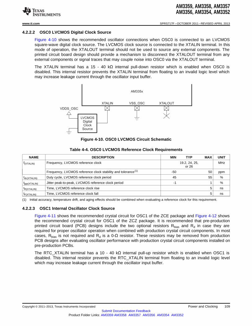
AM335x
XTALIN VSS_OSC XTALOUT
LVCMOSDigitalClock
Source
VDDS_OSC
AM3359, AM3358, AM3357AM3356, AM3354, AM3352
www.ti.com SPRS717F –OCTOBER 2011–REVISED APRIL 2013
4.2.2.2 OSC0 LVCMOS Digital Clock Source
Figure 4-10 shows the recommended oscillator connections when OSC0 is connected to an LVCMOSsquare-wave digital clock source. The LVCMOS clock source is connected to the XTALIN terminal. In thismode of operation, the XTALOUT terminal should not be used to source any external components. Theprinted circuit board design should provide a mechanism to disconnect the XTALOUT terminal from anyexternal components or signal traces that may couple noise into OSC0 via the XTALOUT terminal.
The XTALIN terminal has a 15 - 40 kΩ internal pull-down resistor which is enabled when OSC0 isdisabled. This internal resistor prevents the XTALIN terminal from floating to an invalid logic level whichmay increase leakage current through the oscillator input buffer.
Figure 4-10. OSC0 LVCMOS Circuit Schematic
Table 4-4. OSC0 LVCMOS Reference Clock Requirements
NAME DESCRIPTION MIN TYP MAX UNIT
f(XTALIN) Frequency, LVCMOS reference clock 19.2, 24, 25, MHzor 26
Frequency, LVCMOS reference clock stability and tolerance (1) -50 50 ppm
tdc(XTALIN) Duty cycle, LVCMOS reference clock period 45 55 %
tjpp(XTALIN) Jitter peak-to-peak, LVCMOS reference clock period -1 1 %
tR(XTALIN) Time, LVCMOS reference clock rise 5 ns
tF(XTALIN) Time, LVCMOS reference clock fall 5 ns
(1) Initial accuracy, temperature drift, and aging effects should be combined when evaluating a reference clock for this requirement.
4.2.2.3 OSC1 Internal Oscillator Clock Source
Figure 4-11 shows the recommended crystal circuit for OSC1 of the ZCE package and Figure 4-12 showsthe recommended crystal circuit for OSC1 of the ZCZ package. It is recommended that pre-productionprinted circuit board (PCB) designs include the two optional resistors Rbias and Rd in case they arerequired for proper oscillator operation when combined with production crystal circuit components. In mostcases, Rbias is not required and Rd is a 0-Ω resistor. These resistors may be removed from productionPCB designs after evaluating oscillator performance with production crystal circuit components installed onpre-production PCBs.
The RTC_XTALIN terminal has a 10 - 40 kΩ internal pull-up resistor which is enabled when OSC1 isdisabled. This internal resistor prevents the RTC_XTALIN terminal from floating to an invalid logic levelwhich may increase leakage current through the oscillator input buffer.
Copyright © 2011–2013, Texas Instruments Incorporated Power and Clocking 109Submit Documentation Feedback
Product Folder Links: AM3359 AM3358 AM3357 AM3356 AM3354 AM3352
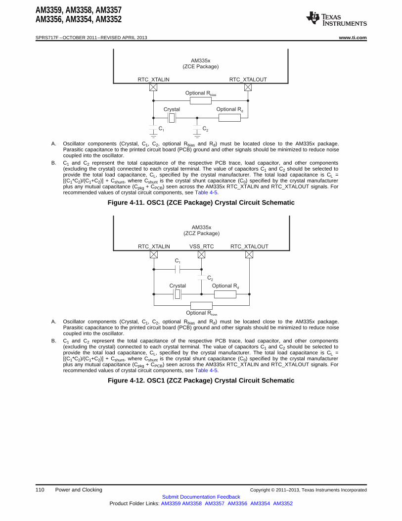
AM335x(ZCZ Package)
RTC_XTALIN VSS_RTC RTC_XTALOUT
C1
C2
Optional Rbias
Optional RdCrystal
AM335x(ZCE Package)
RTC_XTALIN RTC_XTALOUT
C1 C2
Optional Rbias
Optional RdCrystal
AM3359, AM3358, AM3357AM3356, AM3354, AM3352
SPRS717F –OCTOBER 2011–REVISED APRIL 2013 www.ti.com
A. Oscillator components (Crystal, C1, C2, optional Rbias and Rd) must be located close to the AM335x package.Parasitic capacitance to the printed circuit board (PCB) ground and other signals should be minimized to reduce noisecoupled into the oscillator.
B. C1 and C2 represent the total capacitance of the respective PCB trace, load capacitor, and other components(excluding the crystal) connected to each crystal terminal. The value of capacitors C1 and C2 should be selected toprovide the total load capacitance, CL, specified by the crystal manufacturer. The total load capacitance is CL =[(C1*C2)/(C1+C2)] + Cshunt, where Cshunt is the crystal shunt capacitance (C0) specified by the crystal manufacturerplus any mutual capacitance (Cpkg + CPCB) seen across the AM335x RTC_XTALIN and RTC_XTALOUT signals. Forrecommended values of crystal circuit components, see Table 4-5.
Figure 4-11. OSC1 (ZCE Package) Crystal Circuit Schematic
A. Oscillator components (Crystal, C1, C2, optional Rbias and Rd) must be located close to the AM335x package.Parasitic capacitance to the printed circuit board (PCB) ground and other signals should be minimized to reduce noisecoupled into the oscillator.
B. C1 and C2 represent the total capacitance of the respective PCB trace, load capacitor, and other components(excluding the crystal) connected to each crystal terminal. The value of capacitors C1 and C2 should be selected toprovide the total load capacitance, CL, specified by the crystal manufacturer. The total load capacitance is CL =[(C1*C2)/(C1+C2)] + Cshunt, where Cshunt is the crystal shunt capacitance (C0) specified by the crystal manufacturerplus any mutual capacitance (Cpkg + CPCB) seen across the AM335x RTC_XTALIN and RTC_XTALOUT signals. Forrecommended values of crystal circuit components, see Table 4-5.
Figure 4-12. OSC1 (ZCZ Package) Crystal Circuit Schematic
110 Power and Clocking Copyright © 2011–2013, Texas Instruments Incorporated
Submit Documentation FeedbackProduct Folder Links: AM3359 AM3358 AM3357 AM3356 AM3354 AM3352
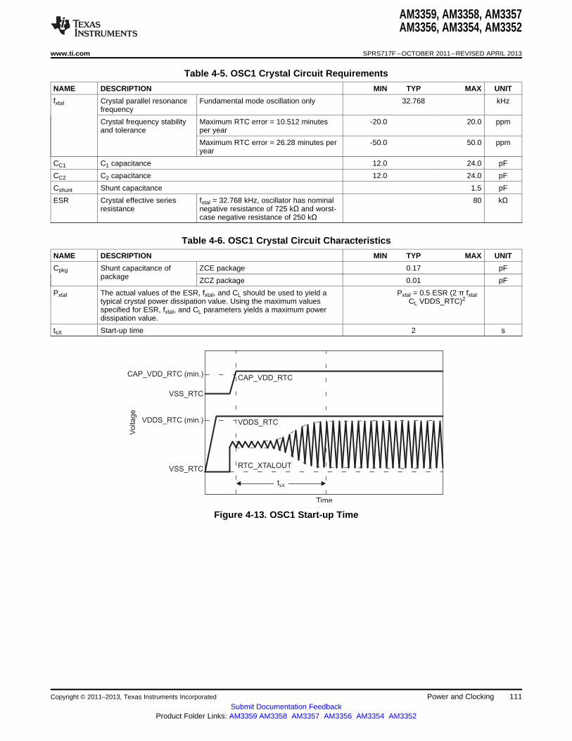
VDDS_RTC
RTC_XTALOUT
tsX
CAP_VDD_RTC (min.)
Time
Voltage
VSS_RTC
VDDS_RTC (min.)
VSS_RTC
CAP_VDD_RTC
AM3359, AM3358, AM3357AM3356, AM3354, AM3352
www.ti.com SPRS717F –OCTOBER 2011–REVISED APRIL 2013
Table 4-5. OSC1 Crystal Circuit Requirements
NAME DESCRIPTION MIN TYP MAX UNIT
fxtal Crystal parallel resonance Fundamental mode oscillation only 32.768 kHzfrequency
Crystal frequency stability Maximum RTC error = 10.512 minutes -20.0 20.0 ppmand tolerance per year
Maximum RTC error = 26.28 minutes per -50.0 50.0 ppmyear
CC1 C1 capacitance 12.0 24.0 pF
CC2 C2 capacitance 12.0 24.0 pF
Cshunt Shunt capacitance 1.5 pF
ESR Crystal effective series fxtal = 32.768 kHz, oscillator has nominal 80 kΩresistance negative resistance of 725 kΩ and worst-
case negative resistance of 250 kΩ
Table 4-6. OSC1 Crystal Circuit Characteristics
NAME DESCRIPTION MIN TYP MAX UNIT
Cpkg Shunt capacitance of ZCE package 0.17 pFpackage ZCZ package 0.01 pF
Pxtal The actual values of the ESR, fxtal, and CL should be used to yield a Pxtal = 0.5 ESR (2 π fxtaltypical crystal power dissipation value. Using the maximum values CL VDDS_RTC)2
specified for ESR, fxtal, and CL parameters yields a maximum powerdissipation value.
tsX Start-up time 2 s
Figure 4-13. OSC1 Start-up Time
Copyright © 2011–2013, Texas Instruments Incorporated Power and Clocking 111Submit Documentation Feedback
Product Folder Links: AM3359 AM3358 AM3357 AM3356 AM3354 AM3352
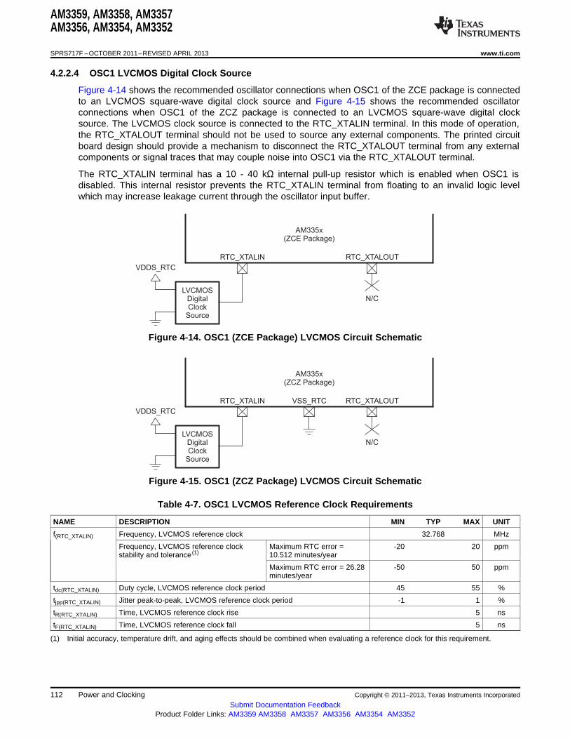
AM335x(ZCZ Package)
RTC_XTALIN RTC_XTALOUT
N/CLVCMOS
DigitalClock
Source
VSS_RTC
VDDS_RTC
AM335x(ZCE Package)
RTC_XTALIN RTC_XTALOUT
N/CLVCMOS
DigitalClock
Source
VDDS_RTC
AM3359, AM3358, AM3357AM3356, AM3354, AM3352
SPRS717F –OCTOBER 2011–REVISED APRIL 2013 www.ti.com
4.2.2.4 OSC1 LVCMOS Digital Clock Source
Figure 4-14 shows the recommended oscillator connections when OSC1 of the ZCE package is connectedto an LVCMOS square-wave digital clock source and Figure 4-15 shows the recommended oscillatorconnections when OSC1 of the ZCZ package is connected to an LVCMOS square-wave digital clocksource. The LVCMOS clock source is connected to the RTC_XTALIN terminal. In this mode of operation,the RTC_XTALOUT terminal should not be used to source any external components. The printed circuitboard design should provide a mechanism to disconnect the RTC_XTALOUT terminal from any externalcomponents or signal traces that may couple noise into OSC1 via the RTC_XTALOUT terminal.
The RTC_XTALIN terminal has a 10 - 40 kΩ internal pull-up resistor which is enabled when OSC1 isdisabled. This internal resistor prevents the RTC_XTALIN terminal from floating to an invalid logic levelwhich may increase leakage current through the oscillator input buffer.
Figure 4-14. OSC1 (ZCE Package) LVCMOS Circuit Schematic
Figure 4-15. OSC1 (ZCZ Package) LVCMOS Circuit Schematic
Table 4-7. OSC1 LVCMOS Reference Clock Requirements
NAME DESCRIPTION MIN TYP MAX UNIT
f(RTC_XTALIN) Frequency, LVCMOS reference clock 32.768 MHz
Frequency, LVCMOS reference clock Maximum RTC error = -20 20 ppmstability and tolerance (1) 10.512 minutes/year
Maximum RTC error = 26.28 -50 50 ppmminutes/year
tdc(RTC_XTALIN) Duty cycle, LVCMOS reference clock period 45 55 %
tjpp(RTC_XTALIN) Jitter peak-to-peak, LVCMOS reference clock period -1 1 %
tR(RTC_XTALIN) Time, LVCMOS reference clock rise 5 ns
tF(RTC_XTALIN) Time, LVCMOS reference clock fall 5 ns
(1) Initial accuracy, temperature drift, and aging effects should be combined when evaluating a reference clock for this requirement.
112 Power and Clocking Copyright © 2011–2013, Texas Instruments Incorporated
Submit Documentation FeedbackProduct Folder Links: AM3359 AM3358 AM3357 AM3356 AM3354 AM3352
AM335x(ZCZ Package)
RTC_XTALIN RTC_XTALOUT
N/C
VSS_RTC
N/C
AM335x(ZCE Package)
RTC_XTALIN RTC_XTALOUT
N/CN/C
AM3359, AM3358, AM3357AM3356, AM3354, AM3352
www.ti.com SPRS717F –OCTOBER 2011–REVISED APRIL 2013
4.2.2.5 OSC1 Not Used
Figure 4-16 shows the recommended oscillator connections when OSC1 of the ZCE package is not usedand Figure 4-17 shows the recommended oscillator connections when OSC1 of the ZCZ package is notused. An internal 10 kΩ pull-up on the RTC_XTALIN terminal is turned on when OSC1 is disabled toprevent this input from floating to an invalid logic level which may increase leakage current through theoscillator input buffer. OSC1 is disabled by default after power is applied. Therefore, both RTC_XTALINand RTC_XTALOUT terminals should be a no connect (NC) when OSC1 is not used.
Figure 4-16. OSC1 (ZCE Package) Not Used Schematic
Figure 4-17. OSC1 (ZCZ Package) Not Used Schematic
Copyright © 2011–2013, Texas Instruments Incorporated Power and Clocking 113Submit Documentation Feedback
Product Folder Links: AM3359 AM3358 AM3357 AM3356 AM3354 AM3352
AM3359, AM3358, AM3357AM3356, AM3354, AM3352
SPRS717F –OCTOBER 2011–REVISED APRIL 2013 www.ti.com
4.2.3 Output Clock Specifications
The AM335x device has two clock output signals. The CLKOUT1 signal is always a replica of the OSC0input clock which is referred to as the master oscillator (CLK_M_OSC) in the AM335x ARM Cortex-A8Microprocessors (MPUs) Technical Reference Manual (literature number SPRUH73). The CLKOUT2signal can be configured to output the OSC1 input clock, which is referred to as the 32K oscillator(CLK_32K_RTC) in the AM335x ARM Cortex-A8 Microprocessors (MPUs) Technical Reference Manual(literature number SPRUH73), or four other internal clocks. For more information related to configuringthese clock output signals, see the CLKOUT Signals section of the AM335x ARM Cortex-A8Microprocessors (MPUs) Technical Reference Manual (literature number SPRUH73).
4.2.4 Output Clock Characteristics
NOTEThe AM335x CLKOUT1 and CLKOUT2 clock outputs should not be used as a synchronousclock for any of the peripheral interfaces because they were not timing closed to any othersignals. These clock outputs also were not designed to source any time critical externalcircuits that require a low jitter reference clock. The jitter performance of these outputs isunpredictable due to complex combinations of many system variables. For example,CLKOUT2 may be sourced from several PLLs with each PLL supporting many configurationsthat yield different jitter performance. There are also other unpredictable contributors to jitterperformance such as application specific noise or crosstalk into the clock circuits. Therefore,there are no plans to specify jitter performance for these outputs.
4.2.4.1 CLKOUT1
The CLKOUT1 signal can be output on the XDMA_EVENT_INTR0 terminal. This terminal connects to oneof seven internal signals via configurable multiplexers. The XDMA_EVENT_INTR0 multiplexer must beconfigured for Mode 3 to connect the CLKOUT1 signal to the XDMA_EVENT_INTR0 terminal.
The default reset configuration of the XDMA_EVENT_INTR0 multiplexer is selected by the logic levelapplied to the LCD_DATA5 terminal on the rising edge of PWRONRSTn. The XDMA_EVENT_INTR0multiplexer is configured to Mode 7 if the LCD_DATA5 terminal is low on the rising edge of PWRONRSTnor Mode 3 if the LCD_DATA5 terminal is high on the rising edge of PWRONRSTn. This allows theCLKOUT1 signal to be output on the XDMA_EVENT_INTR0 terminal without software intervention. In thismode, the output is held low while PWRONRSTn is active and begins to toggle after PWRONRSTn isreleased.
4.2.4.2 CLKOUT2
The CLKOUT2 signal can be output on the XDMA_EVENT_INTR1 terminal. This terminal connects to oneof seven internal signals via configurable multiplexers. The XDMA_EVENT_INTR1 multiplexer must beconfigured for Mode 3 to connect the CLKOUT2 signal to the XDMA_EVENT_INTR1 terminal.
The default reset configuration of the XDMA_EVENT_INTR1 multiplexer is always Mode 7. Software mustconfigure the XDMA_EVENT_INTR1 multiplexer to Mode 3 for the CLKOUT2 signal to be output on theXDMA_EVENT_INTR1 terminal.
114 Power and Clocking Copyright © 2011–2013, Texas Instruments Incorporated
Submit Documentation FeedbackProduct Folder Links: AM3359 AM3358 AM3357 AM3356 AM3354 AM3352

AM3359, AM3358, AM3357AM3356, AM3354, AM3352
www.ti.com SPRS717F –OCTOBER 2011–REVISED APRIL 2013
5 Peripheral Information and Timings
The AM335x device contains many peripheral interfaces. In order to reduce package size and loweroverall system cost while maintaining maximum functionality, many of the AM335x terminals can multiplexup to eight signal functions. Although there are many combinations of pin multiplexing that are possible,only a certain number of sets, called IO Sets, are valid due to timing limitations. These valid IO Sets werecarefully chosen to provide many possible application scenarios for the user.
Texas Instruments has developed a Windows-based application called Pin Mux Utility that helps a systemdesigner select the appropriate pin-multiplexing configuration for their AM335x-based product design. ThePin Mux Utility provides a way to select valid IO Sets of specific peripheral interfaces to ensure the pin-multiplexing configuration selected for a design only uses valid IO Sets supported by the AM335x device.
5.1 Parameter Information
The data provided in the following Timing Requirements and Switching Characteristics tables assumes thedevice is operating within the Recommended Operating Conditions defined in Section 3, unless otherwisenoted.
5.1.1 Timing Parameters and Board Routing Analysis
The timing parameter values specified in this data manual do not include delays by board routings. As agood board design practice, such delays must always be taken into account. Timing values may beadjusted by increasing or decreasing such delays. TI recommends utilizing the available IO bufferinformation specification (IBIS) models to analyze the timing characteristics correctly. If needed, externallogic hardware such as buffers may be used to compensate any timing differences.
The timing parameter values specified in this data manual assume the SLEWCTRL bit in each pad controlregister is configured for fast mode (0b).
For the mDDR(LPDDR), DDR2, DDR3, DDR3L memory interface, it is not necessary to use the IBISmodels to analyze timing characteristics. TI provides a PCB routing rules solution that describes therouting rules to ensure the mDDR(LPDDR), DDR2, DDR3, DDR3L memory interface timings are met.
5.2 Recommended Clock and Control Signal Transition Behavior
All clocks and control signals must transition between VIH and VIL (or between VIL and VIH) in a monotonicmanner.
Copyright © 2011–2013, Texas Instruments Incorporated Peripheral Information and Timings 115Submit Documentation Feedback
Product Folder Links: AM3359 AM3358 AM3357 AM3356 AM3354 AM3352

1
DCANx_RX
2
DCANx_TX
AM3359, AM3358, AM3357AM3356, AM3354, AM3352
SPRS717F –OCTOBER 2011–REVISED APRIL 2013 www.ti.com
5.3 Controller Area Network (CAN)
For more information, see the Controller Area Network (CAN) section of the AM335x ARM Cortex-A8Microprocessors (MPUs) Technical Reference Manual (literature number SPRUH73).
5.3.1 DCAN Electrical Data and Timing
Table 5-1. Timing Requirements for DCANx Receive(see Figure 5-1)
NO. MIN MAX UNIT
fbaud(baud) Maximum programmable baud rate 1 Mbps
1 tw(RX) Pulse duration, receive data bit H - 2(1) H + 2(1) ns
(1) H = period of baud rate, 1/programmed baud rate.
Table 5-2. Switching Characteristics for DCANx Transmit(see Figure 5-1)
NO. PARAMETER MIN MAX UNIT
fbaud(baud) Maximum programmable baud rate 1 Mbps
2 tw(TX) Pulse duration, transmit data bit H - 2(1) H + 2(1) ns
(1) H = period of baud rate, 1/programmed baud rate.
Figure 5-1. DCANx Timings
116 Peripheral Information and Timings Copyright © 2011–2013, Texas Instruments Incorporated
Submit Documentation FeedbackProduct Folder Links: AM3359 AM3358 AM3357 AM3356 AM3354 AM3352

TCLKIN
TIMER[x]
1
23
AM3359, AM3358, AM3357AM3356, AM3354, AM3352
www.ti.com SPRS717F –OCTOBER 2011–REVISED APRIL 2013
5.4 DMTimer
5.4.1 DMTimer Electrical Data and Timing
Table 5-3. Timing Requirements for DMTimer [1-7](see Figure 5-2)
NO. MIN MAX UNIT
1 tc(TCLKIN) Cycle time, TCLKIN 4P+1 (1) ns
(1) P = period of PICLKOCP (interface clock).
Table 5-4. Switching Characteristics for DMTimer [4-7](see Figure 5-2)
NO. PARAMETER MIN MAX UNIT
2 tw(TIMERxH) Pulse duration, high 4P-3 (1) ns
3 tw(TIMERxL) Pulse duration, low 4P-3 (1) ns
(1) P = period of PICLKTIMER (functional clock).
Figure 5-2. Timer Timing
Copyright © 2011–2013, Texas Instruments Incorporated Peripheral Information and Timings 117Submit Documentation Feedback
Product Folder Links: AM3359 AM3358 AM3357 AM3356 AM3354 AM3352

MDIO_CLK Output)
1
2
MDIO_DATA (Input)
AM3359, AM3358, AM3357AM3356, AM3354, AM3352
SPRS717F –OCTOBER 2011–REVISED APRIL 2013 www.ti.com
5.5 Ethernet Media Access Controller (EMAC) and Switch
5.5.1 Ethernet MAC and Switch Electrical Data and Timing
The Ethernet MAC and Switch implemented in the AM335x device supports GMII mode, but the AM335xdesign does not pin out 9 of the 24 GMII signals. This was done to reduce the total number of packageterminals. Therefore, the AM335x device does not support GMII mode. MII mode is supported with theremaining GMII signals.
The AM335x ARM Cortex-A8 Microprocessors (MPUs) Technical Reference Manual (literature numberSPRUH73) and this document may reference internal signal names when discussing peripheral input andoutput signals since many of the AM335x package terminals can be multiplexed to one of severalperipheral signals. For example, the AM335x terminal names for port 1 of the Ethernet MAC and switchhave been changed from GMII to MII to indicate their Mode 0 function, but the internal signal is namedGMII. However, documents that describe the Ethernet switch reference these signals by their internalsignal name. For a cross-reference of internal signal names to terminal names, see Table 2-7.
Operation of the Ethernet MAC and switch is not supported for OPP50.
Table 5-5. Ethernet MAC and Switch Timing Conditions
TIMING CONDITION PARAMETER MIN TYP MAX UNIT
Input Conditions
tR Input signal rise time 1(1) 5(1) ns
tF Input signal fall time 1(1) 5(1) ns
Output Condition
CLOAD Output load capacitance 3 30 pF
(1) Except when specified otherwise.
5.5.1.1 Ethernet MAC/Switch MDIO Electrical Data and Timing
Table 5-6. Timing Requirements for MDIO_DATA(see Figure 5-3)
NO. MIN TYP MAX UNIT
1 tsu(MDIO-MDC) Setup time, MDIO valid before MDC high 90 ns
2 th(MDIO-MDC) Hold time, MDIO valid from MDC high 0 ns
Figure 5-3. MDIO_DATA Timing - Input Mode
Table 5-7. Switching Characteristics for MDIO_CLK(see Figure 5-4)
NO. PARAMETER MIN TYP MAX UNIT
1 tc(MDC) Cycle time, MDC 400 ns
2 tw(MDCH) Pulse duration, MDC high 160 ns
3 tw(MDCL) Pulse duration, MDC low 160 ns
4 tt(MDC) Transition time, MDC 5 ns
118 Peripheral Information and Timings Copyright © 2011–2013, Texas Instruments Incorporated
Submit Documentation FeedbackProduct Folder Links: AM3359 AM3358 AM3357 AM3356 AM3354 AM3352
GMII[x]_RXCLK
2 3
1 4
4
1
MDIO_CLK (Output)
MDIO_DATA (Output)
MDIO_CLK
2 3
1 4
4
AM3359, AM3358, AM3357AM3356, AM3354, AM3352
www.ti.com SPRS717F –OCTOBER 2011–REVISED APRIL 2013
Figure 5-4. MDIO_CLK Timing
Table 5-8. Switching Characteristics for MDIO_DATA(see Figure 5-5)
NO. PARAMETER MIN TYP MAX UNIT
1 td(MDC-MDIO) Delay time, MDC high to MDIO valid 10 390 ns
Figure 5-5. MDIO_DATA Timing - Output Mode
5.5.1.2 Ethernet MAC and Switch MII Electrical Data and Timing
Table 5-9. Timing Requirements for GMII[x]_RXCLK - MII Mode(see Figure 5-6)
10 Mbps 100 MbpsNO. UNIT
MIN TYP MAX MIN TYP MAX
1 tc(RX_CLK) Cycle time, RX_CLK 399.96 400.04 39.996 40.004 ns
2 tw(RX_CLKH) Pulse Duration, RX_CLK high 140 260 14 26 ns
3 tw(RX_CLKL) Pulse Duration, RX_CLK low 140 260 14 26 ns
4 tt(RX_CLK) Transition time, RX_CLK 5 5 ns
Figure 5-6. GMII[x]_RXCLK Timing - MII Mode
Copyright © 2011–2013, Texas Instruments Incorporated Peripheral Information and Timings 119Submit Documentation Feedback
Product Folder Links: AM3359 AM3358 AM3357 AM3356 AM3354 AM3352
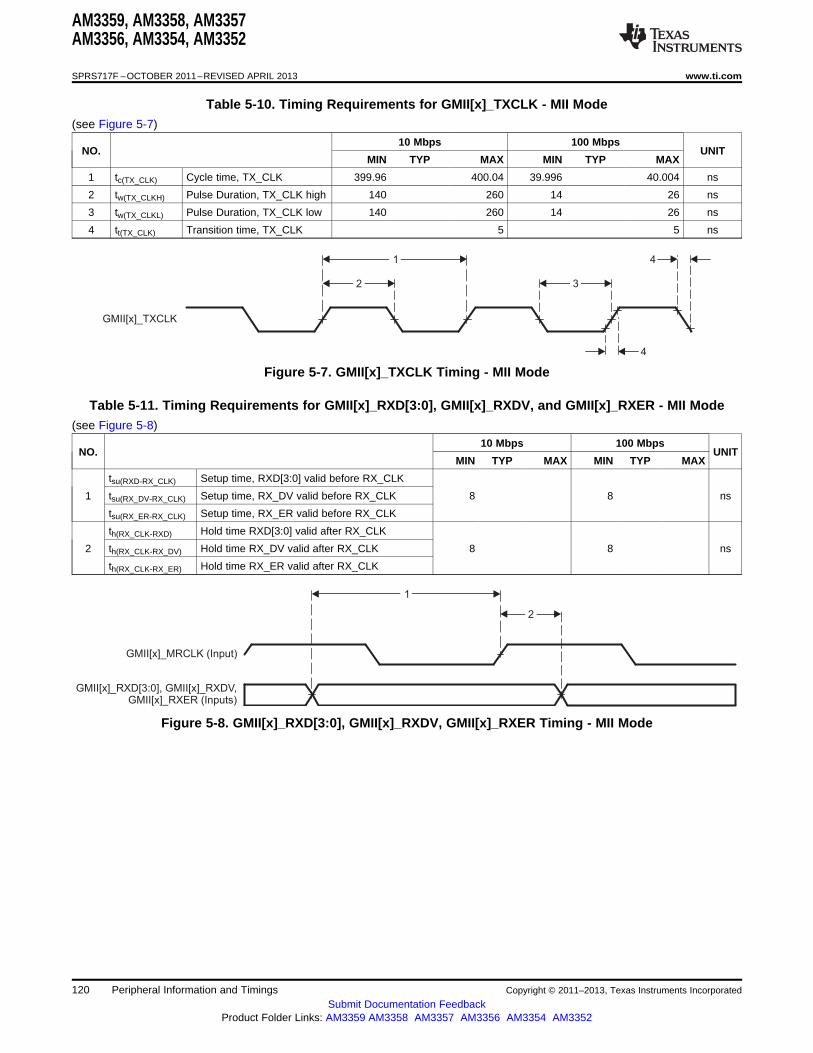
GMII[x]_MRCLK (Input)
1
2
GMII[x]_RXD[3:0], GMII[x]_RXDV,GMII[x]_RXER (Inputs)
GMII[x]_TXCLK
2 3
1 4
4
AM3359, AM3358, AM3357AM3356, AM3354, AM3352
SPRS717F –OCTOBER 2011–REVISED APRIL 2013 www.ti.com
Table 5-10. Timing Requirements for GMII[x]_TXCLK - MII Mode(see Figure 5-7)
10 Mbps 100 MbpsNO. UNIT
MIN TYP MAX MIN TYP MAX
1 tc(TX_CLK) Cycle time, TX_CLK 399.96 400.04 39.996 40.004 ns
2 tw(TX_CLKH) Pulse Duration, TX_CLK high 140 260 14 26 ns
3 tw(TX_CLKL) Pulse Duration, TX_CLK low 140 260 14 26 ns
4 tt(TX_CLK) Transition time, TX_CLK 5 5 ns
Figure 5-7. GMII[x]_TXCLK Timing - MII Mode
Table 5-11. Timing Requirements for GMII[x]_RXD[3:0], GMII[x]_RXDV, and GMII[x]_RXER - MII Mode(see Figure 5-8)
10 Mbps 100 MbpsNO. UNIT
MIN TYP MAX MIN TYP MAX
tsu(RXD-RX_CLK) Setup time, RXD[3:0] valid before RX_CLK
1 tsu(RX_DV-RX_CLK) Setup time, RX_DV valid before RX_CLK 8 8 ns
tsu(RX_ER-RX_CLK) Setup time, RX_ER valid before RX_CLK
th(RX_CLK-RXD) Hold time RXD[3:0] valid after RX_CLK
2 th(RX_CLK-RX_DV) Hold time RX_DV valid after RX_CLK 8 8 ns
th(RX_CLK-RX_ER) Hold time RX_ER valid after RX_CLK
Figure 5-8. GMII[x]_RXD[3:0], GMII[x]_RXDV, GMII[x]_RXER Timing - MII Mode
120 Peripheral Information and Timings Copyright © 2011–2013, Texas Instruments Incorporated
Submit Documentation FeedbackProduct Folder Links: AM3359 AM3358 AM3357 AM3356 AM3354 AM3352
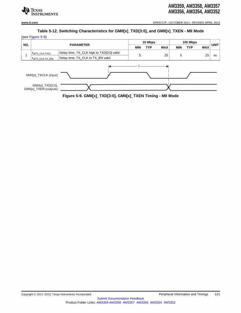
1
GMII[x]_TXCLK (input)
GMII[x]_TXD[3:0],GMII[x]_TXEN (outputs)
AM3359, AM3358, AM3357AM3356, AM3354, AM3352
www.ti.com SPRS717F –OCTOBER 2011–REVISED APRIL 2013
Table 5-12. Switching Characteristics for GMII[x]_TXD[3:0], and GMII[x]_TXEN - MII Mode(see Figure 5-9)
10 Mbps 100 MbpsNO. PARAMETER UNIT
MIN TYP MAX MIN TYP MAX
td(TX_CLK-TXD) Delay time, TX_CLK high to TXD[3:0] valid1 5 25 5 25 ns
td(TX_CLK-TX_EN) Delay time, TX_CLK to TX_EN valid
Figure 5-9. GMII[x]_TXD[3:0], GMII[x]_TXEN Timing - MII Mode
Copyright © 2011–2013, Texas Instruments Incorporated Peripheral Information and Timings 121Submit Documentation Feedback
Product Folder Links: AM3359 AM3358 AM3357 AM3356 AM3354 AM3352

RMII[x]_REFCLK (input)
1
2
RMII[x]_RXD[1:0], RMII[x]_CRS_DV,RMII[x]_RXER (inputs)
RMII[x]_REFCLK
(Input)
1
2
3
AM3359, AM3358, AM3357AM3356, AM3354, AM3352
SPRS717F –OCTOBER 2011–REVISED APRIL 2013 www.ti.com
5.5.1.3 Ethernet MAC and Switch RMII Electrical Data and Timing
Table 5-13. Timing Requirements for RMII[x]_REFCLK - RMII Mode(see Figure 5-10)
NO. MIN TYP MAX UNIT
1 tc(REF_CLK) Cycle time, REF_CLK 19.999 20.001 ns
2 tw(REF_CLKH) Pulse Duration, REF_CLK high 7 13 ns
3 tw(REF_CLKL) Pulse Duration, REF_CLK low 7 13 ns
Figure 5-10. RMII[x]_REFCLK Timing - RMII Mode
Table 5-14. Timing Requirements for RMII[x]_RXD[1:0], RMII[x]_CRS_DV, and RMII[x]_RXER - RMII Mode(see Figure 5-11)
NO. MIN TYP MAX UNIT
tsu(RXD-REF_CLK) Setup time, RXD[1:0] valid before REF_CLK
1 tsu(CRS_DV-REF_CLK) Setup time, CRS_DV valid before REF_CLK 4 ns
tsu(RX_ER-REF_CLK) Setup time, RX_ER valid before REF_CLK
th(REF_CLK-RXD) Hold time RXD[1:0] valid after REF_CLK
2 th(REF_CLK-CRS_DV) Hold time, CRS_DV valid after REF_CLK 2 ns
th(REF_CLK-RX_ER) Hold time, RX_ER valid after REF_CLK
Figure 5-11. RMII[x]_RXD[1:0], RMII[x]_CRS_DV, RMII[x]_RXER Timing - RMII Mode
122 Peripheral Information and Timings Copyright © 2011–2013, Texas Instruments Incorporated
Submit Documentation FeedbackProduct Folder Links: AM3359 AM3358 AM3357 AM3356 AM3354 AM3352
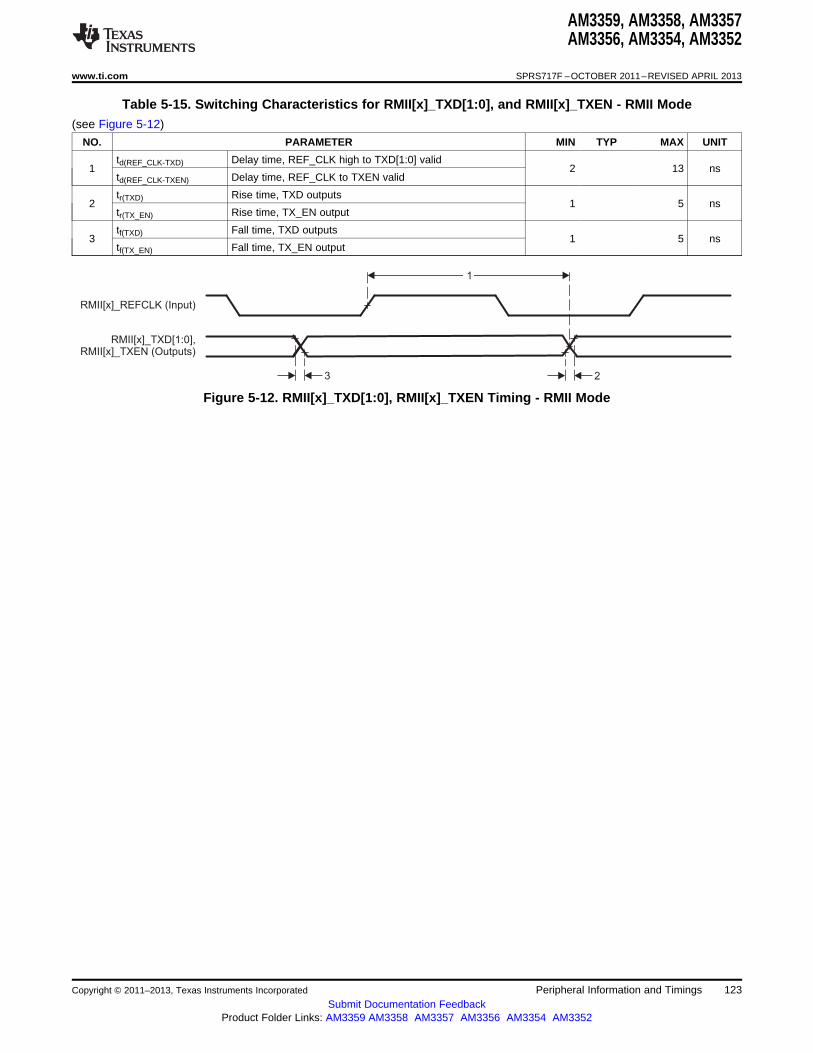
1
RMII[x]_REFCLK (Input)
RMII[x]_TXD[1:0],RMII[x]_TXEN (Outputs)
23
AM3359, AM3358, AM3357AM3356, AM3354, AM3352
www.ti.com SPRS717F –OCTOBER 2011–REVISED APRIL 2013
Table 5-15. Switching Characteristics for RMII[x]_TXD[1:0], and RMII[x]_TXEN - RMII Mode(see Figure 5-12)
NO. PARAMETER MIN TYP MAX UNIT
td(REF_CLK-TXD) Delay time, REF_CLK high to TXD[1:0] valid1 2 13 ns
td(REF_CLK-TXEN) Delay time, REF_CLK to TXEN valid
tr(TXD) Rise time, TXD outputs2 1 5 ns
tr(TX_EN) Rise time, TX_EN output
tf(TXD) Fall time, TXD outputs3 1 5 ns
tf(TX_EN) Fall time, TX_EN output
Figure 5-12. RMII[x]_TXD[1:0], RMII[x]_TXEN Timing - RMII Mode
Copyright © 2011–2013, Texas Instruments Incorporated Peripheral Information and Timings 123Submit Documentation Feedback
Product Folder Links: AM3359 AM3358 AM3357 AM3356 AM3354 AM3352

RGMII[x]_RD[3:0](B)
RGMII[x]_RCTL(B)
RGMII[x]_RCLK(A)
1
RXERR
1st Half-byte
2nd Half-byte2
3
RXDV
RGRXD[3:0] RGRXD[7:4]
RGMII[x]_RCLK
23
1
4
4
AM3359, AM3358, AM3357AM3356, AM3354, AM3352
SPRS717F –OCTOBER 2011–REVISED APRIL 2013 www.ti.com
5.5.1.4 Ethernet MAC and Switch RGMII Electrical Data and Timing
Table 5-16. Timing Requirements for RGMII[x]_RCLK - RGMII Mode(see Figure 5-13)
10 Mbps 100 Mbps 1000 MbpsNO. UNIT
MIN TYP MAX MIN TYP MAX MIN TYP MAX
1 tc(RXC) Cycle time, RXC 360 440 36 44 7.2 8.8 ns
Pulse duration, RXC2 tw(RXCH) 160 240 16 24 3.6 4.4 nshigh
3 tw(RXCL) Pulse duration, RXC low 160 240 16 24 3.6 4.4 ns
4 tt(RXC) Transition time, RXC 0.75 0.75 0.75 ns
Figure 5-13. RGMII[x]_RCLK Timing - RGMII Mode
Table 5-17. Timing Requirements for RGMII[x]_RD[3:0], and RGMII[x]_RCTL - RGMII Mode(see Figure 5-14)
10 Mbps 100 Mbps 1000 MbpsNO. UNIT
MIN TYP MAX MIN TYP MAX MIN TYP MAX
Setup time, RD[3:0] validtsu(RD-RXC) 1 1 1before RXC high or low1 ns
Setup time, RX_CTL validtsu(RX_CTL-RXC) 1 1 1before RXC high or low
Hold time, RD[3:0] validth(RXC-RD) 1 1 1after RXC high or low2 ns
Hold time, RX_CTL validth(RXC-RX_CTL) 1 1 1after RXC high or low
tt(RD) Transition time, RD 0.75 0.75 0.753 ns
tt(RX_CTL) Transition time, RX_CTL 0.75 0.75 0.75
A. RGMII[x]_RCLK must be externally delayed relative to the RGMII[x]_RD[3:0] and RGMII[x]_RCTL signals to meet therespective timing requirements.
B. Data and control information is received using both edges of the clocks. RGMII[x]_RD[3:0] carries data bits 3-0 on therising edge of RGMII[x]_RCLK and data bits 7-4 on the falling edge of RGMII[x]_RCLK. Similarly, RGMII[x]_RCTLcarries RXDV on rising edge of RGMII[x]_RCLK and RXERR on falling edge of RGMII[x]_RCLK.
Figure 5-14. RGMII[x]_RD[3:0], RGMII[x]_RCTL Timing - RGMII Mode
124 Peripheral Information and Timings Copyright © 2011–2013, Texas Instruments Incorporated
Submit Documentation FeedbackProduct Folder Links: AM3359 AM3358 AM3357 AM3356 AM3354 AM3352
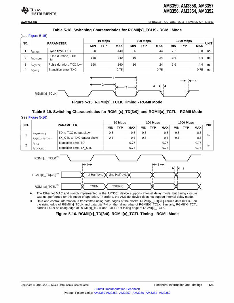
RGMII[x]_TCLK(A)
RGMII[x]_TD[3:0](B)
RGMII[x]_TCTL(B)
1
1st Half-byte
TXERRTXEN
2nd Half-byte
1
2
RGMII[x]_TCLK
4
4
23
1
AM3359, AM3358, AM3357AM3356, AM3354, AM3352
www.ti.com SPRS717F –OCTOBER 2011–REVISED APRIL 2013
Table 5-18. Switching Characteristics for RGMII[x]_TCLK - RGMII Mode(see Figure 5-15)
10 Mbps 100 Mbps 1000 MbpsNO. PARAMETER UNIT
MIN TYP MAX MIN TYP MAX MIN TYP MAX
1 tc(TXC) Cycle time, TXC 360 440 36 44 7.2 8.8 ns
Pulse duration, TXC2 tw(TXCH) 160 240 16 24 3.6 4.4 nshigh
3 tw(TXCL) Pulse duration, TXC low 160 240 16 24 3.6 4.4 ns
4 tt(TXC) Transition time, TXC 0.75 0.75 0.75 ns
Figure 5-15. RGMII[x]_TCLK Timing - RGMII Mode
Table 5-19. Switching Characteristics for RGMII[x]_TD[3:0], and RGMII[x]_TCTL - RGMII Mode(see Figure 5-16)
10 Mbps 100 Mbps 1000 MbpsNO. PARAMETER UNIT
MIN TYP MAX MIN TYP MAX MIN TYP MAX
tsk(TD-TXC) TD to TXC output skew -0.5 0.5 -0.5 0.5 -0.5 0.51 ns
tsk(TX_CTL-TXC) TX_CTL to TXC output skew -0.5 0.5 -0.5 0.5 -0.5 0.5
tt(TD) Transition time, TD 0.75 0.75 0.752 ns
tt(TX_CTL) Transition time, TX_CTL 0.75 0.75 0.75
A. The Ethernet MAC and switch implemented in the AM335x device supports internal delay mode, but timing closurewas not performed for this mode of operation. Therefore, the AM335x device does not support internal delay mode.
B. Data and control information is transmitted using both edges of the clocks. RGMII[x]_TD[3:0] carries data bits 3-0 onthe rising edge of RGMII[x]_TCLK and data bits 7-4 on the falling edge of RGMII[x]_TCLK. Similarly, RGMII[x]_TCTLcarries TXEN on rising edge of RGMII[x]_TCLK and TXERR of falling edge of RGMII[x]_TCLK.
Figure 5-16. RGMII[x]_TD[3:0], RGMII[x]_TCTL Timing - RGMII Mode
Copyright © 2011–2013, Texas Instruments Incorporated Peripheral Information and Timings 125Submit Documentation Feedback
Product Folder Links: AM3359 AM3358 AM3357 AM3356 AM3354 AM3352

AM3359, AM3358, AM3357AM3356, AM3354, AM3352
SPRS717F –OCTOBER 2011–REVISED APRIL 2013 www.ti.com
5.6 External Memory Interfaces
The device includes the following external memory interfaces:• General-purpose memory controller (GPMC)• mDDR(LPDDR), DDR2, DDR3, DDR3L Memory Interface (EMIF)
5.6.1 General-Purpose Memory Controller (GPMC)
NOTEFor more information, see the Memory Subsystem and General-Purpose Memory Controllersection of the AM335x ARM Cortex-A8 Microprocessors (MPUs) Technical ReferenceManual (literature number SPRUH73).
The GPMC is the unified memory controller used to interface external memory devices such as:• Asynchronous SRAM-like memories and ASIC devices• Asynchronous page mode and synchronous burst NOR flash• NAND flash
5.6.1.1 GPMC and NOR Flash—Synchronous Mode
Table 5-21 and Table 5-22 assume testing over the recommended operating conditions and electricalcharacteristic conditions below (see Figure 5-17 through Figure 5-21).
Table 5-20. GPMC and NOR Flash Timing Conditions—Synchronous Mode
TIMING CONDITION PARAMETER MIN TYP MAX UNIT
Input Conditions
tR Input signal rise time 1 5 ns
tF Input signal fall time 1 5 ns
Output Condition
CLOAD Output load capacitance 3 30 pF
Table 5-21. GPMC and NOR Flash Timing Requirements—Synchronous Mode
OPP100 OPP50NO. UNIT
MIN MAX MIN MAX
F12 tsu(dV-clkH) Setup time, input data gpmc_ad[15:0] valid before output clock 3.2 13.2 nsgpmc_clk high
F13 th(clkH-dV) Hold time, input data gpmc_ad[15:0] valid after output clock 4.74 2.75 nsgpmc_clk high
F21 tsu(waitV-clkH) Setup time, input wait gpmc_wait[x](1) valid before output clock 3.2 13.2 nsgpmc_clk high
F22 th(clkH-waitV) Hold time, input wait gpmc_wait[x](1) valid after output clock 4.74 2.75 nsgpmc_clk high
(1) In gpmc_wait[x], x is equal to 0 or 1.
126 Peripheral Information and Timings Copyright © 2011–2013, Texas Instruments Incorporated
Submit Documentation FeedbackProduct Folder Links: AM3359 AM3358 AM3357 AM3356 AM3354 AM3352

AM3359, AM3358, AM3357AM3356, AM3354, AM3352
www.ti.com SPRS717F –OCTOBER 2011–REVISED APRIL 2013
Table 5-22. GPMC and NOR Flash Switching Characteristics—Synchronous Mode(2)
OPP100 OPP50NO. PARAMETER UNIT
MIN MAX MIN MAX
F0 1 / tc(clk) Frequency(15), output clock gpmc_clk 100 50 MHz
F1 tw(clkH) Typical pulse duration, output clock gpmc_clk high 0.5P(12) 0.5P(12) 0.5P(12) 0.5P(12) ns
F1 tw(clkL) Typical pulse duration, output clock gpmc_clk low 0.5P(12) 0.5P(12) 0.5P(12) 0.5P(12) ns
tdc(clk) Duty cycle error, output clock gpmc_clk -500 500 -500 500 ps
tJ(clk) Jitter standard deviation(16), output clock gpmc_clk 33.33 33.33 ps
tR(clk) Rise time, output clock gpmc_clk 2 2 ns
tF(clk) Fall time, output clock gpmc_clk 2 2 ns
tR(do) Rise time, output data gpmc_ad[15:0] 2 2 ns
tF(do) Fall time, output data gpmc_ad[15:0] 2 2 ns
F2 td(clkH-csnV) Delay time, output clock gpmc_clk rising edge to F(6) - 2.2 F(6) + 4.5 F(6) - 3.2 F(6) + 9.5 nsoutput chip select gpmc_csn[x](11) transition
F3 td(clkH-csnIV) Delay time, output clock gpmc_clk rising edge to E(5) - 2.2 E(5) + 4.5 E(5) - 3.2 E(5) + 9.5 nsoutput chip select gpmc_csn[x](11) invalid
F4 td(aV-clk) Delay time, output address gpmc_a[27:1] valid to B(2) - 4.5 B(2) + 2.3 B(2) - 5.5 B(2) + 12.3 nsoutput clock gpmc_clk first edge
F5 td(clkH-aIV) Delay time, output clock gpmc_clk rising edge to -2.3 4.5 -3.3 14.5 nsoutput address gpmc_a[27:1] invalid
F6 td(be[x]nV-clk) Delay time, output lower byte enable and command B(2) - 1.9 B(2) + 2.3 B(2) - 2.9 B(2) + 12.3 nslatch enable gpmc_be0n_cle, output upper byteenable gpmc_be1n valid to output clock gpmc_clkfirst edge
F7 td(clkH-be[x]nIV) Delay time, output clock gpmc_clk rising edge to D(4) - 2.3 D(4) + 1.9 D(4) - 3.3 D(4) + 11.9 nsoutput lower byte enable and command latch enablegpmc_be0n_cle, output upper byte enablegpmc_be1n invalid
F8 td(clkH-advn) Delay time, output clock gpmc_clk rising edge to G(7) - 2.3 G(7) + 4.5 G(7) - 3.3 G(7) + 9.5 nsoutput address valid and address latch enablegpmc_advn_ale transition
F9 td(clkH-advnIV) Delay time, output clock gpmc_clk rising edge to D(4) - 2.3 D(4) + 3.5 D(4) - 3.3 D(4) + 9.5 nsoutput address valid and address latch enablegpmc_advn_ale invalid
F10 td(clkH-oen) Delay time, output clock gpmc_clk rising edge to H(8) - 2.3 H(8) + 3.5 H(8) - 3.3 H(8) + 8.5 nsoutput enable gpmc_oen transition
F11 td(clkH-oenIV) Delay time, output clock gpmc_clk rising edge to E(5) - 2.3 E(5) + 3.5 E(5) - 3.3 E(5) + 8.5 nsoutput enable gpmc_oen invalid
F14 td(clkH-wen) Delay time, output clock gpmc_clk rising edge to I(9) - 2.3 I(9) + 4.5 I(9) - 3.3 I(9) + 9.5 nsoutput write enable gpmc_wen transition
F15 td(clkH-do) Delay time, output clock gpmc_clk rising edge to J(10) - 2.3 J(10) + 1.9 J(10) - 3.3 J(10) + 11.9 nsoutput data gpmc_ad[15:0] transition
F17 td(clkH-be[x]n) Delay time, output clock gpmc_clk rising edge to J(10) - 2.3 J(10) + 1.9 J(10) - 3.3 J(10) + 11.9 nsoutput lower byte enable and command latch enablegpmc_be0n_cle transition
F18 tw(csnV) Pulse duration, output chip select Read A(1) A(1) nsgpmc_csn[x](11) low Write A(1) A(1) ns
F19 tw(be[x]nV) Pulse duration, output lower byte enable Read C(3) C(3) nsand command latch enable Write C(3) C(3) nsgpmc_be0n_cle, output upper byte enablegpmc_be1n low
F20 tw(advnV) Pulse duration, output address valid and Read K(13) K(13) nsaddress latch enable gpmc_advn_ale low Write K(13) K(13) ns
Copyright © 2011–2013, Texas Instruments Incorporated Peripheral Information and Timings 127Submit Documentation Feedback
Product Folder Links: AM3359 AM3358 AM3357 AM3356 AM3354 AM3352
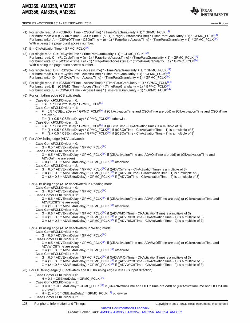
AM3359, AM3358, AM3357AM3356, AM3354, AM3352
SPRS717F –OCTOBER 2011–REVISED APRIL 2013 www.ti.com
(1) For single read: A = (CSRdOffTime - CSOnTime) * (TimeParaGranularity + 1) * GPMC_FCLK(14)
For burst read: A = (CSRdOffTime - CSOnTime + (n - 1) * PageBurstAccessTime) * (TimeParaGranularity + 1) * GPMC_FCLK(14)
For burst write: A = (CSWrOffTime - CSOnTime + (n - 1) * PageBurstAccessTime) * (TimeParaGranularity + 1) * GPMC_FCLK(14)
With n being the page burst access number.
(2) B = ClkActivationTime * GPMC_FCLK(14)
(3) For single read: C = RdCycleTime * (TimeParaGranularity + 1) * GPMC_FCLK (14)
For burst read: C = (RdCycleTime + (n - 1) * PageBurstAccessTime) * (TimeParaGranularity + 1) * GPMC_FCLK(14)
For burst write: C = (WrCycleTime + (n - 1) * PageBurstAccessTime) * (TimeParaGranularity + 1) * GPMC_FCLK(14)
With n being the page burst access number.
(4) For single read: D = (RdCycleTime - AccessTime) * (TimeParaGranularity + 1) * GPMC_FCLK(14)
For burst read: D = (RdCycleTime - AccessTime) * (TimeParaGranularity + 1) * GPMC_FCLK(14)
For burst write: D = (WrCycleTime - AccessTime) * (TimeParaGranularity + 1) * GPMC_FCLK(14)
(5) For single read: E = (CSRdOffTime - AccessTime) * (TimeParaGranularity + 1) * GPMC_FCLK(14)
For burst read: E = (CSRdOffTime - AccessTime) * (TimeParaGranularity + 1) * GPMC_FCLK(14)
For burst write: E = (CSWrOffTime - AccessTime) * (TimeParaGranularity + 1) * GPMC_FCLK(14)
(6) For csn falling edge (CS activated):
– Case GpmcFCLKDivider = 0:– F = 0.5 * CSExtraDelay * GPMC_FCLK(14)
– Case GpmcFCLKDivider = 1:– F = 0.5 * CSExtraDelay * GPMC_FCLK(14) if (ClkActivationTime and CSOnTime are odd) or (ClkActivationTime and CSOnTime
are even)– F = (1 + 0.5 * CSExtraDelay) * GPMC_FCLK(14) otherwise
– Case GpmcFCLKDivider = 2:– F = 0.5 * CSExtraDelay * GPMC_FCLK(14) if ((CSOnTime - ClkActivationTime) is a multiple of 3)– F = (1 + 0.5 * CSExtraDelay) * GPMC_FCLK(14) if ((CSOnTime - ClkActivationTime - 1) is a multiple of 3)– F = (2 + 0.5 * CSExtraDelay) * GPMC_FCLK(14) if ((CSOnTime - ClkActivationTime - 2) is a multiple of 3)
(7) For ADV falling edge (ADV activated):
– Case GpmcFCLKDivider = 0:– G = 0.5 * ADVExtraDelay * GPMC_FCLK(14)
– Case GpmcFCLKDivider = 1:– G = 0.5 * ADVExtraDelay * GPMC_FCLK(14) if (ClkActivationTime and ADVOnTime are odd) or (ClkActivationTime and
ADVOnTime are even)– G = (1 + 0.5 * ADVExtraDelay) * GPMC_FCLK(14) otherwise
– Case GpmcFCLKDivider = 2:– G = 0.5 * ADVExtraDelay * GPMC_FCLK(14) if ((ADVOnTime - ClkActivationTime) is a multiple of 3)– G = (1 + 0.5 * ADVExtraDelay) * GPMC_FCLK(14) if ((ADVOnTime - ClkActivationTime - 1) is a multiple of 3)– G = (2 + 0.5 * ADVExtraDelay) * GPMC_FCLK(14) if ((ADVOnTime - ClkActivationTime - 2) is a multiple of 3)
For ADV rising edge (ADV deactivated) in Reading mode:– Case GpmcFCLKDivider = 0:
– G = 0.5 * ADVExtraDelay * GPMC_FCLK(14)
– Case GpmcFCLKDivider = 1:– G = 0.5 * ADVExtraDelay * GPMC_FCLK(14) if (ClkActivationTime and ADVRdOffTime are odd) or (ClkActivationTime and
ADVRdOffTime are even)– G = (1 + 0.5 * ADVExtraDelay) * GPMC_FCLK(14) otherwise
– Case GpmcFCLKDivider = 2:– G = 0.5 * ADVExtraDelay * GPMC_FCLK(14) if ((ADVRdOffTime - ClkActivationTime) is a multiple of 3)– G = (1 + 0.5 * ADVExtraDelay) * GPMC_FCLK(14) if ((ADVRdOffTime - ClkActivationTime - 1) is a multiple of 3)– G = (2 + 0.5 * ADVExtraDelay) * GPMC_FCLK(14) if ((ADVRdOffTime - ClkActivationTime - 2) is a multiple of 3)
For ADV rising edge (ADV deactivated) in Writing mode:– Case GpmcFCLKDivider = 0:
– G = 0.5 * ADVExtraDelay * GPMC_FCLK(14)
– Case GpmcFCLKDivider = 1:– G = 0.5 * ADVExtraDelay * GPMC_FCLK(14) if (ClkActivationTime and ADVWrOffTime are odd) or (ClkActivationTime and
ADVWrOffTime are even)– G = (1 + 0.5 * ADVExtraDelay) * GPMC_FCLK(14) otherwise
– Case GpmcFCLKDivider = 2:– G = 0.5 * ADVExtraDelay * GPMC_FCLK(14) if ((ADVWrOffTime - ClkActivationTime) is a multiple of 3)– G = (1 + 0.5 * ADVExtraDelay) * GPMC_FCLK(14) if ((ADVWrOffTime - ClkActivationTime - 1) is a multiple of 3)– G = (2 + 0.5 * ADVExtraDelay) * GPMC_FCLK(14) if ((ADVWrOffTime - ClkActivationTime - 2) is a multiple of 3)
(8) For OE falling edge (OE activated) and IO DIR rising edge (Data Bus input direction):
– Case GpmcFCLKDivider = 0:– H = 0.5 * OEExtraDelay * GPMC_FCLK(14)
– Case GpmcFCLKDivider = 1:– H = 0.5 * OEExtraDelay * GPMC_FCLK(14) if (ClkActivationTime and OEOnTime are odd) or (ClkActivationTime and OEOnTime
are even)– H = (1 + 0.5 * OEExtraDelay) * GPMC_FCLK(14) otherwise
– Case GpmcFCLKDivider = 2:
128 Peripheral Information and Timings Copyright © 2011–2013, Texas Instruments Incorporated
Submit Documentation FeedbackProduct Folder Links: AM3359 AM3358 AM3357 AM3356 AM3354 AM3352
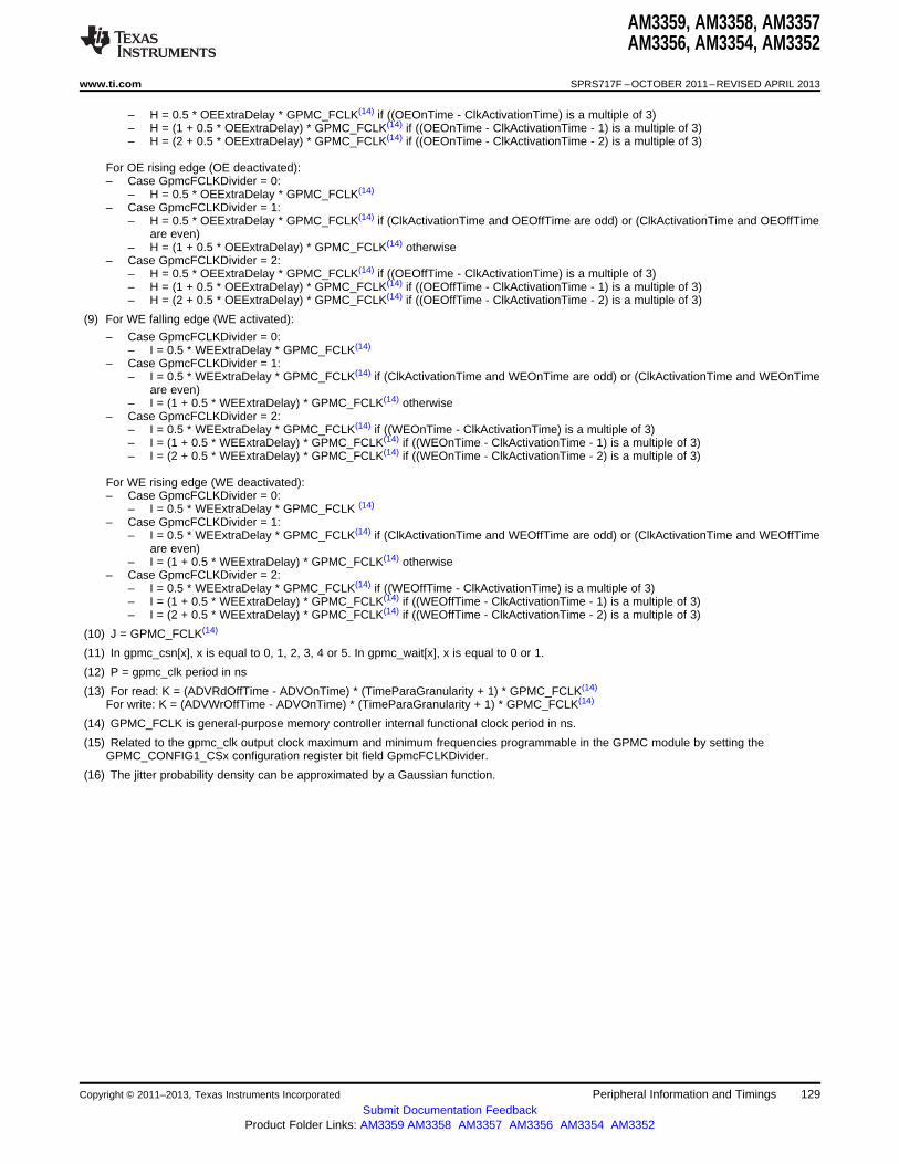
AM3359, AM3358, AM3357AM3356, AM3354, AM3352
www.ti.com SPRS717F –OCTOBER 2011–REVISED APRIL 2013
– H = 0.5 * OEExtraDelay * GPMC_FCLK(14) if ((OEOnTime - ClkActivationTime) is a multiple of 3)– H = (1 + 0.5 * OEExtraDelay) * GPMC_FCLK(14) if ((OEOnTime - ClkActivationTime - 1) is a multiple of 3)– H = (2 + 0.5 * OEExtraDelay) * GPMC_FCLK(14) if ((OEOnTime - ClkActivationTime - 2) is a multiple of 3)
For OE rising edge (OE deactivated):– Case GpmcFCLKDivider = 0:
– H = 0.5 * OEExtraDelay * GPMC_FCLK(14)
– Case GpmcFCLKDivider = 1:– H = 0.5 * OEExtraDelay * GPMC_FCLK(14) if (ClkActivationTime and OEOffTime are odd) or (ClkActivationTime and OEOffTime
are even)– H = (1 + 0.5 * OEExtraDelay) * GPMC_FCLK(14) otherwise
– Case GpmcFCLKDivider = 2:– H = 0.5 * OEExtraDelay * GPMC_FCLK(14) if ((OEOffTime - ClkActivationTime) is a multiple of 3)– H = (1 + 0.5 * OEExtraDelay) * GPMC_FCLK(14) if ((OEOffTime - ClkActivationTime - 1) is a multiple of 3)– H = (2 + 0.5 * OEExtraDelay) * GPMC_FCLK(14) if ((OEOffTime - ClkActivationTime - 2) is a multiple of 3)
(9) For WE falling edge (WE activated):
– Case GpmcFCLKDivider = 0:– I = 0.5 * WEExtraDelay * GPMC_FCLK(14)
– Case GpmcFCLKDivider = 1:– I = 0.5 * WEExtraDelay * GPMC_FCLK(14) if (ClkActivationTime and WEOnTime are odd) or (ClkActivationTime and WEOnTime
are even)– I = (1 + 0.5 * WEExtraDelay) * GPMC_FCLK(14) otherwise
– Case GpmcFCLKDivider = 2:– I = 0.5 * WEExtraDelay * GPMC_FCLK(14) if ((WEOnTime - ClkActivationTime) is a multiple of 3)– I = (1 + 0.5 * WEExtraDelay) * GPMC_FCLK(14) if ((WEOnTime - ClkActivationTime - 1) is a multiple of 3)– I = (2 + 0.5 * WEExtraDelay) * GPMC_FCLK(14) if ((WEOnTime - ClkActivationTime - 2) is a multiple of 3)
For WE rising edge (WE deactivated):– Case GpmcFCLKDivider = 0:
– I = 0.5 * WEExtraDelay * GPMC_FCLK (14)
– Case GpmcFCLKDivider = 1:– I = 0.5 * WEExtraDelay * GPMC_FCLK(14) if (ClkActivationTime and WEOffTime are odd) or (ClkActivationTime and WEOffTime
are even)– I = (1 + 0.5 * WEExtraDelay) * GPMC_FCLK(14) otherwise
– Case GpmcFCLKDivider = 2:– I = 0.5 * WEExtraDelay * GPMC_FCLK(14) if ((WEOffTime - ClkActivationTime) is a multiple of 3)– I = (1 + 0.5 * WEExtraDelay) * GPMC_FCLK(14) if ((WEOffTime - ClkActivationTime - 1) is a multiple of 3)– I = (2 + 0.5 * WEExtraDelay) * GPMC_FCLK(14) if ((WEOffTime - ClkActivationTime - 2) is a multiple of 3)
(10) J = GPMC_FCLK(14)
(11) In gpmc_csn[x], x is equal to 0, 1, 2, 3, 4 or 5. In gpmc_wait[x], x is equal to 0 or 1.
(12) P = gpmc_clk period in ns
(13) For read: K = (ADVRdOffTime - ADVOnTime) * (TimeParaGranularity + 1) * GPMC_FCLK(14)
For write: K = (ADVWrOffTime - ADVOnTime) * (TimeParaGranularity + 1) * GPMC_FCLK(14)
(14) GPMC_FCLK is general-purpose memory controller internal functional clock period in ns.
(15) Related to the gpmc_clk output clock maximum and minimum frequencies programmable in the GPMC module by setting theGPMC_CONFIG1_CSx configuration register bit field GpmcFCLKDivider.
(16) The jitter probability density can be approximated by a Gaussian function.
Copyright © 2011–2013, Texas Instruments Incorporated Peripheral Information and Timings 129Submit Documentation Feedback
Product Folder Links: AM3359 AM3358 AM3357 AM3356 AM3354 AM3352
gpmc_clk
gpmc_csn[x]
gpmc_a[10:1]
gpmc_be0n_cle
gpmc_be1n
gpmc_advn_ale
gpmc_oen
gpmc_ad[15:0]
gpmc_wait[x]
Valid Address
D 0
F0
F12
F13
F4
F6
F2
F8
F3
F7
F9
F11
F1
F1
F8
F19
F18
F20
F10
F6
F19
AM3359, AM3358, AM3357AM3356, AM3354, AM3352
SPRS717F –OCTOBER 2011–REVISED APRIL 2013 www.ti.com
A. In gpmc_csn[x], x is equal to 0, 1, 2, 3, 4 or 5.B. In gpmc_wait[x], x is equal to 0 or 1.
Figure 5-17. GPMC and NOR Flash—Synchronous Single Read—(GpmcFCLKDivider = 0)
130 Peripheral Information and Timings Copyright © 2011–2013, Texas Instruments Incorporated
Submit Documentation FeedbackProduct Folder Links: AM3359 AM3358 AM3357 AM3356 AM3354 AM3352

gpmc_clk
gpmc_csn[x]
gpmc_a[10:1]
gpmc_be0n_cle
gpmc_be1n
gpmc_advn_ale
gpmc_oen
gpmc_ad[15:0]
gpmc_wait[x]
Valid Address
D 0 D 1 D 2
F0
F12
F13 F13
F12
F4
F1
F1
F2
F6
F3
F7
F8 F8 F9
F10 F11
F21 F22
F6
F7
D 3
AM3359, AM3358, AM3357AM3356, AM3354, AM3352
www.ti.com SPRS717F –OCTOBER 2011–REVISED APRIL 2013
A. In gpmc_csn[x], x is equal to 0, 1, 2, 3, 4 or 5.B. In gpmc_wait[x], x is equal to 0 or 1.
Figure 5-18. GPMC and NOR Flash—Synchronous Burst Read—4x16-bit (GpmcFCLKDivider = 0)
Copyright © 2011–2013, Texas Instruments Incorporated Peripheral Information and Timings 131Submit Documentation Feedback
Product Folder Links: AM3359 AM3358 AM3357 AM3356 AM3354 AM3352
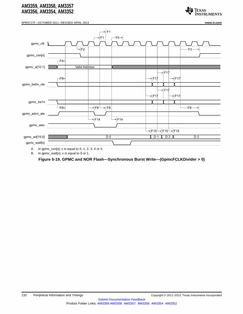
gpmc_clk
gpmc_csn[x]
gpmc_a[10:1]
gpmc_be0n_cle
gpmc_be1n
gpmc_advn_ale
gpmc_wen
gpmc_ad[15:0]
gpmc_wait[x]
D 0 D 1 D 2 D 3
F4
F15 F15 F15
F1
F1
F2
F6
F8F8
F0
F14F14
F3
F17
F17
F17
F9F6
F17
F17
F17
Valid Address
AM3359, AM3358, AM3357AM3356, AM3354, AM3352
SPRS717F –OCTOBER 2011–REVISED APRIL 2013 www.ti.com
A. In gpmc_csn[x], x is equal to 0, 1, 2, 3, 4 or 5.B. In gpmc_wait[x], x is equal to 0 or 1.
Figure 5-19. GPMC and NOR Flash—Synchronous Burst Write—(GpmcFCLKDivider > 0)
132 Peripheral Information and Timings Copyright © 2011–2013, Texas Instruments Incorporated
Submit Documentation FeedbackProduct Folder Links: AM3359 AM3358 AM3357 AM3356 AM3354 AM3352

gpmc_clk
gpmc_csn[x]
gpmc_be0n_cle
gpmc_be1n
gpmc_a[27:17]
gpmc_ad[15:0]
gpmc_advn_ale
gpmc_oen
gpmc_wait[x]
Valid
Valid
Address (MSB)
Address (LSB) D0 D1 D2 D3
F4
F6
F4
F2
F8 F8
F10
F13
F12
F12
F11
F9
F7
F3
F0 F1
F1
F5
F6 F7
AM3359, AM3358, AM3357AM3356, AM3354, AM3352
www.ti.com SPRS717F –OCTOBER 2011–REVISED APRIL 2013
A. In gpmc_csn[x], x is equal to 0, 1, 2, 3, 4 or 5.B. In gpmc_wait[x], x is equal to 0 or 1.
Figure 5-20. GPMC and Multiplexed NOR Flash—Synchronous Burst Read
Copyright © 2011–2013, Texas Instruments Incorporated Peripheral Information and Timings 133Submit Documentation Feedback
Product Folder Links: AM3359 AM3358 AM3357 AM3356 AM3354 AM3352
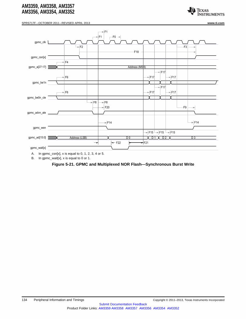
gpmc_clk
gpmc_csn[x]
gpmc_a[27:17]
gpmc_be1n
gpmc_be0n_cle
gpmc_advn_ale
gpmc_wen
gpmc_wait[x]
Address (LSB) D 0 D 1 D 2 D 3
F4
F15 F15 F15
F1
F1
F2
F6
F8F8
F0
F3
F17
F17
F17
F9
F6 F17
F17
F17
F18
F20
F14
F22 F21
Address (MSB)
gpmc_ad[15:0]
F14
AM3359, AM3358, AM3357AM3356, AM3354, AM3352
SPRS717F –OCTOBER 2011–REVISED APRIL 2013 www.ti.com
A. In gpmc_csn[x], x is equal to 0, 1, 2, 3, 4 or 5.B. In gpmc_wait[x], x is equal to 0 or 1.
Figure 5-21. GPMC and Multiplexed NOR Flash—Synchronous Burst Write
134 Peripheral Information and Timings Copyright © 2011–2013, Texas Instruments Incorporated
Submit Documentation FeedbackProduct Folder Links: AM3359 AM3358 AM3357 AM3356 AM3354 AM3352
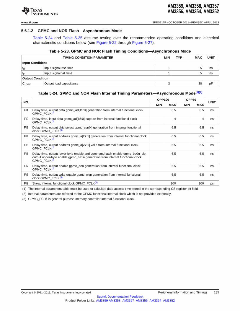
AM3359, AM3358, AM3357AM3356, AM3354, AM3352
www.ti.com SPRS717F –OCTOBER 2011–REVISED APRIL 2013
5.6.1.2 GPMC and NOR Flash—Asynchronous Mode
Table 5-24 and Table 5-25 assume testing over the recommended operating conditions and electricalcharacteristic conditions below (see Figure 5-22 through Figure 5-27).
Table 5-23. GPMC and NOR Flash Timing Conditions—Asynchronous Mode
TIMING CONDITION PARAMETER MIN TYP MAX UNIT
Input Conditions
tR Input signal rise time 1 5 ns
tF Input signal fall time 1 5 ns
Output Condition
CLOAD Output load capacitance 3 30 pF
Table 5-24. GPMC and NOR Flash Internal Timing Parameters—Asynchronous Mode(1)(2)
OPP100 OPP50NO. UNIT
MIN MAX MIN MAX
FI1 Delay time, output data gpmc_ad[15:0] generation from internal functional clock 6.5 6.5 nsGPMC_FCLK(3)
FI2 Delay time, input data gpmc_ad[15:0] capture from internal functional clock 4 4 nsGPMC_FCLK(3)
FI3 Delay time, output chip select gpmc_csn[x] generation from internal functional 6.5 6.5 nsclock GPMC_FCLK(3)
FI4 Delay time, output address gpmc_a[27:1] generation from internal functional clock 6.5 6.5 nsGPMC_FCLK(3)
FI5 Delay time, output address gpmc_a[27:1] valid from internal functional clock 6.5 6.5 nsGPMC_FCLK(3)
FI6 Delay time, output lower-byte enable and command latch enable gpmc_be0n_cle, 6.5 6.5 nsoutput upper-byte enable gpmc_be1n generation from internal functional clockGPMC_FCLK(3)
FI7 Delay time, output enable gpmc_oen generation from internal functional clock 6.5 6.5 nsGPMC_FCLK(3)
FI8 Delay time, output write enable gpmc_wen generation from internal functional 6.5 6.5 nsclock GPMC_FCLK(3)
FI9 Skew, internal functional clock GPMC_FCLK(3) 100 100 ps
(1) The internal parameters table must be used to calculate data access time stored in the corresponding CS register bit field.
(2) Internal parameters are referred to the GPMC functional internal clock which is not provided externally.
(3) GPMC_FCLK is general-purpose memory controller internal functional clock.
Copyright © 2011–2013, Texas Instruments Incorporated Peripheral Information and Timings 135Submit Documentation Feedback
Product Folder Links: AM3359 AM3358 AM3357 AM3356 AM3354 AM3352
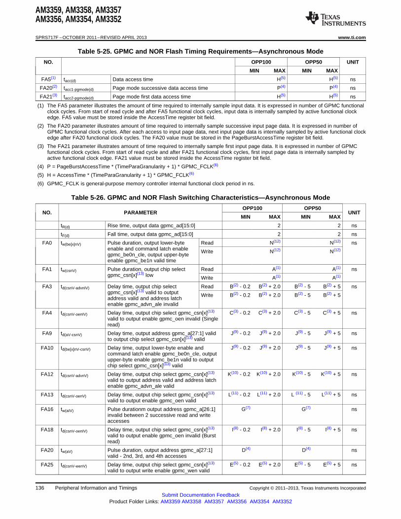
AM3359, AM3358, AM3357AM3356, AM3354, AM3352
SPRS717F –OCTOBER 2011–REVISED APRIL 2013 www.ti.com
Table 5-25. GPMC and NOR Flash Timing Requirements—Asynchronous Mode
NO. OPP100 OPP50 UNIT
MIN MAX MIN MAX
FA5(1) tacc(d) Data access time H(5) H(5) ns
FA20(2) tacc1-pgmode(d) Page mode successive data access time P(4) P(4) ns
FA21(3) tacc2-pgmode(d) Page mode first data access time H(5) H(5) ns
(1) The FA5 parameter illustrates the amount of time required to internally sample input data. It is expressed in number of GPMC functionalclock cycles. From start of read cycle and after FA5 functional clock cycles, input data is internally sampled by active functional clockedge. FA5 value must be stored inside the AccessTime register bit field.
(2) The FA20 parameter illustrates amount of time required to internally sample successive input page data. It is expressed in number ofGPMC functional clock cycles. After each access to input page data, next input page data is internally sampled by active functional clockedge after FA20 functional clock cycles. The FA20 value must be stored in the PageBurstAccessTime register bit field.
(3) The FA21 parameter illustrates amount of time required to internally sample first input page data. It is expressed in number of GPMCfunctional clock cycles. From start of read cycle and after FA21 functional clock cycles, first input page data is internally sampled byactive functional clock edge. FA21 value must be stored inside the AccessTime register bit field.
(4) P = PageBurstAccessTime * (TimeParaGranularity + 1) * GPMC_FCLK(6)
(5) H = AccessTime * (TimeParaGranularity + 1) * GPMC_FCLK(6)
(6) GPMC_FCLK is general-purpose memory controller internal functional clock period in ns.
Table 5-26. GPMC and NOR Flash Switching Characteristics—Asynchronous Mode
OPP100 OPP50NO. PARAMETER UNIT
MIN MAX MIN MAX
tR(d) Rise time, output data gpmc_ad[15:0] 2 2 ns
tF(d) Fall time, output data gpmc_ad[15:0] 2 2 ns
FA0 tw(be[x]nV) Pulse duration, output lower-byte Read N(12) N(12) nsenable and command latch enable Write N(12) N(12)gpmc_be0n_cle, output upper-byteenable gpmc_be1n valid time
FA1 tw(csnV) Pulse duration, output chip select Read A(1) A(1) nsgpmc_csn[x](13) low Write A(1) A(1)
FA3 td(csnV-advnIV) Delay time, output chip select Read B(2) - 0.2 B(2) + 2.0 B(2) - 5 B(2) + 5 nsgpmc_csn[x](13) valid to output Write B(2) - 0.2 B(2) + 2.0 B(2) - 5 B(2) + 5address valid and address latchenable gpmc_advn_ale invalid
FA4 td(csnV-oenIV) Delay time, output chip select gpmc_csn[x](13) C(3) - 0.2 C(3) + 2.0 C(3) - 5 C(3) + 5 nsvalid to output enable gpmc_oen invalid (Singleread)
FA9 td(aV-csnV) Delay time, output address gpmc_a[27:1] valid J(9) - 0.2 J(9) + 2.0 J(9) - 5 J(9) + 5 nsto output chip select gpmc_csn[x](13) valid
FA10 td(be[x]nV-csnV) Delay time, output lower-byte enable and J(9) - 0.2 J(9) + 2.0 J(9) - 5 J(9) + 5 nscommand latch enable gpmc_be0n_cle, outputupper-byte enable gpmc_be1n valid to outputchip select gpmc_csn[x](13) valid
FA12 td(csnV-advnV) Delay time, output chip select gpmc_csn[x](13) K(10) - 0.2 K(10) + 2.0 K(10) - 5 K(10) + 5 nsvalid to output address valid and address latchenable gpmc_advn_ale valid
FA13 td(csnV-oenV) Delay time, output chip select gpmc_csn[x](13) L(11) - 0.2 L(11) + 2.0 L (11) - 5 L(11) + 5 nsvalid to output enable gpmc_oen valid
FA16 tw(aIV) Pulse durationm output address gpmc_a[26:1] G(7) G(7) nsinvalid between 2 successive read and writeaccesses
FA18 td(csnV-oenIV) Delay time, output chip select gpmc_csn[x](13) I(8) - 0.2 I(8) + 2.0 I(8) - 5 I(8) + 5 nsvalid to output enable gpmc_oen invalid (Burstread)
FA20 tw(aV) Pulse duration, output address gpmc_a[27:1] D(4) D(4) nsvalid - 2nd, 3rd, and 4th accesses
FA25 td(csnV-wenV) Delay time, output chip select gpmc_csn[x](13) E(5) - 0.2 E(5) + 2.0 E(5) - 5 E(5) + 5 nsvalid to output write enable gpmc_wen valid
136 Peripheral Information and Timings Copyright © 2011–2013, Texas Instruments Incorporated
Submit Documentation FeedbackProduct Folder Links: AM3359 AM3358 AM3357 AM3356 AM3354 AM3352

AM3359, AM3358, AM3357AM3356, AM3354, AM3352
www.ti.com SPRS717F –OCTOBER 2011–REVISED APRIL 2013
Table 5-26. GPMC and NOR Flash Switching Characteristics—Asynchronous Mode (continued)
OPP100 OPP50NO. PARAMETER UNIT
MIN MAX MIN MAX
FA27 td(csnV-wenIV) Delay time, output chip select gpmc_csn[x](13) F(6) - 0.2 F(6) + 2.0 F(6) - 5 F(6) + 5 nsvalid to output write enable gpmc_wen invalid
FA28 td(wenV-dV) Delay time, output write enable gpmc_ wen 2.0 5 nsvalid to output data gpmc_ad[15:0] valid
FA29 td(dV-csnV) Delay time, output data gpmc_ad[15:0] valid to J(9) - 0.2 J(9) + 2.0 J(9) - 5 J(9) + 5 nsoutput chip select gpmc_csn[x](13) valid
FA37 td(oenV-aIV) Delay time, output enable gpmc_oen valid to 2.0 5 nsoutput address gpmc_ad[15:0] phase end
(1) For single read: A = (CSRdOffTime - CSOnTime) * (TimeParaGranularity + 1) * GPMC_FCLK(14)
For single write: A = (CSWrOffTime - CSOnTime) * (TimeParaGranularity + 1) * GPMC_FCLK(14)
For burst read: A = (CSRdOffTime - CSOnTime + (n - 1) * PageBurstAccessTime) * (TimeParaGranularity + 1) * GPMC_FCLK(14)
For burst write: A = (CSWrOffTime - CSOnTime + (n - 1) * PageBurstAccessTime) * (TimeParaGranularity + 1) * GPMC_FCLK(14)
with n being the page burst access number
(2) For reading: B = ((ADVRdOffTime - CSOnTime) * (TimeParaGranularity + 1) + 0.5 * (ADVExtraDelay - CSExtraDelay)) *GPMC_FCLK(14)
For writing: B = ((ADVWrOffTime - CSOnTime) * (TimeParaGranularity + 1) + 0.5 * (ADVExtraDelay - CSExtraDelay)) * GPMC_FCLK(14)
(3) C = ((OEOffTime - CSOnTime) * (TimeParaGranularity + 1) + 0.5 * (OEExtraDelay - CSExtraDelay)) * GPMC_FCLK(14)
(4) D = PageBurstAccessTime * (TimeParaGranularity + 1) * GPMC_FCLK(14)
(5) E = ((WEOnTime - CSOnTime) * (TimeParaGranularity + 1) + 0.5 * (WEExtraDelay - CSExtraDelay)) * GPMC_FCLK(14)
(6) F = ((WEOffTime - CSOnTime) * (TimeParaGranularity + 1) + 0.5 * (WEExtraDelay - CSExtraDelay)) * GPMC_FCLK(14)
(7) G = Cycle2CycleDelay * GPMC_FCLK(14)
(8) I = ((OEOffTime + (n - 1) * PageBurstAccessTime - CSOnTime) * (TimeParaGranularity + 1) + 0.5 * (OEExtraDelay - CSExtraDelay)) *GPMC_FCLK(14)
(9) J = (CSOnTime * (TimeParaGranularity + 1) + 0.5 * CSExtraDelay) * GPMC_FCLK(14)
(10) K = ((ADVOnTime - CSOnTime) * (TimeParaGranularity + 1) + 0.5 * (ADVExtraDelay - CSExtraDelay)) * GPMC_FCLK(14)
(11) L = ((OEOnTime - CSOnTime) * (TimeParaGranularity + 1) + 0.5 * (OEExtraDelay - CSExtraDelay)) * GPMC_FCLK(14)
(12) For single read: N = RdCycleTime * (TimeParaGranularity + 1) * GPMC_FCLK(14)
For single write: N = WrCycleTime * (TimeParaGranularity + 1) * GPMC_FCLK(14)
For burst read: N = (RdCycleTime + (n - 1) * PageBurstAccessTime) * (TimeParaGranularity + 1) * GPMC_FCLK(14)
For burst write: N = (WrCycleTime + (n - 1) * PageBurstAccessTime) * (TimeParaGranularity + 1) * GPMC_FCLK(14)
(13) In gpmc_csn[x], x is equal to 0, 1, 2, 3, 4 or 5.
(14) GPMC_FCLK is general-purpose memory controller internal functional clock period in ns.
Copyright © 2011–2013, Texas Instruments Incorporated Peripheral Information and Timings 137Submit Documentation Feedback
Product Folder Links: AM3359 AM3358 AM3357 AM3356 AM3354 AM3352

GPMC_FCLK
gpmc_clk
gpmc_csn[x]
gpmc_a[10:1]
gpmc_be0n_cle
gpmc_be1n
gpmc_advn_ale
gpmc_oen
gpmc_ad[15:0]
gpmc_wait[x]
Valid Address
Valid
Valid
Data IN 0 Data IN 0
FA0
FA9
FA10
FA3
FA1
FA4
FA12
FA13
FA0
FA10
FA5
AM3359, AM3358, AM3357AM3356, AM3354, AM3352
SPRS717F –OCTOBER 2011–REVISED APRIL 2013 www.ti.com
A. In gpmc_csn[x], x is equal to 0, 1, 2, 3, 4 or 5. In gpmc_wait[x], x is equal to 0 or 1.B. FA5 parameter illustrates amount of time required to internally sample input data. It is expressed in number of GPMC
functional clock cycles. From start of read cycle and after FA5 functional clock cycles, input data will be internallysampled by active functional clock edge. FA5 value must be stored inside AccessTime register bits field.
C. GPMC_FCLK is an internal clock (GPMC functional clock) not provided externally.
Figure 5-22. GPMC and NOR Flash—Asynchronous Read—Single Word
138 Peripheral Information and Timings Copyright © 2011–2013, Texas Instruments Incorporated
Submit Documentation FeedbackProduct Folder Links: AM3359 AM3358 AM3357 AM3356 AM3354 AM3352
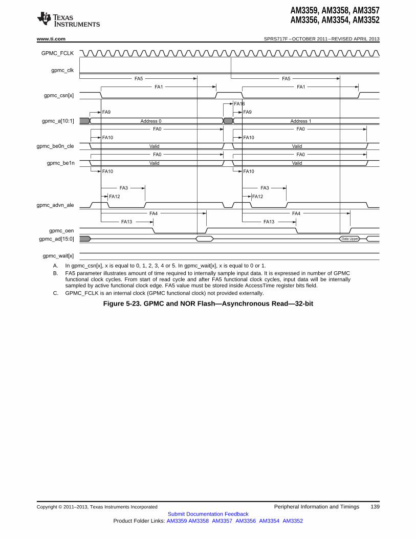
GPMC_FCLK
gpmc_clk
gpmc_csn[x]
gpmc_a[10:1]
gpmc_be0n_cle
gpmc_be1n
gpmc_advn_ale
gpmc_oen
gpmc_ad[15:0]
gpmc_wait[x]
Address 0 Address 1
Valid Valid
Valid Valid
Data Upper
FA9
FA10
FA3
FA9
FA3
FA13 FA13
FA1 FA1
FA4 FA4
FA12 FA12
FA10
FA0 FA0
FA16
FA0 FA0
FA10 FA10
FA5 FA5
AM3359, AM3358, AM3357AM3356, AM3354, AM3352
www.ti.com SPRS717F –OCTOBER 2011–REVISED APRIL 2013
A. In gpmc_csn[x], x is equal to 0, 1, 2, 3, 4 or 5. In gpmc_wait[x], x is equal to 0 or 1.B. FA5 parameter illustrates amount of time required to internally sample input data. It is expressed in number of GPMC
functional clock cycles. From start of read cycle and after FA5 functional clock cycles, input data will be internallysampled by active functional clock edge. FA5 value must be stored inside AccessTime register bits field.
C. GPMC_FCLK is an internal clock (GPMC functional clock) not provided externally.
Figure 5-23. GPMC and NOR Flash—Asynchronous Read—32-bit
Copyright © 2011–2013, Texas Instruments Incorporated Peripheral Information and Timings 139Submit Documentation Feedback
Product Folder Links: AM3359 AM3358 AM3357 AM3356 AM3354 AM3352
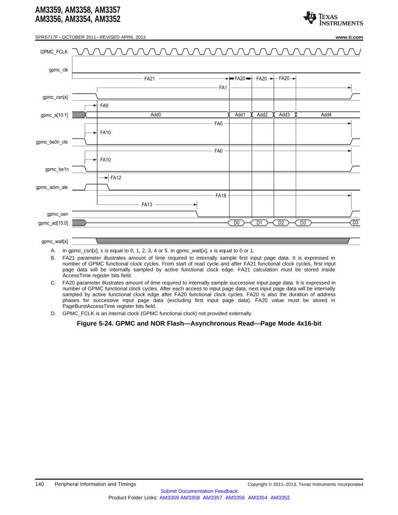
GPMC_FCLK
gpmc_clk
gpmc_csn[x]
gpmc_a[10:1]
gpmc_be0n_cle
gpmc_be1n
gpmc_advn_ale
gpmc_oen
gpmc_ad[15:0]
gpmc_wait[x]
Add0 Add1 Add2 Add3 Add4
D0 D1 D2 D3 D3
FA1
FA0
FA18
FA13
FA12
FA0
FA9
FA10
FA10
FA21 FA20 FA20FA20
AM3359, AM3358, AM3357AM3356, AM3354, AM3352
SPRS717F –OCTOBER 2011–REVISED APRIL 2013 www.ti.com
A. In gpmc_csn[x], x is equal to 0, 1, 2, 3, 4 or 5. In gpmc_wait[x], x is equal to 0 or 1.B. FA21 parameter illustrates amount of time required to internally sample first input page data. It is expressed in
number of GPMC functional clock cycles. From start of read cycle and after FA21 functional clock cycles, first inputpage data will be internally sampled by active functional clock edge. FA21 calculation must be stored insideAccessTime register bits field.
C. FA20 parameter illustrates amount of time required to internally sample successive input page data. It is expressed innumber of GPMC functional clock cycles. After each access to input page data, next input page data will be internallysampled by active functional clock edge after FA20 functional clock cycles. FA20 is also the duration of addressphases for successive input page data (excluding first input page data). FA20 value must be stored inPageBurstAccessTime register bits field.
D. GPMC_FCLK is an internal clock (GPMC functional clock) not provided externally.
Figure 5-24. GPMC and NOR Flash—Asynchronous Read—Page Mode 4x16-bit
140 Peripheral Information and Timings Copyright © 2011–2013, Texas Instruments Incorporated
Submit Documentation FeedbackProduct Folder Links: AM3359 AM3358 AM3357 AM3356 AM3354 AM3352
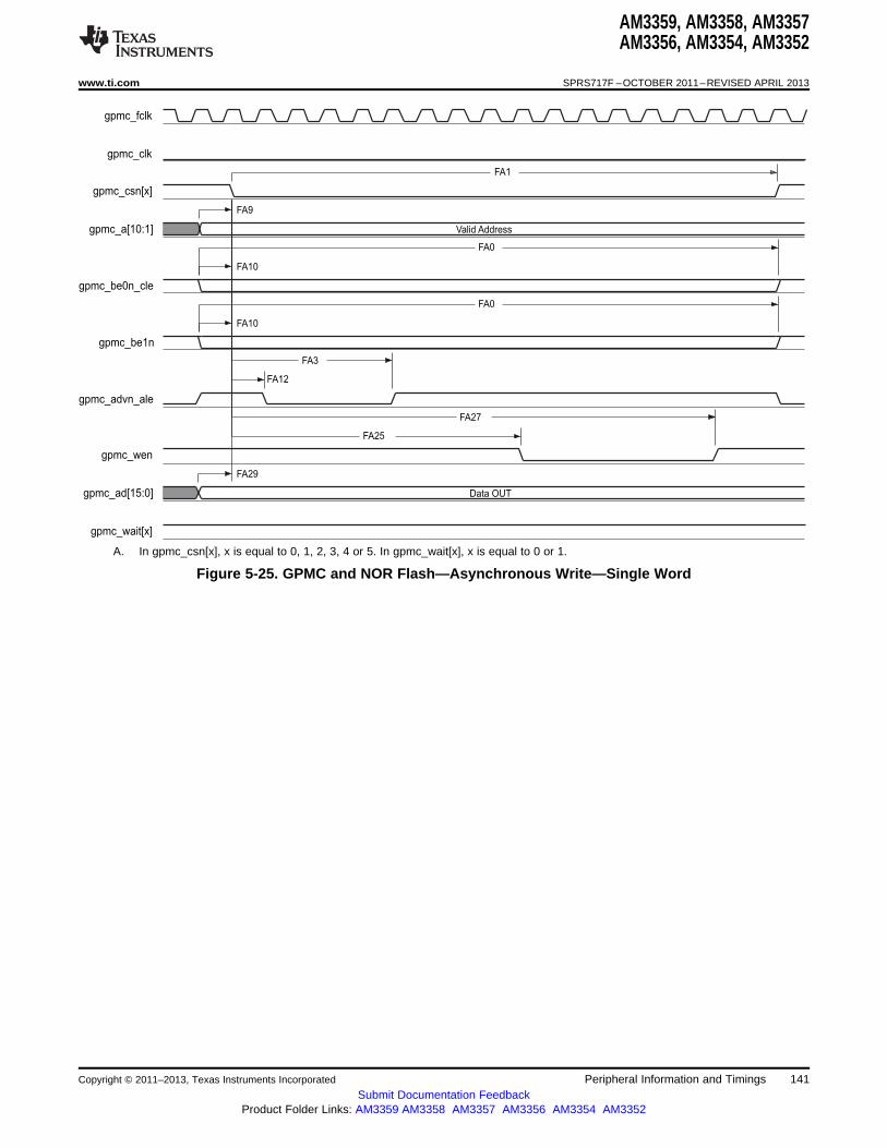
gpmc_fclk
gpmc_clk
gpmc_csn[x]
gpmc_a[10:1]
gpmc_be0n_cle
gpmc_be1n
gpmc_advn_ale
gpmc_wen
gpmc_ad[15:0]
gpmc_wait[x]
Valid Address
Data OUT
FA0
FA1
FA10
FA3
FA25
FA29
FA9
FA12
FA27
FA0
FA10
AM3359, AM3358, AM3357AM3356, AM3354, AM3352
www.ti.com SPRS717F –OCTOBER 2011–REVISED APRIL 2013
A. In gpmc_csn[x], x is equal to 0, 1, 2, 3, 4 or 5. In gpmc_wait[x], x is equal to 0 or 1.
Figure 5-25. GPMC and NOR Flash—Asynchronous Write—Single Word
Copyright © 2011–2013, Texas Instruments Incorporated Peripheral Information and Timings 141Submit Documentation Feedback
Product Folder Links: AM3359 AM3358 AM3357 AM3356 AM3354 AM3352
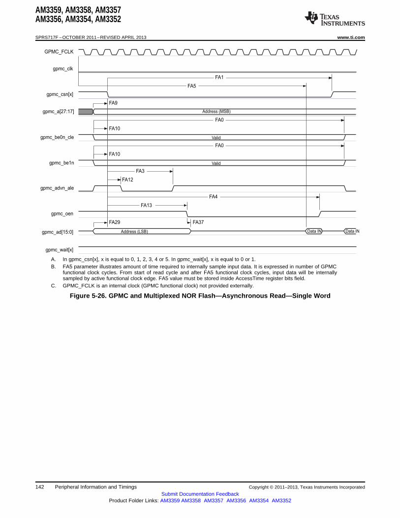
GPMC_FCLK
gpmc_clk
gpmc_csn[x]
gpmc_be0n_cle
gpmc_be1n
gpmc_advn_ale
gpmc_oen
gpmc_wait[x]
Address (MSB)
Valid
Valid
Address (LSB) Data IN Data IN
FA0
FA9
FA10
FA3
FA13
FA29
FA1
FA37
FA12
FA4
FA10
FA0
FA5
gpmc_a[27:17]
gpmc_ad[15:0]
AM3359, AM3358, AM3357AM3356, AM3354, AM3352
SPRS717F –OCTOBER 2011–REVISED APRIL 2013 www.ti.com
A. In gpmc_csn[x], x is equal to 0, 1, 2, 3, 4 or 5. In gpmc_wait[x], x is equal to 0 or 1.B. FA5 parameter illustrates amount of time required to internally sample input data. It is expressed in number of GPMC
functional clock cycles. From start of read cycle and after FA5 functional clock cycles, input data will be internallysampled by active functional clock edge. FA5 value must be stored inside AccessTime register bits field.
C. GPMC_FCLK is an internal clock (GPMC functional clock) not provided externally.
Figure 5-26. GPMC and Multiplexed NOR Flash—Asynchronous Read—Single Word
142 Peripheral Information and Timings Copyright © 2011–2013, Texas Instruments Incorporated
Submit Documentation FeedbackProduct Folder Links: AM3359 AM3358 AM3357 AM3356 AM3354 AM3352
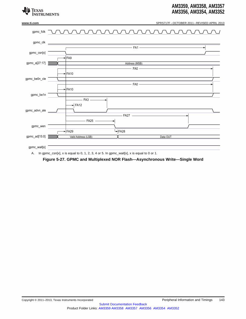
gpmc_fclk
gpmc_clk
gpmc_csn[x]
gpmc_a[27:17]
gpmc_be0n_cle
gpmc_be1n
gpmc_advn_ale
gpmc_wen
gpmc_ad[15:0]
gpmc_wait[x]
Address (MSB)
Valid Address (LSB) Data OUT
FA0
FA1
FA9
FA10
FA3
FA25
FA29
FA12
FA27
FA28
FA0
FA10
AM3359, AM3358, AM3357AM3356, AM3354, AM3352
www.ti.com SPRS717F –OCTOBER 2011–REVISED APRIL 2013
A. In gpmc_csn[x], x is equal to 0, 1, 2, 3, 4 or 5. In gpmc_wait[x], x is equal to 0 or 1.
Figure 5-27. GPMC and Multiplexed NOR Flash—Asynchronous Write—Single Word
Copyright © 2011–2013, Texas Instruments Incorporated Peripheral Information and Timings 143Submit Documentation Feedback
Product Folder Links: AM3359 AM3358 AM3357 AM3356 AM3354 AM3352
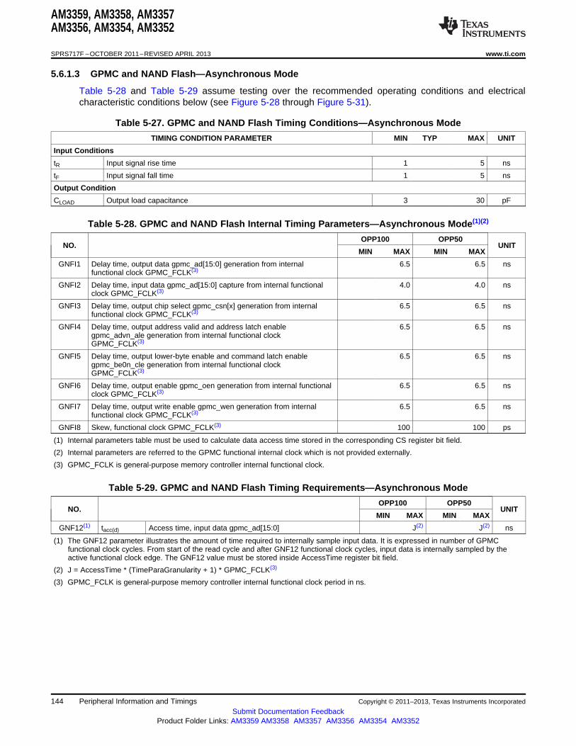
AM3359, AM3358, AM3357AM3356, AM3354, AM3352
SPRS717F –OCTOBER 2011–REVISED APRIL 2013 www.ti.com
5.6.1.3 GPMC and NAND Flash—Asynchronous Mode
Table 5-28 and Table 5-29 assume testing over the recommended operating conditions and electricalcharacteristic conditions below (see Figure 5-28 through Figure 5-31).
Table 5-27. GPMC and NAND Flash Timing Conditions—Asynchronous Mode
TIMING CONDITION PARAMETER MIN TYP MAX UNIT
Input Conditions
tR Input signal rise time 1 5 ns
tF Input signal fall time 1 5 ns
Output Condition
CLOAD Output load capacitance 3 30 pF
Table 5-28. GPMC and NAND Flash Internal Timing Parameters—Asynchronous Mode(1)(2)
OPP100 OPP50NO. UNIT
MIN MAX MIN MAX
GNFI1 Delay time, output data gpmc_ad[15:0] generation from internal 6.5 6.5 nsfunctional clock GPMC_FCLK(3)
GNFI2 Delay time, input data gpmc_ad[15:0] capture from internal functional 4.0 4.0 nsclock GPMC_FCLK(3)
GNFI3 Delay time, output chip select gpmc_csn[x] generation from internal 6.5 6.5 nsfunctional clock GPMC_FCLK(3)
GNFI4 Delay time, output address valid and address latch enable 6.5 6.5 nsgpmc_advn_ale generation from internal functional clockGPMC_FCLK(3)
GNFI5 Delay time, output lower-byte enable and command latch enable 6.5 6.5 nsgpmc_be0n_cle generation from internal functional clockGPMC_FCLK(3)
GNFI6 Delay time, output enable gpmc_oen generation from internal functional 6.5 6.5 nsclock GPMC_FCLK(3)
GNFI7 Delay time, output write enable gpmc_wen generation from internal 6.5 6.5 nsfunctional clock GPMC_FCLK(3)
GNFI8 Skew, functional clock GPMC_FCLK(3) 100 100 ps
(1) Internal parameters table must be used to calculate data access time stored in the corresponding CS register bit field.
(2) Internal parameters are referred to the GPMC functional internal clock which is not provided externally.
(3) GPMC_FCLK is general-purpose memory controller internal functional clock.
Table 5-29. GPMC and NAND Flash Timing Requirements—Asynchronous Mode
OPP100 OPP50NO. UNIT
MIN MAX MIN MAX
GNF12(1) tacc(d) Access time, input data gpmc_ad[15:0] J(2) J(2) ns
(1) The GNF12 parameter illustrates the amount of time required to internally sample input data. It is expressed in number of GPMCfunctional clock cycles. From start of the read cycle and after GNF12 functional clock cycles, input data is internally sampled by theactive functional clock edge. The GNF12 value must be stored inside AccessTime register bit field.
(2) J = AccessTime * (TimeParaGranularity + 1) * GPMC_FCLK(3)
(3) GPMC_FCLK is general-purpose memory controller internal functional clock period in ns.
144 Peripheral Information and Timings Copyright © 2011–2013, Texas Instruments Incorporated
Submit Documentation FeedbackProduct Folder Links: AM3359 AM3358 AM3357 AM3356 AM3354 AM3352
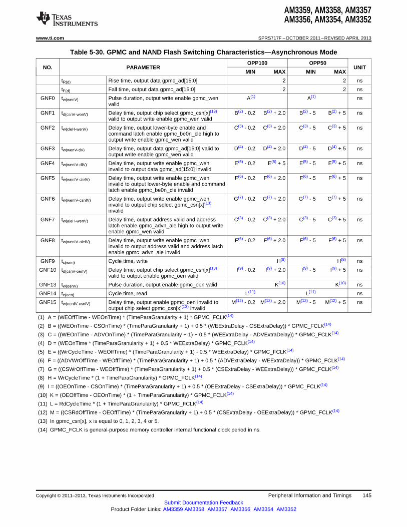
AM3359, AM3358, AM3357AM3356, AM3354, AM3352
www.ti.com SPRS717F –OCTOBER 2011–REVISED APRIL 2013
Table 5-30. GPMC and NAND Flash Switching Characteristics—Asynchronous Mode
OPP100 OPP50NO. PARAMETER UNIT
MIN MAX MIN MAX
tR(d) Rise time, output data gpmc_ad[15:0] 2 2 ns
tF(d) Fall time, output data gpmc_ad[15:0] 2 2 ns
GNF0 tw(wenV) Pulse duration, output write enable gpmc_wen A(1) A(1) nsvalid
GNF1 td(csnV-wenV) Delay time, output chip select gpmc_csn[x](13) B(2) - 0.2 B(2) + 2.0 B(2) - 5 B(2) + 5 nsvalid to output write enable gpmc_wen valid
GNF2 tw(cleH-wenV) Delay time, output lower-byte enable and C(3) - 0.2 C(3) + 2.0 C(3) - 5 C(3) + 5 nscommand latch enable gpmc_be0n_cle high tooutput write enable gpmc_wen valid
GNF3 tw(wenV-dV) Delay time, output data gpmc_ad[15:0] valid to D(4) - 0.2 D(4) + 2.0 D(4) - 5 D(4) + 5 nsoutput write enable gpmc_wen valid
GNF4 tw(wenIV-dIV) Delay time, output write enable gpmc_wen E(5) - 0.2 E(5) + 5 E(5) - 5 E(5) + 5 nsinvalid to output data gpmc_ad[15:0] invalid
GNF5 tw(wenIV-cleIV) Delay time, output write enable gpmc_wen F(6) - 0.2 F(6) + 2.0 F(6) - 5 F(6) + 5 nsinvalid to output lower-byte enable and commandlatch enable gpmc_be0n_cle invalid
GNF6 tw(wenIV-csnIV) Delay time, output write enable gpmc_wen G(7) - 0.2 G(7) + 2.0 G(7) - 5 G(7) + 5 nsinvalid to output chip select gpmc_csn[x](13)
invalid
GNF7 tw(aleH-wenV) Delay time, output address valid and address C(3) - 0.2 C(3) + 2.0 C(3) - 5 C(3) + 5 nslatch enable gpmc_advn_ale high to output writeenable gpmc_wen valid
GNF8 tw(wenIV-aleIV) Delay time, output write enable gpmc_wen F(6) - 0.2 F(6) + 2.0 F(6) - 5 F(6) + 5 nsinvalid to output address valid and address latchenable gpmc_advn_ale invalid
GNF9 tc(wen) Cycle time, write H(8) H(8) ns
GNF10 td(csnV-oenV) Delay time, output chip select gpmc_csn[x](13) I(9) - 0.2 I(9) + 2.0 I(9) - 5 I(9) + 5 nsvalid to output enable gpmc_oen valid
GNF13 tw(oenV) Pulse duration, output enable gpmc_oen valid K(10) K(10) ns
GNF14 tc(oen) Cycle time, read L(11) L(11) ns
GNF15 tw(oenIV-csnIV) Delay time, output enable gpmc_oen invalid to M(12) - 0.2 M(12) + 2.0 M(12) - 5 M(12) + 5 nsoutput chip select gpmc_csn[x](13) invalid
(1) A = (WEOffTime - WEOnTime) * (TimeParaGranularity + 1) * GPMC_FCLK(14)
(2) B = ((WEOnTime - CSOnTime) * (TimeParaGranularity + 1) + 0.5 * (WEExtraDelay - CSExtraDelay)) * GPMC_FCLK(14)
(3) C = ((WEOnTime - ADVOnTime) * (TimeParaGranularity + 1) + 0.5 * (WEExtraDelay - ADVExtraDelay)) * GPMC_FCLK(14)
(4) D = (WEOnTime * (TimeParaGranularity + 1) + 0.5 * WEExtraDelay) * GPMC_FCLK(14)
(5) E = ((WrCycleTime - WEOffTime) * (TimeParaGranularity + 1) - 0.5 * WEExtraDelay) * GPMC_FCLK(14)
(6) F = ((ADVWrOffTime - WEOffTime) * (TimeParaGranularity + 1) + 0.5 * (ADVExtraDelay - WEExtraDelay)) * GPMC_FCLK(14)
(7) G = ((CSWrOffTime - WEOffTime) * (TimeParaGranularity + 1) + 0.5 * (CSExtraDelay - WEExtraDelay)) * GPMC_FCLK(14)
(8) H = WrCycleTime * (1 + TimeParaGranularity) * GPMC_FCLK(14)
(9) I = ((OEOnTime - CSOnTime) * (TimeParaGranularity + 1) + 0.5 * (OEExtraDelay - CSExtraDelay)) * GPMC_FCLK(14)
(10) K = (OEOffTime - OEOnTime) * (1 + TimeParaGranularity) * GPMC_FCLK(14)
(11) L = RdCycleTime * (1 + TimeParaGranularity) * GPMC_FCLK(14)
(12) M = ((CSRdOffTime - OEOffTime) * (TimeParaGranularity + 1) + 0.5 * (CSExtraDelay - OEExtraDelay)) * GPMC_FCLK(14)
(13) In gpmc_csn[x], x is equal to 0, 1, 2, 3, 4 or 5.
(14) GPMC_FCLK is general-purpose memory controller internal functional clock period in ns.
Copyright © 2011–2013, Texas Instruments Incorporated Peripheral Information and Timings 145Submit Documentation Feedback
Product Folder Links: AM3359 AM3358 AM3357 AM3356 AM3354 AM3352
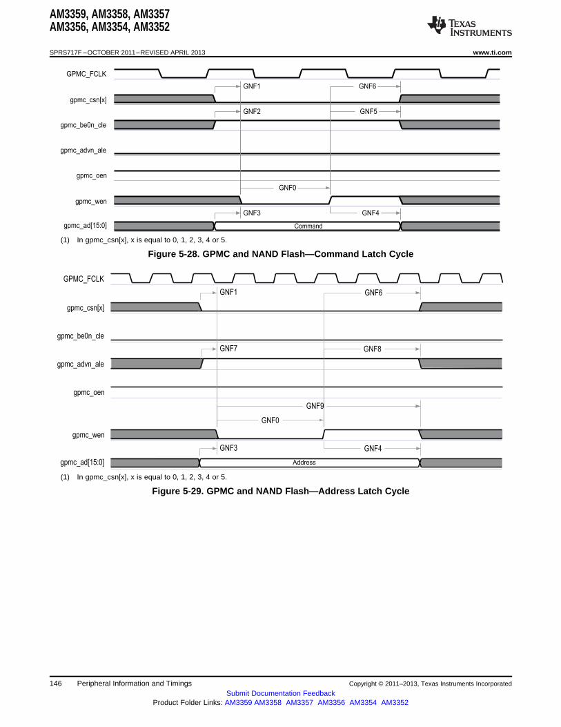
GPMC_FCLK
gpmc_csn[x]
gpmc_be0n_cle
gpmc_advn_ale
gpmc_oen
gpmc_wen
gpmc_ad[15:0] Address
GNF0
GNF1
GNF7
GNF3 GNF4
GNF6
GNF8
GNF9
GPMC_FCLK
gpmc_csn[x]
gpmc_be0n_cle
gpmc_advn_ale
gpmc_oen
gpmc_wen
gpmc_ad[15:0] Command
GNF0
GNF1
GNF2
GNF3 GNF4
GNF5
GNF6
AM3359, AM3358, AM3357AM3356, AM3354, AM3352
SPRS717F –OCTOBER 2011–REVISED APRIL 2013 www.ti.com
(1) In gpmc_csn[x], x is equal to 0, 1, 2, 3, 4 or 5.
Figure 5-28. GPMC and NAND Flash—Command Latch Cycle
(1) In gpmc_csn[x], x is equal to 0, 1, 2, 3, 4 or 5.
Figure 5-29. GPMC and NAND Flash—Address Latch Cycle
146 Peripheral Information and Timings Copyright © 2011–2013, Texas Instruments Incorporated
Submit Documentation FeedbackProduct Folder Links: AM3359 AM3358 AM3357 AM3356 AM3354 AM3352

GPMC_FCLK
gpmc_csn[x]
gpmc_be0n_cle
gpmc_advn_ale
gpmc_oen
gpmc_wen
DATA
GNF0
GNF1
GNF4
GNF9
GNF3
GNF6
gpmc_ad[15:0]
GPMC_FCLK
gpmc_csn[x]
gpmc_be0n_cle
gpmc_advn_ale
gpmc_oen
gpmc_wait[x]
DATA
GNF10
GNF14
GNF15
GNF12
GNF13
gpmc_ad[15:0]
AM3359, AM3358, AM3357AM3356, AM3354, AM3352
www.ti.com SPRS717F –OCTOBER 2011–REVISED APRIL 2013
(1) GNF12 parameter illustrates amount of time required to internally sample input data. It is expressed in number of GPMC functionalclock cycles. From start of read cycle and after GNF12 functional clock cycles, input data will be internally sampled by activefunctional clock edge. GNF12 value must be stored inside AccessTime register bits field.
(2) GPMC_FCLK is an internal clock (GPMC functional clock) not provided externally.(3) In gpmc_csn[x], x is equal to 0, 1, 2, 3, 4 or 5. In gpmc_wait[x], x is equal to 0 or 1.
Figure 5-30. GPMC and NAND Flash—Data Read Cycle
(1) In gpmc_csn[x], x is equal to 0, 1, 2, 3, 4 or 5.
Figure 5-31. GPMC and NAND Flash—Data Write Cycle
Copyright © 2011–2013, Texas Instruments Incorporated Peripheral Information and Timings 147Submit Documentation Feedback
Product Folder Links: AM3359 AM3358 AM3357 AM3356 AM3354 AM3352
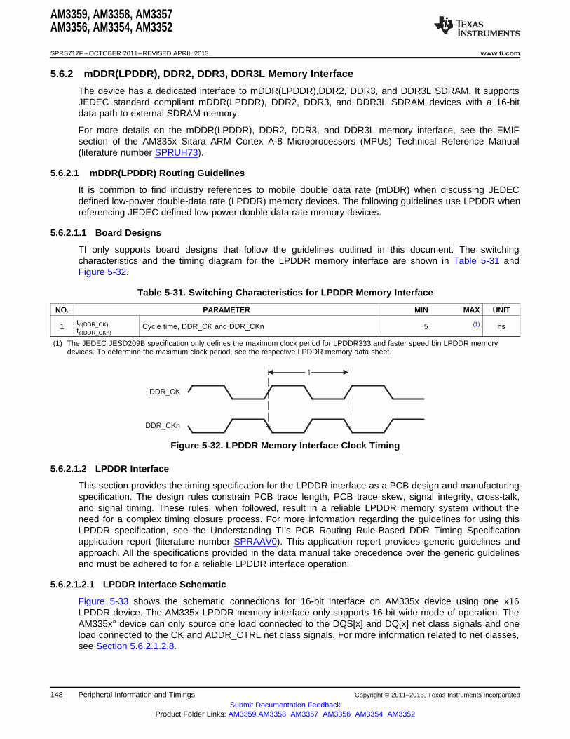
DDR_CK
1
DDR_CKn
AM3359, AM3358, AM3357AM3356, AM3354, AM3352
SPRS717F –OCTOBER 2011–REVISED APRIL 2013 www.ti.com
5.6.2 mDDR(LPDDR), DDR2, DDR3, DDR3L Memory Interface
The device has a dedicated interface to mDDR(LPDDR),DDR2, DDR3, and DDR3L SDRAM. It supportsJEDEC standard compliant mDDR(LPDDR), DDR2, DDR3, and DDR3L SDRAM devices with a 16-bitdata path to external SDRAM memory.
For more details on the mDDR(LPDDR), DDR2, DDR3, and DDR3L memory interface, see the EMIFsection of the AM335x Sitara ARM Cortex A-8 Microprocessors (MPUs) Technical Reference Manual(literature number SPRUH73).
5.6.2.1 mDDR(LPDDR) Routing Guidelines
It is common to find industry references to mobile double data rate (mDDR) when discussing JEDECdefined low-power double-data rate (LPDDR) memory devices. The following guidelines use LPDDR whenreferencing JEDEC defined low-power double-data rate memory devices.
5.6.2.1.1 Board Designs
TI only supports board designs that follow the guidelines outlined in this document. The switchingcharacteristics and the timing diagram for the LPDDR memory interface are shown in Table 5-31 andFigure 5-32.
Table 5-31. Switching Characteristics for LPDDR Memory Interface
NO. PARAMETER MIN MAX UNIT
tc(DDR_CK)1 Cycle time, DDR_CK and DDR_CKn 5 (1) nstc(DDR_CKn)
(1) The JEDEC JESD209B specification only defines the maximum clock period for LPDDR333 and faster speed bin LPDDR memorydevices. To determine the maximum clock period, see the respective LPDDR memory data sheet.
Figure 5-32. LPDDR Memory Interface Clock Timing
5.6.2.1.2 LPDDR Interface
This section provides the timing specification for the LPDDR interface as a PCB design and manufacturingspecification. The design rules constrain PCB trace length, PCB trace skew, signal integrity, cross-talk,and signal timing. These rules, when followed, result in a reliable LPDDR memory system without theneed for a complex timing closure process. For more information regarding the guidelines for using thisLPDDR specification, see the Understanding TI’s PCB Routing Rule-Based DDR Timing Specificationapplication report (literature number SPRAAV0). This application report provides generic guidelines andapproach. All the specifications provided in the data manual take precedence over the generic guidelinesand must be adhered to for a reliable LPDDR interface operation.
5.6.2.1.2.1 LPDDR Interface Schematic
Figure 5-33 shows the schematic connections for 16-bit interface on AM335x device using one x16LPDDR device. The AM335x LPDDR memory interface only supports 16-bit wide mode of operation. TheAM335x° device can only source one load connected to the DQS[x] and DQ[x] net class signals and oneload connected to the CK and ADDR_CTRL net class signals. For more information related to net classes,see Section 5.6.2.1.2.8.
148 Peripheral Information and Timings Copyright © 2011–2013, Texas Instruments Incorporated
Submit Documentation FeedbackProduct Folder Links: AM3359 AM3358 AM3357 AM3356 AM3354 AM3352
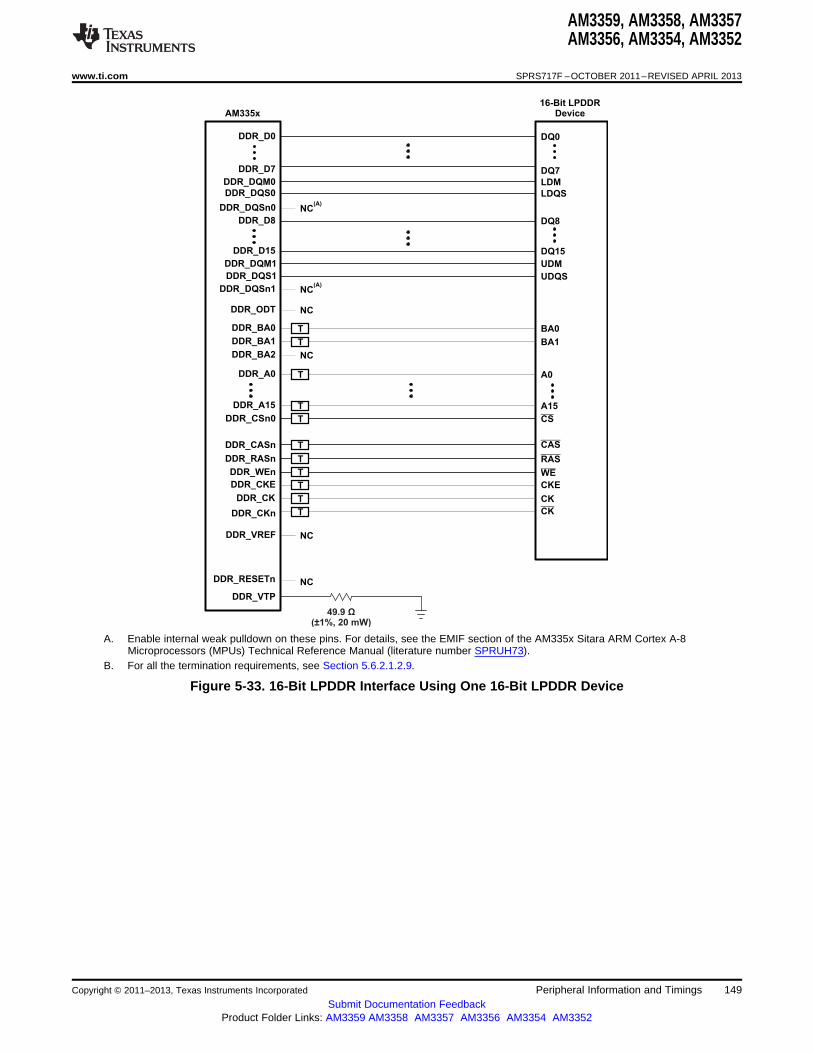
DDR_D0
DDR_D7
DDR_DQM0
DDR_DQS0
DDR_DQSn0
DDR_D8
DDR_D15
DDR_DQM1
DDR_DQS1
DDR_DQSn1
DQ0
DQ7
LDM
LDQS
DQ8
DQ15
UDM
UDQS
BA0
A0
A15
CS
CAS
RAS
WE
CKE
CK
CK
DDR_BA0
DDR_A0
DDR_A15
DDR_CSn0
DDR_CASn
DDR_RASn
DDR_WEn
DDR_CKE
DDR_CK
DDR_CKn
DDR_VREF
16-Bit LPDDRDevice
DDR_VTP
49.9( 1%, 20 mW)
Ω±
DDR_ODT
DDR_RESETn NC
AM335x
T
T
T
T
T
T
T
T
T
T
BA1DDR_BA1
DDR_BA2
NC
NC
T
NC(A)
NC(A)
NC
AM3359, AM3358, AM3357AM3356, AM3354, AM3352
www.ti.com SPRS717F –OCTOBER 2011–REVISED APRIL 2013
A. Enable internal weak pulldown on these pins. For details, see the EMIF section of the AM335x Sitara ARM Cortex A-8Microprocessors (MPUs) Technical Reference Manual (literature number SPRUH73).
B. For all the termination requirements, see Section 5.6.2.1.2.9.
Figure 5-33. 16-Bit LPDDR Interface Using One 16-Bit LPDDR Device
Copyright © 2011–2013, Texas Instruments Incorporated Peripheral Information and Timings 149Submit Documentation Feedback
Product Folder Links: AM3359 AM3358 AM3357 AM3356 AM3354 AM3352

AM3359, AM3358, AM3357AM3356, AM3354, AM3352
SPRS717F –OCTOBER 2011–REVISED APRIL 2013 www.ti.com
5.6.2.1.2.2 Compatible JEDEC LPDDR Devices
Table 5-32 shows the parameters of the JEDEC LPDDR devices that are compatible with this interface.Generally, the LPDDR interface is compatible with x16 LPDDR400 speed grade LPDDR devices.
Table 5-32. Compatible JEDEC LPDDR Devices (Per Interface)(1)
NO. PARAMETER MIN MAX UNIT
1 JEDEC LPDDR device speed grade LPDDR400
2 JEDEC LPDDR device bit width x16 x16 Bits
3 JEDEC LPDDR device count 1 Devices
4 JEDEC LPDDR device terminal count 60 Terminals
(1) If the LPDDR interface is operated with a clock frequency less than 200 MHz, lower-speed grade LPDDR devices may be used if theminimum clock period specified for the LPDDR device is less than or equal to the minimum clock period selected for the AM335xLPDDR interface.
5.6.2.1.2.3 PCB Stackup
The minimum stackup required for routing the AM335x device is a four-layer stackup as shown in Table 5-33. Additional layers may be added to the PCB stackup to accommodate other circuitry, enhance signalintegrity and electromagnetic interference performance, or to reduce the size of the PCB footprint.
Table 5-33. Minimum PCB Stackup(1)
LAYER TYPE DESCRIPTION
1 Signal Top signal routing
2 Plane Ground
3 Plane Split Power Plane
4 Signal Bottom signal routing
(1) All signals that have critical signal integrity requirements should be routed first on layer 1. It may not be possible to route all of thesesignals on layer 1 which requires some to be routed on layer 4. When this is done, the signal routes on layer 4 should not cross splits inthe power plane.
150 Peripheral Information and Timings Copyright © 2011–2013, Texas Instruments Incorporated
Submit Documentation FeedbackProduct Folder Links: AM3359 AM3358 AM3357 AM3356 AM3354 AM3352
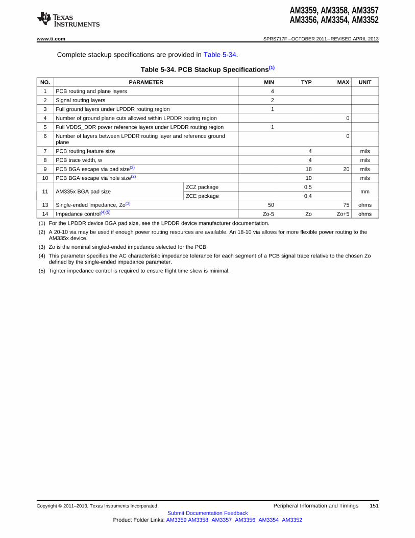
AM3359, AM3358, AM3357AM3356, AM3354, AM3352
www.ti.com SPRS717F –OCTOBER 2011–REVISED APRIL 2013
Complete stackup specifications are provided in Table 5-34.
Table 5-34. PCB Stackup Specifications(1)
NO. PARAMETER MIN TYP MAX UNIT
1 PCB routing and plane layers 4
2 Signal routing layers 2
3 Full ground layers under LPDDR routing region 1
4 Number of ground plane cuts allowed within LPDDR routing region 0
5 Full VDDS_DDR power reference layers under LPDDR routing region 1
6 Number of layers between LPDDR routing layer and reference ground 0plane
7 PCB routing feature size 4 mils
8 PCB trace width, w 4 mils
9 PCB BGA escape via pad size(2) 18 20 mils
10 PCB BGA escape via hole size(2) 10 mils
ZCZ package 0.511 AM335x BGA pad size mm
ZCE package 0.4
13 Single-ended impedance, Zo(3) 50 75 ohms
14 Impedance control(4)(5) Zo-5 Zo Zo+5 ohms
(1) For the LPDDR device BGA pad size, see the LPDDR device manufacturer documentation.
(2) A 20-10 via may be used if enough power routing resources are available. An 18-10 via allows for more flexible power routing to theAM335x device.
(3) Zo is the nominal singled-ended impedance selected for the PCB.
(4) This parameter specifies the AC characteristic impedance tolerance for each segment of a PCB signal trace relative to the chosen Zodefined by the single-ended impedance parameter.
(5) Tighter impedance control is required to ensure flight time skew is minimal.
Copyright © 2011–2013, Texas Instruments Incorporated Peripheral Information and Timings 151Submit Documentation Feedback
Product Folder Links: AM3359 AM3358 AM3357 AM3356 AM3354 AM3352

A1
A1
X
Y
OFFSET
Recommended LPDDR
Device Orientation
Y
Y
OFFSET
LPDDR
Device
LP
DD
R
Inte
rfa
ce
AM335x
AM3359, AM3358, AM3357AM3356, AM3354, AM3352
SPRS717F –OCTOBER 2011–REVISED APRIL 2013 www.ti.com
5.6.2.1.2.4 Placement
Figure 5-34 shows the required placement for the LPDDR devices. The dimensions for this figure aredefined in Table 5-35. The placement does not restrict the side of the PCB on which the devices aremounted. The ultimate purpose of the placement is to limit the maximum trace lengths and allow forproper routing space. For single-memory LPDDR systems, the second LPDDR device is omitted from theplacement.
Figure 5-34. AM335x Device and LPDDR Device Placement
Table 5-35. Placement Specifications(1)
NO. PARAMETER MIN MAX UNIT
1 X(2)(3) 1750 mils
2 Y(2)(3) 1280 mils
3 Y Offset(2)(3)(4) 650 mils
4 Clearance from non-LPDDR signal to LPDDR keepout region(5)(6) 4 w
(1) LPDDR keepout region to encompass entire LPDDR routing area.
(2) For dimension definitions, see Figure 5-34.
(3) Measurements from center of AM335x device to center of LPDDR device.
(4) For single-memory systems, it is recommended that Y offset be as small as possible.
(5) w is defined as the signal trace width.
(6) Non-LPDDR signals allowed within LPDDR keepout region provided they are separated from LPDDR routing layers by a ground plane.
152 Peripheral Information and Timings Copyright © 2011–2013, Texas Instruments Incorporated
Submit Documentation FeedbackProduct Folder Links: AM3359 AM3358 AM3357 AM3356 AM3354 AM3352

A1
A1
LP
DD
RIn
terfa
ce
LPDDRDevice
AM3359, AM3358, AM3357AM3356, AM3354, AM3352
www.ti.com SPRS717F –OCTOBER 2011–REVISED APRIL 2013
5.6.2.1.2.5 LPDDR Keepout Region
The region of the PCB used for the LPDDR circuitry must be isolated from other signals. The LPDDRkeepout region is defined for this purpose and is shown in Figure 5-35. This region should encompass allLPDDR circuitry and the region size varies with component placement and LPDDR routing. Additionalclearances required for the keepout region are shown in Table 5-35. Non-LPDDR signals should not berouted on the same signal layer as LPDDR signals within the LPDDR keepout region. Non-LPDDR signalsmay be routed in the region provided they are routed on layers separated from LPDDR signal layers by aground layer. No breaks should be allowed in the reference ground or VDDS_DDR power plane in thisregion. In addition, the VDDS_DDR power plane should cover the entire keepout region.
Figure 5-35. LPDDR Keepout Region
5.6.2.1.2.6 Bulk Bypass Capacitors
Bulk bypass capacitors are required for moderate speed bypassing of the LPDDR and other circuitry.Table 5-36 contains the minimum numbers and capacitance required for the bulk bypass capacitors. Notethat this table only covers the bypass needs of the AM335x LPDDR interface and LPDDR devices.Additional bulk bypass capacitance may be needed for other circuitry.
Table 5-36. Bulk Bypass Capacitors(1)
NO. PARAMETER MIN MAX UNIT
1 AM335x VDDS_DDR bulk bypass capacitor count 1 Devices
2 AM335x VDDS_DDR bulk bypass total capacitance 10 μF
3 LPDDR#1 bulk bypass capacitor count 1 Devices
4 LPDDR#1 bulk bypass total capacitance 10 μF
5 LPDDR#2 bulk bypass capacitor count(2) 1 Devices
6 LPDDR#2 bulk bypass total capacitance(2) 10 μF
(1) These devices should be placed near the device they are bypassing, but preference should be given to the placement of the high-speed(HS) bypass capacitors.
(2) Only used when two LPDDR devices are used.
Copyright © 2011–2013, Texas Instruments Incorporated Peripheral Information and Timings 153Submit Documentation Feedback
Product Folder Links: AM3359 AM3358 AM3357 AM3356 AM3354 AM3352

AM3359, AM3358, AM3357AM3356, AM3354, AM3352
SPRS717F –OCTOBER 2011–REVISED APRIL 2013 www.ti.com
5.6.2.1.2.7 High-Speed Bypass Capacitors
High-speed (HS) bypass capacitors are critical for proper LPDDR interface operation. It is particularlyimportant to minimize the parasitic series inductance of the HS bypass capacitors, AM335x device LPDDRpower, and AM335x device LPDDR ground connections. Table 5-37 contains the specification for the HSbypass capacitors as well as for the power connections on the PCB.
Table 5-37. High-Speed Bypass Capacitors
NO. PARAMETER MIN MAX UNIT
1 HS bypass capacitor package size(1) 0402 10 mils
2 Distance from HS bypass capacitor to device being bypassed 250 mils
3 Number of connection vias for each HS bypass capacitor(2) 2 Vias
4 Trace length from bypass capacitor contact to connection via 30 mils
5 Number of connection vias for each AM335x VDDS_DDR and VSS terminal 1 Vias
6 Trace length from AM335x VDDS_DDR and VSS terminal to connection via 35 mils
7 Number of connection vias for each LPDDR device power and ground terminal 1 Vias
8 Trace length from LPDDR device power and ground terminal to connection via 35 mils
9 AM335x VDDS_DDR HS bypass capacitor count(3) 10 Devices
10 AM335x VDDS_DDR HS bypass capacitor total capacitance 0.6 μF
11 LPDDR device HS bypass capacitor count(3)(4) 8 Devices
12 LPDDR device HS bypass capacitor total capacitance(4) 0.4 μF
(1) LxW, 10-mil units; for example, a 0402 is a 40x20-mil surface-mount capacitor.
(2) An additional HS bypass capacitor can share the connection vias only if it is mounted on the opposite side of the board.
(3) These devices should be placed as close as possible to the device being bypassed.
(4) Per LPDDR device.
5.6.2.1.2.8 Net Classes
Table 5-38 lists the clock net classes for the LPDDR interface. Table 5-39 lists the signal net classes, andassociated clock net classes, for the signals in the LPDDR interface. These net classes are used for thetermination and routing rules that follow.
Table 5-38. Clock Net Class Definitions
CLOCK NET CLASS AM335x PIN NAMES
CK DDR_CK and DDR_CKn
DQS0 DDR_DQS0
DQS1 DDR_DQS1
Table 5-39. Signal Net Class Definitions
ASSOCIATED CLOCKSIGNAL NET CLASS AM335x PIN NAMESNET CLASS
ADDR_CTRL CK DDR_BA[1:0], DDR_A[15:0], DDR_CSn0, DDR_CASn, DDR_RASn,DDR_WEn, DDR_CKE
DQ0 DQS0 DDR_D[7:0], DDR_DQM0
DQ1 DQS1 DDR_D[15:8], DDR_DQM1
154 Peripheral Information and Timings Copyright © 2011–2013, Texas Instruments Incorporated
Submit Documentation FeedbackProduct Folder Links: AM3359 AM3358 AM3357 AM3356 AM3354 AM3352
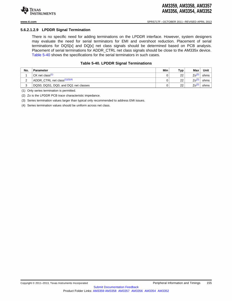
AM3359, AM3358, AM3357AM3356, AM3354, AM3352
www.ti.com SPRS717F –OCTOBER 2011–REVISED APRIL 2013
5.6.2.1.2.9 LPDDR Signal Termination
There is no specific need for adding terminations on the LPDDR interface. However, system designersmay evaluate the need for serial terminators for EMI and overshoot reduction. Placement of serialterminations for DQS[x] and DQ[x] net class signals should be determined based on PCB analysis.Placement of serial terminations for ADDR_CTRL net class signals should be close to the AM335x device.Table 5-40 shows the specifications for the serial terminators in such cases.
Table 5-40. LPDDR Signal Terminations
No. Parameter Min Typ Max Unit
1 CK net class(1) 0 22 Zo(2) ohms
2 ADDR_CTRL net class(1)(3)(4) 0 22 Zo(2) ohms
3 DQS0, DQS1, DQ0, and DQ1 net classes 0 22 Zo(2) ohms
(1) Only series termination is permitted.
(2) Zo is the LPDDR PCB trace characteristic impedance.
(3) Series termination values larger than typical only recommended to address EMI issues.
(4) Series termination values should be uniform across net class.
Copyright © 2011–2013, Texas Instruments Incorporated Peripheral Information and Timings 155Submit Documentation Feedback
Product Folder Links: AM3359 AM3358 AM3357 AM3356 AM3354 AM3352

A1
A1
CB
A
LP
DD
R
Inte
rfa
ce
AM335x
AM3359, AM3358, AM3357AM3356, AM3354, AM3352
SPRS717F –OCTOBER 2011–REVISED APRIL 2013 www.ti.com
5.6.2.1.3 LPDDR CK and ADDR_CTRL Routing
Figure 5-36 shows the topology of the routing for the CK and ADDR_CTRL net classes. The length ofsignal path AB and AC should be minimized with emphasis to minimize lengths C and D such that lengthA is the majority of the total length of signal path AB and AC.
Figure 5-36. CK and ADDR_CTRL Routing and Topology
Table 5-41. CK and ADDR_CTRL Routing Specification(1)(2)
NO. PARAMETER MIN TYP MAX UNIT
1 Center-to-center CK spacing 2w
2 CK differential pair skew length mismatch(2)(3) 25 mils
3 CK B-to-CK C skew length mismatch 25 mils
4 Center-to-center CK to other LPDDR trace spacing(4) 4w
5 CK and ADDR_CTRL nominal trace length(5) CACLM-50 CACLM CACLM+50 mils
6 ADDR_CTRL-to-CK skew length mismatch 100 mils
7 ADDR_CTRL-to-ADDR_CTRL skew length mismatch 100 mils
8 Center-to-center ADDR_CTRL to other LPDDR trace spacing(4) 4w
9 Center-to-center ADDR_CTRL to other ADDR_CTRL trace spacing(4) 3w
10 ADDR_CTRL A-to-B and ADDR_CTRL A-to-C skew length mismatch(2) 100 mils
11 ADDR_CTRL B-to-C skew length mismatch 100 mils
(1) CK represents the clock net class, and ADDR_CTRL represents the address and control signal net class.
(2) Series terminator, if used, should be located closest to the AM335x device.
(3) Differential impedance should be Zo x 2, where Zo is the single-ended impedance defined in Table 5-34.
(4) Center-to-center spacing is allowed to fall to minimum (w) for up to 500 mils of routed length to accommodate BGA escape and routingcongestion.
(5) CACLM is the longest Manhattan distance of the CK and ADDR_CTRL net classes.
156 Peripheral Information and Timings Copyright © 2011–2013, Texas Instruments Incorporated
Submit Documentation FeedbackProduct Folder Links: AM3359 AM3358 AM3357 AM3356 AM3354 AM3352
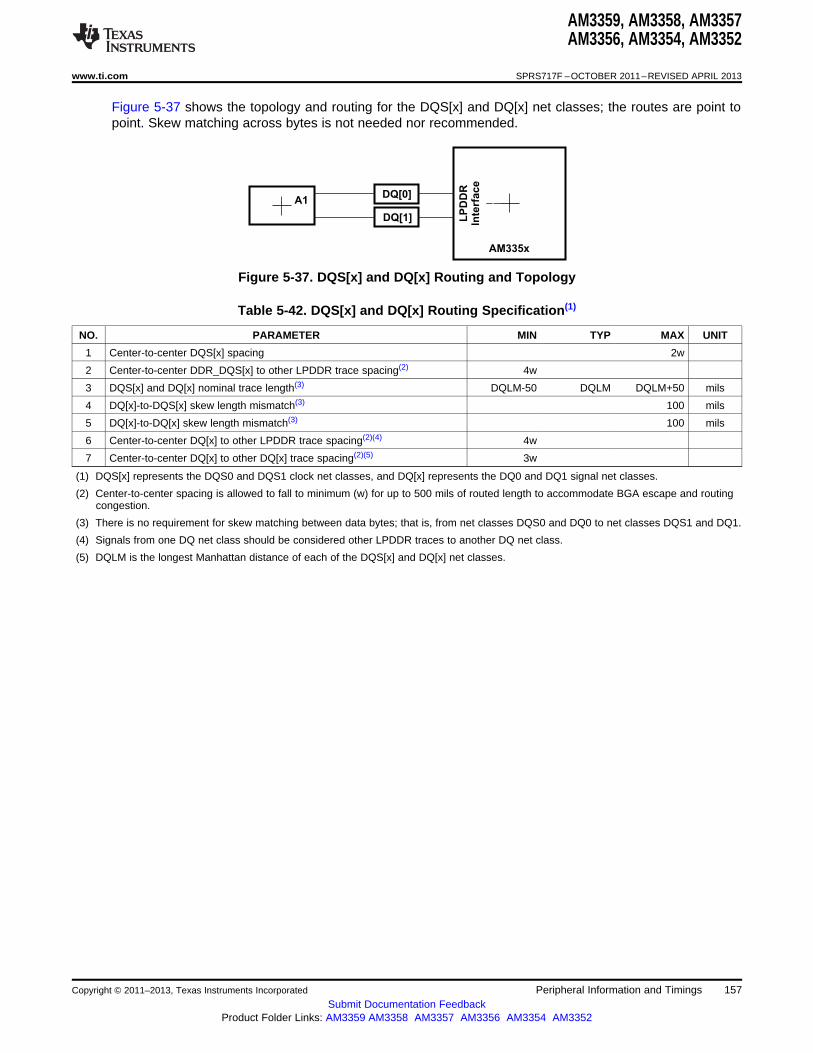
AM335x
LP
DD
RIn
terf
ac
e
A1DQ[0]
DQ[1]
AM3359, AM3358, AM3357AM3356, AM3354, AM3352
www.ti.com SPRS717F –OCTOBER 2011–REVISED APRIL 2013
Figure 5-37 shows the topology and routing for the DQS[x] and DQ[x] net classes; the routes are point topoint. Skew matching across bytes is not needed nor recommended.
Figure 5-37. DQS[x] and DQ[x] Routing and Topology
Table 5-42. DQS[x] and DQ[x] Routing Specification(1)
NO. PARAMETER MIN TYP MAX UNIT
1 Center-to-center DQS[x] spacing 2w
2 Center-to-center DDR_DQS[x] to other LPDDR trace spacing(2) 4w
3 DQS[x] and DQ[x] nominal trace length(3) DQLM-50 DQLM DQLM+50 mils
4 DQ[x]-to-DQS[x] skew length mismatch(3) 100 mils
5 DQ[x]-to-DQ[x] skew length mismatch(3) 100 mils
6 Center-to-center DQ[x] to other LPDDR trace spacing(2)(4) 4w
7 Center-to-center DQ[x] to other DQ[x] trace spacing(2)(5) 3w
(1) DQS[x] represents the DQS0 and DQS1 clock net classes, and DQ[x] represents the DQ0 and DQ1 signal net classes.
(2) Center-to-center spacing is allowed to fall to minimum (w) for up to 500 mils of routed length to accommodate BGA escape and routingcongestion.
(3) There is no requirement for skew matching between data bytes; that is, from net classes DQS0 and DQ0 to net classes DQS1 and DQ1.
(4) Signals from one DQ net class should be considered other LPDDR traces to another DQ net class.
(5) DQLM is the longest Manhattan distance of each of the DQS[x] and DQ[x] net classes.
Copyright © 2011–2013, Texas Instruments Incorporated Peripheral Information and Timings 157Submit Documentation Feedback
Product Folder Links: AM3359 AM3358 AM3357 AM3356 AM3354 AM3352

DDR_CK
1
DDR_CKn
AM3359, AM3358, AM3357AM3356, AM3354, AM3352
SPRS717F –OCTOBER 2011–REVISED APRIL 2013 www.ti.com
5.6.2.2 DDR2 Routing Guidelines
5.6.2.2.1 Board Designs
TI only supports board designs that follow the guidelines outlined in this document. The switchingcharacteristics and the timing diagram for the DDR2 memory interface are shown in Table 5-43 andFigure 5-38.
Table 5-43. Switching Characteristics for DDR2 Memory Interface
NO. PARAMETER MIN MAX UNIT
tc(DDR_CK)1 Cycle time, DDR_CK and DDR_CKn 3.75 8(1) nstc(DDR_CKn)
(1) The JEDEC JESD79-2F specification defines the maximum clock period of 8 ns for all standard-speed bin DDR2 memory devices.Therefore, all standard-speed bin DDR2 memory devices are required to operate at 125 MHz.
Figure 5-38. DDR2 Memory Interface Clock Timing
5.6.2.2.2 DDR2 Interface
This section provides the timing specification for the DDR2 interface as a PCB design and manufacturingspecification. The design rules constrain PCB trace length, PCB trace skew, signal integrity, cross-talk,and signal timing. These rules, when followed, result in a reliable DDR2 memory system without the needfor a complex timing closure process. For more information regarding the guidelines for using this DDR2specification, see the Understanding TI’s PCB Routing Rule-Based DDR Timing Specification applicationreport (literature number SPRAAV0). This application report provides generic guidelines and approach. Allthe specifications provided in the data manual take precedence over the generic guidelines and must beadhered to for a reliable DDR2 interface operation.
5.6.2.2.2.1 DDR2 Interface Schematic
Figure 5-39 shows the schematic connections for 16-bit interface on AM335x device using one x16 DDR2device and Figure 5-40 shows the schematic connections for 16-bit interface on AM335x using two x8DDR2 devices. The AM335x DDR2 memory interface only supports 16-bit wide mode of operation. TheAM335x device can only source one load connected to the DQS[x] and DQ[x] net class signals and twoloads connected to the CK and ADDR_CTRL net class signals. For more information related to netclasses, see Section 5.6.2.2.2.8.
158 Peripheral Information and Timings Copyright © 2011–2013, Texas Instruments Incorporated
Submit Documentation FeedbackProduct Folder Links: AM3359 AM3358 AM3357 AM3356 AM3354 AM3352
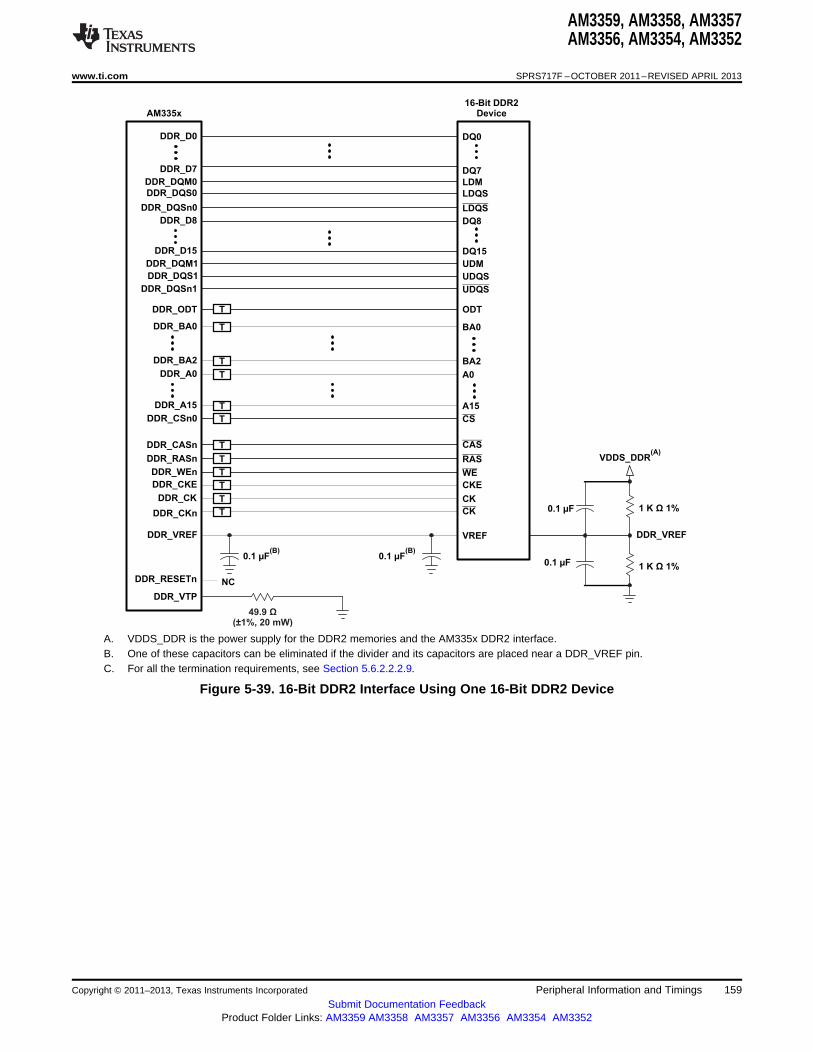
DDR_D0
DDR_D7
DDR_DQM0
DDR_DQS0
DDR_DQSn0
DDR_D8
DDR_D15
DDR_DQM1
DDR_DQS1
DDR_DQSn1
DQ0
DQ7
LDM
LDQS
LDQS
DQ8
DQ15
UDM
UDQS
UDQS
BA0
BA2
A0
A15
CS
CAS
RAS
WE
CKE
CK
CK
VREF
DDR_BA0
DDR_BA2
DDR_A0
DDR_A15
DDR_CSn0
DDR_CASn
DDR_RASn
DDR_WEn
DDR_CKE
DDR_CK
DDR_CKn
DDR_VREF
1 K Ω 1%
VDDS_DDR(A)
16-Bit DDR2Device
0.1 µF
0.1 µF 1 K Ω 1%0.1 µF
(B)0.1 µF
(B)
ODT
DDR_VTP
49.9( 1%, 20 mW)
Ω±
TDDR_ODT
DDR_RESETn NC
DDR_VREF
AM335x
T
T
T
T
T
T
T
T
T
T
T
AM3359, AM3358, AM3357AM3356, AM3354, AM3352
www.ti.com SPRS717F –OCTOBER 2011–REVISED APRIL 2013
A. VDDS_DDR is the power supply for the DDR2 memories and the AM335x DDR2 interface.B. One of these capacitors can be eliminated if the divider and its capacitors are placed near a DDR_VREF pin.C. For all the termination requirements, see Section 5.6.2.2.2.9.
Figure 5-39. 16-Bit DDR2 Interface Using One 16-Bit DDR2 Device
Copyright © 2011–2013, Texas Instruments Incorporated Peripheral Information and Timings 159Submit Documentation Feedback
Product Folder Links: AM3359 AM3358 AM3357 AM3356 AM3354 AM3352
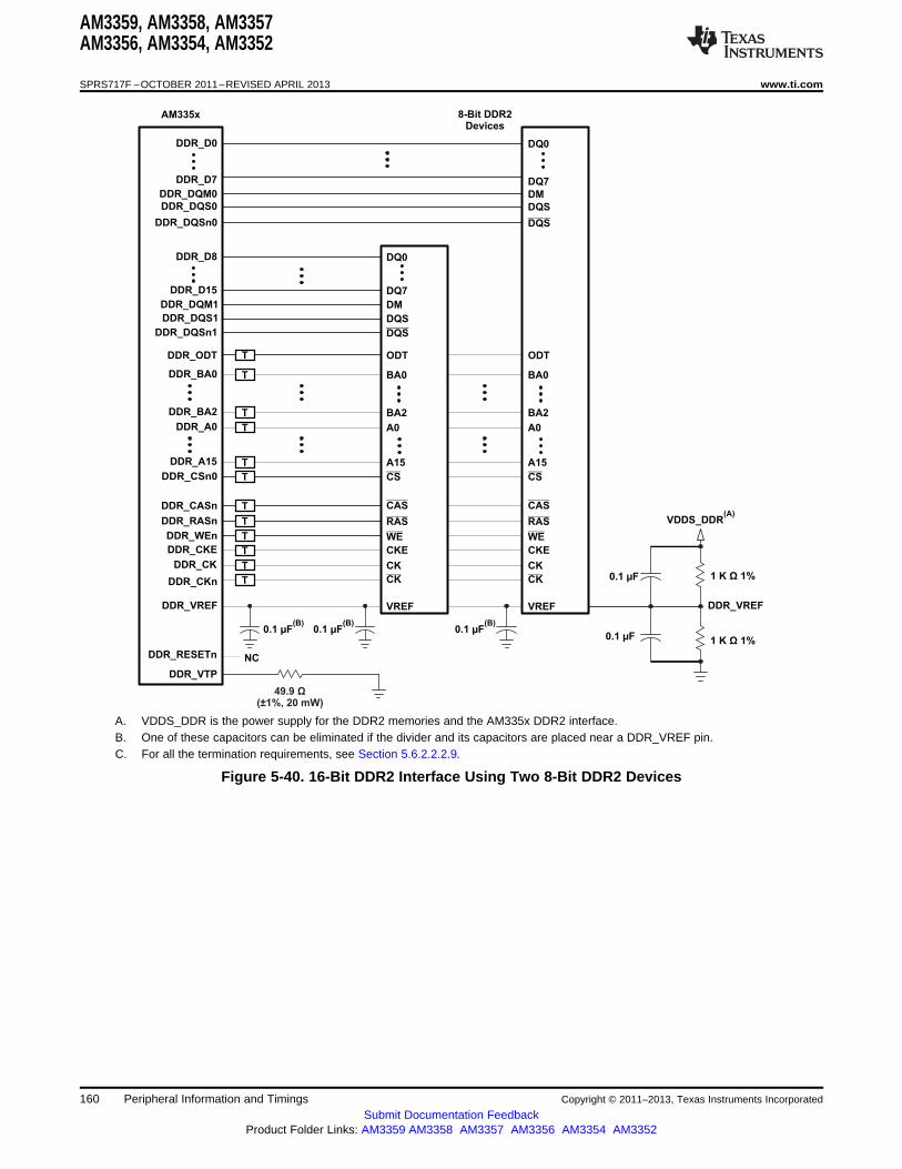
DDR_D0
DDR_D7
DDR_DQM0
DDR_DQS0
DDR_DQSn0
DDR_D8
DDR_D15
DDR_DQM1
DDR_DQS1
DDR_DQSn1
DQ0
DQ7
DM
DQS
DQS
BA0
BA2
A0
A15
CS
CAS
RAS
WE
CKE
CK
CK
VREF
DDR_BA0
DDR_BA2
DDR_A0
DDR_A15
DDR_CSn0
DDR_CASn
DDR_RASn
DDR_WEn
DDR_CKE
DDR_CK
DDR_CKn
DDR_VREF
1 K Ω 1%
VDDS_DDR(A)
8-Bit DDR2Devices
0.1 µF
0.1 µF 1 K Ω 1%0.1 µF
(B)0.1 µF
(B)
ODT
DDR_VTP
49.9( 1%, 20 mW)
Ω±
TDDR_ODT
DDR_RESETn NC
DDR_VREF
AM335x
T
T
T
T
T
T
T
T
T
T
T
DQ0
DQ7
DM
DQS
DQS
BA0
BA2
A0
A15
CS
CAS
RAS
WE
CKE
CK
CK
VREF
ODT
0.1 µF(B)
AM3359, AM3358, AM3357AM3356, AM3354, AM3352
SPRS717F –OCTOBER 2011–REVISED APRIL 2013 www.ti.com
A. VDDS_DDR is the power supply for the DDR2 memories and the AM335x DDR2 interface.B. One of these capacitors can be eliminated if the divider and its capacitors are placed near a DDR_VREF pin.C. For all the termination requirements, see Section 5.6.2.2.2.9.
Figure 5-40. 16-Bit DDR2 Interface Using Two 8-Bit DDR2 Devices
160 Peripheral Information and Timings Copyright © 2011–2013, Texas Instruments Incorporated
Submit Documentation FeedbackProduct Folder Links: AM3359 AM3358 AM3357 AM3356 AM3354 AM3352
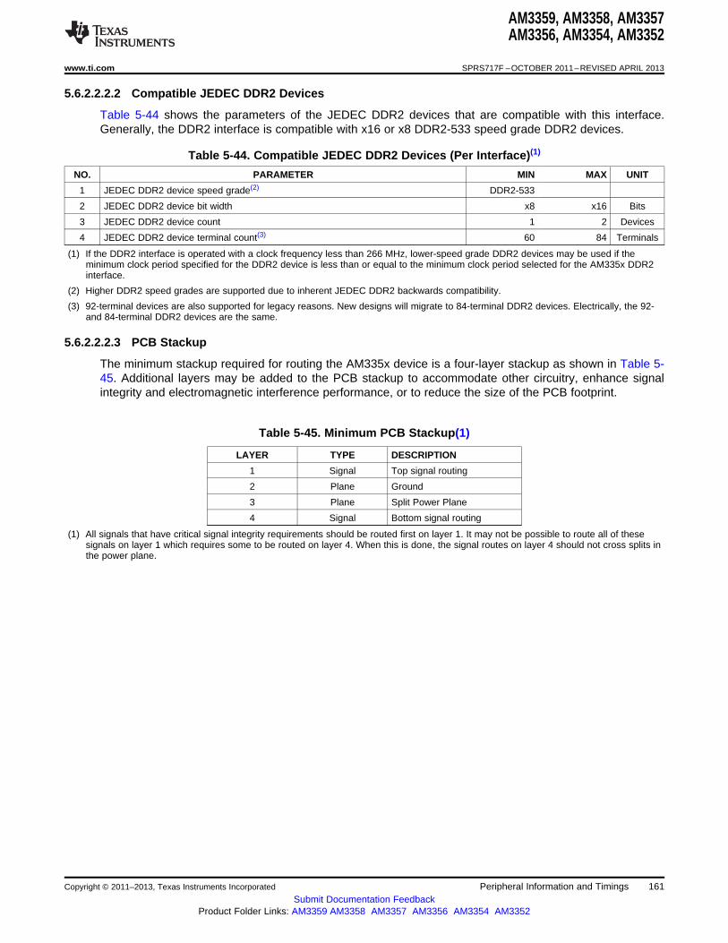
AM3359, AM3358, AM3357AM3356, AM3354, AM3352
www.ti.com SPRS717F –OCTOBER 2011–REVISED APRIL 2013
5.6.2.2.2.2 Compatible JEDEC DDR2 Devices
Table 5-44 shows the parameters of the JEDEC DDR2 devices that are compatible with this interface.Generally, the DDR2 interface is compatible with x16 or x8 DDR2-533 speed grade DDR2 devices.
Table 5-44. Compatible JEDEC DDR2 Devices (Per Interface)(1)
NO. PARAMETER MIN MAX UNIT
1 JEDEC DDR2 device speed grade(2) DDR2-533
2 JEDEC DDR2 device bit width x8 x16 Bits
3 JEDEC DDR2 device count 1 2 Devices
4 JEDEC DDR2 device terminal count(3) 60 84 Terminals
(1) If the DDR2 interface is operated with a clock frequency less than 266 MHz, lower-speed grade DDR2 devices may be used if theminimum clock period specified for the DDR2 device is less than or equal to the minimum clock period selected for the AM335x DDR2interface.
(2) Higher DDR2 speed grades are supported due to inherent JEDEC DDR2 backwards compatibility.
(3) 92-terminal devices are also supported for legacy reasons. New designs will migrate to 84-terminal DDR2 devices. Electrically, the 92-and 84-terminal DDR2 devices are the same.
5.6.2.2.2.3 PCB Stackup
The minimum stackup required for routing the AM335x device is a four-layer stackup as shown in Table 5-45. Additional layers may be added to the PCB stackup to accommodate other circuitry, enhance signalintegrity and electromagnetic interference performance, or to reduce the size of the PCB footprint.
Table 5-45. Minimum PCB Stackup(1)
LAYER TYPE DESCRIPTION
1 Signal Top signal routing
2 Plane Ground
3 Plane Split Power Plane
4 Signal Bottom signal routing
(1) All signals that have critical signal integrity requirements should be routed first on layer 1. It may not be possible to route all of thesesignals on layer 1 which requires some to be routed on layer 4. When this is done, the signal routes on layer 4 should not cross splits inthe power plane.
Copyright © 2011–2013, Texas Instruments Incorporated Peripheral Information and Timings 161Submit Documentation Feedback
Product Folder Links: AM3359 AM3358 AM3357 AM3356 AM3354 AM3352
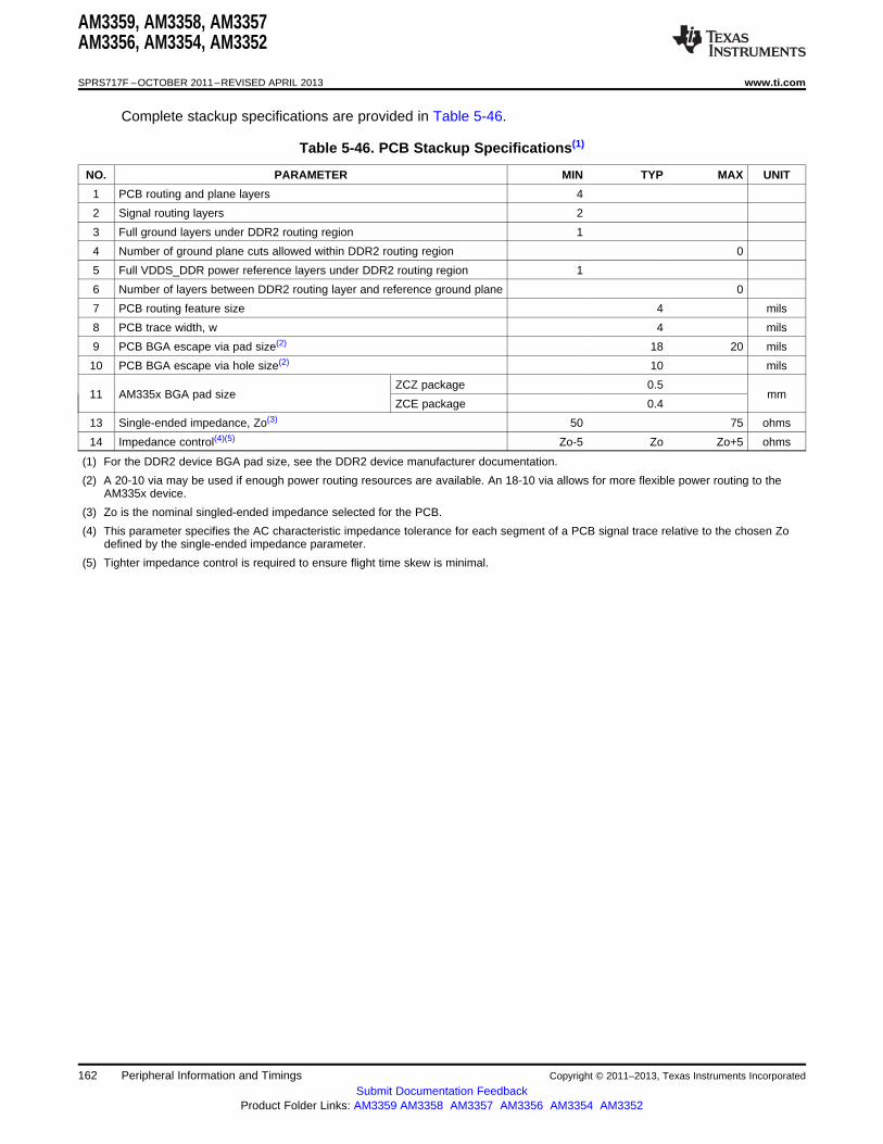
AM3359, AM3358, AM3357AM3356, AM3354, AM3352
SPRS717F –OCTOBER 2011–REVISED APRIL 2013 www.ti.com
Complete stackup specifications are provided in Table 5-46.
Table 5-46. PCB Stackup Specifications(1)
NO. PARAMETER MIN TYP MAX UNIT
1 PCB routing and plane layers 4
2 Signal routing layers 2
3 Full ground layers under DDR2 routing region 1
4 Number of ground plane cuts allowed within DDR2 routing region 0
5 Full VDDS_DDR power reference layers under DDR2 routing region 1
6 Number of layers between DDR2 routing layer and reference ground plane 0
7 PCB routing feature size 4 mils
8 PCB trace width, w 4 mils
9 PCB BGA escape via pad size(2) 18 20 mils
10 PCB BGA escape via hole size(2) 10 mils
ZCZ package 0.511 AM335x BGA pad size mm
ZCE package 0.4
13 Single-ended impedance, Zo(3) 50 75 ohms
14 Impedance control(4)(5) Zo-5 Zo Zo+5 ohms
(1) For the DDR2 device BGA pad size, see the DDR2 device manufacturer documentation.
(2) A 20-10 via may be used if enough power routing resources are available. An 18-10 via allows for more flexible power routing to theAM335x device.
(3) Zo is the nominal singled-ended impedance selected for the PCB.
(4) This parameter specifies the AC characteristic impedance tolerance for each segment of a PCB signal trace relative to the chosen Zodefined by the single-ended impedance parameter.
(5) Tighter impedance control is required to ensure flight time skew is minimal.
162 Peripheral Information and Timings Copyright © 2011–2013, Texas Instruments Incorporated
Submit Documentation FeedbackProduct Folder Links: AM3359 AM3358 AM3357 AM3356 AM3354 AM3352
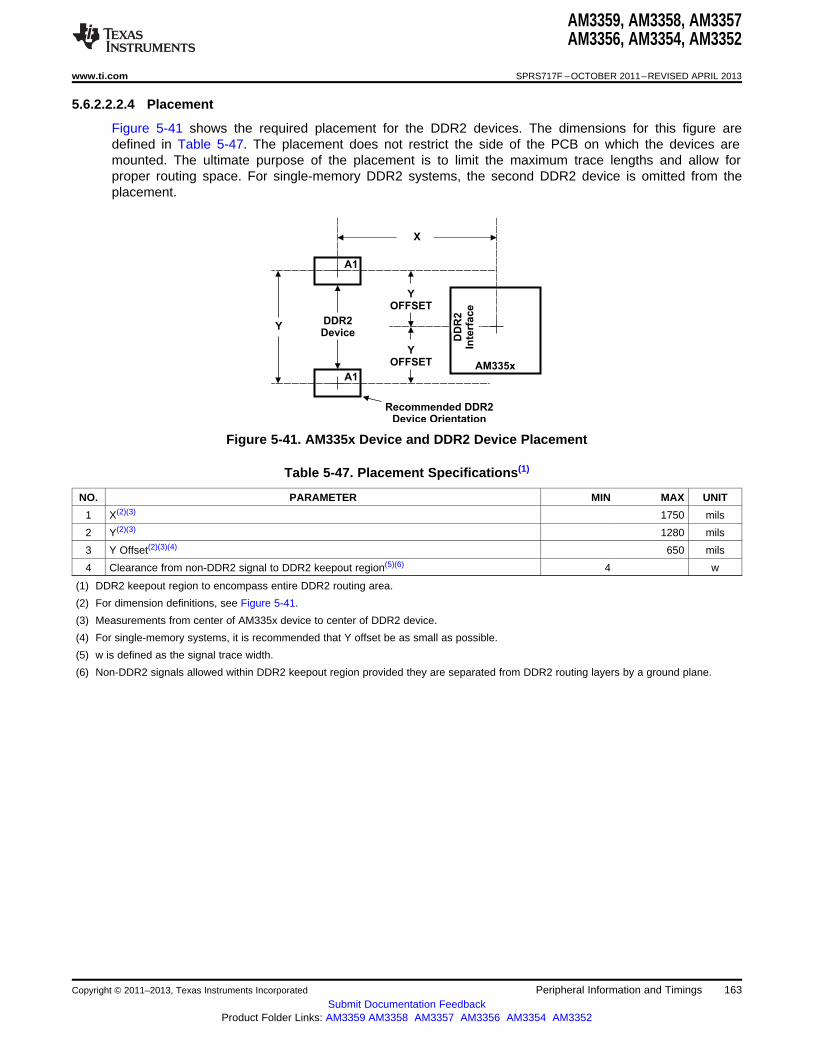
A1
A1
X
Y
OFFSET
Recommended DDR2
Device Orientation
Y
Y
OFFSET
DDR2
Device
DD
R2
Inte
rfa
ce
AM335x
AM3359, AM3358, AM3357AM3356, AM3354, AM3352
www.ti.com SPRS717F –OCTOBER 2011–REVISED APRIL 2013
5.6.2.2.2.4 Placement
Figure 5-41 shows the required placement for the DDR2 devices. The dimensions for this figure aredefined in Table 5-47. The placement does not restrict the side of the PCB on which the devices aremounted. The ultimate purpose of the placement is to limit the maximum trace lengths and allow forproper routing space. For single-memory DDR2 systems, the second DDR2 device is omitted from theplacement.
Figure 5-41. AM335x Device and DDR2 Device Placement
Table 5-47. Placement Specifications(1)
NO. PARAMETER MIN MAX UNIT
1 X(2)(3) 1750 mils
2 Y(2)(3) 1280 mils
3 Y Offset(2)(3)(4) 650 mils
4 Clearance from non-DDR2 signal to DDR2 keepout region(5)(6) 4 w
(1) DDR2 keepout region to encompass entire DDR2 routing area.
(2) For dimension definitions, see Figure 5-41.
(3) Measurements from center of AM335x device to center of DDR2 device.
(4) For single-memory systems, it is recommended that Y offset be as small as possible.
(5) w is defined as the signal trace width.
(6) Non-DDR2 signals allowed within DDR2 keepout region provided they are separated from DDR2 routing layers by a ground plane.
Copyright © 2011–2013, Texas Instruments Incorporated Peripheral Information and Timings 163Submit Documentation Feedback
Product Folder Links: AM3359 AM3358 AM3357 AM3356 AM3354 AM3352

A1
A1
DD
R2
Inte
rfa
ce
DDR2Device
AM3359, AM3358, AM3357AM3356, AM3354, AM3352
SPRS717F –OCTOBER 2011–REVISED APRIL 2013 www.ti.com
5.6.2.2.2.5 DDR2 Keepout Region
The region of the PCB used for the DDR2 circuitry must be isolated from other signals. The DDR2keepout region is defined for this purpose and is shown in Figure 5-42. This region should encompass allDDR2 circuitry and the region size varies with component placement and DDR2 routing. Additionalclearances required for the keepout region are shown in Table 5-47. Non-DDR2 signals should not berouted on the same signal layer as DDR2 signals within the DDR2 keepout region. Non-DDR2 signalsmay be routed in the region provided they are routed on layers separated from DDR2 signal layers by aground layer. No breaks should be allowed in the reference ground or VDDS_DDR power plane in thisregion. In addition, the VDDS_DDR power plane should cover the entire keepout region.
Figure 5-42. DDR2 Keepout Region
5.6.2.2.2.6 Bulk Bypass Capacitors
Bulk bypass capacitors are required for moderate speed bypassing of the DDR2 and other circuitry.Table 5-48 contains the minimum numbers and capacitance required for the bulk bypass capacitors. Notethat this table only covers the bypass needs of the AM335x DDR2 interface and DDR2 devices. Additionalbulk bypass capacitance may be needed for other circuitry.
Table 5-48. Bulk Bypass Capacitors(1)
NO. PARAMETER MIN MAX UNIT
1 AM335x VDDS_DDR bulk bypass capacitor count 1 Devices
2 AM335x VDDS_DDR bulk bypass total capacitance 10 μF
3 DDR2#1 bulk bypass capacitor count 1 Devices
4 DDR2#1 bulk bypass total capacitance 10 μF
5 DDR2#2 bulk bypass capacitor count(2) 1 Devices
6 DDR2#2 bulk bypass total capacitance(2) 10 μF
(1) These devices should be placed near the device they are bypassing, but preference should be given to the placement of the high-speed(HS) bypass capacitors.
(2) Only used when two DDR2 devices are used.
164 Peripheral Information and Timings Copyright © 2011–2013, Texas Instruments Incorporated
Submit Documentation FeedbackProduct Folder Links: AM3359 AM3358 AM3357 AM3356 AM3354 AM3352
AM3359, AM3358, AM3357AM3356, AM3354, AM3352
www.ti.com SPRS717F –OCTOBER 2011–REVISED APRIL 2013
5.6.2.2.2.7 High-Speed Bypass Capacitors
High-speed (HS) bypass capacitors are critical for proper DDR2 interface operation. It is particularlyimportant to minimize the parasitic series inductance of the HS bypass capacitors, AM335x device DDR2power, and AM335x device DDR2 ground connections. Table 5-49 contains the specification for the HSbypass capacitors as well as for the power connections on the PCB.
Table 5-49. High-Speed Bypass Capacitors
NO. PARAMETER MIN MAX UNIT
1 HS bypass capacitor package size(1) 0402 10 mils
2 Distance from HS bypass capacitor to device being bypassed 250 mils
3 Number of connection vias for each HS bypass capacitor(2) 2 Vias
4 Trace length from bypass capacitor contact to connection via 30 mils
5 Number of connection vias for each AM335x VDDS_DDR and VSS terminal 1 Vias
6 Trace length from AM335x VDDS_DDR and VSS terminal to connection via 35 mils
7 Number of connection vias for each DDR2 device power and ground terminal 1 Vias
8 Trace length from DDR2 device power and ground terminal to connection via 35 mils
9 AM335x VDDS_DDR HS bypass capacitor count(3) 10 Devices
10 AM335x VDDS_DDR HS bypass capacitor total capacitance 0.6 μF
11 DDR2 device HS bypass capacitor count(3)(4) 8 Devices
12 DDR2 device HS bypass capacitor total capacitance(4) 0.4 μF
(1) LxW, 10-mil units; for example, a 0402 is a 40x20-mil surface-mount capacitor.
(2) An additional HS bypass capacitor can share the connection vias only if it is mounted on the opposite side of the board.
(3) These devices should be placed as close as possible to the device being bypassed.
(4) Per DDR2 device.
5.6.2.2.2.8 Net Classes
Table 5-50 lists the clock net classes for the DDR2 interface. Table 5-51 lists the signal net classes, andassociated clock net classes, for the signals in the DDR2 interface. These net classes are used for thetermination and routing rules that follow.
Table 5-50. Clock Net Class Definitions
CLOCK NET CLASS AM335x PIN NAMES
CK DDR_CK and DDR_CKn
DQS0 DDR_DQS0 and DDR_DQSn0
DQS1 DDR_DQS1 and DDR_DQSn1
Table 5-51. Signal Net Class Definitions
ASSOCIATED CLOCKSIGNAL NET CLASS AM335x PIN NAMESNET CLASS
ADDR_CTRL CK DDR_BA[2:0], DDR_A[15:0], DDR_CSn0, DDR_CASn, DDR_RASn,DDR_WEn, DDR_CKE, DDR_ODT
DQ0 DQS0 DDR_D[7:0], DDR_DQM0
DQ1 DQS1 DDR_D[15:8], DDR_DQM1
Copyright © 2011–2013, Texas Instruments Incorporated Peripheral Information and Timings 165Submit Documentation Feedback
Product Folder Links: AM3359 AM3358 AM3357 AM3356 AM3354 AM3352
AM3359, AM3358, AM3357AM3356, AM3354, AM3352
SPRS717F –OCTOBER 2011–REVISED APRIL 2013 www.ti.com
5.6.2.2.2.9 DDR2 Signal Termination
Signal terminations are required on the CK and ADDR_CTRL net class signals. Serial terminations shouldbe used on the CK and ADDR_CTRL lines and is the preferred termination scheme. On-deviceterminations (ODTs) are required on the DQS[x] and DQ[x] net class signals. They should be enabled toensure signal integrity. Table 5-52 shows the specifications for the series terminators. Placement of serialterminations for ADDR_CTRL net class signals should be close to the AM335x device.
Table 5-52. DDR2 Signal Terminations
NO. PARAMETER MIN TYP MAX UNIT
1 CK net class(1) 0 10 ohms
2 ADDR_CTRL net class(1)(2)(3) 0 22 Zo(4) ohms
3 DQS0, DQS1, DQ0, and DQ1 net classes(5) NA NA ohms
(1) Only series termination is permitted.
(2) Series termination values larger than typical only recommended to address EMI issues.
(3) Series termination values should be uniform across net class.
(4) Zo is the DDR2 PCB trace characteristic impedance.
(5) No external termination resistors are allowed and ODT must be used for these net classes.
If the DDR2 interface is operated at a lower frequency (<200-MHz clock rate), on-device terminations arenot specifically required for the DQS[x] and DQ[x] net class signals and serial terminations for the CK andADDR_CTRL net class signals are not mandatory. System designers may evaluate the need for serialterminators for EMI and overshoot reduction. Placement of serial terminations for DQS[x] and DQ[x] netclass signals should be determined based on PCB analysis. Placement of serial terminations forADDR_CTRL net class signals should be close to the AM335x device. Table 5-53 shows thespecifications for the serial terminators in such cases.
Table 5-53. Lower-Frequency DDR2 Signal Terminations
NO. PARAMETER MIN TYP MAX UNIT
1 CK net class(1) 0 22 Zo(2) ohms
2 ADDR_CTRL net class(1)(3)(4) 0 22 Zo(2) ohms
3 DQS0, DQS1, DQ0, and DQ1 net classes 0 22 Zo(2) ohms
(1) Only series termination is permitted.
(2) Zo is the DDR2 PCB trace characteristic impedance.
(3) Series termination values larger than typical only recommended to address EMI issues.
(4) Series termination values should be uniform across net class.
166 Peripheral Information and Timings Copyright © 2011–2013, Texas Instruments Incorporated
Submit Documentation FeedbackProduct Folder Links: AM3359 AM3358 AM3357 AM3356 AM3354 AM3352

AM335x
A1
A1
DDR2 Device
DDR_VREF Nominal MinimumTrace Width is 20 Mils
DDR_VREF Bypass Capacitor
Neck down to minimum in BGA escaperegions is acceptable. Narrowing toaccommodate via congestion for shortdistances is also acceptable. Bestperformance is obtained if the widthof DDR_VREF is maximized.
AM3359, AM3358, AM3357AM3356, AM3354, AM3352
www.ti.com SPRS717F –OCTOBER 2011–REVISED APRIL 2013
5.6.2.2.2.10 DDR_VREF Routing
DDR_VREF is used as a reference by the input buffers of the DDR2 memories as well as the AM335xdevice. DDR_VREF is intended to be half the DDR2 power supply voltage and should be created using aresistive divider as shown in Figure 5-39 and Figure 5-40. Other methods of creating DDR_VREF are notrecommended. Figure 5-43 shows the layout guidelines for DDR_VREF.
Figure 5-43. DDR_VREF Routing and Topology
Copyright © 2011–2013, Texas Instruments Incorporated Peripheral Information and Timings 167Submit Documentation Feedback
Product Folder Links: AM3359 AM3358 AM3357 AM3356 AM3354 AM3352

AM335x
DD
R2
Inte
rfa
ce
A1DQ[0]
DQ[1]
A1
A1
CB
A
T
DD
R2
Inte
rfa
ce
AM335x
AM3359, AM3358, AM3357AM3356, AM3354, AM3352
SPRS717F –OCTOBER 2011–REVISED APRIL 2013 www.ti.com
5.6.2.2.3 DDR2 CK and ADDR_CTRL Routing
Figure 5-44 shows the topology of the routing for the CK and ADDR_CTRL net classes. The length ofsignal path AB and AC should be minimized with emphasis to minimize lengths C and D such that lengthA is the majority of the total length of signal path AB and AC.
Figure 5-44. CK and ADDR_CTRL Routing and Topology
Table 5-54. CK and ADDR_CTRL Routing Specification(1)(2)
NO. PARAMETER MIN TYP MAX UNIT
1 Center-to-center CK spacing 2w
2 CK differential pair skew length mismatch(2)(3) 25 mils
3 CK B-to-CK C skew length mismatch 25 mils
4 Center-to-center CK to other DDR2 trace spacing(4) 4w
5 CK and ADDR_CTRL nominal trace length(5) CACLM-50 CACLM CACLM+50 mils
6 ADDR_CTRL-to-CK skew length mismatch 100 mils
7 ADDR_CTRL-to-ADDR_CTRL skew length mismatch 100 mils
8 Center-to-center ADDR_CTRL to other DDR2 trace spacing(4) 4w
9 Center-to-center ADDR_CTRL to other ADDR_CTRL trace spacing(4) 3w
10 ADDR_CTRL A-to-B and ADDR_CTRL A-to-C skew length mismatch(2) 100 mils
11 ADDR_CTRL B-to-C skew length mismatch 100 mils
(1) CK represents the clock net class, and ADDR_CTRL represents the address and control signal net class.
(2) Series terminator, if used, should be located closest to the AM335x device.
(3) Differential impedance should be Zo x 2, where Zo is the single-ended impedance defined in Table 5-46.
(4) Center-to-center spacing is allowed to fall to minimum (w) for up to 500 mils of routed length to accommodate BGA escape and routingcongestion.
(5) CACLM is the longest Manhattan distance of the CK and ADDR_CTRL net classes.
Figure 5-45 shows the topology and routing for the DQS[x] and DQ[x] net classes; the routes are point topoint. Skew matching across bytes is not needed nor recommended.
Figure 5-45. DQS[x] and DQ[x] Routing and Topology
168 Peripheral Information and Timings Copyright © 2011–2013, Texas Instruments Incorporated
Submit Documentation FeedbackProduct Folder Links: AM3359 AM3358 AM3357 AM3356 AM3354 AM3352
AM3359, AM3358, AM3357AM3356, AM3354, AM3352
www.ti.com SPRS717F –OCTOBER 2011–REVISED APRIL 2013
Table 5-55. DQS[x] and DQ[x] Routing Specification(1)
NO. PARAMETER MIN TYP MAX UNIT
1 Center-to-center DQS[x] spacing 2w
2 DQS[x] differential pair skew length mismatch(2) 25 mils
3 Center-to-center DDR_DQS[x] to other DDR2 trace spacing(3) 4w
4 DQS[x] and DQ[x] nominal trace length(4) DQLM-50 DQLM DQLM+50 mils
5 DQ[x]-to-DQS[x] skew length mismatch(4) 100 mils
6 DQ[x]-to-DQ[x] skew length mismatch(4) 100 mils
7 Center-to-center DQ[x] to other DDR2 trace spacing(3)(5) 4w
8 Center-to-center DQ[x] to other DQ[x] trace spacing(3)(6) 3w
(1) DQS[x] represents the DQS0 and DQS1 clock net classes, and DQ[x] represents the DQ0 and DQ1 signal net classes.
(2) Differential impedance should be Zo x 2, where Zo is the single-ended impedance defined in Table 5-46.
(3) Center-to-center spacing is allowed to fall to minimum (w) for up to 500 mils of routed length to accommodate BGA escape and routingcongestion.
(4) There is no requirement for skew matching between data bytes; that is, from net classes DQS0 and DQ0 to net classes DQS1 and DQ1.
(5) Signals from one DQ net class should be considered other DDR2 traces to another DQ net class.
(6) DQLM is the longest Manhattan distance of each of the DQS[x] and DQ[x] net classes.
Copyright © 2011–2013, Texas Instruments Incorporated Peripheral Information and Timings 169Submit Documentation Feedback
Product Folder Links: AM3359 AM3358 AM3357 AM3356 AM3354 AM3352
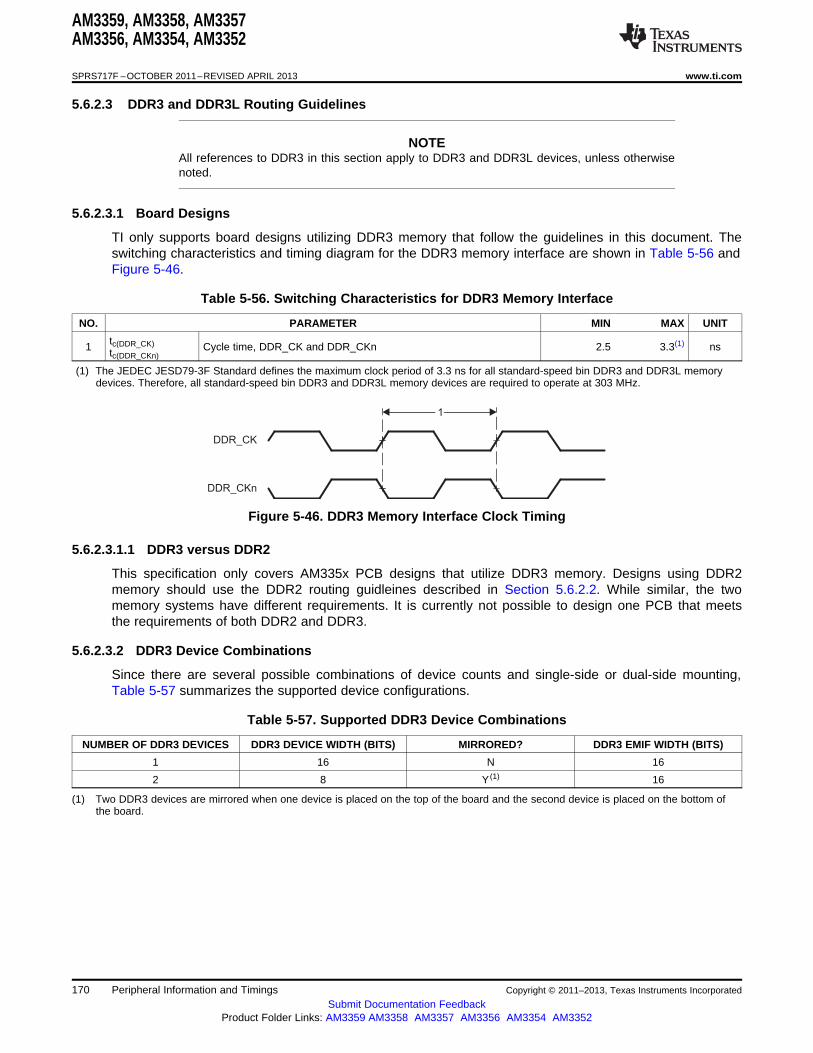
DDR_CK
1
DDR_CKn
AM3359, AM3358, AM3357AM3356, AM3354, AM3352
SPRS717F –OCTOBER 2011–REVISED APRIL 2013 www.ti.com
5.6.2.3 DDR3 and DDR3L Routing Guidelines
NOTEAll references to DDR3 in this section apply to DDR3 and DDR3L devices, unless otherwisenoted.
5.6.2.3.1 Board Designs
TI only supports board designs utilizing DDR3 memory that follow the guidelines in this document. Theswitching characteristics and timing diagram for the DDR3 memory interface are shown in Table 5-56 andFigure 5-46.
Table 5-56. Switching Characteristics for DDR3 Memory Interface
NO. PARAMETER MIN MAX UNIT
tc(DDR_CK)1 Cycle time, DDR_CK and DDR_CKn 2.5 3.3(1) nstc(DDR_CKn)
(1) The JEDEC JESD79-3F Standard defines the maximum clock period of 3.3 ns for all standard-speed bin DDR3 and DDR3L memorydevices. Therefore, all standard-speed bin DDR3 and DDR3L memory devices are required to operate at 303 MHz.
Figure 5-46. DDR3 Memory Interface Clock Timing
5.6.2.3.1.1 DDR3 versus DDR2
This specification only covers AM335x PCB designs that utilize DDR3 memory. Designs using DDR2memory should use the DDR2 routing guidleines described in Section 5.6.2.2. While similar, the twomemory systems have different requirements. It is currently not possible to design one PCB that meetsthe requirements of both DDR2 and DDR3.
5.6.2.3.2 DDR3 Device Combinations
Since there are several possible combinations of device counts and single-side or dual-side mounting,Table 5-57 summarizes the supported device configurations.
Table 5-57. Supported DDR3 Device Combinations
NUMBER OF DDR3 DEVICES DDR3 DEVICE WIDTH (BITS) MIRRORED? DDR3 EMIF WIDTH (BITS)
1 16 N 16
2 8 Y (1) 16
(1) Two DDR3 devices are mirrored when one device is placed on the top of the board and the second device is placed on the bottom ofthe board.
170 Peripheral Information and Timings Copyright © 2011–2013, Texas Instruments Incorporated
Submit Documentation FeedbackProduct Folder Links: AM3359 AM3358 AM3357 AM3356 AM3354 AM3352
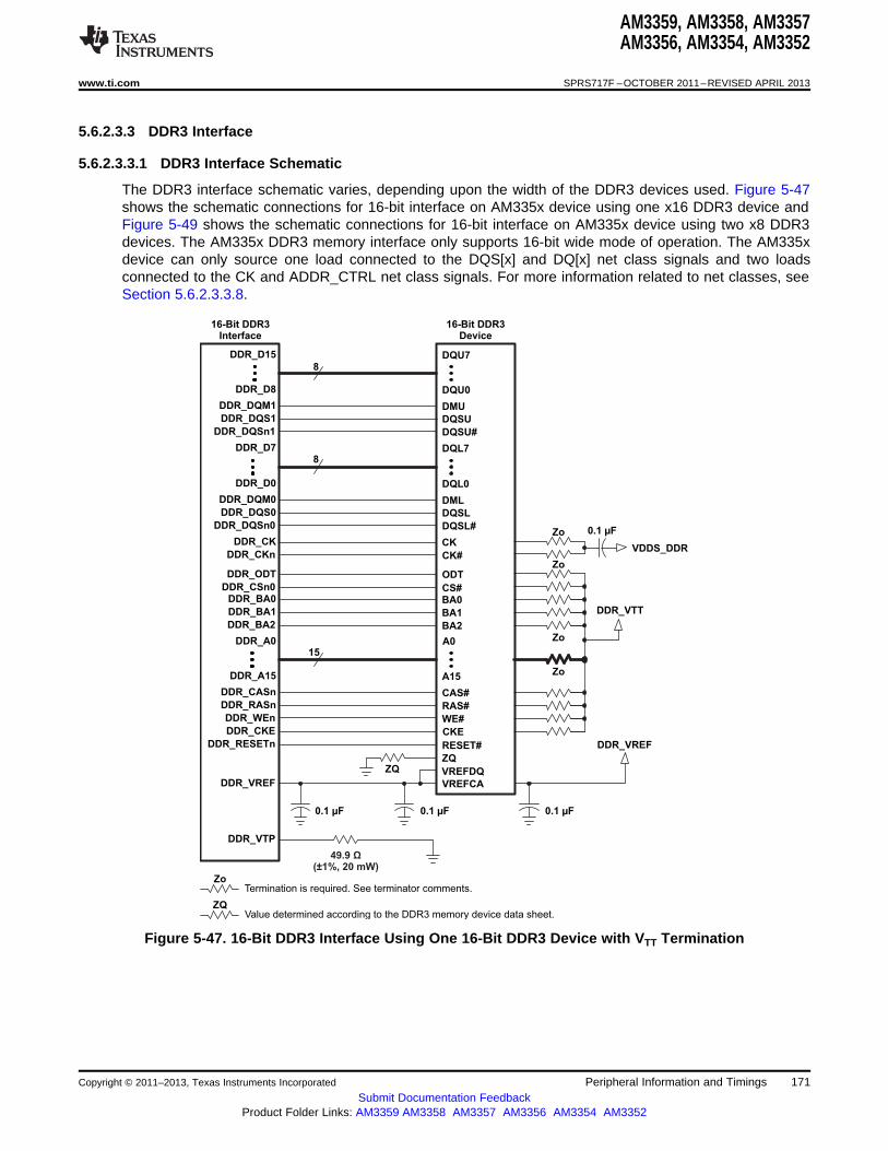
DQU7
DQU0
DMU
DQSU
DQSU#
DQL7
DQL0
DML
DQSL
DQSL#
CK#
16-Bit DDR3Device
0.1 µF
49.91 , 20 mW
Ω(± % )
0.1 µF 0.1 µF
16-Bit DDR3Interface
DDR_D15
DDR_D8
DDR_DQM1
DDR_DQS1
DDR_DQSn1
DDR_D7
DDR_D0
DDR_DQM0
DDR_DQS0
DDR_DQSn0
DDR_CK
DDR_CKn
DDR_ODT
DDR_CSn0DDR_BA0
DDR_BA1
DDR_BA2
DDR_A0
DDR_A15
DDR_CASn
DDR_RASn
DDR_WEn
DDR_CKE
DDR_RESETn
DDR_VREF
DDR_VTP
8
8
15
CK
ODT
BA1
BA0
BA2
CS#
A0
A15
CAS#
RAS#
WE#
RESET#
CKE
ZQ
VREFDQ
VREFCA
ZQ
Zo
Zo
Zo
Zo
DDR_VREF
DDR_VTT
VDDS_DDR
Termination is required. See terminator comments.Zo
Value determined according to the DDR3 memory device data sheet.ZQ
0.1 µF
AM3359, AM3358, AM3357AM3356, AM3354, AM3352
www.ti.com SPRS717F –OCTOBER 2011–REVISED APRIL 2013
5.6.2.3.3 DDR3 Interface
5.6.2.3.3.1 DDR3 Interface Schematic
The DDR3 interface schematic varies, depending upon the width of the DDR3 devices used. Figure 5-47shows the schematic connections for 16-bit interface on AM335x device using one x16 DDR3 device andFigure 5-49 shows the schematic connections for 16-bit interface on AM335x device using two x8 DDR3devices. The AM335x DDR3 memory interface only supports 16-bit wide mode of operation. The AM335xdevice can only source one load connected to the DQS[x] and DQ[x] net class signals and two loadsconnected to the CK and ADDR_CTRL net class signals. For more information related to net classes, seeSection 5.6.2.3.3.8.
Figure 5-47. 16-Bit DDR3 Interface Using One 16-Bit DDR3 Device with VTT Termination
Copyright © 2011–2013, Texas Instruments Incorporated Peripheral Information and Timings 171Submit Documentation Feedback
Product Folder Links: AM3359 AM3358 AM3357 AM3356 AM3354 AM3352
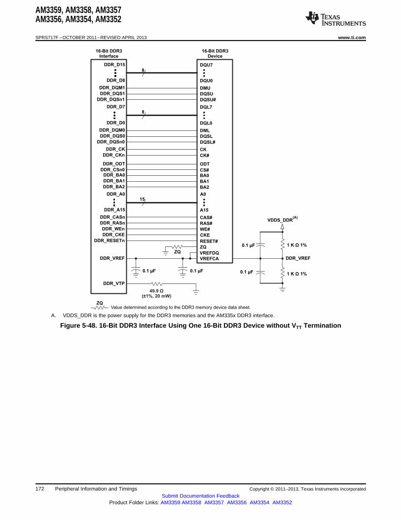
DQU7
DQU0
DMU
DQSU
DQSU#
DQL7
DQL0
DML
DQSL
DQSL#
CK#
16-Bit DDR3Device
0.1 µF
49.91 , 20 mW
Ω(± % )
0.1 µF
16-Bit DDR3Interface
DDR_D15
DDR_D8
DDR_DQM1
DDR_DQS1
DDR_DQSn1
DDR_D7
DDR_D0
DDR_DQM0
DDR_DQS0
DDR_DQSn0
DDR_CK
DDR_CKn
DDR_ODT
DDR_CSn0DDR_BA0
DDR_BA1
DDR_BA2
DDR_A0
DDR_A15
DDR_CASn
DDR_RASn
DDR_WEn
DDR_CKE
DDR_RESETn
DDR_VREF
DDR_VTP
8
8
15
CK
ODT
BA1
BA0
BA2
CS#
A0
A15
CAS#
RAS#
WE#
RESET#
CKE
ZQ
VREFDQ
VREFCA
ZQ
Value determined according to the DDR3 memory device data sheet.ZQ
1 K Ω 1%
VDDS_DDR(A)
0.1 µF
0.1 µF 1 K Ω 1%
DDR_VREF
AM3359, AM3358, AM3357AM3356, AM3354, AM3352
SPRS717F –OCTOBER 2011–REVISED APRIL 2013 www.ti.com
A. VDDS_DDR is the power supply for the DDR3 memories and the AM335x DDR3 interface.
Figure 5-48. 16-Bit DDR3 Interface Using One 16-Bit DDR3 Device without VTT Termination
172 Peripheral Information and Timings Copyright © 2011–2013, Texas Instruments Incorporated
Submit Documentation FeedbackProduct Folder Links: AM3359 AM3358 AM3357 AM3356 AM3354 AM3352
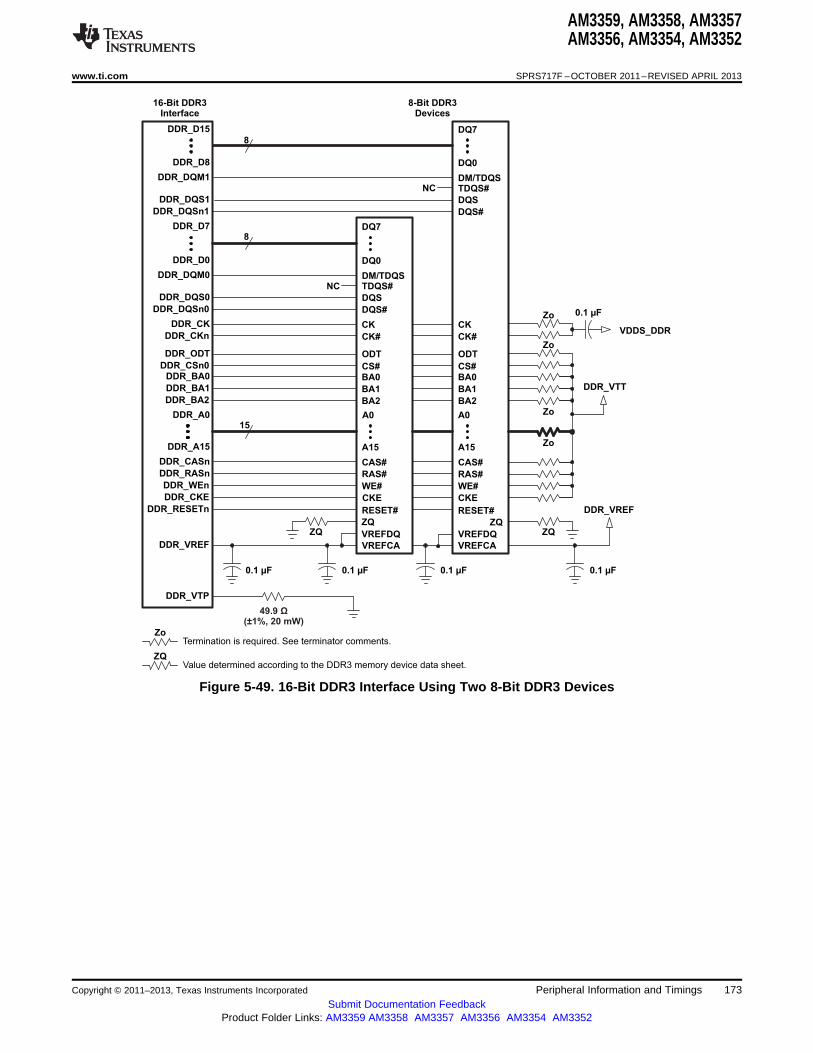
DQ7
DQ0
DQS
DQS#
DQ7
DQ0
DQS
DQS#
CK#
8-Bit DDR3Devices
0.1 µF
49.91 , 20 mW
Ω(± % )
0.1 µF 0.1 µF
16-Bit DDR3Interface
DDR_D15
DDR_D8
DDR_DQS1
DDR_DQSn1
DDR_D7
DDR_D0
DDR_DQS0
DDR_DQSn0
DDR_CK
DDR_CKn
DDR_ODT
DDR_CSn0DDR_BA0
DDR_BA1
DDR_BA2
DDR_A0
DDR_A15
DDR_CASn
DDR_RASn
DDR_WEn
DDR_CKE
DDR_RESETn
DDR_VREF
DDR_VTP
8
8
15
CK
ODT
BA1
BA0
BA2
CS#
A0
A15
CAS#
RAS#
WE#
RESET#
CKE
ZQ
VREFDQ
VREFCA
ZQ
CK#
CK
ODT
BA1
BA0
BA2
CS#
A0
A15
CAS#
RAS#
WE#
RESET#
CKE
ZQ
VREFDQ
VREFCA
Termination is required. See terminator comments.Zo
Value determined according to the DDR3 memory device data sheet.ZQ
0.1 µF
ZQ
Zo
Zo
Zo
Zo
DDR_VREF
DDR_VTT
VDDS_DDR
TDQS#NC
NC TDQS#
0.1 µF
DM/TDQSDDR_DQM1
DM/TDQSDDR_DQM0
AM3359, AM3358, AM3357AM3356, AM3354, AM3352
www.ti.com SPRS717F –OCTOBER 2011–REVISED APRIL 2013
Figure 5-49. 16-Bit DDR3 Interface Using Two 8-Bit DDR3 Devices
Copyright © 2011–2013, Texas Instruments Incorporated Peripheral Information and Timings 173Submit Documentation Feedback
Product Folder Links: AM3359 AM3358 AM3357 AM3356 AM3354 AM3352
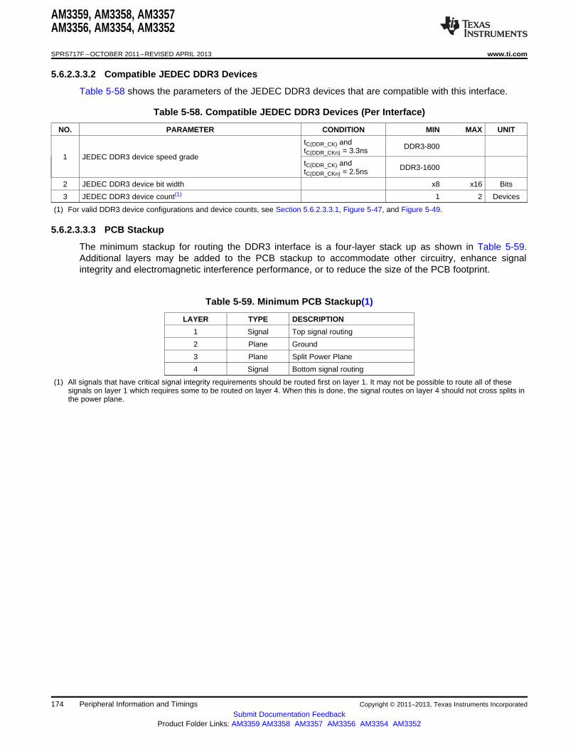
AM3359, AM3358, AM3357AM3356, AM3354, AM3352
SPRS717F –OCTOBER 2011–REVISED APRIL 2013 www.ti.com
5.6.2.3.3.2 Compatible JEDEC DDR3 Devices
Table 5-58 shows the parameters of the JEDEC DDR3 devices that are compatible with this interface.
Table 5-58. Compatible JEDEC DDR3 Devices (Per Interface)
NO. PARAMETER CONDITION MIN MAX UNIT
tC(DDR_CK) and DDR3-800tC(DDR_CKn) = 3.3ns1 JEDEC DDR3 device speed grade
tC(DDR_CK) and DDR3-1600tC(DDR_CKn) = 2.5ns
2 JEDEC DDR3 device bit width x8 x16 Bits
3 JEDEC DDR3 device count(1) 1 2 Devices
(1) For valid DDR3 device configurations and device counts, see Section 5.6.2.3.3.1, Figure 5-47, and Figure 5-49.
5.6.2.3.3.3 PCB Stackup
The minimum stackup for routing the DDR3 interface is a four-layer stack up as shown in Table 5-59.Additional layers may be added to the PCB stackup to accommodate other circuitry, enhance signalintegrity and electromagnetic interference performance, or to reduce the size of the PCB footprint.
Table 5-59. Minimum PCB Stackup(1)
LAYER TYPE DESCRIPTION
1 Signal Top signal routing
2 Plane Ground
3 Plane Split Power Plane
4 Signal Bottom signal routing
(1) All signals that have critical signal integrity requirements should be routed first on layer 1. It may not be possible to route all of thesesignals on layer 1 which requires some to be routed on layer 4. When this is done, the signal routes on layer 4 should not cross splits inthe power plane.
174 Peripheral Information and Timings Copyright © 2011–2013, Texas Instruments Incorporated
Submit Documentation FeedbackProduct Folder Links: AM3359 AM3358 AM3357 AM3356 AM3354 AM3352
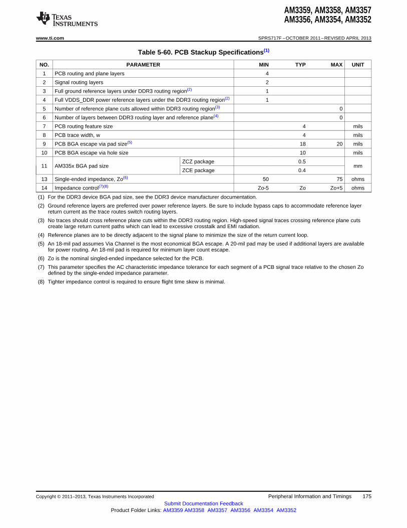
AM3359, AM3358, AM3357AM3356, AM3354, AM3352
www.ti.com SPRS717F –OCTOBER 2011–REVISED APRIL 2013
Table 5-60. PCB Stackup Specifications(1)
NO. PARAMETER MIN TYP MAX UNIT
1 PCB routing and plane layers 4
2 Signal routing layers 2
3 Full ground reference layers under DDR3 routing region(2) 1
4 Full VDDS_DDR power reference layers under the DDR3 routing region(2) 1
5 Number of reference plane cuts allowed within DDR3 routing region(3) 0
6 Number of layers between DDR3 routing layer and reference plane(4) 0
7 PCB routing feature size 4 mils
8 PCB trace width, w 4 mils
9 PCB BGA escape via pad size(5) 18 20 mils
10 PCB BGA escape via hole size 10 mils
ZCZ package 0.511 AM335x BGA pad size mm
ZCE package 0.4
13 Single-ended impedance, Zo(6) 50 75 ohms
14 Impedance control(7)(8) Zo-5 Zo Zo+5 ohms
(1) For the DDR3 device BGA pad size, see the DDR3 device manufacturer documentation.
(2) Ground reference layers are preferred over power reference layers. Be sure to include bypass caps to accommodate reference layerreturn current as the trace routes switch routing layers.
(3) No traces should cross reference plane cuts within the DDR3 routing region. High-speed signal traces crossing reference plane cutscreate large return current paths which can lead to excessive crosstalk and EMI radiation.
(4) Reference planes are to be directly adjacent to the signal plane to minimize the size of the return current loop.
(5) An 18-mil pad assumes Via Channel is the most economical BGA escape. A 20-mil pad may be used if additional layers are availablefor power routing. An 18-mil pad is required for minimum layer count escape.
(6) Zo is the nominal singled-ended impedance selected for the PCB.
(7) This parameter specifies the AC characteristic impedance tolerance for each segment of a PCB signal trace relative to the chosen Zodefined by the single-ended impedance parameter.
(8) Tighter impedance control is required to ensure flight time skew is minimal.
Copyright © 2011–2013, Texas Instruments Incorporated Peripheral Information and Timings 175Submit Documentation Feedback
Product Folder Links: AM3359 AM3358 AM3357 AM3356 AM3354 AM3352

DDR3
Interface
Y
X1
X2
AM3359, AM3358, AM3357AM3356, AM3354, AM3352
SPRS717F –OCTOBER 2011–REVISED APRIL 2013 www.ti.com
5.6.2.3.3.4 Placement
Figure 5-50 shows the required placement for the AM335x device as well as the DDR3 devices. Thedimensions for this figure are defined in Table 5-61. The placement does not restrict the side of the PCBon which the devices are mounted. The ultimate purpose of the placement is to limit the maximum tracelengths and allow for proper routing space.
Figure 5-50. Placement Specifications
Table 5-61. Placement Specifications(1)
NO. PARAMETER MIN MAX UNIT
1 X1(2)(3)(4) 1000 mils
2 X2(2)(3) 600 mils
3 Y Offset(2)(3)(4) 1500 mils
4 Clearance from non-DDR3 signal to DDR3 keepout region(5)(6) 4 w
(1) DDR3 keepout region to encompass entire DDR3 routing area.
(2) For dimension definitions, see Figure 5-50.
(3) Measurements from center of AM335x device to center of DDR3 device.
(4) Minimizing X1 and Y improves timing margins.
(5) w is defined as the signal trace width.
(6) Non-DDR3 signals allowed within DDR3 keepout region provided they are separated from DDR3 routing layers by a ground plane.
176 Peripheral Information and Timings Copyright © 2011–2013, Texas Instruments Incorporated
Submit Documentation FeedbackProduct Folder Links: AM3359 AM3358 AM3357 AM3356 AM3354 AM3352

DDR3 Keepout Region
DDR3 Interface
Encompasses EntireDDR3 Routing Area
AM3359, AM3358, AM3357AM3356, AM3354, AM3352
www.ti.com SPRS717F –OCTOBER 2011–REVISED APRIL 2013
5.6.2.3.3.5 DDR3 Keepout Region
The region of the PCB used for DDR3 circuitry must be isolated from other signals. The DDR3 keepoutregion is defined for this purpose and is shown in Figure 5-51. This region should encompass all DDR3circuitry and the region size varies with component placement and DDR3 routing. Additional clearancesrequired for the keepout region are shown in Table 5-61. Non-DDR3 signals should not be routed on thesame signal layer as DDR3 signals within the DDR3 keepout region. Non-DDR3 signals may be routed inthe region provided they are routed on layers separated from DDR3 signal layers by a ground layer. Nobreaks should be allowed in the reference ground or VDDS_DDR power plane in this region. In addition,the VDDS_DDR power plane should cover the entire keepout region.
Figure 5-51. DDR3 Keepout Region
5.6.2.3.3.6 Bulk Bypass Capacitors
Bulk bypass capacitors are required for moderate speed bypassing of the DDR3 and other circuitry.Table 5-62 contains the minimum numbers and capacitance required for the bulk bypass capacitors. Notethat this table only covers the bypass needs of the AM335x DDR3 interface and DDR3 devices. Additionalbulk bypass capacitance may be needed for other circuitry.
Table 5-62. Bulk Bypass Capacitors(1)
NO. PARAMETER MIN MAX UNIT
1 AM335x VDDS_DDR bulk bypass capacitor count 2 Devices
2 AM335x VDDS_DDR bulk bypass total capacitance 20 μF
3 DDR3#1 bulk bypass capacitor count 2 Devices
4 DDR3#1 bulk bypass total capacitance 20 μF
5 DDR3#2 bulk bypass capacitor count(2) 2 Devices
6 DDR3#2 bulk bypass total capacitance(2) 20 μF
(1) These devices should be placed near the devices they are bypassing, but preference should be given to the placement of the high-speed (HS) bypass capacitors and DDR3 signal routing.
(2) Only used when two DDR3 devices are used.
Copyright © 2011–2013, Texas Instruments Incorporated Peripheral Information and Timings 177Submit Documentation Feedback
Product Folder Links: AM3359 AM3358 AM3357 AM3356 AM3354 AM3352

AM3359, AM3358, AM3357AM3356, AM3354, AM3352
SPRS717F –OCTOBER 2011–REVISED APRIL 2013 www.ti.com
5.6.2.3.3.7 High-Speed Bypass Capacitors
High-speed (HS) bypass capacitors are critcal for proper DDR3 interface operation. It is particularlyimportant to minimize the parasitic series inductance of the HS bypass capacitors, AM335x device DDR3power, and AM335x device DDR3 ground connections. Table 5-63 contains the specification for the HSbypass capacitors as well as for the power connections on the PCB. Generally speaking, it is good to:
1. Fit as many HS bypass capacitors as possible.
2. Minimize the distance from the bypass cap to the power terminals being bypassed.
3. Use the smallest physical sized capacitors possible with the highest capacitance readily available.
4. Connect the bypass capacitor pads to their vias using the widest traces possible and using the largesthole size via possible.
5. Minimize via sharing. Note the limites on via sharing shown in Table 5-63.
Table 5-63. High-Speed Bypass Capacitors
NO. PARAMETER MIN TYP MAX UNIT
1 HS bypass capacitor package size(1) 0201 0402 10 mils
2 Distance, HS bypass capacitor to AM335x VDDS_DDR and VSS terminal 400 milsbeing bypassed(2)(3)(4)
3 AM335x VDDS_DDR HS bypass capacitor count 20 Devices
4 AM335x VDDS_DDR HS bypass capacitor total capacitance 1 μF
5 Trace length from AM335x VDDS_DDR and VSS terminal to connection 35 70 milsvia(2)
6 Distance, HS bypass capacitor to DDR3 device being bypassed(5) 150 mils
7 DDR3 device HS bypass capacitor count(6) 12 Devices
8 DDR3 device HS bypass capacitor total capacitance(6) 0.85 μF
9 Number of connection vias for each HS bypass capacitor(7)(8) 2 Vias
10 Trace length from bypass capacitor connect to connection via(2)(8) 35 100 mils
11 Number of connection vias for each DDR3 device power and ground 1 Viasterminal(9)
12 Trace length from DDR3 device power and ground terminal to connection 35 60 milsvia(2)(7)
(1) LxW, 10-mil units; for example, a 0402 is a 40x20-mil surface-mount capacitor.
(2) Closer and shorter is better.
(3) Measured from the nearest AM335x VDDS_DDR and ground terminal to the center of the capacitor package.
(4) Three of these capacitors should be located underneath the AM335x device, between the cluster of VDDS_DDR and ground terminals,between the DDR3 interfaces on the package.
(5) Measured from the DDR3 device power and ground terminal to the center of the capacitor package.
(6) Per DDR3 device.
(7) An additional HS bypass capacitor can share the connection vias only if it is mounted on the opposite side of the board. No sharing ofvias is permitted on the same side of the board.
(8) An HS bypass capacitor may share a via with a DDR3 device mounted on the same side of the PCB. A wide trace should be used forthe connection and the length from the capacitor pad to the DDR3 device pad should be less than 150 mils.
(9) Up to a total of two pairs of DDR3 power and ground terminals may share a via.
5.6.2.3.3.7.1 Return Current Bypass Capacitors
Use additional bypass capacitors if the return current reference plane changes due to DDR3 signalshopping from one signal layer to another. The bypass capacitor here provides a path for the return currentto hop planes along with the signal. As many of these return current bypass capacitors should be used aspossible. Since these are returns for signal current, the signal via size may be used for these capacitors.
178 Peripheral Information and Timings Copyright © 2011–2013, Texas Instruments Incorporated
Submit Documentation FeedbackProduct Folder Links: AM3359 AM3358 AM3357 AM3356 AM3354 AM3352
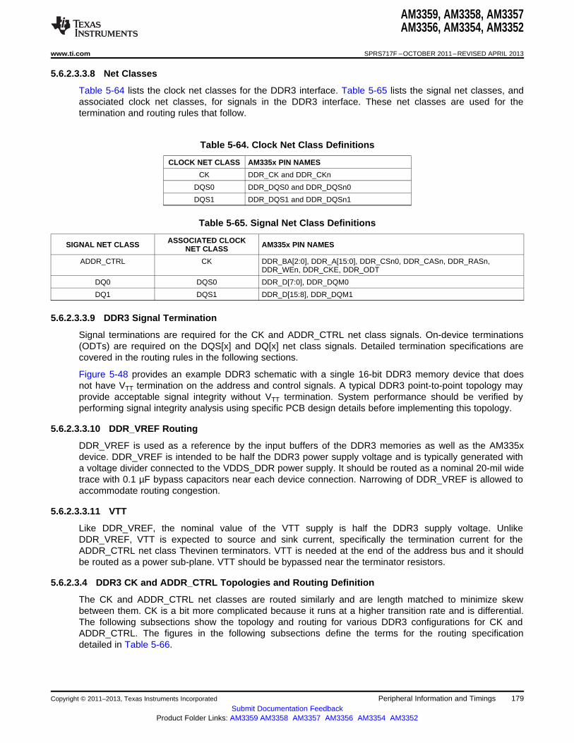
AM3359, AM3358, AM3357AM3356, AM3354, AM3352
www.ti.com SPRS717F –OCTOBER 2011–REVISED APRIL 2013
5.6.2.3.3.8 Net Classes
Table 5-64 lists the clock net classes for the DDR3 interface. Table 5-65 lists the signal net classes, andassociated clock net classes, for signals in the DDR3 interface. These net classes are used for thetermination and routing rules that follow.
Table 5-64. Clock Net Class Definitions
CLOCK NET CLASS AM335x PIN NAMES
CK DDR_CK and DDR_CKn
DQS0 DDR_DQS0 and DDR_DQSn0
DQS1 DDR_DQS1 and DDR_DQSn1
Table 5-65. Signal Net Class Definitions
ASSOCIATED CLOCKSIGNAL NET CLASS AM335x PIN NAMESNET CLASS
ADDR_CTRL CK DDR_BA[2:0], DDR_A[15:0], DDR_CSn0, DDR_CASn, DDR_RASn,DDR_WEn, DDR_CKE, DDR_ODT
DQ0 DQS0 DDR_D[7:0], DDR_DQM0
DQ1 DQS1 DDR_D[15:8], DDR_DQM1
5.6.2.3.3.9 DDR3 Signal Termination
Signal terminations are required for the CK and ADDR_CTRL net class signals. On-device terminations(ODTs) are required on the DQS[x] and DQ[x] net class signals. Detailed termination specifications arecovered in the routing rules in the following sections.
Figure 5-48 provides an example DDR3 schematic with a single 16-bit DDR3 memory device that doesnot have VTT termination on the address and control signals. A typical DDR3 point-to-point topology mayprovide acceptable signal integrity without VTT termination. System performance should be verified byperforming signal integrity analysis using specific PCB design details before implementing this topology.
5.6.2.3.3.10 DDR_VREF Routing
DDR_VREF is used as a reference by the input buffers of the DDR3 memories as well as the AM335xdevice. DDR_VREF is intended to be half the DDR3 power supply voltage and is typically generated witha voltage divider connected to the VDDS_DDR power supply. It should be routed as a nominal 20-mil widetrace with 0.1 µF bypass capacitors near each device connection. Narrowing of DDR_VREF is allowed toaccommodate routing congestion.
5.6.2.3.3.11 VTT
Like DDR_VREF, the nominal value of the VTT supply is half the DDR3 supply voltage. UnlikeDDR_VREF, VTT is expected to source and sink current, specifically the termination current for theADDR_CTRL net class Thevinen terminators. VTT is needed at the end of the address bus and it shouldbe routed as a power sub-plane. VTT should be bypassed near the terminator resistors.
5.6.2.3.4 DDR3 CK and ADDR_CTRL Topologies and Routing Definition
The CK and ADDR_CTRL net classes are routed similarly and are length matched to minimize skewbetween them. CK is a bit more complicated because it runs at a higher transition rate and is differential.The following subsections show the topology and routing for various DDR3 configurations for CK andADDR_CTRL. The figures in the following subsections define the terms for the routing specificationdetailed in Table 5-66.
Copyright © 2011–2013, Texas Instruments Incorporated Peripheral Information and Timings 179Submit Documentation Feedback
Product Folder Links: AM3359 AM3358 AM3357 AM3356 AM3354 AM3352
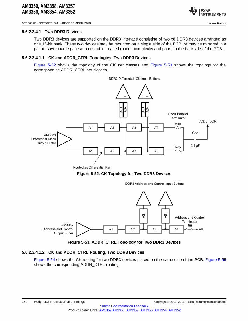
A1 A2
AM335x
Address and Control
Output Buffer
DDR3 Address and Control Input Buffers
A3 AT Vtt
Address and Control
Terminator
Rtt
AS
AS
AS
-
AS
+
A1 A2
AM335x
Differential Clock
Output Buffer
DDR3 Differential CK Input Buffers
Routed as Differential Pair
A3 AT
Rcp
Clock Parallel
Terminator
A1 A2 A3 AT
AS
-
AS
+
Rcp
Cac
VDDS_DDR
0.1 µF
+
–
+ – + –
AM3359, AM3358, AM3357AM3356, AM3354, AM3352
SPRS717F –OCTOBER 2011–REVISED APRIL 2013 www.ti.com
5.6.2.3.4.1 Two DDR3 Devices
Two DDR3 devices are supported on the DDR3 interface consisting of two x8 DDR3 devices arranged asone 16-bit bank. These two devices may be mounted on a single side of the PCB, or may be mirrored in apair to save board space at a cost of increased routing complexity and parts on the backside of the PCB.
5.6.2.3.4.1.1 CK and ADDR_CTRL Topologies, Two DDR3 Devices
Figure 5-52 shows the topology of the CK net classes and Figure 5-53 shows the topology for thecorresponding ADDR_CTRL net classes.
Figure 5-52. CK Topology for Two DDR3 Devices
Figure 5-53. ADDR_CTRL Topology for Two DDR3 Devices
5.6.2.3.4.1.2 CK and ADDR_CTRL Routing, Two DDR3 Devices
Figure 5-54 shows the CK routing for two DDR3 devices placed on the same side of the PCB. Figure 5-55shows the corresponding ADDR_CTRL routing.
180 Peripheral Information and Timings Copyright © 2011–2013, Texas Instruments Incorporated
Submit Documentation FeedbackProduct Folder Links: AM3359 AM3358 AM3357 AM3356 AM3354 AM3352
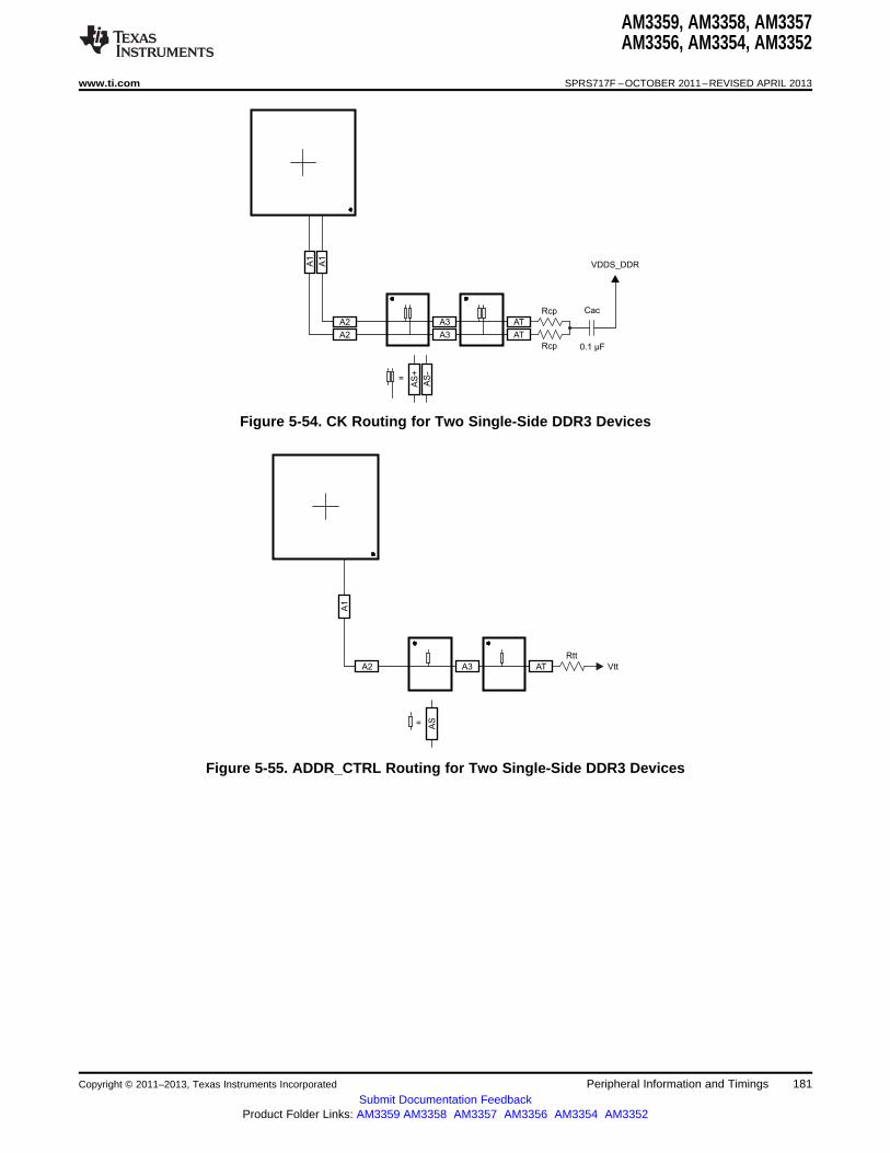
AS=
Rtt
A1
A2 A3 AT Vtt
AS
+
AS
-
=
Rcp
Rcp
Cac
VDDS_DDR
0.1 µF
A1
A2 A3 AT
A2 A3 AT
A1
AM3359, AM3358, AM3357AM3356, AM3354, AM3352
www.ti.com SPRS717F –OCTOBER 2011–REVISED APRIL 2013
Figure 5-54. CK Routing for Two Single-Side DDR3 Devices
Figure 5-55. ADDR_CTRL Routing for Two Single-Side DDR3 Devices
Copyright © 2011–2013, Texas Instruments Incorporated Peripheral Information and Timings 181Submit Documentation Feedback
Product Folder Links: AM3359 AM3358 AM3357 AM3356 AM3354 AM3352
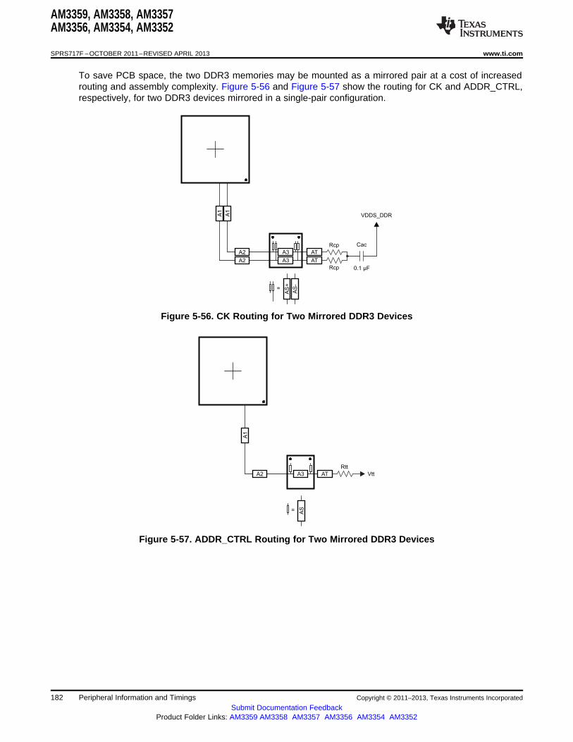
AS=
Rtt
A1
A2 A3 AT Vtt
AS
+
AS
-=
Rcp
Rcp
Cac
VDDS_DDR
0.1 µF
A1
A2 A3 AT
A2 A3 AT
A1
AM3359, AM3358, AM3357AM3356, AM3354, AM3352
SPRS717F –OCTOBER 2011–REVISED APRIL 2013 www.ti.com
To save PCB space, the two DDR3 memories may be mounted as a mirrored pair at a cost of increasedrouting and assembly complexity. Figure 5-56 and Figure 5-57 show the routing for CK and ADDR_CTRL,respectively, for two DDR3 devices mirrored in a single-pair configuration.
Figure 5-56. CK Routing for Two Mirrored DDR3 Devices
Figure 5-57. ADDR_CTRL Routing for Two Mirrored DDR3 Devices
182 Peripheral Information and Timings Copyright © 2011–2013, Texas Instruments Incorporated
Submit Documentation FeedbackProduct Folder Links: AM3359 AM3358 AM3357 AM3356 AM3354 AM3352

A1 A2
AM335x
Address and Control
Output Buffer
DDR3 Address and Control Input Buffers
AT Vtt
Address and Control
Terminator
Rtt
AS
A1 A2
AM335x
Differential Clock
Output Buffer
DDR3 Differential CK Input Buffer
Routed as Differential Pair
AT
Rcp
Clock Parallel
Terminator
A1 A2 AT
AS
-
AS
+
Rcp
Cac
VDDS_DDR
0.1 µF
+
–
+ –
AM3359, AM3358, AM3357AM3356, AM3354, AM3352
www.ti.com SPRS717F –OCTOBER 2011–REVISED APRIL 2013
5.6.2.3.4.2 One DDR3 Device
A single DDR3 device is supported on the DDR3 interface consisting of one x16 DDR3 device arrangedas one 16-bit bank.
5.6.2.3.4.2.1 CK and ADDR_CTRL Topologies, One DDR3 Device
Figure 5-58 shows the topology of the CK net classes and Figure 5-59 shows the topology for thecorresponding ADDR_CTRL net classes.
Figure 5-58. CK Topology for One DDR3 Device
Figure 5-59. ADDR_CTRL Topology for One DDR3 Device
Copyright © 2011–2013, Texas Instruments Incorporated Peripheral Information and Timings 183Submit Documentation Feedback
Product Folder Links: AM3359 AM3358 AM3357 AM3356 AM3354 AM3352

AS=
Rtt
A1
A2 AT Vtt
AS
+
AS
-=
Rcp
Rcp
Cac
VDDS_DDR
0.1 µF
A1
A2 AT
A2 AT
A1
AM3359, AM3358, AM3357AM3356, AM3354, AM3352
SPRS717F –OCTOBER 2011–REVISED APRIL 2013 www.ti.com
5.6.2.3.4.2.2 CK and ADDR_CTRL Routing, One DDR3 Device
Figure 5-60 shows the CK routing for one DDR3 device. Figure 5-61 shows the correspondingADDR_CTRL routing.
Figure 5-60. CK Routing for One DDR3 Device
Figure 5-61. ADDR_CTRL Routing for One DDR3 Device
5.6.2.3.5 Data Topologies and Routing Definition
No matter the number of DDR3 devices used, the data line topology is always point to point, so itsdefinition is simple.
5.6.2.3.5.1 DQS[x] and DQ[x] Topologies, Any Number of Allowed DDR3 Devices
DQS[x] lines are point-to-point differential, and DQ[x] lines are point-to-point singled ended. Figure 5-62and Figure 5-63 show these topologies.
184 Peripheral Information and Timings Copyright © 2011–2013, Texas Instruments Incorporated
Submit Documentation FeedbackProduct Folder Links: AM3359 AM3358 AM3357 AM3356 AM3354 AM3352
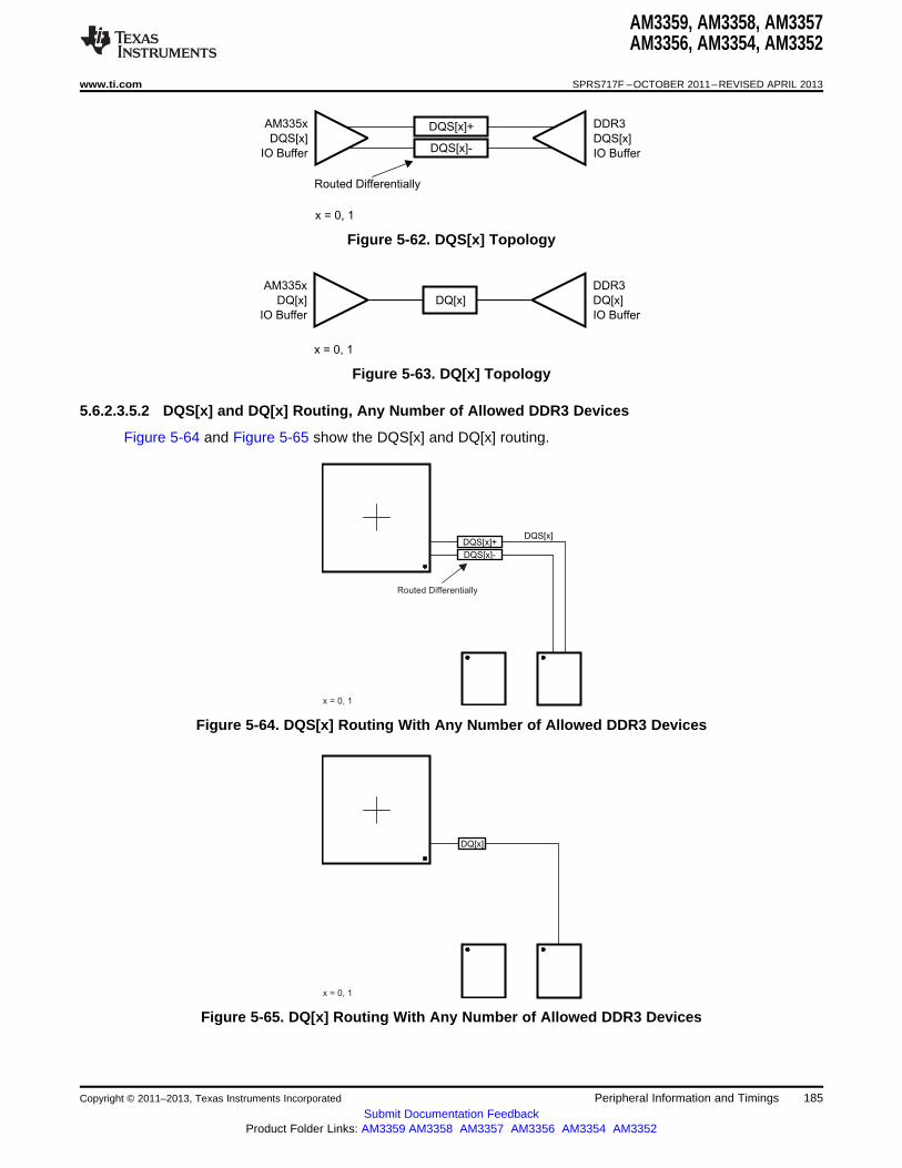
DQ[x]
x = 0, 1
DQS[x]+
DQS[x]-
x = 0, 1
Routed Differentially
DQS[x]
DQ[x]
AM335x
DQ[x]
IO Buffer
DDR3
DQ[x]
IO Buffer
x = 0, 1
AM335x
DQS[x]
IO Buffer
DDR3
DQS[x]
IO Buffer
Routed Differentially
x = 0, 1
DQS[x]-
DQS[x]+
AM3359, AM3358, AM3357AM3356, AM3354, AM3352
www.ti.com SPRS717F –OCTOBER 2011–REVISED APRIL 2013
Figure 5-62. DQS[x] Topology
Figure 5-63. DQ[x] Topology
5.6.2.3.5.2 DQS[x] and DQ[x] Routing, Any Number of Allowed DDR3 Devices
Figure 5-64 and Figure 5-65 show the DQS[x] and DQ[x] routing.
Figure 5-64. DQS[x] Routing With Any Number of Allowed DDR3 Devices
Figure 5-65. DQ[x] Routing With Any Number of Allowed DDR3 Devices
Copyright © 2011–2013, Texas Instruments Incorporated Peripheral Information and Timings 185Submit Documentation Feedback
Product Folder Links: AM3359 AM3358 AM3357 AM3356 AM3354 AM3352
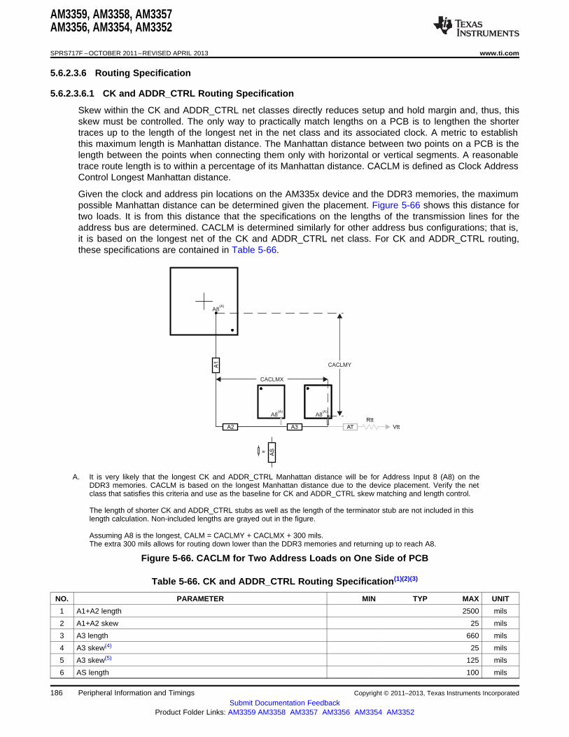
AS=
Rtt
A1
A2 A3 AT Vtt
A8(A)
A8(A)
A8(A)
CACLMX
CACLMY
AM3359, AM3358, AM3357AM3356, AM3354, AM3352
SPRS717F –OCTOBER 2011–REVISED APRIL 2013 www.ti.com
5.6.2.3.6 Routing Specification
5.6.2.3.6.1 CK and ADDR_CTRL Routing Specification
Skew within the CK and ADDR_CTRL net classes directly reduces setup and hold margin and, thus, thisskew must be controlled. The only way to practically match lengths on a PCB is to lengthen the shortertraces up to the length of the longest net in the net class and its associated clock. A metric to establishthis maximum length is Manhattan distance. The Manhattan distance between two points on a PCB is thelength between the points when connecting them only with horizontal or vertical segments. A reasonabletrace route length is to within a percentage of its Manhattan distance. CACLM is defined as Clock AddressControl Longest Manhattan distance.
Given the clock and address pin locations on the AM335x device and the DDR3 memories, the maximumpossible Manhattan distance can be determined given the placement. Figure 5-66 shows this distance fortwo loads. It is from this distance that the specifications on the lengths of the transmission lines for theaddress bus are determined. CACLM is determined similarly for other address bus configurations; that is,it is based on the longest net of the CK and ADDR_CTRL net class. For CK and ADDR_CTRL routing,these specifications are contained in Table 5-66.
A. It is very likely that the longest CK and ADDR_CTRL Manhattan distance will be for Address Input 8 (A8) on theDDR3 memories. CACLM is based on the longest Manhattan distance due to the device placement. Verify the netclass that satisfies this criteria and use as the baseline for CK and ADDR_CTRL skew matching and length control.
The length of shorter CK and ADDR_CTRL stubs as well as the length of the terminator stub are not included in thislength calculation. Non-included lengths are grayed out in the figure.
Assuming A8 is the longest, CALM = CACLMY + CACLMX + 300 mils.The extra 300 mils allows for routing down lower than the DDR3 memories and returning up to reach A8.
Figure 5-66. CACLM for Two Address Loads on One Side of PCB
Table 5-66. CK and ADDR_CTRL Routing Specification(1)(2)(3)
NO. PARAMETER MIN TYP MAX UNIT
1 A1+A2 length 2500 mils
2 A1+A2 skew 25 mils
3 A3 length 660 mils
4 A3 skew(4) 25 mils
5 A3 skew(5) 125 mils
6 AS length 100 mils
186 Peripheral Information and Timings Copyright © 2011–2013, Texas Instruments Incorporated
Submit Documentation FeedbackProduct Folder Links: AM3359 AM3358 AM3357 AM3356 AM3354 AM3352

AM3359, AM3358, AM3357AM3356, AM3354, AM3352
www.ti.com SPRS717F –OCTOBER 2011–REVISED APRIL 2013
Table 5-66. CK and ADDR_CTRL Routing Specification(1)(2)(3) (continued)
NO. PARAMETER MIN TYP MAX UNIT
7 AS skew 25 mils
8 AS+ and AS- length 70 mils
9 AS+ and AS- skew 5 mils
10 AT length(6) 500 mils
11 AT skew(7) 100 mils
12 AT skew(8) 5 mils
13 CK and ADDR_CTRL nominal trace length(9) CACLM-50 CACLM CACLM+50 mils
14 Center-to-center CK to other DDR3 trace spacing(10) 4w
15 Center-to-center ADDR_CTRL to other DDR3 trace spacing(10)(11) 4w
16 Center-to-center ADDR_CTRL to other ADDR_CTRL trace spacing(10) 3w
17 CK center-to-center spacing(12)
18 CK spacing to other net(10) 4w
19 Rcp(13) Zo-1 Zo Zo+1 ohms
20 Rtt(13)(14) Zo-5 Zo Zo+5 ohms
(1) CK represents the clock net class, and ADDR_CTRL represents the address and control signal net class.
(2) The use of vias should be minimized.
(3) Additional bypass capacitors are required when using the VDDS_DDR plane as the reference plane to allow the return current to jumpbetween the VDDS_DDR plane and the ground plane when the net class switches layers at a via.
(4) Mirrored configuration (one DDR3 device on top of the board and one DDR3 device on the bottom).
(5) Non-mirrored configuration (all DDR3 memories on same side of PCB).
(6) While this length can be increased for convenience, its length should be minimized.
(7) ADDR_CTRL net class only (not CK net class). Minimizing this skew is recommended, but not required.
(8) CK net class only.
(9) CACLM is the longest Manhattan distance of the CK and ADDR_CTRL net classes + 300 mils. For definition, see Section 5.6.2.3.6.1and Figure 5-66.
(10) Center-to-center spacing is allowed to fall to minimum (w) for up to 1250 mils of routed length.
(11) Signals from one DQ net class should be considered other DDR3 traces to another DQ net class.
(12) CK spacing set to ensure proper differential impedance. Differential impedance should be Zo x 2, where Zo is the single-endedimpedance defined in Table 5-60.
(13) Source termination (series resistor at driver) is specifically not allowed.
(14) Termination values should be uniform across the net class.
5.6.2.3.6.2 DQS[x] and DQ[x] Routing Specification
Skew within the DQS[x] and DQ[x] net classes directly reduces setup and hold margin and, thus, this skewmust be controlled. The only way to practically match lengths on a PCB is to lengthen the shorter tracesup to the length of the longest net in the net class and its associated clock. DQLMn is defined as DQLongest Manhattan distance n, where n is the byte number. For a 16-bit interface, there are two DQLMs,DQLM0-DQLM1.
NOTEIt is not required, nor is it recommended, to match the lengths across all bytes. Lengthmatching is only required within each byte.
Given the DQS[x] and DQ[x] pin locations on the AM335x device and the DDR3 memories, the maximumpossible Manhattan distance can be determined given the placement. Figure 5-67 shows this distance fora two-load case. It is from this distance that the specifications on the lengths of the transmission lines forthe data bus are determined. For DQS[x] and DQ[x] routing, these specifications are contained in Table 5-67.
Copyright © 2011–2013, Texas Instruments Incorporated Peripheral Information and Timings 187Submit Documentation Feedback
Product Folder Links: AM3359 AM3358 AM3357 AM3356 AM3354 AM3352

DQLMY0
1 0
DQLMX1
DQ1
DQ0
DQLMX0
DQ[8:15], DM1, DQS1
DQ[0:7], DM0, DQS0
DQLMY1
DQ0 - DQ1 represent data bytes 0 - 1.
AM3359, AM3358, AM3357AM3356, AM3354, AM3352
SPRS717F –OCTOBER 2011–REVISED APRIL 2013 www.ti.com
There are two DQLMs, one for each byte (16-bit interface). Each DQLM is the longest Manhattan distance of the byte;therefore:DQLM0 = DQLMX0 + DQLMY0DQLM1 = DQLMX1 + DQLMY1
Figure 5-67. DQLM for Any Number of Allowed DDR3 Devices
Table 5-67. DQS[x] and DQ[x] Routing Specification(1)(2)
NO. PARAMETER MIN TYP MAX UNIT
1 DQ0 nominal length(3)(4) DQLM0 mils
2 DQ1 nominal length(3)(5) DQLM1 mils
3 DQ[x] skew(6) 25 mils
4 DQS[x] skew 5 mils
5 DQS[x]-to-DQ[x] skew(6)(7) 25 mils
6 Center-to-center DQ[x] to other DDR3 trace spacing(8)(9) 4w
7 Center-to-center DQ[x] to other DQ[x] trace spacing(8)(10) 3w
8 DQS[x] center-to-center spacing(11)
9 DQS[x] center-to-center spacing to other net(8) 4w
(1) DQS[x] represents the DQS0 and DQS1 clock net classes, and DQ[x] represents the DQ0 and DQ1 signal net classes.
(2) External termination disallowed. Data termination should use built-in ODT functionality.
(3) DQLMn is the longest Manhattan distance of a byte. For definition, see Section 5.6.2.3.6.2 and Figure 5-67.
(4) DQLM0 is the longest Manhattan length for the DQ0 net class.
(5) DQLM1 is the longest Manhattan length for the DQ1 net class.
(6) Length matching is only done within a byte. Length matching across bytes is not required.
(7) Each DQS clock net class is length matched to its associated DQ signal net class.
(8) Center-to-center spacing is allowed to fall to minimum for up to 1250 mils of routed length.
(9) Other DDR3 trace spacing means signals that are not part of the same DQ[x] signal net class.
(10) This applies to spacing within same DQ[x] signal net class.
(11) DQS[x] pair spacing is set to ensure proper differential impedance. Differential impedance should be Zo x 2, where Zo is the single-ended impedance defined in Table 5-60.
188 Peripheral Information and Timings Copyright © 2011–2013, Texas Instruments Incorporated
Submit Documentation FeedbackProduct Folder Links: AM3359 AM3358 AM3357 AM3356 AM3354 AM3352
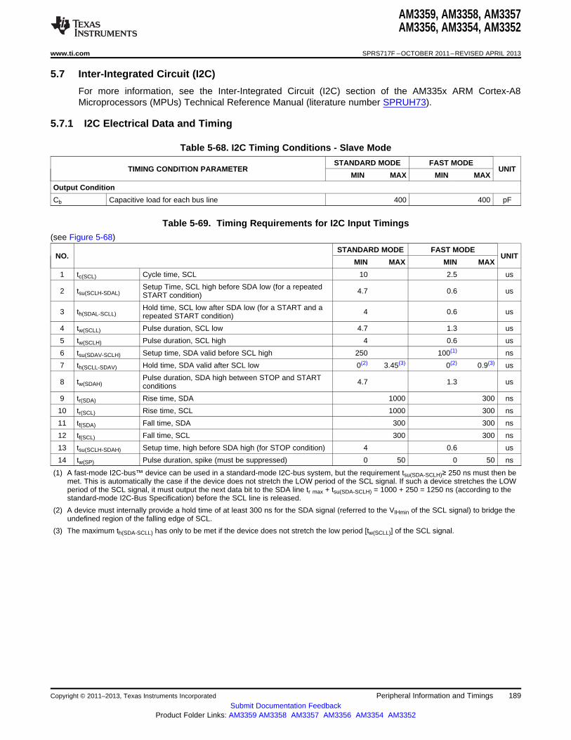
AM3359, AM3358, AM3357AM3356, AM3354, AM3352
www.ti.com SPRS717F –OCTOBER 2011–REVISED APRIL 2013
5.7 Inter-Integrated Circuit (I2C)
For more information, see the Inter-Integrated Circuit (I2C) section of the AM335x ARM Cortex-A8Microprocessors (MPUs) Technical Reference Manual (literature number SPRUH73).
5.7.1 I2C Electrical Data and Timing
Table 5-68. I2C Timing Conditions - Slave Mode
STANDARD MODE FAST MODETIMING CONDITION PARAMETER UNIT
MIN MAX MIN MAX
Output Condition
Cb Capacitive load for each bus line 400 400 pF
Table 5-69. Timing Requirements for I2C Input Timings(see Figure 5-68)
STANDARD MODE FAST MODENO. UNIT
MIN MAX MIN MAX
1 tc(SCL) Cycle time, SCL 10 2.5 us
Setup Time, SCL high before SDA low (for a repeated2 tsu(SCLH-SDAL) 4.7 0.6 usSTART condition)
Hold time, SCL low after SDA low (for a START and a3 th(SDAL-SCLL) 4 0.6 usrepeated START condition)
4 tw(SCLL) Pulse duration, SCL low 4.7 1.3 us
5 tw(SCLH) Pulse duration, SCL high 4 0.6 us
6 tsu(SDAV-SCLH) Setup time, SDA valid before SCL high 250 100(1) ns
7 th(SCLL-SDAV) Hold time, SDA valid after SCL low 0(2) 3.45(3) 0(2) 0.9(3) us
Pulse duration, SDA high between STOP and START8 tw(SDAH) 4.7 1.3 usconditions
9 tr(SDA) Rise time, SDA 1000 300 ns
10 tr(SCL) Rise time, SCL 1000 300 ns
11 tf(SDA) Fall time, SDA 300 300 ns
12 tf(SCL) Fall time, SCL 300 300 ns
13 tsu(SCLH-SDAH) Setup time, high before SDA high (for STOP condition) 4 0.6 us
14 tw(SP) Pulse duration, spike (must be suppressed) 0 50 0 50 ns
(1) A fast-mode I2C-bus™ device can be used in a standard-mode I2C-bus system, but the requirement tsu(SDA-SCLH)≥ 250 ns must then bemet. This is automatically the case if the device does not stretch the LOW period of the SCL signal. If such a device stretches the LOWperiod of the SCL signal, it must output the next data bit to the SDA line tr max + tsu(SDA-SCLH) = 1000 + 250 = 1250 ns (according to thestandard-mode I2C-Bus Specification) before the SCL line is released.
(2) A device must internally provide a hold time of at least 300 ns for the SDA signal (referred to the VIHmin of the SCL signal) to bridge theundefined region of the falling edge of SCL.
(3) The maximum th(SDA-SCLL) has only to be met if the device does not stretch the low period [tw(SCLL)] of the SCL signal.
Copyright © 2011–2013, Texas Instruments Incorporated Peripheral Information and Timings 189Submit Documentation Feedback
Product Folder Links: AM3359 AM3358 AM3357 AM3356 AM3354 AM3352
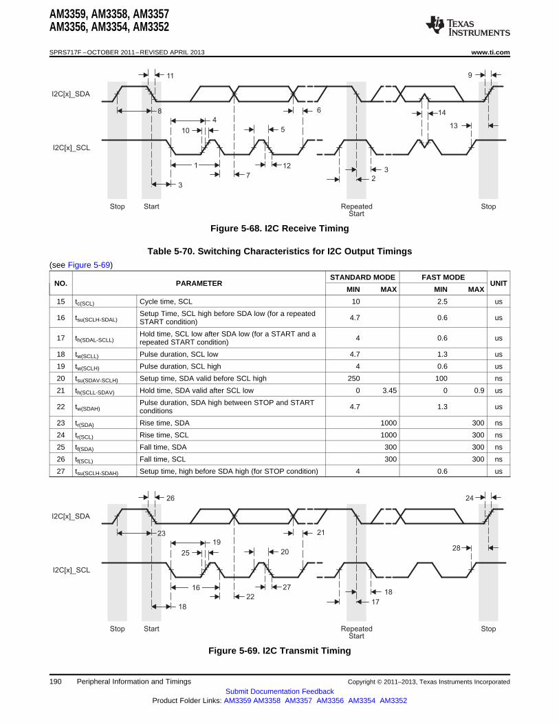
25
23
19
18
22
27
20
21
17
18
28
Stop Start RepeatedStart
Stop
I2C[x]_SDA
I2C[x]_SCL
16
26 24
10
8
4
3
7
12
5
6 14
2
3
13
Stop Start RepeatedStart
Stop
I2C[x]_SDA
I2C[x]_SCL
1
11 9
AM3359, AM3358, AM3357AM3356, AM3354, AM3352
SPRS717F –OCTOBER 2011–REVISED APRIL 2013 www.ti.com
Figure 5-68. I2C Receive Timing
Table 5-70. Switching Characteristics for I2C Output Timings(see Figure 5-69)
STANDARD MODE FAST MODENO. PARAMETER UNIT
MIN MAX MIN MAX
15 tc(SCL) Cycle time, SCL 10 2.5 us
Setup Time, SCL high before SDA low (for a repeated16 tsu(SCLH-SDAL) 4.7 0.6 usSTART condition)
Hold time, SCL low after SDA low (for a START and a17 th(SDAL-SCLL) 4 0.6 usrepeated START condition)
18 tw(SCLL) Pulse duration, SCL low 4.7 1.3 us
19 tw(SCLH) Pulse duration, SCL high 4 0.6 us
20 tsu(SDAV-SCLH) Setup time, SDA valid before SCL high 250 100 ns
21 th(SCLL-SDAV) Hold time, SDA valid after SCL low 0 3.45 0 0.9 us
Pulse duration, SDA high between STOP and START22 tw(SDAH) 4.7 1.3 usconditions
23 tr(SDA) Rise time, SDA 1000 300 ns
24 tr(SCL) Rise time, SCL 1000 300 ns
25 tf(SDA) Fall time, SDA 300 300 ns
26 tf(SCL) Fall time, SCL 300 300 ns
27 tsu(SCLH-SDAH) Setup time, high before SDA high (for STOP condition) 4 0.6 us
Figure 5-69. I2C Transmit Timing
190 Peripheral Information and Timings Copyright © 2011–2013, Texas Instruments Incorporated
Submit Documentation FeedbackProduct Folder Links: AM3359 AM3358 AM3357 AM3356 AM3354 AM3352
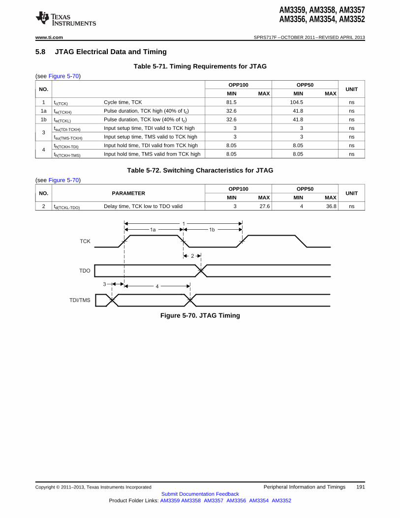
3
TCK
TDO
TDI/TMS
2
4
1
1a 1b
AM3359, AM3358, AM3357AM3356, AM3354, AM3352
www.ti.com SPRS717F –OCTOBER 2011–REVISED APRIL 2013
5.8 JTAG Electrical Data and Timing
Table 5-71. Timing Requirements for JTAG(see Figure 5-70)
OPP100 OPP50NO. UNIT
MIN MAX MIN MAX
1 tc(TCK) Cycle time, TCK 81.5 104.5 ns
1a tw(TCKH) Pulse duration, TCK high (40% of tc) 32.6 41.8 ns
1b tw(TCKL) Pulse duration, TCK low (40% of tc) 32.6 41.8 ns
tsu(TDI-TCKH) Input setup time, TDI valid to TCK high 3 3 ns3
tsu(TMS-TCKH) Input setup time, TMS valid to TCK high 3 3 ns
th(TCKH-TDI) Input hold time, TDI valid from TCK high 8.05 8.05 ns4
th(TCKH-TMS) Input hold time, TMS valid from TCK high 8.05 8.05 ns
Table 5-72. Switching Characteristics for JTAG(see Figure 5-70)
OPP100 OPP50NO. PARAMETER UNIT
MIN MAX MIN MAX
2 td(TCKL-TDO) Delay time, TCK low to TDO valid 3 27.6 4 36.8 ns
Figure 5-70. JTAG Timing
Copyright © 2011–2013, Texas Instruments Incorporated Peripheral Information and Timings 191Submit Documentation Feedback
Product Folder Links: AM3359 AM3358 AM3357 AM3356 AM3354 AM3352
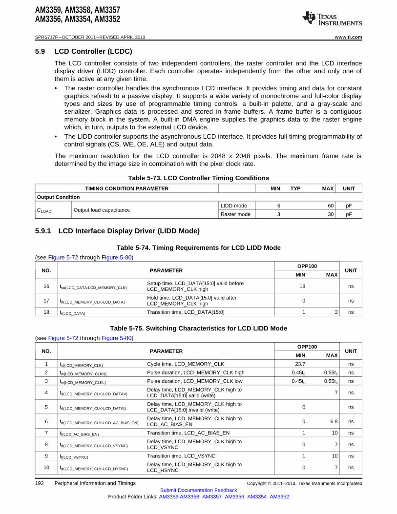
AM3359, AM3358, AM3357AM3356, AM3354, AM3352
SPRS717F –OCTOBER 2011–REVISED APRIL 2013 www.ti.com
5.9 LCD Controller (LCDC)
The LCD controller consists of two independent controllers, the raster controller and the LCD interfacedisplay driver (LIDD) controller. Each controller operates independently from the other and only one ofthem is active at any given time.• The raster controller handles the synchronous LCD interface. It provides timing and data for constant
graphics refresh to a passive display. It supports a wide variety of monochrome and full-color displaytypes and sizes by use of programmable timing controls, a built-in palette, and a gray-scale andserializer. Graphics data is processed and stored in frame buffers. A frame buffer is a contiguousmemory block in the system. A built-in DMA engine supplies the graphics data to the raster enginewhich, in turn, outputs to the external LCD device.
• The LIDD controller supports the asynchronous LCD interface. It provides full-timing programmability ofcontrol signals (CS, WE, OE, ALE) and output data.
The maximum resolution for the LCD controller is 2048 x 2048 pixels. The maximum frame rate isdetermined by the image size in combination with the pixel clock rate.
Table 5-73. LCD Controller Timing Conditions
TIMING CONDITION PARAMETER MIN TYP MAX UNIT
Output Condition
LIDD mode 5 60 pFCLOAD Output load capacitance
Raster mode 3 30 pF
5.9.1 LCD Interface Display Driver (LIDD Mode)
Table 5-74. Timing Requirements for LCD LIDD Mode(see Figure 5-72 through Figure 5-80)
OPP100NO. PARAMETER UNIT
MIN MAX
Setup time, LCD_DATA[15:0] valid before16 tsu(LCD_DATA-LCD_MEMORY_CLK) 18 nsLCD_MEMORY_CLK high
Hold time, LCD_DATA[15:0] valid after17 th(LCD_MEMORY_CLK-LCD_DATA) 0 nsLCD_MEMORY_CLK high
18 tt(LCD_DATA) Transition time, LCD_DATA[15:0] 1 3 ns
Table 5-75. Switching Characteristics for LCD LIDD Mode(see Figure 5-72 through Figure 5-80)
OPP100NO. PARAMETER UNIT
MIN MAX
1 tc(LCD_MEMORY_CLK) Cycle time, LCD_MEMORY_CLK 23.7 ns
2 tw(LCD_MEMORY_CLKH) Pulse duration, LCD_MEMORY_CLK high 0.45tc 0.55tc ns
3 tw(LCD_MEMORY_CLKL) Pulse duration, LCD_MEMORY_CLK low 0.45tc 0.55tc ns
Delay time, LCD_MEMORY_CLK high to4 td(LCD_MEMORY_CLK-LCD_DATAV) 7 nsLCD_DATA[15:0] valid (write)
Delay time, LCD_MEMORY_CLK high to5 td(LCD_MEMORY_CLK-LCD_DATAI) 0 nsLCD_DATA[15:0] invalid (write)
Delay time, LCD_MEMORY_CLK high to6 td(LCD_MEMORY_CLK-LCD_AC_BIAS_EN) 0 6.8 nsLCD_AC_BIAS_EN
7 tt(LCD_AC_BIAS_EN) Transition time, LCD_AC_BIAS_EN 1 10 ns
Delay time, LCD_MEMORY_CLK high to8 td(LCD_MEMORY_CLK-LCD_VSYNC) 0 7 nsLCD_VSYNC
9 tt(LCD_VSYNC) Transition time, LCD_VSYNC 1 10 ns
Delay time, LCD_MEMORY_CLK high to10 td(LCD_MEMORY_CLK-LCD_HYSNC) 0 7 nsLCD_HSYNC
192 Peripheral Information and Timings Copyright © 2011–2013, Texas Instruments Incorporated
Submit Documentation FeedbackProduct Folder Links: AM3359 AM3358 AM3357 AM3356 AM3354 AM3352
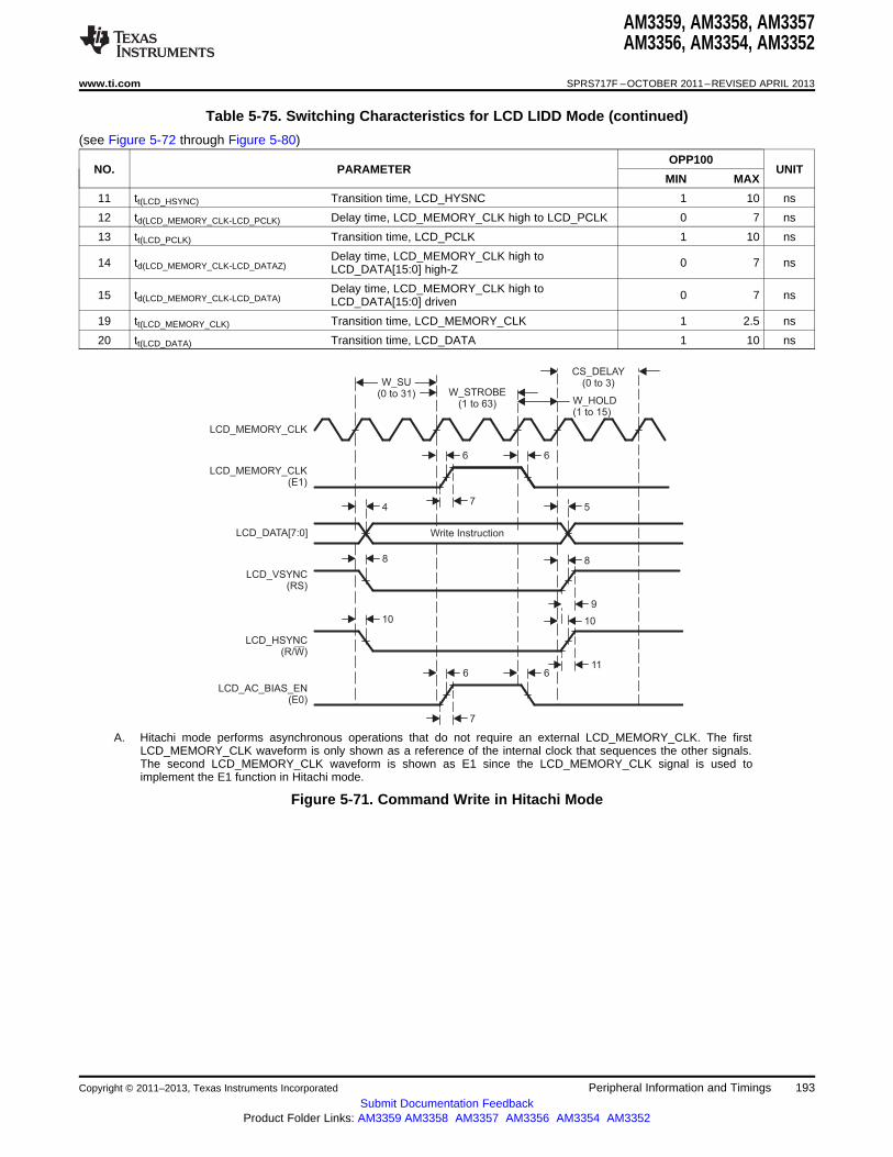
LCD_AC_BIAS_EN(E0)
W_SU(0 to 31) W_STROBE
(1 to 63) W_HOLD(1 to 15)
CS_DELAY(0 to 3)
LCD_MEMORY_CLK
4
Write Instruction
5
10
6
LCD_D [7:0]ATA
LCD_VSYNC(RS)
LCD_HSYNC(R/ )W
LCD_MEMORY_CLK(E1)
6
7
10
11
6 6
7
8 8
9
AM3359, AM3358, AM3357AM3356, AM3354, AM3352
www.ti.com SPRS717F –OCTOBER 2011–REVISED APRIL 2013
Table 5-75. Switching Characteristics for LCD LIDD Mode (continued)
(see Figure 5-72 through Figure 5-80)
OPP100NO. PARAMETER UNIT
MIN MAX
11 tt(LCD_HSYNC) Transition time, LCD_HYSNC 1 10 ns
12 td(LCD_MEMORY_CLK-LCD_PCLK) Delay time, LCD_MEMORY_CLK high to LCD_PCLK 0 7 ns
13 tt(LCD_PCLK) Transition time, LCD_PCLK 1 10 ns
Delay time, LCD_MEMORY_CLK high to14 td(LCD_MEMORY_CLK-LCD_DATAZ) 0 7 nsLCD_DATA[15:0] high-Z
Delay time, LCD_MEMORY_CLK high to15 td(LCD_MEMORY_CLK-LCD_DATA) 0 7 nsLCD_DATA[15:0] driven
19 tt(LCD_MEMORY_CLK) Transition time, LCD_MEMORY_CLK 1 2.5 ns
20 tt(LCD_DATA) Transition time, LCD_DATA 1 10 ns
A. Hitachi mode performs asynchronous operations that do not require an external LCD_MEMORY_CLK. The firstLCD_MEMORY_CLK waveform is only shown as a reference of the internal clock that sequences the other signals.The second LCD_MEMORY_CLK waveform is shown as E1 since the LCD_MEMORY_CLK signal is used toimplement the E1 function in Hitachi mode.
Figure 5-71. Command Write in Hitachi Mode
Copyright © 2011–2013, Texas Instruments Incorporated Peripheral Information and Timings 193Submit Documentation Feedback
Product Folder Links: AM3359 AM3358 AM3357 AM3356 AM3354 AM3352

R_SU(0 to 31)
R_STROBE(1 to 63)
R_HOLD(1 to 15) CS_DELAY
(0 to 3)
14 1617
15
8Read Command
LCD_AC_BIAS_EN(E0)
LCD_MEMORY_CLK
LCD_DATA[15:0]
LCD_VSYNC(RS)
LCD_HSYNC(R/ )W
LCD_MEMORY_CLK(E1)
6
7
6
6
7
6
18 8
9
LCD_AC_BIAS_EN(E0)
W_SU(0 to 31) W_STROBE
(1 to 63) W_HOLD(1 to 15)
CS_DELAY(0 to 3)
LCD_MEMORY_CLK
4
Write Data
5
10
6
LCD_D [15:0]ATA
LCD_VSYNC(RS)
LCD_HSYNC(R/ )W
LCD_MEMORY_CLK(E1)
20
6
7
10
11
6 6
7
AM3359, AM3358, AM3357AM3356, AM3354, AM3352
SPRS717F –OCTOBER 2011–REVISED APRIL 2013 www.ti.com
A. Hitachi mode performs asynchronous operations that do not require an external LCD_MEMORY_CLK. The firstLCD_MEMORY_CLK waveform is only shown as a reference of the internal clock that sequences the other signals.The second LCD_MEMORY_CLK waveform is shown as E1 since the LCD_MEMORY_CLK signal is used toimplement the E1 function in Hitachi mode.
Figure 5-72. Data Write in Hitachi Mode
A. Hitachi mode performs asynchronous operations that do not require an external LCD_MEMORY_CLK. The firstLCD_MEMORY_CLK waveform is only shown as a reference of the internal clock that sequences the other signals.The second LCD_MEMORY_CLK waveform is shown as E1 since the LCD_MEMORY_CLK signal is used toimplement the E1 function in Hitachi mode.
Figure 5-73. Command Read in Hitachi Mode
194 Peripheral Information and Timings Copyright © 2011–2013, Texas Instruments Incorporated
Submit Documentation FeedbackProduct Folder Links: AM3359 AM3358 AM3357 AM3356 AM3354 AM3352
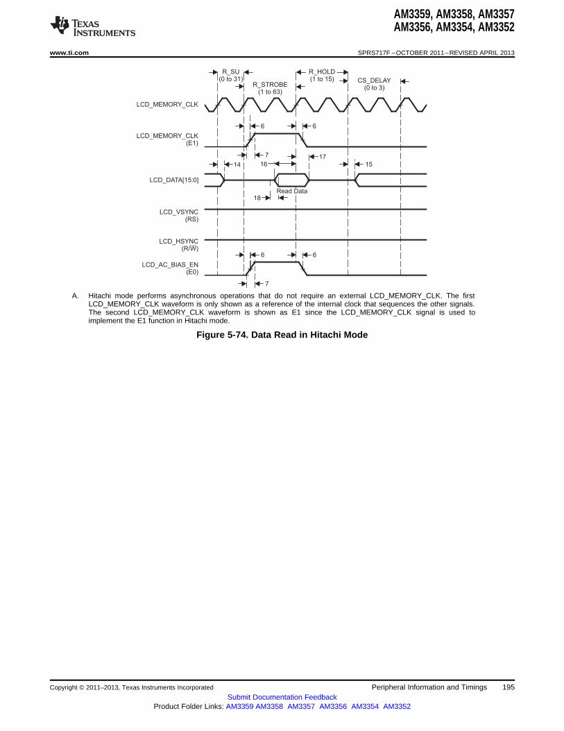
R_SU(0 to 31)
R_STROBE(1 to 63)
R_HOLD(1 to 15) CS_DELAY
(0 to 3)
14 1617
15
Read Data
LCD_AC_BIAS_EN(E0)
LCD_MEMORY_CLK
LCD_D [15:0]ATA
LCD_VSYNC(RS)
LCD_HSYNC(R/ )W
LCD_MEMORY_CLK(E1)
6
7
6
6
7
6
18
AM3359, AM3358, AM3357AM3356, AM3354, AM3352
www.ti.com SPRS717F –OCTOBER 2011–REVISED APRIL 2013
A. Hitachi mode performs asynchronous operations that do not require an external LCD_MEMORY_CLK. The firstLCD_MEMORY_CLK waveform is only shown as a reference of the internal clock that sequences the other signals.The second LCD_MEMORY_CLK waveform is shown as E1 since the LCD_MEMORY_CLK signal is used toimplement the E1 function in Hitachi mode.
Figure 5-74. Data Read in Hitachi Mode
Copyright © 2011–2013, Texas Instruments Incorporated Peripheral Information and Timings 195Submit Documentation Feedback
Product Folder Links: AM3359 AM3358 AM3357 AM3356 AM3354 AM3352
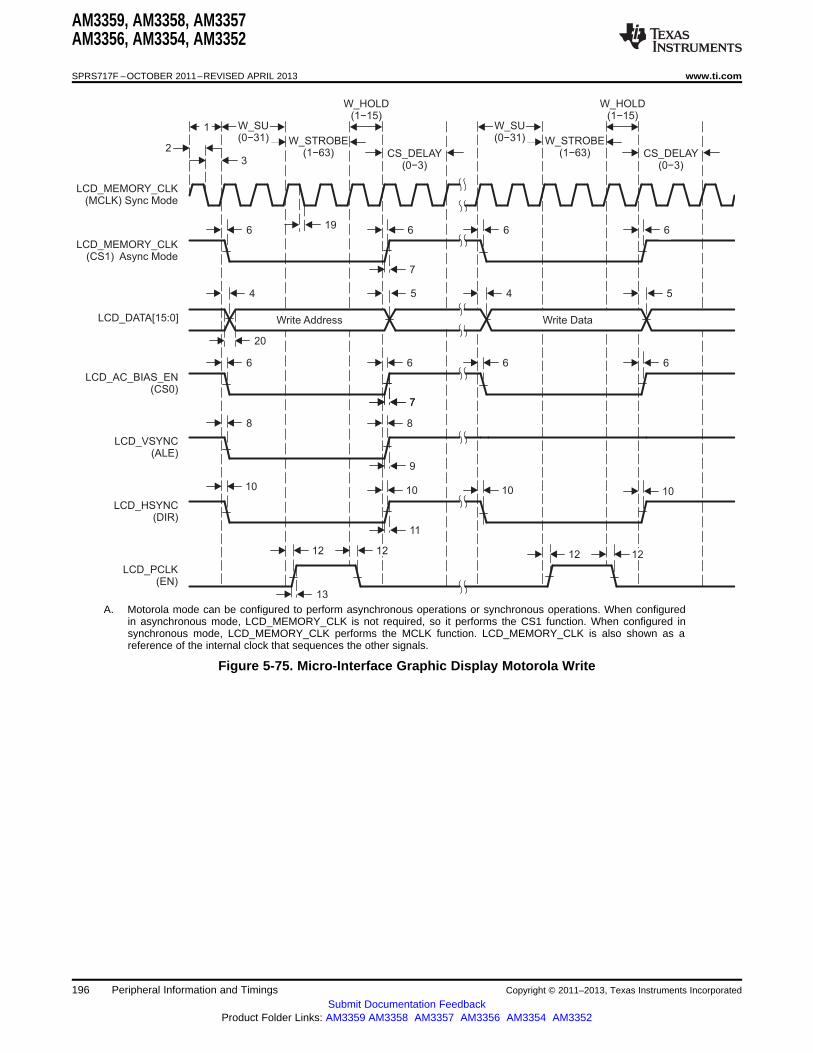
LCD_D [15:0]ATA
LCD_AC_BIAS_EN(CS0)
LCD_VSYNC(ALE)
LCD_HSYNC(DIR)
LCD_MEMORY_CLK(MCLK) Sync Mode
LCD_PCLK(EN)
W_SU(0−31) W_STROBE
(1−63)
W_HOLD(1−15)
CS_DELAY(0−3)
Write Address Write Data
LCD_MEMORY_CLK(CS1) Async Mode
6 6 619
4
20
6
8
10
12 12
6 6
8
10
77
9
11
13
12
10 10
6
5 4 5
6
W_SU(0−31) W_STROBE
(1−63)
W_HOLD(1−15)
CS_DELAY(0−3)
1
3
2
12
7
AM3359, AM3358, AM3357AM3356, AM3354, AM3352
SPRS717F –OCTOBER 2011–REVISED APRIL 2013 www.ti.com
A. Motorola mode can be configured to perform asynchronous operations or synchronous operations. When configuredin asynchronous mode, LCD_MEMORY_CLK is not required, so it performs the CS1 function. When configured insynchronous mode, LCD_MEMORY_CLK performs the MCLK function. LCD_MEMORY_CLK is also shown as areference of the internal clock that sequences the other signals.
Figure 5-75. Micro-Interface Graphic Display Motorola Write
196 Peripheral Information and Timings Copyright © 2011–2013, Texas Instruments Incorporated
Submit Documentation FeedbackProduct Folder Links: AM3359 AM3358 AM3357 AM3356 AM3354 AM3352
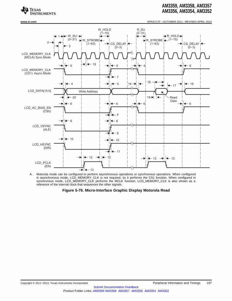
LCD_D [15:0]ATA
LCD_AC_BIAS_EN(CS0)
LCD_VSYNC(ALE)
LCD_HSYNC(DIR)
LCD_MEMORY_CLK(MCLK) Sync Mode
LCD_PCLK(EN)
W_SU(0−31) W_STROBE
(1−63)
W_HOLD(1−15)
CS_DELAY(0−3)
Write Address
ReadData
LCD_MEMORY_CLK(CS1) Async Mode
6 6 619
4
20
6
8
10
12 12
6 6
8
10
77
9
11
13
12 12
6
5 14 15
6
R_SU(0−31)
R_STROBE(1−63) CS_DELAY
(0−3)
R_HOLD(1−15)
16
18
17
1
3
2
7
AM3359, AM3358, AM3357AM3356, AM3354, AM3352
www.ti.com SPRS717F –OCTOBER 2011–REVISED APRIL 2013
A. Motorola mode can be configured to perform asynchronous operations or synchronous operations. When configuredin asynchronous mode, LCD_MEMORY_CLK is not required, so it performs the CS1 function. When configured insynchronous mode, LCD_MEMORY_CLK performs the MCLK function. LCD_MEMORY_CLK is also shown as areference of the internal clock that sequences the other signals.
Figure 5-76. Micro-Interface Graphic Display Motorola Read
Copyright © 2011–2013, Texas Instruments Incorporated Peripheral Information and Timings 197Submit Documentation Feedback
Product Folder Links: AM3359 AM3358 AM3357 AM3356 AM3354 AM3352
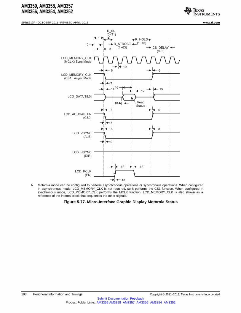
LCD_D [15:0]ATA
LCD_AC_BIAS_EN(CS0)
LCD_VSYNC(ALE)
LCD_HSYNC(DIR)
LCD_MEMORY_CLK(MCLK) Sync Mode
LCD_PCLK(EN)
ReadStatus
LCD_MEMORY_CLK(CS1) Async Mode
6
6
12 12
6
14 15
6
R_SU(0−31)
R_STROBE(1−63) CS_DELAY
(0−3)
R_HOLD(1−15)
16
18
17
8 8
13
9
7
1
3
2
7
19
AM3359, AM3358, AM3357AM3356, AM3354, AM3352
SPRS717F –OCTOBER 2011–REVISED APRIL 2013 www.ti.com
A. Motorola mode can be configured to perform asynchronous operations or synchronous operations. When configuredin asynchronous mode, LCD_MEMORY_CLK is not required, so it performs the CS1 function. When configured insynchronous mode, LCD_MEMORY_CLK performs the MCLK function. LCD_MEMORY_CLK is also shown as areference of the internal clock that sequences the other signals.
Figure 5-77. Micro-Interface Graphic Display Motorola Status
198 Peripheral Information and Timings Copyright © 2011–2013, Texas Instruments Incorporated
Submit Documentation FeedbackProduct Folder Links: AM3359 AM3358 AM3357 AM3356 AM3354 AM3352
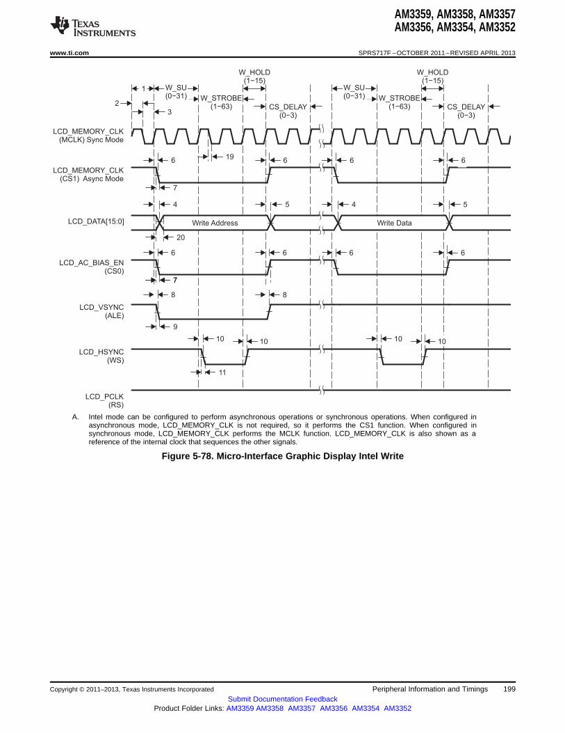
LCD_D [15:0]ATA
LCD_AC_BIAS_EN(CS0)
LCD_VSYNC(ALE)
LCD_HSYNC(WS)
LCD_MEMORY_CLK(MCLK) Sync Mode
LCD_PCLK(RS)
W_SU(0−31) W_STROBE
(1−63)
W_HOLD(1−15)
CS_DELAY(0−3)
Write Address Write Data
LCD_MEMORY_CLK(CS1) Async Mode
6 6 619
4
20
6
8
10
6 6
8
10
77
6
5 4 5
6
W_SU(0−31) W_STROBE
(1−63)
W_HOLD(1−15)
CS_DELAY(0−3)
1
3
2
9
11
10 10
7
AM3359, AM3358, AM3357AM3356, AM3354, AM3352
www.ti.com SPRS717F –OCTOBER 2011–REVISED APRIL 2013
A. Intel mode can be configured to perform asynchronous operations or synchronous operations. When configured inasynchronous mode, LCD_MEMORY_CLK is not required, so it performs the CS1 function. When configured insynchronous mode, LCD_MEMORY_CLK performs the MCLK function. LCD_MEMORY_CLK is also shown as areference of the internal clock that sequences the other signals.
Figure 5-78. Micro-Interface Graphic Display Intel Write
Copyright © 2011–2013, Texas Instruments Incorporated Peripheral Information and Timings 199Submit Documentation Feedback
Product Folder Links: AM3359 AM3358 AM3357 AM3356 AM3354 AM3352

LCD_D [15:0]ATA
LCD_AC_BIAS_EN(CS0)
LCD_VSYNC(ALE)
LCD_HSYNC(WS)
LCD_MEMORY_CLK(MCLK) Sync Mode
LCD_PCLK(RS)
W_SU(0−31) W_STROBE
(1−63)
W_HOLD(1−15)
CS_DELAY(0−3)
Write Address
ReadData
LCD_MEMORY_CLK(CS1) Async Mode
6 6 619
4
20
6
8
10
6 6
8
10
77
12 12
6
5 14 15
6
R_SU(0−31)
R_STROBE(1−63) CS_DELAY
(0−3)
R_HOLD(1−15)
16
18
17
1
3
2
9
11
13
7
AM3359, AM3358, AM3357AM3356, AM3354, AM3352
SPRS717F –OCTOBER 2011–REVISED APRIL 2013 www.ti.com
A. Intel mode can be configured to perform asynchronous operations or synchronous operations. When configured inasynchronous mode, LCD_MEMORY_CLK is not required, so it performs the CS1 function. When configured insynchronous mode, LCD_MEMORY_CLK performs the MCLK function. LCD_MEMORY_CLK is also shown as areference of the internal clock that sequences the other signals.
Figure 5-79. Micro-Interface Graphic Display Intel Read
200 Peripheral Information and Timings Copyright © 2011–2013, Texas Instruments Incorporated
Submit Documentation FeedbackProduct Folder Links: AM3359 AM3358 AM3357 AM3356 AM3354 AM3352
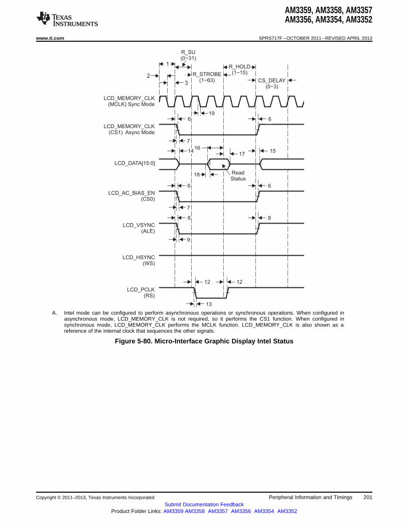
LCD_D [15:0]ATA
LCD_AC_BIAS_EN(CS0)
LCD_VSYNC(ALE)
LCD_HSYNC(WS)
LCD_MEMORY_CLK(MCLK) Sync Mode
LCD_PCLK(RS)
ReadStatus
LCD_MEMORY_CLK(CS1) Async Mode
6
6
12 12
6
14 15
6
R_SU(0−31)
R_STROBE(1−63) CS_DELAY
(0−3)
R_HOLD(1−15)
16
18
17
8 8
13
9
7
1
3
2
19
7
AM3359, AM3358, AM3357AM3356, AM3354, AM3352
www.ti.com SPRS717F –OCTOBER 2011–REVISED APRIL 2013
A. Intel mode can be configured to perform asynchronous operations or synchronous operations. When configured inasynchronous mode, LCD_MEMORY_CLK is not required, so it performs the CS1 function. When configured insynchronous mode, LCD_MEMORY_CLK performs the MCLK function. LCD_MEMORY_CLK is also shown as areference of the internal clock that sequences the other signals.
Figure 5-80. Micro-Interface Graphic Display Intel Status
Copyright © 2011–2013, Texas Instruments Incorporated Peripheral Information and Timings 201Submit Documentation Feedback
Product Folder Links: AM3359 AM3358 AM3357 AM3356 AM3354 AM3352
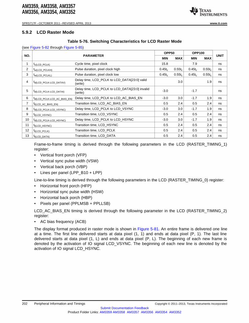
AM3359, AM3358, AM3357AM3356, AM3354, AM3352
SPRS717F –OCTOBER 2011–REVISED APRIL 2013 www.ti.com
5.9.2 LCD Raster Mode
Table 5-76. Switching Characteristics for LCD Raster Mode(see Figure 5-82 through Figure 5-85)
OPP50 OPP100NO. PARAMETER UNIT
MIN MAX MIN MAX
1 tc(LCD_PCLK) Cycle time, pixel clock 15.8 7.9 ns
2 tw(LCD_PCLKH) Pulse duration, pixel clock high 0.45tc 0.55tc 0.45tc 0.55tc ns
3 tw(LCD_PCLKL) Pulse duration, pixel clock low 0.45tc 0.55tc 0.45tc 0.55tc ns
Delay time, LCD_PCLK to LCD_DATA[23:0] valid4 td(LCD_PCLK-LCD_DATAV) 3.0 1.9 ns(write)
Delay time, LCD_PCLK to LCD_DATA[23:0] invalid5 td(LCD_PCLK-LCD_DATAI) -3.0 -1.7 ns(write)
6 td(LCD_PCLK-LCD_AC_BIAS_EN) Delay time, LCD_PCLK to LCD_AC_BIAS_EN -3.0 3.0 -1.7 1.9 ns
7 tt(LCD_AC_BIAS_EN) Transition time, LCD_AC_BIAS_EN 0.5 2.4 0.5 2.4 ns
8 td(LCD_PCLK-LCD_VSYNC) Delay time, LCD_PCLK to LCD_VSYNC -3.0 3.0 -1.7 1.9 ns
9 tt(LCD_VSYNC) Transition time, LCD_VSYNC 0.5 2.4 0.5 2.4 ns
10 td(LCD_PCLK-LCD_HSYNC) Delay time, LCD_PCLK to LCD_HSYNC -3.0 3.0 -1.7 1.9 ns
11 tt(LCD_HSYNC) Transition time, LCD_HSYNC 0.5 2.4 0.5 2.4 ns
12 tt(LCD_PCLK) Transition time, LCD_PCLK 0.5 2.4 0.5 2.4 ns
13 tt(LCD_DATA) Transition time, LCD_DATA 0.5 2.4 0.5 2.4 ns
Frame-to-frame timing is derived through the following parameters in the LCD (RASTER_TIMING_1)register:• Vertical front porch (VFP)• Vertical sync pulse width (VSW)• Vertical back porch (VBP)• Lines per panel (LPP_B10 + LPP)
Line-to-line timing is derived through the following parameters in the LCD (RASTER_TIMING_0) register:• Horizontal front porch (HFP)• Horizontal sync pulse width (HSW)• Horizontal back porch (HBP)• Pixels per panel (PPLMSB + PPLLSB)
LCD_AC_BIAS_EN timing is derived through the following parameter in the LCD (RASTER_TIMING_2)register:• AC bias frequency (ACB)
The display format produced in raster mode is shown in Figure 5-81. An entire frame is delivered one lineat a time. The first line delivered starts at data pixel (1, 1) and ends at data pixel (P, 1). The last linedelivered starts at data pixel (1, L) and ends at data pixel (P, L). The beginning of each new frame isdenoted by the activation of IO signal LCD_VSYNC. The beginning of each new line is denoted by theactivation of IO signal LCD_HSYNC.
202 Peripheral Information and Timings Copyright © 2011–2013, Texas Instruments Incorporated
Submit Documentation FeedbackProduct Folder Links: AM3359 AM3358 AM3357 AM3356 AM3354 AM3352

LCD
1, 1
1, 2 2, 2
1, 3
P, 1P−1,
1P−2,
1
P, 2P−1,
2
P, 3
1, L
1,L−2
3, L2, L P, L
P−1,L−1
P,L−1
P−1,L
P,L−2
P−2,L
Data Pixels (From 1 to P)D
ata
Lin
es (
Fro
m 1
to L
)
2, 1 3, 1
1,L−1
2,L−1
AM3359, AM3358, AM3357AM3356, AM3354, AM3352
www.ti.com SPRS717F –OCTOBER 2011–REVISED APRIL 2013
Figure 5-81. LCD Raster-Mode Display Format
Copyright © 2011–2013, Texas Instruments Incorporated Peripheral Information and Timings 203Submit Documentation Feedback
Product Folder Links: AM3359 AM3358 AM3357 AM3356 AM3354 AM3352
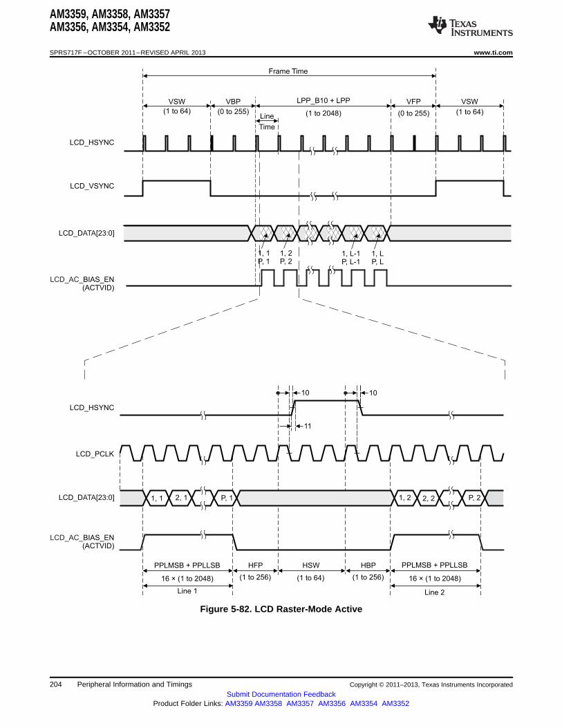
LCD_HSYNC
LCD_VSYNC
(1 to 64)
VSW
(1 to 64)
VSW
(0 to 255)
VFP
(1 to 2048)
Frame Time
LPP_B10 + LPP
(0 to 255)
LCD_D [23:0]ATA
1, 1P, 1
1, 2P, 2
1, LP, L
1, L-1P, L-1
Line
Time
LCD_AC_BIAS_EN(ACTVID)
VBP
LCD_HSYNC
10 10
LCD_PCLK
LCD_D [23:0]ATA 1, 1 2, 2 P, 2P, 12, 1 1, 2
PPLMSB + PPLLSB
16 × (1 to 2048)
HBP
(1 to 256)
Line 1
(1 to 256)
HFP
(1 to 64)
HSW PPLMSB + PPLLSB
16 × (1 to 2048)
Line 2
LCD_AC_BIAS_EN(ACTVID)
11
AM3359, AM3358, AM3357AM3356, AM3354, AM3352
SPRS717F –OCTOBER 2011–REVISED APRIL 2013 www.ti.com
Figure 5-82. LCD Raster-Mode Active
204 Peripheral Information and Timings Copyright © 2011–2013, Texas Instruments Incorporated
Submit Documentation FeedbackProduct Folder Links: AM3359 AM3358 AM3357 AM3356 AM3354 AM3352
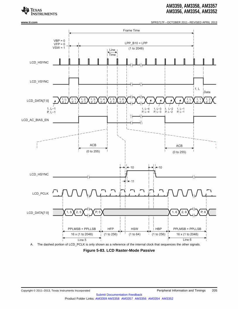
LCD_HSYNC
LCD_VSYNC
(1 to 2048)
Frame Time
LPP_B10 + LPP
LCD_D [7:0]ATA
1, L−2P, L−2
1, L−4P, L−4
Line
Time
LCD_HSYNC
10 10
LCD_PCLK
LCD_D [7:0]ATA 1, 5 2, 6 P, 6P, 52, 5 1, 6
PPLMSB + PPLLSB
16 x (1 to 2048)
HBP
(1 to 256)
Line 5
HFP
(1 to 64)
HSW PPLMSB + PPLLSB
16 x (1 to 2048)
Line 6
1, 1:P, 1
1, 5:P, 5
1, L−1P, L−1
1, L
1, L−1P, L−1
1, L−3P, L−3
VBP = 0VFP = 0
VSW = 1
Data
LCD_AC_BIAS_EN
ACB
(0 to 255)
ACB
(0 to 255)
1, 4:P, 4
1, 3:P, 3
1, 2:P, 2
1, L:P, L
1, 6:P, 6
1, 2P, 2
1, 1P, 1
1, LP, L
(1 to 256)
11
AM3359, AM3358, AM3357AM3356, AM3354, AM3352
www.ti.com SPRS717F –OCTOBER 2011–REVISED APRIL 2013
A. The dashed portion of LCD_PCLK is only shown as a reference of the internal clock that sequences the other signals.
Figure 5-83. LCD Raster-Mode Passive
Copyright © 2011–2013, Texas Instruments Incorporated Peripheral Information and Timings 205Submit Documentation Feedback
Product Folder Links: AM3359 AM3358 AM3357 AM3356 AM3354 AM3352

LCD_HSYNC
LCD_PCLK(active mode)
LCD_D [23:0](active mode)
ATA1, L P, L2, L
PPLMSB + PPLLSB
16 x (1 to 2048)
HBP
(1 to 256)
Line L
(1 to 256)
HFP
(1 to 64)
HSW
Line 1 (Passive Only)
LCD_VSYNC
LCD_PCLK(passive mode)
LCD_AC_BIAS_EN
LCD_D [7:0](passive mode)
ATA1, L 2, 1 P, 1P, L2, L 1, 1
10 10
8
6
4 5
1
2 3
VBP = 0VFP = 0
VWS = 1
1
2 3
4 5
PPLMSB + PPLLSB
16 x (1 to 2048)
7
9
11
AM3359, AM3358, AM3357AM3356, AM3354, AM3352
SPRS717F –OCTOBER 2011–REVISED APRIL 2013 www.ti.com
A. The dashed portion of LCD_PCLK is only shown as a reference of the internal clock that sequences the other signals.
Figure 5-84. LCD Raster-Mode Control Signal Activation
206 Peripheral Information and Timings Copyright © 2011–2013, Texas Instruments Incorporated
Submit Documentation FeedbackProduct Folder Links: AM3359 AM3358 AM3357 AM3356 AM3354 AM3352
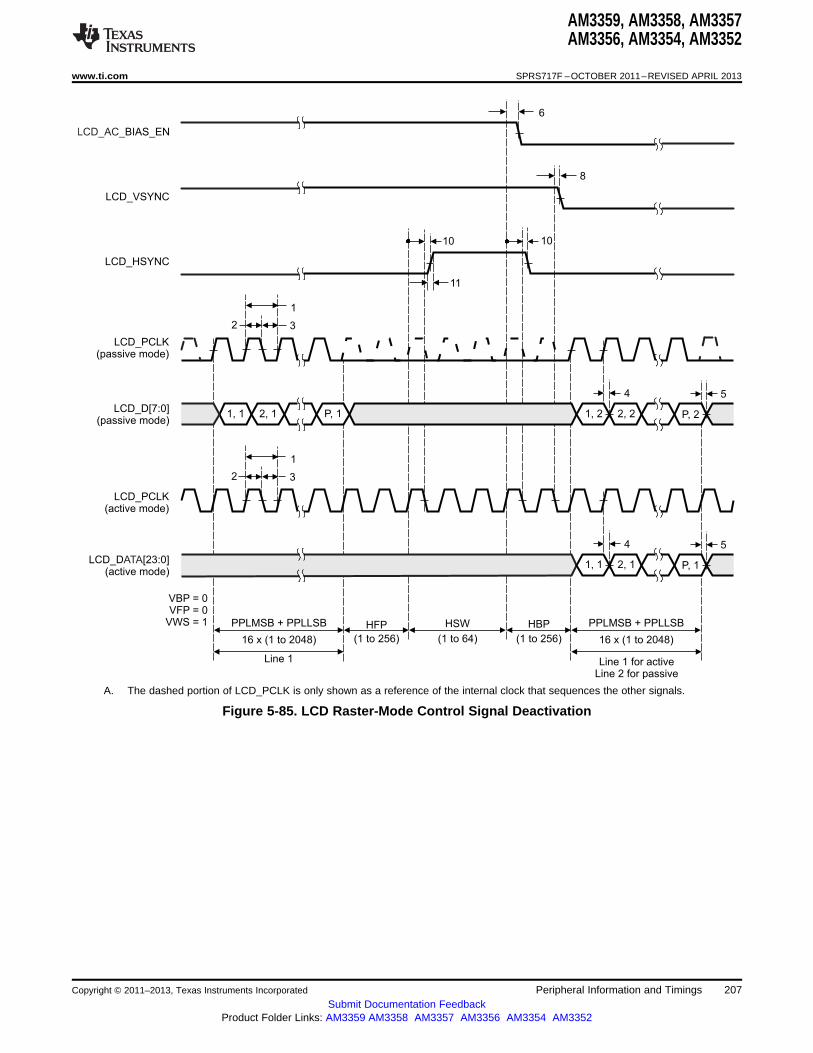
LCD_HSYNC
LCD_PCLK(active mode)
LCD_D [23:0](active mode)
ATA
PPLMSB + PPLLSB
16 x (1 to 2048)
HBP
(1 to 256)
Line 1
(1 to 256)
HFP
(1 to 64)
HSW
Line 1 for activeLine 2 for passive
LCD_VSYNC
LCD_PCLK(passive mode)
LCD_AC_BIAS_EN
LCD_D[7:0](passive mode)
1, 1 2, 2 P, 2P, 12, 1 1, 2
10 10
8
6
4 5
1
2 3
VBP = 0VFP = 0
VWS = 1 PPLMSB + PPLLSB
16 x (1 to 2048)
11
1
2 3
2, 1 P, 11, 1
4 5
AM3359, AM3358, AM3357AM3356, AM3354, AM3352
www.ti.com SPRS717F –OCTOBER 2011–REVISED APRIL 2013
A. The dashed portion of LCD_PCLK is only shown as a reference of the internal clock that sequences the other signals.
Figure 5-85. LCD Raster-Mode Control Signal Deactivation
Copyright © 2011–2013, Texas Instruments Incorporated Peripheral Information and Timings 207Submit Documentation Feedback
Product Folder Links: AM3359 AM3358 AM3357 AM3356 AM3354 AM3352

AM3359, AM3358, AM3357AM3356, AM3354, AM3352
SPRS717F –OCTOBER 2011–REVISED APRIL 2013 www.ti.com
5.10 Multichannel Audio Serial Port (McASP)
The multichannel audio serial port (McASP) functions as a general-purpose audio serial port optimized forthe needs of multichannel audio applications. The McASP is useful for time-division multiplexed (TDM)stream, Inter-Integrated Sound (I2S) protocols, and inter-component digital audio interface transmission(DIT).
5.10.1 McASP Device-Specific Information
The device includes two multichannel audio serial port (McASP) interface peripherals (McASP0 andMcASP1). The McASP module consists of a transmit and receive section. These sections can operatecompletely independently with different data formats, separate master clocks, bit clocks, and frame syncsor, alternatively, the transmit and receive sections may be synchronized. The McASP module alsoincludes shift registers that may be configured to operate as either transmit data or receive data.
The transmit section of the McASP can transmit data in either a time-division-multiplexed (TDM)synchronous serial format or in a digital audio interface (DIT) format where the bit stream is encoded forSPDIF, AES-3, IEC-60958, CP-430 transmission. The receive section of the McASP peripheral supportsthe TDM synchronous serial format.
The McASP module can support one transmit data format (either a TDM format or DIT format) and onereceive format at a time. All transmit shift registers use the same format and all receive shift registers usethe same format; however, the transmit and receive formats need not be the same. Both the transmit andreceive sections of the McASP also support burst mode, which is useful for non-audio data (for example,passing control information between two devices).
The McASP peripheral has additional capability for flexible clock generation and error detection/handling,as well as error management.
The device McASP0 and McASP1 modules have up to four serial data pins each. The McASP FIFO sizeis 256 bytes and two DMA and two interrupt requests are supported. Buffers are used transparently tobetter manage DMA, which can be leveraged to manage data flow more efficiently.
For more detailed information on and the functionality of the McASP peripheral, see the MultichannelAudio Serial Port (McASP) section of the AM335x ARM Cortex-A8 Microprocessors (MPUs) TechnicalReference Manual (literature number SPRUH73).
208 Peripheral Information and Timings Copyright © 2011–2013, Texas Instruments Incorporated
Submit Documentation FeedbackProduct Folder Links: AM3359 AM3358 AM3357 AM3356 AM3354 AM3352
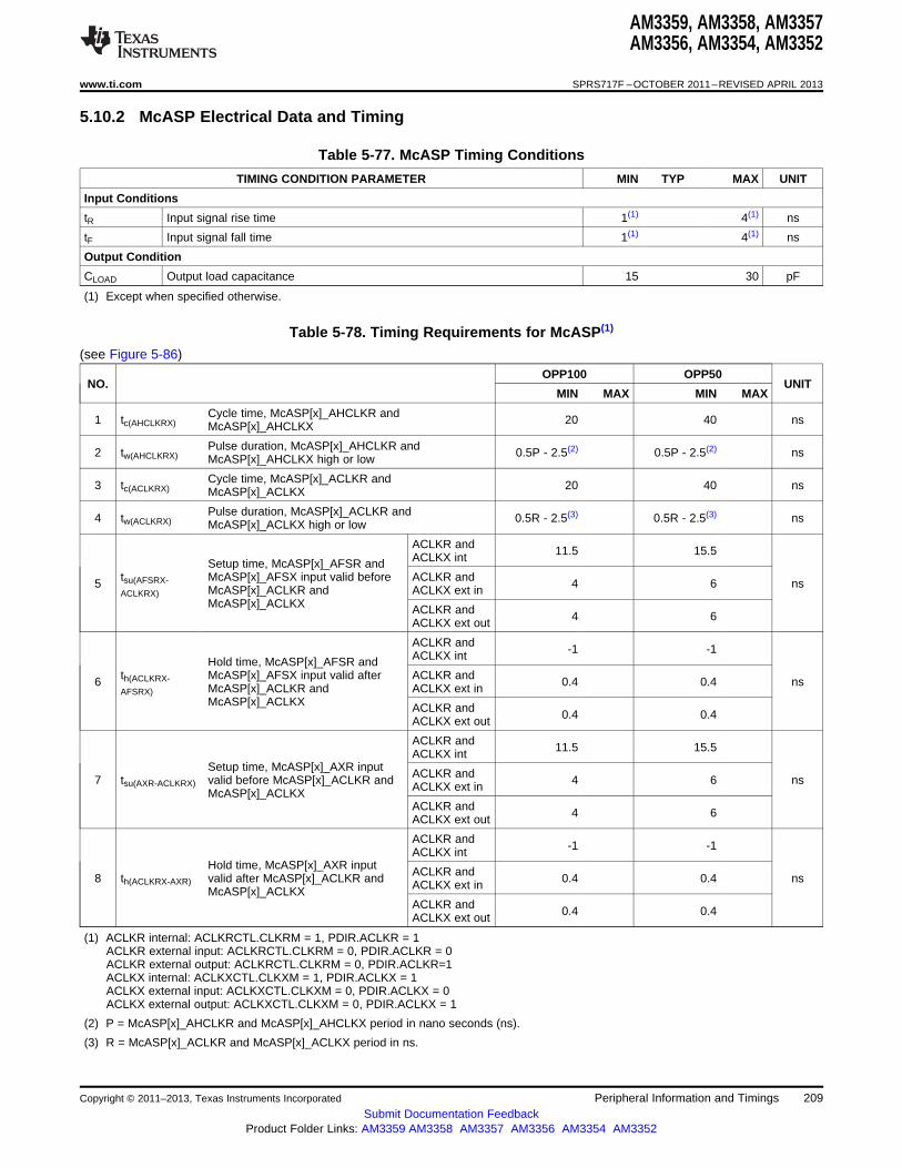
AM3359, AM3358, AM3357AM3356, AM3354, AM3352
www.ti.com SPRS717F –OCTOBER 2011–REVISED APRIL 2013
5.10.2 McASP Electrical Data and Timing
Table 5-77. McASP Timing Conditions
TIMING CONDITION PARAMETER MIN TYP MAX UNIT
Input Conditions
tR Input signal rise time 1(1) 4(1) ns
tF Input signal fall time 1(1) 4(1) ns
Output Condition
CLOAD Output load capacitance 15 30 pF
(1) Except when specified otherwise.
Table 5-78. Timing Requirements for McASP(1)
(see Figure 5-86)
OPP100 OPP50NO. UNIT
MIN MAX MIN MAX
Cycle time, McASP[x]_AHCLKR and1 tc(AHCLKRX) 20 40 nsMcASP[x]_AHCLKX
Pulse duration, McASP[x]_AHCLKR and2 tw(AHCLKRX) 0.5P - 2.5(2) 0.5P - 2.5(2) nsMcASP[x]_AHCLKX high or low
Cycle time, McASP[x]_ACLKR and3 tc(ACLKRX) 20 40 nsMcASP[x]_ACLKX
Pulse duration, McASP[x]_ACLKR and4 tw(ACLKRX) 0.5R - 2.5(3) 0.5R - 2.5(3) nsMcASP[x]_ACLKX high or low
ACLKR and 11.5 15.5ACLKX intSetup time, McASP[x]_AFSR andtsu(AFSRX- McASP[x]_AFSX input valid before ACLKR and5 4 6 nsACLKRX) McASP[x]_ACLKR and ACLKX ext in
McASP[x]_ACLKX ACLKR and 4 6ACLKX ext out
ACLKR and -1 -1ACLKX intHold time, McASP[x]_AFSR andth(ACLKRX- McASP[x]_AFSX input valid after ACLKR and6 0.4 0.4 nsAFSRX) McASP[x]_ACLKR and ACLKX ext in
McASP[x]_ACLKX ACLKR and 0.4 0.4ACLKX ext out
ACLKR and 11.5 15.5ACLKX intSetup time, McASP[x]_AXR input ACLKR and7 tsu(AXR-ACLKRX) valid before McASP[x]_ACLKR and 4 6 nsACLKX ext inMcASP[x]_ACLKX
ACLKR and 4 6ACLKX ext out
ACLKR and -1 -1ACLKX intHold time, McASP[x]_AXR input ACLKR and8 th(ACLKRX-AXR) valid after McASP[x]_ACLKR and 0.4 0.4 nsACLKX ext inMcASP[x]_ACLKX
ACLKR and 0.4 0.4ACLKX ext out
(1) ACLKR internal: ACLKRCTL.CLKRM = 1, PDIR.ACLKR = 1ACLKR external input: ACLKRCTL.CLKRM = 0, PDIR.ACLKR = 0ACLKR external output: ACLKRCTL.CLKRM = 0, PDIR.ACLKR=1ACLKX internal: ACLKXCTL.CLKXM = 1, PDIR.ACLKX = 1ACLKX external input: ACLKXCTL.CLKXM = 0, PDIR.ACLKX = 0ACLKX external output: ACLKXCTL.CLKXM = 0, PDIR.ACLKX = 1
(2) P = McASP[x]_AHCLKR and McASP[x]_AHCLKX period in nano seconds (ns).
(3) R = McASP[x]_ACLKR and McASP[x]_ACLKX period in ns.
Copyright © 2011–2013, Texas Instruments Incorporated Peripheral Information and Timings 209Submit Documentation Feedback
Product Folder Links: AM3359 AM3358 AM3357 AM3356 AM3354 AM3352
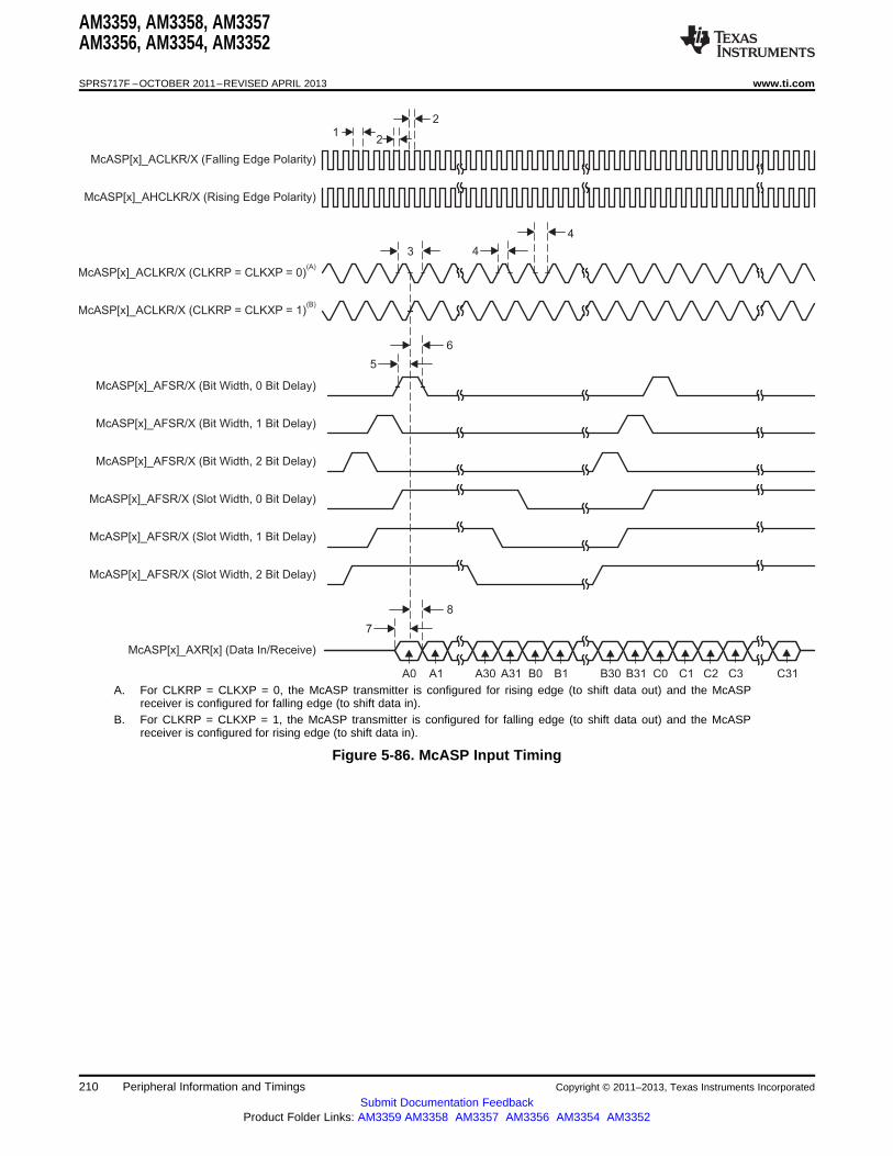
8
7
4
43
2
21
A0 A1 B0 B1A30 A31 B30 B31 C0 C1 C2 C3 C31
McASP[x]_ACLKR/X (Falling Edge Polarity)
McASP[x]_AHCLKR/X (Rising Edge Polarity)
McASP[x]_AFSR/X (Bit Width, 0 Bit Delay)
McASP[x]_AFSR/X (Bit Width, 1 Bit Delay)
McASP[x]_AFSR/X (Bit Width, 2 Bit Delay)
McASP[x]_AFSR/X (Slot Width, 0 Bit Delay)
McASP[x]_AFSR/X (Slot Width, 1 Bit Delay)
McASP[x]_AFSR/X (Slot Width, 2 Bit Delay)
McASP[x]_AXR[x] (Data In/Receive)
6
5
McASP[x]_ACLKR/X (CLKRP = CLKXP = 0)(A)
McASP[x]_ACLKR/X (CLKRP = CLKXP = 1)(B)
AM3359, AM3358, AM3357AM3356, AM3354, AM3352
SPRS717F –OCTOBER 2011–REVISED APRIL 2013 www.ti.com
A. For CLKRP = CLKXP = 0, the McASP transmitter is configured for rising edge (to shift data out) and the McASPreceiver is configured for falling edge (to shift data in).
B. For CLKRP = CLKXP = 1, the McASP transmitter is configured for falling edge (to shift data out) and the McASPreceiver is configured for rising edge (to shift data in).
Figure 5-86. McASP Input Timing
210 Peripheral Information and Timings Copyright © 2011–2013, Texas Instruments Incorporated
Submit Documentation FeedbackProduct Folder Links: AM3359 AM3358 AM3357 AM3356 AM3354 AM3352

AM3359, AM3358, AM3357AM3356, AM3354, AM3352
www.ti.com SPRS717F –OCTOBER 2011–REVISED APRIL 2013
Table 5-79. Switching Characteristics for McASP(1)
(see Figure 5-87)
OPP100 OPP50NO. UNIT
MIN MAX MIN MAX
Cycle time, McASP[x]_AHCLKR and9 tc(AHCLKRX) 20(2) 40 nsMcASP[x]_AHCLKX
Pulse duration, McASP[x]_AHCLKR and10 tw(AHCLKRX) 0.5P - 2.5(3) 0.5P - 2.5(3) nsMcASP[x]_AHCLKX high or low
Cycle time, McASP[x]_ACLKR and11 tc(ACLKRX) 20 40 nsMcASP[x]_ACLKX
Pulse duration, McASP[x]_ACLKR and12 tw(ACLKRX) 0.5P - 2.5(3) 0.5P - 2.5(3) nsMcASP[x]_ACLKX high or low
ACLKR andDelay time, McASP[x]_ACLKR and 0 6 0 6ACLKX intMcASP[x]_ACLKX transmit edge toMcASP[x]_AFSR and ACLKR and 2 13.5 2 18McASP[x]_AFSX output valid ACLKX ext in
13 td(ACLKRX-AFSRX) nsDelay time, McASP[x]_ACLKR andMcASP[x]_ACLKX transmit edge to ACLKR andMcASP[x]_AFSR and ACLKX ext 2 13.5 2 18McASP[x]_AFSX output valid with outPad Loopback
Delay time, McASP[x]_ACLKX ACLKX int 0 6 0 6transmit edge to McASP[x]_AXR
ACLKX ext in 2 13.5 2 18output valid14 td(ACLKX-AXR) ns
Delay time, McASP[x]_ACLKX ACLKX exttransmit edge to McASP[x]_AXR 2 13.5 2 18outoutput valid with Pad Loopback
Disable time, McASP[x]_ACLKX ACLKX int 0 6 0 6transmit edge to McASP[x]_AXR
ACLKX ext in 2 13.5 2 18output high impedance15 tdis(ACLKX-AXR) nsDisable time, McASP[x]_ACLKX
transmit edge to McASP[x]_AXR ACLKX ext 2 13.5 2 18output high impedance with Pad outLoopback
(1) ACLKR internal: ACLKRCTL.CLKRM = 1, PDIR.ACLKR = 1ACLKR external input: ACLKRCTL.CLKRM = 0, PDIR.ACLKR = 0ACLKR external output: ACLKRCTL.CLKRM = 0, PDIR.ACLKR = 1ACLKX internal: ACLKXCTL.CLKXM = 1, PDIR.ACLKX = 1ACLKX external input: ACLKXCTL.CLKXM = 0, PDIR.ACLKX = 0ACLKX external output: ACLKXCTL.CLKXM = 0, PDIR.ACLKX = 1
(2) 50 MHz
(3) P = AHCLKR and AHCLKX period.
Copyright © 2011–2013, Texas Instruments Incorporated Peripheral Information and Timings 211Submit Documentation Feedback
Product Folder Links: AM3359 AM3358 AM3357 AM3356 AM3354 AM3352
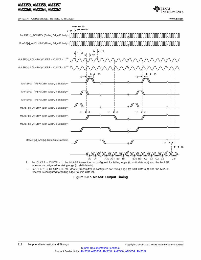
15
14
1313
12
1211
10
10
9
A0 A1 B0 B1A30 A31 B30 B31 C0 C1 C2 C3 C31
1313
13 1313
McASP[x]_ACLKR/X (Falling Edge Polarity)
McASP[x]_AHCLKR/X (Rising Edge Polarity)
McASP[x]_AFSR/X (Bit Width, 0 Bit Delay)
McASP[x]_AFSR/X (Bit Width, 1 Bit Delay)
McASP[x]_AFSR/X (Bit Width, 2 Bit Delay)
McASP[x]_AFSR/X (Slot Width, 0 Bit Delay)
McASP[x]_AFSR/X (Slot Width, 1 Bit Delay)
McASP[x]_AFSR/X (Slot Width, 2 Bit Delay)
McASP[x]_AXR[x] (Data Out/Transmit)
McASP[x]_ACLKR/X (CLKRP = CLKXP = 1)(A)
McASP[x]_ACLKR/X (CLKRP = CLKXP = 0)(B)
AM3359, AM3358, AM3357AM3356, AM3354, AM3352
SPRS717F –OCTOBER 2011–REVISED APRIL 2013 www.ti.com
A. For CLKRP = CLKXP = 1, the McASP transmitter is configured for falling edge (to shift data out) and the McASPreceiver is configured for rising edge (to shift data in).
B. For CLKRP = CLKXP = 0, the McASP transmitter is configured for rising edge (to shift data out) and the McASPreceiver is configured for falling edge (to shift data in).
Figure 5-87. McASP Output Timing
212 Peripheral Information and Timings Copyright © 2011–2013, Texas Instruments Incorporated
Submit Documentation FeedbackProduct Folder Links: AM3359 AM3358 AM3357 AM3356 AM3354 AM3352
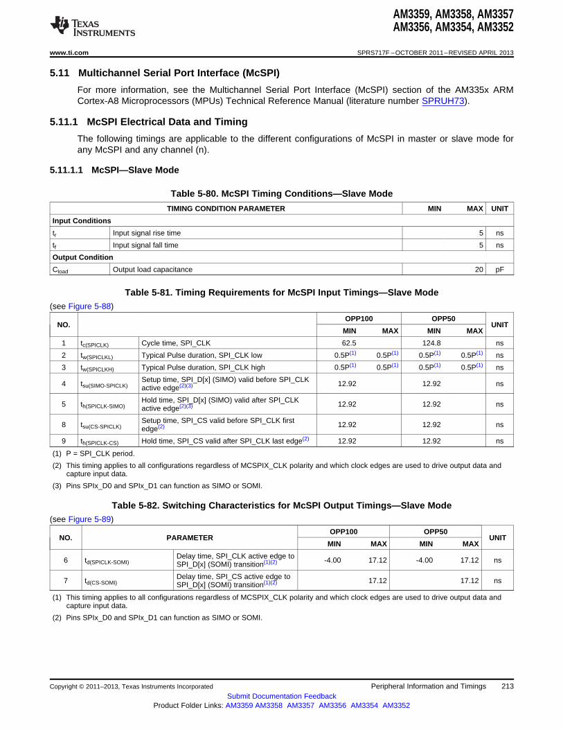
AM3359, AM3358, AM3357AM3356, AM3354, AM3352
www.ti.com SPRS717F –OCTOBER 2011–REVISED APRIL 2013
5.11 Multichannel Serial Port Interface (McSPI)
For more information, see the Multichannel Serial Port Interface (McSPI) section of the AM335x ARMCortex-A8 Microprocessors (MPUs) Technical Reference Manual (literature number SPRUH73).
5.11.1 McSPI Electrical Data and Timing
The following timings are applicable to the different configurations of McSPI in master or slave mode forany McSPI and any channel (n).
5.11.1.1 McSPI—Slave Mode
Table 5-80. McSPI Timing Conditions—Slave Mode
TIMING CONDITION PARAMETER MIN MAX UNIT
Input Conditions
tr Input signal rise time 5 ns
tf Input signal fall time 5 ns
Output Condition
Cload Output load capacitance 20 pF
Table 5-81. Timing Requirements for McSPI Input Timings—Slave Mode(see Figure 5-88)
OPP100 OPP50NO. UNIT
MIN MAX MIN MAX
1 tc(SPICLK) Cycle time, SPI_CLK 62.5 124.8 ns
2 tw(SPICLKL) Typical Pulse duration, SPI_CLK low 0.5P(1) 0.5P(1) 0.5P(1) 0.5P(1) ns
3 tw(SPICLKH) Typical Pulse duration, SPI_CLK high 0.5P(1) 0.5P(1) 0.5P(1) 0.5P(1) ns
Setup time, SPI_D[x] (SIMO) valid before SPI_CLK4 tsu(SIMO-SPICLK) 12.92 12.92 nsactive edge(2)(3)
Hold time, SPI_D[x] (SIMO) valid after SPI_CLK5 th(SPICLK-SIMO) 12.92 12.92 nsactive edge(2)(3)
Setup time, SPI_CS valid before SPI_CLK first8 tsu(CS-SPICLK) 12.92 12.92 nsedge(2)
9 th(SPICLK-CS) Hold time, SPI_CS valid after SPI_CLK last edge(2) 12.92 12.92 ns
(1) P = SPI_CLK period.
(2) This timing applies to all configurations regardless of MCSPIX_CLK polarity and which clock edges are used to drive output data andcapture input data.
(3) Pins SPIx_D0 and SPIx_D1 can function as SIMO or SOMI.
Table 5-82. Switching Characteristics for McSPI Output Timings—Slave Mode(see Figure 5-89)
OPP100 OPP50NO. PARAMETER UNIT
MIN MAX MIN MAX
Delay time, SPI_CLK active edge to6 td(SPICLK-SOMI) -4.00 17.12 -4.00 17.12 nsSPI_D[x] (SOMI) transition(1)(2)
Delay time, SPI_CS active edge to7 td(CS-SOMI) 17.12 17.12 nsSPI_D[x] (SOMI) transition(1)(2)
(1) This timing applies to all configurations regardless of MCSPIX_CLK polarity and which clock edges are used to drive output data andcapture input data.
(2) Pins SPIx_D0 and SPIx_D1 can function as SIMO or SOMI.
Copyright © 2011–2013, Texas Instruments Incorporated Peripheral Information and Timings 213Submit Documentation Feedback
Product Folder Links: AM3359 AM3358 AM3357 AM3356 AM3354 AM3352
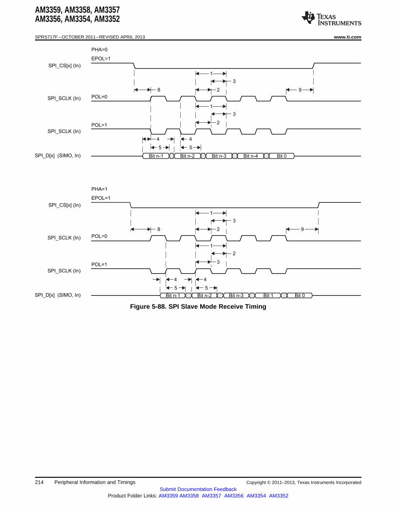
SPI_CS[x] (In)
SPI_SCLK (In)
SPI_SCLK (In)
SPI_D[x] (SIMO, In) Bit n-1 Bit n-2 Bit n-3 Bit n-4 Bit 0
PHA=0
EPOL=1
POL=0
POL=1
8
3
4
2
1
3
2
5
SPI_CS[x] (In)
SPI_SCLK (In)
SPI_SCLK (In)
SPI_D[x] ( )SIMO, In Bit n-1 Bit n-2 Bit n-3 Bit 1 Bit 0
PHA=1
EPOL=1
POL=0
POL=1
8
3
2
1
2
3
1
4
5
4
5 5
4
9
1
9
AM3359, AM3358, AM3357AM3356, AM3354, AM3352
SPRS717F –OCTOBER 2011–REVISED APRIL 2013 www.ti.com
Figure 5-88. SPI Slave Mode Receive Timing
214 Peripheral Information and Timings Copyright © 2011–2013, Texas Instruments Incorporated
Submit Documentation FeedbackProduct Folder Links: AM3359 AM3358 AM3357 AM3356 AM3354 AM3352
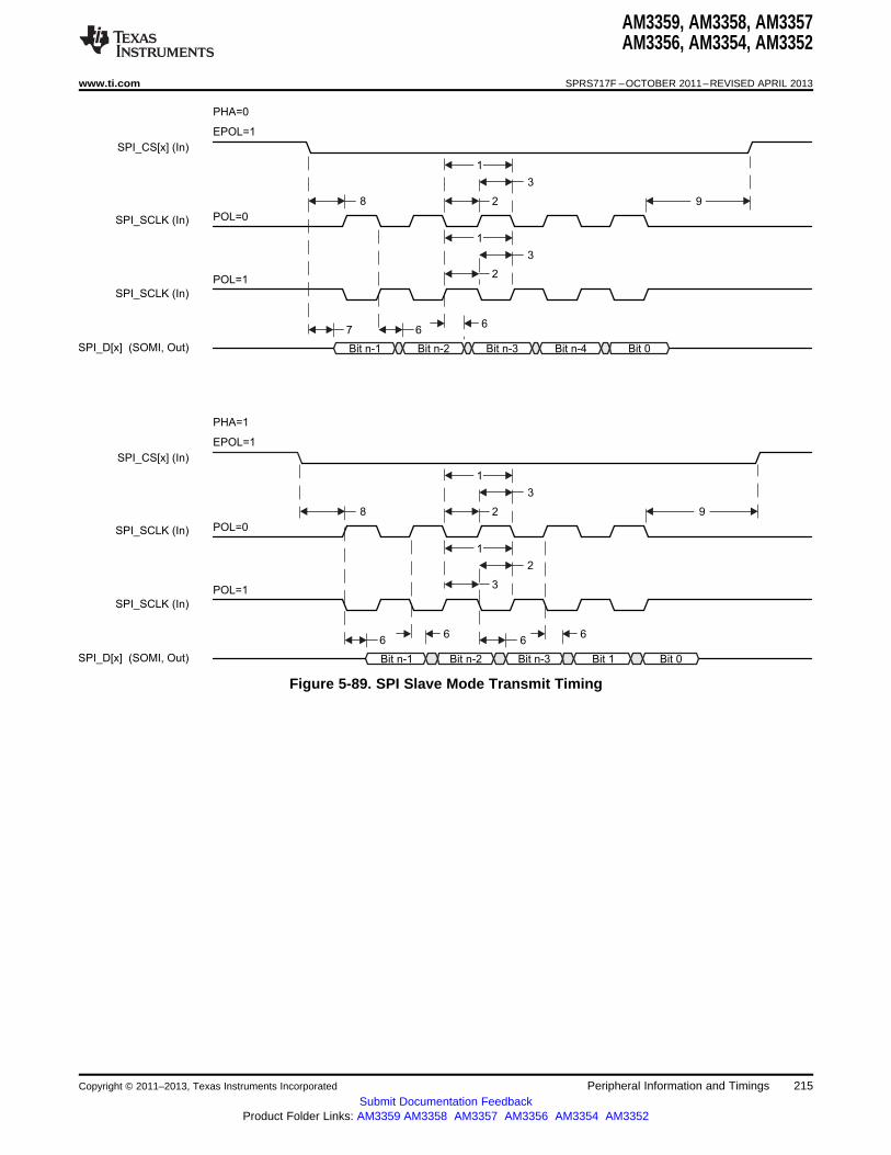
SPI_CS[x] (In)
SPI_SCLK (In)
SPI_SCLK (In)
SPI_D[x] (SOMI, Out) Bit n-1 Bit n-2 Bit n-3 Bit n-4 Bit 0
PHA=0
EPOL=1
POL=0
POL=1
8
3
76
2
1
2
1
SPI_CS[x] (In)
SPI_SCLK (In)
SPI_SCLK (In)
SPI_D[x] (SOMI, Out) Bit n-1 Bit n-2 Bit n-3 Bit 1 Bit 0
PHA=1
EPOL=1
POL=0
POL=1
8
3
6 6
2
1
2
3
1
6 6
9
6
9
3
AM3359, AM3358, AM3357AM3356, AM3354, AM3352
www.ti.com SPRS717F –OCTOBER 2011–REVISED APRIL 2013
Figure 5-89. SPI Slave Mode Transmit Timing
Copyright © 2011–2013, Texas Instruments Incorporated Peripheral Information and Timings 215Submit Documentation Feedback
Product Folder Links: AM3359 AM3358 AM3357 AM3356 AM3354 AM3352
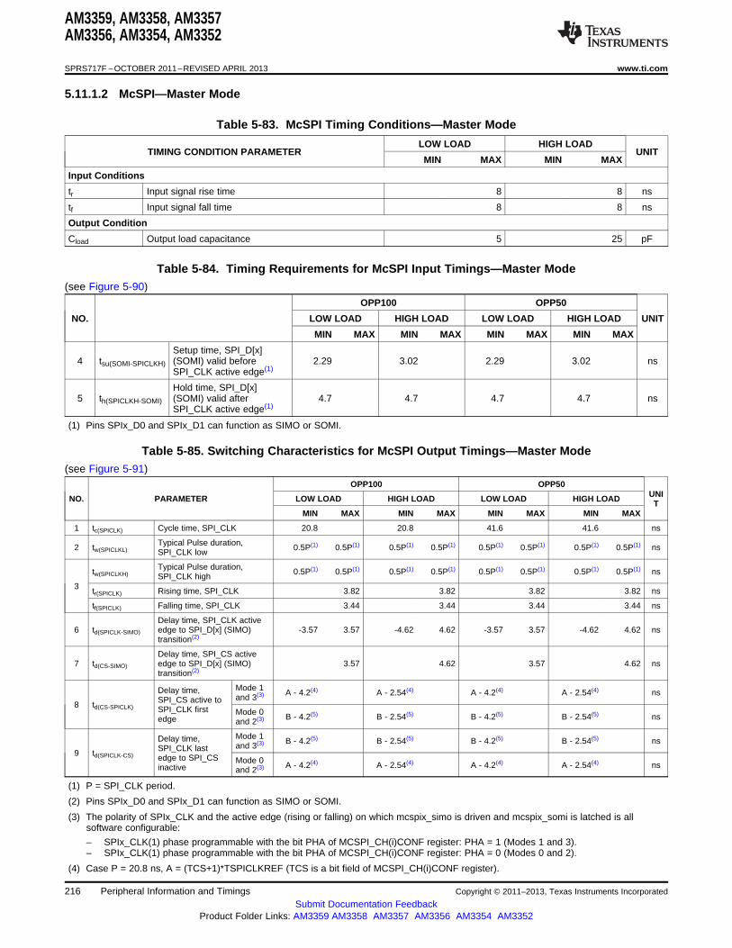
AM3359, AM3358, AM3357AM3356, AM3354, AM3352
SPRS717F –OCTOBER 2011–REVISED APRIL 2013 www.ti.com
5.11.1.2 McSPI—Master Mode
Table 5-83. McSPI Timing Conditions—Master Mode
LOW LOAD HIGH LOADTIMING CONDITION PARAMETER UNIT
MIN MAX MIN MAX
Input Conditions
tr Input signal rise time 8 8 ns
tf Input signal fall time 8 8 ns
Output Condition
Cload Output load capacitance 5 25 pF
Table 5-84. Timing Requirements for McSPI Input Timings—Master Mode(see Figure 5-90)
OPP100 OPP50
NO. LOW LOAD HIGH LOAD LOW LOAD HIGH LOAD UNIT
MIN MAX MIN MAX MIN MAX MIN MAX
Setup time, SPI_D[x]4 tsu(SOMI-SPICLKH) (SOMI) valid before 2.29 3.02 2.29 3.02 ns
SPI_CLK active edge(1)
Hold time, SPI_D[x]5 th(SPICLKH-SOMI) (SOMI) valid after 4.7 4.7 4.7 4.7 ns
SPI_CLK active edge(1)
(1) Pins SPIx_D0 and SPIx_D1 can function as SIMO or SOMI.
Table 5-85. Switching Characteristics for McSPI Output Timings—Master Mode(see Figure 5-91)
OPP100 OPP50UNINO. PARAMETER LOW LOAD HIGH LOAD LOW LOAD HIGH LOAD T
MIN MAX MIN MAX MIN MAX MIN MAX
1 tc(SPICLK) Cycle time, SPI_CLK 20.8 20.8 41.6 41.6 ns
Typical Pulse duration,2 tw(SPICLKL) 0.5P(1) 0.5P(1) 0.5P(1) 0.5P(1) 0.5P(1) 0.5P(1) 0.5P(1) 0.5P(1) nsSPI_CLK low
Typical Pulse duration,tw(SPICLKH) 0.5P(1) 0.5P(1) 0.5P(1) 0.5P(1) 0.5P(1) 0.5P(1) 0.5P(1) 0.5P(1) nsSPI_CLK high3 tr(SPICLK) Rising time, SPI_CLK 3.82 3.82 3.82 3.82 ns
tf(SPICLK) Falling time, SPI_CLK 3.44 3.44 3.44 3.44 ns
Delay time, SPI_CLK active6 td(SPICLK-SIMO) edge to SPI_D[x] (SIMO) -3.57 3.57 -4.62 4.62 -3.57 3.57 -4.62 4.62 ns
transition(2)
Delay time, SPI_CS active7 td(CS-SIMO) edge to SPI_D[x] (SIMO) 3.57 4.62 3.57 4.62 ns
transition(2)
Mode 1Delay time, A - 4.2(4) A - 2.54(4) A - 4.2(4) A - 2.54(4) nsand 3(3)SPI_CS active to8 td(CS-SPICLK) SPI_CLK first Mode 0 B - 4.2(5) B - 2.54(5) B - 4.2(5) B - 2.54(5) nsedge and 2(3)
Mode 1Delay time, B - 4.2(5) B - 2.54(5) B - 4.2(5) B - 2.54(5) nsand 3(3)SPI_CLK last9 td(SPICLK-CS) edge to SPI_CS Mode 0 A - 4.2(4) A - 2.54(4) A - 4.2(4) A - 2.54(4) nsinactive and 2(3)
(1) P = SPI_CLK period.
(2) Pins SPIx_D0 and SPIx_D1 can function as SIMO or SOMI.
(3) The polarity of SPIx_CLK and the active edge (rising or falling) on which mcspix_simo is driven and mcspix_somi is latched is allsoftware configurable:
– SPIx_CLK(1) phase programmable with the bit PHA of MCSPI_CH(i)CONF register: PHA = 1 (Modes 1 and 3).– SPIx_CLK(1) phase programmable with the bit PHA of MCSPI_CH(i)CONF register: PHA = 0 (Modes 0 and 2).
(4) Case P = 20.8 ns, A = (TCS+1)*TSPICLKREF (TCS is a bit field of MCSPI_CH(i)CONF register).
216 Peripheral Information and Timings Copyright © 2011–2013, Texas Instruments Incorporated
Submit Documentation FeedbackProduct Folder Links: AM3359 AM3358 AM3357 AM3356 AM3354 AM3352

SPI_CS[x] (Out)
SPI_SCLK (Out)
SPI_SCLK (Out)
SPI_D[x] (SOMI, In) Bit n-1 Bit n-2 Bit n-3 Bit n-4 Bit 0
PHA=0
EPOL=1
POL=0
POL=1
8 9
3
4
2
1
2
3
5
SPI_CS[x] (Out)
SPI_SCLK (Out)
SPI_SCLK (Out)
SPI_D[x] (SOMI, In) Bit n-1 Bit n-2 Bit n-3 Bit 1 Bit 0
PHA=1
EPOL=1
POL=0
POL=1
8 9
3
2
1
2
3
1
4
5
4
5 5
4
1
AM3359, AM3358, AM3357AM3356, AM3354, AM3352
www.ti.com SPRS717F –OCTOBER 2011–REVISED APRIL 2013
Case P > 20.8 ns, A = (TCS+0.5)*Fratio*TSPICLKREF (TCS is a bit field of MCSPI_CH(i)CONF register).Note: P = SPI_CLK clock period.
(5) B = (TCS+0.5)*TSPICLKREF*Fratio (TCS is a bit field of MCSPI_CH(i)CONF register, Fratio: Even≥2).
Figure 5-90. SPI Master Mode Receive Timing
Copyright © 2011–2013, Texas Instruments Incorporated Peripheral Information and Timings 217Submit Documentation Feedback
Product Folder Links: AM3359 AM3358 AM3357 AM3356 AM3354 AM3352
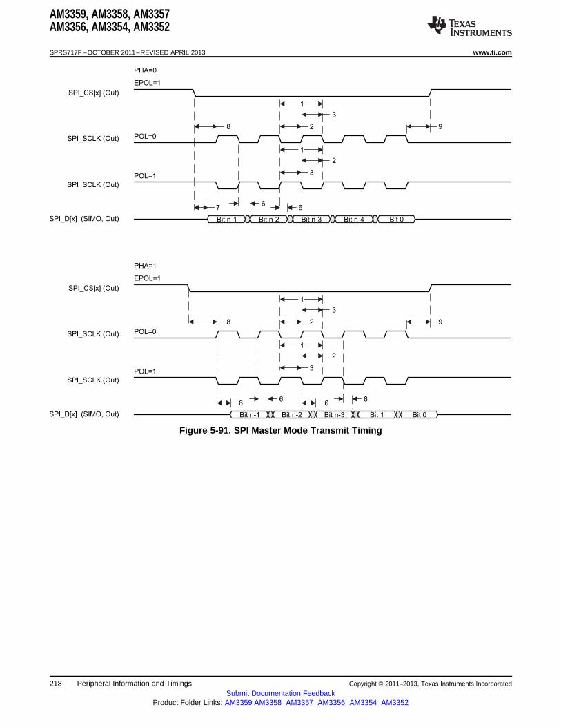
SPI_CS[x] (Out)
SPI_SCLK (Out)
SPI_SCLK (Out)
SPI_D[x] (SIMO, Out) Bit n-1 Bit n-2 Bit n-3 Bit n-4 Bit 0
PHA=0
EPOL=1
POL=0
POL=1
8 9
3
7 6
2
1
2
3
1
6
SPI_CS[x] (Out)
SPI_SCLK (Out)
SPI_SCLK (Out)
SPI_D[x] (SIMO, Out) Bit n-1 Bit n-2 Bit n-3 Bit 1 Bit 0
PHA=1
EPOL=1
POL=0
POL=1
8 9
3
6 6
2
1
2
3
1
6 6
AM3359, AM3358, AM3357AM3356, AM3354, AM3352
SPRS717F –OCTOBER 2011–REVISED APRIL 2013 www.ti.com
Figure 5-91. SPI Master Mode Transmit Timing
218 Peripheral Information and Timings Copyright © 2011–2013, Texas Instruments Incorporated
Submit Documentation FeedbackProduct Folder Links: AM3359 AM3358 AM3357 AM3356 AM3354 AM3352
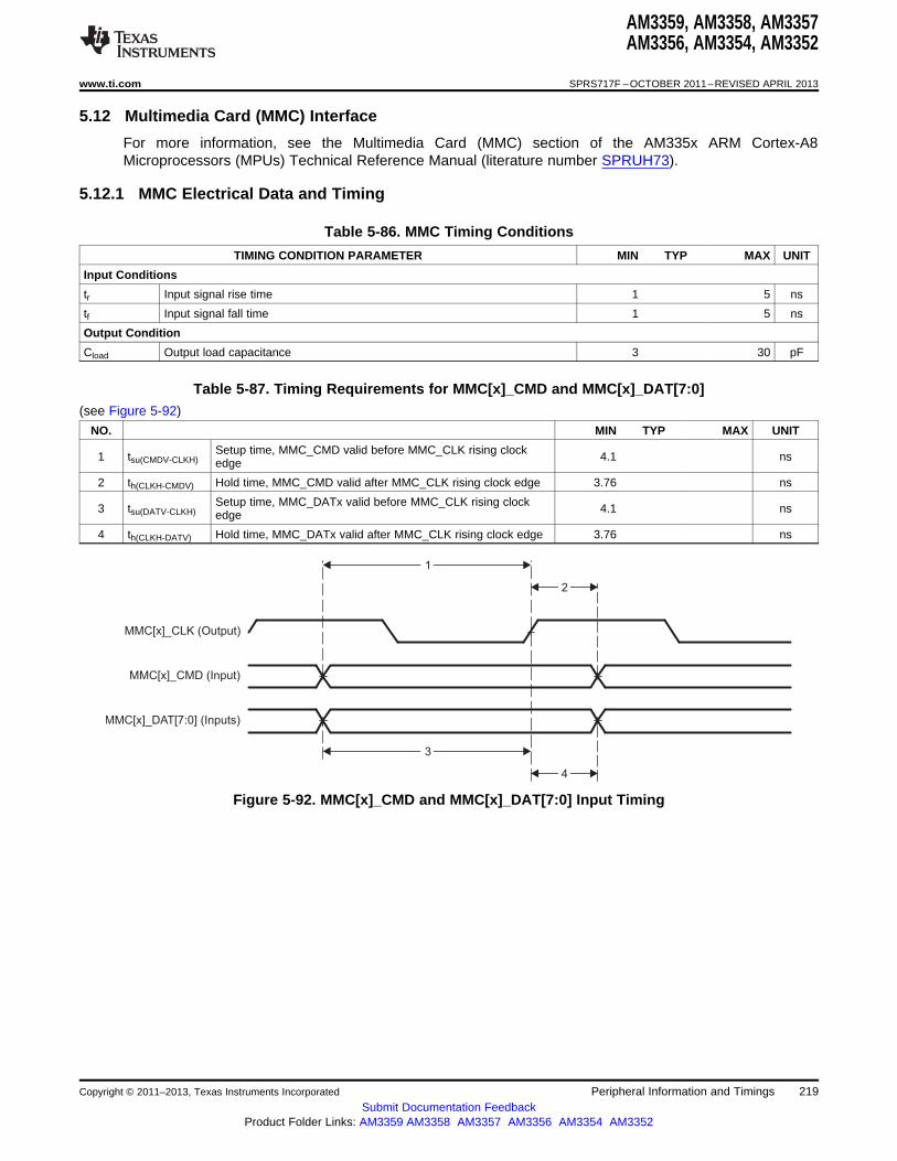
MMC[x]_CLK (Output)
1
2
MMC[x]_CMD (Input)
MMC[x]_DAT[7:0] (Inputs)
3
4
AM3359, AM3358, AM3357AM3356, AM3354, AM3352
www.ti.com SPRS717F –OCTOBER 2011–REVISED APRIL 2013
5.12 Multimedia Card (MMC) Interface
For more information, see the Multimedia Card (MMC) section of the AM335x ARM Cortex-A8Microprocessors (MPUs) Technical Reference Manual (literature number SPRUH73).
5.12.1 MMC Electrical Data and Timing
Table 5-86. MMC Timing Conditions
TIMING CONDITION PARAMETER MIN TYP MAX UNIT
Input Conditions
tr Input signal rise time 1 5 ns
tf Input signal fall time 1 5 ns
Output Condition
Cload Output load capacitance 3 30 pF
Table 5-87. Timing Requirements for MMC[x]_CMD and MMC[x]_DAT[7:0](see Figure 5-92)
NO. MIN TYP MAX UNIT
Setup time, MMC_CMD valid before MMC_CLK rising clock1 tsu(CMDV-CLKH) 4.1 nsedge
2 th(CLKH-CMDV) Hold time, MMC_CMD valid after MMC_CLK rising clock edge 3.76 ns
Setup time, MMC_DATx valid before MMC_CLK rising clock3 tsu(DATV-CLKH) 4.1 nsedge
4 th(CLKH-DATV) Hold time, MMC_DATx valid after MMC_CLK rising clock edge 3.76 ns
Figure 5-92. MMC[x]_CMD and MMC[x]_DAT[7:0] Input Timing
Copyright © 2011–2013, Texas Instruments Incorporated Peripheral Information and Timings 219Submit Documentation Feedback
Product Folder Links: AM3359 AM3358 AM3357 AM3356 AM3354 AM3352
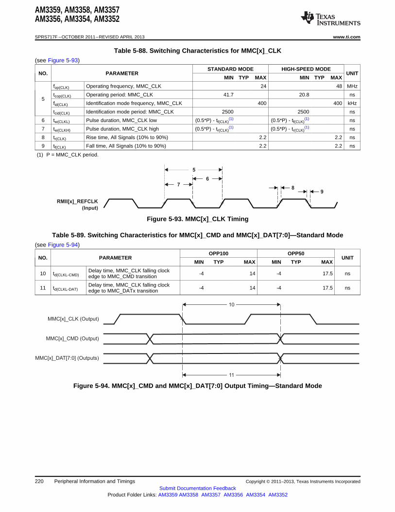
10
MMC[x]_CLK (Output)
MMC[x]_CMD (Output)
MMC[x]_DAT[7:0] (Outputs)
11
RMII[x]_REFCLK
(Input)
5
76
89
AM3359, AM3358, AM3357AM3356, AM3354, AM3352
SPRS717F –OCTOBER 2011–REVISED APRIL 2013 www.ti.com
Table 5-88. Switching Characteristics for MMC[x]_CLK(see Figure 5-93)
STANDARD MODE HIGH-SPEED MODENO. PARAMETER UNIT
MIN TYP MAX MIN TYP MAX
fop(CLK) Operating frequency, MMC_CLK 24 48 MHz
tcop(CLK) Operating period: MMC_CLK 41.7 20.8 ns5
fid(CLK) Identification mode frequency, MMC_CLK 400 400 kHz
tcid(CLK) Identification mode period: MMC_CLK 2500 2500 ns
6 tw(CLKL) Pulse duration, MMC_CLK low (0.5*P) - tf(CLK)(1) (0.5*P) - tf(CLK)
(1) ns
7 tw(CLKH) Pulse duration, MMC_CLK high (0.5*P) - tr(CLK)(1) (0.5*P) - tr(CLK)
(1) ns
8 tr(CLK) Rise time, All Signals (10% to 90%) 2.2 2.2 ns
9 tf(CLK) Fall time, All Signals (10% to 90%) 2.2 2.2 ns
(1) P = MMC_CLK period.
Figure 5-93. MMC[x]_CLK Timing
Table 5-89. Switching Characteristics for MMC[x]_CMD and MMC[x]_DAT[7:0]—Standard Mode(see Figure 5-94)
OPP100 OPP50NO. PARAMETER UNIT
MIN TYP MAX MIN TYP MAX
Delay time, MMC_CLK falling clock10 td(CLKL-CMD) -4 14 -4 17.5 nsedge to MMC_CMD transition
Delay time, MMC_CLK falling clock11 td(CLKL-DAT) -4 14 -4 17.5 nsedge to MMC_DATx transition
Figure 5-94. MMC[x]_CMD and MMC[x]_DAT[7:0] Output Timing—Standard Mode
220 Peripheral Information and Timings Copyright © 2011–2013, Texas Instruments Incorporated
Submit Documentation FeedbackProduct Folder Links: AM3359 AM3358 AM3357 AM3356 AM3354 AM3352
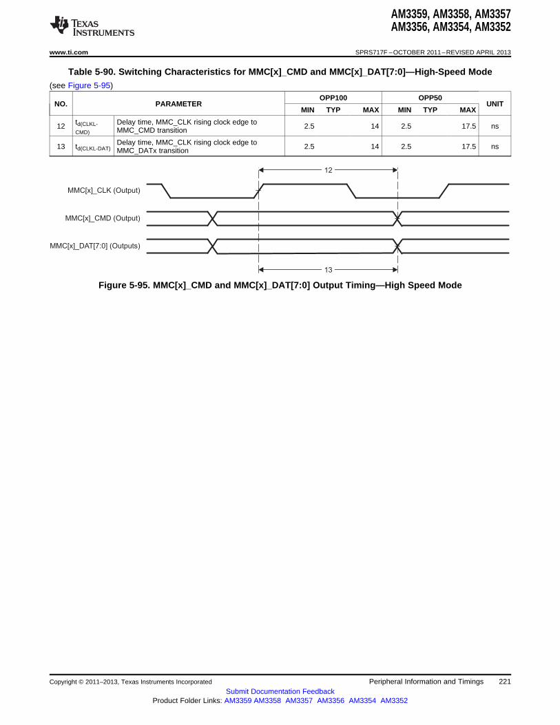
12
MMC[x]_CLK (Output)
MMC[x]_CMD (Output)
MMC[x]_DAT[7:0] (Outputs)
13
AM3359, AM3358, AM3357AM3356, AM3354, AM3352
www.ti.com SPRS717F –OCTOBER 2011–REVISED APRIL 2013
Table 5-90. Switching Characteristics for MMC[x]_CMD and MMC[x]_DAT[7:0]—High-Speed Mode(see Figure 5-95)
OPP100 OPP50NO. PARAMETER UNIT
MIN TYP MAX MIN TYP MAX
td(CLKL- Delay time, MMC_CLK rising clock edge to12 2.5 14 2.5 17.5 nsCMD) MMC_CMD transition
Delay time, MMC_CLK rising clock edge to13 td(CLKL-DAT) 2.5 14 2.5 17.5 nsMMC_DATx transition
Figure 5-95. MMC[x]_CMD and MMC[x]_DAT[7:0] Output Timing—High Speed Mode
Copyright © 2011–2013, Texas Instruments Incorporated Peripheral Information and Timings 221Submit Documentation Feedback
Product Folder Links: AM3359 AM3358 AM3357 AM3356 AM3354 AM3352

2
2
Start
Bit
Data Bits
UARTx_TXD
3
Data Bits
Bit
Start
3
UARTx_RXD
2
3
Stop Bit
Stop Bit
AM3359, AM3358, AM3357AM3356, AM3354, AM3352
SPRS717F –OCTOBER 2011–REVISED APRIL 2013 www.ti.com
5.13 Universal Asynchronous Receiver Transmitter (UART)
For more information, see the Universal Asynchronous Receiver Transmitter (UART) section of theAM335x ARM Cortex-A8 Microprocessors (MPUs) Technical Reference Manual (literature numberSPRUH73).
5.13.1 UART Electrical Data and Timing
Table 5-91. Timing Requirements for UARTx Receive(see Figure 5-96)
NO. MIN MAX UNIT
3 tw(RX) Pulse width, receive start, stop, data bit 0.96U(1) 1.05U(1) ns
(1) U = UART baud time = 1/programmed baud rate.
Table 5-92. Switching Characteristics for UARTx Transmit(see Figure 5-96)
NO. PARAMETER MIN MAX UNIT
1 fbaud(baud) Maximum programmable baud rate 3.6864 MHz
2 tw(TX) Pulse width, transmit start, stop, data bit U - 2(1) U + 2(1) ns
(1) U = UART baud time = 1/programmed baud rate.
Figure 5-96. UART Timings
222 Peripheral Information and Timings Copyright © 2011–2013, Texas Instruments Incorporated
Submit Documentation FeedbackProduct Folder Links: AM3359 AM3358 AM3357 AM3356 AM3354 AM3352

Pulse Duration
50%50% 50%
Pulse Duration
AM3359, AM3358, AM3357AM3356, AM3354, AM3352
www.ti.com SPRS717F –OCTOBER 2011–REVISED APRIL 2013
5.13.2 UART IrDA Interface
The IrDA module operates in three different modes:• Slow infrared (SIR) (≤ 115.2 Kbps)• Medium infrared (MIR) (0.576 Mbps and 1.152 Mbps)• Fast infrared (FIR) (4 Mbps).
Figure 5-97 illustrates the UART IrDA pulse parameters. Table 5-93 and Table 5-94 list the signaling ratesand pulse durations for UART IrDA receive and transmit modes.
Figure 5-97. UART IrDA Pulse Parameters
Table 5-93. UART IrDA—Signaling Rate and Pulse Duration—Receive Mode
ELECTRICAL PULSE DURATIONSIGNALING RATE UNIT
MIN MAX
SIR
2.4 Kbps 1.41 88.55 µs
9.6 Kbps 1.41 22.13 µs
19.2 Kbps 1.41 11.07 µs
38.4 Kbps 1.41 5.96 µs
57.6 Kbps 1.41 4.34 µs
115.2 Kbps 1.41 2.23 µs
MIR
0.576 Mbps 297.2 518.8 ns
1.152 Mbps 149.6 258.4 ns
FIR
4 Mbps (Single pulse) 67 164 ns
4 Mbps (Double pulse) 190 289 ns
Copyright © 2011–2013, Texas Instruments Incorporated Peripheral Information and Timings 223Submit Documentation Feedback
Product Folder Links: AM3359 AM3358 AM3357 AM3356 AM3354 AM3352
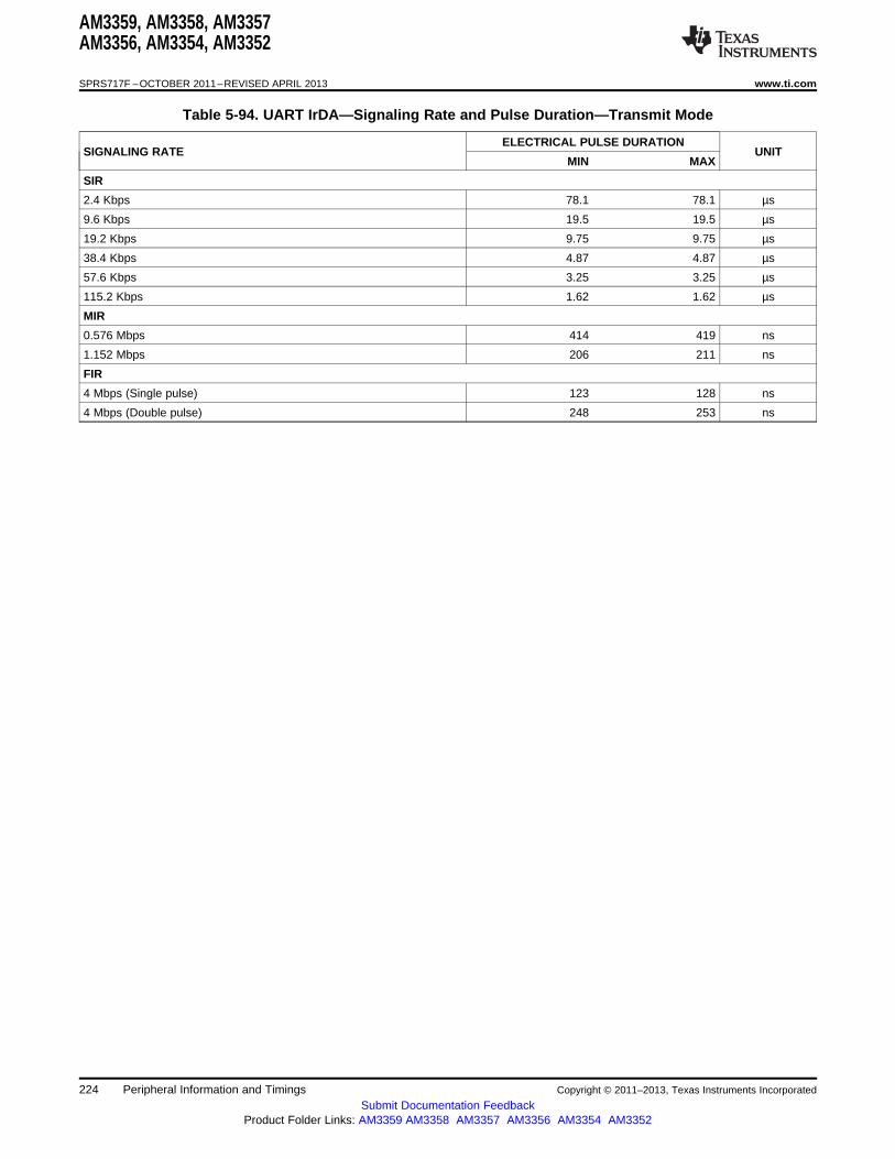
AM3359, AM3358, AM3357AM3356, AM3354, AM3352
SPRS717F –OCTOBER 2011–REVISED APRIL 2013 www.ti.com
Table 5-94. UART IrDA—Signaling Rate and Pulse Duration—Transmit Mode
ELECTRICAL PULSE DURATIONSIGNALING RATE UNIT
MIN MAX
SIR
2.4 Kbps 78.1 78.1 µs
9.6 Kbps 19.5 19.5 µs
19.2 Kbps 9.75 9.75 µs
38.4 Kbps 4.87 4.87 µs
57.6 Kbps 3.25 3.25 µs
115.2 Kbps 1.62 1.62 µs
MIR
0.576 Mbps 414 419 ns
1.152 Mbps 206 211 ns
FIR
4 Mbps (Single pulse) 123 128 ns
4 Mbps (Double pulse) 248 253 ns
224 Peripheral Information and Timings Copyright © 2011–2013, Texas Instruments Incorporated
Submit Documentation FeedbackProduct Folder Links: AM3359 AM3358 AM3357 AM3356 AM3354 AM3352

AM3359, AM3358, AM3357AM3356, AM3354, AM3352
www.ti.com SPRS717F –OCTOBER 2011–REVISED APRIL 2013
6 Device and Documentation Support
6.1 Device Support
6.1.1 Development Support
TI offers an extensive line of development tools, including tools to evaluate the performance of theprocessors, generate code, develop algorithm implementations, and fully integrate and debug softwareand hardware modules. The tool's support documentation is electronically available within the CodeComposer Studio™ Integrated Development Environment (IDE).
The following products support development of AM335x device applications:
Software Development Tools: Code Composer Studio™ Integrated Development Environment (IDE):including Editor C/C++/Assembly Code Generation, and Debug plus additional development toolsScalable, Real-Time Foundation Software (DSP/BIOS™), which provides the basic run-time targetsoftware needed to support any AM335x device application. DSP/BIOS™
Hardware Development Tools: Extended Development System (XDS™) Emulator XDS™
For a complete listing of development-support tools for the AM335x microprocessor platform, visit theTexas Instruments website at www.ti.com. For information on pricing and availability, contact the nearestTI field sales office or authorized distributor.
6.1.2 Device Nomenclature
To designate the stages in the product development cycle, TI assigns prefixes to the part numbers of allmicroprocessors (MPUs) and support tools. Each device has one of three prefixes: X, P, or null (no prefix)(for example, XAM3358AZCE). Texas Instruments recommends two of three possible prefix designatorsfor its support tools: TMDX and TMDS. These prefixes represent evolutionary stages of productdevelopment from engineering prototypes (TMDX) through fully qualified production devices and tools(TMDS).
Device development evolutionary flow:
X Experimental device that is not necessarily representative of the final device's electricalspecifications and may not use production assembly flow.
P Prototype device that is not necessarily the final silicon die and may not necessarily meetfinal electrical specifications.
null Production version of the silicon die that is fully qualified.
Support tool development evolutionary flow:
TMDX Development-support product that has not yet completed Texas Instruments internalqualification testing.
TMDS Fully-qualified development-support product.
X and P devices and TMDX development-support tools are shipped against the following disclaimer:
"Developmental product is intended for internal evaluation purposes."
Production devices and TMDS development-support tools have been characterized fully, and the qualityand reliability of the device have been demonstrated fully. TI's standard warranty applies.
Predictions show that prototype devices (X or P) have a greater failure rate than the standard productiondevices. Texas Instruments recommends that these devices not be used in any production systembecause their expected end-use failure rate still is undefined. Only qualified production devices are to beused.
Copyright © 2011–2013, Texas Instruments Incorporated Device and Documentation Support 225Submit Documentation Feedback
Product Folder Links: AM3359 AM3358 AM3357 AM3356 AM3354 AM3352
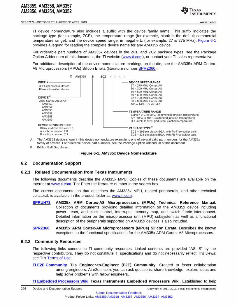
ARM Cortex-A8 MPU:AM3352
AM3358AM3359
AM3354AM3356AM3357
DEVICE(A)
PREFIX
AM3358
X = Experimental deviceBlank = Qualified device
ZCZ
PACKAGE TYPE(B)
ZCE = 298-pin plastic BGA, with Pb-Free solder ballsZCZ = 324-pin plastic BGA, with Pb-Free solder balls
DEVICE SPEED RANGE27 = 275-MHz Cortex-A830 = 300-MHz Cortex-A850 =
= 600-MHz= 720-MHz
500-MHz Cortex-A8Cortex-A8
72 Cortex-A880 = 800-MHz Cortex-A8100 = 1-GHz Cortex-A8
60
( )
TEMPERATURE RANGEBlank = 0°C to 90°C (commercial junction temperature)A = -40 extended junction temperature)D = -40 industrial junction temperature)
°C to 105°C (°C to 90°C (
( )B
DEVICE REVISION CODEBlank = silicon revision 1.0A = silicon revision 2.0B = silicon revision 2.1
X
AM3359, AM3358, AM3357AM3356, AM3354, AM3352
SPRS717F –OCTOBER 2011–REVISED APRIL 2013 www.ti.com
TI device nomenclature also includes a suffix with the device family name. This suffix indicates thepackage type (for example, ZCE), the temperature range (for example, blank is the default commercialtemperature range), and the device speed range, in megahertz (for example, 27 is 275 MHz). Figure 6-1provides a legend for reading the complete device name for any AM335x device.
For orderable part numbers of AM335x devices in the ZCE and ZCZ package types, see the PackageOption Addendum of this document, the TI website (www.ti.com), or contact your TI sales representative.
For additional description of the device nomenclature markings on the die, see the AM335x ARM Cortex-A8 Microprocessors (MPUs) Silicon Errata (literature number SPRZ360).
A. The AM3358 device shown in this device nomenclature example is one of several valid part numbers for the AM335xfamily of devices. For orderable device part numbers, see the Package Option Addendum of this document.
B. BGA = Ball Grid Array.
Figure 6-1. AM335x Device Nomenclature
6.2 Documentation Support
6.2.1 Related Documentation from Texas Instruments
The following documents describe the AM335x MPU. Copies of these documents are available on theInternet at www.ti.com. Tip: Enter the literature number in the search box.
The current documentation that describes the AM335x MPU, related peripherals, and other technicalcollateral, is available in the product folder at: www.ti.com.
SPRUH73 AM335x ARM Cortex-A8 Microprocessors (MPUs) Technical Reference Manual.Collection of documents providing detailed information on the AM335x device includingpower, reset, and clock control, interrupts, memory map, and switch fabric interconnect.Detailed information on the microprocessor unit (MPU) subsystem as well as a functionaldescription of the peripherals supported on AM335x devices is also included.
SPRZ360 AM335x ARM Cortex-A8 Microprocessors (MPUs) Silicon Errata. Describes the knownexceptions to the functional specifications for the AM335x ARM Cortex-A8 Microprocessors.
6.2.2 Community Resources
The following links connect to TI community resources. Linked contents are provided "AS IS" by therespective contributors. They do not constitute TI specifications and do not necessarily reflect TI's views;see TI's Terms of Use.
TI E2E Community TI's Engineer-to-Engineer (E2E) Community. Created to foster collaborationamong engineers. At e2e.ti.com, you can ask questions, share knowledge, explore ideas andhelp solve problems with fellow engineers.
TI Embedded Processors Wiki Texas Instruments Embedded Processors Wiki. Established to help
226 Device and Documentation Support Copyright © 2011–2013, Texas Instruments Incorporated
Submit Documentation FeedbackProduct Folder Links: AM3359 AM3358 AM3357 AM3356 AM3354 AM3352

AM3359, AM3358, AM3357AM3356, AM3354, AM3352
www.ti.com SPRS717F –OCTOBER 2011–REVISED APRIL 2013
developers get started with Embedded Processors from Texas Instruments and to fosterinnovation and growth of general knowledge about the hardware and software surroundingthese devices.
6.2.3 Related Documentation from Other Sources
The following documents are related to the AM335x MPU. Copies of these documents can be obtaineddirectly from the internet or from your Texas Instruments representative.
Cortex-A8 Technical Reference Manual. This is the technical reference manual for the Cortex-A8processor. A copy of this document can be obtained via the internet at http://infocenter.arm.com. Todetermine the revision of the Cortex-A8 core used on your device, see the AM335x ARM Cortex-A8Microprocessors (MPUs) Silicon Errata (literature number SPRZ360).
ARM Core Cortex™-A8 (AT400/AT401) Errata Notice. Provides a list of advisories for the differentrevisions of the Cortex-A8 processor. Contact your TI representative for a copy of this document. Todetermine the revision of the Cortex-A8 core used on your device, see the AM335x ARM Cortex-A8Microprocessors (MPUs) Silicon Errata (literature number SPRZ360).
Copyright © 2011–2013, Texas Instruments Incorporated Device and Documentation Support 227Submit Documentation Feedback
Product Folder Links: AM3359 AM3358 AM3357 AM3356 AM3354 AM3352

AM3359, AM3358, AM3357AM3356, AM3354, AM3352
SPRS717F –OCTOBER 2011–REVISED APRIL 2013 www.ti.com
7 Mechanical Packaging and Orderable Information
7.1 Thermal Data for ZCE and ZCZ Packages
Failure to maintain a junction temperature within the range specified in Table 3-12 reduces operatinglifetime, reliability, and performance—and may cause irreversible damage to the system. Therefore, theproduct design cycle should include thermal analysis to verify the maximum operating junctiontemperature of the device. It is important this thermal analysis is performed using specific system usecases and conditions. TI provides an application report to aid users in overcoming some of the existingchallenges of producing a good thermal design. For more information, see AM335x ThermalConsiderations (literature number SPRABT1).
Table 7-1 provides thermal characteristics for the packages used on this device.
NOTETable 7-1 provides simulation data and may not represent actual use-case values.
Table 7-1. Thermal Resistance Characteristics (PBGA Package) [ZCE and ZCZ]
NAME DESCRIPTION AIR ZCE ZCZFLOW (1) (°C/W) (2) (°C/W) (2)
ΘJC Junction-to-case (1S0P) (3) NA 10.3 10.2
ΘJB Junction-to-board (2S2P) (3) NA 11.6 12.1
ΘJA Junction-to-free air (2S2P) (3) 0.0 24.7 24.2
1.0 20.5 20.1
2.0 19.7 19.3
3.0 19.2 18.8
ΨJT Junction-to-package top (2S2P) (3) 0.0 0.4 0.3
1.0 0.6 0.6
2.0 0.7 0.7
3.0 0.9 0.8
ΨJB Junction-to-board (2S2P) (3) 0.0 11.9 12.7
1.0 11.7 12.3
2.0 11.7 12.3
3.0 11.6 12.2
(1) m/s = meters per second.(2) °C/W = degress celsius per watt.(3) The board types are defined by JEDEC (reference JEDEC standard JESD51-9, Test Board for Area
Array Surface Mount Package Thermal Measurements).
7.2 Via Channel
The ZCE package has been specially engineered with Via Channel™ technology. This allows larger thannormal PCB via and trace sizes and reduced PCB signal layers to be used in a PCB design with the 0.65-mm pitch package, and substantially reduces PCB costs. It allows PCB routing in only two signal layers(four layers total) due to the increased layer efficiency of the Via Channel™ BGA technology.
Via Channel™ technology implemented on the ZCE package makes it possible to build an AM335x-basedproduct with a 4-layer PCB, but a 4-layer PCB may not meet system performance goals. Therefore,system performance using a 4-layer PCB design must be evaluated during product design.
7.3 Packaging Information
The following packaging information and addendum reflect the most current data available for thedesignated devices. This data is subject to change without notice and without revision of this document.
228 Mechanical Packaging and Orderable Information Copyright © 2011–2013, Texas Instruments Incorporated
Submit Documentation FeedbackProduct Folder Links: AM3359 AM3358 AM3357 AM3356 AM3354 AM3352

PACKAGE OPTION ADDENDUM
www.ti.com 6-Jun-2013
Addendum-Page 1
PACKAGING INFORMATION
Orderable Device Status(1)
Package Type PackageDrawing
Pins PackageQty
Eco Plan(2)
Lead/Ball Finish MSL Peak Temp(3)
Op Temp (°C) Device Marking(4/5)
Samples
AM3352BZCE30 ACTIVE NFBGA ZCE 298 160 Green (RoHS& no Sb/Br)
SNAGCU Level-3-260C-168 HR 0 to 90 AM3352BZCE30
AM3352BZCE60 ACTIVE NFBGA ZCE 298 160 Green (RoHS& no Sb/Br)
SNAGCU Level-3-260C-168 HR 0 to 90 AM3352BZCE60
AM3352BZCEA30 ACTIVE NFBGA ZCE 298 160 Green (RoHS& no Sb/Br)
SNAGCU Level-3-260C-168 HR -40 to 105 AM3352BZCEA30
AM3352BZCEA30R ACTIVE NFBGA ZCE 298 1 Green (RoHS& no Sb/Br)
SNAGCU Level-3-260C-168 HR -40 to 105 AM3352BZCEA30
AM3352BZCEA60 ACTIVE NFBGA ZCE 298 160 Green (RoHS& no Sb/Br)
SNAGCU Level-3-260C-168 HR -40 to 105 AM3352BZCEA60
AM3352BZCEA60R ACTIVE NFBGA ZCE 298 1 Green (RoHS& no Sb/Br)
SNAGCU Level-3-260C-168 HR -40 to 105 AM3352BZCEA60
AM3352BZCED30 ACTIVE NFBGA ZCE 298 160 Green (RoHS& no Sb/Br)
SNAGCU Level-3-260C-168 HR -40 to 90 AM3352BZCED30
AM3352BZCED60 ACTIVE NFBGA ZCE 298 160 Green (RoHS& no Sb/Br)
SNAGCU Level-3-260C-168 HR -40 to 90 AM3352BZCED60
AM3352BZCZ100 ACTIVE NFBGA ZCZ 324 1 Green (RoHS& no Sb/Br)
SNAGCU Level-3-260C-168 HR 0 to 90 AM3352BZCZ100
AM3352BZCZ30 ACTIVE NFBGA ZCZ 324 126 Green (RoHS& no Sb/Br)
SNAGCU Level-3-260C-168 HR 0 to 90 AM3352BZCZ30
AM3352BZCZ60 ACTIVE NFBGA ZCZ 324 1 Green (RoHS& no Sb/Br)
SNAGCU Level-3-260C-168 HR 0 to 90 AM3352BZCZ60
AM3352BZCZ80 ACTIVE NFBGA ZCZ 324 126 Green (RoHS& no Sb/Br)
SNAGCU Level-3-260C-168 HR 0 to 90 AM3352BZCZ80
AM3352BZCZA100 ACTIVE NFBGA ZCZ 324 126 Green (RoHS& no Sb/Br)
SNAGCU Level-3-260C-168 HR -40 to 105 AM3352BZCZA100
AM3352BZCZA30 ACTIVE NFBGA ZCZ 324 126 Green (RoHS& no Sb/Br)
SNAGCU Level-3-260C-168 HR -40 to 105 AM3352BZCZA30
AM3352BZCZA60 ACTIVE NFBGA ZCZ 324 126 Green (RoHS& no Sb/Br)
SNAGCU Level-3-260C-168 HR -40 to 105 AM3352BZCZA60
AM3352BZCZA80 ACTIVE NFBGA ZCZ 324 126 Green (RoHS& no Sb/Br)
SNAGCU Level-3-260C-168 HR -40 to 105 AM3352BZCZA80
AM3352BZCZD30 ACTIVE NFBGA ZCZ 324 126 Green (RoHS& no Sb/Br)
SNAGCU Level-3-260C-168 HR -40 to 90 AM3352BZCZD30
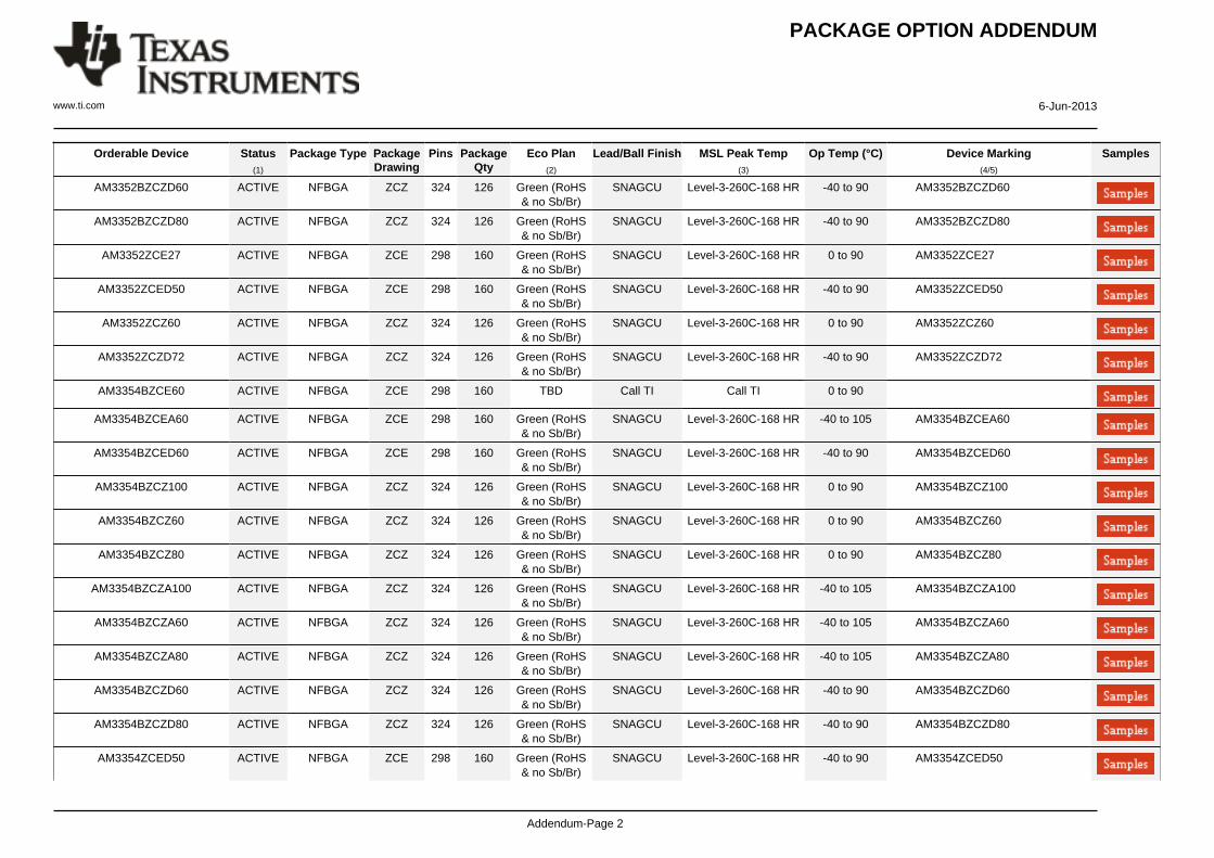
PACKAGE OPTION ADDENDUM
www.ti.com 6-Jun-2013
Addendum-Page 2
Orderable Device Status(1)
Package Type PackageDrawing
Pins PackageQty
Eco Plan(2)
Lead/Ball Finish MSL Peak Temp(3)
Op Temp (°C) Device Marking(4/5)
Samples
AM3352BZCZD60 ACTIVE NFBGA ZCZ 324 126 Green (RoHS& no Sb/Br)
SNAGCU Level-3-260C-168 HR -40 to 90 AM3352BZCZD60
AM3352BZCZD80 ACTIVE NFBGA ZCZ 324 126 Green (RoHS& no Sb/Br)
SNAGCU Level-3-260C-168 HR -40 to 90 AM3352BZCZD80
AM3352ZCE27 ACTIVE NFBGA ZCE 298 160 Green (RoHS& no Sb/Br)
SNAGCU Level-3-260C-168 HR 0 to 90 AM3352ZCE27
AM3352ZCED50 ACTIVE NFBGA ZCE 298 160 Green (RoHS& no Sb/Br)
SNAGCU Level-3-260C-168 HR -40 to 90 AM3352ZCED50
AM3352ZCZ60 ACTIVE NFBGA ZCZ 324 126 Green (RoHS& no Sb/Br)
SNAGCU Level-3-260C-168 HR 0 to 90 AM3352ZCZ60
AM3352ZCZD72 ACTIVE NFBGA ZCZ 324 126 Green (RoHS& no Sb/Br)
SNAGCU Level-3-260C-168 HR -40 to 90 AM3352ZCZD72
AM3354BZCE60 ACTIVE NFBGA ZCE 298 160 TBD Call TI Call TI 0 to 90
AM3354BZCEA60 ACTIVE NFBGA ZCE 298 160 Green (RoHS& no Sb/Br)
SNAGCU Level-3-260C-168 HR -40 to 105 AM3354BZCEA60
AM3354BZCED60 ACTIVE NFBGA ZCE 298 160 Green (RoHS& no Sb/Br)
SNAGCU Level-3-260C-168 HR -40 to 90 AM3354BZCED60
AM3354BZCZ100 ACTIVE NFBGA ZCZ 324 126 Green (RoHS& no Sb/Br)
SNAGCU Level-3-260C-168 HR 0 to 90 AM3354BZCZ100
AM3354BZCZ60 ACTIVE NFBGA ZCZ 324 126 Green (RoHS& no Sb/Br)
SNAGCU Level-3-260C-168 HR 0 to 90 AM3354BZCZ60
AM3354BZCZ80 ACTIVE NFBGA ZCZ 324 126 Green (RoHS& no Sb/Br)
SNAGCU Level-3-260C-168 HR 0 to 90 AM3354BZCZ80
AM3354BZCZA100 ACTIVE NFBGA ZCZ 324 126 Green (RoHS& no Sb/Br)
SNAGCU Level-3-260C-168 HR -40 to 105 AM3354BZCZA100
AM3354BZCZA60 ACTIVE NFBGA ZCZ 324 126 Green (RoHS& no Sb/Br)
SNAGCU Level-3-260C-168 HR -40 to 105 AM3354BZCZA60
AM3354BZCZA80 ACTIVE NFBGA ZCZ 324 126 Green (RoHS& no Sb/Br)
SNAGCU Level-3-260C-168 HR -40 to 105 AM3354BZCZA80
AM3354BZCZD60 ACTIVE NFBGA ZCZ 324 126 Green (RoHS& no Sb/Br)
SNAGCU Level-3-260C-168 HR -40 to 90 AM3354BZCZD60
AM3354BZCZD80 ACTIVE NFBGA ZCZ 324 126 Green (RoHS& no Sb/Br)
SNAGCU Level-3-260C-168 HR -40 to 90 AM3354BZCZD80
AM3354ZCED50 ACTIVE NFBGA ZCE 298 160 Green (RoHS& no Sb/Br)
SNAGCU Level-3-260C-168 HR -40 to 90 AM3354ZCED50
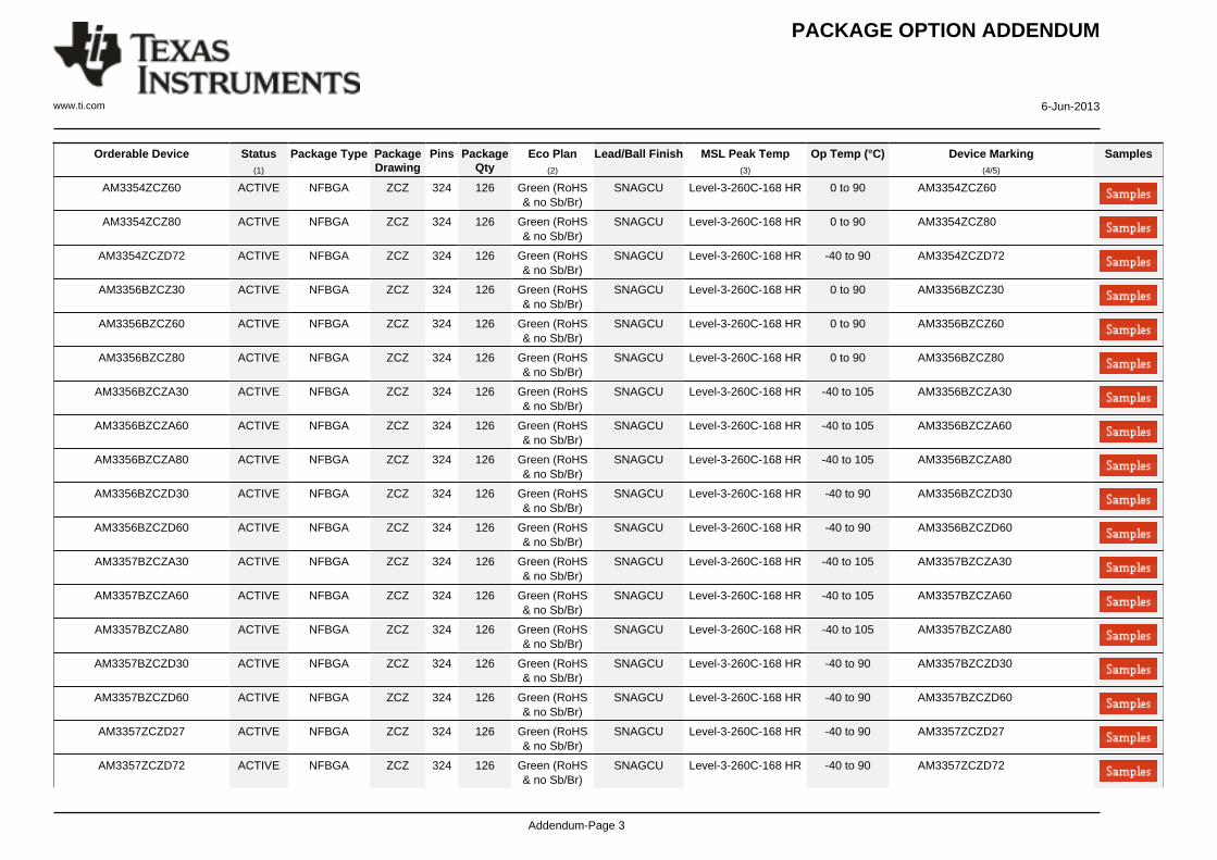
PACKAGE OPTION ADDENDUM
www.ti.com 6-Jun-2013
Addendum-Page 3
Orderable Device Status(1)
Package Type PackageDrawing
Pins PackageQty
Eco Plan(2)
Lead/Ball Finish MSL Peak Temp(3)
Op Temp (°C) Device Marking(4/5)
Samples
AM3354ZCZ60 ACTIVE NFBGA ZCZ 324 126 Green (RoHS& no Sb/Br)
SNAGCU Level-3-260C-168 HR 0 to 90 AM3354ZCZ60
AM3354ZCZ80 ACTIVE NFBGA ZCZ 324 126 Green (RoHS& no Sb/Br)
SNAGCU Level-3-260C-168 HR 0 to 90 AM3354ZCZ80
AM3354ZCZD72 ACTIVE NFBGA ZCZ 324 126 Green (RoHS& no Sb/Br)
SNAGCU Level-3-260C-168 HR -40 to 90 AM3354ZCZD72
AM3356BZCZ30 ACTIVE NFBGA ZCZ 324 126 Green (RoHS& no Sb/Br)
SNAGCU Level-3-260C-168 HR 0 to 90 AM3356BZCZ30
AM3356BZCZ60 ACTIVE NFBGA ZCZ 324 126 Green (RoHS& no Sb/Br)
SNAGCU Level-3-260C-168 HR 0 to 90 AM3356BZCZ60
AM3356BZCZ80 ACTIVE NFBGA ZCZ 324 126 Green (RoHS& no Sb/Br)
SNAGCU Level-3-260C-168 HR 0 to 90 AM3356BZCZ80
AM3356BZCZA30 ACTIVE NFBGA ZCZ 324 126 Green (RoHS& no Sb/Br)
SNAGCU Level-3-260C-168 HR -40 to 105 AM3356BZCZA30
AM3356BZCZA60 ACTIVE NFBGA ZCZ 324 126 Green (RoHS& no Sb/Br)
SNAGCU Level-3-260C-168 HR -40 to 105 AM3356BZCZA60
AM3356BZCZA80 ACTIVE NFBGA ZCZ 324 126 Green (RoHS& no Sb/Br)
SNAGCU Level-3-260C-168 HR -40 to 105 AM3356BZCZA80
AM3356BZCZD30 ACTIVE NFBGA ZCZ 324 126 Green (RoHS& no Sb/Br)
SNAGCU Level-3-260C-168 HR -40 to 90 AM3356BZCZD30
AM3356BZCZD60 ACTIVE NFBGA ZCZ 324 126 Green (RoHS& no Sb/Br)
SNAGCU Level-3-260C-168 HR -40 to 90 AM3356BZCZD60
AM3357BZCZA30 ACTIVE NFBGA ZCZ 324 126 Green (RoHS& no Sb/Br)
SNAGCU Level-3-260C-168 HR -40 to 105 AM3357BZCZA30
AM3357BZCZA60 ACTIVE NFBGA ZCZ 324 126 Green (RoHS& no Sb/Br)
SNAGCU Level-3-260C-168 HR -40 to 105 AM3357BZCZA60
AM3357BZCZA80 ACTIVE NFBGA ZCZ 324 126 Green (RoHS& no Sb/Br)
SNAGCU Level-3-260C-168 HR -40 to 105 AM3357BZCZA80
AM3357BZCZD30 ACTIVE NFBGA ZCZ 324 126 Green (RoHS& no Sb/Br)
SNAGCU Level-3-260C-168 HR -40 to 90 AM3357BZCZD30
AM3357BZCZD60 ACTIVE NFBGA ZCZ 324 126 Green (RoHS& no Sb/Br)
SNAGCU Level-3-260C-168 HR -40 to 90 AM3357BZCZD60
AM3357ZCZD27 ACTIVE NFBGA ZCZ 324 126 Green (RoHS& no Sb/Br)
SNAGCU Level-3-260C-168 HR -40 to 90 AM3357ZCZD27
AM3357ZCZD72 ACTIVE NFBGA ZCZ 324 126 Green (RoHS& no Sb/Br)
SNAGCU Level-3-260C-168 HR -40 to 90 AM3357ZCZD72
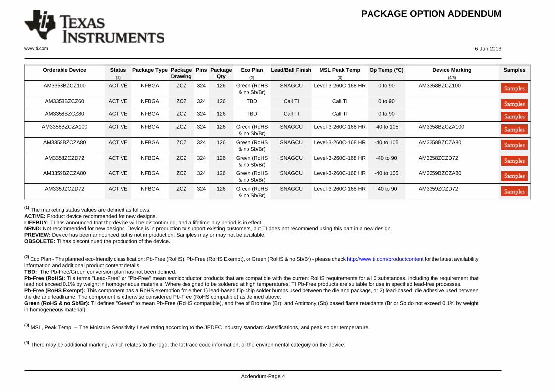
PACKAGE OPTION ADDENDUM
www.ti.com 6-Jun-2013
Addendum-Page 4
Orderable Device Status(1)
Package Type PackageDrawing
Pins PackageQty
Eco Plan(2)
Lead/Ball Finish MSL Peak Temp(3)
Op Temp (°C) Device Marking(4/5)
Samples
AM3358BZCZ100 ACTIVE NFBGA ZCZ 324 126 Green (RoHS& no Sb/Br)
SNAGCU Level-3-260C-168 HR 0 to 90 AM3358BZCZ100
AM3358BZCZ60 ACTIVE NFBGA ZCZ 324 126 TBD Call TI Call TI 0 to 90
AM3358BZCZ80 ACTIVE NFBGA ZCZ 324 126 TBD Call TI Call TI 0 to 90
AM3358BZCZA100 ACTIVE NFBGA ZCZ 324 126 Green (RoHS& no Sb/Br)
SNAGCU Level-3-260C-168 HR -40 to 105 AM3358BZCZA100
AM3358BZCZA80 ACTIVE NFBGA ZCZ 324 126 Green (RoHS& no Sb/Br)
SNAGCU Level-3-260C-168 HR -40 to 105 AM3358BZCZA80
AM3358ZCZD72 ACTIVE NFBGA ZCZ 324 126 Green (RoHS& no Sb/Br)
SNAGCU Level-3-260C-168 HR -40 to 90 AM3358ZCZD72
AM3359BZCZA80 ACTIVE NFBGA ZCZ 324 126 Green (RoHS& no Sb/Br)
SNAGCU Level-3-260C-168 HR -40 to 105 AM3359BZCZA80
AM3359ZCZD72 ACTIVE NFBGA ZCZ 324 126 Green (RoHS& no Sb/Br)
SNAGCU Level-3-260C-168 HR -40 to 90 AM3359ZCZD72
(1) The marketing status values are defined as follows:ACTIVE: Product device recommended for new designs.LIFEBUY: TI has announced that the device will be discontinued, and a lifetime-buy period is in effect.NRND: Not recommended for new designs. Device is in production to support existing customers, but TI does not recommend using this part in a new design.PREVIEW: Device has been announced but is not in production. Samples may or may not be available.OBSOLETE: TI has discontinued the production of the device.
(2) Eco Plan - The planned eco-friendly classification: Pb-Free (RoHS), Pb-Free (RoHS Exempt), or Green (RoHS & no Sb/Br) - please check http://www.ti.com/productcontent for the latest availabilityinformation and additional product content details.TBD: The Pb-Free/Green conversion plan has not been defined.Pb-Free (RoHS): TI's terms "Lead-Free" or "Pb-Free" mean semiconductor products that are compatible with the current RoHS requirements for all 6 substances, including the requirement thatlead not exceed 0.1% by weight in homogeneous materials. Where designed to be soldered at high temperatures, TI Pb-Free products are suitable for use in specified lead-free processes.Pb-Free (RoHS Exempt): This component has a RoHS exemption for either 1) lead-based flip-chip solder bumps used between the die and package, or 2) lead-based die adhesive used betweenthe die and leadframe. The component is otherwise considered Pb-Free (RoHS compatible) as defined above.Green (RoHS & no Sb/Br): TI defines "Green" to mean Pb-Free (RoHS compatible), and free of Bromine (Br) and Antimony (Sb) based flame retardants (Br or Sb do not exceed 0.1% by weightin homogeneous material)
(3) MSL, Peak Temp. -- The Moisture Sensitivity Level rating according to the JEDEC industry standard classifications, and peak solder temperature.
(4) There may be additional marking, which relates to the logo, the lot trace code information, or the environmental category on the device.
PACKAGE OPTION ADDENDUM
www.ti.com 6-Jun-2013
Addendum-Page 5
(5) Multiple Device Markings will be inside parentheses. Only one Device Marking contained in parentheses and separated by a "~" will appear on a device. If a line is indented then it is a continuationof the previous line and the two combined represent the entire Device Marking for that device.
Important Information and Disclaimer:The information provided on this page represents TI's knowledge and belief as of the date that it is provided. TI bases its knowledge and belief on informationprovided by third parties, and makes no representation or warranty as to the accuracy of such information. Efforts are underway to better integrate information from third parties. TI has taken andcontinues to take reasonable steps to provide representative and accurate information but may not have conducted destructive testing or chemical analysis on incoming materials and chemicals.TI and TI suppliers consider certain information to be proprietary, and thus CAS numbers and other limited information may not be available for release.
In no event shall TI's liability arising out of such information exceed the total purchase price of the TI part(s) at issue in this document sold by TI to Customer on an annual basis.
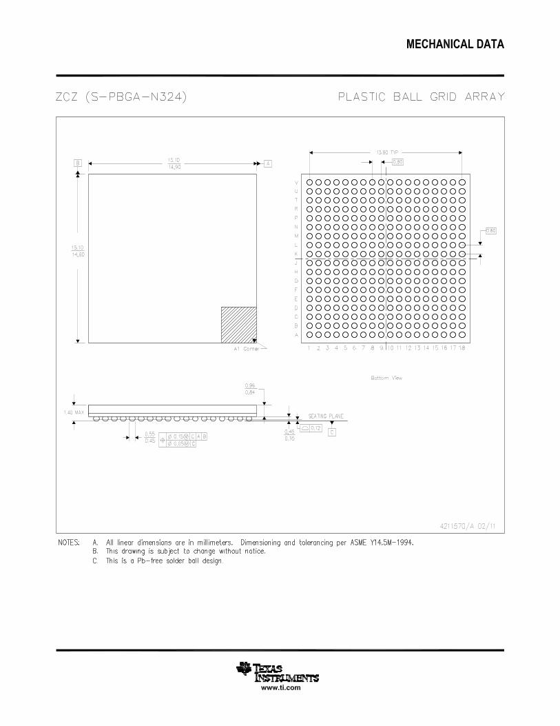
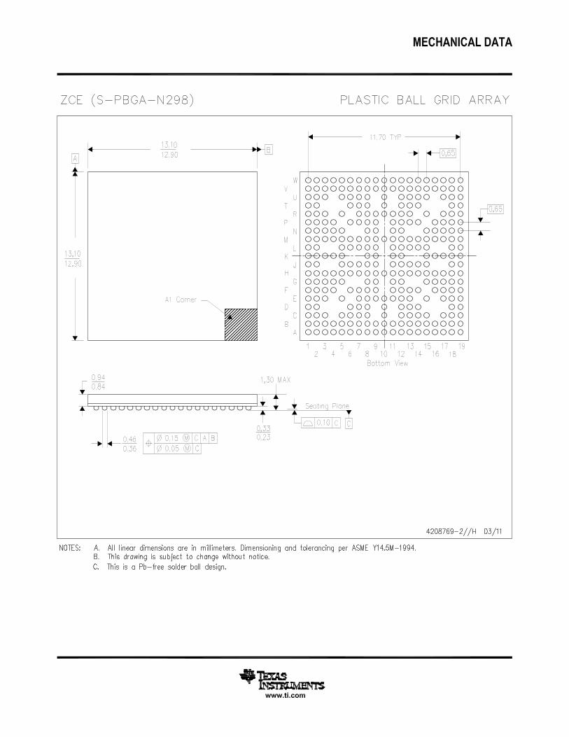

IMPORTANT NOTICE
Texas Instruments Incorporated and its subsidiaries (TI) reserve the right to make corrections, enhancements, improvements and otherchanges to its semiconductor products and services per JESD46, latest issue, and to discontinue any product or service per JESD48, latestissue. Buyers should obtain the latest relevant information before placing orders and should verify that such information is current andcomplete. All semiconductor products (also referred to herein as “components”) are sold subject to TI’s terms and conditions of salesupplied at the time of order acknowledgment.
TI warrants performance of its components to the specifications applicable at the time of sale, in accordance with the warranty in TI’s termsand conditions of sale of semiconductor products. Testing and other quality control techniques are used to the extent TI deems necessaryto support this warranty. Except where mandated by applicable law, testing of all parameters of each component is not necessarilyperformed.
TI assumes no liability for applications assistance or the design of Buyers’ products. Buyers are responsible for their products andapplications using TI components. To minimize the risks associated with Buyers’ products and applications, Buyers should provideadequate design and operating safeguards.
TI does not warrant or represent that any license, either express or implied, is granted under any patent right, copyright, mask work right, orother intellectual property right relating to any combination, machine, or process in which TI components or services are used. Informationpublished by TI regarding third-party products or services does not constitute a license to use such products or services or a warranty orendorsement thereof. Use of such information may require a license from a third party under the patents or other intellectual property of thethird party, or a license from TI under the patents or other intellectual property of TI.
Reproduction of significant portions of TI information in TI data books or data sheets is permissible only if reproduction is without alterationand is accompanied by all associated warranties, conditions, limitations, and notices. TI is not responsible or liable for such altereddocumentation. Information of third parties may be subject to additional restrictions.
Resale of TI components or services with statements different from or beyond the parameters stated by TI for that component or servicevoids all express and any implied warranties for the associated TI component or service and is an unfair and deceptive business practice.TI is not responsible or liable for any such statements.
Buyer acknowledges and agrees that it is solely responsible for compliance with all legal, regulatory and safety-related requirementsconcerning its products, and any use of TI components in its applications, notwithstanding any applications-related information or supportthat may be provided by TI. Buyer represents and agrees that it has all the necessary expertise to create and implement safeguards whichanticipate dangerous consequences of failures, monitor failures and their consequences, lessen the likelihood of failures that might causeharm and take appropriate remedial actions. Buyer will fully indemnify TI and its representatives against any damages arising out of the useof any TI components in safety-critical applications.
In some cases, TI components may be promoted specifically to facilitate safety-related applications. With such components, TI’s goal is tohelp enable customers to design and create their own end-product solutions that meet applicable functional safety standards andrequirements. Nonetheless, such components are subject to these terms.
No TI components are authorized for use in FDA Class III (or similar life-critical medical equipment) unless authorized officers of the partieshave executed a special agreement specifically governing such use.
Only those TI components which TI has specifically designated as military grade or “enhanced plastic” are designed and intended for use inmilitary/aerospace applications or environments. Buyer acknowledges and agrees that any military or aerospace use of TI componentswhich have not been so designated is solely at the Buyer's risk, and that Buyer is solely responsible for compliance with all legal andregulatory requirements in connection with such use.
TI has specifically designated certain components as meeting ISO/TS16949 requirements, mainly for automotive use. In any case of use ofnon-designated products, TI will not be responsible for any failure to meet ISO/TS16949.
Products Applications
Audio www.ti.com/audio Automotive and Transportation www.ti.com/automotive
Amplifiers amplifier.ti.com Communications and Telecom www.ti.com/communications
Data Converters dataconverter.ti.com Computers and Peripherals www.ti.com/computers
DLP® Products www.dlp.com Consumer Electronics www.ti.com/consumer-apps
DSP dsp.ti.com Energy and Lighting www.ti.com/energy
Clocks and Timers www.ti.com/clocks Industrial www.ti.com/industrial
Interface interface.ti.com Medical www.ti.com/medical
Logic logic.ti.com Security www.ti.com/security
Power Mgmt power.ti.com Space, Avionics and Defense www.ti.com/space-avionics-defense
Microcontrollers microcontroller.ti.com Video and Imaging www.ti.com/video
RFID www.ti-rfid.com
OMAP Applications Processors www.ti.com/omap TI E2E Community e2e.ti.com
Wireless Connectivity www.ti.com/wirelessconnectivity
Mailing Address: Texas Instruments, Post Office Box 655303, Dallas, Texas 75265Copyright © 2013, Texas Instruments Incorporated