Product Folder Sample & Buy Technical Documents Tools & Software Support & Community TMS320DM8168, TMS320DM8167 TMS320DM8165 SPRS614F – MARCH 2011 – REVISED MARCH 2015 TMS320DM816x DaVinci™ Digital Media Processors 1 Device Overview 1.1 Features 1 • High-Performance DaVinci Digital Media • System Memory Management Unit (System MMU) Processors – Maps C674x DSP and EMDA TCB Memory – ARM ® Cortex™-A8 RISC Processor Accesses to System Addresses • 512KB of On-Chip Memory Controller (OCMC) • Up to 1.20 GHz RAM – C674x™ VLIW DSP • Media Controller • Up to 1 GHz – Manages HDVPSS and HDVICP2 Modules • Up to 8000 MIPS and 6000 MFLOPS • Up to Three Programmable High-Definition Video • Fully Software-Compatible with C67x+ and Image Coprocessing (HDVICP2) Engines C64x+™ – Encode, Decode, Transcode Operations • ARM Cortex-A8 Core – H.264, MPEG-2, VC-1, MPEG-4 SP and ASP – ARMv7 Architecture • SGX530 3D Graphics Engine (Available Only on • In-Order, Dual-Issue, Superscalar Processor the DM8168 Device) Core – Delivers up to 30 MTriangles per Second • NEON™ Multimedia Architecture – Universal Scalable Shader Engine – Supports Integer and Floating Point (VFPv3- – Direct3D ® Mobile, OpenGL ® ES 1.1 and 2.0, IEEE754 Compliant) OpenVG™ 1.1, OpenMax™ API Support • Jazelle ® RCT Execution Environment – Advanced Geometry DMA Driven Operation • ARM Cortex-A8 Memory Architecture – Programmable HQ Image Anti-Aliasing – 32-KB Instruction and Data Caches • Endianness – 256-KB L2 Cache – ARM, DSP Instructions and Data – Little Endian – 64-KB RAM, 48-KB of Boot ROM • HD Video Processing Subsystem (HDVPSS) • TMS320C674x Floating-Point VLIW DSP – Two 165-MHz HD Video Capture Channels – 64 General-Purpose Registers (32-Bit) • One 16-Bit or 24-Bit and One 16-Bit Channel – Six ALU (32-Bit and 40-Bit) Functional Units • Each Channel Splittable Into Dual 8-Bit • Supports 32-Bit Integer, SP (IEEE Single Capture Channels Precision, 32-Bit) and DP (IEEE Double – Two 165-MHz HD Video Display Channels Precision, 64-Bit) Floating Point • One 16-Bit, 24-Bit, 30-Bit Channel and One • Supports up to Four SP Adds Per Clock and 16-Bit Channel Four DP Adds Every Two Clocks – Simultaneous SD and HD Analog Output • Supports up to Two Floating-Point (SP or DP) Approximate Reciprocal or Square Root – Digital HDMI 1.3 Transmitter with PHY with Operations Per Cycle HDCP up to 165-MHz Pixel Clock – Two Multiply Functional Units – Three Graphics Layers • Mixed-Precision IEEE Floating-Point Multiply • Dual 32-Bit DDR2 and DDR3 SDRAM Interfaces Supported up to: – Supports up to DDR2-800 and DDR3-1600 – 2 SP x SP → SP Per Clock – Up to Eight x8 Devices Total – 2 SP x SP → DP Every Two Clocks – 2GB of Total Address Space – 2 SP x DP → DP Every Three Clocks – Dynamic Memory Manager (DMM) – 2 DP x DP → DP Every Four Clocks • Programmable Multi-Zone Memory Mapping • Fixed-Point Multiply Supports Two 32 x 32 and Interleaving Multiplies, Four 16 x 16-Bit Multiplies • Enables Efficient 2D Block Accesses Including Complex Multiplies, or Eight 8 x 8- • Supports Tiled Objects in 0°, 90°, 180°, or Bit Multiplies per Clock Cycle 270° Orientation and Mirroring • C674x Two-Level Memory Architecture • Optimizes Interlaced Accesses – 32-KB L1P and L1D RAM and Cache • One PCI Express ® (PCIe) 2.0 Port with Integrated – 256-KB L2 Unified Mapped RAM and Caches PHY 1 An IMPORTANT NOTICE at the end of this data sheet addresses availability, warranty, changes, use in safety-critical applications, intellectual property matters and other important disclaimers. PRODUCTION DATA.

Welcome message from author
This document is posted to help you gain knowledge. Please leave a comment to let me know what you think about it! Share it to your friends and learn new things together.
Transcript
Product
Folder
Sample &Buy
Technical
Documents
Tools &
Software
Support &Community
TMS320DM8168, TMS320DM8167TMS320DM8165
SPRS614F –MARCH 2011–REVISED MARCH 2015
TMS320DM816x DaVinci™ Digital Media Processors1 Device Overview
1.1 Features1
• High-Performance DaVinci Digital Media • System Memory Management Unit (System MMU)Processors – Maps C674x DSP and EMDA TCB Memory– ARM® Cortex™-A8 RISC Processor Accesses to System Addresses
• 512KB of On-Chip Memory Controller (OCMC)• Up to 1.20 GHzRAM– C674x™ VLIW DSP
• Media Controller• Up to 1 GHz– Manages HDVPSS and HDVICP2 Modules• Up to 8000 MIPS and 6000 MFLOPS
• Up to Three Programmable High-Definition Video• Fully Software-Compatible with C67x+ andImage Coprocessing (HDVICP2) EnginesC64x+™– Encode, Decode, Transcode Operations• ARM Cortex-A8 Core– H.264, MPEG-2, VC-1, MPEG-4 SP and ASP– ARMv7 Architecture
• SGX530 3D Graphics Engine (Available Only on• In-Order, Dual-Issue, Superscalar Processorthe DM8168 Device)Core– Delivers up to 30 MTriangles per Second• NEON™ Multimedia Architecture– Universal Scalable Shader Engine– Supports Integer and Floating Point (VFPv3-– Direct3D® Mobile, OpenGL® ES 1.1 and 2.0,IEEE754 Compliant)
OpenVG™ 1.1, OpenMax™ API Support• Jazelle® RCT Execution Environment– Advanced Geometry DMA Driven Operation• ARM Cortex-A8 Memory Architecture– Programmable HQ Image Anti-Aliasing– 32-KB Instruction and Data Caches
• Endianness– 256-KB L2 Cache– ARM, DSP Instructions and Data – Little Endian– 64-KB RAM, 48-KB of Boot ROM
• HD Video Processing Subsystem (HDVPSS)• TMS320C674x Floating-Point VLIW DSP– Two 165-MHz HD Video Capture Channels– 64 General-Purpose Registers (32-Bit)
• One 16-Bit or 24-Bit and One 16-Bit Channel– Six ALU (32-Bit and 40-Bit) Functional Units• Each Channel Splittable Into Dual 8-Bit• Supports 32-Bit Integer, SP (IEEE Single
Capture ChannelsPrecision, 32-Bit) and DP (IEEE Double– Two 165-MHz HD Video Display ChannelsPrecision, 64-Bit) Floating Point
• One 16-Bit, 24-Bit, 30-Bit Channel and One• Supports up to Four SP Adds Per Clock and16-Bit ChannelFour DP Adds Every Two Clocks
– Simultaneous SD and HD Analog Output• Supports up to Two Floating-Point (SP orDP) Approximate Reciprocal or Square Root – Digital HDMI 1.3 Transmitter with PHY withOperations Per Cycle HDCP up to 165-MHz Pixel Clock
– Two Multiply Functional Units – Three Graphics Layers• Mixed-Precision IEEE Floating-Point Multiply • Dual 32-Bit DDR2 and DDR3 SDRAM Interfaces
Supported up to: – Supports up to DDR2-800 and DDR3-1600– 2 SP x SP → SP Per Clock – Up to Eight x8 Devices Total– 2 SP x SP → DP Every Two Clocks – 2GB of Total Address Space– 2 SP x DP → DP Every Three Clocks – Dynamic Memory Manager (DMM)– 2 DP x DP → DP Every Four Clocks • Programmable Multi-Zone Memory Mapping
• Fixed-Point Multiply Supports Two 32 x 32 and InterleavingMultiplies, Four 16 x 16-Bit Multiplies • Enables Efficient 2D Block AccessesIncluding Complex Multiplies, or Eight 8 x 8- • Supports Tiled Objects in 0°, 90°, 180°, orBit Multiplies per Clock Cycle 270° Orientation and Mirroring
• C674x Two-Level Memory Architecture • Optimizes Interlaced Accesses– 32-KB L1P and L1D RAM and Cache • One PCI Express® (PCIe) 2.0 Port with Integrated– 256-KB L2 Unified Mapped RAM and Caches PHY
1
An IMPORTANT NOTICE at the end of this data sheet addresses availability, warranty, changes, use in safety-critical applications,intellectual property matters and other important disclaimers. PRODUCTION DATA.

TMS320DM8168, TMS320DM8167TMS320DM8165SPRS614F –MARCH 2011–REVISED MARCH 2015 www.ti.com
– Single Port with 1 or 2 Lanes at 5.0 GT per DMA (QDMA) ChannelsSecond • Seven 32-Bit General-Purpose Timers
– Configurable as Root Complex or Endpoint • One System Watchdog Timer• Serial ATA (SATA) 3.0 Gbps Controller with • Three Configurable UART, IrDA, and CIR Modules
Integrated PHYs – UART0 with Modem Control Signals– Direct Interface for Two Hard Disk Drives – Supports up to 3.6864 Mbps UART– Hardware-Assisted Native Command Queuing – SIR, MIR, FIR (4.0 MBAUD), and CIR
(NCQ) from up to 32 Entries • One 40-MHz Serial Peripheral Interface (SPI) with– Supports Port Multiplier and Command-Based Four Chip Selects
Switching • SD and SDIO Serial Interface (1-Bit and 4-Bit)• Two 10 Mbps, 100 Mbps, and 1000 Mbps Ethernet • Dual Inter-Integrated Circuit ( I2C bus®) PortsMACs (EMAC)
• Three Multichannel Audio Serial Ports (McASPs)– IEEE 802.3 Compliant (3.3-V I/O Only)– One Six-Serializer Transmit and Receive Port– MII and GMII Media Independent Interfaces– Two Dual-Serializer Transmit and Receive Ports– Management Data I/O (MDIO) Module– DIT-Capable For SDIF and PDIF (All Ports)• Dual USB 2.0 Ports with Integrated PHYs
• Multichannel Buffered Serial Port (McBSP)– USB 2.0 High-Speed and Full-Speed Client– Transmit and Receive Clocks up to 48 MHz– USB 2.0 High-Speed, Full-Speed, and Low-– Two Clock Zones and Two Serial Data PinsSpeed Host– Supports TDM, I2S, and Similar Formats– Supports Endpoints 0-15
• Real-Time Clock (RTC)• General-Purpose Memory Controller (GPMC)– One-Time or Periodic Interrupt Generation– 8-Bit and 16-Bit Multiplexed Address and Data
• Up to 64 General-Purpose I/O (GPIO) PinsBus• On-Chip ARM ROM Bootloader (RBL)– Up to 6 Chip Selects with up to 256-MB Address• Power, Reset, and Clock ManagementSpace per Chip Select Pin
– SmartReflex™ Technology (Level 2)– Glueless Interface to NOR Flash, NAND Flash(with BCH and Hamming Error Code Detection), – Seven Independent Core Power DomainsSRAM and Pseudo-SRAM – Clock Enable and Disable Control For
– Error Locator Module (ELM) Outside of GPMC Subsystems and Peripheralsto Provide up to 16-Bit and 512-Byte Hardware • IEEE 1149.1 (JTAG) and IEEE 1149.7 (cJTAG)ECC for NAND Compatible
– Flexible Asynchronous Protocol Control for • Via Channel™ Technology Enables use ofInterface to FPGA, CPLD, ASICs 0.8-mm Design Rules
• Enhanced Direct-Memory-Access (EDMA) • 40-nm CMOS TechnologyController • 3.3-V Single-Ended LVCMOS I/Os (Except for– Four Transfer Controllers DDR3 at 1.5 V, DDR2 at 1.8 V, and DEV_CLKIN– 64 Independent DMA Channels and 8 Quick at 1.8 V)
2 Device Overview Copyright © 2011–2015, Texas Instruments IncorporatedSubmit Documentation Feedback
Product Folder Links: TMS320DM8168 TMS320DM8167 TMS320DM8165
TMS320DM8168, TMS320DM8167TMS320DM8165
www.ti.com SPRS614F –MARCH 2011–REVISED MARCH 2015
1.2 Applications• Video Encode, Decode, Transcode, and Transrate • Video Infrastructure• Video Security • Media Server• Video Conferencing • Digital Signage
1.3 DescriptionThe DM816x DaVinci video processors are a highly integrated, programmable platform that leverages TI'sDaVinci technology to meet the processing needs of the following applications: video encode, decode,transcode, and transrate; video security; video conferencing; video infrastructure; media server; and digitalsignage.
The device enables original-equipment manufacturers (OEMs) and original-design manufacturers (ODMs)to quickly bring to market devices featuring robust operating systems support, rich user interfaces, andhigh processing performance through the maximum flexibility of a fully integrated mixed processorsolution. The device combines programmable video and audio processing with a highly integratedperipheral set.
Key to the device are up to three high-definition video and imaging coprocessors (HDVICP2). Eachcoprocessor can perform a single 1080p60 H.264 encode or decode or multiple lower resolution or framerate encodes and decodes. Multichannel HD-to-HD or HD-to-SD transcoding and multicoding are alsopossible. With the ability to simultaneously process 1080p60 streams, the TMS320DM816x device is apowerful solution for today's demanding HD video application requirements.
Programmability is provided by an ARM Cortex-A8 RISC CPU with NEON extension, TI C674x VLIWfloating-point DSP core, and high-definition video and imaging coprocessors. The ARM processor letsdevelopers keep control functions separate from audio and video algorithms programmed on the DSP andcoprocessors, thus reducing the complexity of the system software. The ARM Cortex-A8 32-bit RISCprocessor with NEON floating-point extension includes: 32KB of instruction cache; 32KB of data cache;256KB of L2 cache; 48KB of public ROM, and 64KB of RAM.
The rich peripheral set provides the ability to control external peripheral devices and communicate withexternal processors. For details on each peripheral, see the related sections in this document and theassociated peripheral reference guides. The peripheral set includes: HD video processing subsystem(HDVPSS), which provides output of simultaneous HD and SD analog video and dual HD video inputs; upto two Gigabit Ethernet MACs (10 Mbps,100, Mbps, 1000 Mbps) with GMII and MDIO interface; two USBports with integrated 2.0 PHY; PCIe port x2 lanes GEN2 compliant interface, which allows the device toact as a PCIe root complex or device endpoint; one 6-channel McASP audio serial port (with DIT mode);two dual-channel McASP audio serial ports (with DIT mode); one McBSP multichannel buffered serial port;three UARTs with IrDA and CIR support; SPI serial interface; SD and SDIO serial interface; two I2Cmaster and slave interfaces; up to 64 GPIO pins; seven 32-bit timers; system watchdog timer; dual DDR2and DDR3 SDRAM interface; flexible 8-bit and 16-bit asynchronous memory interface; and up to twoSATA interfaces for external storage on two disk drives or more with the use of a port multiplier.
The device also includes an SGX530 3D graphics engine (available only on the TMS320DM8168 device)to enable sophisticated GUIs and compelling user interfaces and interactions. Additionally, the device hasa complete set of development tools for both the ARM and DSP, including C compilers, a DSP assemblyoptimizer to simplify programming and scheduling, and a Microsoft® Windows® debugger interface forvisibility into source code execution.
The C674x DSP core is the high-performance floating-point DSP generation in the TMS320C6000™ DSPplatform. The C674x floating-point DSP processor uses 32KB of L1 program memory and 32KB of L1 datamemory. Up to 32KB of L1P can be configured as program cache. The remaining is noncacheable no-wait-state program memory. Up to 32KB of L1D can be configured as data cache. The remaining isnoncacheable no-wait-state data memory. The DSP has 256KB of L2 RAM, which can be defined asSRAM, L2 cache, or a combination of both. All C674x L3 and off-chip memory accesses are routedthrough a system MMU.
Copyright © 2011–2015, Texas Instruments Incorporated Device Overview 3Submit Documentation Feedback
Product Folder Links: TMS320DM8168 TMS320DM8167 TMS320DM8165

TMS320DM8168, TMS320DM8167TMS320DM8165SPRS614F –MARCH 2011–REVISED MARCH 2015 www.ti.com
The device package has been specially engineered with Via Channel technology. This technology allowsuse of 0.8-mm pitch PCB feature sizes in this 0.65-mm pitch package, and substantially reduces PCBcosts. Via Channel technology also allows PCB routing in only two signal layers due to the increased layerefficiency of the Via Channel BGA technology.
Device InformationPART NUMBER PACKAGE BODY SIZE
TMS320DM8168CYG FCBGA (1031) 25.0 mm x 25.0 mmTMS320DM8167CYG FCBGA (1031) 25.0 mm x 25.0 mmTMS320DM8165CYG FCBGA (1031) 25.0 mm x 25.0 mm
4 Device Overview Copyright © 2011–2015, Texas Instruments IncorporatedSubmit Documentation Feedback
Product Folder Links: TMS320DM8168 TMS320DM8167 TMS320DM8165
McASP(3)
McBSPDDR2 and DDR3
32-bit(2)
GPMCandELM
EDMAEMAC
GMII and MII(Up to 2)
MDIO
USB 2.0Ctrl and PHY
(2)
PCIe 2.0(One Port,x2 Lanes)
GP Timer(7)
WatchdogTimer UART
(3)
SPISD andSDIO
I2C(2) SATA
3 Gbps(2)
Real-TimeClock
PRCM
JTAG
System Control
Serial Interfaces Program and Data Storage ConnectivityDMA
Peripherals
System Interconnect
DSP Subsystem
C674xDSP CPU
32KBL1 Pgm
32KBL1 Data
256KB L2 Cache
ARM Subsystem
Cortex™-A8CPU
32KBD-Cache
256KB L2 Cache
Boot ROM48KB
RAM64KB
NEONFPU
Me
dia
Co
ntr
olle
r
HD Video ProcessingSubsystem (HDVPSS)
Video Capture
Display Processing
HD OSD SD OSD
HD VENC SD VENC
HD DACs SD DACs
HDMI Xmt
AET
ICECrusher™Software System MMUS
GX
53
0 3
D G
rap
hic
s E
ng
ine
(A)
51
2K
B O
n-C
hip
RA
M
Hig
h-D
efin
itio
n V
ide
o I
ma
ge
Co
pro
ce
sso
rs (
HD
VIC
P2
)(B)
32KBI-Cache
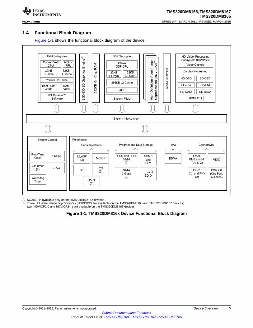
A. SGX530 is available only on the TMS320DM8168 devices.B. Three HD video image coprocessors (HDVICP2) are available on the TMS320DM8168 and TMS320DM8167 devices;
two (HDVICP2-0 and HDVICP2-1) are available on the TMS320DM8165 devices.
TMS320DM8168, TMS320DM8167TMS320DM8165
www.ti.com SPRS614F –MARCH 2011–REVISED MARCH 2015
1.4 Functional Block DiagramFigure 1-1 shows the functional block diagram of the device.
Figure 1-1. TMS320DM816x Device Functional Block Diagram
Copyright © 2011–2015, Texas Instruments Incorporated Device Overview 5Submit Documentation Feedback
Product Folder Links: TMS320DM8168 TMS320DM8167 TMS320DM8165

TMS320DM8168, TMS320DM8167TMS320DM8165SPRS614F –MARCH 2011–REVISED MARCH 2015 www.ti.com
Table of Contents1 Device Overview ......................................... 1 8.2 Reset............................................... 143
1.1 Features .............................................. 1 8.3 Clocking ............................................ 1481.2 Applications........................................... 3 8.4 Interrupts ........................................... 1611.3 Description............................................ 3 9 Peripheral Information and Timings .............. 1731.4 Functional Block Diagram ............................ 5 9.1 Parameter Information ............................. 173
9.2 Recommended Clock and Control Signal Transition2 Revision History ......................................... 7Behavior............................................ 1743 Device Comparison ..................................... 8
9.3 DDR2 and DDR3 Memory Controller .............. 1753.1 Device Characteristics................................ 99.4 Emulation Features and Capability ................ 2113.2 ARM Subsystem .................................... 109.5 Enhanced Direct Memory Access (EDMA)3.3 DSP Subsystem ..................................... 13
Controller........................................... 2153.4 Media Controller..................................... 18
9.6 Ethernet Media Access Controller (EMAC) ........ 2213.5 High-Definition Video Image Coprocessor 2
9.7 General-Purpose Input and Output (GPIO)........ 230(HDVICP2) .......................................... 189.8 General-Purpose Memory Controller (GPMC) and3.6 Inter-Processor Communication..................... 18
Error Locator Module (ELM) ....................... 2333.7 Power, Reset and Clock Management (PRCM)
9.9 High-Definition Multimedia Interface (HDMI) ...... 254Module .............................................. 209.10 High-Definition Video Processing Subsystem3.8 SGX530 (DM8168 only)............................. 26
(HDVPSS).......................................... 2633.9 Memory Map Summary ............................. 27
9.11 Inter-Integrated Circuit (I2C) ....................... 2704 Terminal Configuration and Functions ............ 38
9.12 Multichannel Audio Serial Port (McASP) .......... 2744.1 Pin Assignments .................................... 38
9.13 Multichannel Buffered Serial Port (McBSP)........ 2824.2 Terminal Functions .................................. 56 9.14 Peripheral Component Interconnect Express
5 Specifications ......................................... 116 (PCIe) .............................................. 2855.1 Absolute Maximum Ratings (Unless Otherwise 9.15 Real-Time Clock (RTC) ............................ 290
Noted) .............................................. 116 9.16 Secure Digital and Secure Digital Input Output (SD5.2 ESD Ratings ....................................... 116 and SDIO).......................................... 2925.3 Recommended Operating Conditions ............. 117 9.17 Serial ATA Controller (SATA) ...................... 295Electrical Characteristics Over Recommended Ranges of 9.18 Serial Peripheral Interface (SPI) ................... 299Supply Voltage and Operating Temperature (Unless
9.19 Timers.............................................. 306Otherwise Noted) ......................................... 1199.20 Universal Asynchronous Receiver and Transmitter5.4 Thermal Resistance Characteristics ............... 120
(UART) ............................................. 3096 Device Configurations ............................... 121
9.21 Universal Serial Bus (USB2.0)..................... 3136.1 Control Module..................................... 121 10 Device and Documentation Support.............. 3206.2 Revision Identification ............................. 124
10.1 Device Support..................................... 3206.3 Debugging Considerations......................... 124
10.2 Documentation Support............................ 3216.4 Boot Sequence..................................... 125
10.3 Related Links ...................................... 3226.5 Pin Multiplexing Control............................ 127
10.4 Community Resources............................. 3226.6 How to Handle Unused Pins....................... 134
10.5 Trademarks ........................................ 3227 System Interconnect ................................ 135
10.6 Electrostatic Discharge Caution ................... 3227.1 L3 Interconnect .................................... 135
10.7 Glossary............................................ 3227.2 L4 Interconnect .................................... 138 11 Mechanical Packaging and Orderable
8 Power, Reset, Clocking, and Interrupts .......... 140 Information ............................................. 3238.1 Power Supplies .................................... 140 11.1 Packaging Information ............................. 323
6 Table of Contents Copyright © 2011–2015, Texas Instruments IncorporatedSubmit Documentation Feedback
Product Folder Links: TMS320DM8168 TMS320DM8167 TMS320DM8165

TMS320DM8168, TMS320DM8167TMS320DM8165
www.ti.com SPRS614F –MARCH 2011–REVISED MARCH 2015
2 Revision HistoryNOTE: Page numbers for previous revisions may differ from page numbers in the current version.
Changes from February 1, 2014 to March 17, 2015 (from E Revision (February 2014) to F Revision) Page
• Updated entire document to adhere to Superior Data Manual Standards .................................................... 1• Updated/Changed title from "...Video Processors..." to "...Digital Media Processors..." .................................... 1• Updated/Changed ARM® Cortex™-A8 RISC Processor in Features from "Up to 1.35 GHz" to "Up to 1.20 GHz"...... 1• Updated/Changed C674x™ VLIW DSP in Features from "Up to 1.25 GHz" to "Up to 1 GHz" ............................ 1• Updated/Changed C674x™ VLIW DSP in Features from "Up to 9000 MIPS and 6750 MFLOPS" to "Up to 8000
MIPS and 6000 MFLOPS"........................................................................................................... 1• Updated/Changed CPU Frequency row ......................................................................................... 10• Removed Cycle Time row ......................................................................................................... 10• Updated/Changed Handling Ratings to ESD Ratings ........................................................................ 116• Updated/Changed CVDD Initial Startup NOM from "1.00 or 1.10" to "1.00 or 1.05" ..................................... 117• Updated/Changed CVDD CYG & CYG2 NOM from "0.85-1.10" top "0.85-1.05" ......................................... 117• Added footnote to CVDD CYG & CYG2 NOM value.......................................................................... 117• Updated footnote from "1.10V nominal (for CYG..." to "1.05 nominal (for CYG..." ....................................... 118• Removed FSYSCLK row ......................................................................................................... 118• Removed "AVS Variable Core voltage = 0.8 V" from ICDO and IDDD......................................................... 120• Updated/Changed the System Clocking Overview Figure from "432 MHz" to "audio reference clock" ................ 149• Updated/Changed body of text in PLL Programming Limits ................................................................ 154• Completely updated PLL Clock Frequencies table............................................................................ 155• Completely updated SYSCLK Frequencies table ............................................................................. 156• Completely updated SYSCLK Frequencies table ............................................................................. 157• Updated/Changed tsu(CMDV-CLKH) and th(CLKH-DATV) MIN from "6.0" to "4.1" ................................................... 293• Updated/Changed th(CLKH-CMDIV) and th(CLKH-DATV) MIN from "19.2" to "1.9" .................................................. 293• Added footnote to td(CLKL-CMD) and td(CLKL-DAT) MIN values ..................................................................... 294• Updated/Changed the blank example from "1.0-GHz ARM, 800-MHz DSP" to "930-MHz ARM, 750-MHz DSP".... 321• Updated DEVICE SPEED RANGE in Figure 10-1 ............................................................................ 321• Completely updated Table 10-1 ................................................................................................. 321
Copyright © 2011–2015, Texas Instruments Incorporated Revision History 7Submit Documentation Feedback
Product Folder Links: TMS320DM8168 TMS320DM8167 TMS320DM8165

TMS320DM8168, TMS320DM8167TMS320DM8165SPRS614F –MARCH 2011–REVISED MARCH 2015 www.ti.com
3 Device Comparison
There are variations in the availability of some functions of the TMS320DM816x devices. A comparison ofthe devices, highlighting the differences, is shown in Table 3-1. For more detailed information on thesignificant device features, see Section 3.1, Device Characteristics.
Table 3-1. Device Comparison
DEVICESFEATURES
TMS320DM8168 TMS320DM8167 TMS320DM8165HDVICP2 3 3 2SGX530 Y N N
8 Device Comparison Copyright © 2011–2015, Texas Instruments IncorporatedSubmit Documentation Feedback
Product Folder Links: TMS320DM8168 TMS320DM8167 TMS320DM8165

TMS320DM8168, TMS320DM8167TMS320DM8165
www.ti.com SPRS614F –MARCH 2011–REVISED MARCH 2015
3.1 Device CharacteristicsTable 3-2 provides an overview of the significant features of the TMS320DM816x devices, including thecapacity of on-chip RAM, peripherals, and the package type with pin count.
Table 3-2. Characteristics of the Processor
HARDWARE FEATURES DM8168, DM6187, and DM61851 16-bit and 24-bit HD Capture Channel or
2 8-bit SD Capture Channelsand
1 16-bit HD Capture Channel or2 8-bit SD Capture Channels
andHD Video Processing Subsystem (HDVPSS) 1 16-bit, 24-bit, and 32-bit HD Display Channel
and1 16-bit HD Display Channel
and3 HD and 4 SD Video DACs
and1 HDMI 1.3 Transmitter
DDR2 and DDR3 Memory Controller 2 (32-bit Bus Widths)Asynchronous (8-bit and 16-bit bus width) RAM, NOR,GPMC and ELM NAND
64 Independent ChannelsEDMA 8 QDMA Channels10 Mbps, 100 Mbps, and 1000 Mbps EthernetMAC with Management Data Input and Output 2 (with MII and GMII Interface)Peripherals(MDIO)
Not all peripherals pins are2 (Supports High-Speed and Full-Speed as a Deviceavailable at the same time (for
USB 2.0 and High-Speed, Full-Speed, and Low-Speed as amore detail, see Section 6,Host)Device Configurations).
PCI Express 2.0 1 Port (2 5.0GT per second lanes)7 (32-bit General Purpose)
Timers and1 (Watchdog)
3 (with SIR, MIR, CIR support and RTS and CTS flowUART control)
(UART0 Supports Modem Interface)SPI 1 (Supports 4 slave devices)SD and SDIO 1 (1-bit or 4-bit)I2C 2 (Master or Slave)
3 (1 Six-Serializer and 2 Dual Serializers, Each withMcASP Transmit and Receive and DIT Capability)McBSP 1 (2 Data Pins, Transmit and Receive)Serial ATA (SATA) Supports 2 InterfacesRTC 1GPIO Up to 64 pins
ARM32KB I-cache32KB D-cacheOn-Chip Memory Organization 256KB L2 Cache
64KB RAM48KB Boot ROM
DSP32KB L1 Program (L1P) and Cache (up to 32KB)
32KB L1 Data (L1D) and Cache (up to 32KB)256KB Unified Mapped RAM and Cache (L2)
MEDIA CONTROLLER32KB Shared L1 Cache
256KB L2 RAM
Copyright © 2011–2015, Texas Instruments Incorporated Device Comparison 9Submit Documentation Feedback
Product Folder Links: TMS320DM8168 TMS320DM8167 TMS320DM8165

TMS320DM8168, TMS320DM8167TMS320DM8165SPRS614F –MARCH 2011–REVISED MARCH 2015 www.ti.com
Table 3-2. Characteristics of the Processor (continued)HARDWARE FEATURES DM8168, DM6187, and DM6185
ADDITIONAL SHARED MEMORY512KB On-chip RAM
CPU ID + CPU Rev ID Control Status Register (CSR.[31:16]) 0x1003C674x Megamodule Revision Revision ID Register (MM_REVID[15:0]) 0x0000JTAG BSDL_ID JTAGID Register 0x2B81 E02F
ARM Cortex-A8: 930 MHzBlank
DSP: 750 MHzARM Cortex-A8: 1100 MHz
CPU Frequency (1) MHz 2DSP: 930 MHz
ARM Cortex-A8: 1200 MHz4
DSP: 1000 MHzCore Logic (V) 1.0 V with Required AVS CapabilityUSB Logic (V) 0.9 V
VoltageRAM (V) 1.0 VIO (V) 1.5 V, 1.8 V, 3.3 V
Package 25 x 25 mm 1031-Pin BGA (CYG)Process Technology µm 0.04 µm
Product Preview (PP),Product Status (2) Advance Information (AI), PD
or Production Data (PD)
(1) For more information on the available device speed ranges for each part number, see Table 10-1.(2) PRODUCTION DATA information is current as of publication date. Products conform to specifications per the terms of Texas
Instruments standard warranty. Production processing does not necessarily include testing of all parameters.
3.2 ARM SubsystemThe ARM subsystem is designed to give the ARM Cortex-A8 master control of the device. In general, theARM Cortex-A8 is responsible for configuration and control of the various subsystem, peripherals, andexternal memories.
The ARM subsystem includes the following features:• ARM Cortex-A8 RISC processor:
– ARMv7 ISA plus Thumb®-2, Jazelle-X, and media extensions– NEON floating-point unit– Enhanced memory management unit (MMU)– Little Endian– 32KB L1 instruction cache– 32KB L1 data cache– 256KB L2 cache
• Foresight embedded trace module (ETM)• ARM Cortex-A8 interrupt controller (AINTC)• 64KB internal RAM• 48KB internal public ROM.
10 Device Comparison Copyright © 2011–2015, Texas Instruments IncorporatedSubmit Documentation Feedback
Product Folder Links: TMS320DM8168 TMS320DM8167 TMS320DM8165

ARM Cortex™-A8
NEONETM
256KB L2$
32KB L1I$ 32KB L1D$
Arbiter128
32
ICECrusher
48KB ROM
64KB RAM
ARM Cortex-A8Interrupt Controller
(AINTC)
L3 DMM
32
128
64
64
64 64 128 128
SYSCLK2
128
System EventsDEVOSC
Trace
Debug
TMS320DM8168, TMS320DM8167TMS320DM8165
www.ti.com SPRS614F –MARCH 2011–REVISED MARCH 2015
Figure 3-1. ARM Cortex-A8 Subsystem Block Diagram
3.2.1 ARM Cortex-A8 RISC ProcessorThe ARM Cortex-A8 subsystem integrates the ARM Cortex-A8 processor. The ARM Cortex-A8 processoris a member of ARM Cortex family of general-purpose processors. This processor is targeted at multi-tasking applications where full memory management, high performance, low die size, and low power areall important. The ARM Cortex-A8 processor supports the ARM debug architecture and includes logic toassist in both hardware and software debug. The ARM Cortex-A8 processor has a Harvard architectureand provides a complete high-performance subsystem, including:• ARM Cortex-A8 integer core• Superscalar ARMv7 instruction set• Thumb-2 instruction set• Jazelle RCT acceleration• CP14 debug coprocessor• CP15 system control coprocessor• NEON 64-bit and 128-bit hybrid SIMD engine for multimedia• Enhanced memory management unit (MMU)• Separate level-1 instruction and data caches• Integrated level-2 cache• 128-bit interconnect to system memories and peripherals• Embedded trace module (ETM).
3.2.2 Embedded Trace Module (ETM)To support real-time trace, the ARM Cortex-A8 processor provides an interface to enable connection of anembedded trace module (ETM). The ETM consists of two parts:• The Trace port provides real-time trace capability for the ARM Cortex-A8.• Triggering facilities provide trigger resources, which include address and data comparators, counter,
and sequencers.
The ARM Cortex-A8 trace port is connected to the system-level embedded trace buffer (ETB). The ETBhas a 32KB buffer memory. ETB enabled debug tools are required to read and interpret the captured tracedata.
For more details on the ETB, see Section 9.4.2.
Copyright © 2011–2015, Texas Instruments Incorporated Device Comparison 11Submit Documentation Feedback
Product Folder Links: TMS320DM8168 TMS320DM8167 TMS320DM8165

TMS320DM8168, TMS320DM8167TMS320DM8165SPRS614F –MARCH 2011–REVISED MARCH 2015 www.ti.com
3.2.3 ARM Cortex-A8 Interrupt Controller (AINTC)The ARM Cortex-A8 subsystem contains an interrupt controller (AINTC) that prioritizes all service requestsfrom the system peripherals and generates either IRQ or FIQ to the ARM Cortex-A8 processor. For moredetails on the AINTC, see Section 8.4.
3.2.4 System InterconnectThe ARM Cortex-A8 processor in connected through the arbiter to both an L3 interconnect port and aDMM port. The DMM port is 128-bits wide and provides the ARM Cortex-A8 direct access to the DDRmemories, while the L3 interconnect port is 64-bits wide and provides access to the remaining devicemodules.
12 Device Comparison Copyright © 2011–2015, Texas Instruments IncorporatedSubmit Documentation Feedback
Product Folder Links: TMS320DM8168 TMS320DM8167 TMS320DM8165

Instruction Fetch
C674x+ CPU
RegisterFile A
RegisterFile B
Cache Control
Memory Protect
Bandwidth Mgmt
L1P
256
Cache Control
Memory Protect
Bandwidth Mgmt
L1D
64 64
8 x 32
32K BytesL1D RAM
and Cache
32K BytesL1P RAM
and Cachewith EDC
256
Cache Control
Memory Protect
Bandwidth Mgmt
L2
256K BytesL2 RAM
with ECC
256
HDVICP2 HostSL2 Port
256
CFG
MDMA SDMA
EMC
Power Down
InterruptController
IDMA
256
256
256
256
256
128
High-PerformanceSwitch Fabric
128
Peripherals32
TMS320DM8168, TMS320DM8167TMS320DM8165
www.ti.com SPRS614F –MARCH 2011–REVISED MARCH 2015
3.3 DSP SubsystemThe DSP Subsystem includes the following features:• C674x DSP CPU• 32KB L1 Program (L1P) and Cache (up to 32KB) with Error Detection Code (EDC)• 32KB L1 Data (L1D) and Cache (up to 32KB)• 256KB L2 Unified Mapped RAM and Cache with Error Correction Code (ECC)• Direct Connection to the HDVICP2 Host SL2 Port for HDVICP2-0 and HDVICP2-1• Little endian
Figure 3-2. C674x Megamodule Block Diagram
Copyright © 2011–2015, Texas Instruments Incorporated Device Comparison 13Submit Documentation Feedback
Product Folder Links: TMS320DM8168 TMS320DM8167 TMS320DM8165

TMS320DM8168, TMS320DM8167TMS320DM8165SPRS614F –MARCH 2011–REVISED MARCH 2015 www.ti.com
3.3.1 C674x DSP CPU DescriptionThe C674x central processing unit (CPU) consists of eight functional units, two register files, and two datapaths as shown in Figure 3-3. The two general-purpose register files (A and B) each contain 32 32-bitregisters for a total of 64 registers. The general-purpose registers can be used for data or can be dataaddress pointers. The data types supported include packed 8-bit data, packed 16-bit data, 32-bit data, 40-bit data, and 64-bit data. Values larger than 32 bits, such as 40-bit-long or 64-bit-long values are stored inregister pairs, with the 32 LSBs of data placed in an even register and the remaining 8 or 32 MSBs in thenext upper register (which is always an odd-numbered register).
The eight functional units (.M1, .L1, .D1, .S1, .M2, .L2, .D2, and .S2) are each capable of executing oneinstruction every clock cycle. The .M functional units perform all multiply operations. The .S and .L unitsperform a general set of arithmetic, logical, and branch functions. The .D units primarily load data frommemory to the register file and store results from the register file into memory.
The C674x CPU combines the performance of the C64x+ core with the floating-point capabilities of theC67x+ core.
Each C674x .M unit can perform one of the following each clock cycle: one 32 x 32 bit multiply, one 16 x32 bit multiply, two 16 x 16 bit multiplies, two 16 x 32 bit multiplies, two 16 x 16 bit multiplies with add andsubtract capabilities, four 8 x 8 bit multiplies, four 8 x 8 bit multiplies with add operations, and four 16 x 16multiplies with add and subtract capabilities (including a complex multiply). There is also support for Galoisfield multiplication for 8-bit and 32-bit data. Many communications algorithms such as FFTs and modemsrequire complex multiplication. The complex multiply (CMPY) instruction takes for 16-bit inputs andproduces a 32-bit real and a 32-bit imaginary output. There are also complex multiplies with roundingcapability that produces one 32-bit packed output that contain 16-bit real and 16-bit imaginary values. The32 x 32 bit multiply instructions provide the extended precision necessary for high-precision algorithms ona variety of signed and unsigned 32-bit data types.
The .L or (Arithmetic Logic Unit) now incorporates the ability to do parallel add and subtract operations ona pair of common inputs. Versions of this instruction exist to work on 32-bit data or on pairs of 16-bit dataperforming dual 16-bit add and subtracts in parallel. There are also saturated forms of these instructions.
The C674x core enhances the .S unit in several ways. On the previous cores, dual 16-bit MIN2 and MAX2comparisons were only available on the .L units. On the C674x core they are also available on the .S unitwhich increases the performance of algorithms that do searching and sorting. Finally, to increase datapacking and unpacking throughput, the .S unit allows sustained high performance for the quad 8-bit and16-bit and dual 16-bit instructions. Unpack instructions prepare 8-bit data for parallel 16-bit operations.Pack instructions return parallel results to output precision including saturation support.
Other new features include:• SPLOOP - A small instruction buffer in the CPU that aids in creation of software pipelining loops where
multiple iterations of a loop are executed in parallel. The SPLOOP buffer reduces the code sizeassociated with software pipelining. Furthermore, loops in the SPLOOP buffer are fully interruptible.
• Compact Instructions - The native instruction size for the C6000 devices is 32 bits. Many commoninstructions such as MPY, AND, OR, ADD, and SUB can be expressed as 16 bits if the C674xcompiler can restrict the code to use certain registers in the register file. This compression isperformed by the code generation tools.
• Instruction Set Enhancement - As noted above, there are new instructions such as 32-bitmultiplications, complex multiplications, packing, sorting, bit manipulation, and 32-bit Galois fieldmultiplication.
• Exceptions Handling - Intended to aid the programmer in isolating bugs. The C674x CPU is able todetect and respond to exceptions, both from internally detected sources (such as illegal op-codes) andfrom system events (such as a watchdog time expiration).
• Privilege - Defines user and supervisor modes of operation, allowing the operating system to give abasic level of protection to sensitive resources. Local memory is divided into multiple pages, each withread, write, and execute permissions.
14 Device Comparison Copyright © 2011–2015, Texas Instruments IncorporatedSubmit Documentation Feedback
Product Folder Links: TMS320DM8168 TMS320DM8167 TMS320DM8165
TMS320DM8168, TMS320DM8167TMS320DM8165
www.ti.com SPRS614F –MARCH 2011–REVISED MARCH 2015
• Time-Stamp Counter - Primarily targeted for Real-Time Operating System (RTOS) robustness, a free-running time-stamp counter is implemented in the CPU which is not sensitive to system stalls.
For more details on the C674x CPU and its enhancements over the C64x architecture, see the followingdocuments:• TMS320C674x DSP CPU and Instruction Set User's Guide (literature number SPRUFE8)• TMS320C674x DSP Megamodule Reference Guide (literature number SPRUFK5)
Copyright © 2011–2015, Texas Instruments Incorporated Device Comparison 15Submit Documentation Feedback
Product Folder Links: TMS320DM8168 TMS320DM8167 TMS320DM8165

src2
src2
.D1
.M1
.S1
.L1
long src
odd dst
src2
src1
src1
src1
src1
even dst
even dst
odd dst
dst1
dst
src2
src2
src2
long src
DA1
ST1b
LD1b
LD1a
ST1a
Data path A
Oddregister
file A(A1, A3,
A5...A31)
Oddregisterfile B
(B1, B3,B5...B31)
.D2src1
dst
src2DA2
LD2a
LD2b
src2
.M2 src1
dst1
.S2
src1
even dst
long src
odd dst
ST2a
ST2b
long src
.L2
even dst
odd dst
src1
Data path B
Control Register
32 MSB
32 LSB
dst2
32 MSB
32 LSB
2x
1x
32 LSB
32 MSB
32 LSB
32 MSB
dst2
8
8
8
8
32
32
32
32
Evenregister
file A(A0, A2,
A4...A30)
Evenregisterfile B
(B0, B2,B4...B30)
(D)
A. .M unit, is 32 MSB.B On .M unit, is 32 LSB.C. On C64x CPU .M unit, is 32 bits; on C64x+ CPU .M unit, is 64 bits.D. On .L and .S units, connects to odd register files and even connects to even register files
dst2dst1
src2 src2odd dst dst
(D)
(A)
(B)
(C)
(C)
(B)
(A)
(D)
(D)
TMS320DM8168, TMS320DM8167TMS320DM8165SPRS614F –MARCH 2011–REVISED MARCH 2015 www.ti.com
Figure 3-3. TMS320C674x CPU (DSP Core) Data Paths
16 Device Comparison Copyright © 2011–2015, Texas Instruments IncorporatedSubmit Documentation Feedback
Product Folder Links: TMS320DM8168 TMS320DM8167 TMS320DM8165

TMS320DM8168, TMS320DM8167TMS320DM8165
www.ti.com SPRS614F –MARCH 2011–REVISED MARCH 2015
3.3.2 System Memory Management Unit (System MMU)All C674x DSP accesses through the MDMA port are directed through the system memory managementunit (System MMU) module where they are remapped to physical system addresses. This protects theARM Cortex-A8 memory regions from accidental corruption by C674x code and allows for direct allocationof buffers in user space without the need for translation between ARM and DSP applications.
In addition, accesses by the EDMA TC0 may optionally be routed through the System MMU. This allowsEDMA Channel 0 to be used by the DSP to perform transfers using only the known virtual addresses ofthe associated buffers. The MMU_CFG register in the Control Module is used to enable and disable use ofthe DSP EDMA MMU by the EDMA TC.
For details on the System MMU features and registers, see the System MMU chapter of theTMS320DM816x DaVinci Digital Media Processors Technical Reference Manual (literature numberSPRUGX8).
3.3.2.1 System MMU Registers
Table 3-3 lists the System MMU registers.
Table 3-3. System MMU Registers Summary
HEX ADDRESS ACRONYM REGISTER NAME0x4801 0000h MMU_REVISION Revision0x4801 0010h MMU_SYSCONFIG Configuration0x4801 0014h MMU_SYSSTATUS Status0x4801 0018h MMU_IRQSTATUS IRQ Status0x4801 001Ch MMU_IRQENABLE IRQ Enable0x4801 0040h MMU_WALKING_ST Table Walking Logic0x4801 0044h MMU_CNTL Control0x4801 0048h MMU_FAULT_AD Fault Address0x4801 004Ch MMU_TTB Translation Table Base Address0x4801 0050h MMU_LOCK Lock0x4801 0054h MMU_LD_TLB Load0x4801 0058h MMU_CAM CAM0x4801 005Ch MMU_RAM RAM0x4801 0060h MMU_GFLUSH Global Flush0x4801 0064h MMU_FLUSH_ENTRY Flush Entry0x4801 0068h MMU_READ_CAM Read CAM0x4801 006Ch MMU_READ_RAM Read RAM0x4801 0070h MMU_EMU_FAULT_AD EMU Fault Address0x4801 0080h MMU_FAULT_PC Fault Program Counter
Copyright © 2011–2015, Texas Instruments Incorporated Device Comparison 17Submit Documentation Feedback
Product Folder Links: TMS320DM8168 TMS320DM8167 TMS320DM8165

TMS320DM8168, TMS320DM8167TMS320DM8165SPRS614F –MARCH 2011–REVISED MARCH 2015 www.ti.com
3.4 Media ControllerThe Media Controller has the responsibility of managing the HDVPSS and HDVICP2 modules.
3.5 High-Definition Video Image Coprocessor 2 (HDVICP2)The HDVICP2 is a video encoder and decoder hardware accelerator supporting a range of encode anddecode operations at up to 1080p60 for most major video codec standards. Transcode operations are alsosupported. The main video codec standards supported in hardware are MPEG1, MPEG2 and MPEG4ASP and SP, H.264 BL, MP, and HP, VC-1 SP, MP, and AP, RV9 and RV10, AVS-1.0, and ON2 VP6.2and VP7. The HDVICP2 hardware accelerator is composed of the following elements:• Motion estimation acceleration engine• Loop filter acceleration engine• Two RISC processors and associated memory used for algorithmic decision making and control• Intra-prediction estimation engine• Calculation engine• Motion compensation engine• Entropy coder and decoder• Video DMA• Synchronization boxes• Shared L2 controller• Local interconnect.
3.6 Inter-Processor CommunicationThis device is a multi-core device that requires software to efficiently manage and communicate betweenthe cores. The following are the main features that need to be implemented by such software:1. Device management of the slave processors from the host processor.2. Inter-processor communication between the cores for transfer and exchange of information between
them.
On this device, the host processor is usually the ARM Cortex-A8. This processor is responsible forbootloading the slave processors (C674x). Bootloading includes power management of the slaves(powerup and powerdown and other power management), reset control (reset and release of the slaveprocessor) and setting the entry point of the slave executable into the appropriate register. This device hasa power-on reset (POR) and warm reset. For the POR reset, the ARM Cortex-A8 is taken out of reset andit boots from its boot ROM. Once booted, the ARM Cortex-A8 bootloads the C674x processor.
For implementing efficient inter-processor communication between the multiple cores on the device, thefollowing hardware features are provided:• Mailbox interrupts• Hardware spinlocks
Mailboxes provide a mechanism for one processor to write a value to a register and send an interrupt toanother processor. Spinlocks facilitate access to shared resources in the system.
3.6.1 Mailbox ModuleThe device Mailbox module facilitates communication between the ARM Cortex-A8, C674x DSP, and theMedia Controller. It consists of twelve mailboxes, each supporting communication between two of theabove processors. The sender sends information to the receiver by writing a message to the mailboxregisters. Interrupt signaling is used to notify the receiver that a message has been queued or to notify thesender about an overflow situation.
The Mailbox module supports the following features (see Figure 3-4):• 12 mailboxes
18 Device Comparison Copyright © 2011–2015, Texas Instruments IncorporatedSubmit Documentation Feedback
Product Folder Links: TMS320DM8168 TMS320DM8167 TMS320DM8165
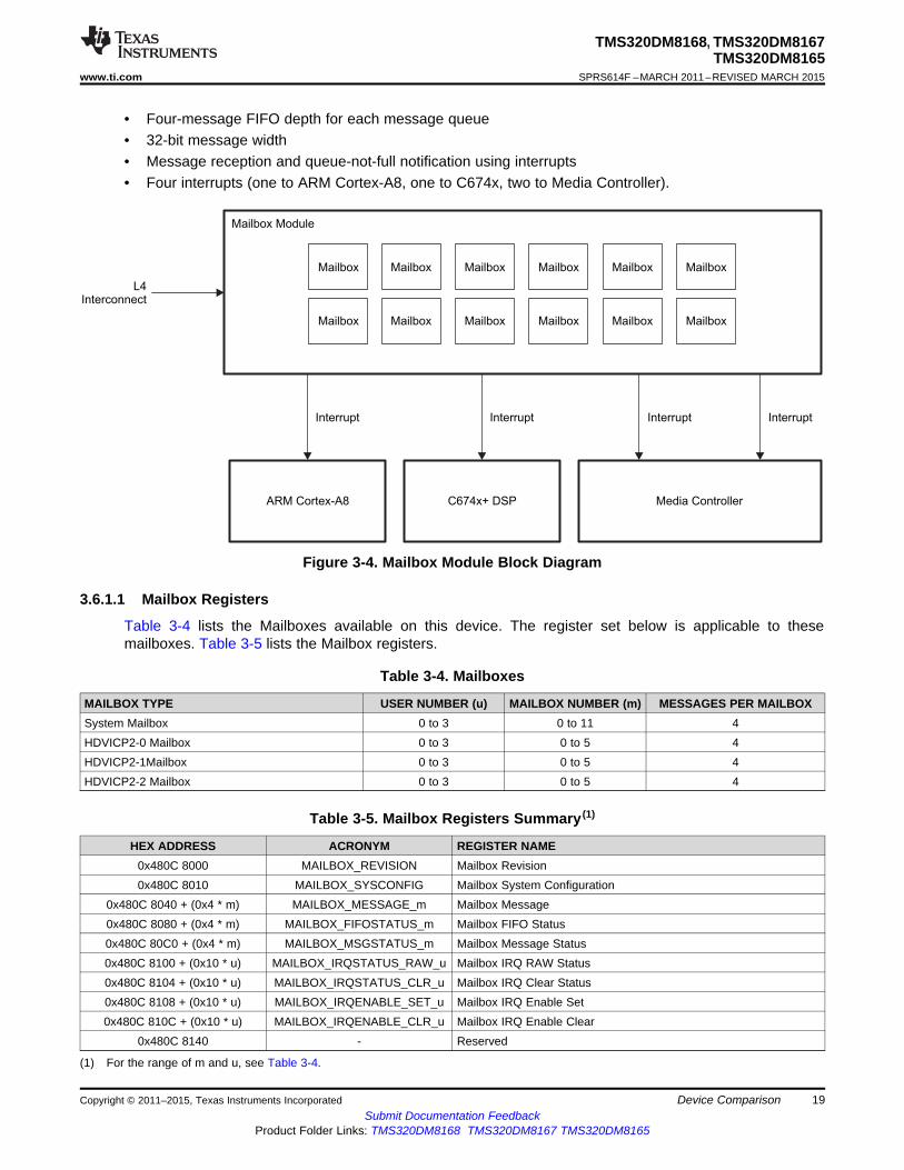
Mailbox Mailbox Mailbox Mailbox Mailbox Mailbox
Mailbox Mailbox Mailbox Mailbox Mailbox Mailbox
L4Interconnect
Interrupt Interrupt Interrupt Interrupt
Mailbox Module
ARM Cortex-A8 C674x+ DSP Media Controller
TMS320DM8168, TMS320DM8167TMS320DM8165
www.ti.com SPRS614F –MARCH 2011–REVISED MARCH 2015
• Four-message FIFO depth for each message queue• 32-bit message width• Message reception and queue-not-full notification using interrupts• Four interrupts (one to ARM Cortex-A8, one to C674x, two to Media Controller).
Figure 3-4. Mailbox Module Block Diagram
3.6.1.1 Mailbox Registers
Table 3-4 lists the Mailboxes available on this device. The register set below is applicable to thesemailboxes. Table 3-5 lists the Mailbox registers.
Table 3-4. Mailboxes
MAILBOX TYPE USER NUMBER (u) MAILBOX NUMBER (m) MESSAGES PER MAILBOXSystem Mailbox 0 to 3 0 to 11 4HDVICP2-0 Mailbox 0 to 3 0 to 5 4HDVICP2-1Mailbox 0 to 3 0 to 5 4HDVICP2-2 Mailbox 0 to 3 0 to 5 4
Table 3-5. Mailbox Registers Summary (1)
HEX ADDRESS ACRONYM REGISTER NAME0x480C 8000 MAILBOX_REVISION Mailbox Revision0x480C 8010 MAILBOX_SYSCONFIG Mailbox System Configuration
0x480C 8040 + (0x4 * m) MAILBOX_MESSAGE_m Mailbox Message0x480C 8080 + (0x4 * m) MAILBOX_FIFOSTATUS_m Mailbox FIFO Status0x480C 80C0 + (0x4 * m) MAILBOX_MSGSTATUS_m Mailbox Message Status0x480C 8100 + (0x10 * u) MAILBOX_IRQSTATUS_RAW_u Mailbox IRQ RAW Status0x480C 8104 + (0x10 * u) MAILBOX_IRQSTATUS_CLR_u Mailbox IRQ Clear Status0x480C 8108 + (0x10 * u) MAILBOX_IRQENABLE_SET_u Mailbox IRQ Enable Set0x480C 810C + (0x10 * u) MAILBOX_IRQENABLE_CLR_u Mailbox IRQ Enable Clear
0x480C 8140 - Reserved
(1) For the range of m and u, see Table 3-4.
Copyright © 2011–2015, Texas Instruments Incorporated Device Comparison 19Submit Documentation Feedback
Product Folder Links: TMS320DM8168 TMS320DM8167 TMS320DM8165

TMS320DM8168, TMS320DM8167TMS320DM8165SPRS614F –MARCH 2011–REVISED MARCH 2015 www.ti.com
3.6.2 Spinlock ModuleThe Spinlock module provides hardware assistance for synchronizing the processes running on multipleprocessors in the device:• ARM Cortex-A8 processor• C674x DSP• Media Controller processors.
The Spinlock module implements 64 spinlocks (or hardware semaphores) that provide an efficient way toperform a lock operation of a device resource using a single read-access, avoiding the need for a read-modify-write bus transfer of which the programmable cores are not capable.
3.6.2.1 Spinlock Registers
Table 3-6. Spinlock Registers Summary (1)
HEX ADDRESS ACRONYM REGISTER NAME0x480C A000 SPINLOCK_REV Revision0x480C A010h SPINLOCK_SYSCFG System Configuration0x480C A014h SPINLOCK_SYSSTAT System Status
0x480C A800 + (0x4*i) SPINLOCK_LOCK_REG_i Lock
(1) i = 0 to 63
3.7 Power, Reset and Clock Management (PRCM) ModuleThe PRCM module is the centralized management module for the power, reset, and clock control signalsof the device. It interfaces with all the components on the device for power, clock, and reset managementthrough power-control signals. It integrates enhanced features to allow the device to adapt energyconsumption dynamically, according to changing application and performance requirements. Theinnovative hardware architecture allows a substantial reduction in leakage current.
The PRCM module is composed of two main entities:• Power reset manager (PRM): Handles the power, reset, wake-up management, and system clock
source control (oscillator)• Clock manager (CM): Handles the clock generation, distribution, and management.
Table 3-7 lists the physical addresses of the PRM and CM modules. Table 3-8 through Table 3-25 provideregister mapping summaries of the PRM and CM registers.
For more details on the PRCM, see Section 8 of this data sheet, Power, Reset, Clocking and Interrupts,and the PRCM chapter of the TMS320DM816x DaVinci Digital Media Processors Technical ReferenceManual (literature number SPRUGX8).
Table 3-7. PRCM Register Address Summary
ADDRESS OFFSET MODULE NAME SIZE SEE0x0000 PRM_DEVICE 256 Bytes Table 3-80x0100 CM_DEVICE 256 Bytes Table 3-90x0300 CM_DPLL 256 Bytes Table 3-110x0400 CM_ACTIVE 256 Bytes Table 3-120x0500 CM_DEFAULT 256 Bytes Table 3-130x0600 CM_IVAHD0 256 Bytes Table 3-140x0700 CM_IVAHD1 256 Bytes Table 3-150x0800 CM_IVAHD2 256 Bytes Table 3-160x0900 CM_SGX 256 Bytes Table 3-170x0A00 PRM_ACTIVE 256 Bytes Table 3-18
20 Device Comparison Copyright © 2011–2015, Texas Instruments IncorporatedSubmit Documentation Feedback
Product Folder Links: TMS320DM8168 TMS320DM8167 TMS320DM8165

TMS320DM8168, TMS320DM8167TMS320DM8165
www.ti.com SPRS614F –MARCH 2011–REVISED MARCH 2015
Table 3-7. PRCM Register Address Summary (continued)ADDRESS OFFSET MODULE NAME SIZE SEE
0x0B00 PRM_DEFAULT 256 Bytes Table 3-190x0C00 PRM_IVAHD0 256 Bytes Table 3-200x0D00 PRM_IVAHD1 256 Bytes Table 3-210x0E00 PRM_IVAHD2 256 Bytes Table 3-220x0F00 PRM_SGX 256 Bytes Table 3-230x1400 CM_ALWON 1 KBytes Table 3-240x1800 PRM_ALWON 1 KBytes Table 3-25
Table 3-8. PRM_DEVICE Register Summary
HEX ADDRESS ACRONYM REGISTER NAME0x4818 00A0 PRM_RSTCTRL Global software cold and warm reset control0x4818 00A4 PRM_RSTTIME Reset duration control0x4818 00A8 PRM_RSTST Global reset sources log
Table 3-9. CM_DEVICE Register Summary
HEX ADDRESS ACRONYM REGISTER NAME0x4818 0100 CM_CLKOUT_CTRL SYS_CCCLKOUT output control
Table 3-10. OCP_SOCKET_PRM Register Summary
HEX ADDRESS ACRONYM REGISTER NAME0x4818 0200 REVISION_PRM PRCM IP revision code
Table 3-11. CM_DPLL Register Summary
HEX ADDRESS ACRONYM REGISTER NAME0x4818 0300 CM_SYSCLK1_CLKSEL SYSCLK1 clock divider value select0x4818 0304 CM_SYSCLK2_CLKSEL SYSCLK2 clock divider value select0x4818 0308 CM_SYSCLK3_CLKSEL SYSCLK3 clock divider value select0x4818 030C CM_SYSCLK4_CLKSEL SYSCLK4 clock divider value select0x4818 0310 CM_SYSCLK5_CLKSEL SYSCLK5 clock divider value select0x4818 0314 CM_SYSCLK6_CLKSEL SYSCLK6 clock divider value select0x4818 0318 CM_SYSCLK7_CLKSEL SYSCLK7 clock divider value select0x4818 0324 CM_SYSCLK10_CLKSEL SYSCLK10 clock divider value select0x4818 032C CM_SYSCLK11_CLKSEL SYSCLK11 clock divider value select0x4818 0334 CM_SYSCLK13_CLKSEL SYSCLK13 clock divider value select0x4818 0338 CM_SYSCLK15_CLKSEL SYSCLK15 clock divider value select0x4818 0340 CM_VPB3_CLKSEL Video PLL B3 clock divider value select0x4818 0344 CM_VPC1_CLKSEL Video PLL C1 clock divider value select0x4818 0348 CM_VPD1_CLKSEL Video PLL D1 clock divider value select0x4818 034C CM_SYSCLK19_CLKSEL SYSCLK19 clock divider value select0x4818 0350 CM_SYSCLK20_CLKSEL SYSCLK20 clock divider value select0x4818 0354 CM_SYSCLK21_CLKSEL SYSCLK21 clock divider value select0x4818 0358 CM_SYSCLK22_CLKSEL SYSCLK22 clock divider value select0x4818 035C CM_APA_CLKSEL Audio PLL A clock divider value select0x4818 0370 CM_SYSCLK14_CLKSEL SYSCLK14 clock mux select line0x4818 0374 CM_SYSCLK16_CLKSEL SYSCLK16 clock mux select line0x4818 0378 CM_SYSCLK18_CLKSEL SYSCLK18 clock mux select line
Copyright © 2011–2015, Texas Instruments Incorporated Device Comparison 21Submit Documentation Feedback
Product Folder Links: TMS320DM8168 TMS320DM8167 TMS320DM8165

TMS320DM8168, TMS320DM8167TMS320DM8165SPRS614F –MARCH 2011–REVISED MARCH 2015 www.ti.com
Table 3-11. CM_DPLL Register Summary (continued)HEX ADDRESS ACRONYM REGISTER NAME
0x4818 037C CM_AUDIOCLK_MCASP0_CLKSEL McASP0 audio clock mux select line0x4818 0380 CM_AUDIOCLK_MCASP1_CLKSEL McASP1 audio clock mux select line0x4818 0384 CM_AUDIOCLK_MCASP2_CLKSEL McASP2 audio clock mux select line0x4818 0388 CM_AUDIOCLK_MCBSP_CLKSEL McBSP audio clock mux select line0x4818 0390 CM_TIMER1_CLKSEL Timer1 clock mux select line0x4818 0394 CM_TIMER2_CLKSEL Timer2 clock mux select line0x4818 0398 CM_TIMER3_CLKSEL Timer3 clock mux select line0x4818 039C CM_TIMER4_CLKSEL Timer4 clock mux select line0x4818 03A0 CM_TIMER5_CLKSEL Timer5 clock mux select line0x4818 03A4 CM_TIMER6_CLKSEL Timer6 clock mux select line0x4818 03A8 CM_TIMER7_CLKSEL Timer7 clock mux select line0x4818 03B0 CM_SYSCLK23_CLKSEL SYSCLK23 clock divider value select0x4818 03B4 CM_SYSCLK24_CLKSEL SYSCLK24 clock divider value select
Table 3-12. CM_ACTIVE Register Summary
HEX ADDRESS ACRONYM REGISTER NAME0x4818 0400 CM_GEM_CLKSTCTRL DSP clock domain power state transition0x4818 0404 CM_HDDSS_CLKSTCTRL HDVPSS clock domain power state transition0x4818 0408 CM_HDMI_CLKSTCTRL HDMI clock domain power state transition0x4818 0420 CM_ACTIVE_GEM_CLKCTRL DSP clock management control0x4818 0424 CM_ACTIVE_HDDSS_CLKCTRL HDVPSS clock management control0x4818 0428 CM_ACTIVE_HDMI_CLKCTRL HDMI clock management control
Table 3-13. CM_DEFAULT Register Summary
HEX ADDRESS ACRONYM REGISTER NAME0x4818 0504 CM_DEFAULT_L3_MED_CLKSTCTRL L3 clock domain power state transition0x4818 0508 CM_DEFAULT_L3_FAST_CLKSTCTRL L3 clock domain power state transition0x4818 0510 CM_DEFAULT_PCI_CLKSTCTRL PCI clock domain power state transition0x4818 0514 CM_DEFAULT_L3_SLOW_CLKSTCTRL L3 clock domain power state transition0x4818 0520 CM_DEFAULT_EMIF_0_CLKCTRL EMIF0 clock management control0x4818 0524 CM_DEFAULT_EMIF_1_CLKCTRL EMIF1 clock management control0x4818 0528 CM_DEFAULT_DMM_CLKCTRL DMM clock management control0x4818 052C CM_DEFAULT_FW_CLKCTRL EMIF FW clock management control0x4818 0558 CM_DEFAULT_USB_CLKCTRL USB clock management control0x4818 0560 CM_DEFAULT_SATA_CLKCTRL SATA clock management control0x4818 0578 CM_DEFAULT_PCI_CLKCTRL PCI clock management control
Table 3-14. CM_IVAHD0 Register Summary
HEX ADDRESS ACRONYM REGISTER NAME0x4818 0600 CM_IVAHD0_CLKSTCTRL HDVICP2-0 clock domain power state transition0x4818 0620 CM_IVAHD0_IVAHD_CLKCTRL HDVICP2-0 clock management control0x4818 0624 CM_IVAHD0_SL2_CLKCTRL HDVICP2-0 SL2 clock management control
22 Device Comparison Copyright © 2011–2015, Texas Instruments IncorporatedSubmit Documentation Feedback
Product Folder Links: TMS320DM8168 TMS320DM8167 TMS320DM8165

TMS320DM8168, TMS320DM8167TMS320DM8165
www.ti.com SPRS614F –MARCH 2011–REVISED MARCH 2015
Table 3-15. CM_IVAHD1 Register Summary
HEX ADDRESS ACRONYM REGISTER NAME0x4818 0700 CM_IVAHD1_CLKSTCTRL HDVICP2-1 clock domain power state transition0x4818 0720 CM_IVAHD1_IVAHD_CLKCTRL HDVICP2-1 clock management control0x4818 0724 CM_IVAHD1_SL2_CLKCTRL HDVICP2-1 SL2 clock management control
Table 3-16. CM_IVAHD2 Register Summary
HEX ADDRESS ACRONYM REGISTER NAME0x4818 0800 CM_IVAHD2_CLKSTCTRL HDVICP2-2 clock domain power state transition0x4818 0820 CM_IVAHD2_IVAHD_CLKCTRL HDVICP2-2 clock management control0x4818 0824 CM_IVAHD2_SL2_CLKCTRL HDVICP2-2 SL2 clock management control
Table 3-17. CM_SGX Register Summary
HEX ADDRESS ACRONYM REGISTER NAME0x4818 0900 CM_SGX_CLKSTCTRL SGX530 clock domain power state transition0x4818 0920 CM_SGX_SGX_CLKCTRL SGX530 clock management control
Table 3-18. PRM_ACTIVE Register Summary
HEX ADDRESS ACRONYM REGISTER NAME0x4818 0A00 PM_ACTIVE_PWRSTCTRL Active power state control0x4818 0A04 PM_ACTIVE_PWRSTST Active power domain state status0x4818 0A10 RM_ACTIVE_RSTCTRL Active domain reset control release0x4818 0A14 RM_ACTIVE_RSTST Active domain reset source log
Table 3-19. PRM_DEFAULT Register Summary
HEX ADDRESS ACRONYM REGISTER NAME0x4818 0B00 PM_DEFAULT_PWRSTCTRL Default power state0x4818 0B04 PM_DEFAULT_PWRSTST Default power domain state 0 status0x4818 0B10 RM_DEFAULT_RSTCTRL Default subsystem reset control release0x4818 0B14 RM_DEFAULT_RSTST Default domain reset source log
Table 3-20. PRM_IVAHD0 Register Summary
HEX ADDRESS ACRONYM REGISTER NAME0x4818 0C00 PM_IVAHD0_PWRSTCTRL HDVICP2-0 power state control0x4818 0C04 PM_IVAHD0_PWRSTST HDVICP2-0 power domain state status0x4818 0C10 RM_IVAHD0_RSTCTRL HDVICP2-0 subsystem reset control release0x4818 0C14 RM_IVAHD0_RSTST HDVICP2-0 domain reset source log
Table 3-21. PRM_IVAHD1 Register Summary
HEX ADDRESS ACRONYM REGISTER NAME0x4818 0D00 PM_IVAHD1_PWRSTCTRL HDVICP2-1 power state control0x4818 0D04 PM_IVAHD1_PWRSTST HDVICP2-1 power domain state status0x4818 0D10 RM_IVAHD1_RSTCTRL HDVICP2-1 subsystem reset control release0x4818 0D14 RM_IVAHD1_RSTST HDVICP2-1 domain reset source log
Copyright © 2011–2015, Texas Instruments Incorporated Device Comparison 23Submit Documentation Feedback
Product Folder Links: TMS320DM8168 TMS320DM8167 TMS320DM8165

TMS320DM8168, TMS320DM8167TMS320DM8165SPRS614F –MARCH 2011–REVISED MARCH 2015 www.ti.com
Table 3-22. PRM_IVAHD2 Register Summary
HEX ADDRESS ACRONYM REGISTER NAME0x4818 0E00 PM_IVAHD2_PWRSTCTRL HDVICP2-2 power state control0x4818 0E04 PM_IVAHD2_PWRSTST HDVICP2-2 power domain state status0x4818 0E10 RM_IVAHD2_RSTCTRL HDVICP2-2 subsystem reset control release0x4818 0E14 RM_IVAHD2_RSTST HDVICP2-2 domain reset source log
Table 3-23. PRM_SGX Register Summary
HEX ADDRESS ACRONYM REGISTER NAME0x4818 0F00 PM_SGX_PWRSTCTRL SGX530 power state control0x4818 0F04 RM_SGX_RSTCTRL SGX530 domain reset control release0x4818 0F10 PM_SGX_PWRSTST SGX530 power domain state status0x4818 0F14 RM_SGX_RSTST SGX530 domain reset source log
Table 3-24. CM_ALWON Register Summary
HEX ADDRESS ACRONYM REGISTER NAME0x4818 1400 CM_ALWON_L3_SLOW_CLKSTCTRL L3 clock domain power state transition0x4818 1404 CM_ETHERNET_CLKSTCTRL EMAC clock domain power state transition0x4818 1408 CM_ALWON_L3_MED_CLKSTCTRL L3 clock domain power state transition0x4818 140C CM_MMU_CLKSTCTRL MMU clock domain power state transition0x4818 1410 CM_MMUCFG_CLKSTCTRL MMU CFG clock domain power state transition0x4818 1414 CM_ALWON_OCMC_0_CLKSTCTRL OCMC 0 clock domain power state transition0x4818 1418 CM_ALWON_OCMC_1_CLKSTCTRL OCMC 1 clock domain power state transition0x4818 141C CM_ALWON_MPU_CLKSTCTRL Processor clock domain power state transition0x4818 1420 CM_ALWON_SYSCLK4_CLKSTCTRL SYSCLK4 clock domain power state transition0x4818 1424 CM_ALWON_SYSCLK5_CLKSTCTRL SYSCLK5 clock domain power state transition0x4818 1428 CM_ALWON_SYSCLK6_CLKSTCTRL SYSCLK6 clock domain power state transition0x4818 142C CM_ALWON_RTC_CLKSTCTRL RTC clock domain power state transition0x4818 1430 CM_ALWON_L3_FAST_CLKSTCTRL L3 clock domain power state transition0x4818 1540 CM_ALWON_MCASP0_CLKCTRL McASP 0 clock management control0x4818 1544 CM_ALWON_MCASP1_CLKCTRL McASP 1 clock management control0x4818 1548 CM_ALWON_MCASP2_CLKCTRL McASP 2 clock management control0x4818 154C CM_ALWON_MCBSP_CLKCTRL McBSP clock management control0x4818 1550 CM_ALWON_UART_0_CLKCTRL UART 0 clock management control0x4818 1554 CM_ALWON_UART_1_CLKCTRL UART 1 clock management control0x4818 1558 CM_ALWON_UART_2_CLKCTRL UART 2 clock management control0x4818 155C CM_ALWON_GPIO_0_CLKCTRL GPIO 0 clock management control0x4818 1560 CM_ALWON_GPIO_1_CLKCTRL GPIO 1 clock management control0x4818 1564 CM_ALWON_I2C_0_CLKCTRL I2C 0 clock management control0x4818 1568 CM_ALWON_I2C_1_CLKCTRL I2C 1 clock management control0x4818 1570 CM_ALWON_TIMER_1_CLKCTRL Timer1 clock management control0x4818 1574 CM_ALWON_TIMER_2_CLKCTRL Timer2 clock management control0x4818 1578 CM_ALWON_TIMER_3_CLKCTRL Timer3 clock management control0x4818 157C CM_ALWON_TIMER_4_CLKCTRL Timer4 clock management control0x4818 1580 CM_ALWON_TIMER_5_CLKCTRL Timer5 clock management control0x4818 1584 CM_ALWON_TIMER_6_CLKCTRL Timer6 clock management control0x4818 1588 CM_ALWON_TIMER_7_CLKCTRL Timer7 clock management control0x4818 158C CM_ALWON_WDTIMER_CLKCTRL WDTIMER clock management control0x4818 1590 CM_ALWON_SPI_CLKCTRL SPI clock management control
24 Device Comparison Copyright © 2011–2015, Texas Instruments IncorporatedSubmit Documentation Feedback
Product Folder Links: TMS320DM8168 TMS320DM8167 TMS320DM8165

TMS320DM8168, TMS320DM8167TMS320DM8165
www.ti.com SPRS614F –MARCH 2011–REVISED MARCH 2015
Table 3-24. CM_ALWON Register Summary (continued)HEX ADDRESS ACRONYM REGISTER NAME
0x4818 1594 CM_ALWON_MAILBOX_CLKCTRL MAILBOX clock management control0x4818 1598 CM_ALWON_SPINBOX_CLKCTRL SPINBOX clock management control0x4818 159C CM_ALWON_MMUDATA_CLKCTRL MMU DATA clock management control0x4818 15A8 CM_ALWON_MMUCFG_CLKCTRL MMU CFG clock management control0x4818 15B0 CM_ALWON_SDIO_CLKCTRL SDIO clock management control0x4818 15B4 CM_ALWON_OCMC_0_CLKCTRL OCMC 0 clock management control0x4818 15B8 CM_ALWON_OCMC_1_CLKCTRL OCMC 1 clock management control0x4818 15C4 CM_ALWON_CONTROL_CLKCTRL Control clock management control0x4818 15D0 CM_ALWON_GPMC_CLKCTRL GPMC clock management control0x4818 15D4 CM_ALWON_ETHERNET_0_CLKCTRL Ethernet 0 clock management control0x4818 15D8 CM_ALWON_ETHERNET_1_CLKCTRL Ethernet 1 clock management control0x4818 15DC CM_ALWON_MPU_CLKCTRL Processor clock management control0x4818 15E0 CM_ALWON_DEBUGSS_CLKCTRL Debug clock management control0x4818 15E4 CM_ALWON_L3_CLKCTRL L3 clock management control0x4818 15E8 CM_ALWON_L4HS_CLKCTRL L4 high-speed clock management control0x4818 15EC CM_ALWON_L4LS_CLKCTRL L4 standard-speed clock management control0x4818 15F0 CM_ALWON_RTC_CLKCTRL RTC clock management control0x4818 15F4 CM_ALWON_TPCC_CLKCTRL TPCC clock management control0x4818 15F8 CM_ALWON_TPTC0_CLKCTRL TPTC0 clock management control0x4818 15FC CM_ALWON_TPTC1_CLKCTRL TPTC1 clock management control0x4818 1600 CM_ALWON_TPTC2_CLKCTRL TPTC2 clock management control0x4818 1604 CM_ALWON_TPTC3_CLKCTRL TPTC3 clock management control0x4818 1608 CM_ALWON_SR_0_CLKCTRL SmartReflex 0 clock management control0x4818 160C CM_ALWON_SR_1_CLKCTRL SmartReflex 1 clock management control0x4818 1628 CM_ALWON_CUST_EFUSE_CLKCTRL Customer e-Fuse clock management control
Table 3-25. PRM_ALWON Register Summary
HEX ADDRESS ACRONYM REGISTER NAME0x4818 1810 RM_ALWON_RSTCTRL ALWAYS ON domain resets control0x4818 1814 RM_ALWON_RSTST ALWAYS ON reset sources
Copyright © 2011–2015, Texas Instruments Incorporated Device Comparison 25Submit Documentation Feedback
Product Folder Links: TMS320DM8168 TMS320DM8167 TMS320DM8165

TMS320DM8168, TMS320DM8167TMS320DM8165SPRS614F –MARCH 2011–REVISED MARCH 2015 www.ti.com
3.8 SGX530 (DM8168 only)The SGX530 is a vector and 3D graphics accelerator for vector and 3-dimensional (3D) graphicsapplications. The SGX530 graphics accelerator efficiently processes a number of various multimedia datatypes concurrently:• Pixel data• Vertex data• Video data.
This is achieved using a multi-threaded architecture using two levels of scheduling and data partitioningenabling zero overhead task switching.
The SGX530 has the following major features:• Vector graphics and 3D graphics.• Tile-based architecture.• Universal Scalable Shader Engine (USSE) - multi-threaded engine incorporating pixel and vertex
shader functionality. USSE™• Advanced shader feature set - in excess of Microsoft VS3.0, PS3.0, and OpenGL 2.0.• Industry standard API support - OpenGL ES 1.1 and 2.0, OpenVG v1.1.• Fine-grained task switching, load balancing, and power management.• Advanced geometry direct memory access (DMA) driven operation for minimum CPU interaction.• Programmable high-quality image anti-aliasing.• PowerVR® SGX core MMU for address translation from the core virtual address to the external
physical address (up to 4GB address range).• Fully-virtualized memory addressing for OS operation in a unified memory architecture.• Advanced and standard 2D operations [for example, vector graphics, block level transfers (BLTs),
raster operations (ROPs)].
26 Device Comparison Copyright © 2011–2015, Texas Instruments IncorporatedSubmit Documentation Feedback
Product Folder Links: TMS320DM8168 TMS320DM8167 TMS320DM8165

TMS320DM8168, TMS320DM8167TMS320DM8165
www.ti.com SPRS614F –MARCH 2011–REVISED MARCH 2015
3.9 Memory Map SummaryThe device has multiple on-chip memories associated with its processors and various subsystems. Tohelp simplify software development a unified memory map is used where possible to maintain a consistentview of device resources across all bus masters.
The device system memory mapping is broken into four 1-GB quadrants for target address spacesallocation. The four quadrants are labeled Q0, Q1, Q2 and Q3 for a total of 4-GB 32-bit address space.(HDVPSS includes a thirty-third address bit for an additional 4GB of address range; this is for virtualaddressing and not physical memory addressing.) Inside each quadrant, system targets are mapped on 4-MB boundary (except EDMA targets which are decreased to 1-MB regions).
3.9.1 L3 Memory MapThe L3 high-performance interconnect is based on a Network-on-Chip (NoC) interconnect infrastructure.The NoC uses an internal packet-based protocol for forward (read command, write command with datapayload) and backward (read response with data payload, write response) transactions. All exposedinterfaces of this NoC interconnect, both for targets and initiators, comply with the OCPIP2.2 referencestandard.
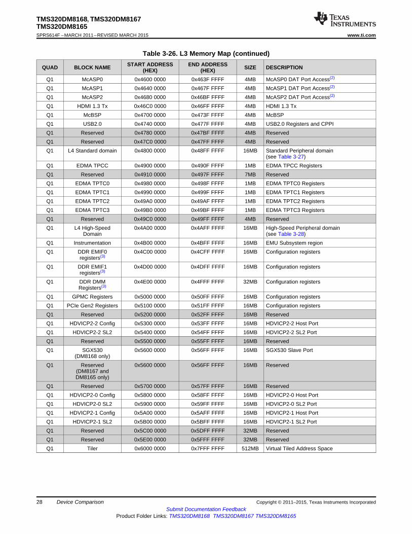
Table 3-26 shows the general device level-3 (L3) memory map. The table represents the physicaladdresses used by the L3 infrastructure. Some processors within the device (such as Cortex™-A8 ARM,C674x DSP) may re-map these targets to different virtual addresses through an internal or external MMU.Processors without MMUs and other bus masters use these physical addresses to access L3 regions.Note that not all masters have access to all L3 regions, but only those with defined connectivity, as shownin Table 7-1. For a list of the specific peripherals attached to each of the Level-4 (L4) peripheral ports seeSection 7.2. The L3 interconnect returns an address-hole error if any initiator attempts to access a targetto which it has no connection.
Table 3-26. L3 Memory Map
START ADDRESS END ADDRESSQUAD BLOCK NAME SIZE DESCRIPTION(HEX) (HEX)Q0 GPMC 0x0100 0000 0x1FFF FFFF 496MB GPMC(1)
Q0 PCIe Gen2 0x2000 0000 0x2FFF FFFF 256MB PCIe Gen2 TargetsQ0 Reserved 0x3000 0000 0x3FFF FFFF 256MB ReservedQ1 Reserved 0x4000 0000 0x402F FFFF 3MB ReservedQ1 L3 OCMC0 0x4030 0000 0x4033 FFFF 256KB OCMC SRAMQ1 Reserved 0x4034 0000 0x403F FFFF 768KB Reserved (OCMC RAM0)Q1 L3 OCMC1 0x4040 0000 0x4043 FFFF 256KB OCMC SRAMQ1 Reserved 0x4044 0000 0x404F FFFF 768KB Reserved (OCMC RAM1)Q1 Reserved 0x4050 0000 0x407F FFFF 3MB ReservedQ1 C674x 0x4080 0000 0x4083 FFFF 256KB C674x UMAP0 (L2 RAM)Q1 Reserved 0x4084 0000 0x40DF FFFF 5888KB ReservedQ1 C674x 0x40E0 0000 0x40E0 7FFF 32KB C674x L1P Cache and RAMQ1 Reserved 0x40E0 8000 0x40EF FFFF 992KB ReservedQ1 C674x 0x40F0 0000 0x40F0 7FFF 32KB C674x L1D Cache and RAMQ1 Reserved 0x40F0 8000 0x40FF FFFF 992KB ReservedQ1 Reserved 0x4100 0000 0x41FF FFFF 16MB ReservedQ1 Reserved 0x4200 0000 0x43FF FFFF 32MB ReservedQ1 L3 CFG Regs 0x4400 0000 0x44BF FFFF 12MB L3 configuration registersQ1 Reserved 0x44C0 0000 0x45FF FFFF 20MB Reserved
Copyright © 2011–2015, Texas Instruments Incorporated Device Comparison 27Submit Documentation Feedback
Product Folder Links: TMS320DM8168 TMS320DM8167 TMS320DM8165
TMS320DM8168, TMS320DM8167TMS320DM8165SPRS614F –MARCH 2011–REVISED MARCH 2015 www.ti.com
Table 3-26. L3 Memory Map (continued)START ADDRESS END ADDRESSQUAD BLOCK NAME SIZE DESCRIPTION(HEX) (HEX)
Q1 McASP0 0x4600 0000 0x463F FFFF 4MB McASP0 DAT Port Access(2)
Q1 McASP1 0x4640 0000 0x467F FFFF 4MB McASP1 DAT Port Access(2)
Q1 McASP2 0x4680 0000 0x46BF FFFF 4MB McASP2 DAT Port Access(2)
Q1 HDMI 1.3 Tx 0x46C0 0000 0x46FF FFFF 4MB HDMI 1.3 TxQ1 McBSP 0x4700 0000 0x473F FFFF 4MB McBSPQ1 USB2.0 0x4740 0000 0x477F FFFF 4MB USB2.0 Registers and CPPIQ1 Reserved 0x4780 0000 0x47BF FFFF 4MB ReservedQ1 Reserved 0x47C0 0000 0x47FF FFFF 4MB ReservedQ1 L4 Standard domain 0x4800 0000 0x48FF FFFF 16MB Standard Peripheral domain
(see Table 3-27)Q1 EDMA TPCC 0x4900 0000 0x490F FFFF 1MB EDMA TPCC RegistersQ1 Reserved 0x4910 0000 0x497F FFFF 7MB ReservedQ1 EDMA TPTC0 0x4980 0000 0x498F FFFF 1MB EDMA TPTC0 RegistersQ1 EDMA TPTC1 0x4990 0000 0x499F FFFF 1MB EDMA TPTC1 RegistersQ1 EDMA TPTC2 0x49A0 0000 0x49AF FFFF 1MB EDMA TPTC2 RegistersQ1 EDMA TPTC3 0x49B0 0000 0x49BF FFFF 1MB EDMA TPTC3 RegistersQ1 Reserved 0x49C0 0000 0x49FF FFFF 4MB ReservedQ1 L4 High-Speed 0x4A00 0000 0x4AFF FFFF 16MB High-Speed Peripheral domain
Domain (see Table 3-28)Q1 Instrumentation 0x4B00 0000 0x4BFF FFFF 16MB EMU Subsystem regionQ1 DDR EMIF0 0x4C00 0000 0x4CFF FFFF 16MB Configuration registers
registers(3)
Q1 DDR EMIF1 0x4D00 0000 0x4DFF FFFF 16MB Configuration registersregisters(3)
Q1 DDR DMM 0x4E00 0000 0x4FFF FFFF 32MB Configuration registersRegisters(3)
Q1 GPMC Registers 0x5000 0000 0x50FF FFFF 16MB Configuration registersQ1 PCIe Gen2 Registers 0x5100 0000 0x51FF FFFF 16MB Configuration registersQ1 Reserved 0x5200 0000 0x52FF FFFF 16MB ReservedQ1 HDVICP2-2 Config 0x5300 0000 0x53FF FFFF 16MB HDVICP2-2 Host PortQ1 HDVICP2-2 SL2 0x5400 0000 0x54FF FFFF 16MB HDVICP2-2 SL2 PortQ1 Reserved 0x5500 0000 0x55FF FFFF 16MB ReservedQ1 SGX530 0x5600 0000 0x56FF FFFF 16MB SGX530 Slave Port
(DM8168 only)Q1 Reserved 0x5600 0000 0x56FF FFFF 16MB Reserved
(DM8167 andDM8165 only)
Q1 Reserved 0x5700 0000 0x57FF FFFF 16MB ReservedQ1 HDVICP2-0 Config 0x5800 0000 0x58FF FFFF 16MB HDVICP2-0 Host PortQ1 HDVICP2-0 SL2 0x5900 0000 0x59FF FFFF 16MB HDVICP2-0 SL2 PortQ1 HDVICP2-1 Config 0x5A00 0000 0x5AFF FFFF 16MB HDVICP2-1 Host PortQ1 HDVICP2-1 SL2 0x5B00 0000 0x5BFF FFFF 16MB HDVICP2-1 SL2 PortQ1 Reserved 0x5C00 0000 0x5DFF FFFF 32MB ReservedQ1 Reserved 0x5E00 0000 0x5FFF FFFF 32MB ReservedQ1 Tiler 0x6000 0000 0x7FFF FFFF 512MB Virtual Tiled Address Space
28 Device Comparison Copyright © 2011–2015, Texas Instruments IncorporatedSubmit Documentation Feedback
Product Folder Links: TMS320DM8168 TMS320DM8167 TMS320DM8165

TMS320DM8168, TMS320DM8167TMS320DM8165
www.ti.com SPRS614F –MARCH 2011–REVISED MARCH 2015
Table 3-26. L3 Memory Map (continued)START ADDRESS END ADDRESSQUAD BLOCK NAME SIZE DESCRIPTION(HEX) (HEX)
Q2 DDR EMIF0 and 0x8000 0000 0xBFFF FFFF 1GB DDREMIF1 SDRAM(4)
Q3 DDR EMIF0 and 0xC000 0000 0xFFFF FFFF 1GB DDREMIF1 SDRAM(4)
Q4-7 DDR DMM 0x1 0000 0000 0x1 FFFF FFFF 4GB DDR DMM Tiler Extended address map –Virtual Views (HDVPSS only)
(1) The first section of GPMC memory (0x0 - 0x00FF_FFFF) is reserved for BOOTROM. Accessible memory starts at location0x0100_0000.
(2) For more information about McASP registers accessed through the DAT port, see Table 9-78.(3) These accesses occur through the DDR DMM Tiler Ports. The DMM will split address ranges internally to address DDR EMIF and DDR
DMM control registers.(4) DDR EMIF0 and DDR EMIF1 addresses may be contiguous or bank interleaved depending on configuration of the DDR DMM; for more
details, see the DDR DMM documentation.
Copyright © 2011–2015, Texas Instruments Incorporated Device Comparison 29Submit Documentation Feedback
Product Folder Links: TMS320DM8168 TMS320DM8167 TMS320DM8165
TMS320DM8168, TMS320DM8167TMS320DM8165SPRS614F –MARCH 2011–REVISED MARCH 2015 www.ti.com
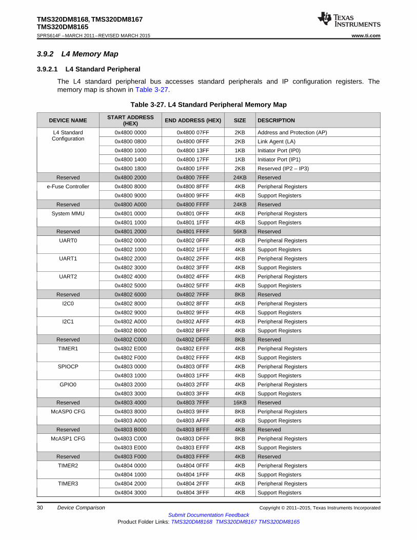
3.9.2 L4 Memory Map
3.9.2.1 L4 Standard Peripheral
The L4 standard peripheral bus accesses standard peripherals and IP configuration registers. Thememory map is shown in Table 3-27.
Table 3-27. L4 Standard Peripheral Memory Map
START ADDRESSDEVICE NAME END ADDRESS (HEX) SIZE DESCRIPTION(HEX)L4 Standard 0x4800 0000 0x4800 07FF 2KB Address and Protection (AP)Configuration 0x4800 0800 0x4800 0FFF 2KB Link Agent (LA)
0x4800 1000 0x4800 13FF 1KB Initiator Port (IP0)0x4800 1400 0x4800 17FF 1KB Initiator Port (IP1)0x4800 1800 0x4800 1FFF 2KB Reserved (IP2 – IP3)
Reserved 0x4800 2000 0x4800 7FFF 24KB Reservede-Fuse Controller 0x4800 8000 0x4800 8FFF 4KB Peripheral Registers
0x4800 9000 0x4800 9FFF 4KB Support RegistersReserved 0x4800 A000 0x4800 FFFF 24KB Reserved
System MMU 0x4801 0000 0x4801 0FFF 4KB Peripheral Registers0x4801 1000 0x4801 1FFF 4KB Support Registers
Reserved 0x4801 2000 0x4801 FFFF 56KB ReservedUART0 0x4802 0000 0x4802 0FFF 4KB Peripheral Registers
0x4802 1000 0x4802 1FFF 4KB Support RegistersUART1 0x4802 2000 0x4802 2FFF 4KB Peripheral Registers
0x4802 3000 0x4802 3FFF 4KB Support RegistersUART2 0x4802 4000 0x4802 4FFF 4KB Peripheral Registers
0x4802 5000 0x4802 5FFF 4KB Support RegistersReserved 0x4802 6000 0x4802 7FFF 8KB Reserved
I2C0 0x4802 8000 0x4802 8FFF 4KB Peripheral Registers0x4802 9000 0x4802 9FFF 4KB Support Registers
I2C1 0x4802 A000 0x4802 AFFF 4KB Peripheral Registers0x4802 B000 0x4802 BFFF 4KB Support Registers
Reserved 0x4802 C000 0x4802 DFFF 8KB ReservedTIMER1 0x4802 E000 0x4802 EFFF 4KB Peripheral Registers
0x4802 F000 0x4802 FFFF 4KB Support RegistersSPIOCP 0x4803 0000 0x4803 0FFF 4KB Peripheral Registers
0x4803 1000 0x4803 1FFF 4KB Support RegistersGPIO0 0x4803 2000 0x4803 2FFF 4KB Peripheral Registers
0x4803 3000 0x4803 3FFF 4KB Support RegistersReserved 0x4803 4000 0x4803 7FFF 16KB Reserved
McASP0 CFG 0x4803 8000 0x4803 9FFF 8KB Peripheral Registers0x4803 A000 0x4803 AFFF 4KB Support Registers
Reserved 0x4803 B000 0x4803 BFFF 4KB ReservedMcASP1 CFG 0x4803 C000 0x4803 DFFF 8KB Peripheral Registers
0x4803 E000 0x4803 EFFF 4KB Support RegistersReserved 0x4803 F000 0x4803 FFFF 4KB ReservedTIMER2 0x4804 0000 0x4804 0FFF 4KB Peripheral Registers
0x4804 1000 0x4804 1FFF 4KB Support RegistersTIMER3 0x4804 2000 0x4804 2FFF 4KB Peripheral Registers
0x4804 3000 0x4804 3FFF 4KB Support Registers
30 Device Comparison Copyright © 2011–2015, Texas Instruments IncorporatedSubmit Documentation Feedback
Product Folder Links: TMS320DM8168 TMS320DM8167 TMS320DM8165
TMS320DM8168, TMS320DM8167TMS320DM8165
www.ti.com SPRS614F –MARCH 2011–REVISED MARCH 2015
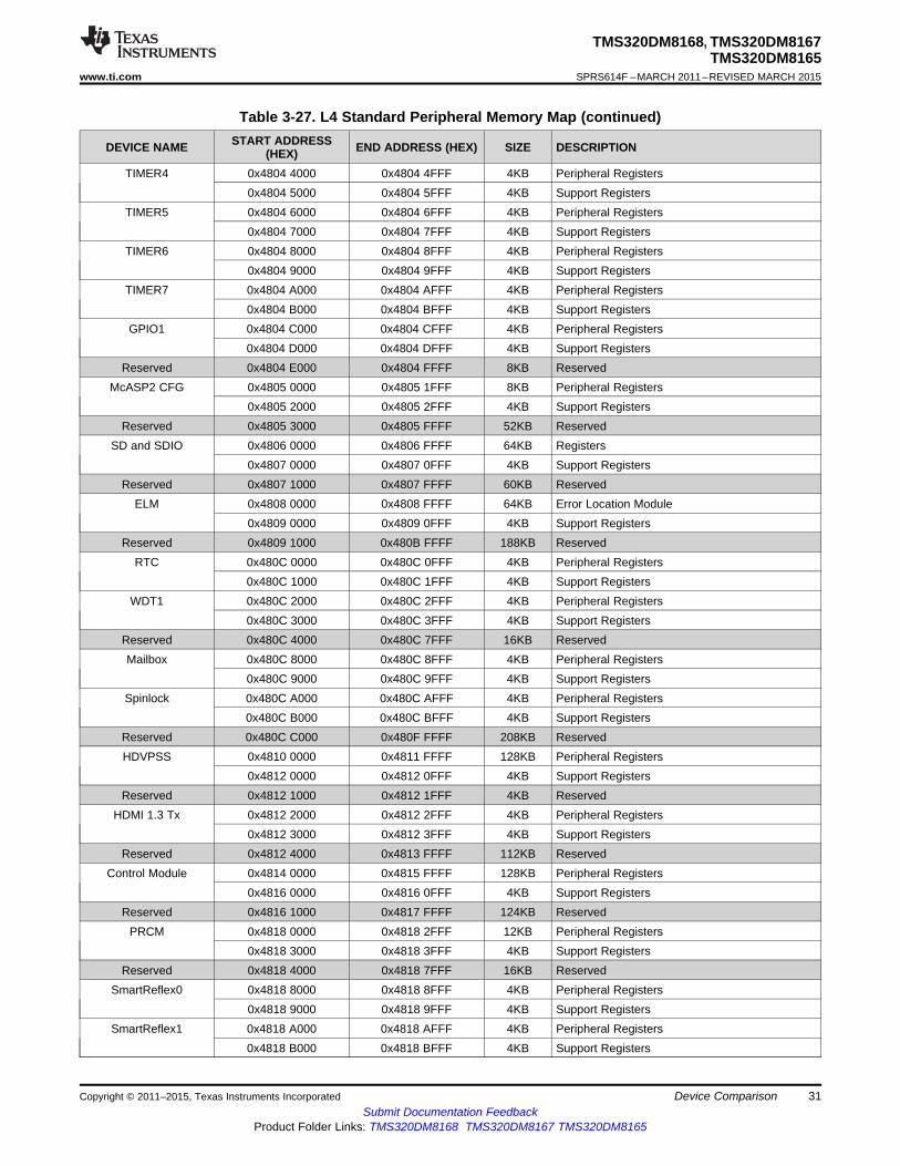
Table 3-27. L4 Standard Peripheral Memory Map (continued)START ADDRESSDEVICE NAME END ADDRESS (HEX) SIZE DESCRIPTION(HEX)
TIMER4 0x4804 4000 0x4804 4FFF 4KB Peripheral Registers0x4804 5000 0x4804 5FFF 4KB Support Registers
TIMER5 0x4804 6000 0x4804 6FFF 4KB Peripheral Registers0x4804 7000 0x4804 7FFF 4KB Support Registers
TIMER6 0x4804 8000 0x4804 8FFF 4KB Peripheral Registers0x4804 9000 0x4804 9FFF 4KB Support Registers
TIMER7 0x4804 A000 0x4804 AFFF 4KB Peripheral Registers0x4804 B000 0x4804 BFFF 4KB Support Registers
GPIO1 0x4804 C000 0x4804 CFFF 4KB Peripheral Registers0x4804 D000 0x4804 DFFF 4KB Support Registers
Reserved 0x4804 E000 0x4804 FFFF 8KB ReservedMcASP2 CFG 0x4805 0000 0x4805 1FFF 8KB Peripheral Registers
0x4805 2000 0x4805 2FFF 4KB Support RegistersReserved 0x4805 3000 0x4805 FFFF 52KB Reserved
SD and SDIO 0x4806 0000 0x4806 FFFF 64KB Registers0x4807 0000 0x4807 0FFF 4KB Support Registers
Reserved 0x4807 1000 0x4807 FFFF 60KB ReservedELM 0x4808 0000 0x4808 FFFF 64KB Error Location Module
0x4809 0000 0x4809 0FFF 4KB Support RegistersReserved 0x4809 1000 0x480B FFFF 188KB Reserved
RTC 0x480C 0000 0x480C 0FFF 4KB Peripheral Registers0x480C 1000 0x480C 1FFF 4KB Support Registers
WDT1 0x480C 2000 0x480C 2FFF 4KB Peripheral Registers0x480C 3000 0x480C 3FFF 4KB Support Registers
Reserved 0x480C 4000 0x480C 7FFF 16KB ReservedMailbox 0x480C 8000 0x480C 8FFF 4KB Peripheral Registers
0x480C 9000 0x480C 9FFF 4KB Support RegistersSpinlock 0x480C A000 0x480C AFFF 4KB Peripheral Registers
0x480C B000 0x480C BFFF 4KB Support RegistersReserved 0x480C C000 0x480F FFFF 208KB ReservedHDVPSS 0x4810 0000 0x4811 FFFF 128KB Peripheral Registers
0x4812 0000 0x4812 0FFF 4KB Support RegistersReserved 0x4812 1000 0x4812 1FFF 4KB Reserved
HDMI 1.3 Tx 0x4812 2000 0x4812 2FFF 4KB Peripheral Registers0x4812 3000 0x4812 3FFF 4KB Support Registers
Reserved 0x4812 4000 0x4813 FFFF 112KB ReservedControl Module 0x4814 0000 0x4815 FFFF 128KB Peripheral Registers
0x4816 0000 0x4816 0FFF 4KB Support RegistersReserved 0x4816 1000 0x4817 FFFF 124KB Reserved
PRCM 0x4818 0000 0x4818 2FFF 12KB Peripheral Registers0x4818 3000 0x4818 3FFF 4KB Support Registers
Reserved 0x4818 4000 0x4818 7FFF 16KB ReservedSmartReflex0 0x4818 8000 0x4818 8FFF 4KB Peripheral Registers
0x4818 9000 0x4818 9FFF 4KB Support RegistersSmartReflex1 0x4818 A000 0x4818 AFFF 4KB Peripheral Registers
0x4818 B000 0x4818 BFFF 4KB Support Registers
Copyright © 2011–2015, Texas Instruments Incorporated Device Comparison 31Submit Documentation Feedback
Product Folder Links: TMS320DM8168 TMS320DM8167 TMS320DM8165

TMS320DM8168, TMS320DM8167TMS320DM8165SPRS614F –MARCH 2011–REVISED MARCH 2015 www.ti.com
Table 3-27. L4 Standard Peripheral Memory Map (continued)START ADDRESSDEVICE NAME END ADDRESS (HEX) SIZE DESCRIPTION(HEX)
OCP Watchpoint 0x4818 C000 0x4818 CFFF 4KB Peripheral Registers0x4818 D000 0x4818 DFFF 4KB Support Registers
Reserved 0x4818 E000 0x4818 EFFF 4KB Reserved0x4818 F000 0x4818 FFFF 4KB Reserved
Reserved 0x4819 0000 0x4819 0FFF 4KB Reserved0x4819 1000 0x4819 1FFF 4KB Reserved
Reserved 0x4819 2000 0x4819 2FFF 4KB Reserved0x4819 3000 0x4819 3FFF 4KB Reserved
Reserved 0x4819 4000 0x4819 4FFF 4KB Reserved0x4819 5000 0x4819 5FFF 4KB Reserved
Reserved 0x4819 6000 0x4819 6FFF 4KB Reserved0x4819 7000 0x4819 7FFF 4KB Reserved
DDR0 Phy Ctrl Regs 0x4819 8000 0x4819 8FFF 4KB Peripheral Registers0x4819 9000 0x4819 9FFF 4KB Support Registers
DDR1 Phy Ctrl Regs 0x4819 A000 0x4819 AFFF 4KB Peripheral Registers0x4819 B000 0x4819 BFFF 4KB Support Registers
Reserved 0x4819 C000 0x481F FFFF 400KB ReservedInterrupt controller (1) 0x4820 0000 0x4820 0FFF 4KB Cortex™-A8 Accessible Only
Reserved (1) 0x4820 1000 0x4823 FFFF 252KB Cortex™-A8 Accessible OnlyMPUSS config 0x4824 0000 0x4824 0FFF 4KB Cortex™-A8 Accessible Only
register (1)
Reserved (1) 0x4824 1000 0x4827 FFFF 252KB Cortex™-A8 Accessible OnlyReserved (1) 0x4828 1000 0x482F FFFF 508KB Cortex™-A8 Accessible OnlyReserved 0x4830 0000 0x48FF FFFF 13MB Reserved
(1) These regions are decoded internally by the Cortex™-A8 Subsystem and are not physically part of the L4 standard. They are includedhere only for reference when considering the Cortex™-A8 memory map. For masters other than the Cortex™-A8, these regions arereserved.
32 Device Comparison Copyright © 2011–2015, Texas Instruments IncorporatedSubmit Documentation Feedback
Product Folder Links: TMS320DM8168 TMS320DM8167 TMS320DM8165

TMS320DM8168, TMS320DM8167TMS320DM8165
www.ti.com SPRS614F –MARCH 2011–REVISED MARCH 2015
3.9.2.2 L4 High-Speed Peripheral
The L4 high-speed peripheral bus accesses the IP configuration registers of high-speed peripherals in L3.The memory map is shown in Table 3-28.
Table 3-28. L4 High-Speed Peripheral Memory Map
START ADDRESSDEVICE NAME END ADDRESS (HEX) SIZE DESCRIPTION(HEX)L4 High Speed 0x4A00 0000 0x4A00 07FF 2KB Address and Protection (AP)configuration 0x4A00 0800 0x4A00 0FFF 2KB Link Agent (LA)
0x4A00 1000 0x4A00 13FF 1KB Initiator Port (IP0)0x4A00 1400 0x4A00 17FF 1KB Initiator Port (IP1)0x4A00 1800 0x4A00 1FFF 2KB Reserved (IP2 – IP3)
Reserved 0x4A00 2000 0x4A07 FFFF 504KB ReservedReserved 0x4A08 0000 0x4A0A 0FFF 132KB ReservedReserved 0x4A0A 1000 0x4A0F FFFF 380KB ReservedEMAC0 0x4A10 0000 0x4A10 3FFF 16KB Peripheral Registers
0x4A10 4000 0x4A10 4FFF 4KB Support RegistersReserved 0x4A10 5000 0x4A11 FFFF 108KB ReservedEMAC1 0x4A12 0000 0x4A12 3FFF 16KB Peripheral Registers
0x4A12 4000 0x4A12 4FFF 4KB Support RegistersReserved 0x4A12 5000 0x4A13 FFFF 108KB Reserved
SATA 0x4A14 0000 0x4A14 FFFF 64KB Peripheral Registers0x4A15 0000 0x4A15 0FFF 4KB Support Registers
Reserved 0x4A15 1000 0x4A17 FFFF 188KB ReservedReserved 0x4A18 0000 0x4A19 FFFF 128KB Reserved
0x4A1A 0000 0x4A1A 0FFF 4KB ReservedReserved 0x4A1A 1000 0x4AFF FFFF 14716KB Reserved
Copyright © 2011–2015, Texas Instruments Incorporated Device Comparison 33Submit Documentation Feedback
Product Folder Links: TMS320DM8168 TMS320DM8167 TMS320DM8165

TMS320DM8168, TMS320DM8167TMS320DM8165SPRS614F –MARCH 2011–REVISED MARCH 2015 www.ti.com
3.9.3 TILER Extended Addressing MapThe Tiling and Isometric Lightweight Engines for Rotation (TILER) ports are mainly used for optimized 2-Dblock accesses. The TILER also supports rotation of the image buffer at 0º, 90º, 180º, and 270º, withvertical and horizontal mirroring.
The TILER includes an additional 4-GB addressing range to access the frame buffer in these rotated andmirrored views. This range requires a thirty-third bit of address and is only accessible to peripherals thatrequire access to the multiple views. On the device, this is limited to the HD Video Processing Subsystem(HDVPSS). (Other peripherals, based on ConnID, may access any one single view through the 512-MBTILER window region located in the base 4-GB range.)
The HDVPSS may use the virtual address space of 4GB (0x1:0000:0000 – 0x1:FFFF:FFFF) since variousVPDMA clients of the HDVPSS may need to simultaneously access multiple 2-D images with differentorientations of the image buffers.
The top 4-GB address space is divided into eight sections of 512MB each. These eight sectionscorrespond to the eight different orientations as shown in Table 3-29.
Table 3-29. TILER Extended Address Memory Map
START ADDRESSBLOCK NAME END ADDRESS (HEX) SIZE DESCRIPTION(HEX)Tiler View 0 0x1 0000 0000 0x1 1FFF FFFF 512MB Natural 0° ViewTiler View 1 0x1 2000 0000 0x1 3FFF FFFF 512MB 0° with Vertical Mirror ViewTiler View 2 0x1 4000 0000 0x1 5FFF FFFF 512MB 0° with Horizontal Mirror ViewTiler View 3 0x1 6000 0000 0x1 7FFF FFFF 512MB 180° ViewTiler View 4 0x1 8000 0000 0x1 9FFF FFFF 512MB 90° with Vertical Mirror ViewTiler View 5 0x1 A000 0000 0x1 BFFF FFFF 512MB 270° ViewTiler View 6 0x1 C000 0000 0x1 DFFF FFFF 512MB 90° ViewTiler View 7 0x1 E000 0000 0x1 FFFF FFFF 512MB 90° with Horizontal Mirror View
34 Device Comparison Copyright © 2011–2015, Texas Instruments IncorporatedSubmit Documentation Feedback
Product Folder Links: TMS320DM8168 TMS320DM8167 TMS320DM8165
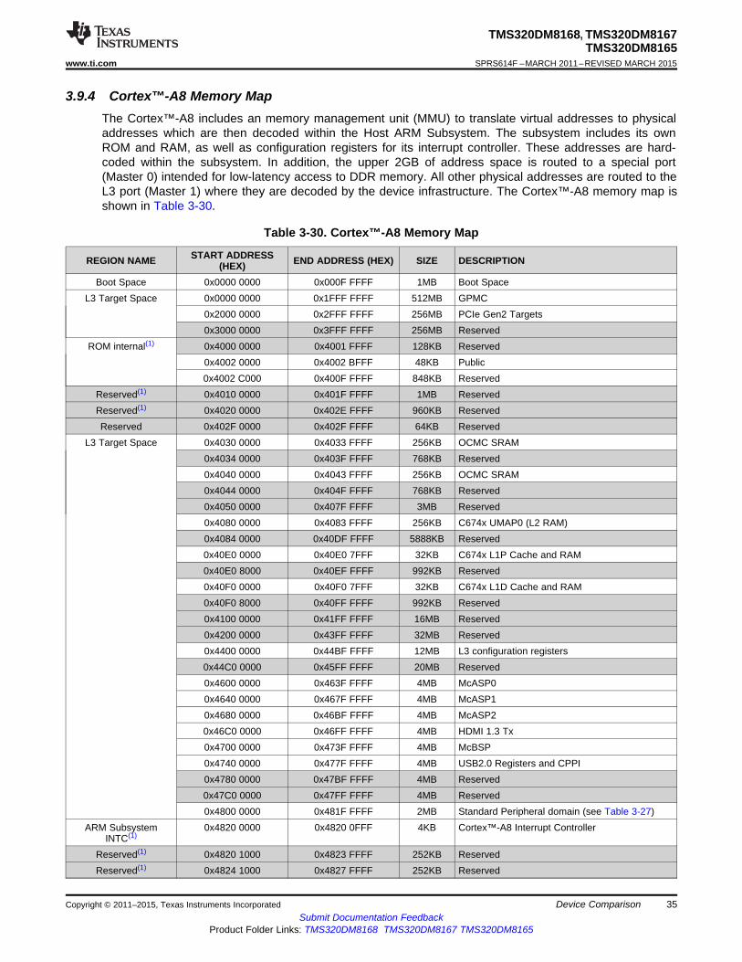
TMS320DM8168, TMS320DM8167TMS320DM8165
www.ti.com SPRS614F –MARCH 2011–REVISED MARCH 2015
3.9.4 Cortex™-A8 Memory MapThe Cortex™-A8 includes an memory management unit (MMU) to translate virtual addresses to physicaladdresses which are then decoded within the Host ARM Subsystem. The subsystem includes its ownROM and RAM, as well as configuration registers for its interrupt controller. These addresses are hard-coded within the subsystem. In addition, the upper 2GB of address space is routed to a special port(Master 0) intended for low-latency access to DDR memory. All other physical addresses are routed to theL3 port (Master 1) where they are decoded by the device infrastructure. The Cortex™-A8 memory map isshown in Table 3-30.
Table 3-30. Cortex™-A8 Memory Map
START ADDRESSREGION NAME END ADDRESS (HEX) SIZE DESCRIPTION(HEX)Boot Space 0x0000 0000 0x000F FFFF 1MB Boot Space
L3 Target Space 0x0000 0000 0x1FFF FFFF 512MB GPMC0x2000 0000 0x2FFF FFFF 256MB PCIe Gen2 Targets0x3000 0000 0x3FFF FFFF 256MB Reserved
ROM internal(1) 0x4000 0000 0x4001 FFFF 128KB Reserved0x4002 0000 0x4002 BFFF 48KB Public0x4002 C000 0x400F FFFF 848KB Reserved
Reserved(1) 0x4010 0000 0x401F FFFF 1MB ReservedReserved(1) 0x4020 0000 0x402E FFFF 960KB ReservedReserved 0x402F 0000 0x402F FFFF 64KB Reserved
L3 Target Space 0x4030 0000 0x4033 FFFF 256KB OCMC SRAM0x4034 0000 0x403F FFFF 768KB Reserved0x4040 0000 0x4043 FFFF 256KB OCMC SRAM0x4044 0000 0x404F FFFF 768KB Reserved0x4050 0000 0x407F FFFF 3MB Reserved0x4080 0000 0x4083 FFFF 256KB C674x UMAP0 (L2 RAM)0x4084 0000 0x40DF FFFF 5888KB Reserved0x40E0 0000 0x40E0 7FFF 32KB C674x L1P Cache and RAM0x40E0 8000 0x40EF FFFF 992KB Reserved0x40F0 0000 0x40F0 7FFF 32KB C674x L1D Cache and RAM0x40F0 8000 0x40FF FFFF 992KB Reserved0x4100 0000 0x41FF FFFF 16MB Reserved0x4200 0000 0x43FF FFFF 32MB Reserved0x4400 0000 0x44BF FFFF 12MB L3 configuration registers0x44C0 0000 0x45FF FFFF 20MB Reserved0x4600 0000 0x463F FFFF 4MB McASP00x4640 0000 0x467F FFFF 4MB McASP10x4680 0000 0x46BF FFFF 4MB McASP20x46C0 0000 0x46FF FFFF 4MB HDMI 1.3 Tx0x4700 0000 0x473F FFFF 4MB McBSP0x4740 0000 0x477F FFFF 4MB USB2.0 Registers and CPPI0x4780 0000 0x47BF FFFF 4MB Reserved0x47C0 0000 0x47FF FFFF 4MB Reserved0x4800 0000 0x481F FFFF 2MB Standard Peripheral domain (see Table 3-27)
ARM Subsystem 0x4820 0000 0x4820 0FFF 4KB Cortex™-A8 Interrupt ControllerINTC(1)
Reserved(1) 0x4820 1000 0x4823 FFFF 252KB ReservedReserved(1) 0x4824 1000 0x4827 FFFF 252KB Reserved
Copyright © 2011–2015, Texas Instruments Incorporated Device Comparison 35Submit Documentation Feedback
Product Folder Links: TMS320DM8168 TMS320DM8167 TMS320DM8165
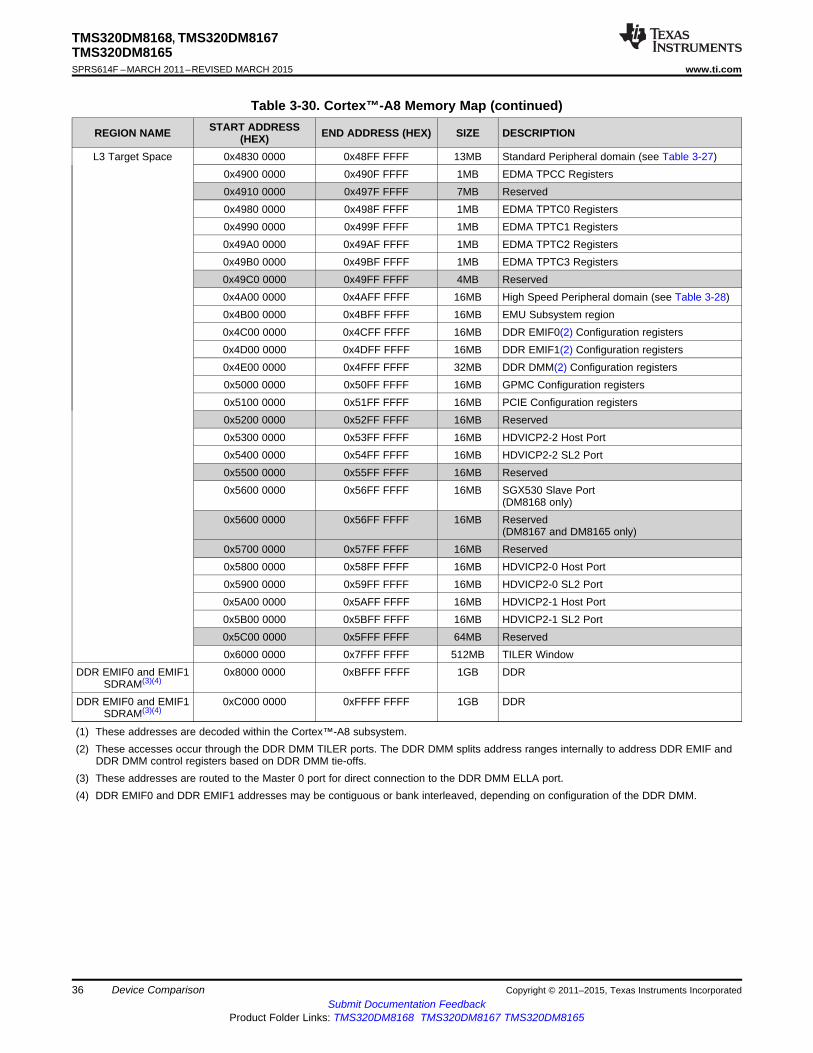
TMS320DM8168, TMS320DM8167TMS320DM8165SPRS614F –MARCH 2011–REVISED MARCH 2015 www.ti.com
Table 3-30. Cortex™-A8 Memory Map (continued)START ADDRESSREGION NAME END ADDRESS (HEX) SIZE DESCRIPTION(HEX)
L3 Target Space 0x4830 0000 0x48FF FFFF 13MB Standard Peripheral domain (see Table 3-27)0x4900 0000 0x490F FFFF 1MB EDMA TPCC Registers0x4910 0000 0x497F FFFF 7MB Reserved0x4980 0000 0x498F FFFF 1MB EDMA TPTC0 Registers0x4990 0000 0x499F FFFF 1MB EDMA TPTC1 Registers0x49A0 0000 0x49AF FFFF 1MB EDMA TPTC2 Registers0x49B0 0000 0x49BF FFFF 1MB EDMA TPTC3 Registers0x49C0 0000 0x49FF FFFF 4MB Reserved0x4A00 0000 0x4AFF FFFF 16MB High Speed Peripheral domain (see Table 3-28)0x4B00 0000 0x4BFF FFFF 16MB EMU Subsystem region0x4C00 0000 0x4CFF FFFF 16MB DDR EMIF0(2) Configuration registers0x4D00 0000 0x4DFF FFFF 16MB DDR EMIF1(2) Configuration registers0x4E00 0000 0x4FFF FFFF 32MB DDR DMM(2) Configuration registers0x5000 0000 0x50FF FFFF 16MB GPMC Configuration registers0x5100 0000 0x51FF FFFF 16MB PCIE Configuration registers0x5200 0000 0x52FF FFFF 16MB Reserved0x5300 0000 0x53FF FFFF 16MB HDVICP2-2 Host Port0x5400 0000 0x54FF FFFF 16MB HDVICP2-2 SL2 Port0x5500 0000 0x55FF FFFF 16MB Reserved0x5600 0000 0x56FF FFFF 16MB SGX530 Slave Port
(DM8168 only)0x5600 0000 0x56FF FFFF 16MB Reserved
(DM8167 and DM8165 only)0x5700 0000 0x57FF FFFF 16MB Reserved0x5800 0000 0x58FF FFFF 16MB HDVICP2-0 Host Port0x5900 0000 0x59FF FFFF 16MB HDVICP2-0 SL2 Port0x5A00 0000 0x5AFF FFFF 16MB HDVICP2-1 Host Port0x5B00 0000 0x5BFF FFFF 16MB HDVICP2-1 SL2 Port0x5C00 0000 0x5FFF FFFF 64MB Reserved0x6000 0000 0x7FFF FFFF 512MB TILER Window
DDR EMIF0 and EMIF1 0x8000 0000 0xBFFF FFFF 1GB DDRSDRAM(3)(4)
DDR EMIF0 and EMIF1 0xC000 0000 0xFFFF FFFF 1GB DDRSDRAM(3)(4)
(1) These addresses are decoded within the Cortex™-A8 subsystem.(2) These accesses occur through the DDR DMM TILER ports. The DDR DMM splits address ranges internally to address DDR EMIF and
DDR DMM control registers based on DDR DMM tie-offs.(3) These addresses are routed to the Master 0 port for direct connection to the DDR DMM ELLA port.(4) DDR EMIF0 and DDR EMIF1 addresses may be contiguous or bank interleaved, depending on configuration of the DDR DMM.
36 Device Comparison Copyright © 2011–2015, Texas Instruments IncorporatedSubmit Documentation Feedback
Product Folder Links: TMS320DM8168 TMS320DM8167 TMS320DM8165

TMS320DM8168, TMS320DM8167TMS320DM8165
www.ti.com SPRS614F –MARCH 2011–REVISED MARCH 2015
3.9.5 C674x Memory MapBecause the C674x DSP has specific hardwired address decoding built in, the C674x memory map isslightly different than that of the Cortex™-A8. The C674x has a separate CFG bus which is used toaccess L4 peripherals and its UMAP1 bus has a direct connection into HDVICP2 SL2 (HDVICP2-0 andHDVICP2-1 only) memories. All C674x MDMA port accesses are routed through the System MMU foraddress translation.
Table 3-31. C674x Memory Map
START ADDRESSREGION NAME END ADDRESS (HEX) SIZE DESCRIPTION(HEX)Reserved (1) 0x0000 0000 0x003F FFFF 4MB ReservedUMAP1 (1) 0x0040 0000 0x0043 FFFF 256KB C674x UMAP1 (HDVICP2-0 SL2)
Reserved (UMAP1) (1) 0x0044 0000 0x004F FFFF 768KB ReservedUMAP1 (1) 0x0050 0000 0x0053 FFFF 256KB C674x UMAP1 (HDVICP2-1 SL2)
Reserved (UMAP1) (1) 0x0054 0000 0x005F FFFF 768KB ReservedReserved (1) 0x0060 0000 0x007F FFFF 2MB ReservedL2 SRAM (1) 0x0080 0000 0x0083 FFFF 256KB C674x UMAP0 (L2 RAM)Reserved (1) 0x0084 0000 0x00DF FFFF 5888KB Reserved
L1P SRAM (1) 0x00E0 0000 0x00E0 7FFF 32KB C674x L1P Cache and RAMReserved (1) 0x00E0 8000 0x00EF FFFF 992KB Reserved
L1D SRAM (1) 0x00F0 0000 0x00F0 7FFF 32KB C674x L1D Cache and RAMReserved (1) 0x00F0 8000 0x017F FFFF 9184KB Reserved
Internal CFG (2) (3) 0x0180 0000 0x01BF FFFF 4MB C674x Internal CFG registersReserved (3) 0x01C0 0000 0x07FF FFFF 100MB Reserved
L4 Standard Domain (3) 0x0800 0000 0x08FF FFFF 16MB Peripheral Domain (see Table 3-27)EDMA TPCC (3) 0x0900 0000 0x090F FFFF 1MB EDMA TPCC Registers
Reserved (3) 0x0910 0000 0x097F FFFF 7MB ReservedEDMA TPTC0 (3) 0x0980 0000 0x098F FFFF 1MB EDMA TPTC0 RegistersEDMA TPTC1 (3) 0x0990 0000 0x099F FFFF 1MB EDMA TPTC1 RegistersEDMA TPTC2 (3) 0x09A0 0000 0x09AF FFFF 1MB EDMA TPTC2 RegistersEDMA TPTC3 (3) 0x09B0 0000 0x09BF FFFF 1MB EDMA TPTC3 Registers
Reserved (3) 0x09C0 0000 0x09FF FFFF 4MB ReservedL4 High-Speed 0x0A00 0000 0x0AFF FFFF 16MB Peripheral Domain (see Table 3-28)
Domain (3)
Reserved (3) 0x0B00 0000 0x0FFF FFFF 80MB ReservedC674x L1 and L2 (4) 0x1000 0000 0x10FF FFFF 16MB C674x Internal Global Address
MDMA L3 (5) 0x1100 0000 0xFFFF FFFF 3824MB System MMU Mapped L3 Regions
(1) Addresses 0x0000 0000 to 0x017F FFFF are internal to the C674x device.(2) Addresses 0x0180 0000 to 0x01BF FFFF are reserved for C674x internal CFG registers.(3) Addresses 0x01C0 0000 to 0x0FFF FFFF are mapped to the C674x CFG bus.(4) Addresses 0x1000 0000 to 0x10FF FFFF are mapped to C674x internal addresses 0x0000 0000 to 0x00FF FFFF.(5) These accesses are routed through the System MMU where the page tables translate to the physical L3 addresses shown in Table 3-
26.
Copyright © 2011–2015, Texas Instruments Incorporated Device Comparison 37Submit Documentation Feedback
Product Folder Links: TMS320DM8168 TMS320DM8167 TMS320DM8165
TMS320DM8168, TMS320DM8167TMS320DM8165SPRS614F –MARCH 2011–REVISED MARCH 2015 www.ti.com
4 Terminal Configuration and Functions
4.1 Pin AssignmentsExtensive use of pin multiplexing is used to accommodate the largest number of peripheral functions inthe smallest possible package. Pin multiplexing is controlled using a combination of hardwareconfiguration at device reset and software programmable register settings. For more information on pinmuxing, see Section 6.5, Pin Multiplexing Control.
4.1.1 Pin Map (Bottom View)Figure 4-1 through Figure 4-19 show the bottom view of the package pin assignments in 15 sections (A,B, C, D, E, F, G, H, I, J, K, L, M, N, and O).
NOTEPin map sections D, E, K, and L show the different pin names for silicon revision 1.x devicesand silicon revision 2.x devices.
38 Terminal Configuration and Functions Copyright © 2011–2015, Texas Instruments IncorporatedSubmit Documentation Feedback
Product Folder Links: TMS320DM8168 TMS320DM8167 TMS320DM8165
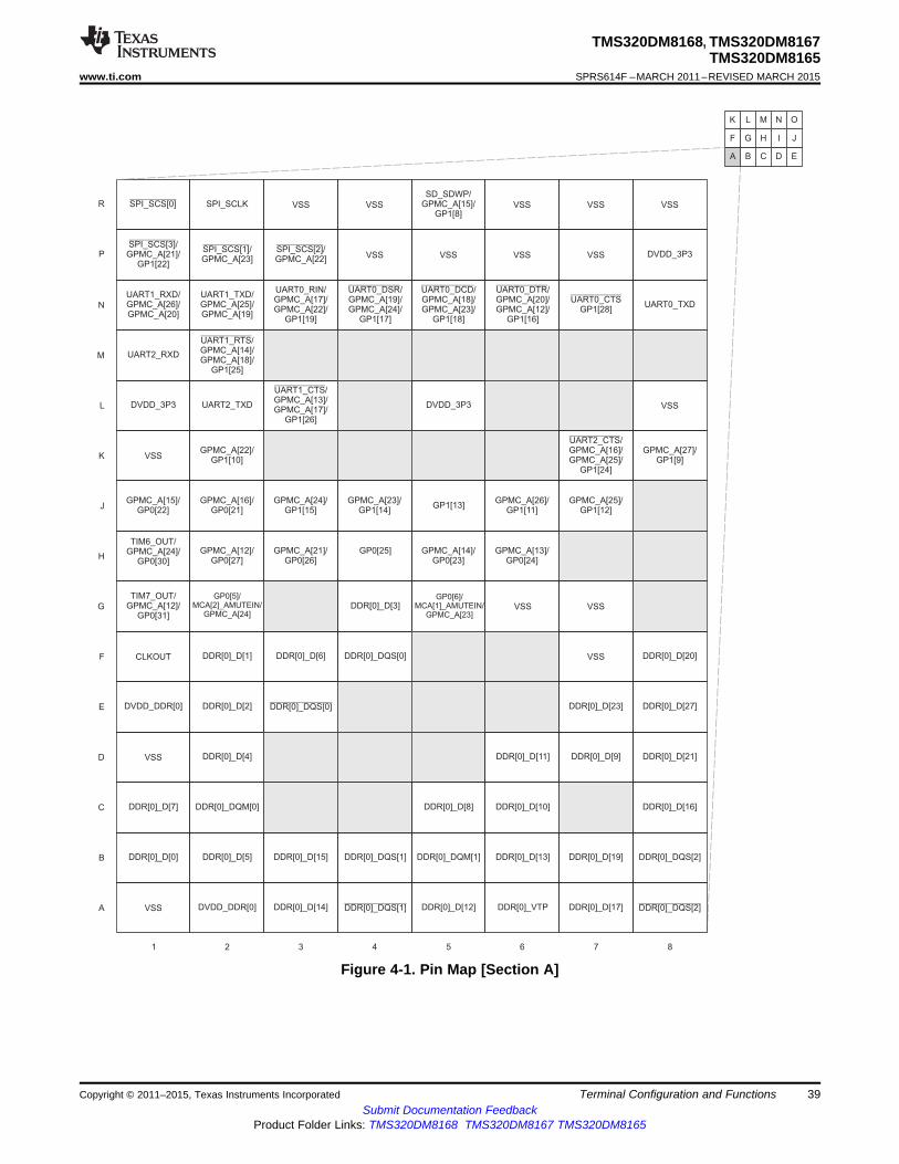
SPI_SCS[0] SPI_SCLK VSS VSS
SD_SDWP/GPMC_A[15]/
GP1[8]VSS VSS VSS
SPI_SCS[3]/GPMC_A[21]/
GP1[22]
SPI_SCS[1]/GPMC_A[23]
SPI_SCS[2]/GPMC_A[22]
VSS VSS VSS VSS DVDD_3P3
UART1_RXD/GPMC_A[26]/GPMC_A[20]
UART1_TXD/GPMC_A[25]/GPMC_A[19]
UART0_RIN/GPMC_A[17]/GPMC_A[22]/
GP1[19]
UART0_DSR/GPMC_A[19]/GPMC_A[24]/
GP1[17]
UART0_DCD/GPMC_A[18]/GPMC_A[23]/
GP1[18]
UART0_DTR/GPMC_A[20]/GPMC_A[12]/
GP1[16]
UART0_CTSGP1[28]
UART0_TXD
R
P
N
M
L
K
J
H
G
F
E
1 2 3 4 5 6 7 8
A B C
UART2_RXD
UART1_RTS/GPMC_A[14]/GPMC_A[18]/
GP1[25]
DVDD_3P3 UART2_TXD
UART1_CTS/GPMC_A[13]/GPMC_A[17]/
GP1[26]
DVDD_3P3 VSS
D
C
B
A
F G H
D
I
K L M N
E
J
O
VSSGPMC_A[22]/
GP1[10]
UART2_CTS/GPMC_A[16]/GPMC_A[25]/
GP1[24]
GPMC_A[27]/GP1[9]
GPMC_A[15]/GP0[22]
GPMC_A[16]/GP0[21]
GPMC_A[24]/GP1[15]
GPMC_A[23]/GP1[14]
GP1[13]GPMC_A[26]/
GP1[11]GPMC_A[25]/
GP1[12]
TIM6_OUT/GPMC_A[24]/
GP0[30]
GPMC_A[12]/GP0[27]
GPMC_A[21]/GP0[26]
GP0[25] GPMC_A[14]/GP0[23]
GPMC_A[13]/GP0[24]
TIM7_OUT/GPMC_A[12]/
GP0[31]
GP0[5]/MCA[2]_AMUTEIN/
GPMC_A[24]DDR[0]_D[3]
GP0[6]/MCA[1]_AMUTEIN/
GPMC_A[23]VSS VSS
CLKOUT DDR[0]_D[1] DDR[0]_D[6] DDR[0]_DQS[0] VSS DDR[0]_D[20]
DVDD_DDR[0] DDR[0]_D[2] DDR[0]_DQS[0] DDR[0]_D[23] DDR[0]_D[27]
VSS DDR[0]_D[4] DDR[0]_D[11] DDR[0]_D[9] DDR[0]_D[21]
DDR[0]_D[7] DDR[0]_DQM[0] DDR[0]_D[8] DDR[0]_D[10] DDR[0]_D[16]
DDR[0]_D[0] DDR[0]_D[5] DDR[0]_D[15] DDR[0]_DQS[1] DDR[0]_DQM[1] DDR[0]_D[13] DDR[0]_D[19] DDR[0]_DQS[2]
VSS DVDD_DDR[0] DDR[0]_D[14] DDR[0]_DQS[1] DDR[0]_D[12] DDR[0]_VTP DDR[0]_D[17] DDR[0]_DQS[2]
TMS320DM8168, TMS320DM8167TMS320DM8165
www.ti.com SPRS614F –MARCH 2011–REVISED MARCH 2015
Figure 4-1. Pin Map [Section A]
Copyright © 2011–2015, Texas Instruments Incorporated Terminal Configuration and Functions 39Submit Documentation Feedback
Product Folder Links: TMS320DM8168 TMS320DM8167 TMS320DM8165
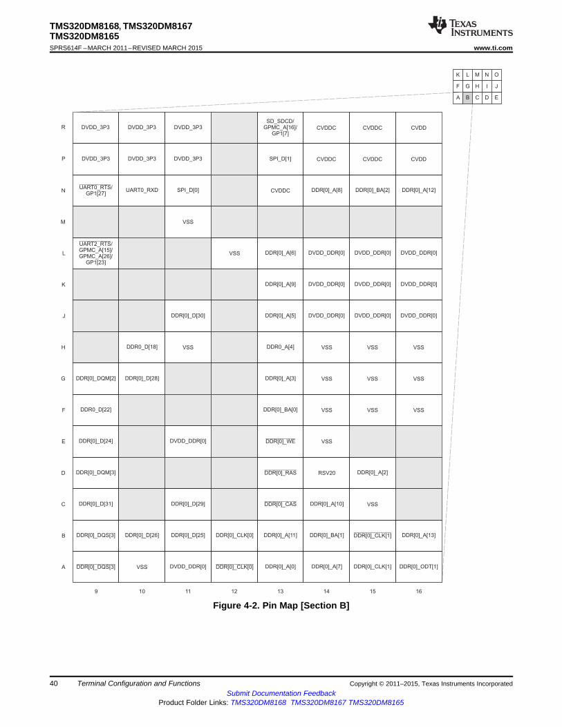
DVDD_3P3 DVDD_3P3 DVDD_3P3SD_SDCD/
GPMC_A[16]/GP1[7]
CVDDC CVDDC CVDD
DVDD_3P3 DVDD_3P3 DVDD_3P3 SPI_D[1] CVDDC CVDDC CVDD
UART0_RTS/GP1[27]
UART0_RXD SPI_D[0] CVDDC DDR[0]_A[8] DDR[0]_BA[2] DDR[0]_A[12]
9 10 11 12 13 14 15 16
A B C
VSS
UART2_RTS/GPMC_A[15]/GPMC_A[26]/
GP1[23]
VSS DDR[0]_A[6]
R
P
N
M
L
K
J
H
G
F
E
D
C
B
A
F G H
D
I
K L M N
E
J
O
DDR[0]_A[9]
DDR[0]_D[30] DDR[0]_A[5] DVDD_DDR[0]
DDR0_D[18] VSS DDR0_A[4] VSS VSS VSS
DDR[0]_DQM[2] DDR[0]_D[28] DDR[0]_A[3] VSS VSS VSS
DDR0_D[22] DDR[0]_BA[0] VSS VSS VSS
DDR[0]_D[24] DVDD_DDR[0] DDR[0]_WE VSS
DDR[0]_DQM[3] DDR[0]_RAS RSV20 DDR[0]_A[2]
DDR[0]_D[31] DDR[0]_D[29] DDR[0]_CAS DDR[0]_A[10] VSS
DDR[0]_DQS[3] DDR[0]_D[26] DDR[0]_D[25] DDR[0]_CLK[0] DDR[0]_A[11] DDR[0]_BA[1] DDR[0]_CLK[1] DDR[0]_A[13]
DDR[0]_DQS[3] VSS DVDD_DDR[0] DDR[0]_CLK[0] DDR[0]_A[0] DDR[0]_A[7] DDR[0]_CLK[1] DDR[0]_ODT[1]
DVDD_DDR[0] DVDD_DDR[0] DVDD_DDR[0]
DVDD_DDR[0] DVDD_DDR[0] DVDD_DDR[0]
DVDD_DDR[0] DVDD_DDR[0]
TMS320DM8168, TMS320DM8167TMS320DM8165SPRS614F –MARCH 2011–REVISED MARCH 2015 www.ti.com
Figure 4-2. Pin Map [Section B]
40 Terminal Configuration and Functions Copyright © 2011–2015, Texas Instruments IncorporatedSubmit Documentation Feedback
Product Folder Links: TMS320DM8168 TMS320DM8167 TMS320DM8165

R
P
N
M
L
K
J
H
G
F
E
D
C
B
A
CVDD CVDD CVDD CVDD CVDD CVDD CVDDC CVDDC
CVDD CVDD CVDD CVDD CVDD CVDD CVDDC CVDDC
DDR[0]_A[1] VSS RSV3 RSV4 DDR[1]_A[1] DDR[1]_A[12] DDR[1]_BA[2] DDR[1]_A[8]
17 18 19 20 21 22 23 24
A B C
DVDD_DDR[0] DVDD_DDR[1]
F G H
D
I
K L M N
E
J
O
VSS VSS VSS VSS VSS VSS VSS VSS
VSS VSS VSS VSS VSS VSS VSS
VSS DDR[0]_CS[1] DDR[1]_CS[1] VSS VSS VSS VSS
DDR[0]_ODT[0] DEVOSC_DVDD18 DDR[1]_ODT[0] VSS
DDR[0]_A[14] DDR[0]_RST DDR[1]_RST DDR[1]_A[14] DDR[1]_A[2] RSV8
VSS DDR[0]_CKE DEV_MXO DDR[1]_CKE VSS VSS DDR[1]_A[10]
DDR[0]_CS[0] VDDA_PLL DEVOSC_VSS VSSA_PLL DDR[1]_CS[0] DDR[1]_A[13] DDR[1]_CLK[1] DDR[1]_BA[1]
VREFSSTL_DDR[0] VDDA_PLLDEV_MXI/
DEV_CLKINVSSA_PLL VREFSSTL_DDR[1] DDR[1]_ODT[1] DDR[1]_CLK[1] DDR[1]_A[7]
DVDD_DDR[0] DVDD_DDR[0]
DVDD_DDR[0] DVDD_DDR[0]DVDD_DDR[0]
DVDD_DDR[0] DVDD_DDR[0]
DVDD_DDR[1] DVDD_DDR[1] DVDD_DDR[1] DVDD_DDR[1]
DVDD_DDR[1] DVDD_DDR[1] DVDD_DDR[1] DVDD_DDR[1] DVDD_DDR[1]
DVDD_DDR[1] DVDD_DDR[1] DVDD_DDR[1] DVDD_DDR[1] DVDD_DDR[1]DVDD_DDR[1]
TMS320DM8168, TMS320DM8167TMS320DM8165
www.ti.com SPRS614F –MARCH 2011–REVISED MARCH 2015
Figure 4-3. Pin Map [Section C]
Copyright © 2011–2015, Texas Instruments Incorporated Terminal Configuration and Functions 41Submit Documentation Feedback
Product Folder Links: TMS320DM8168 TMS320DM8167 TMS320DM8165
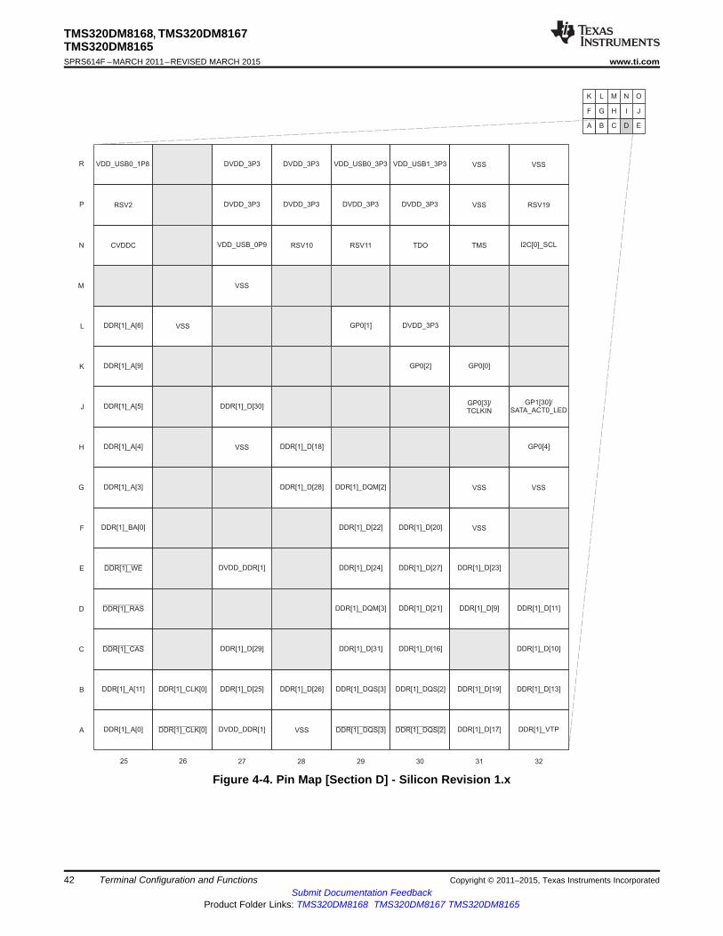
R
P
N
M
L
K
J
H
G
F
E
D
C
B
A
VDD_USB0_1P8 DVDD_3P3 DVDD_3P3 VDD_USB0_3P3 VDD_USB1_3P3 VSS VSS
RSV2 DVDD_3P3 DVDD_3P3 DVDD_3P3 DVDD_3P3 VSS RSV19
CVDDC VDD_USB_0P9 RSV10 RSV11 TDO TMS I2C[0]_SCL
25 26 27 28 29 30 31 32
A B C
VSS
DDR[1]_A[6] VSS GP0[1] DVDD_3P3
F G H
D
I
K L M N
E
J
O
DDR[1]_A[9] GP0[2] GP0[0]
DDR[1]_A[5] DDR[1]_D[30] GP0[3]/TCLKIN
GP1[30]/SATA_ACT0_LED
DDR[1]_A[4] VSS DDR[1]_D[18] GP0[4]
DDR[1]_A[3] DDR[1]_D[28] DDR[1]_DQM[2] VSS VSS
DDR[1]_BA[0] DDR[1]_D[22] DDR[1]_D[20] VSS
DDR[1]_WE DVDD_DDR[1] DDR[1]_D[24] DDR[1]_D[27] DDR[1]_D[23]
DDR[1]_RAS DDR[1]_DQM[3] DDR[1]_D[21] DDR[1]_D[9] DDR[1]_D[11]
DDR[1]_CAS DDR[1]_D[29] DDR[1]_D[31] DDR[1]_D[16] DDR[1]_D[10]
DDR[1]_A[11] DDR[1]_CLK[0] DDR[1]_D[25] DDR[1]_D[26] DDR[1]_DQS[3] DDR[1]_DQS[2] DDR[1]_D[19] DDR[1]_D[13]
DDR[1]_A[0] DDR[1]_CLK[0] DVDD_DDR[1] VSS DDR[1]_DQS[3] DDR[1]_DQS[2] DDR[1]_D[17] DDR[1]_VTP
TMS320DM8168, TMS320DM8167TMS320DM8165SPRS614F –MARCH 2011–REVISED MARCH 2015 www.ti.com
Figure 4-4. Pin Map [Section D] - Silicon Revision 1.x
42 Terminal Configuration and Functions Copyright © 2011–2015, Texas Instruments IncorporatedSubmit Documentation Feedback
Product Folder Links: TMS320DM8168 TMS320DM8167 TMS320DM8165

R
P
N
M
L
K
J
H
G
F
E
D
C
B
A
VDD_USB0_1P8 DVDD_3P3 DVDD_3P3 VDD_USB0_3P3 VDD_USB1_3P3 VSS VSS
RSV2 DVDD_3P3 DVDD_3P3 DVDD_3P3 DVDD_3P3 VSS RSV19
CVDDC VDD_USB_0P9 RSV10 RSV11 TDO TMS I2C[0]_SCL
25 26 27 28 29 30 31 32
A B C
VSS
DDR[1]_A[6] VSS GP0[1] DVDD_3P3
F G H
D
I
K L M N
E
J
O
DDR[1]_A[9] GP0[2] GP0[0]
DDR[1]_A[5] DDR[1]_D[30] GP0[3]/TCLKIN
GP1[30]/SATA_ACT1_LED
DDR[1]_A[4] VSS DDR[1]_D[18] GP0[4]
DDR[1]_A[3] DDR[1]_D[28] DDR[1]_DQM[2] VSS VSS
DDR[1]_BA[0] DDR[1]_D[22] DDR[1]_D[20] VSS
DDR[1]_WE DVDD_DDR[1] DDR[1]_D[24] DDR[1]_D[27] DDR[1]_D[23]
DDR[1]_RAS DDR[1]_DQM[3] DDR[1]_D[21] DDR[1]_D[9] DDR[1]_D[11]
DDR[1]_CAS DDR[1]_D[29] DDR[1]_D[31] DDR[1]_D[16] DDR[1]_D[10]
DDR[1]_A[11] DDR[1]_CLK[0] DDR[1]_D[25] DDR[1]_D[26] DDR[1]_DQS[3] DDR[1]_DQS[2] DDR[1]_D[19] DDR[1]_D[13]
DDR[1]_A[0] DDR[1]_CLK[0] DVDD_DDR[1] VSS DDR[1]_DQS[3] DDR[1]_DQS[2] DDR[1]_D[17] DDR[1]_VTP
TMS320DM8168, TMS320DM8167TMS320DM8165
www.ti.com SPRS614F –MARCH 2011–REVISED MARCH 2015
Figure 4-5. Pin Map [Section D] - Silicon Revision 2.x
Copyright © 2011–2015, Texas Instruments Incorporated Terminal Configuration and Functions 43Submit Documentation Feedback
Product Folder Links: TMS320DM8168 TMS320DM8167 TMS320DM8165

VSS RSV16 USB1_DRVVBUS USB1_DN USB1_DP
RSV18 RSV17 USB0_DRVVBUS USB0_DN USB0_DP
I2C[0]_SDA I2C[1]_SCL I2C[1]_SDA VDD_USB0_VBUS USB0_R1
R
P
N
M
L
K
J
H
G
F
E
33 34 35 36 37
A B C
EMU3 EMU4
VSS DVDD_3P3 EMU1 EMU2
D
C
B
A
F G H
D
I
K L M N
E
J
O
TRST VSS
GP1[31]/SATA_ACT1_LED TDI EMU0 RTCK TCLK
TIM4_OUT/GP0[28]
TIM5_OUT/GP0[29]
GP0[7]/MCA[0]_AMUTEIN
WD_OUT CLKIN32
RESET DDR[1]_D[3] NMI RSTOUT
DDR[1]_DQS[0] DDR[1]_D[6] DDR[1]_D[1] POR
DDR[1]_DQS[0] DDR[1]_D[2] VSS
DDR[1]_D[4] DVDD_DDR[1]
DDR[1]_D[8] DDR[1]_DQM[0] DDR[1]_D[7]
DDR[1]_DQM[1] DDR[1]_DQS[1] DDR[1]_D[15] DDR[1]_D[5] DDR[1]_D[0]
DDR[1]_D[12] DDR[1]_DQS[1] DDR[1]_D[14] DVDD_DDR[1] VSS
TMS320DM8168, TMS320DM8167TMS320DM8165SPRS614F –MARCH 2011–REVISED MARCH 2015 www.ti.com
Figure 4-6. Pin Map [Section E] - Silicon Revision 1.x
44 Terminal Configuration and Functions Copyright © 2011–2015, Texas Instruments IncorporatedSubmit Documentation Feedback
Product Folder Links: TMS320DM8168 TMS320DM8167 TMS320DM8165
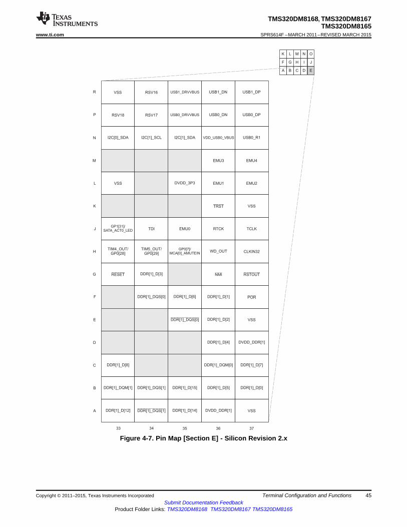
VSS RSV16 USB1_DRVVBUS USB1_DN USB1_DP
RSV18 RSV17 USB0_DRVVBUS USB0_DN USB0_DP
I2C[0]_SDA I2C[1]_SCL I2C[1]_SDA VDD_USB0_VBUS USB0_R1
R
P
N
M
L
K
J
H
G
F
E
33 34 35 36 37
A B C
EMU3 EMU4
VSS DVDD_3P3 EMU1 EMU2
D
C
B
A
F G H
D
I
K L M N
E
J
O
TRST VSS
GP1[31]/SATA_ACT0_LED TDI EMU0 RTCK TCLK
TIM4_OUT/GP0[28]
TIM5_OUT/GP0[29]
GP0[7]/MCA[0]_AMUTEIN
WD_OUT CLKIN32
RESET DDR[1]_D[3] NMI RSTOUT
DDR[1]_DQS[0] DDR[1]_D[6] DDR[1]_D[1] POR
DDR[1]_DQS[0] DDR[1]_D[2] VSS
DDR[1]_D[4] DVDD_DDR[1]
DDR[1]_D[8] DDR[1]_DQM[0] DDR[1]_D[7]
DDR[1]_DQM[1] DDR[1]_DQS[1] DDR[1]_D[15] DDR[1]_D[5] DDR[1]_D[0]
DDR[1]_D[12] DDR[1]_DQS[1] DDR[1]_D[14] DVDD_DDR[1] VSS
TMS320DM8168, TMS320DM8167TMS320DM8165
www.ti.com SPRS614F –MARCH 2011–REVISED MARCH 2015
Figure 4-7. Pin Map [Section E] - Silicon Revision 2.x
Copyright © 2011–2015, Texas Instruments Incorporated Terminal Configuration and Functions 45Submit Documentation Feedback
Product Folder Links: TMS320DM8168 TMS320DM8167 TMS320DM8165
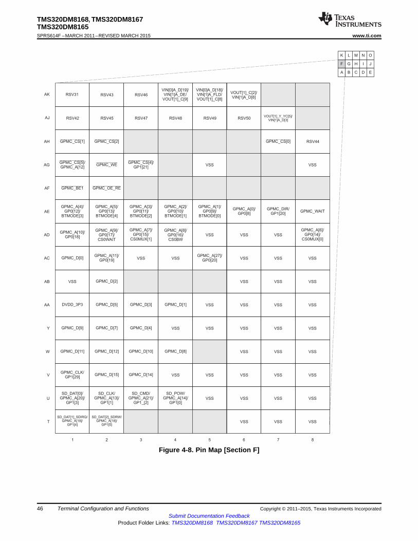
RSV31VIN[0]A_D[19]/VIN[1]A_DE/
VOUT[1]_C[9]
VIN[0]A_D[18]/VIN[1]A_FLD/VOUT[1]_C[8]
VOUT[1]_C[2]/VIN[1]A_D[8]
VOUT[1]_Y_YC[5]/VIN[1]A_D[3]
GPMC_CS[1] GPMC_CS[2] GPMC_CS[0]
AK
AJ
AH
AG
AF
AE
AD
AC
AB
AA
Y
1 2 3 4 5 6 7 8
A B C
GPMC_CS[5]/GPMC_A[12]
GPMC_WEGPMC_CS[4]/
GP1[21]VSS VSS
GPMC_BE1 GPMC_OE_RE
W
V
U
T
F G H
D
I
K L M N
E
J
O
GPMC_A[4]/GP0[12]/
BTMODE[3]
GPMC_A[5]/GP0[13]/
BTMODE[4]
GPMC_A[3]/GP0[11]/
BTMODE[2]
GPMC_A[2]/GP0[10]/
BTMODE[1]
GPMC_A[1]/GP0[9]/
BTMODE[0]
GPMC_A[0]/GP0[8]
GPMC_DIR/GP1[20]
GPMC_WAIT
GPMC_A[10]/GP0[18]
GPMC_A[9]/GP0[17]/CS0WAIT
GPMC_A[7]/GP0[15]/
CS0MUX[1]
GPMC_A[8]/GP0[16]/CS0BW
VSS VSS VSS
GPMC_A[6]/GP0[14]/
CS0MUX[0]
GPMC_D[0]GPMC_A[11]/
GP0[19]VSS VSS
GPMC_A[27]/GP0[20]
VSS VSS VSS
VSS GPMC_D[2] VSS VSS VSS
DVDD_3P3 GPMC_D[5] GPMC_D[3] GPMC_D[1] VSS VSS VSS VSS
GPMC_D[9] GPMC_D[7] GPMC_D[4] VSS VSS VSS VSS VSS
GPMC_D[11] GPMC_D[12] GPMC_D[10] GPMC_D[8] VSS VSS VSS
GPMC_CLK/GP1[29]
GPMC_D[15] GPMC_D[14] VSS VSS VSS VSS VSS
SD_DAT[0]/GPMC_A[20]/
GP1[3]
SD_CLK/GPMC_A[13]/
GP1[1]
SD_CMD/GPMC_A[21]/
GP1_[2]
SD_POW/GPMC_A[14]/
GP1[0]VSS VSS VSS VSS
SD_DAT[1]_SDIRQ/GPMC_A[19]/
GP1[4]
SD_DAT[2]_SDRW/GPMC_A[18]/
GP1[5]VSS VSS VSS
RSV42
RSV43
RSV44
RSV45
RSV46
RSV47 RSV48 RSV49 RSV50
TMS320DM8168, TMS320DM8167TMS320DM8165SPRS614F –MARCH 2011–REVISED MARCH 2015 www.ti.com
Figure 4-8. Pin Map [Section F]
46 Terminal Configuration and Functions Copyright © 2011–2015, Texas Instruments IncorporatedSubmit Documentation Feedback
Product Folder Links: TMS320DM8168 TMS320DM8167 TMS320DM8165
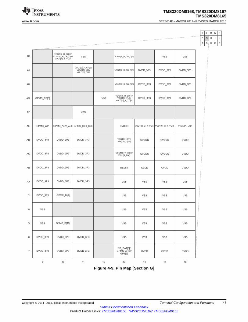
AK
AJ
AH
AG
AF
AE
AD
AC
AB
AA
Y
W
V
U
T
VOUT[0]_R_CR[8]/VOUT[0]_B_CB_C[0]/
VOUT[1]_Y_YC[8]VSS VOUT[0]_B_CB_C[5] VSS VSS
VOUT[0]_R_CR[0]/VOUT[1]_C[8]/VOUT[1]_CLK
VOUT[0]_B_CB_C[6] DVDD_3P3 DVDD_3P3 DVDD_3P3
VOUT[0]_B_CB_C[8] DVDD_3P3 DVDD_3P3 DVDD_3P3
9 10 11 12 13 14 15 16
A B C
GPMC_CS[3] VSSVOUT[0]_R_CR[4]/
VOUT[0]_FLD/VOUT[1]_Y_YC[4]
DVDD_3P3 DVDD_3P3 DVDD_3P3
VSS
F G H
D
I
K L M N
E
J
O
GPMC_WP GPMC_ _ALEADV GPMC_ _CLEBE0 CVDDC VOUT[0]_G_Y_YC[6] VOUT[0]_G_Y_YC[2] VIN[0]A_D[9]
DVDD_3P3 DVDD_3P3 DVDD_3P3 VOUT[1]_C[7]/VIN[1]A_D[13]
CVDDC CVDDC CVDD
DVDD_3P3 DVDD_3P3 DVDD_3P3 VOUT[1]_Y_YC[6]/VIN[1]A_D[4]
CVDDC CVDDC CVDD
DVDD_3P3 DVDD_3P3 DVDD_3P3 CVDD CVDD CVDD
DVDD_3P3 DVDD_3P3 DVDD_3P3 VSS VSS VSS VSS
DVDD_3P3 GPMC_D[6] VSS VSS VSS VSS
VSS VSS VSS VSS VSS
VSS GPMC_D[13] VSS VSS VSS VSS
DVDD_3P3 DVDD_3P3 DVDD_3P3 VSS VSS VSS VSS
DVDD_3P3 DVDD_3P3 DVDD_3P3SD_DAT[3]/
GPMC_A[17]/GP1[6]
CVDD CVDD CVDD
RSV51
TMS320DM8168, TMS320DM8167TMS320DM8165
www.ti.com SPRS614F –MARCH 2011–REVISED MARCH 2015
Figure 4-9. Pin Map [Section G]
Copyright © 2011–2015, Texas Instruments Incorporated Terminal Configuration and Functions 47Submit Documentation Feedback
Product Folder Links: TMS320DM8168 TMS320DM8167 TMS320DM8165

AK
AJ
AH
AG
AF
AE
AD
AC
AB
AA
Y
W
V
U
T
VSS VSS VSS VSSA_HD VSSA_HD VSS VSS
DVDD_3P3 VSS VIN[0]A_D[0] DVDD1P8 VDDA_SD_1P8 VDDA_HD_1P8 DVDD1P8
DVDD_3P3 VIN[0]A_D[2] VDAC_VREF VDDA_SD_1P8 VDDA_SD_1P8 VDDA_HD_1P8 RSV15
17 18 19 20 21 22 23 24
A B C
DVDD_3P3 VDDA_SD_1P0 VDDA_HD_1P0 RSV13
F G H
D
I
K L M N
E
J
O
VSS VSS VSS VSS VDAC_RBIAS_HD RSV7 HDMI_HPDET
CVDD CVDD CVDD CVDD CVDD CVDD CVDDC CVDDC
CVDD CVDD CVDD CVDD CVDD CVDD CVDDC CVDDC
CVDD CVDD CVDD CVDD CVDD CVDD CVDD CVDD
VSS VSS VSS VSS VSS VSS VSS VSS
VSS VSS VSS VSS VSS VSS VSS VSS
VSS VSS VSS VSS VSS VSS VSS VSS
VSS VSS VSS VSS VSS VSS VSS VSS
VSS VSS VSSA_PLL VSS VSS VSS VSS VSS
CVDD CVDD CVDD CVDD CVDD CVDD CVDD CVDD
RSV52
RSV53
RSV55
RSV54
RSV56
RSV57
TMS320DM8168, TMS320DM8167TMS320DM8165SPRS614F –MARCH 2011–REVISED MARCH 2015 www.ti.com
Figure 4-10. Pin Map [Section H]
48 Terminal Configuration and Functions Copyright © 2011–2015, Texas Instruments IncorporatedSubmit Documentation Feedback
Product Folder Links: TMS320DM8168 TMS320DM8167 TMS320DM8165

AK
AJ
AH
AG
AF
AE
AD
AC
AB
AA
Y
W
V
U
T
HDMI_SDA VSS MCA[0]_ACLKR MCA[1]_AXR[1]
VSS MCA[0]_AHCLKR MCA[0]_AFSX MCA[0]_AXR[1]
RSV14 MCA[0]_ACLKX MCA[0]_AHCLKX
25 26 27 28 29 30 31 32
A B C
RSV12 VSS EMAC[0]_TXD[4] MCA[0]_AFSR VSS
VSS
F G H
D
I
K L M N
E
J
O
CVDDC DVDD_3P3 DVDD_3P3 DVDD_3P3 EMAC[0]_TXD[3] EMAC[0]_TXD[2] EMAC[0]_TXD[1]
EMAC[0]_RXD[5] DVDD_3P3 DVDD_3P3 DVDD_3P3 VSS VSS VSS
EMAC[0]_RXD[6] DVDD_3P3 DVDD_3P3 DVDD_3P3 VSS VSS VSS
EMAC[0]_COL VDDT_PCIE PCIE_TXN1 VDDT_PCIE PCIE_TXN0 PCIE_TXP0 VDDT_PCIE
EMAC[0]_CRS
VDDR_PCIE PCIE_TXP1 VDDT_PCIE PCIE_RXP0 VDDT_PCIE VSS VSS
VDDR_PCIE
VDDR_SATA VSS VSS PCIE_RXN0 PCIE_RXN1 PCIE_RXP1 VDDT_SATA
VDDR_SATA
VDD_USB1_1P8 RSV6 RSV5 VDD_USB0_3P3 VDD_USB1_3P3 SATA_TXN0 SATA_TXP0
TMS320DM8168, TMS320DM8167TMS320DM8165
www.ti.com SPRS614F –MARCH 2011–REVISED MARCH 2015
Figure 4-11. Pin Map [Section I]
Copyright © 2011–2015, Texas Instruments Incorporated Terminal Configuration and Functions 49Submit Documentation Feedback
Product Folder Links: TMS320DM8168 TMS320DM8167 TMS320DM8165

MCA[1]_AMUTE MCA[1]_AFSX MCA[1]_AFSR MCA[1]_ACLKR MCA[0]_AXR[0]
MCA[0]_AXR[2]/MCB_FSX
MCA[0]_AXR[3]/MCB_FSR
MCA[0]_AMUTEMCA[0]_AXR[4]/
MCB_DXMCA[0]_AXR[5]/
MCB_DR
MDIO_MDIO MDIO_MCLK
33 34 35 36 37
A B C
DVDD_3P3 EMAC[0]_TXD[7] EMAC[0]_TXD[6] EMAC[0]_TXEN
EMAC[0]_TXD[5] EMAC[0]_TXCLK
F G H
D
I
K L M N
E
J
O
EMAC[0]_TXD[0] EMAC[0]_RXER EMAC[0]_RXDV EMAC[0]_RXD[7] EMAC[0]_RXCLK
VSS VSS EMAC[0]_RXD[3] EMAC[0]_RXD[1] EMAC[0]_RXD[0]
VSS VSS EMAC[0]_RXD[4] EMAC[0]_RXD[2] EMAC[0]_GMTCLK
SERDES_CLKN SERDES_CLKP VSS RSV1 VSS
VDDT_SATA VDDT_SATA VSS VSS
SATA_RXP1
SATA_TXP1 VDDT_SATA SATA_RXN1 SATA_RXP0 SATA_RXN0
SATA_TXN1
VSS VSS VSS VDD_USB1_VBUS USB1_R1
AK
AJ
AH
AG
AF
AE
AD
AC
AB
AA
Y
W
V
U
T
TMS320DM8168, TMS320DM8167TMS320DM8165SPRS614F –MARCH 2011–REVISED MARCH 2015 www.ti.com
Figure 4-12. Pin Map [Section J]
50 Terminal Configuration and Functions Copyright © 2011–2015, Texas Instruments IncorporatedSubmit Documentation Feedback
Product Folder Links: TMS320DM8168 TMS320DM8167 TMS320DM8165
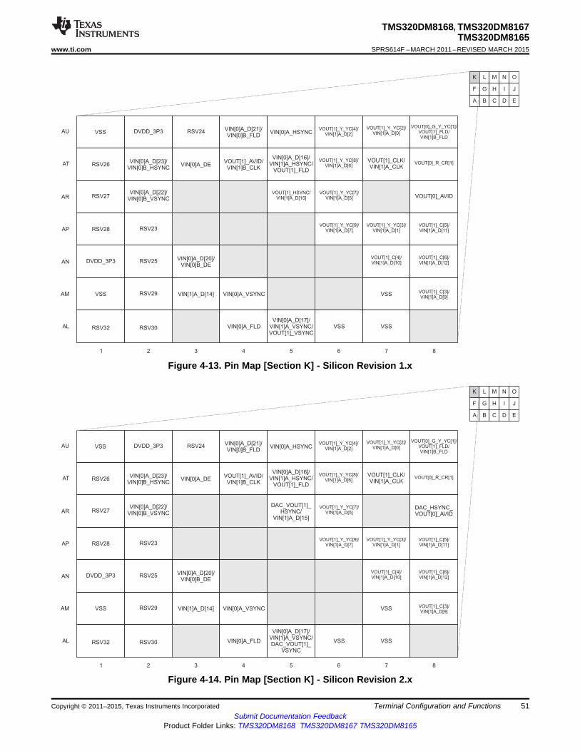
VSS DVDD_3P3 RSV24 VIN[0]A_D[21]/VIN[0]B_FLD
VIN[0]A_HSYNCVOUT[1]_Y_YC[4]/
VIN[1]A_D[2]
VOUT[1]_Y_YC[2]/VIN[1]A_D[0]
VOUT[0]_G_Y_YC[1]/VOUT[1]_FLD/VIN[1]B_FLD
RSV26VIN[0]A_D[23]/
VIN[0]B_HSYNCVIN[0]A_DE
VOUT[1]_AVID/VIN[1]B_CLK
VIN[0]A_D[16]/VIN[1]A_HSYNC/
VOUT[1]_FLD
VOUT[1]_Y_YC[8]/VIN[1]A_D[6]
VOUT[1]_CLK/VIN[1]A_CLK
VOUT[0]_R_CR[1]
RSV27VIN[0]A_D[22]/
VIN[0]B_VSYNC
DAC_VOUT[1]_HSYNC/
VIN[1]A_D[15]
VOUT[1]_Y_YC[7]/VIN[1]A_D[5]
DAC_HSYNC_VOUT[0]_AVID
AU
AT
AR
AP
AN
AM
AL
1 2 3 4 5 6 7 8
A B C
RSV28 RSV23VOUT[1]_Y_YC[9]/
VIN[1]A_D[7]VOUT[1]_Y_YC[3]/
VIN[1]A_D[1]VOUT[1]_C[5]/VIN[1]A_D[11]
DVDD_3P3 RSV25 VIN[0]A_D[20]/VIN[0]B_DE
VOUT[1]_C[4]/VIN[1]A_D[10]
VOUT[1]_C[6]/VIN[1]A_D[12]
F G H
D
I
K L M N
E
J
O
VSS RSV29 VIN[1]A_D[14] VIN[0]A_VSYNC VSS VOUT[1]_C[3]/VIN[1]A_D[9]
RSV32 RSV30 VIN[0]A_FLD
VIN[0]A_D[17]/VIN[1]A_VSYNC/DAC_VOUT[1]_
VSYNC
VSS VSS
VSS DVDD_3P3 RSV24 VIN[0]A_D[21]/VIN[0]B_FLD
VIN[0]A_HSYNCVOUT[1]_Y_YC[4]/
VIN[1]A_D[2]
VOUT[1]_Y_YC[2]/VIN[1]A_D[0]
VOUT[0]_G_Y_YC[1]/VOUT[1]_FLD/VIN[1]B_FLD
RSV26VIN[0]A_D[23]/
VIN[0]B_HSYNCVIN[0]A_DE
VOUT[1]_AVID/VIN[1]B_CLK
VIN[0]A_D[16]/VIN[1]A_HSYNC/
VOUT[1]_FLD
VOUT[1]_Y_YC[8]/VIN[1]A_D[6]
VOUT[1]_CLK/VIN[1]A_CLK
VOUT[0]_R_CR[1]
RSV27VIN[0]A_D[22]/
VIN[0]B_VSYNCVOUT[1]_HSYNC/
VIN[1]A_D[15]VOUT[1]_Y_YC[7]/
VIN[1]A_D[5] VOUT[0]_AVID
AU
AT
AR
AP
AN
AM
AL
1 2 3 4 5 6 7 8
A B C
RSV28 RSV23VOUT[1]_Y_YC[9]/
VIN[1]A_D[7]VOUT[1]_Y_YC[3]/
VIN[1]A_D[1]VOUT[1]_C[5]/VIN[1]A_D[11]
DVDD_3P3 RSV25 VIN[0]A_D[20]/VIN[0]B_DE
VOUT[1]_C[4]/VIN[1]A_D[10]
VOUT[1]_C[6]/VIN[1]A_D[12]
F G H
D
I
K L M N
E
J
O
VSS RSV29 VIN[1]A_D[14] VIN[0]A_VSYNC VSS VOUT[1]_C[3]/VIN[1]A_D[9]
RSV32 RSV30 VIN[0]A_FLDVIN[0]A_D[17]/
VIN[1]A_VSYNC/VOUT[1]_VSYNC
VSS VSS
TMS320DM8168, TMS320DM8167TMS320DM8165
www.ti.com SPRS614F –MARCH 2011–REVISED MARCH 2015
Figure 4-13. Pin Map [Section K] - Silicon Revision 1.x
Figure 4-14. Pin Map [Section K] - Silicon Revision 2.x
Copyright © 2011–2015, Texas Instruments Incorporated Terminal Configuration and Functions 51Submit Documentation Feedback
Product Folder Links: TMS320DM8168 TMS320DM8167 TMS320DM8165

VOUT[0]_R_CR[9]/VOUT[0]_B_CB_C[1]/
VOUT[1]_Y_YC[9]
VOUT[0]_R_CR[6]/VOUT[0]_G_Y_YC[0]/
VOUT[1]_Y_YC[6]DVDD_3P3 VSS VOUT[0]_G_Y_YC[8] VIN[0]A_D[15] VIN[0]A_D[14] VIN[0]A_D[12]
VOUT[0]_B_CB_C[1]/DAC_VOUT[1]_
HSYNC/VOUT[1]_AVID
VOUT[0]_R_CR[5]/VOUT[0]_AVID/
VOUT[1]_Y_YC[5]
VOUT[0]_R_CR[2]/VOUT[0]_HSYNC/VOUT[1]_Y_YC[2]
VOUT[0]_B_CB_C[9] VOUT[0]_G_Y_YC[7] VOUT[0]_CLK VIN[0]A_D[13] VIN[0]A_D[10]
VOUT[0]_B_CB_C[0]/VOUT[1]_C[9]/
VIN[1]B_HSYNC_DE
VOUT[0]_R_CR[3]/VOUT[0]_VSYNC/VOUT[1]_Y_YC[3]
VOUT[0]_G_Y_YC[9] VIN[0]A_CLK VSS
9 10 11 12 13 14 15 16
A B C
VOUT[0]_G_Y_YC[0]/DAC_VOUT[1]_
VSYNC/VIN[1]B_VSYNC
VOUT[0]_B_CB_C[2] VOUT[0]_G_Y_YC[3] VSS
VOUT[0]_VSYNC DVDD_3P3 VOUT[0]_B_CB_C[4] VSS VSS
F G H
D
I
K L M N
E
J
O
VOUT[0]_HSYNC VOUT[0]_B_CB_C[7] VOUT[0]_G_Y_YC[5] VSS VSS
DAC_VSYNC_VOUT[0]_FLD
VOUT[0]_R_CR[7]/VOUT[0]_G_Y_YC[1]/
VOUT[1]_Y_YC[7]VOUT[0]_B_CB_C[3] VOUT[0]_G_Y_YC[4] VSS VSS
AU
AT
AR
AP
AN
AM
AL
VOUT[0]_R_CR[9]/VOUT[0]_B_CB_C[1]/
VOUT[1]_Y_YC[9]
VOUT[0]_R_CR[6]/VOUT[0]_G_Y_YC[0]/
VOUT[1]_Y_YC[6]DVDD_3P3 VSS VOUT[0]_G_Y_YC[8] VIN[0]A_D[15] VIN[0]A_D[14] VIN[0]A_D[12]
VOUT[0]_B_CB_C[1]/VOUT[1]_HSYNC/
VOUT[1]_AVID
VOUT[0]_R_CR[5]/VOUT[0]_AVID/
VOUT[1]_Y_YC[5]
VOUT[0]_R_CR[2]/VOUT[0]_HSYNC/VOUT[1]_Y_YC[2]
VOUT[0]_B_CB_C[9] VOUT[0]_G_Y_YC[7] VOUT[0]_CLK VIN[0]A_D[13] VIN[0]A_D[10]
VOUT[0]_B_CB_C[0]/VOUT[1]_C[9]/
VIN[1]B_HSYNC_DE
VOUT[0]_R_CR[3]/VOUT[0]_VSYNC/VOUT[1]_Y_YC[3]
VOUT[0]_G_Y_YC[9] VIN[0]A_CLK VSS
9 10 11 12 13 14 15 16
A B C
VOUT[0]_G_Y_YC[0]/VOUT[1]_VSYNC/VIN[1]B_VSYNC
VOUT[0]_B_CB_C[2] VOUT[0]_G_Y_YC[3] VSS
VOUT[0]_VSYNC DVDD_3P3 VOUT[0]_B_CB_C[4] VSS VSS
F G H
D
I
K L M N
E
J
O
VOUT[0]_HSYNC VOUT[0]_B_CB_C[7] VOUT[0]_G_Y_YC[5] VSS VSS
VOUT[0]_FLDVOUT[0]_R_CR[7]/
VOUT[0]_G_Y_YC[1]/VOUT[1]_Y_YC[7]
VOUT[0]_B_CB_C[3] VOUT[0]_G_Y_YC[4] VSS VSS
AU
AT
AR
AP
AN
AM
AL
TMS320DM8168, TMS320DM8167TMS320DM8165SPRS614F –MARCH 2011–REVISED MARCH 2015 www.ti.com
Figure 4-15. Pin Map [Section L] - Silicon Revision 1.x
Figure 4-16. Pin Map [Section L] - Silicon Revision 2.x
52 Terminal Configuration and Functions Copyright © 2011–2015, Texas Instruments IncorporatedSubmit Documentation Feedback
Product Folder Links: TMS320DM8168 TMS320DM8167 TMS320DM8165
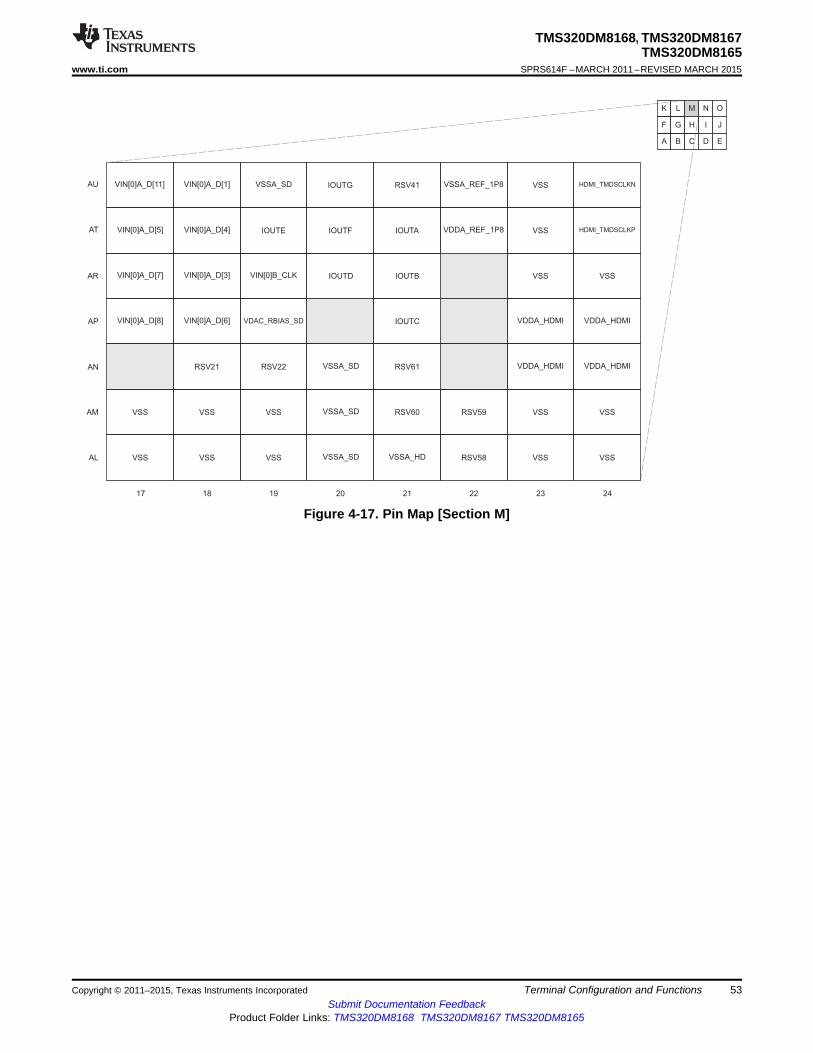
VIN[0]A_D[11] VIN[0]A_D[1] VSSA_SD IOUTG VSSA_REF_1P8 VSS HDMI_TMDSCLKN
VIN[0]A_D[5] VIN[0]A_D[4] IOUTE IOUTF IOUTA VDDA_REF_1P8 VSS HDMI_TMDSCLKP
VIN[0]A_D[7] VIN[0]A_D[3] VIN[0]B_CLK IOUTD IOUTB VSS VSS
17 18 19 20 21 22 23 24
A B C
VIN[0]A_D[8] VIN[0]A_D[6] VDAC_RBIAS_SD IOUTC VDDA_HDMI VDDA_HDMI
RSV21 RSV22 VSSA_SD VDDA_HDMI VDDA_HDMI
F G H
D
I
K L M N
E
J
O
VSS VSS VSS VSSA_SD VSS VSS
VSS VSS VSS VSSA_SD VSSA_HD VSS VSS
AU
AT
AR
AP
AN
AM
AL RSV58
RSV59RSV60
RSV61
RSV41
TMS320DM8168, TMS320DM8167TMS320DM8165
www.ti.com SPRS614F –MARCH 2011–REVISED MARCH 2015
Figure 4-17. Pin Map [Section M]
Copyright © 2011–2015, Texas Instruments Incorporated Terminal Configuration and Functions 53Submit Documentation Feedback
Product Folder Links: TMS320DM8168 TMS320DM8167 TMS320DM8165

HDMI_TMDSDN0 HDMI_TMDSDN1 HDMI_TMDSDN2 VSS DVDD_3P3 EMAC[1]_TXEN EMAC[1]_TXD[4] EMAC[1]_TXD[3]
HDMI_TMDSDP0 HDMI_TMDSDP1 HDMI_TMDSDP2 RSV40 RSV39 EMAC[1]_TXCLK EMAC[1]_TXD[5] EMAC[1]_TXD[2]
VSS VDDA_HDMI RSV38 EMAC[1]_COL EMAC[1]_TXD[1]
25 26 27 28 29 30 31 32
A B C
HDMI_CEC RSV37 EMAC[1]_TXD[6] EMAC[1]_TXD[0] EMAC1_RXD[7]
HDMI_EXTSWING DVDD_3P3 RSV36 EMAC[1]_RXER EMAC[1]_CRS
F G H
D
I
K L M N
E
J
O
VSS RSV33 EMAC[1]_TXD[7] VSS
HDMI_SCL RSV34 RSV35 VSS VSS
AU
AT
AR
AP
AN
AM
AL
TMS320DM8168, TMS320DM8167TMS320DM8165SPRS614F –MARCH 2011–REVISED MARCH 2015 www.ti.com
Figure 4-18. Pin Map [Section N]
54 Terminal Configuration and Functions Copyright © 2011–2015, Texas Instruments IncorporatedSubmit Documentation Feedback
Product Folder Links: TMS320DM8168 TMS320DM8167 TMS320DM8165

EMAC[1]_GMTCLK EMAC[1]_RXD[6] EMAC[1]_RXD[4] EMAC[1]_RXD[2] RSV9
EMAC[1]_RXDV EMAC1_RXD[3] EMAC1_RXD[1] EMAC1_RXD[0] EMAC[1]_RXCLK
EMAC[1]_RXD[5] MCA[2]_AXR[0]MCA[2]_AXR[1]/
MCB_DX
33 34 35 36 37
A B C
MCA[2]_AMUTE VSS
MCA[2]_AFSX/MCB_CLKS/MCB_FSX
MCA[2]_AHCLKX/MCB_CLKR
DVDD_3P3
F G H
D
I
K L M N
E
J
O
MCA[2]_AHCLKR/MCB_CLKS
MCA[2]_AFSR/MCB_CLKX/MCB_FSR
MCA[2]_ACLKX/MCB_CLKX
MCA[1]_AHCLKX
MCA[1]_AXR[0]MCA[2]_ACLKR/
MCB_CLKR/MCB_DR
MCA[1]_ACLKX MCA[1]_AHCLKR
AU
AT
AR
AP
AN
AM
AL
TMS320DM8168, TMS320DM8167TMS320DM8165
www.ti.com SPRS614F –MARCH 2011–REVISED MARCH 2015
Figure 4-19. Pin Map [Section O]
Copyright © 2011–2015, Texas Instruments Incorporated Terminal Configuration and Functions 55Submit Documentation Feedback
Product Folder Links: TMS320DM8168 TMS320DM8167 TMS320DM8165
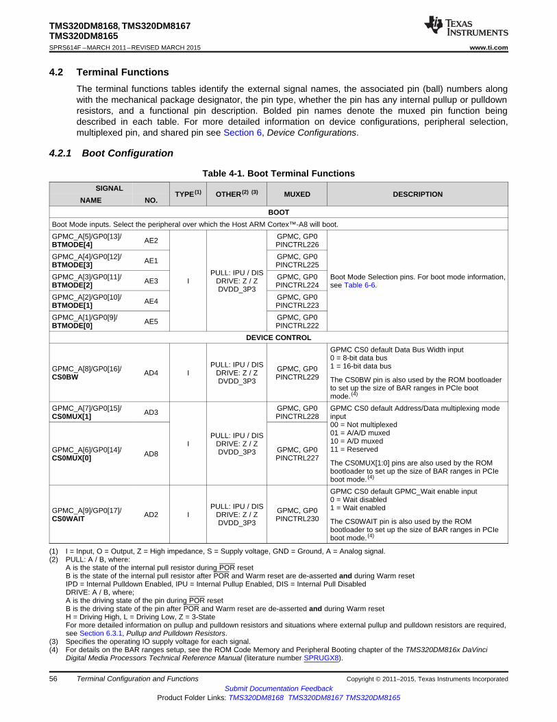
TMS320DM8168, TMS320DM8167TMS320DM8165SPRS614F –MARCH 2011–REVISED MARCH 2015 www.ti.com
4.2 Terminal FunctionsThe terminal functions tables identify the external signal names, the associated pin (ball) numbers alongwith the mechanical package designator, the pin type, whether the pin has any internal pullup or pulldownresistors, and a functional pin description. Bolded pin names denote the muxed pin function beingdescribed in each table. For more detailed information on device configurations, peripheral selection,multiplexed pin, and shared pin see Section 6, Device Configurations.
4.2.1 Boot Configuration
Table 4-1. Boot Terminal FunctionsSIGNAL
TYPE (1) OTHER (2) (3) MUXED DESCRIPTIONNAME NO.
BOOTBoot Mode inputs. Select the peripheral over which the Host ARM Cortex™-A8 will boot.GPMC_A[5]/GP0[13]/ GPMC, GP0AE2BTMODE[4] PINCTRL226GPMC_A[4]/GP0[12]/ GPMC, GP0AE1BTMODE[3] PINCTRL225
PULL: IPU / DISGPMC_A[3]/GP0[11]/ GPMC, GP0 Boot Mode Selection pins. For boot mode information,AE3 I DRIVE: Z / ZBTMODE[2] PINCTRL224 see Table 6-6.DVDD_3P3GPMC_A[2]/GP0[10]/ GPMC, GP0AE4BTMODE[1] PINCTRL223GPMC_A[1]/GP0[9]/ GPMC, GP0AE5BTMODE[0] PINCTRL222
DEVICE CONTROLGPMC CS0 default Data Bus Width input0 = 8-bit data bus
PULL: IPU / DIS 1 = 16-bit data busGPMC_A[8]/GP0[16]/ GPMC, GP0AD4 I DRIVE: Z / ZCS0BW PINCTRL229 The CS0BW pin is also used by the ROM bootloaderDVDD_3P3to set up the size of BAR ranges in PCIe bootmode. (4)
GPMC_A[7]/GP0[15]/ GPMC, GP0 GPMC CS0 default Address/Data multiplexing modeAD3CS0MUX[1] PINCTRL228 input00 = Not multiplexed01 = A/A/D muxedPULL: IPU / DIS10 = A/D muxedI DRIVE: Z / Z11 = ReservedGPMC_A[6]/GP0[14]/ GPMC, GP0DVDD_3P3AD8CS0MUX[0] PINCTRL227The CS0MUX[1:0] pins are also used by the ROMbootloader to set up the size of BAR ranges in PCIeboot mode. (4)
GPMC CS0 default GPMC_Wait enable input0 = Wait disabled
PULL: IPU / DIS 1 = Wait enabledGPMC_A[9]/GP0[17]/ GPMC, GP0AD2 I DRIVE: Z / ZCS0WAIT PINCTRL230 The CS0WAIT pin is also used by the ROMDVDD_3P3bootloader to set up the size of BAR ranges in PCIeboot mode. (4)
(1) I = Input, O = Output, Z = High impedance, S = Supply voltage, GND = Ground, A = Analog signal.(2) PULL: A / B, where:
A is the state of the internal pull resistor during POR resetB is the state of the internal pull resistor after POR and Warm reset are de-asserted and during Warm resetIPD = Internal Pulldown Enabled, IPU = Internal Pullup Enabled, DIS = Internal Pull DisabledDRIVE: A / B, where;A is the driving state of the pin during POR resetB is the driving state of the pin after POR and Warm reset are de-asserted and during Warm resetH = Driving High, L = Driving Low, Z = 3-StateFor more detailed information on pullup and pulldown resistors and situations where external pullup and pulldown resistors are required,see Section 6.3.1, Pullup and Pulldown Resistors.
(3) Specifies the operating IO supply voltage for each signal.(4) For details on the BAR ranges setup, see the ROM Code Memory and Peripheral Booting chapter of the TMS320DM816x DaVinci
Digital Media Processors Technical Reference Manual (literature number SPRUGX8).
56 Terminal Configuration and Functions Copyright © 2011–2015, Texas Instruments IncorporatedSubmit Documentation Feedback
Product Folder Links: TMS320DM8168 TMS320DM8167 TMS320DM8165

TMS320DM8168, TMS320DM8167TMS320DM8165
www.ti.com SPRS614F –MARCH 2011–REVISED MARCH 2015
4.2.2 DDR2 and DDR3 Memory Controller Signals
Table 4-2. DDR2 and DDR3 Memory Controller 0 Terminal FunctionsSIGNAL
TYPE (1) OTHER (2) DESCRIPTIONNAME NO.
DDR[0]_CLK[0] B12 O DVDD_DDR[0] DDR[0] Clock 0DDR[0]_CLK[0] A12 O DVDD_DDR[0] DDR[0] Negative Clock 0DDR[0]_CLK[1] A15 O DVDD_DDR[0] DDR[0] Clock 1DDR[0]_CLK[1] B15 O DVDD_DDR[0] DDR[0] Negative Clock 1DDR[0]_CKE C18 O DVDD_DDR[0] DDR[0] Clock EnableDDR[0]_WE E13 O DVDD_DDR[0] DDR[0] Write EnableDDR[0]_CS[0] B17 O DVDD_DDR[0] DDR[0] Chip Select 0DDR[0]_CS[1] F18 O DVDD_DDR[0] DDR[0] Chip Select 1DDR[0]_RAS D13 O DVDD_DDR[0] DDR[0] Row Address Strobe outputDDR[0]_CAS C13 O DVDD_DDR[0] DDR[0] Column Address Strobe outputDDR[0]_DQM[3] D9 O DVDD_DDR[0] DDR[0] Data Mask outputs
DDR[0]_DQM[3]: For upper byte data bus DDR[0]_D[31:24]DDR[0]_DQM[2] G9 O DVDD_DDR[0]DDR[0]_DQM[2]: For DDR[0]_D[23:16]
DDR[0]_DQM[1] B5 O DVDD_DDR[0] DDR[0]_DQM[1]: For DDR[0]_D[15:8]DDR[0]_DQM[0]: For lower byte data bus DDR[0]_D[7:0]DDR[0]_DQM[0] C2 O DVDD_DDR[0]
DDR[0]_DQS[3] B9 IO DVDD_DDR[0] Data strobe input/outputs for each byte of the 32-bit data bus. They areoutputs to the DDR[0] memory when writing and inputs when reading.DDR[0]_DQS[2] B8 IO DVDD_DDR[0] They are used to synchronize the data transfers.
DDR[0]_DQS[1] B4 IO DVDD_DDR[0] DDR[0]_DQS[3]: For upper byte data bus DDR[0]_D[31:24]DDR[0]_DQS[2]: For DDR[0]_D[23:16]DDR[0]_DQS[1]: For DDR[0]_D[15:8]DDR[0]_DQS[0] F4 IO DVDD_DDR[0]DDR[0]_DQS[0]: For lower byte data bus DDR[0]_D[7:0]
DDR[0]_DQS[3] A9 IO DVDD_DDR[0] Complementary data strobe input/outputs for each byte of the 32-bit databus. They are outputs to the DDR[0] memory when writing and inputsDDR[0]_DQS[2] A8 IO DVDD_DDR[0] when reading. They are used to synchronize the data transfers.
DDR[0]_DQS[1] A4 IO DVDD_DDR[0] DDR[0]_DQS[3]: For upper byte data bus DDR[0]_D[31:24]DDR[0]_DQS[2]: For DDR[0]_D[23:16]DDR[0]_DQS[1]: For DDR[0]_D[15:8]DDR[0]_DQS[0] E3 IO DVDD_DDR[0]DDR[0]_DQS[0]: For lower byte data bus DDR[0]_D[7:0]
DDR[0]_ODT[0] E18 O DVDD_DDR[0] DDR[0] On-Die Termination for Chip Select 0.DDR[0]_ODT[1] A16 O DVDD_DDR[0] DDR[0] On-Die Termination for Chip Select 1.DDR[0]_RST D18 O DVDD_DDR[0] DDR[0] Reset outputDDR[0]_BA[2] N15 O DVDD_DDR[0]DDR[0]_BA[1] B14 O DVDD_DDR[0] DDR[0] Bank Address outputsDDR[0]_BA[0] F13 O DVDD_DDR[0]
(1) I = Input, O = Output, Z = High impedance, S = Supply voltage, GND = Ground, A = Analog signal.(2) Specifies the operating IO supply voltage for each signal.
Copyright © 2011–2015, Texas Instruments Incorporated Terminal Configuration and Functions 57Submit Documentation Feedback
Product Folder Links: TMS320DM8168 TMS320DM8167 TMS320DM8165

TMS320DM8168, TMS320DM8167TMS320DM8165SPRS614F –MARCH 2011–REVISED MARCH 2015 www.ti.com
Table 4-2. DDR2 and DDR3 Memory Controller 0 Terminal Functions (continued)SIGNAL
TYPE (1) OTHER (2) DESCRIPTIONNAME NO.
DDR[0]_A[14] D17 O DVDD_DDR[0]DDR[0]_A[13] B16 O DVDD_DDR[0]DDR[0]_A[12] N16 O DVDD_DDR[0]DDR[0]_A[11] B13 O DVDD_DDR[0]DDR[0]_A[10] C14 O DVDD_DDR[0]DDR[0]_A[9] K13 O DVDD_DDR[0]DDR[0]_A[8] N14 O DVDD_DDR[0]DDR[0]_A[7] A14 O DVDD_DDR[0] DDR[0] Address BusDDR[0]_A[6] L13 O DVDD_DDR[0]DDR[0]_A[5] J13 O DVDD_DDR[0]DDR[0]_A[4] H13 O DVDD_DDR[0]DDR[0]_A[3] G13 O DVDD_DDR[0]DDR[0]_A[2] D15 O DVDD_DDR[0]DDR[0]_A[1] N17 O DVDD_DDR[0]DDR[0]_A[0] A13 O DVDD_DDR[0]DDR[0]_D[31] C9 IO DVDD_DDR[0]DDR[0]_D[30] J11 IO DVDD_DDR[0]DDR[0]_D[29] C11 IO DVDD_DDR[0]DDR[0]_D[28] G10 IO DVDD_DDR[0]DDR[0]_D[27] E8 IO DVDD_DDR[0]DDR[0]_D[26] B10 IO DVDD_DDR[0]DDR[0]_D[25] B11 IO DVDD_DDR[0]DDR[0]_D[24] E9 IO DVDD_DDR[0]
DDR[0] Data BusDDR[0]_D[23] E7 IO DVDD_DDR[0]DDR[0]_D[22] F9 IO DVDD_DDR[0]DDR[0]_D[21] D8 IO DVDD_DDR[0]DDR[0]_D[20] F8 IO DVDD_DDR[0]DDR[0]_D[19] B7 IO DVDD_DDR[0]DDR[0]_D[18] H10 IO DVDD_DDR[0]DDR[0]_D[17] A7 IO DVDD_DDR[0]DDR[0]_D[16] C8 IO DVDD_DDR[0]
58 Terminal Configuration and Functions Copyright © 2011–2015, Texas Instruments IncorporatedSubmit Documentation Feedback
Product Folder Links: TMS320DM8168 TMS320DM8167 TMS320DM8165

TMS320DM8168, TMS320DM8167TMS320DM8165
www.ti.com SPRS614F –MARCH 2011–REVISED MARCH 2015
Table 4-2. DDR2 and DDR3 Memory Controller 0 Terminal Functions (continued)SIGNAL
TYPE (1) OTHER (2) DESCRIPTIONNAME NO.
DDR[0]_D[15] B3 IO DVDD_DDR[0]DDR[0]_D[14] A3 IO DVDD_DDR[0]DDR[0]_D[13] B6 IO DVDD_DDR[0]DDR[0]_D[12] A5 IO DVDD_DDR[0]DDR[0]_D[11] D6 IO DVDD_DDR[0]DDR[0]_D[10] C6 IO DVDD_DDR[0]DDR[0]_D[9] D7 IO DVDD_DDR[0]DDR[0]_D[8] C5 IO DVDD_DDR[0]
DDR[0] Data BusDDR[0]_D[7] C1 IO DVDD_DDR[0]DDR[0]_D[6] F3 IO DVDD_DDR[0]DDR[0]_D[5] B2 IO DVDD_DDR[0]DDR[0]_D[4] D2 IO DVDD_DDR[0]DDR[0]_D[3] G4 IO DVDD_DDR[0]DDR[0]_D[2] E2 IO DVDD_DDR[0]DDR[0]_D[1] F2 IO DVDD_DDR[0]DDR[0]_D[0] B1 IO DVDD_DDR[0]DDR[0]_VTP A6 I DVDD_DDR[0] DDR VTP Compensation Resistor Connection
Copyright © 2011–2015, Texas Instruments Incorporated Terminal Configuration and Functions 59Submit Documentation Feedback
Product Folder Links: TMS320DM8168 TMS320DM8167 TMS320DM8165
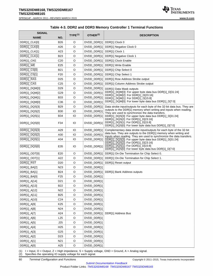
TMS320DM8168, TMS320DM8167TMS320DM8165SPRS614F –MARCH 2011–REVISED MARCH 2015 www.ti.com
Table 4-3. DDR2 and DDR3 Memory Controller 1 Terminal FunctionsSIGNAL
TYPE (1) OTHER (2) DESCRIPTIONNAME NO.
DDR[1]_CLK[0] B26 O DVDD_DDR[1] DDR[1] Clock 0DDR[1]_CLK[0] A26 O DVDD_DDR[1] DDR[1] Negative Clock 0DDR[1]_CLK[1] A23 O DVDD_DDR[1] DDR[1] Clock 1DDR[1]_CLK[1] B23 O DVDD_DDR[1] DDR[1] Negative Clock 1DDR[1]_CKE C20 O DVDD_DDR[1] DDR[1] Clock EnableDDR[1]_WE E25 O DVDD_DDR[1] DDR[1] Write EnableDDR[1]_CS[0] B21 O DVDD_DDR[1] DDR[1] Chip Select 0DDR[1]_CS[1] F20 O DVDD_DDR[1] DDR[1] Chip Select 1DDR[1]_RAS D25 O DVDD_DDR[1] DDR[1] Row Address Strobe outputDDR[1]_CAS C25 O DVDD_DDR[1] DDR[1] Column Address Strobe outputDDR[1]_DQM[3] D29 O DVDD_DDR[1] DDR[1] Data Mask outputs
DDR[1]_DQM[3]: For upper byte data bus DDR[1]_D[31:24]DDR[1]_DQM[2] G29 O DVDD_DDR[1]DDR[1]_DQM[2]: For DDR[1]_D[23:16]
DDR[1]_DQM[1] B33 O DVDD_DDR[1] DDR[1]_DQM[1]: For DDR[1]_D[15:8]DDR[1]_DQM[0]: For lower byte data bus DDR[1]_D[7:0]DDR[1]_DQM[0] C36 O DVDD_DDR[1]
DDR[1]_DQS[3] B29 O DVDD_DDR[1] Data strobe input/outputs for each byte of the 32-bit data bus. They areoutputs to the DDR[1] memory when writing and inputs when reading.DDR[1]_DQS[2] B30 IO DVDD_DDR[1] They are used to synchronize the data transfers.
DDR[1]_DQS[1] B34 IO DVDD_DDR[1] DDR[1]_DQS[3]: For upper byte data bus DDR[1]_D[31:24]DDR[1]_DQS[2]: For DDR[1]_D[23:16]DDR[1]_DQS[1]: For DDR[1]_D[15:8]DDR[1]_DQS[0] F34 IO DVDD_DDR[1]DDR[1]_DQS[0]: For lower byte data bus DDR[1]_D[7:0]
DDR[1]_DQS[3] A29 IO DVDD_DDR[1] Complementary data strobe input/outputs for each byte of the 32-bitdata bus. They are outputs to the DDR[1] memory when writing andDDR[1]_DQS[2] A30 IO DVDD_DDR[1] inputs when reading. They are used to synchronize the data transfers.
DDR[1]_DQS[1] A34 IO DVDD_DDR[1] DDR[1]_DQS[3]: For upper byte data bus DDR[1]_D[31:24]DDR[1]_DQS[2]: For DDR[1]_D[23:16]DDR[1]_DQS[1]: For DDR[1]_D[15:8]DDR[1]_DQS[0] E35 IO DVDD_DDR[1]DDR[1]_DQS[0]: For lower byte data bus DDR[1]_D[7:0]
DDR[1]_ODT[0] E20 O DVDD_DDR[1] DDR[1] On-Die Termination for Chip Select 0.DDR[1]_ODT[1] A22 O DVDD_DDR[1] DDR[1] On-Die Termination for Chip Select 1.DDR[1]_RST D20 O DVDD_DDR[1] DDR[1] Reset outputDDR[1]_BA[2] N23 O DVDD_DDR[1]DDR[1]_BA[1] B24 O DVDD_DDR[1] DDR[1] Bank Address outputsDDR[1]_BA[0] F25 O DVDD_DDR[1]DDR[1]_A[14] D21 O DVDD_DDR[1]DDR[1]_A[13] B22 O DVDD_DDR[1]DDR[1]_A[12] N22 O DVDD_DDR[1]DDR[1]_A[11] B25 O DVDD_DDR[1]DDR[1]_A[10] C24 O DVDD_DDR[1]DDR[1]_A[9] K25 O DVDD_DDR[1]DDR[1]_A[8] N24 O DVDD_DDR[1]DDR[1]_A[7] A24 O DVDD_DDR[1] DDR[1] Address BusDDR[1]_A[6] L25 O DVDD_DDR[1]DDR[1]_A[5] J25 O DVDD_DDR[1]DDR[1]_A[4] H25 O DVDD_DDR[1]DDR[1]_A[3] G25 O DVDD_DDR[1]DDR[1]_A[2] D23 O DVDD_DDR[1]DDR[1]_A[1] N21 O DVDD_DDR[1]DDR[1]_A[0] A25 O DVDD_DDR[1]
(1) I = Input, O = Output, Z = High impedance, S = Supply voltage, GND = Ground, A = Analog signal.(2) Specifies the operating IO supply voltage for each signal.
60 Terminal Configuration and Functions Copyright © 2011–2015, Texas Instruments IncorporatedSubmit Documentation Feedback
Product Folder Links: TMS320DM8168 TMS320DM8167 TMS320DM8165

TMS320DM8168, TMS320DM8167TMS320DM8165
www.ti.com SPRS614F –MARCH 2011–REVISED MARCH 2015
Table 4-3. DDR2 and DDR3 Memory Controller 1 Terminal Functions (continued)SIGNAL
TYPE (1) OTHER (2) DESCRIPTIONNAME NO.
DDR[1]_D[31] C29 IO DVDD_DDR[1]DDR[1]_D[30] J27 IO DVDD_DDR[1]DDR[1]_D[29] C27 IO DVDD_DDR[1]DDR[1]_D[28] G28 IO DVDD_DDR[1]DDR[1]_D[27] E30 IO DVDD_DDR[1]DDR[1]_D[26] B28 IO DVDD_DDR[1]DDR[1]_D[25] B27 IO DVDD_DDR[1]DDR[1]_D[24] E29 IO DVDD_DDR[1]
DDR[1] Data BusDDR[1]_D[23] E31 IO DVDD_DDR[1]DDR[1]_D[22] F29 IO DVDD_DDR[1]DDR[1]_D[21] D30 IO DVDD_DDR[1]DDR[1]_D[20] F30 IO DVDD_DDR[1]DDR[1]_D[19] B31 IO DVDD_DDR[1]DDR[1]_D[18] H28 IO DVDD_DDR[1]DDR[1]_D[17] A31 IO DVDD_DDR[1]DDR[1]_D[16] C30 IO DVDD_DDR[1]DDR[1]_D[15] B35 IO DVDD_DDR[1]DDR[1]_D[14] A35 IO DVDD_DDR[1]DDR[1]_D[13] B32 IO DVDD_DDR[1]DDR[1]_D[12] A33 IO DVDD_DDR[1]DDR[1]_D[11] D32 IO DVDD_DDR[1]DDR[1]_D[10] C32 IO DVDD_DDR[1]DDR[1]_D[9] D31 IO DVDD_DDR[1]DDR[1]_D[8] C33 IO DVDD_DDR[1]
DDR[1] Data BusDDR[1]_D[7] C37 IO DVDD_DDR[1]DDR[1]_D[6] F35 IO DVDD_DDR[1]DDR[1]_D[5] B36 IO DVDD_DDR[1]DDR[1]_D[4] D36 IO DVDD_DDR[1]DDR[1]_D[3] G34 IO DVDD_DDR[1]DDR[1]_D[2] E36 IO DVDD_DDR[1]DDR[1]_D[1] F36 IO DVDD_DDR[1]DDR[1]_D[0] B37 IO DVDD_DDR[1]DDR[1]_VTP A32 I DVDD_DDR[1] DDR VTP Compensation Resistor Connection
Copyright © 2011–2015, Texas Instruments Incorporated Terminal Configuration and Functions 61Submit Documentation Feedback
Product Folder Links: TMS320DM8168 TMS320DM8167 TMS320DM8165
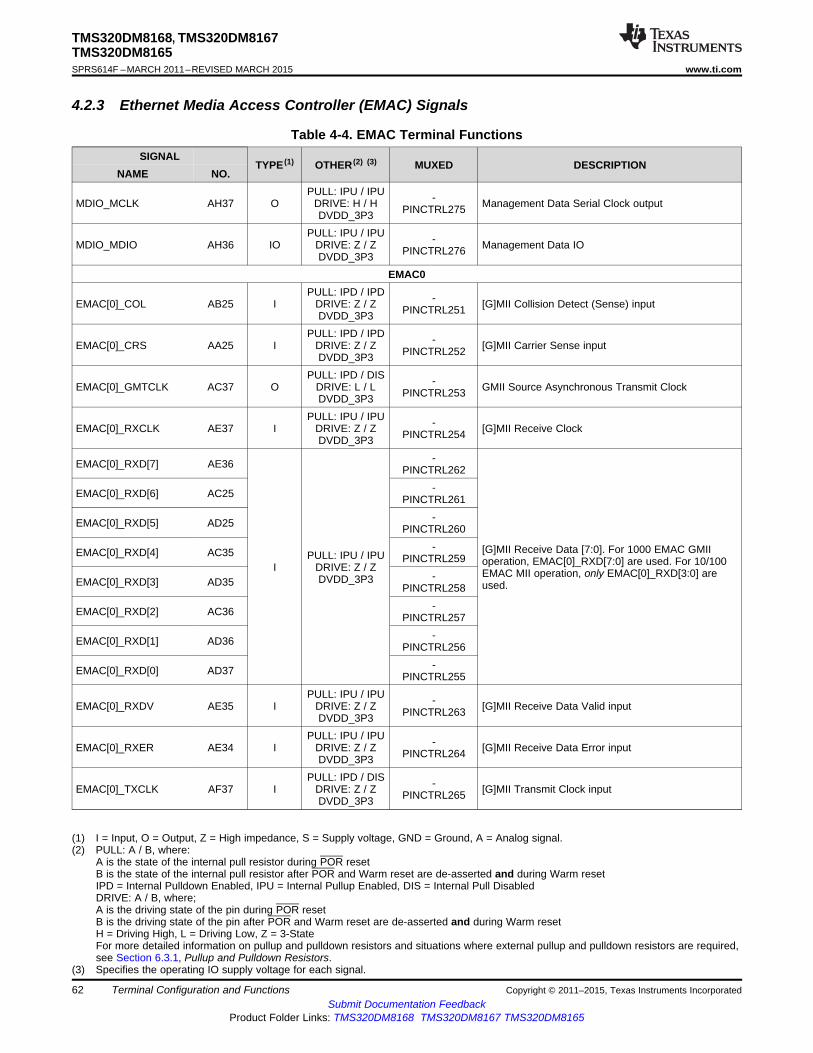
TMS320DM8168, TMS320DM8167TMS320DM8165SPRS614F –MARCH 2011–REVISED MARCH 2015 www.ti.com
4.2.3 Ethernet Media Access Controller (EMAC) Signals
Table 4-4. EMAC Terminal FunctionsSIGNAL
TYPE (1) OTHER (2) (3) MUXED DESCRIPTIONNAME NO.
PULL: IPU / IPU -MDIO_MCLK AH37 O DRIVE: H / H Management Data Serial Clock outputPINCTRL275DVDD_3P3PULL: IPU / IPU -MDIO_MDIO AH36 IO DRIVE: Z / Z Management Data IOPINCTRL276DVDD_3P3
EMAC0PULL: IPD / IPD -EMAC[0]_COL AB25 I DRIVE: Z / Z [G]MII Collision Detect (Sense) inputPINCTRL251DVDD_3P3PULL: IPD / IPD -EMAC[0]_CRS AA25 I DRIVE: Z / Z [G]MII Carrier Sense inputPINCTRL252DVDD_3P3PULL: IPD / DIS -EMAC[0]_GMTCLK AC37 O DRIVE: L / L GMII Source Asynchronous Transmit ClockPINCTRL253DVDD_3P3PULL: IPU / IPU -EMAC[0]_RXCLK AE37 I DRIVE: Z / Z [G]MII Receive ClockPINCTRL254DVDD_3P3
-EMAC[0]_RXD[7] AE36 PINCTRL262-EMAC[0]_RXD[6] AC25 PINCTRL261-EMAC[0]_RXD[5] AD25 PINCTRL260- [G]MII Receive Data [7:0]. For 1000 EMAC GMIIEMAC[0]_RXD[4] AC35 PULL: IPU / IPU PINCTRL259 operation, EMAC[0]_RXD[7:0] are used. For 10/100I DRIVE: Z / Z EMAC MII operation, only EMAC[0]_RXD[3:0] are-DVDD_3P3EMAC[0]_RXD[3] AD35 used.PINCTRL258-EMAC[0]_RXD[2] AC36 PINCTRL257-EMAC[0]_RXD[1] AD36 PINCTRL256-EMAC[0]_RXD[0] AD37 PINCTRL255
PULL: IPU / IPU -EMAC[0]_RXDV AE35 I DRIVE: Z / Z [G]MII Receive Data Valid inputPINCTRL263DVDD_3P3PULL: IPU / IPU -EMAC[0]_RXER AE34 I DRIVE: Z / Z [G]MII Receive Data Error inputPINCTRL264DVDD_3P3PULL: IPD / DIS -EMAC[0]_TXCLK AF37 I DRIVE: Z / Z [G]MII Transmit Clock inputPINCTRL265DVDD_3P3
(1) I = Input, O = Output, Z = High impedance, S = Supply voltage, GND = Ground, A = Analog signal.(2) PULL: A / B, where:
A is the state of the internal pull resistor during POR resetB is the state of the internal pull resistor after POR and Warm reset are de-asserted and during Warm resetIPD = Internal Pulldown Enabled, IPU = Internal Pullup Enabled, DIS = Internal Pull DisabledDRIVE: A / B, where;A is the driving state of the pin during POR resetB is the driving state of the pin after POR and Warm reset are de-asserted and during Warm resetH = Driving High, L = Driving Low, Z = 3-StateFor more detailed information on pullup and pulldown resistors and situations where external pullup and pulldown resistors are required,see Section 6.3.1, Pullup and Pulldown Resistors.
(3) Specifies the operating IO supply voltage for each signal.
62 Terminal Configuration and Functions Copyright © 2011–2015, Texas Instruments IncorporatedSubmit Documentation Feedback
Product Folder Links: TMS320DM8168 TMS320DM8167 TMS320DM8165

TMS320DM8168, TMS320DM8167TMS320DM8165
www.ti.com SPRS614F –MARCH 2011–REVISED MARCH 2015
Table 4-4. EMAC Terminal Functions (continued)SIGNAL
TYPE (1) OTHER (2) (3) MUXED DESCRIPTIONNAME NO.
-EMAC[0]_TXD[7] AG35 PINCTRL273-EMAC[0]_TXD[6] AG36 PINCTRL272-EMAC[0]_TXD[5] AF36 PINCTRL271- [G]MII Transmit Data [7:0]. For 1000 EMAC GMIIEMAC[0]_TXD[4] AG28 PULL: IPD / DIS PINCTRL270 operation, EMAC[0]_TXD[7:0] are used. For 10/100O DRIVE: L / L EMAC MII operation, only EMAC[0]_TXD[3:0] are-DVDD_3P3EMAC[0]_TXD[3] AE30 used.PINCTRL269-EMAC[0]_TXD[2] AE31 PINCTRL268-EMAC[0]_TXD[1] AE32 PINCTRL267-EMAC[0]_TXD[0] AE33 PINCTRL266
PULL: IPD / DIS -EMAC[0]_TXEN AG37 O DRIVE: L / L [G]MII Transmit Data Enable outputPINCTRL274DVDD_3P3EMAC1
PULL: IPD / DIS -EMAC[1]_COL AR30 I DRIVE: L / L [G]MII Collision Detect (Sense) inputPINCTRL72DVDD_3P3PULL: IPD / IPD -EMAC[1]_CRS AN31 I DRIVE: Z / Z [G]MII Carrier Sense inputPINCTRL73DVDD_3P3PULL: IPD / DIS -EMAC[1]_GMTCLK AU33 O DRIVE: Z / Z GMII Source Asynchronous Transmit ClockPINCTRL61DVDD_3P3PULL: IPD / IPD -EMAC[1]_RXCLK AT37 I DRIVE: Z / Z [G]MII Receive ClockPINCTRL51DVDD_3P3
-EMAC[1]_RXD[7] AP32 PINCTRL59-EMAC[1]_RXD[6] AU34 PINCTRL58-EMAC[1]_RXD[5] AR33 PINCTRL57- [G]MII Receive Data [7:0]. For 1000 EMAC GMIIEMAC[1]_RXD[4] AU35 PULL: IPD / IPD PINCTRL56 operation, EMAC[1]_RXD[7:0] are used. For 10/100I DRIVE: Z / Z EMAC MII operation, only EMAC[1]_RXD[3:0] are-DVDD_3P3EMAC[1]_RXD[3] AT34 used.PINCTRL55-EMAC[1]_RXD[2] AU36 PINCTRL54-EMAC[1]_RXD[1] AT35 PINCTRL53-EMAC[1]_RXD[0] AT36 PINCTRL52
PULL: IPD / IPD -EMAC[1]_RXDV AT33 I DRIVE: Z / Z [G]MII Receive Data Valid inputPINCTRL60DVDD_3P3PULL: IPD / DIS -EMAC[1]_RXER AN30 I DRIVE: L / L [G]MII Receive Data Error inputPINCTRL74DVDD_3P3
Copyright © 2011–2015, Texas Instruments Incorporated Terminal Configuration and Functions 63Submit Documentation Feedback
Product Folder Links: TMS320DM8168 TMS320DM8167 TMS320DM8165

TMS320DM8168, TMS320DM8167TMS320DM8165SPRS614F –MARCH 2011–REVISED MARCH 2015 www.ti.com
Table 4-4. EMAC Terminal Functions (continued)SIGNAL
TYPE (1) OTHER (2) (3) MUXED DESCRIPTIONNAME NO.
PULL: IPD / DIS -EMAC[1]_TXCLK AT30 I DRIVE: L / L [G]MII Transmit Clock inputPINCTRL71DVDD_3P3-EMAC[1]_TXD[7] AM30 PINCTRL69-EMAC[1]_TXD[6] AP30 PINCTRL68-EMAC[1]_TXD[5] AT31 PINCTRL67- [G]MII Transmit Data [7:0]. For 1000 EMAC GMIIEMAC[1]_TXD[4] AU31 PULL: IPD / DIS PINCTRL66 operation, EMAC[1]_TXD[7:0] are used. For 10/100O DRIVE: Z / Z EMAC MII operation, only EMAC[1]_TXD[3:0] are-DVDD_3P3EMAC[1]_TXD[3] AU32 used.PINCTRL65-EMAC[1]_TXD[2] AT32 PINCTRL64-EMAC[1]_TXD[1] AR32 PINCTRL63-EMAC[1]_TXD[0] AP31 PINCTRL62
PULL: IPD / DIS -EMAC[1]_TXEN AU30 O DRIVE: Z / Z [G]MII Transmit Data Enable outputPINCTRL70DVDD_3P3
64 Terminal Configuration and Functions Copyright © 2011–2015, Texas Instruments IncorporatedSubmit Documentation Feedback
Product Folder Links: TMS320DM8168 TMS320DM8167 TMS320DM8165
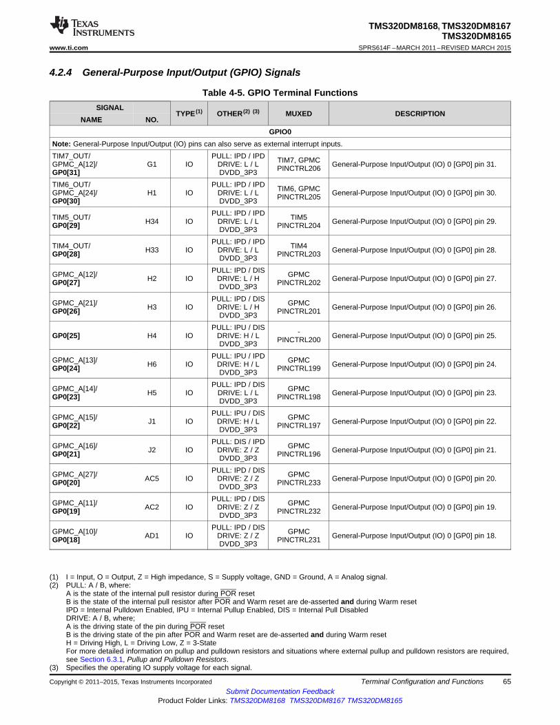
TMS320DM8168, TMS320DM8167TMS320DM8165
www.ti.com SPRS614F –MARCH 2011–REVISED MARCH 2015
4.2.4 General-Purpose Input/Output (GPIO) Signals
Table 4-5. GPIO Terminal FunctionsSIGNAL
TYPE (1) OTHER (2) (3) MUXED DESCRIPTIONNAME NO.
GPIO0Note: General-Purpose Input/Output (IO) pins can also serve as external interrupt inputs.TIM7_OUT/ PULL: IPD / IPD TIM7, GPMCGPMC_A[12]/ G1 IO DRIVE: L / L General-Purpose Input/Output (IO) 0 [GP0] pin 31.PINCTRL206GP0[31] DVDD_3P3TIM6_OUT/ PULL: IPD / IPD TIM6, GPMCGPMC_A[24]/ H1 IO DRIVE: L / L General-Purpose Input/Output (IO) 0 [GP0] pin 30.PINCTRL205GP0[30] DVDD_3P3
PULL: IPD / IPDTIM5_OUT/ TIM5H34 IO DRIVE: L / L General-Purpose Input/Output (IO) 0 [GP0] pin 29.GP0[29] PINCTRL204DVDD_3P3PULL: IPD / IPDTIM4_OUT/ TIM4H33 IO DRIVE: L / L General-Purpose Input/Output (IO) 0 [GP0] pin 28.GP0[28] PINCTRL203DVDD_3P3PULL: IPD / DISGPMC_A[12]/ GPMCH2 IO DRIVE: L / H General-Purpose Input/Output (IO) 0 [GP0] pin 27.GP0[27] PINCTRL202DVDD_3P3PULL: IPD / DISGPMC_A[21]/ GPMCH3 IO DRIVE: L / H General-Purpose Input/Output (IO) 0 [GP0] pin 26.GP0[26] PINCTRL201DVDD_3P3PULL: IPU / DIS -GP0[25] H4 IO DRIVE: H / L General-Purpose Input/Output (IO) 0 [GP0] pin 25.PINCTRL200DVDD_3P3PULL: IPU / IPDGPMC_A[13]/ GPMCH6 IO DRIVE: H / L General-Purpose Input/Output (IO) 0 [GP0] pin 24.GP0[24] PINCTRL199DVDD_3P3PULL: IPD / DISGPMC_A[14]/ GPMCH5 IO DRIVE: L / L General-Purpose Input/Output (IO) 0 [GP0] pin 23.GP0[23] PINCTRL198DVDD_3P3PULL: IPU / DISGPMC_A[15]/ GPMCJ1 IO DRIVE: H / L General-Purpose Input/Output (IO) 0 [GP0] pin 22.GP0[22] PINCTRL197DVDD_3P3PULL: DIS / IPDGPMC_A[16]/ GPMCJ2 IO DRIVE: Z / Z General-Purpose Input/Output (IO) 0 [GP0] pin 21.GP0[21] PINCTRL196DVDD_3P3PULL: IPD / DISGPMC_A[27]/ GPMCAC5 IO DRIVE: Z / Z General-Purpose Input/Output (IO) 0 [GP0] pin 20.GP0[20] PINCTRL233DVDD_3P3PULL: IPD / DISGPMC_A[11]/ GPMCAC2 IO DRIVE: Z / Z General-Purpose Input/Output (IO) 0 [GP0] pin 19.GP0[19] PINCTRL232DVDD_3P3PULL: IPD / DISGPMC_A[10]/ GPMCAD1 IO DRIVE: Z / Z General-Purpose Input/Output (IO) 0 [GP0] pin 18.GP0[18] PINCTRL231DVDD_3P3
(1) I = Input, O = Output, Z = High impedance, S = Supply voltage, GND = Ground, A = Analog signal.(2) PULL: A / B, where:
A is the state of the internal pull resistor during POR resetB is the state of the internal pull resistor after POR and Warm reset are de-asserted and during Warm resetIPD = Internal Pulldown Enabled, IPU = Internal Pullup Enabled, DIS = Internal Pull DisabledDRIVE: A / B, where;A is the driving state of the pin during POR resetB is the driving state of the pin after POR and Warm reset are de-asserted and during Warm resetH = Driving High, L = Driving Low, Z = 3-StateFor more detailed information on pullup and pulldown resistors and situations where external pullup and pulldown resistors are required,see Section 6.3.1, Pullup and Pulldown Resistors.
(3) Specifies the operating IO supply voltage for each signal.
Copyright © 2011–2015, Texas Instruments Incorporated Terminal Configuration and Functions 65Submit Documentation Feedback
Product Folder Links: TMS320DM8168 TMS320DM8167 TMS320DM8165
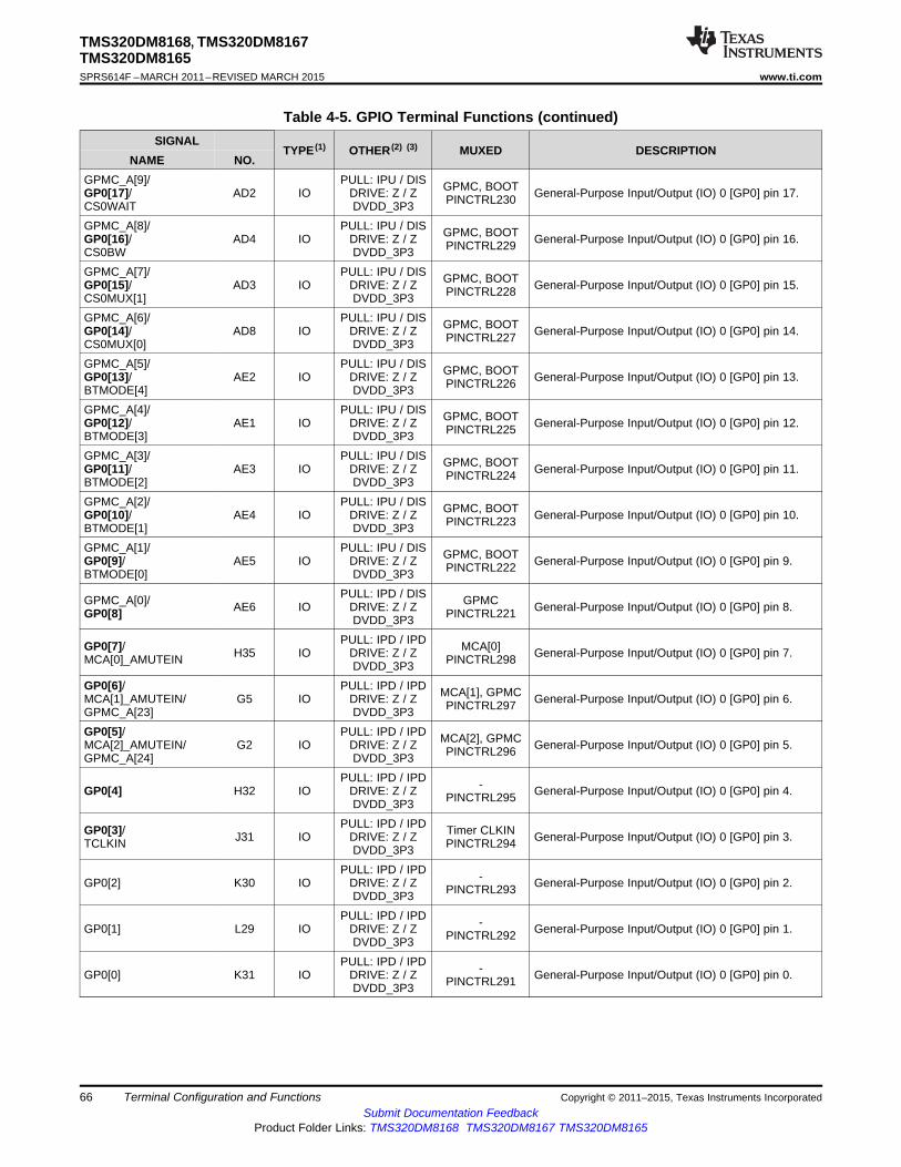
TMS320DM8168, TMS320DM8167TMS320DM8165SPRS614F –MARCH 2011–REVISED MARCH 2015 www.ti.com
Table 4-5. GPIO Terminal Functions (continued)SIGNAL
TYPE (1) OTHER (2) (3) MUXED DESCRIPTIONNAME NO.
GPMC_A[9]/ PULL: IPU / DIS GPMC, BOOTGP0[17]/ AD2 IO DRIVE: Z / Z General-Purpose Input/Output (IO) 0 [GP0] pin 17.PINCTRL230CS0WAIT DVDD_3P3GPMC_A[8]/ PULL: IPU / DIS GPMC, BOOTGP0[16]/ AD4 IO DRIVE: Z / Z General-Purpose Input/Output (IO) 0 [GP0] pin 16.PINCTRL229CS0BW DVDD_3P3GPMC_A[7]/ PULL: IPU / DIS GPMC, BOOTGP0[15]/ AD3 IO DRIVE: Z / Z General-Purpose Input/Output (IO) 0 [GP0] pin 15.PINCTRL228CS0MUX[1] DVDD_3P3GPMC_A[6]/ PULL: IPU / DIS GPMC, BOOTGP0[14]/ AD8 IO DRIVE: Z / Z General-Purpose Input/Output (IO) 0 [GP0] pin 14.PINCTRL227CS0MUX[0] DVDD_3P3GPMC_A[5]/ PULL: IPU / DIS GPMC, BOOTGP0[13]/ AE2 IO DRIVE: Z / Z General-Purpose Input/Output (IO) 0 [GP0] pin 13.PINCTRL226BTMODE[4] DVDD_3P3GPMC_A[4]/ PULL: IPU / DIS GPMC, BOOTGP0[12]/ AE1 IO DRIVE: Z / Z General-Purpose Input/Output (IO) 0 [GP0] pin 12.PINCTRL225BTMODE[3] DVDD_3P3GPMC_A[3]/ PULL: IPU / DIS GPMC, BOOTGP0[11]/ AE3 IO DRIVE: Z / Z General-Purpose Input/Output (IO) 0 [GP0] pin 11.PINCTRL224BTMODE[2] DVDD_3P3GPMC_A[2]/ PULL: IPU / DIS GPMC, BOOTGP0[10]/ AE4 IO DRIVE: Z / Z General-Purpose Input/Output (IO) 0 [GP0] pin 10.PINCTRL223BTMODE[1] DVDD_3P3GPMC_A[1]/ PULL: IPU / DIS GPMC, BOOTGP0[9]/ AE5 IO DRIVE: Z / Z General-Purpose Input/Output (IO) 0 [GP0] pin 9.PINCTRL222BTMODE[0] DVDD_3P3
PULL: IPD / DISGPMC_A[0]/ GPMCAE6 IO DRIVE: Z / Z General-Purpose Input/Output (IO) 0 [GP0] pin 8.GP0[8] PINCTRL221DVDD_3P3PULL: IPD / IPDGP0[7]/ MCA[0]H35 IO DRIVE: Z / Z General-Purpose Input/Output (IO) 0 [GP0] pin 7.MCA[0]_AMUTEIN PINCTRL298DVDD_3P3
GP0[6]/ PULL: IPD / IPD MCA[1], GPMCMCA[1]_AMUTEIN/ G5 IO DRIVE: Z / Z General-Purpose Input/Output (IO) 0 [GP0] pin 6.PINCTRL297GPMC_A[23] DVDD_3P3GP0[5]/ PULL: IPD / IPD MCA[2], GPMCMCA[2]_AMUTEIN/ G2 IO DRIVE: Z / Z General-Purpose Input/Output (IO) 0 [GP0] pin 5.PINCTRL296GPMC_A[24] DVDD_3P3
PULL: IPD / IPD -GP0[4] H32 IO DRIVE: Z / Z General-Purpose Input/Output (IO) 0 [GP0] pin 4.PINCTRL295DVDD_3P3PULL: IPD / IPDGP0[3]/ Timer CLKINJ31 IO DRIVE: Z / Z General-Purpose Input/Output (IO) 0 [GP0] pin 3.TCLKIN PINCTRL294DVDD_3P3PULL: IPD / IPD -GP0[2] K30 IO DRIVE: Z / Z General-Purpose Input/Output (IO) 0 [GP0] pin 2.PINCTRL293DVDD_3P3PULL: IPD / IPD -GP0[1] L29 IO DRIVE: Z / Z General-Purpose Input/Output (IO) 0 [GP0] pin 1.PINCTRL292DVDD_3P3PULL: IPD / IPD -GP0[0] K31 IO DRIVE: Z / Z General-Purpose Input/Output (IO) 0 [GP0] pin 0.PINCTRL291DVDD_3P3
66 Terminal Configuration and Functions Copyright © 2011–2015, Texas Instruments IncorporatedSubmit Documentation Feedback
Product Folder Links: TMS320DM8168 TMS320DM8167 TMS320DM8165

TMS320DM8168, TMS320DM8167TMS320DM8165
www.ti.com SPRS614F –MARCH 2011–REVISED MARCH 2015
Table 4-5. GPIO Terminal Functions (continued)SIGNAL
TYPE (1) OTHER (2) (3) MUXED DESCRIPTIONNAME NO.
GPIO1Note: General-Purpose Input/Output (IO) pins can also serve as external interrupt inputs.GP1[31]/SATA_ACT1_LED PULL: IPD / IPD SATA(silicon revision 1.x) J33 IO DRIVE: Z / Z General-Purpose Input/Output (IO) 1 [GP1] pin 31.PINCTRL300SATA_ACT0_LED DVDD_3P3(silicon revision 2.x)GP1[30]/SATA_ACT0_LED PULL: IPD / IPD SATA(silicon revision 1.x) J32 IO DRIVE: Z / Z General-Purpose Input/Output (IO) 1 [GP1] pin 30.PINCTRL299SATA_ACT1_LED DVDD_3P3(silicon revision 2.x)
PULL: IPD / DISGPMC_CLK/ GPMCV1 IO DRIVE: L / L General-Purpose Input/Output (IO) 1 [GP1] pin 29.GP1[29] PINCTRL250DVDD_3P3PULL: IPU / IPUUART0_CTS/ UART0N7 IO DRIVE: Z / Z General-Purpose Input/Output (IO) 1 [GP1] pin 28.GP1[28] PINCTRL176DVDD_3P3PULL: IPU / DISUART0_RTS/ UART0N9 IO DRIVE: H / H General-Purpose Input/Output (IO) 1 [GP1] pin 27.GP1[27] PINCTRL175DVDD_3P3
UART1_CTS/ PULL: IPU / IPUGPMC_A[13]/ UART1, GPMCL3 IO DRIVE: Z / Z General-Purpose Input/Output (IO) 1 [GP1] pin 26.GPMC_A[17]/ PINCTRL184DVDD_3P3GP1[26]UART1_RTS/ PULL: IPU / DISGPMC_A[14]/ UART1, GPMCM2 IO DRIVE: H / H General-Purpose Input/Output (IO) 1 [GP1] pin 25.GPMC_A[18]/ PINCTRL183DVDD_3P3GP1[25]UART2_CTS/ PULL: IPU / IPUGPMC_A[16]/ UART2, GPMCK7 IO DRIVE: Z / Z General-Purpose Input/Output (IO) 1 [GP1] pin 24.GPMC_A[25]/ PINCTRL188DVDD_3P3GP1[24]UART2_RTS/ PULL: IPU / DISGPMC_A[15]/ UART2, GPMCL9 IO DRIVE: H / H General-Purpose Input/Output (IO) 1 [GP1] pin 23.GPMC_A[26]/ PINCTRL187DVDD_3P3GP1[23]SPI_SCS[3]/ PULL: DIS / IPU SPI, GPMCGPMC_A[21]/ P1 IO DRIVE: Z / Z General-Purpose Input/Output (IO) 1 [GP1] pin 22.PINCTRL170GP1[22] DVDD_3P3
PULL: IPU / IPUGPMC_CS[4]/ GPMCAG3 IO DRIVE: H / H General-Purpose Input/Output (IO) 1 [GP1] pin 21.GP1[21] PINCTRL211DVDD_3P3PULL: IPD / DISGPMC_DIR/ GPMCAE7 IO DRIVE: L / H General-Purpose Input/Output (IO) 1 [GP1] pin 20.GP1[20] PINCTRL218DVDD_3P3
UART0_RIN/ PULL: IPU / IPUGPMC_A[17]/ UART0, GPMCN3 IO DRIVE: Z / Z General-Purpose Input/Output (IO) 1 [GP1] pin 19.GPMC_A[22]/ PINCTRL180DVDD_3P3GP1[19]UART0_DCD/ PULL: IPU / IPUGPMC_A[18]/ UART0, GPMCN5 IO DRIVE: Z / Z General-Purpose Input/Output (IO) 1 [GP1] pin 18.GPMC_A[23]/ PINCTRL179DVDD_3P3GP1[18]UART0_DSR/ PULL: IPU / IPUGPMC_A[19]/ UART0, GPMCN4 IO DRIVE: Z / Z General-Purpose Input/Output (IO) 1 [GP1] pin 17.GPMC_A[24]/ PINCTRL178DVDD_3P3GP1[17]
Copyright © 2011–2015, Texas Instruments Incorporated Terminal Configuration and Functions 67Submit Documentation Feedback
Product Folder Links: TMS320DM8168 TMS320DM8167 TMS320DM8165
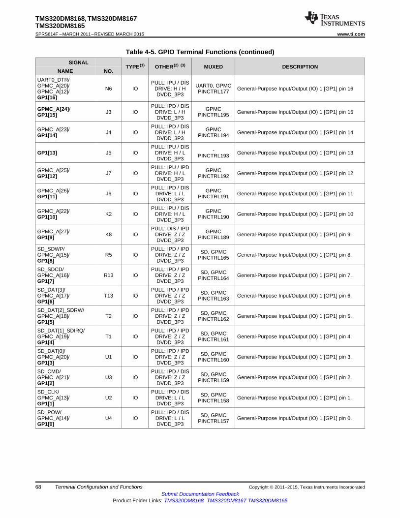
TMS320DM8168, TMS320DM8167TMS320DM8165SPRS614F –MARCH 2011–REVISED MARCH 2015 www.ti.com
Table 4-5. GPIO Terminal Functions (continued)SIGNAL
TYPE (1) OTHER (2) (3) MUXED DESCRIPTIONNAME NO.
UART0_DTR/ PULL: IPU / DISGPMC_A[20]/ UART0, GPMCN6 IO DRIVE: H / H General-Purpose Input/Output (IO) 1 [GP1] pin 16.GPMC_A[12]/ PINCTRL177DVDD_3P3GP1[16]PULL: IPD / DISGPMC_A[24]/ GPMCJ3 IO DRIVE: L / H General-Purpose Input/Output (IO) 1 [GP1] pin 15.GP1[15] PINCTRL195DVDD_3P3PULL: IPD / DISGPMC_A[23]/ GPMCJ4 IO DRIVE: L / H General-Purpose Input/Output (IO) 1 [GP1] pin 14.GP1[14] PINCTRL194DVDD_3P3PULL: IPU / DIS -GP1[13] J5 IO DRIVE: H / L General-Purpose Input/Output (IO) 1 [GP1] pin 13.PINCTRL193DVDD_3P3PULL: IPU / IPDGPMC_A[25]/ GPMCJ7 IO DRIVE: H / L General-Purpose Input/Output (IO) 1 [GP1] pin 12.GP1[12] PINCTRL192DVDD_3P3PULL: IPD / DISGPMC_A[26]/ GPMCJ6 IO DRIVE: L / L General-Purpose Input/Output (IO) 1 [GP1] pin 11.GP1[11] PINCTRL191DVDD_3P3PULL: IPU / DISGPMC_A[22]/ GPMCK2 IO DRIVE: H / L General-Purpose Input/Output (IO) 1 [GP1] pin 10.GP1[10] PINCTRL190DVDD_3P3PULL: DIS / IPDGPMC_A[27]/ GPMCK8 IO DRIVE: Z / Z General-Purpose Input/Output (IO) 1 [GP1] pin 9.GP1[9] PINCTRL189DVDD_3P3
SD_SDWP/ PULL: IPD / IPD SD, GPMCGPMC_A[15]/ R5 IO DRIVE: Z / Z General-Purpose Input/Output (IO) 1 [GP1] pin 8.PINCTRL165GP1[8] DVDD_3P3SD_SDCD/ PULL: IPD / IPD SD, GPMCGPMC_A[16]/ R13 IO DRIVE: Z / Z General-Purpose Input/Output (IO) 1 [GP1] pin 7.PINCTRL164GP1[7] DVDD_3P3SD_DAT[3]/ PULL: IPD / IPD SD, GPMCGPMC_A[17]/ T13 IO DRIVE: Z / Z General-Purpose Input/Output (IO) 1 [GP1] pin 6.PINCTRL163GP1[6] DVDD_3P3SD_DAT[2]_SDRW/ PULL: IPD / IPD SD, GPMCGPMC_A[18]/ T2 IO DRIVE: Z / Z General-Purpose Input/Output (IO) 1 [GP1] pin 5.PINCTRL162GP1[5] DVDD_3P3SD_DAT[1]_SDIRQ/ PULL: IPD / IPD SD, GPMCGPMC_A[19]/ T1 IO DRIVE: Z / Z General-Purpose Input/Output (IO) 1 [GP1] pin 4.PINCTRL161GP1[4] DVDD_3P3SD_DAT[0]/ PULL: IPD / IPD SD, GPMCGPMC_A[20]/ U1 IO DRIVE: Z / Z General-Purpose Input/Output (IO) 1 [GP1] pin 3.PINCTRL160GP1[3] DVDD_3P3SD_CMD/ PULL: IPD / DIS SD, GPMCGPMC_A[21]/ U3 IO DRIVE: Z / Z General-Purpose Input/Output (IO) 1 [GP1] pin 2.PINCTRL159GP1[2] DVDD_3P3SD_CLK/ PULL: IPD / DIS SD, GPMCGPMC_A[13]/ U2 IO DRIVE: L / L General-Purpose Input/Output (IO) 1 [GP1] pin 1.PINCTRL158GP1[1] DVDD_3P3SD_POW/ PULL: IPD / DIS SD, GPMCGPMC_A[14]/ U4 IO DRIVE: L / L General-Purpose Input/Output (IO) 1 [GP1] pin 0.PINCTRL157GP1[0] DVDD_3P3
68 Terminal Configuration and Functions Copyright © 2011–2015, Texas Instruments IncorporatedSubmit Documentation Feedback
Product Folder Links: TMS320DM8168 TMS320DM8167 TMS320DM8165

TMS320DM8168, TMS320DM8167TMS320DM8165
www.ti.com SPRS614F –MARCH 2011–REVISED MARCH 2015
4.2.5 General-Purpose Memory Controller (GPMC) Signals
Table 4-6. GPMC Terminal FunctionsSIGNAL
TYPE (1) OTHER (2) (3) MUXED DESCRIPTIONNAME NO.
PULL: IPD / DISGPMC_CLK/ V1 O DRIVE: L / L GP1 GPMC Clock outputGP1[29] DVDD_3P3PULL: IPU / IPUGPMC_CS[5] / GPMCAG1 O DRIVE: H / H GPMC Chip Select 5GPMC_A[12] PINCTRL212DVDD_3P3PULL: IPU / IPUGPMC_CS[4] / GP1AG3 O DRIVE: H / H GPMC Chip Select 4GP1[21] PINCTRL211DVDD_3P3PULL: IPU / IPU -GPMC_CS[3] AG9 O DRIVE: H / H GPMC Chip Select 3PINCTRL210DVDD_3P3PULL: IPU / IPU -GPMC_CS[2] AH2 O DRIVE: H / H GPMC Chip Select 2PINCTRL209DVDD_3P3PULL: IPU / IPU -GPMC_CS[1] AH1 O DRIVE: H / H GPMC Chip Select 1PINCTRL208DVDD_3P3PULL: IPU / IPU -GPMC_CS[0] AH7 O DRIVE: H / H GPMC Chip Select 0PINCTRL207DVDD_3P3PULL: IPU / IPU -GPMC_WE AG2 O DRIVE: H / H GPMC Write Enable outputPINCTRL213DVDD_3P3PULL: IPU / DIS -GPMC_OE_RE AF2 O DRIVE: H / H GPMC Output Enable outputPINCTRL214DVDD_3P3PULL: IPU / DIS -GPMC_BE1 AF1 O DRIVE: H / H GPMC Upper Byte Enable outputPINCTRL216DVDD_3P3PULL: IPU / DIS - GPMC Lower Byte Enable output or Command LatchGPMC_BE0_CLE AE11 O DRIVE: H / L PINCTRL215 Enable outputDVDD_3P3PULL: IPU / DIS - GPMC Address Valid output or Address Latch EnableGPMC_ADV_ALE AE10 O DRIVE: H / L PINCTRL217 outputDVDD_3P3PULL: IPD / DISGPMC_DIR/ GP1AE7 O DRIVE: L / H GPMC Direction Control for External TransceiversGP1[20] PINCTRL218DVDD_3P3PULL: IPU / IPD -GPMC_WP AE9 O DRIVE: H / L GPMC Write Protect outputPINCTRL219DVDD_3P3PULL: IPD / IPD -GPMC_WAIT AE8 I DRIVE: Z / Z GPMC Wait inputPINCTRL220DVDD_3P3
(1) I = Input, O = Output, Z = High impedance, S = Supply voltage, GND = Ground, A = Analog signal.(2) PULL: A / B, where:
A is the state of the internal pull resistor during POR resetB is the state of the internal pull resistor after POR and Warm reset are de-asserted and during Warm resetIPD = Internal Pulldown Enabled, IPU = Internal Pullup Enabled, DIS = Internal Pull DisabledDRIVE: A / B, where;A is the driving state of the pin during POR resetB is the driving state of the pin after POR and Warm reset are de-asserted and during Warm resetH = Driving High, L = Driving Low, Z = 3-StateFor more detailed information on pullup and pulldown resistors and situations where external pullup and pulldown resistors are required,see Section 6.3.1, Pullup and Pulldown Resistors.
(3) Specifies the operating IO supply voltage for each signal.
Copyright © 2011–2015, Texas Instruments Incorporated Terminal Configuration and Functions 69Submit Documentation Feedback
Product Folder Links: TMS320DM8168 TMS320DM8167 TMS320DM8165

TMS320DM8168, TMS320DM8167TMS320DM8165SPRS614F –MARCH 2011–REVISED MARCH 2015 www.ti.com
Table 4-6. GPMC Terminal Functions (continued)SIGNAL
TYPE (1) OTHER (2) (3) MUXED DESCRIPTIONNAME NO.
PULL: IPD / DISGPMC_A[27]/ GP0AC5 O DRIVE: Z / ZGP0[20] PINCTRL233DVDD_3P3GPMC Address 27
PULL: DIS / IPDGPMC_A[27]/ GP1K8 O DRIVE: Z / ZGP1[9] PINCTRL189DVDD_3P3UART1_RXD/ PULL: IPD / IPD UART1, GPMCGPMC_A[26]/ N1 O DRIVE: Z / Z PINCTRL181GPMC_A[20] DVDD_3P3UART2_RTS/ PULL: IPU / DIS UART2, GPMC,GPMC_A[15]/ L9 O DRIVE: H / H GP1 GPMC Address 26GPMC_A[26]/ DVDD_3P3 PINCTRL187GP1[23]
PULL: IPD / DISGPMC_A[26]/ GP1J6 O DRIVE: L / LGP1[11] PINCTRL191DVDD_3P3UART1_TXD/ PULL: IPD / DIS UART1, GPMCGPMC_A[25]/ N2 O DRIVE: L / H PINCTRL182GPMC_A[19] DVDD_3P3UART2_CTS/ PULL: IPU / IPU UART2, GPMC,GPMC_A[16]/ K7 O DRIVE: Z / Z GP1 GPMC Address 25GPMC_A[25]/ DVDD_3P3 PINCTRL188GP1[24]
PULL: IPU / IPDGPMC_A[25]/ GP1J7 O DRIVE: H / LGP1[12] PINCTRL192DVDD_3P3GP0[5]/ PULL: IPD / IPD GP0, MCA[2]MCA[2]_AMUTEIN/ G2 O DRIVE: Z / Z PINCTRL296GPMC_A[24] DVDD_3P3
PULL: IPD / DISGPMC_A[24]/ GP1J3 O DRIVE: L / HGP1[15] PINCTRL195DVDD_3P3GPMC Address 24TIM6_OUT/ PULL: IPD / IPD TIM6, GP0GPMC_A[24]/ H1 O DRIVE: L / L PINCTRL205GP0[30] DVDD_3P3
UART0_DSR/ PULL: IPU / IPU UART0, GPMC,GPMC_A[19]/ N4 O DRIVE: Z / Z GP1GPMC_A[24]/ DVDD_3P3 PINCTRL178GP1[17]GP0[6]/ PULL: IPD / IPD GP0, MCA[1]MCA[1]_AMUTEIN/ G5 O DRIVE: Z / Z PINCTRL297GPMC_A[23] DVDD_3P3
PULL: DIS / IPUSPI_SCS[1]/ SPIP2 O DRIVE: Z / ZGPMC_A[23] PINCTRL168DVDD_3P3GPMC Address 23UART0_DCD/ PULL: IPU / IPU UART0, GPMC,GPMC_A[18]/ N5 O DRIVE: Z / Z GP1GPMC_A[23]/ DVDD_3P3 PINCTRL179GP1[18]
PULL: IPD / DISGPMC_A[23]/ GP1J4 O DRIVE: L / HGP1[14] PINCTRL194DVDD_3P3
70 Terminal Configuration and Functions Copyright © 2011–2015, Texas Instruments IncorporatedSubmit Documentation Feedback
Product Folder Links: TMS320DM8168 TMS320DM8167 TMS320DM8165
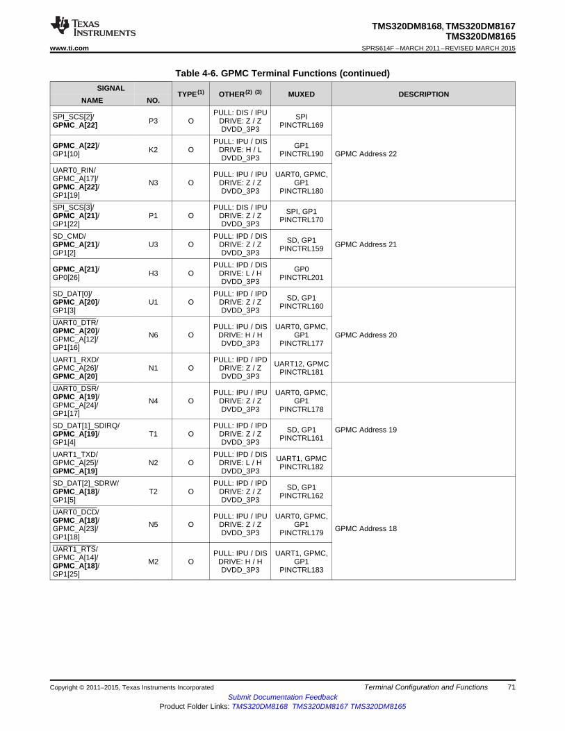
TMS320DM8168, TMS320DM8167TMS320DM8165
www.ti.com SPRS614F –MARCH 2011–REVISED MARCH 2015
Table 4-6. GPMC Terminal Functions (continued)SIGNAL
TYPE (1) OTHER (2) (3) MUXED DESCRIPTIONNAME NO.
PULL: DIS / IPUSPI_SCS[2]/ SPIP3 O DRIVE: Z / ZGPMC_A[22] PINCTRL169DVDD_3P3PULL: IPU / DISGPMC_A[22]/ GP1K2 O DRIVE: H / LGP1[10] PINCTRL190 GPMC Address 22DVDD_3P3
UART0_RIN/ PULL: IPU / IPU UART0, GPMC,GPMC_A[17]/ N3 O DRIVE: Z / Z GP1GPMC_A[22]/ DVDD_3P3 PINCTRL180GP1[19]SPI_SCS[3]/ PULL: DIS / IPU SPI, GP1GPMC_A[21]/ P1 O DRIVE: Z / Z PINCTRL170GP1[22] DVDD_3P3SD_CMD/ PULL: IPD / DIS SD, GP1GPMC_A[21]/ U3 O DRIVE: Z / Z GPMC Address 21PINCTRL159GP1[2] DVDD_3P3
PULL: IPD / DISGPMC_A[21]/ GP0H3 O DRIVE: L / HGP0[26] PINCTRL201DVDD_3P3SD_DAT[0]/ PULL: IPD / IPD SD, GP1GPMC_A[20]/ U1 O DRIVE: Z / Z PINCTRL160GP1[3] DVDD_3P3UART0_DTR/ PULL: IPU / DIS UART0, GPMC,GPMC_A[20]/ N6 O DRIVE: H / H GP1 GPMC Address 20GPMC_A[12]/ DVDD_3P3 PINCTRL177GP1[16]UART1_RXD/ PULL: IPD / IPD UART12, GPMCGPMC_A[26]/ N1 O DRIVE: Z / Z PINCTRL181GPMC_A[20] DVDD_3P3UART0_DSR/ PULL: IPU / IPU UART0, GPMC,GPMC_A[19]/ N4 O DRIVE: Z / Z GP1GPMC_A[24]/ DVDD_3P3 PINCTRL178GP1[17]SD_DAT[1]_SDIRQ/ PULL: IPD / IPD SD, GP1 GPMC Address 19GPMC_A[19]/ T1 O DRIVE: Z / Z PINCTRL161GP1[4] DVDD_3P3UART1_TXD/ PULL: IPD / DIS UART1, GPMCGPMC_A[25]/ N2 O DRIVE: L / H PINCTRL182GPMC_A[19] DVDD_3P3SD_DAT[2]_SDRW/ PULL: IPD / IPD SD, GP1GPMC_A[18]/ T2 O DRIVE: Z / Z PINCTRL162GP1[5] DVDD_3P3UART0_DCD/ PULL: IPU / IPU UART0, GPMC,GPMC_A[18]/ N5 O DRIVE: Z / Z GP1GPMC_A[23]/ GPMC Address 18DVDD_3P3 PINCTRL179GP1[18]UART1_RTS/ PULL: IPU / DIS UART1, GPMC,GPMC_A[14]/ M2 O DRIVE: H / H GP1GPMC_A[18]/ DVDD_3P3 PINCTRL183GP1[25]
Copyright © 2011–2015, Texas Instruments Incorporated Terminal Configuration and Functions 71Submit Documentation Feedback
Product Folder Links: TMS320DM8168 TMS320DM8167 TMS320DM8165
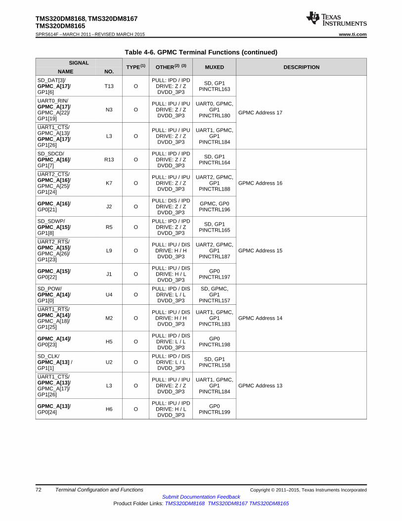
TMS320DM8168, TMS320DM8167TMS320DM8165SPRS614F –MARCH 2011–REVISED MARCH 2015 www.ti.com
Table 4-6. GPMC Terminal Functions (continued)SIGNAL
TYPE (1) OTHER (2) (3) MUXED DESCRIPTIONNAME NO.
SD_DAT[3]/ PULL: IPD / IPD SD, GP1GPMC_A[17]/ T13 O DRIVE: Z / Z PINCTRL163GP1[6] DVDD_3P3UART0_RIN/ PULL: IPU / IPU UART0, GPMC,GPMC_A[17]/ N3 O DRIVE: Z / Z GP1GPMC_A[22]/ GPMC Address 17DVDD_3P3 PINCTRL180GP1[19]UART1_CTS/ PULL: IPU / IPU UART1, GPMC,GPMC_A[13]/ L3 O DRIVE: Z / Z GP1GPMC_A[17]/ DVDD_3P3 PINCTRL184GP1[26]SD_SDCD/ PULL: IPD / IPD SD, GP1GPMC_A[16]/ R13 O DRIVE: Z / Z PINCTRL164GP1[7] DVDD_3P3UART2_CTS/ PULL: IPU / IPU UART2, GPMC,GPMC_A[16]/ K7 O DRIVE: Z / Z GP1 GPMC Address 16GPMC_A[25]/ DVDD_3P3 PINCTRL188GP1[24]
PULL: DIS / IPDGPMC_A[16]/ GPMC, GP0J2 O DRIVE: Z / ZGP0[21] PINCTRL196DVDD_3P3SD_SDWP/ PULL: IPD / IPD SD, GP1GPMC_A[15]/ R5 O DRIVE: Z / Z PINCTRL165GP1[8] DVDD_3P3UART2_RTS/ PULL: IPU / DIS UART2, GPMC,GPMC_A[15]/ L9 O DRIVE: H / H GP1 GPMC Address 15GPMC_A[26]/ DVDD_3P3 PINCTRL187GP1[23]
PULL: IPU / DISGPMC_A[15]/ GP0J1 O DRIVE: H / LGP0[22] PINCTRL197DVDD_3P3SD_POW/ PULL: IPD / DIS SD, GPMC,GPMC_A[14]/ U4 O DRIVE: L / L GP1GP1[0] DVDD_3P3 PINCTRL157UART1_RTS/ PULL: IPU / DIS UART1, GPMC,GPMC_A[14]/ M2 O DRIVE: H / H GP1 GPMC Address 14GPMC_A[18]/ DVDD_3P3 PINCTRL183GP1[25]
PULL: IPD / DISGPMC_A[14]/ GP0H5 O DRIVE: L / LGP0[23] PINCTRL198DVDD_3P3SD_CLK/ PULL: IPD / DIS SD, GP1GPMC_A[13] / U2 O DRIVE: L / L PINCTRL158GP1[1] DVDD_3P3UART1_CTS/ PULL: IPU / IPU UART1, GPMC,GPMC_A[13]/ L3 O DRIVE: Z / Z GP1 GPMC Address 13GPMC_A[17]/ DVDD_3P3 PINCTRL184GP1[26]
PULL: IPU / IPDGPMC_A[13]/ GP0H6 O DRIVE: H / LGP0[24] PINCTRL199DVDD_3P3
72 Terminal Configuration and Functions Copyright © 2011–2015, Texas Instruments IncorporatedSubmit Documentation Feedback
Product Folder Links: TMS320DM8168 TMS320DM8167 TMS320DM8165

TMS320DM8168, TMS320DM8167TMS320DM8165
www.ti.com SPRS614F –MARCH 2011–REVISED MARCH 2015
Table 4-6. GPMC Terminal Functions (continued)SIGNAL
TYPE (1) OTHER (2) (3) MUXED DESCRIPTIONNAME NO.
UART0_DTR/ PULL: IPU / DIS UART0, GPMC,GPMC_A[20]/ N6 O DRIVE: H / H GP1GPMC_A[12]/ DVDD_3P3 PINCTRL177GP1[16]PULL: IPD / DISGPMC_A[12]/ GP0H2 O DRIVE: L / HGP0[27] PINCTRL202DVDD_3P3 GPMC Address 12
TIM7_OUT/ PULL: IPD / IPD TIM7, GP0GPMC_A[12]/ G1 O DRIVE: L / L PINCTRL206GP0[31] DVDD_3P3PULL: IPU / IPUGPMC_CS[5]/ GPMCAG1 O DRIVE: H / HGPMC_A[12] PINCTRL212DVDD_3P3PULL: IPD / DISGPMC_A[11]/ GP0AC2 O DRIVE: Z / Z GPMC Address 11GP0[19] PINCTRL232DVDD_3P3PULL: IPD / DISGPMC_A[10]/ GP0AD1 O DRIVE: Z / Z GPMC Address 10GP0[18] PINCTRL231DVDD_3P3
GPMC_A[9]/ PULL: IPU / DIS GP0, BOOTGP0[17]/ AD2 O DRIVE: Z / Z GPMC Address 9PINCTRL230CS0WAIT DVDD_3P3GPMC_A[8]/ PULL: IPU / DIS GP0, BOOTGP0[16]/ AD4 O DRIVE: Z / Z GPMC Address 8PINCTRL229CS0BW DVDD_3P3GPMC_A[7]/ PULL: IPU / DIS GP0, BOOTGP0[15]/ AD3 O DRIVE: Z / Z GPMC Address 7PINCTRL228CS0MUX[1] DVDD_3P3GPMC_A[6]/ PULL: IPU / DIS GP0, BOOTGP0[14]/ AD8 O DRIVE: Z / Z GPMC Address 6PINCTRL227CS0MUX[0] DVDD_3P3GPMC_A[5]/ PULL: IPU / DIS GP0, BOOTGP0[13]/ AE2 O DRIVE: Z / Z GPMC Address 5PINCTRL226BTMODE[4] DVDD_3P3GPMC_A[4]/ PULL: IPU / DIS GP0, BOOTGP0[12]/ AE1 O DRIVE: Z / Z GPMC Address 4PINCTRL225BTMODE[3] DVDD_3P3GPMC_A[3]/ PULL: IPU / DIS GP0, BOOTGP0[11]/ AE3 O DRIVE: Z / Z GPMC Address 3PINCTRL224BTMODE[2] DVDD_3P3GPMC_A[2]/ PULL: IPU / DIS GP0, BOOTGP0[10]/ AE4 O DRIVE: Z / Z GPMC Address 2PINCTRL223BTMODE[1] DVDD_3P3GPMC_A[1]/ PULL: IPU / DIS GP0, BOOTGP0[9]/ AE5 O DRIVE: Z / Z GPMC Address 1PINCTRL222BTMODE[0] DVDD_3P3
PULL: IPD / DISGPMC_A[0]/ GP0AE6 O DRIVE: Z / Z GPMC Address 0GP0[8] PINCTRL221DVDD_3P3
Copyright © 2011–2015, Texas Instruments Incorporated Terminal Configuration and Functions 73Submit Documentation Feedback
Product Folder Links: TMS320DM8168 TMS320DM8167 TMS320DM8165
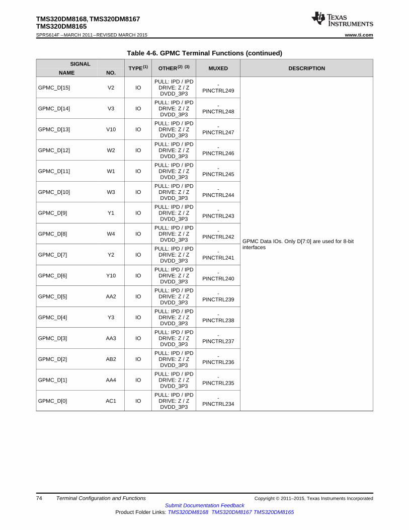
TMS320DM8168, TMS320DM8167TMS320DM8165SPRS614F –MARCH 2011–REVISED MARCH 2015 www.ti.com
Table 4-6. GPMC Terminal Functions (continued)SIGNAL
TYPE (1) OTHER (2) (3) MUXED DESCRIPTIONNAME NO.
PULL: IPD / IPD -GPMC_D[15] V2 IO DRIVE: Z / Z PINCTRL249DVDD_3P3PULL: IPD / IPD -GPMC_D[14] V3 IO DRIVE: Z / Z PINCTRL248DVDD_3P3PULL: IPD / IPD -GPMC_D[13] V10 IO DRIVE: Z / Z PINCTRL247DVDD_3P3PULL: IPD / IPD -GPMC_D[12] W2 IO DRIVE: Z / Z PINCTRL246DVDD_3P3PULL: IPD / IPD -GPMC_D[11] W1 IO DRIVE: Z / Z PINCTRL245DVDD_3P3PULL: IPD / IPD -GPMC_D[10] W3 IO DRIVE: Z / Z PINCTRL244DVDD_3P3PULL: IPD / IPD -GPMC_D[9] Y1 IO DRIVE: Z / Z PINCTRL243DVDD_3P3PULL: IPD / IPD -GPMC_D[8] W4 IO DRIVE: Z / Z PINCTRL242DVDD_3P3 GPMC Data IOs. Only D[7:0] are used for 8-bit
interfacesPULL: IPD / IPD -GPMC_D[7] Y2 IO DRIVE: Z / Z PINCTRL241DVDD_3P3PULL: IPD / IPD -GPMC_D[6] Y10 IO DRIVE: Z / Z PINCTRL240DVDD_3P3PULL: IPD / IPD -GPMC_D[5] AA2 IO DRIVE: Z / Z PINCTRL239DVDD_3P3PULL: IPD / IPD -GPMC_D[4] Y3 IO DRIVE: Z / Z PINCTRL238DVDD_3P3PULL: IPD / IPD -GPMC_D[3] AA3 IO DRIVE: Z / Z PINCTRL237DVDD_3P3PULL: IPD / IPD -GPMC_D[2] AB2 IO DRIVE: Z / Z PINCTRL236DVDD_3P3PULL: IPD / IPD -GPMC_D[1] AA4 IO DRIVE: Z / Z PINCTRL235DVDD_3P3PULL: IPD / IPD -GPMC_D[0] AC1 IO DRIVE: Z / Z PINCTRL234DVDD_3P3
74 Terminal Configuration and Functions Copyright © 2011–2015, Texas Instruments IncorporatedSubmit Documentation Feedback
Product Folder Links: TMS320DM8168 TMS320DM8167 TMS320DM8165

TMS320DM8168, TMS320DM8167TMS320DM8165
www.ti.com SPRS614F –MARCH 2011–REVISED MARCH 2015
4.2.6 High-Definition Multimedia Interface (HDMI) Signals
Table 4-7. HDMI Terminal FunctionsSIGNAL
TYPE (1) OTHER (2) (3) MUXED DESCRIPTIONNAME NO.
- HDMI Clock Output.HDMI_TMDSCLKP AT24 O -VDDA_HDMIWhen the HDMI PHY is powered down, these pins-HDMI_TMDSCLKN AU24 O - should be left unconnected.VDDA_HDMI
- HDMI Data 2 output.HDMI_TMDSDN2 AU27 O -VDDA_HDMIWhen the HDMI PHY is powered down, these pins-HDMI_TMDSDP2 AT27 O - should be left unconnected.VDDA_HDMI
- HDMI Data 1 output.HDMI_TMDSDN1 AU26 O -VDDA_HDMIWhen the HDMI PHY is powered down, these pins-HDMI_TMDSDP1 AT26 O - should be left unconnected.VDDA_HDMI
- HDMI Data 0 output.HDMI_TMDSDN0 AU25 O -VDDA_HDMIWhen the HDMI PHY is powered down, these pins-HDMI_TMDSDP0 AT25 O - should be left unconnected.VDDA_HDMI
PULL: DIS / DIS -HDMI_SCL AL25 O DRIVE: Z / Z HDMI I2C Serial Clock OutputPINCTRL301DVDD_3P3PULL: DIS / DIS -HDMI_SDA AK25 IO DRIVE: Z / Z HDMI I2C Serial Data IOPINCTRL302DVDD_3P3PULL: IPU / IPU -HDMI_CEC AP25 IO DRIVE: H / H HDMI Consumer Electronics Control IOPINCTRL303DVDD_3P3PULL: IPD / IPD HDMI Hot Plug Detect Input. Signals the-HDMI_HPDET AE24 I DRIVE: Z / Z connection / removal of an HDMI cable at thePINCTRL304DVDD_3P3 connector.
HDMI Voltage Reference. When HDMI is used,this pin must be connected via an external 6.8K-Ω(±1% tolerance) resistor to VSS.HDMI_EXTSWING AN25 A - -When the HDMI PHY is powered down, this pinshould be left unconnected.
(1) I = Input, O = Output, Z = High impedance, S = Supply voltage, GND = Ground, A = Analog signal.(2) PULL: A / B, where:
A is the state of the internal pull resistor during POR resetB is the state of the internal pull resistor after POR and Warm reset are de-asserted and during Warm resetIPD = Internal Pulldown Enabled, IPU = Internal Pullup Enabled, DIS = Internal Pull DisabledDRIVE: A / B, where;A is the driving state of the pin during POR resetB is the driving state of the pin after POR and Warm reset are de-asserted and during Warm resetH = Driving High, L = Driving Low, Z = 3-StateFor more detailed information on pullup and pulldown resistors and situations where external pullup and pulldown resistors are required,see Section 6.3.1, Pullup and Pulldown Resistors.
(3) Specifies the operating IO supply voltage for each signal.
Copyright © 2011–2015, Texas Instruments Incorporated Terminal Configuration and Functions 75Submit Documentation Feedback
Product Folder Links: TMS320DM8168 TMS320DM8167 TMS320DM8165

TMS320DM8168, TMS320DM8167TMS320DM8165SPRS614F –MARCH 2011–REVISED MARCH 2015 www.ti.com
4.2.7 Inter-Integrated Circuit (I2C) Signals
Table 4-8. I2C Terminal FunctionsSIGNAL
TYPE (1) OTHER (2) (3) MUXED DESCRIPTIONNAME NO.
I2C0PULL: DIS / DIS -I2C[0]_SCL N32 IO DRIVE: Z / Z I2C0 Clock IOPINCTRL287DVDD_3P3PULL: DIS / DIS -I2C[0]_SDA N33 IO DRIVE: Z / Z I2C0 Data IOPINCTRL288DVDD_3P3
I2C1PULL: DIS / DIS -I2C[1]_SCL N34 IO DRIVE: Z / Z I2C1 Clock IOPINCTRL289DVDD_3P3PULL: DIS / DIS -I2C[1]_SDA N35 IO DRIVE: Z / Z I2C1 Data IOPINCTRL290DVDD_3P3
(1) I = Input, O = Output, Z = High impedance, S = Supply voltage, GND = Ground, A = Analog signal.(2) PULL: A / B, where:
A is the state of the internal pull resistor during POR resetB is the state of the internal pull resistor after POR and Warm reset are de-asserted and during Warm resetIPD = Internal Pulldown Enabled, IPU = Internal Pullup Enabled, DIS = Internal Pull DisabledDRIVE: A / B, where;A is the driving state of the pin during POR resetB is the driving state of the pin after POR and Warm reset are de-asserted and during Warm resetH = Driving High, L = Driving Low, Z = 3-StateFor more detailed information on pullup and pulldown resistors and situations where external pullup and pulldown resistors are required,see Section 6.3.1, Pullup and Pulldown Resistors.
(3) Specifies the operating IO supply voltage for each signal.
76 Terminal Configuration and Functions Copyright © 2011–2015, Texas Instruments IncorporatedSubmit Documentation Feedback
Product Folder Links: TMS320DM8168 TMS320DM8167 TMS320DM8165

TMS320DM8168, TMS320DM8167TMS320DM8165
www.ti.com SPRS614F –MARCH 2011–REVISED MARCH 2015
4.2.8 Multichannel Audio Serial Port Signals
Table 4-9. McASP0 Terminal FunctionsSIGNAL
TYPE (1) OTHER (2) (3) MUXED DESCRIPTIONNAME NO.
PULL: IPD / IPD -MCA[0]_ACLKR AK28 IO DRIVE: Z / Z McASP0 Receive Bit Clock IOPINCTRL126DVDD_3P3PULL: IPD / IPD -MCA[0]_AHCLKR AJ27 IO DRIVE: Z / Z McASP0 Receive High-Frequency Master Clock IOPINCTRL127DVDD_3P3PULL: IPD / IPD -MCA[0]_AFSR AG29 IO DRIVE: Z / Z McASP0 Receive Frame Sync IOPINCTRL128DVDD_3P3PULL: IPD / IPDGP0[7]/ GP0H35 IO DRIVE: Z / Z McASP0 Mute InputMCA[0]_AMUTEIN PINCTRL298DVDD_3P3PULL: IPD / IPD -MCA[0]_ACLKX AH30 IO DRIVE: Z / Z McASP0 Transmit Bit Clock IOPINCTRL129DVDD_3P3PULL: IPD / IPD -MCA[0]_AHCLKX AH31 IO DRIVE: Z / Z McASP0 Transmit High-Frequency Master Clock IOPINCTRL130DVDD_3P3PULL: IPD / IPD -MCA[0]_AFSX AJ31 IO DRIVE: Z / Z McASP0 Transmit Frame Sync IOPINCTRL131DVDD_3P3PULL: IPD / IPD -MCA[0]_AMUTE AJ35 O DRIVE: Z / Z McASP0 Mute OutputPINCTRL132DVDD_3P3PULL: IPD / IPDMCA[0]_AXR[5]/ MCBAJ37 IO DRIVE: Z / ZMCB_DR PINCTRL138DVDD_3P3PULL: IPD / IPDMCA[0]_AXR[4]/ MCBAJ36 IO DRIVE: Z / ZMCB_DX PINCTRL137DVDD_3P3PULL: IPD / IPDMCA[0]_AXR[3]/ MCBAJ34 IO DRIVE: Z / ZMCB_FSR PINCTRL136DVDD_3P3
McASP0 Transmit/Receive Data IOsPULL: IPD / IPDMCA[0]_AXR[2]/ MCBAJ33 IO DRIVE: Z / ZMCB_FSX PINCTRL135DVDD_3P3PULL: IPD / IPD -MCA[0]_AXR[1] AJ32 IO DRIVE: Z / Z PINCTRL134DVDD_3P3PULL: IPD / IPD -MCA[0]_AXR[0] AK37 IO DRIVE: Z / Z PINCTRL133DVDD_3P3
(1) I = Input, O = Output, Z = High impedance, S = Supply voltage, GND = Ground, A = Analog signal.(2) PULL: A / B, where:
A is the state of the internal pull resistor during POR resetB is the state of the internal pull resistor after POR and Warm reset are de-asserted and during Warm resetIPD = Internal Pulldown Enabled, IPU = Internal Pullup Enabled, DIS = Internal Pull DisabledDRIVE: A / B, where;A is the driving state of the pin during POR resetB is the driving state of the pin after POR and Warm reset are de-asserted and during Warm resetH = Driving High, L = Driving Low, Z = 3-StateFor more detailed information on pullup and pulldown resistors and situations where external pullup and pulldown resistors are required,see Section 6.3.1, Pullup and Pulldown Resistors.
(3) Specifies the operating IO supply voltage for each signal.
Copyright © 2011–2015, Texas Instruments Incorporated Terminal Configuration and Functions 77Submit Documentation Feedback
Product Folder Links: TMS320DM8168 TMS320DM8167 TMS320DM8165

TMS320DM8168, TMS320DM8167TMS320DM8165SPRS614F –MARCH 2011–REVISED MARCH 2015 www.ti.com
Table 4-10. McASP1 Terminal FunctionsSIGNAL
TYPE (1) OTHER (2) (3) MUXED DESCRIPTIONNAME NO.
PULL: IPD / IPD -MCA[1]_ACLKR AK36 IO DRIVE: Z / Z McASP1 Receive Bit Clock IOPINCTRL139DVDD_3P3PULL: IPD / IPD -MCA[1]_AHCLKR AL37 IO DRIVE: Z / Z McASP1 Receive High-Frequency Master Clock IOPINCTRL140DVDD_3P3PULL: IPD / IPD -MCA[1]_AFSR AK35 IO DRIVE: Z / Z McASP1 Receive Frame Sync IOPINCTRL141DVDD_3P3
GP0[6]/ PULL: IPD / IPD GP0, GPMCMCA[1]_AMUTEIN/ G5 I DRIVE: Z / Z McASP1 Mute InputPINCTRL297GPMC_A[23] DVDD_3P3PULL: IPD / IPD -MCA[1]_ACLKX AL36 IO DRIVE: Z / Z McASP1 Transmit Bit Clock IOPINCTRL142DVDD_3P3PULL: IPD / IPD -MCA[1]_AHCLKX AM37 IO DRIVE: Z / Z McASP1 Transmit High-Frequency Master Clock IOPINCTRL143DVDD_3P3PULL: IPD / IPD -MCA[1]_AFSX AK34 IO DRIVE: Z / Z McASP1 Transmit Frame Sync IOPINCTRL144DVDD_3P3PULL: IPD / IPD -MCA[1]_AMUTE AK33 O DRIVE: Z / Z McASP1 Mute OutputPINCTRL145DVDD_3P3PULL: IPD / IPD -MCA[1]_AXR[1] AK32 IO DRIVE: Z / Z PINCTRL147DVDD_3P3
McASP1 Transmit/Receive Data IOsPULL: IPD / IPD -MCA[1]_AXR[0] AL33 IO DRIVE: Z / Z PINCTRL146DVDD_3P3
(1) I = Input, O = Output, Z = High impedance, S = Supply voltage, GND = Ground, A = Analog signal.(2) PULL: A / B, where:
A is the state of the internal pull resistor during POR resetB is the state of the internal pull resistor after POR and Warm reset are de-asserted and during Warm resetIPD = Internal Pulldown Enabled, IPU = Internal Pullup Enabled, DIS = Internal Pull DisabledDRIVE: A / B, where;A is the driving state of the pin during POR resetB is the driving state of the pin after POR and Warm reset are de-asserted and during Warm resetH = Driving High, L = Driving Low, Z = 3-StateFor more detailed information on pullup and pulldown resistors and situations where external pullup and pulldown resistors are required,see Section 6.3.1, Pullup and Pulldown Resistors.
(3) Specifies the operating IO supply voltage for each signal.
78 Terminal Configuration and Functions Copyright © 2011–2015, Texas Instruments IncorporatedSubmit Documentation Feedback
Product Folder Links: TMS320DM8168 TMS320DM8167 TMS320DM8165

TMS320DM8168, TMS320DM8167TMS320DM8165
www.ti.com SPRS614F –MARCH 2011–REVISED MARCH 2015
Table 4-11. McASP2 Terminal FunctionsSIGNAL
TYPE (1) OTHER (2) (3) MUXED DESCRIPTIONNAME NO.
MCA[2]_ACLKR/ PULL: IPD / IPD MCBMCB_CLKR/ AL34 IO DRIVE: Z / Z McASP2 Receive Bit Clock IOPINCTRL148MCB_DR DVDD_3P3PULL: IPD / IPDMCA[2]_AHCLKR/ MCBAM34 IO DRIVE: Z / Z McASP2 Receive High-Frequency Master Clock IOMCB_CLKS PINCTRL149DVDD_3P3
MCA[2]_AFSR/ PULL: IPD / IPD MCBMCB_CLKX/ AM35 IO DRIVE: Z / Z McASP2 Receive Frame Sync IOPINCTRL150MCB_FSR DVDD_3P3GP0[5]/ PULL: IPD / IPD GP0, GPMCMCA[2]_AMUTEIN/ G2 I DRIVE: Z / Z McASP2 Mute InputPINCTRL296GPMC_A[24] DVDD_3P3
PULL: IPD / IPDMCA[2]_ACLKX/ MCBAM36 IO DRIVE: Z / Z McASP2 Transmit Bit Clock IOMCB_CLKX PINCTRL151DVDD_3P3PULL: IPD / IPDMCA[2]_AHCLKX/ MCBAN36 IO DRIVE: Z / Z McASP2 Transmit High-Frequency Master Clock IOMCB_CLKR PINCTRL152DVDD_3P3
MCA[2]_AFSX/ PULL: IPD / IPD MCBMCB_CLKS/ AN35 IO DRIVE: Z / Z McASP2 Transmit Frame Sync IOPINCTRL153MCB_FSX DVDD_3P3PULL: IPD / IPD -MCA[2]_AMUTE AP36 O DRIVE: Z / Z McASP2 Mute OutputPINCTRL154DVDD_3P3PULL: IPD / IPDMCA[2]_AXR[1]/ MCBAR37 IO DRIVE: Z / ZMCB_DX PINCTRL156DVDD_3P3
McASP2 Transmit/Receive Data IOsPULL: IPD / IPD -MCA[2]_AXR[0] AR36 IO DRIVE: Z / Z PINCTRL155DVDD_3P3
(1) I = Input, O = Output, Z = High impedance, S = Supply voltage, GND = Ground, A = Analog signal.(2) PULL: A / B, where:
A is the state of the internal pull resistor during POR resetB is the state of the internal pull resistor after POR and Warm reset are de-asserted and during Warm resetIPD = Internal Pulldown Enabled, IPU = Internal Pullup Enabled, DIS = Internal Pull DisabledDRIVE: A / B, where;A is the driving state of the pin during POR resetB is the driving state of the pin after POR and Warm reset are de-asserted and during Warm resetH = Driving High, L = Driving Low, Z = 3-StateFor more detailed information on pullup and pulldown resistors and situations where external pullup and pulldown resistors are required,see Section 6.3.1, Pullup and Pulldown Resistors.
(3) Specifies the operating IO supply voltage for each signal.
Copyright © 2011–2015, Texas Instruments Incorporated Terminal Configuration and Functions 79Submit Documentation Feedback
Product Folder Links: TMS320DM8168 TMS320DM8167 TMS320DM8165

TMS320DM8168, TMS320DM8167TMS320DM8165SPRS614F –MARCH 2011–REVISED MARCH 2015 www.ti.com
4.2.9 Multichannel Buffered Serial Port Signals
Table 4-12. McBSP Terminal FunctionsSIGNAL
TYPE (1) OTHER (2) (3) MUXED DESCRIPTIONNAME NO.
MCA[2]_ACLKR/ PULL: IPD / IPD MCA[2], MCBMCB_CLKR/ AL34 IO DRIVE: Z / Z PINCTRL148MCB_DR DVDD_3P3McBSP Receive Clock IO
PULL: IPD / IPDMCA[2]_AHCLKX/ MCA[2]AN36 IO DRIVE: Z / ZMCB_CLKR PINCTRL152DVDD_3P3PULL: IPD / IPDMCA[0]_AXR[3]/ MCA[0]AJ34 IO DRIVE: Z / ZMCB_FSR PINCTRL136DVDD_3P3
McBSP Receive Frame Sync IOMCA[2]_AFSR/ PULL: IPD / IPD MCA[2], MCBMCB_CLKX/ AM35 IO DRIVE: Z / Z PINCTRL150MCB_FSR DVDD_3P3
PULL: IPD / IPDMCA[0]_AXR[5]/ MCA[0]AJ37 I DRIVE: Z / ZMCB_DR PINCTRL138DVDD_3P3McBSP Receive Data Input
MCA[2]_ACLKR/ PULL: IPD / IPD MCA[2], MCBMCB_CLKR/ AL34 I DRIVE: Z / Z PINCTRL148MCB_DR DVDD_3P3MCA[2]_AFSR/ PULL: IPD / IPD MCA[2], MCBMCB_CLKX/ AM35 IO DRIVE: Z / Z PINCTRL150MCB_FSR DVDD_3P3
McBSP Transmit Clock IOPULL: IPD / IPDMCA[2]_ACLKX/ MCA[2]AM36 IO DRIVE: Z / ZMCB_CLKX PINCTRL151DVDD_3P3PULL: IPD / IPDMCA[0]_AXR[2]/ MCA[0]AJ33 IO DRIVE: Z / ZMCB_FSX PINCTRL135DVDD_3P3
McBSP Transmit Frame Sync IOMCA[2]_AFSX/ PULL: IPD / IPD MCA[2], MCBMCB_CLKS/ AN35 IO DRIVE: Z / Z PINCTRL153MCB_FSX DVDD_3P3
PULL: IPD / IPDMCA[0]_AXR[4]/ MCA[0]AJ36 O DRIVE: Z / ZMCB_DX PINCTRL137DVDD_3P3McBSP Transmit Data Output
PULL: IPD / IPDMCA[2]_AXR[1]/ MCA[2]AR37 O DRIVE: Z / ZMCB_DX PINCTRL156DVDD_3P3PULL: IPD / IPDMCA[2]_AHCLKR/ MCA[2]AM34 I DRIVE: Z / ZMCB_CLKS PINCTRL149DVDD_3P3
McBSP Source Clock InputMCA[2]_AFSX/ PULL: IPD / IPD MCA[2], MCBMCB_CLKS/ AN35 I DRIVE: Z / Z PINCTRL153MCB_FSX DVDD_3P3
(1) I = Input, O = Output, Z = High impedance, S = Supply voltage, GND = Ground, A = Analog signal.(2) PULL: A / B, where:
A is the state of the internal pull resistor during POR resetB is the state of the internal pull resistor after POR and Warm reset are de-asserted and during Warm resetIPD = Internal Pulldown Enabled, IPU = Internal Pullup Enabled, DIS = Internal Pull DisabledDRIVE: A / B, where;A is the driving state of the pin during POR resetB is the driving state of the pin after POR and Warm reset are de-asserted and during Warm resetH = Driving High, L = Driving Low, Z = 3-StateFor more detailed information on pullup and pulldown resistors and situations where external pullup and pulldown resistors are required,see Section 6.3.1, Pullup and Pulldown Resistors.
(3) Specifies the operating IO supply voltage for each signal.
80 Terminal Configuration and Functions Copyright © 2011–2015, Texas Instruments IncorporatedSubmit Documentation Feedback
Product Folder Links: TMS320DM8168 TMS320DM8167 TMS320DM8165

TMS320DM8168, TMS320DM8167TMS320DM8165
www.ti.com SPRS614F –MARCH 2011–REVISED MARCH 2015
4.2.10 Oscillator/Phase-Locked Loop (PLL) Signals
Table 4-13. Oscillator/PLL and Clock Generator Terminal FunctionsSIGNAL
TYPE (1) OTHER (2) (3) MUXED DESCRIPTIONNAME NO.
CLOCK GENERATORPULL: IPU / DIS - Device Clock output. Can be used as a system clockCLKOUT F1 O DRIVE: L / L PINCTRL320 for other devicesDVDD_3P3
OSCILLATOR/PLLDevice Crystal input. Crystal connection to internalDEV_MXI/ DISA19 I - oscillator for system clock. Functions as CLKINDEVDEV_CLKIN DEV_DVDD18 clock input when an external oscillator is used.Device Crystal output. Crystal connection to internalDISDEV_MXO C19 O - oscillator for system clock. When device oscillator isDEV_DVDD18 BYPASSED, leave this pin unconnected.1.8 V Power Supply for Device (DEV) Oscillator. If the
DEVOSC_DVDD18 E19 S - - internal oscillator is bypassed, DEVOSC_DVDD18should still be connected to the 1.8-V power supply.Supply Ground for DEV Oscillator. If the internal
DEVOSC_VSS B19 GND - - oscillator is bypassed, DEVOSC_VSS should beconnected to ground (VSS).
PULL: IPU / IPD - RTC Clock input. Optional 32.768 kHz clock for RTCCLKIN32 H37 I DRIVE: Z / Z PINCTRL321 reference. If this pin is not used, it should be held low.DVDD_3P3
(1) I = Input, O = Output, Z = High impedance, S = Supply voltage, GND = Ground, A = Analog signal.(2) PULL: A / B, where:
A is the state of the internal pull resistor during POR resetB is the state of the internal pull resistor after POR and Warm reset are de-asserted and during Warm resetIPD = Internal Pulldown Enabled, IPU = Internal Pullup Enabled, DIS = Internal Pull DisabledDRIVE: A / B, where;A is the driving state of the pin during POR resetB is the driving state of the pin after POR and Warm reset are de-asserted and during Warm resetH = Driving High, L = Driving Low, Z = 3-StateFor more detailed information on pullup and pulldown resistors and situations where external pullup and pulldown resistors are required,see Section 6.3.1, Pullup and Pulldown Resistors.
(3) Specifies the operating IO supply voltage for each signal.
Copyright © 2011–2015, Texas Instruments Incorporated Terminal Configuration and Functions 81Submit Documentation Feedback
Product Folder Links: TMS320DM8168 TMS320DM8167 TMS320DM8165
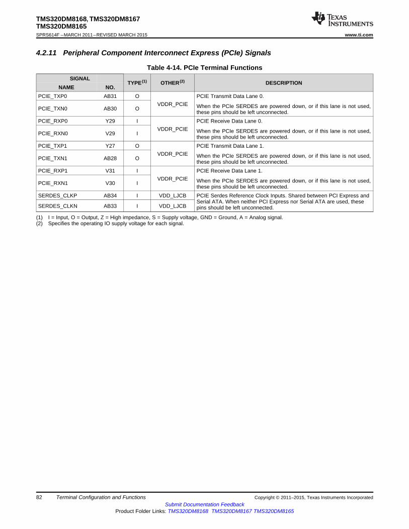
TMS320DM8168, TMS320DM8167TMS320DM8165SPRS614F –MARCH 2011–REVISED MARCH 2015 www.ti.com
4.2.11 Peripheral Component Interconnect Express (PCIe) Signals
Table 4-14. PCIe Terminal FunctionsSIGNAL
TYPE (1) OTHER (2) DESCRIPTIONNAME NO.
PCIE_TXP0 AB31 O PCIE Transmit Data Lane 0.VDDR_PCIE When the PCIe SERDES are powered down, or if this lane is not used,PCIE_TXN0 AB30 O
these pins should be left unconnected.PCIE_RXP0 Y29 I PCIE Receive Data Lane 0.
VDDR_PCIE When the PCIe SERDES are powered down, or if this lane is not used,PCIE_RXN0 V29 Ithese pins should be left unconnected.
PCIE_TXP1 Y27 O PCIE Transmit Data Lane 1.VDDR_PCIE When the PCIe SERDES are powered down, or if this lane is not used,PCIE_TXN1 AB28 O
these pins should be left unconnected.PCIE_RXP1 V31 I PCIE Receive Data Lane 1.
VDDR_PCIE When the PCIe SERDES are powered down, or if this lane is not used,PCIE_RXN1 V30 Ithese pins should be left unconnected.
SERDES_CLKP AB34 I VDD_LJCB PCIE Serdes Reference Clock Inputs. Shared between PCI Express andSerial ATA. When neither PCI Express nor Serial ATA are used, these
SERDES_CLKN AB33 I VDD_LJCB pins should be left unconnected.
(1) I = Input, O = Output, Z = High impedance, S = Supply voltage, GND = Ground, A = Analog signal.(2) Specifies the operating IO supply voltage for each signal.
82 Terminal Configuration and Functions Copyright © 2011–2015, Texas Instruments IncorporatedSubmit Documentation Feedback
Product Folder Links: TMS320DM8168 TMS320DM8167 TMS320DM8165

TMS320DM8168, TMS320DM8167TMS320DM8165
www.ti.com SPRS614F –MARCH 2011–REVISED MARCH 2015
4.2.12 Reset, Interrupts, and JTAG Interface Signals
Table 4-15. RESET, Interrupts, and JTAG Terminal FunctionsSIGNAL
TYPE (1) OTHER (2) (3) MUXED DESCRIPTIONNAME NO.
RESETPULL: IPD / IPU -RESET G33 I DRIVE: Z / Z Device Reset inputPINCTRL316DVDD_3P3
IPUPOR F37 I - Power-On Reset inputDVDD_3P3Reset outputPULL: DIS / DIS -RSTOUT G37 O For more detailed information on RSTOUT pinDVDD_3P3 PINCTRL318 behavior, see Section 8.2.13
INTERRUPTSPULL: IPD / IPU -NMI G36 I DRIVE: Z / Z External active low maskable interruptPINCTRL317DVDD_3P3
Interrupt-capable general-purpose IOsNOTE: All pins are multiplexed with other pinseeGP0[31:3] IO see NOTE - functions. For muxing and internal pullup, pulldown,Table 4-5 or disable details, see Table 4-5, GPIO TerminalFunctions.Interrupt-capable general-purpose IOsNOTE: All pins are multiplexed with other pinseeGP1[31:0] IO see NOTE - functions. For muxing and internal pullup, pulldown,Table 4-5 or disable details, see Table 4-5, GPIO TerminalFunctions.
JTAGPULL: IPU / IPU -TCLK J37 I DRIVE: H / H JTAG test clock inputPINCTRL305DVDD_3P3PULL: IPD / DIS -RTCK J36 O DRIVE: L / H JTAG return clock outputPINCTRL306DVDD_3P3PULL: IPU / IPU -TDI J34 I DRIVE: H / H JTAG test data inputPINCTRL307DVDD_3P3PULL: IPD / DIS -TDO N30 O DRIVE: Z / Z JTAG test port data outputPINCTRL308DVDD_3P3PULL: IPU / IPU - JTAG test port mode select input. For properTMS N31 I DRIVE: Z / Z PINCTRL309 operation, do not oppose the IPU on this pin.DVDD_3P3PULL: IPD / IPD -TRST K36 I DRIVE: L / L JTAG test port reset inputPINCTRL310DVDD_3P3PULL: IPU / IPU -EMU4 M37 IO DRIVE: Z / Z Emulator pin 4PINCTRL315DVDD_3P3
(1) I = Input, O = Output, Z = High impedance, S = Supply voltage, GND = Ground, A = Analog signal.(2) PULL: A / B, where:
A is the state of the internal pull resistor during POR resetB is the state of the internal pull resistor after POR and Warm reset are de-asserted and during Warm resetIPD = Internal Pulldown Enabled, IPU = Internal Pullup Enabled, DIS = Internal Pull DisabledDRIVE: A / B, where;A is the driving state of the pin during POR resetB is the driving state of the pin after POR and Warm reset are de-asserted and during Warm resetH = Driving High, L = Driving Low, Z = 3-StateFor more detailed information on pullup and pulldown resistors and situations where external pullup and pulldown resistors are required,see Section 6.3.1, Pullup and Pulldown Resistors.
(3) Specifies the operating IO supply voltage for each signal.
Copyright © 2011–2015, Texas Instruments Incorporated Terminal Configuration and Functions 83Submit Documentation Feedback
Product Folder Links: TMS320DM8168 TMS320DM8167 TMS320DM8165

TMS320DM8168, TMS320DM8167TMS320DM8165SPRS614F –MARCH 2011–REVISED MARCH 2015 www.ti.com
Table 4-15. RESET, Interrupts, and JTAG Terminal Functions (continued)SIGNAL
TYPE (1) OTHER (2) (3) MUXED DESCRIPTIONNAME NO.
PULL: IPU / IPU -EMU3 M36 IO DRIVE: Z / Z Emulator pin 3PINCTRL314DVDD_3P3PULL: IPU / IPU -EMU2 L37 IO DRIVE: Z / Z Emulator pin 2PINCTRL313DVDD_3P3PULL: IPU / IPU -EMU1 L36 IO DRIVE: Z / Z Emulator pin 1PINCTRL312DVDD_3P3PULL: IPU / IPU -EMU0 J35 IO DRIVE: Z / Z Emulator pin 0PINCTRL311DVDD_3P3
84 Terminal Configuration and Functions Copyright © 2011–2015, Texas Instruments IncorporatedSubmit Documentation Feedback
Product Folder Links: TMS320DM8168 TMS320DM8167 TMS320DM8165
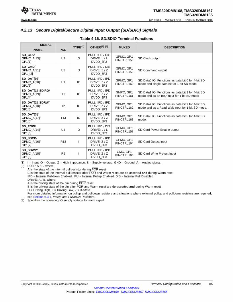
TMS320DM8168, TMS320DM8167TMS320DM8165
www.ti.com SPRS614F –MARCH 2011–REVISED MARCH 2015
4.2.13 Secure Digital/Secure Digital Input Output (SD/SDIO) Signals
Table 4-16. SD/SDIO Terminal FunctionsSIGNAL
TYPE (1) OTHER (2) (3) MUXED DESCRIPTIONNAME NO.
SD_CLK/ PULL: IPD / DIS GPMC, GP1GPMC_A[13]/ U2 O DRIVE: L / L SD Clock outputPINCTRL158GP1[1] DVDD_3P3SD_CMD/ PULL: IPD / DIS GPMC, GP1GPMC_A[21]/ U3 O DRIVE: Z / Z SD Command outputPINCTRL159GP1_[2] DVDD_3P3SD_DAT[0]/ PULL: IPD / IPD GPMC, GP1 SD Data0 IO. Functions as data bit 0 for 4-bit SDGPMC_A[20]/ U1 IO DRIVE: Z / Z PINCTRL160 mode and single data bit for 1-bit SD mode.GP1[3] DVDD_3P3SD_DAT[1]_SDIRQ/ PULL: IPD / IPD GMPC, GP1 SD Data1 IO. Functions as data bit 1 for 4-bit SDGPMC_A[19]/ T1 IO DRIVE: Z / Z PINCTRL161 mode and as an IRQ input for 1-bit SD modeGP1[4] DVDD_3P3SD_DAT[2]_SDRW/ PULL: IPD / IPD GPMC, GP1 SD Data2 IO. Functions as data bit 2 for 4-bit SDGPMC_A[18]/ T2 IO DRIVE: Z / Z PINCTRL162 mode and as a Read Wait input for 1-bit SD mode.GP1[5] DVDD_3P3SD_DAT[3]/ PULL: IPD / IPD GPMC, GP1 SD Data3 IO. Functions as data bit 3 for 4-bit SDGPMC_A[17]/ T13 IO DRIVE: Z / Z PINCTRL163 mode.GP1[6] DVDD_3P3SD_POW/ PULL: IPD / DIS GPMC, GP1GPMC_A[14]/ U4 O DRIVE: L / L SD Card Power Enable outputPINCTRL157GP1[0] DVDD_3P3SD_SDCD/ PULL: IPD / IPD GPMC, GP1GPMC_A[16]/ R13 I DRIVE: Z / Z SD Card Detect inputPINCTRL164GP1[7] DVDD_3P3SD_SDWP/ PULL: IPD / IPD GMC, GP1GPMC_A[15]/ R5 I DRIVE: Z / Z SD Card Write Protect inputPINCTRL165GP1[8] DVDD_3P3
(1) I = Input, O = Output, Z = High impedance, S = Supply voltage, GND = Ground, A = Analog signal.(2) PULL: A / B, where:
A is the state of the internal pull resistor during POR resetB is the state of the internal pull resistor after POR and Warm reset are de-asserted and during Warm resetIPD = Internal Pulldown Enabled, IPU = Internal Pullup Enabled, DIS = Internal Pull DisabledDRIVE: A / B, where;A is the driving state of the pin during POR resetB is the driving state of the pin after POR and Warm reset are de-asserted and during Warm resetH = Driving High, L = Driving Low, Z = 3-StateFor more detailed information on pullup and pulldown resistors and situations where external pullup and pulldown resistors are required,see Section 6.3.1, Pullup and Pulldown Resistors.
(3) Specifies the operating IO supply voltage for each signal.
Copyright © 2011–2015, Texas Instruments Incorporated Terminal Configuration and Functions 85Submit Documentation Feedback
Product Folder Links: TMS320DM8168 TMS320DM8167 TMS320DM8165

TMS320DM8168, TMS320DM8167TMS320DM8165SPRS614F –MARCH 2011–REVISED MARCH 2015 www.ti.com
4.2.14 Serial ATA Signals
NOTESerial ATA pins J32 and J33 have a different naming convention and functionality for siliconrevision 1.x devices and silicon revision 2.x devices. These pins are listed separately inTable 4-18.
Table 4-17. Serial ATA Terminal FunctionsSIGNAL
TYPE (1) OTHER (2) (3) MUXED DESCRIPTIONNAME NO.
- Serial ATA Data Transmit for disk 0.SATA_TXN0 T31 O -VDDR_SATAWhen the SATA SERDES are powered down, these-SATA_TXP0 T32 O - pins should be left unconnected.VDDR_SATA
- Serial ATA Data Transmit for disk 1.SATA_TXN1 U33 O -VDDR_SATAWhen the SATA SERDES are powered down, these-SATA_TXP1 V33 O - pins should be left unconnected.VDDR_SATA
- Serial ATA Data Receive for disk 0.SATA_RXN0 V37 I -VDDR_SATAWhen the SATA SERDES are powered down, these-SATA_RXP0 V36 I - pins should be left unconnected.VDDR_SATA
- Serial ATA Data Receive for disk 1.SATA_RXN1 V35 I -VDDR_SATAWhen the SATA SERDES are powered down, these-SATA_RXP1 W35 I - pins should be left unconnected.VDDR_SATA
-SERDES_CLKP AB34 I -VDD_LJCB PCIE Serdes Reference Clock Input. Shared betweenPCI Express and Serial ATA.-SERDES_CLKN AB33 I -VDD_LJCB
(1) I = Input, O = Output, Z = High impedance, S = Supply voltage, GND = Ground, A = Analog signal.(2) PULL: A / B, where:
A is the state of the internal pull resistor during POR resetB is the state of the internal pull resistor after POR and Warm reset are de-asserted and during Warm resetIPD = Internal Pulldown Enabled, IPU = Internal Pullup Enabled, DIS = Internal Pull DisabledDRIVE: A / B, where;A is the driving state of the pin during POR resetB is the driving state of the pin after POR and Warm reset are de-asserted and during Warm resetH = Driving High, L = Driving Low, Z = 3-StateFor more detailed information on pullup and pulldown resistors and situations where external pullup and pulldown resistors are required,see Section 6.3.1, Pullup and Pulldown Resistors.
(3) Specifies the operating IO supply voltage for each signal.
Table 4-18. Serial ATA [Pins J32, J33] Terminal FunctionsSIGNAL
TYPE (1) OTHER (2) (3) MUXED DESCRIPTIONNAME NO.
Silicon Revision 1.x
(1) I = Input, O = Output, Z = High impedance, S = Supply voltage, GND = Ground, A = Analog signal.(2) PULL: A / B, where:
A is the state of the internal pull resistor during POR resetB is the state of the internal pull resistor after POR and Warm reset are de-asserted and during Warm resetIPD = Internal Pulldown Enabled, IPU = Internal Pullup Enabled, DIS = Internal Pull DisabledDRIVE: A / B, where;A is the driving state of the pin during POR resetB is the driving state of the pin after POR and Warm reset are de-asserted and during Warm resetH = Driving High, L = Driving Low, Z = 3-StateFor more detailed information on pullup and pulldown resistors and situations where external pullup and pulldown resistors are required,see Section 6.3.1, Pullup and Pulldown Resistors.
(3) Specifies the operating IO supply voltage for each signal.
86 Terminal Configuration and Functions Copyright © 2011–2015, Texas Instruments IncorporatedSubmit Documentation Feedback
Product Folder Links: TMS320DM8168 TMS320DM8167 TMS320DM8165
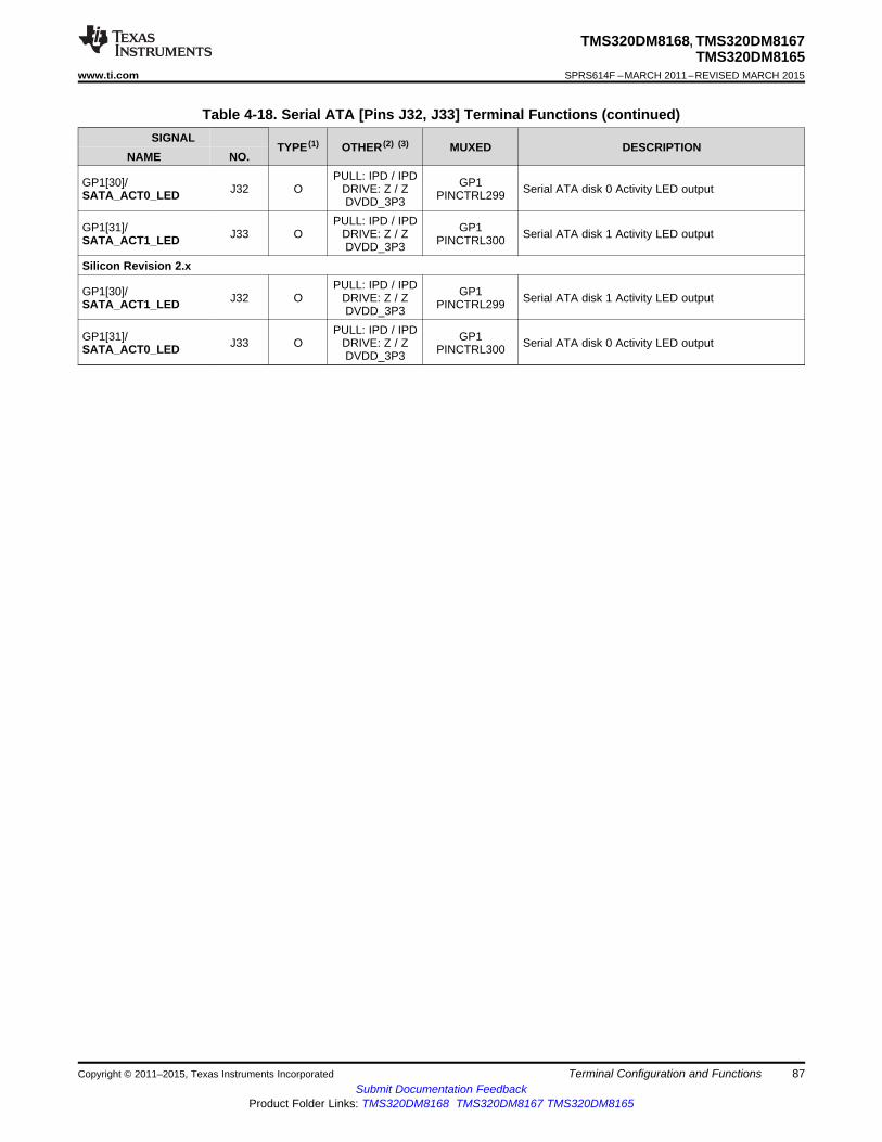
TMS320DM8168, TMS320DM8167TMS320DM8165
www.ti.com SPRS614F –MARCH 2011–REVISED MARCH 2015
Table 4-18. Serial ATA [Pins J32, J33] Terminal Functions (continued)SIGNAL
TYPE (1) OTHER (2) (3) MUXED DESCRIPTIONNAME NO.
PULL: IPD / IPDGP1[30]/ GP1J32 O DRIVE: Z / Z Serial ATA disk 0 Activity LED outputSATA_ACT0_LED PINCTRL299DVDD_3P3PULL: IPD / IPDGP1[31]/ GP1J33 O DRIVE: Z / Z Serial ATA disk 1 Activity LED outputSATA_ACT1_LED PINCTRL300DVDD_3P3
Silicon Revision 2.xPULL: IPD / IPDGP1[30]/ GP1J32 O DRIVE: Z / Z Serial ATA disk 1 Activity LED outputSATA_ACT1_LED PINCTRL299DVDD_3P3PULL: IPD / IPDGP1[31]/ GP1J33 O DRIVE: Z / Z Serial ATA disk 0 Activity LED outputSATA_ACT0_LED PINCTRL300DVDD_3P3
Copyright © 2011–2015, Texas Instruments Incorporated Terminal Configuration and Functions 87Submit Documentation Feedback
Product Folder Links: TMS320DM8168 TMS320DM8167 TMS320DM8165
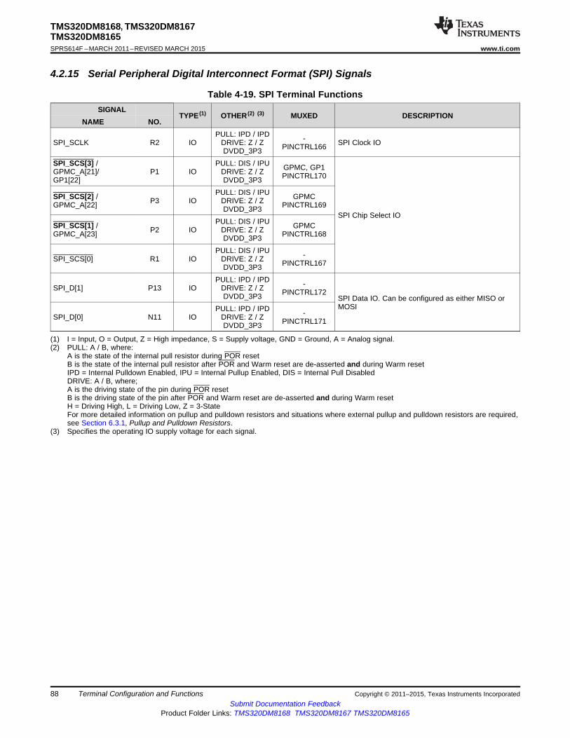
TMS320DM8168, TMS320DM8167TMS320DM8165SPRS614F –MARCH 2011–REVISED MARCH 2015 www.ti.com
4.2.15 Serial Peripheral Digital Interconnect Format (SPI) Signals
Table 4-19. SPI Terminal FunctionsSIGNAL
TYPE (1) OTHER (2) (3) MUXED DESCRIPTIONNAME NO.
PULL: IPD / IPD -SPI_SCLK R2 IO DRIVE: Z / Z SPI Clock IOPINCTRL166DVDD_3P3SPI_SCS[3] / PULL: DIS / IPU GPMC, GP1GPMC_A[21]/ P1 IO DRIVE: Z / Z PINCTRL170GP1[22] DVDD_3P3
PULL: DIS / IPUSPI_SCS[2] / GPMCP3 IO DRIVE: Z / ZGPMC_A[22] PINCTRL169DVDD_3P3SPI Chip Select IO
PULL: DIS / IPUSPI_SCS[1] / GPMCP2 IO DRIVE: Z / ZGPMC_A[23] PINCTRL168DVDD_3P3PULL: DIS / IPU -SPI_SCS[0] R1 IO DRIVE: Z / Z PINCTRL167DVDD_3P3PULL: IPD / IPD -SPI_D[1] P13 IO DRIVE: Z / Z PINCTRL172DVDD_3P3 SPI Data IO. Can be configured as either MISO or
MOSIPULL: IPD / IPD -SPI_D[0] N11 IO DRIVE: Z / Z PINCTRL171DVDD_3P3
(1) I = Input, O = Output, Z = High impedance, S = Supply voltage, GND = Ground, A = Analog signal.(2) PULL: A / B, where:
A is the state of the internal pull resistor during POR resetB is the state of the internal pull resistor after POR and Warm reset are de-asserted and during Warm resetIPD = Internal Pulldown Enabled, IPU = Internal Pullup Enabled, DIS = Internal Pull DisabledDRIVE: A / B, where;A is the driving state of the pin during POR resetB is the driving state of the pin after POR and Warm reset are de-asserted and during Warm resetH = Driving High, L = Driving Low, Z = 3-StateFor more detailed information on pullup and pulldown resistors and situations where external pullup and pulldown resistors are required,see Section 6.3.1, Pullup and Pulldown Resistors.
(3) Specifies the operating IO supply voltage for each signal.
88 Terminal Configuration and Functions Copyright © 2011–2015, Texas Instruments IncorporatedSubmit Documentation Feedback
Product Folder Links: TMS320DM8168 TMS320DM8167 TMS320DM8165

TMS320DM8168, TMS320DM8167TMS320DM8165
www.ti.com SPRS614F –MARCH 2011–REVISED MARCH 2015
4.2.16 Timer Signals
Table 4-20. Timer Terminal FunctionsSIGNAL
TYPE (1) OTHER (2) (3) MUXED DESCRIPTIONNAME NO.
General-Purpose Timers7-1 and Watchdog TimerPULL: IPD / IPDGP0[3]/ GP0J31 I DRIVE: Z / Z Timer external clock inputTCLKIN PINCTRL294DVDD_3P3
Timer7TIM7_OUT/ PULL: IPD / IPD GPMC, GP0GPMC_A[12]/ G1 IO DRIVE: L / L Timer7 capture event input or PWM outputPINCTRL206GP0[31] DVDD_3P3
Timer6TIM6_OUT/ PULL: IPD / IPD GPMC, GP0GPMC_A[24]/ H1 IO DRIVE: L / L Timer6 capture event input or PWM outputPINCTRL205GP0[30] DVDD_3P3
Timer5PULL: IPD / IPDTIM5_OUT/ GP0H34 IO DRIVE: L / L Timer5 capture event input or PWM outputGP0[29] PINCTRL204DVDD_3P3
Timer4PULL: IPD / IPDTIM4_OUT/ GP0H33 IO DRIVE: L / L Timer4 capture event input or PWM outputGP0[28] PINCTRL203DVDD_3P3
Timer3-1There are no external pins on these timers for this device.
Watchdog TimerPULL: IPU / IPU -WD_OUT H36 O DRIVE: H / L Watchdog timer event outputPINCTRL319DVDD_3P3
(1) I = Input, O = Output, Z = High impedance, S = Supply voltage, GND = Ground, A = Analog signal.(2) PULL: A / B, where:
A is the state of the internal pull resistor during POR resetB is the state of the internal pull resistor after POR and Warm reset are de-asserted and during Warm resetIPD = Internal Pulldown Enabled, IPU = Internal Pullup Enabled, DIS = Internal Pull DisabledDRIVE: A / B, where;A is the driving state of the pin during POR resetB is the driving state of the pin after POR and Warm reset are de-asserted and during Warm resetH = Driving High, L = Driving Low, Z = 3-StateFor more detailed information on pullup and pulldown resistors and situations where external pullup and pulldown resistors are required,see Section 6.3.1, Pullup and Pulldown Resistors.
(3) Specifies the operating IO supply voltage for each signal.
Copyright © 2011–2015, Texas Instruments Incorporated Terminal Configuration and Functions 89Submit Documentation Feedback
Product Folder Links: TMS320DM8168 TMS320DM8167 TMS320DM8165

TMS320DM8168, TMS320DM8167TMS320DM8165SPRS614F –MARCH 2011–REVISED MARCH 2015 www.ti.com
4.2.17 Universal Asynchronous Receiver/Transmitter (UART) Signals
Table 4-21. UART0 Terminal FunctionsSIGNAL
TYPE (1) OTHER (2) (3) MUXED DESCRIPTIONNAME NO.
PULL: IPD / IPD UART0 Receive Data Input. Functions as IrDA-UART0_RXD N10 I DRIVE: Z / Z receive input in IrDA modes and CIR receive input inPINCTRL173DVDD_3P3 CIR mode.PULL: IPD / DIS - UART0 Transmit Data Output. Functions as transmitUART0_TXD N8 O DRIVE: L / H PINCTRL174 output in CIR and IrDA modes.DVDD_3P3PULL: IPU / DIS UART0 Request to Send Output. Indicates module isUART0_RTS / GP1N9 O DRIVE: H / H ready to receive data. Functions as SD output in IrDAGP1[27] PINCTRL175DVDD_3P3 mode.PULL: IPU / IPUUART0_CTS / GP1 UART0 Clear to Send Input. Has no function in IrDAN7 I DRIVE: Z / ZGP1[28] PINCTRL176 and CIR modes.DVDD_3P3
UART0_DTR / PULL: IPU / DISGPMC_A[20]/ GPMC, GP1N6 O DRIVE: H / H UART0 Data Terminal Ready OutputGPMC_A[12]/ PINCTRL177DVDD_3P3GP1[16]UART0_DSR / PULL: IPU / IPUGPMC_A[19]/ GPMC, GP1N4 I DRIVE: Z / Z UART0 Data Set Ready InputGPMC_A[24]/ PINCTRL178DVDD_3P3GP1[17]UART0_DCD / PULL: IPU / IPUGPMC_A[18]/ GPMC, GP1N5 I DRIVE: Z / Z UART0 Data Carrier Detect InputGPMC_A[23]/ PINCTRL179DVDD_3P3GP1[18]UART0_RIN/ PULL: IPU / IPUGPMC_A[17]/ GPMC, GP1N3 I DRIVE: Z / Z UART0 Ring Indicator InputGPMC_A[22]/ PINCTRL180DVDD_3P3GP1[19]
(1) I = Input, O = Output, Z = High impedance, S = Supply voltage, GND = Ground, A = Analog signal.(2) PULL: A / B, where:
A is the state of the internal pull resistor during POR resetB is the state of the internal pull resistor after POR and Warm reset are de-asserted and during Warm resetIPD = Internal Pulldown Enabled, IPU = Internal Pullup Enabled, DIS = Internal Pull DisabledDRIVE: A / B, where;A is the driving state of the pin during POR resetB is the driving state of the pin after POR and Warm reset are de-asserted and during Warm resetH = Driving High, L = Driving Low, Z = 3-StateFor more detailed information on pullup and pulldown resistors and situations where external pullup and pulldown resistors are required,see Section 6.3.1, Pullup and Pulldown Resistors.
(3) Specifies the operating IO supply voltage for each signal.
90 Terminal Configuration and Functions Copyright © 2011–2015, Texas Instruments IncorporatedSubmit Documentation Feedback
Product Folder Links: TMS320DM8168 TMS320DM8167 TMS320DM8165

TMS320DM8168, TMS320DM8167TMS320DM8165
www.ti.com SPRS614F –MARCH 2011–REVISED MARCH 2015
Table 4-22. UART1 Terminal FunctionsSIGNAL
TYPE (1) OTHER (2) (3) MUXED DESCRIPTIONNAME NO.
UART1_RXD/ PULL: IPD / IPD UART1 Receive Data Input. Functions as IrDAGPMCGPMC_A[26]/ N1 I DRIVE: Z / Z receive input in IrDA modes and CIR receive input inPINCTRL181GPMC_A[20] DVDD_3P3 CIR mode.UART1_TXD/ PULL: IPD / DIS GPMC UART1 Transmit Data Output. Functions as transmitGPMC_A[25]/ N2 O DRIVE: L / H PINCTRL182 output in CIR and IrDA modes.GPMC_A[19] DVDD_3P3UART1_RTS / PULL: IPU / DIS UART1 Request to Send Output. Indicates module isGPMC_A[14]/ GPMC, GP1M2 O DRIVE: H / H ready to receive data. Functions as SD output in IrDAGPMC_A[18]/ PINCTRL183DVDD_3P3 mode.GP1[25]UART1_CTS / PULL: IPU / IPUGPMC_A[13]/ GPMC, GP1 UART1 Clear to Send Input. Has no function in IrDAL3 IO DRIVE: Z / ZGPMC_A[17]/ PINCTRL184 and CIR modes.DVDD_3P3GP1[26]
(1) I = Input, O = Output, Z = High impedance, S = Supply voltage, GND = Ground, A = Analog signal.(2) PULL: A / B, where:
A is the state of the internal pull resistor during POR resetB is the state of the internal pull resistor after POR and Warm reset are de-asserted and during Warm resetIPD = Internal Pulldown Enabled, IPU = Internal Pullup Enabled, DIS = Internal Pull DisabledDRIVE: A / B, where;A is the driving state of the pin during POR resetB is the driving state of the pin after POR and Warm reset are de-asserted and during Warm resetH = Driving High, L = Driving Low, Z = 3-StateFor more detailed information on pullup and pulldown resistors and situations where external pullup and pulldown resistors are required,see Section 6.3.1, Pullup and Pulldown Resistors.
(3) Specifies the operating IO supply voltage for each signal.
Copyright © 2011–2015, Texas Instruments Incorporated Terminal Configuration and Functions 91Submit Documentation Feedback
Product Folder Links: TMS320DM8168 TMS320DM8167 TMS320DM8165

TMS320DM8168, TMS320DM8167TMS320DM8165SPRS614F –MARCH 2011–REVISED MARCH 2015 www.ti.com
Table 4-23. UART2 Terminal FunctionsSIGNAL
TYPE (1) OTHER (2) (3) MUXED DESCRIPTIONNAME NO.
PULL: IPD / IPD UART2 Receive Data Input. Functions as IrDA-UART2_RXD M1 I DRIVE: Z / Z receive input in IrDA modes and CIR receive input inPINCTRL185DVDD_3P3 CIR mode.PULL: IPD / IPD - UART2 Transmit Data Output. Functions as transmitUART2_TXD L2 O DRIVE: L / H PINCTRL186 output in CIR and IrDA modes.DVDD_3P3
UART2_RTS / PULL: IPU / DIS UART2 Request to Send Output. Indicates module isGPMC_A[15]/ GPMC, GP1L9 O DRIVE: H / H ready to receive data. Functions as SD output in IrDAGPMC_A[26]/ PINCTRL187DVDD_3P3 mode.GP1[23]UART2_CTS / PULL: IPU / IPUGPMC_A[16]/ GPMC, GP1 UART2 Clear to Send Input. Has no function in IrDAK7 IO DRIVE: Z / ZGPMC_A[25]/ PINCTRL188 and CIR modes.DVDD_3P3GP1[24]
(1) I = Input, O = Output, Z = High impedance, S = Supply voltage, GND = Ground, A = Analog signal.(2) PULL: A / B, where:
A is the state of the internal pull resistor during POR resetB is the state of the internal pull resistor after POR and Warm reset are de-asserted and during Warm resetIPD = Internal Pulldown Enabled, IPU = Internal Pullup Enabled, DIS = Internal Pull DisabledDRIVE: A / B, where;A is the driving state of the pin during POR resetB is the driving state of the pin after POR and Warm reset are de-asserted and during Warm resetH = Driving High, L = Driving Low, Z = 3-StateFor more detailed information on pullup and pulldown resistors and situations where external pullup and pulldown resistors are required,see Section 6.3.1, Pullup and Pulldown Resistors.
(3) Specifies the operating IO supply voltage for each signal.
92 Terminal Configuration and Functions Copyright © 2011–2015, Texas Instruments IncorporatedSubmit Documentation Feedback
Product Folder Links: TMS320DM8168 TMS320DM8167 TMS320DM8165

TMS320DM8168, TMS320DM8167TMS320DM8165
www.ti.com SPRS614F –MARCH 2011–REVISED MARCH 2015
4.2.18 Universal Serial Bus (USB) Signals
Table 4-24. USB Terminal FunctionsSIGNAL
TYPE (1) OTHER (2) (3) MUXED DESCRIPTIONNAME NO.
USB0USB0_DP P37 A IO - - USB0 bidirectional Data Differential signal pair
[positive/negative].
USB0_DN P36 A IO - - When the USB0 PHY is powered down, these pinsshould be left unconnected.USB0 current reference output. When the USB0peripheral is used, this pin must be connected via a44.2-Ω ±1% resistor to VSS.USB0_R1 N37 A O - -When the USB0 PHY is powered down, this pinshould be left unconnected.When this pin is used as USB0_DRVVBUS and theUSB0 Controller is operating as a Host, this signal is
PULL: IPD / IPD used by the USB0 Controller to enable the external-USB0_DRVVBUS P35 O DRIVE: L / L VBUS charge pump.PINCTRL322DVDD_3P3When the USB0 PHY is powered down, this pinshould be left unconnected.USB0 VBUS input (5 V).The voltage level on this pin is sampled to determinesession status.VDD_USB0_VBUS N36 I - -When the USB0 PHY is powered down, this pinshould be left unconnected.
USB1USB1_DP R37 A IO - - USB1 bidirectional Data Differential signal pair
[positive/negative].
USB1_DN R36 A IO - - When the USB1 PHY is powered down, these pinsshould be left unconnected.USB1 current reference output. When the USB1peripheral is used, this pin must be connected via a44.2-Ω ±1% resistor to VSS.USB1_R1 T37 A O - -When the USB1 PHY is powered down, this pinshould be left unconnected.When this pin is used as USB1_DRVVBUS and theUSB1 Controller is operating as a Host, this signal is
PULL: IPD / IPD used by the USB1 Controller to enable the external-USB1_DRVVBUS R35 O DRIVE: L / L VBUS charge pump.PINCTRL323DVDD_3P3When the USB1 PHY is powered down, this pinshould be left unconnected.USB1 VBUS input (5 V).The voltage level on this pin is sampled to determinesession status.VDD_USB1_VBUS T36 I - -When the USB1 PHY is powered down, this pinshould be left unconnected.
(1) I = Input, O = Output, Z = High impedance, S = Supply voltage, GND = Ground, A = Analog signal.(2) PULL: A / B, where:
A is the state of the internal pull resistor during POR resetB is the state of the internal pull resistor after POR and Warm reset are de-asserted and during Warm resetIPD = Internal Pulldown Enabled, IPU = Internal Pullup Enabled, DIS = Internal Pull DisabledDRIVE: A / B, where;A is the driving state of the pin during POR resetB is the driving state of the pin after POR and Warm reset are de-asserted and during Warm resetH = Driving High, L = Driving Low, Z = 3-StateFor more detailed information on pullup and pulldown resistors and situations where external pullup and pulldown resistors are required,see Section 6.3.1, Pullup and Pulldown Resistors.
(3) Specifies the operating IO supply voltage for each signal.
Copyright © 2011–2015, Texas Instruments Incorporated Terminal Configuration and Functions 93Submit Documentation Feedback
Product Folder Links: TMS320DM8168 TMS320DM8167 TMS320DM8165

TMS320DM8168, TMS320DM8167TMS320DM8165SPRS614F –MARCH 2011–REVISED MARCH 2015 www.ti.com
4.2.19 Video Input Signals
Table 4-25. Video Input 0 Terminal FunctionsSIGNAL
TYPE (1) OTHER (2) (3) MUXED DESCRIPTIONNAME NO.
PULL: IPD / IPD - Video Input 0 Port A Clock input. Input clock for 8-bit,VIN[0]A_CLK AR14 I DRIVE: Z / Z PINCTRL83 16-bit, or 24-bit Port A video capture.DVDD_3P3PULL: IPD / IPD Video Input 0 Port B Clock input. Input clock for 8-bit-VIN[0]B_CLK AR19 I DRIVE: Z / Z Port B video capture. This signal is not used in 16-bitPINCTRL84DVDD_3P3 and 24-bit capture modes.PULL: IPD / IPDVIN[0]A_D[23]/ VIN[0]BAT2 I DRIVE: Z / ZVIN[0]B_HSYNC PINCTRL15DVDD_3P3PULL: IPD / IPDVIN[0]A_D[22]/ VIN[0]BAR2 I DRIVE: Z / ZVIN[0]B_VSYNC PINCTRL14DVDD_3P3PULL: IPD / IPDVIN[0]A_D[21]/ VIN[0]BAU4 I DRIVE: Z / ZVIN[0]B_FLD PINCTRL13DVDD_3P3PULL: IPD / IPDVIN[0]A_D[20]/ VIN[0]BAN3 I DRIVE: Z / ZVIN[0]B_DE PINCTRL12 Video Input 0 Port A Data inputs. For 16-bit capture,DVDD_3P3
D[7:0] are Cb/Cr and [15:8] are Y Port A inputs. ForVIN[0]A_D[19]/ PULL: IPD / IPD VIN[1]A, 8-bit capture, D[7:0] are Port A YCbCr data inputsVIN[1]A_DE[0]/ AK4 I DRIVE: Z / Z VOUT[1] and D[15:8] are Port B YCbCr data inputs. For RGBVOUT[1]_C[9] DVDD_3P3 PINCTRL25 capture, D[23:16] are R, D[15:8] are G, and D[7:0] are
B data inputs.VIN[0]A_D[18]/ PULL: IPD / IPD VIN[1]A,VIN[1]A_FLD/ AK5 I DRIVE: Z / Z VOUT[1]VOUT[1]_C[8] DVDD_3P3 PINCTRL24VIN[0]A_D[17]/VIN[1]A_VSYNC/ PULL: IPD / IPD VIN[1]A,VOUT[1]_VSYNC AL5 I DRIVE: Z / Z VOUT[1](silicon revision 1.x) DVDD_3P3 PINCTRL23DAC_VOUT[1]_VSYNC(silicon revision 2.x)VIN[0]A_D[16]/ PULL: IPD / IPD VIN[1]A,VIN[1]A_HSYNC/ AT5 I DRIVE: Z / Z VOUT[1]VOUT[1]_FLD DVDD_3P3 PINCTRL22
(1) I = Input, O = Output, Z = High impedance, S = Supply voltage, GND = Ground, A = Analog signal.(2) PULL: A / B, where:
A is the state of the internal pull resistor during POR resetB is the state of the internal pull resistor after POR and Warm reset are de-asserted and during Warm resetIPD = Internal Pulldown Enabled, IPU = Internal Pullup Enabled, DIS = Internal Pull DisabledDRIVE: A / B, where;A is the driving state of the pin during POR resetB is the driving state of the pin after POR and Warm reset are de-asserted and during Warm resetH = Driving High, L = Driving Low, Z = 3-StateFor more detailed information on pullup and pulldown resistors and situations where external pullup and pulldown resistors are required,see Section 6.3.1, Pullup and Pulldown Resistors.
(3) Specifies the operating IO supply voltage for each signal.
94 Terminal Configuration and Functions Copyright © 2011–2015, Texas Instruments IncorporatedSubmit Documentation Feedback
Product Folder Links: TMS320DM8168 TMS320DM8167 TMS320DM8165
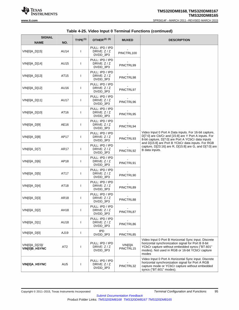
TMS320DM8168, TMS320DM8167TMS320DM8165
www.ti.com SPRS614F –MARCH 2011–REVISED MARCH 2015
Table 4-25. Video Input 0 Terminal Functions (continued)SIGNAL
TYPE (1) OTHER (2) (3) MUXED DESCRIPTIONNAME NO.
PULL: IPD / IPD -VIN[0]A_D[15] AU14 I DRIVE: Z / Z PINCTRL100DVDD_3P3PULL: IPD / IPD -VIN[0]A_D[14] AU15 I DRIVE: Z / Z PINCTRL99DVDD_3P3PULL: IPD / IPD -VIN[0]A_D[13] AT15 I DRIVE: Z / Z PINCTRL98DVDD_3P3PULL: IPD / IPD -VIN[0]A_D[12] AU16 I DRIVE: Z / Z PINCTRL97DVDD_3P3PULL: IPD / IPD -VIN[0]A_D[11] AU17 I DRIVE: Z / Z PINCTRL96DVDD_3P3PULL: IPD / IPD -VIN[0]A_D[10] AT16 I DRIVE: Z / Z PINCTRL95DVDD_3P3PULL: IPD / IPD -VIN[0]A_D[9] AE16 I DRIVE: Z / Z PINCTRL94DVDD_3P3
Video Input 0 Port A Data inputs. For 16-bit capture,PULL: IPD / IPD - D[7:0] are Cb/Cr and [15:8] are Y Port A inputs. ForVIN[0]A_D[8] AP17 I DRIVE: Z / Z PINCTRL93 8-bit capture, D[7:0] are Port A YCbCr data inputsDVDD_3P3and D[15:8] are Port B YCbCr data inputs. For RGB
PULL: IPD / IPD capture, D[23:16] are R, D[15:8] are G, and D[7:0] are-VIN[0]A_D[7] AR17 I DRIVE: Z / Z B data inputs.PINCTRL92DVDD_3P3PULL: IPD / IPD -VIN[0]A_D[6] AP18 I DRIVE: Z / Z PINCTRL91DVDD_3P3PULL: IPD / IPD -VIN[0]A_D[5] AT17 I DRIVE: Z / Z PINCTRL90DVDD_3P3PULL: IPD / IPD -VIN[0]A_D[4] AT18 I DRIVE: Z / Z PINCTRL89DVDD_3P3PULL: IPD / IPD -VIN[0]A_D[3] AR18 I DRIVE: Z / Z PINCTRL88DVDD_3P3PULL: IPD / IPD -VIN[0]A_D[2] AH18 I DRIVE: Z / Z PINCTRL87DVDD_3P3PULL: IPD / IPD -VIN[0]A_D[1] AU18 I DRIVE: Z / Z PINCTRL86DVDD_3P3
IPD -VIN[0]A_D[0] AJ19 I DVDD_3P3 PINCTRL85Video Input 0 Port B Horizontal Sync input. Discrete
PULL: IPD / IPD horizontal synchronization signal for Port B 8-bitVIN[0]A_D[23]/ VIN[0]AAT2 I DRIVE: Z / Z YCbCr capture without embedded syncs ("BT.601"VIN[0]B_HSYNC PINCTRL15DVDD_3P3 modes). Not used in RGB or 16-bit YCbCr capturemodesVideo Input 0 Port A Horizontal Sync input. DiscretePULL: IPD / IPD - horizontal synchronization signal for Port A RGBVIN[0]A_HSYNC AU5 I DRIVE: Z / Z PINCTRL32 capture mode or YCbCr capture without embeddedDVDD_3P3 syncs ("BT.601" modes).
Copyright © 2011–2015, Texas Instruments Incorporated Terminal Configuration and Functions 95Submit Documentation Feedback
Product Folder Links: TMS320DM8168 TMS320DM8167 TMS320DM8165

TMS320DM8168, TMS320DM8167TMS320DM8165SPRS614F –MARCH 2011–REVISED MARCH 2015 www.ti.com
Table 4-25. Video Input 0 Terminal Functions (continued)SIGNAL
TYPE (1) OTHER (2) (3) MUXED DESCRIPTIONNAME NO.
Video Input 0 Port B Vertical Sync input. DiscretePULL: IPD / IPDVIN[0]A_D[22]/ VIN[0]A vertical synchronization signal for Port B 8-bit YCbCrAR2 I DRIVE: Z / ZVIN[0]B_VSYNC PINCTRL14 capture without embedded syncs ("BT.601" modes).DVDD_3P3 Not used in RGB or 16-bit YCbCr capture modes.Video Input 0 Port A Vertical Sync input. DiscretePULL: IPD / IPD - vertical synchronization signal for Port A RGB captureVIN[0]A_VSYNC AM4 I DRIVE: Z / Z PINCTRL33 mode or YCbCr capture without embedded syncsDVDD_3P3 ("BT.601" modes).Video Input 0 Port B Field ID input. Discrete fieldPULL: IPD / IPDVIN[0]A_D[21]/ VIN[0]A identification signal for Port B 8-bit YCbCr captureAU4 I DRIVE: Z / ZVIN[0]B_FLD PINCTRL13 without embedded syncs ("BT.601" modes). Not usedDVDD_3P3 in RGB or 16-bit YCbCr capture modesVideo Input 0 Port A Field ID input. Discrete fieldPULL: IPD / IPD - identification signal for Port A RGB capture mode orVIN[0]A_FLD AL4 I DRIVE: Z / Z PINCTRL34 YCbCr capture without embedded syncs ("BT.601"DVDD_3P3 modes).
PULL: IPD / IPD Video Input 0 Port B Data Enable input. Discrete dataVIN[0]A_D[20]/ VIN[0]AAN3 I DRIVE: Z / Z valid signal for Port B RGB capture mode or YCbCrVIN[0]B_DE PINCTRL12DVDD_3P3 capture without embedded syncs ("BT.601" modes).PULL: IPD / IPD Video Input 0 Port A Data Enable input. Discrete data-VIN[0]A_DE AT3 I DRIVE: Z / Z valid signal for Port A RGB capture mode or YCbCrPINCTRL35DVDD_3P3 capture without embedded syncs ("BT.601" modes).
96 Terminal Configuration and Functions Copyright © 2011–2015, Texas Instruments IncorporatedSubmit Documentation Feedback
Product Folder Links: TMS320DM8168 TMS320DM8167 TMS320DM8165
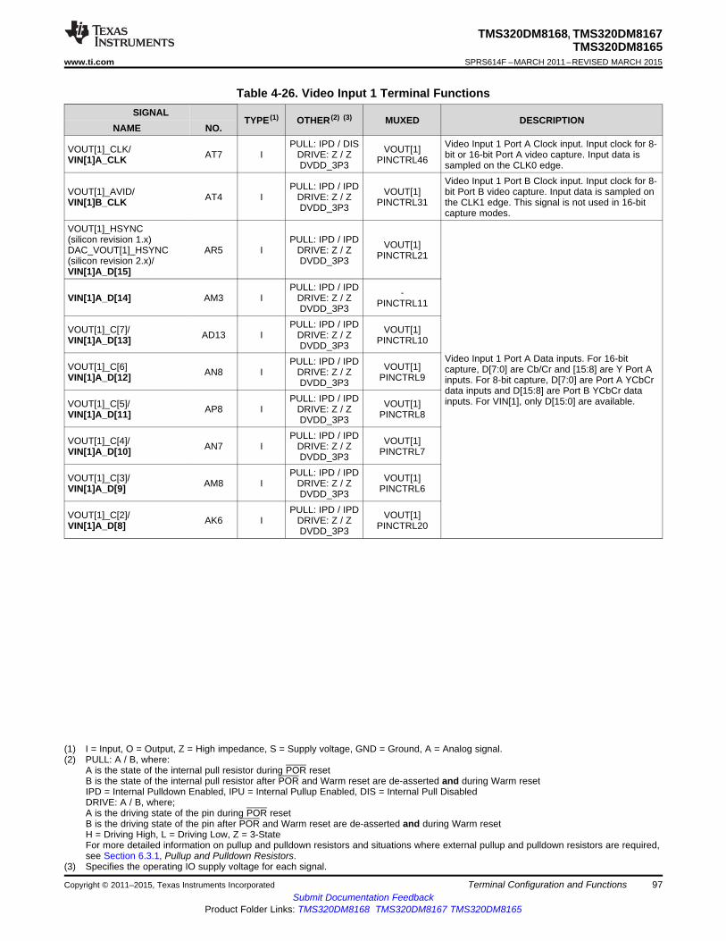
TMS320DM8168, TMS320DM8167TMS320DM8165
www.ti.com SPRS614F –MARCH 2011–REVISED MARCH 2015
Table 4-26. Video Input 1 Terminal FunctionsSIGNAL
TYPE (1) OTHER (2) (3) MUXED DESCRIPTIONNAME NO.
PULL: IPD / DIS Video Input 1 Port A Clock input. Input clock for 8-VOUT[1]_CLK/ VOUT[1]AT7 I DRIVE: Z / Z bit or 16-bit Port A video capture. Input data isVIN[1]A_CLK PINCTRL46DVDD_3P3 sampled on the CLK0 edge.Video Input 1 Port B Clock input. Input clock for 8-PULL: IPD / IPDVOUT[1]_AVID/ VOUT[1] bit Port B video capture. Input data is sampled onAT4 I DRIVE: Z / ZVIN[1]B_CLK PINCTRL31 the CLK1 edge. This signal is not used in 16-bitDVDD_3P3 capture modes.
VOUT[1]_HSYNC(silicon revision 1.x) PULL: IPD / IPD VOUT[1]DAC_VOUT[1]_HSYNC AR5 I DRIVE: Z / Z PINCTRL21(silicon revision 2.x)/ DVDD_3P3VIN[1]A_D[15]
PULL: IPD / IPD -VIN[1]A_D[14] AM3 I DRIVE: Z / Z PINCTRL11DVDD_3P3PULL: IPD / IPDVOUT[1]_C[7]/ VOUT[1]AD13 I DRIVE: Z / ZVIN[1]A_D[13] PINCTRL10DVDD_3P3
Video Input 1 Port A Data inputs. For 16-bitPULL: IPD / IPDVOUT[1]_C[6] VOUT[1] capture, D[7:0] are Cb/Cr and [15:8] are Y Port AAN8 I DRIVE: Z / ZVIN[1]A_D[12] PINCTRL9 inputs. For 8-bit capture, D[7:0] are Port A YCbCrDVDD_3P3data inputs and D[15:8] are Port B YCbCr data
PULL: IPD / IPD inputs. For VIN[1], only D[15:0] are available.VOUT[1]_C[5]/ VOUT[1]AP8 I DRIVE: Z / ZVIN[1]A_D[11] PINCTRL8DVDD_3P3PULL: IPD / IPDVOUT[1]_C[4]/ VOUT[1]AN7 I DRIVE: Z / ZVIN[1]A_D[10] PINCTRL7DVDD_3P3PULL: IPD / IPDVOUT[1]_C[3]/ VOUT[1]AM8 I DRIVE: Z / ZVIN[1]A_D[9] PINCTRL6DVDD_3P3PULL: IPD / IPDVOUT[1]_C[2]/ VOUT[1]AK6 I DRIVE: Z / ZVIN[1]A_D[8] PINCTRL20DVDD_3P3
(1) I = Input, O = Output, Z = High impedance, S = Supply voltage, GND = Ground, A = Analog signal.(2) PULL: A / B, where:
A is the state of the internal pull resistor during POR resetB is the state of the internal pull resistor after POR and Warm reset are de-asserted and during Warm resetIPD = Internal Pulldown Enabled, IPU = Internal Pullup Enabled, DIS = Internal Pull DisabledDRIVE: A / B, where;A is the driving state of the pin during POR resetB is the driving state of the pin after POR and Warm reset are de-asserted and during Warm resetH = Driving High, L = Driving Low, Z = 3-StateFor more detailed information on pullup and pulldown resistors and situations where external pullup and pulldown resistors are required,see Section 6.3.1, Pullup and Pulldown Resistors.
(3) Specifies the operating IO supply voltage for each signal.
Copyright © 2011–2015, Texas Instruments Incorporated Terminal Configuration and Functions 97Submit Documentation Feedback
Product Folder Links: TMS320DM8168 TMS320DM8167 TMS320DM8165

TMS320DM8168, TMS320DM8167TMS320DM8165SPRS614F –MARCH 2011–REVISED MARCH 2015 www.ti.com
Table 4-26. Video Input 1 Terminal Functions (continued)SIGNAL
TYPE (1) OTHER (2) (3) MUXED DESCRIPTIONNAME NO.
PULL: IPD / IPDVOUT[1]_Y_YC[9]/ VOUT[1]AP6 I DRIVE: Z / ZVIN[1]A_D[7] PINCTRL19DVDD_3P3PULL: IPD / IPDVOUT[1]_Y_YC[8]/ VOUT[1]AT6 I DRIVE: Z / ZVIN[1]A_D[6] PINCTRL18DVDD_3P3PULL: IPD / IPDVOUT[1]_Y_YC[7]/ VOUT[1]AR6 I DRIVE: Z / ZVIN[1]A_D[5] PINCTRL17DVDD_3P3PULL: IPD / IPDVOUT[1]_Y_YC[6]/ VOUT[1] Video Input 1 Port A Data inputs. For 16-bitAC13 I DRIVE: Z / ZVIN[1]A_D[4] PINCTRL16 capture, D[7:0] are Cb/Cr and [15:8] are Y Port ADVDD_3P3
inputs. For 8-bit capture, D[7:0] are Port A YCbCrPULL: IPD / DIS data inputs and D[15:8] are Port B YCbCr dataVOUT[1]_Y_YC[5]/ VOUT[1]AJ7 I DRIVE: Z / Z inputs. For VIN[1], only D[15:0] are available.VIN[1]A_D[3] PINCTRL50DVDD_3P3PULL: IPD / DISVOUT[1]_Y_YC[4]/ VOUT[1]AU6 I DRIVE: Z / ZVIN[1]A_D[2] PINCTRL49DVDD_3P3PULL: IPD / DISVOUT[1]_Y_YC[3]/ VOUT[1]AP7 I DRIVE: Z / ZVIN[1]A_D[1] PINCTRL48DVDD_3P3PULL: IPD / DISVOUT[1]_Y_YC[2]/ VOUT[1]AU7 I DRIVE: Z / ZVIN[1]A_D[0] PINCTRL47DVDD_3P3
Video Input 1 Port B Horizontal Sync or Data ValidVOUT[0]_B_CB_C[0]/ PULL: IPD / IPD VOUT[0], signal input. Discrete horizontal synchronizationVOUT[1]_C[9]/ AR9 I DRIVE: Z / Z VOUT[1] signal for Port B 8-bit YCbCr capture withoutVIN[1]B_HSYNC_DE DVDD_3P3 PINCTRL27 embedded syncs ("BT.601" modes). Not used in
16-bit YCbCr capture mode.Video Input 1 Port A Horizontal Sync input.VIN[0]A_D[16]/ PULL: IPD / IPD VIN[0]A, Discrete horizontal synchronization signal for PortVIN[1]A_HSYNC/ AT5 I DRIVE: Z / Z VOUT[1] A YCbCr capture modes without embedded syncsVOUT[1]_FLD DVDD_3P3 PINCTRL22 ("BT.601" modes).
VOUT[0]_G_Y_YC[0]/VOUT[1]_VSYNC Video Input 1 Port B Vertical Sync input. DiscretePULL: IPD / IPD VOUT[0],(silicon revision 1.x) vertical synchronization signal for Port B 8-bitAP9 I DRIVE: Z / Z VOUT[1]DAC_VOUT[1]_VSYNC YCbCr capture without embedded syncs ("BT.601"DVDD_3P3 PINCTRL29(silicon revision 2.x)/ modes). Not used in 16-bit YCbCr capture mode.VIN[1]B_VSYNCVIN[0]A_D[17]/VIN[1]A_VSYNC/ Video Input 1 Port A Vertical Sync input. DiscretePULL: IPD / IPD VIN[0]A,VOUT[1]_VSYNC vertical synchronization signal for Port A YCbCrAL5 I DRIVE: Z / Z VOUT[1](silicon revision 1.x) capture modes without embedded syncs ("BT.601"DVDD_3P3 PINCTRL23DAC_VOUT[1]_VSYNC modes).(silicon revision 2.x)VIN[0]A_D[19]/ PULL: IPD / IPD VIN[0]A, Video Input 1 Port A Data Enable input. DiscreteVIN[1]A_DE/ AK4 I DRIVE: Z / Z VOUT[1] data valid signal for Port A YCbCr capture modesVOUT[1]_C[9] DVDD_3P3 PINCTRL25 without embedded syncs ("BT.601" modes).
Video Input 1Port A Field ID input. Discrete fieldVIN[0]A_D[18]/ PULL: IPD / IPD VIN[0]A, identification signal for Port A YCbCr captureVIN[1]A_FLD/ AK5 I DRIVE: Z / Z VOUT[1] modes without embedded syncs ("BT.601"VOUT[1]_C[8] DVDD_3P3 PINCTRL24 modes).Video Input 1 Port B Field ID input. Discrete fieldVOUT[0]_G_Y_YC[1]/ PULL: IPD / IPD VOUT[0], identification signal for Port B 8-bit YCbCr captureVOUT[1]_FLD/ AU8 I DRIVE: Z / Z VOUT[1] without embedded syncs ("BT.601" modes). NotVIN[1]B_FLD DVDD_3P3 PINCTRL30 used in 16-bit YCbCr capture mode.
98 Terminal Configuration and Functions Copyright © 2011–2015, Texas Instruments IncorporatedSubmit Documentation Feedback
Product Folder Links: TMS320DM8168 TMS320DM8167 TMS320DM8165

TMS320DM8168, TMS320DM8167TMS320DM8165
www.ti.com SPRS614F –MARCH 2011–REVISED MARCH 2015
4.2.20 Digital Video Output Signals
NOTEVideo output 0 pins AR8 and AL9 and video output 1 pins AT9, AR5, AP9, and AL5 have adifferent naming convention and functionality for silicon revision 1.x devices and siliconrevision 2.x devices. These pins are listed separately in Table 4-28 and Table 4-30.
Table 4-27. Video Output 0 Terminal FunctionsSIGNAL
TYPE (1) OTHER (2) (3) MUXED DESCRIPTIONNAME NO.
PULL: IPD / DIS -VOUT[0]_CLK AT14 O DRIVE: L / H Video Output 0 Clock output.PINCTRL101DVDD_3P3PULL: IPD / DIS -VOUT[0]_G_Y_YC[9] AR13 O DRIVE: L / L PINCTRL109DVDD_3P3PULL: IPD / DIS -VOUT[0]_G_Y_YC[8] AU13 O DRIVE: L / L PINCTRL108DVDD_3P3PULL: IPD / DIS -VOUT[0]_G_Y_YC[7] AT13 O DRIVE: L / L PINCTRL107DVDD_3P3
Video Output 0 Data. These signals represent thePULL: IPD / DIS - 8 MSBs of G/Y/YC video data. For RGB modeVOUT[0]_G_Y_YC[6] AE14 O DRIVE: L / L PINCTRL106 they are green data bits, for YUV444 mode theyDVDD_3P3are Y data bits, for Y/C mode they are Y (Luma)
PULL: IPD / DIS data bits and for BT.656 mode they are-VOUT[0]_G_Y_YC[5] AM14 O DRIVE: L / L multiplexed Y/Cb/Cr (Luma and Chroma) dataPINCTRL105DVDD_3P3 bits.PULL: IPD / DIS -VOUT[0]_G_Y_YC[4] AL14 O DRIVE: L / L PINCTRL104DVDD_3P3PULL: IPD / DIS -VOUT[0]_G_Y_YC[3] AP14 O DRIVE: L / L PINCTRL103DVDD_3P3PULL: IPD / DIS -VOUT[0]_G_Y_YC[2] AE15 O DRIVE: L / L PINCTRL102DVDD_3P3
VOUT[0]_G_Y_YC[1]/ PULL: IPD / IPD VOUT,[1] Video Output 0 Data. These signals represent theVOUT[1]_FLD/ AU8 O DRIVE: Z / Z VIN[1]B 2 LSBs of G/Y/YC video data for 10-bit, 20-bit andVIN[1]B_FLD DVDD_3P3 PINCTRL30 30-bit video modes (VOUT0 only). For RGB mode
they are green data bits, for YUV444 mode theyVOUT[0]_G_Y_YC[0]/are Y data bits, for Y/C mode they are Y (Luma)VOUT[1]_VSYNC PULL: IPD / IPD VOUT[1], data bits and for BT.656 mode they are(silicon revision 1.x) AP9 O DRIVE: Z / Z VIN[1]B multiplexed Y/Cb/Cr (Luma and Chroma) dataDAC_VOUT[1]_VSYNC DVDD_3P3 PINCTRL29 bits. These signals are not used in 8/16/24-bit(silicon revision 2.x)/modesVIN[1]B_VSYNC
(1) I = Input, O = Output, Z = High impedance, S = Supply voltage, GND = Ground, A = Analog signal.(2) PULL: A / B, where:
A is the state of the internal pull resistor during POR resetB is the state of the internal pull resistor after POR and Warm reset are de-asserted and during Warm resetIPD = Internal Pulldown Enabled, IPU = Internal Pullup Enabled, DIS = Internal Pull DisabledDRIVE: A / B, where;A is the driving state of the pin during POR resetB is the driving state of the pin after POR and Warm reset are de-asserted and during Warm resetH = Driving High, L = Driving Low, Z = 3-StateFor more detailed information on pullup and pulldown resistors and situations where external pullup and pulldown resistors are required,see Section 6.3.1, Pullup and Pulldown Resistors.
(3) Specifies the operating IO supply voltage for each signal.
Copyright © 2011–2015, Texas Instruments Incorporated Terminal Configuration and Functions 99Submit Documentation Feedback
Product Folder Links: TMS320DM8168 TMS320DM8167 TMS320DM8165

TMS320DM8168, TMS320DM8167TMS320DM8165SPRS614F –MARCH 2011–REVISED MARCH 2015 www.ti.com
Table 4-27. Video Output 0 Terminal Functions (continued)SIGNAL
TYPE (1) OTHER (2) (3) MUXED DESCRIPTIONNAME NO.
PULL: IPD / DIS -VOUT[0]_B_CB_C[9] AT12 O DRIVE: L / L PINCTRL117DVDD_3P3PULL: IPD / DIS -VOUT[0]_B_CB_C[8] AH13 O DRIVE: L / L PINCTRL116DVDD_3P3PULL: IPD / DIS -VOUT[0]_B_CB_C[7] AM13 O DRIVE: L / L PINCTRL115DVDD_3P3PULL: IPD / DIS Video Output 0 Data. These signals represent the-VOUT[0]_B_CB_C[6] AJ13 O DRIVE: L / L 8 MSBs of B/CB/C video data. For RGB modePINCTRL114DVDD_3P3 they are blue data bits, for YUV444 mode they are
Cb (Chroma) data bits, for Y/C mode they arePULL: IPD / DIS - multiplexed Cb/Cr (Chroma) data bits and forVOUT[0]_B_CB_C[5] AK13 O DRIVE: L / L PINCTRL113 BT.656 mode they are unusedDVDD_3P3PULL: IPD / DIS -VOUT[0]_B_CB_C[4] AN13 O DRIVE: L / L PINCTRL112DVDD_3P3PULL: IPD / DIS -VOUT[0]_B_CB_C[3] AL13 O DRIVE: L / L PINCTRL111DVDD_3P3PULL: IPD / DIS -VOUT[0]_B_CB_C[2] AP13 O DRIVE: L / L PINCTRL110DVDD_3P3
VOUT[0]_B_CB_C[1]/VOUT[1]_HSYNC PULL: IPD / IPD(silicon revision 1.x) VOUT[1]AT9 O DRIVE: Z / ZDAC_VOUT[1]_HSYNC PINCTRL28DVDD_3P3(silicon revision 2.x)/ Video Output 0 Data. These signals represent theVOUT[1]_AVID 2 LSBs of B/CB/C video data for 20-bit and 30-bit
video modes (VOUT[0] only). For RGB mode theyVOUT[0]_R_CR[9]/ PULL: IPD / DIS VOUT[0],are blue data bits, for YUV444 mode they are CbVOUT[0]_B_CB_C[1]/ AU9 O DRIVE: L / L VOUT[1](Chroma) data bits, for Y/C mode they areVOUT[1]_Y_YC[9] DVDD_3P3 PINCTRL125multiplexed Cb/Cr (Chroma) data bits and for
VOUT[0]_B_CB_C[0]/ PULL: IPD / IPD VOUT[1], BT.656 mode they are unused. These signals areVOUT[1]_C[9]/ AR9 O DRIVE: Z / Z VIN[1]B not used in 16/24-bit modes.VIN[1]B_HSYNC_DE DVDD_3P3 PINCTRL27VOUT[0]_R_CR[8]/ PULL: IPD / DIS VOUT[0],VOUT[0]_B_CB_C[0]/ AK10 O DRIVE: L / L VOUT[1]VOUT[1]_Y_YC[8] DVDD_3P3 PINCTRL124
100 Terminal Configuration and Functions Copyright © 2011–2015, Texas Instruments IncorporatedSubmit Documentation Feedback
Product Folder Links: TMS320DM8168 TMS320DM8167 TMS320DM8165

TMS320DM8168, TMS320DM8167TMS320DM8165
www.ti.com SPRS614F –MARCH 2011–REVISED MARCH 2015
Table 4-27. Video Output 0 Terminal Functions (continued)SIGNAL
TYPE (1) OTHER (2) (3) MUXED DESCRIPTIONNAME NO.
VOUT[0]_R_CR[9]/ PULL: IPD / DIS VOUT[0],VOUT[0]_B_CB_C[1]/ AU9 O DRIVE: L / L VOUT[1]VOUT[1]_Y_YC[9] DVDD_3P3 PINCTRL125VOUT[0]_R_CR[8]/ PULL: IPD / DIS VOUT[0],VOUT[0]_B_CB_C[0]/ AK10 O DRIVE: L / L VOUT[1]VOUT[1]_Y_YC[8] DVDD_3P3 PINCTRL124VOUT[0]_R_CR[7]/ PULL: IPD / DIS VOUT[0],VOUT[0]_G_Y_YC[1]/ AL10 O DRIVE: L / L VOUT[1]VOUT[1]_Y_YC[7] DVDD_3P3 PINCTRL123VOUT[0]_R_CR[6]/ PULL: IPD / DIS VOUT[0],
Video Output 0 Data. These signals represent theVOUT[0]_G_Y_YC[0]/ AU10 O DRIVE: L / L VOUT[1]8 MSBs of R/CR video data. For RGB mode theyVOUT[1]_Y_YC[6] DVDD_3P3 PINCTRL122are red data bits, for YUV444 mode they are Cr
VOUT[0]_R_CR[5]/ PULL: IPD / DIS VOUT[0], (Chroma) data bits, for Y/C mode and BT.656VOUT[0]_AVID/ AT10 O DRIVE: L / L VOUT[1] modes they are unused.VOUT[1]_Y_YC[5] DVDD_3P3 PINCTRL121VOUT[0]_R_CR[4]/ PULL: IPD / DIS VOUT[0],VOUT[0]_FLD/ AG13 O DRIVE: L / L VOUT[1]VOUT[1]_Y_YC[4] DVDD_3P3 PINCTRL120VOUT[0]_R_CR[3]/ PULL: IPD / DIS VOUT[0],VOUT[0]_VSYNC/ AR11 O DRIVE: L / L VOUT[1]VOUT[1]_Y_YC[3] DVDD_3P3 PINCTRL119VOUT[0]_R_CR[2]/ PULL: IPD / DIS VOUT[0],VOUT[0]_HSYNC/ AT11 O DRIVE: L / L VOUT[1]VOUT[1]_Y_YC[2] DVDD_3P3 PINCTRL118
PULL: IPD / IPD Video Output 0 Data. These signals represent the-VOUT[0]_R_CR[1] AT8 O DRIVE: Z / Z 2 LSBs of R/CR video data for 30-bit video modesPINCTRL40DVDD_3P3 (VOUT[0] only). For RGB mode they are red databits, for YUV444 mode they are Cr (Chroma) data
VOUT[0]_R_CR[0]/ PULL: IPD / IPD bits, for Y/C mode and BT.656 modes they areVOUT[1]VOUT[1]_C[8]/ AJ11 O DRIVE: Z / Z unused. These signals are not used in 24-bitPINCTRL26VOUT[1]_CLK DVDD_3P3 mode.PULL: IPD / IPD -VOUT[0]_VSYNC AN9 O DRIVE: Z / Z PINCTRL37 Video Output 0 Vertical Sync output. This is theDVDD_3P3
discrete vertical synchronization output. ThisVOUT[0]_R_CR[3]/ PULL: IPD / DIS VOUT[0], signal is not used for embedded sync modes.VOUT[0]_VSYNC/ AR11 O DRIVE: L / L VOUT[1]VOUT[1]_Y_YC[3] DVDD_3P3 PINCTRL119
PULL: IPD / IPD -VOUT[0]_HSYNC AM9 O DRIVE: Z / Z PINCTRL36 Video Output 0 Horizontal Sync output. This is theDVDD_3P3discrete horizontal synchronization output. This
VOUT[0]_R_CR[2]/ PULL: IPD / DIS VOUT[0], signal is not used for embedded sync modes.VOUT[0]_HSYNC/ AT11 O DRIVE: L / L VOUT[1]VOUT[1]_Y_YC[2] DVDD_3P3 PINCTRL118VOUT[0]_R_CR[4]/ PULL: IPD / DIS VOUT[0], Video Output 0 Field ID output. This is the discreteVOUT[0]_FLD/ AG13 O DRIVE: L / L VOUT[1] field identification output. This signal is not usedVOUT[1]_Y_YC[4] DVDD_3P3 PINCTRL120 for embedded sync modes.VOUT[0]_R_CR[5]/ PULL: IPD / DIS VOUT[0], Video Output 0 Active Video output. This is theVOUT[0]_AVID/ AT10 O DRIVE: L / L VOUT[1] discrete active video indicator output. This signalVOUT[1]_Y_YC[5] DVDD_3P3 PINCTRL121 is not used for embedded sync modes.
Copyright © 2011–2015, Texas Instruments Incorporated Terminal Configuration and Functions 101Submit Documentation Feedback
Product Folder Links: TMS320DM8168 TMS320DM8167 TMS320DM8165
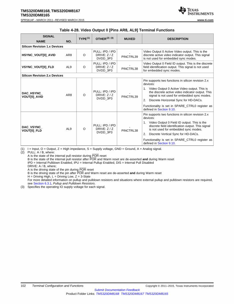
TMS320DM8168, TMS320DM8167TMS320DM8165SPRS614F –MARCH 2011–REVISED MARCH 2015 www.ti.com
Table 4-28. Video Output 0 [Pins AR8, AL9] Terminal FunctionsSIGNAL
TYPE (1) OTHER (2) (3) MUXED DESCRIPTIONNAME NO.
Silicon Revision 1.x DevicesPULL: IPD / IPD Video Output 0 Active Video output. This is the-HSYNC_VOUT[0]_AVID AR8 O DRIVE: Z / Z discrete active video indicator output. This signalPINCTRL39DVDD_3P3 is not used for embedded sync modes.PULL: IPD / IPD Video Output 0 Field ID output. This is the discrete-VSYNC_VOUT[0]_FLD AL9 O DRIVE: Z / Z field identification output. This signal is not usedPINCTRL38DVDD_3P3 for embedded sync modes.
Silicon Revision 2.x DevicesPin supports two functions in silicon revision 2.xdevices:1. Video Output 0 Active Video output. This is
PULL: IPD / IPD the discrete active video indicator output. ThisDAC_HSYNC_ -AR8 O DRIVE: Z / Z signal is not used for embedded sync modes.VOUT[0]_AVID PINCTRL39DVDD_3P3 2. Discrete Horizontal Sync for HD-DACs.
Functionality is set in SPARE_CTRL0 register asdefined in Section 9.10.Pin supports two functions in silicon revision 2.xdevices:1. Video Output 0 Field ID output. This is the
PULL: IPD / IPD discrete field identification output. This signalDAC_VSYNC_ -AL9 O DRIVE: Z / Z is not used for embedded sync modes.VOUT[0]_FLD PINCTRL38DVDD_3P3 2. Discrete Vertical Sync for HD-DACs.
Functionality is set in SPARE_CTRL0 register asdefined in Section 9.10.
(1) I = Input, O = Output, Z = High impedance, S = Supply voltage, GND = Ground, A = Analog signal.(2) PULL: A / B, where:
A is the state of the internal pull resistor during POR resetB is the state of the internal pull resistor after POR and Warm reset are de-asserted and during Warm resetIPD = Internal Pulldown Enabled, IPU = Internal Pullup Enabled, DIS = Internal Pull DisabledDRIVE: A / B, where;A is the driving state of the pin during POR resetB is the driving state of the pin after POR and Warm reset are de-asserted and during Warm resetH = Driving High, L = Driving Low, Z = 3-StateFor more detailed information on pullup and pulldown resistors and situations where external pullup and pulldown resistors are required,see Section 6.3.1, Pullup and Pulldown Resistors.
(3) Specifies the operating IO supply voltage for each signal.
102 Terminal Configuration and Functions Copyright © 2011–2015, Texas Instruments IncorporatedSubmit Documentation Feedback
Product Folder Links: TMS320DM8168 TMS320DM8167 TMS320DM8165
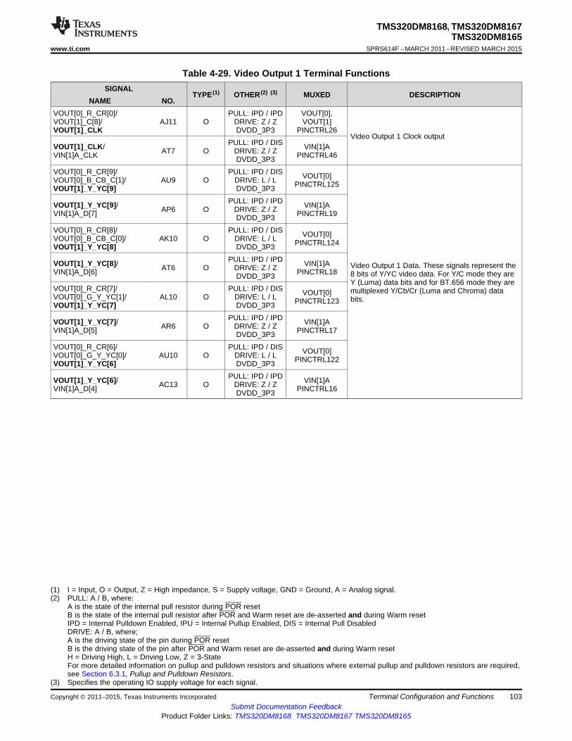
TMS320DM8168, TMS320DM8167TMS320DM8165
www.ti.com SPRS614F –MARCH 2011–REVISED MARCH 2015
Table 4-29. Video Output 1 Terminal FunctionsSIGNAL
TYPE (1) OTHER (2) (3) MUXED DESCRIPTIONNAME NO.
VOUT[0]_R_CR[0]/ PULL: IPD / IPD VOUT[0],VOUT[1]_C[8]/ AJ11 O DRIVE: Z / Z VOUT[1]VOUT[1]_CLK DVDD_3P3 PINCTRL26
Video Output 1 Clock outputPULL: IPD / DISVOUT[1]_CLK/ VIN[1]AAT7 O DRIVE: Z / ZVIN[1]A_CLK PINCTRL46DVDD_3P3
VOUT[0]_R_CR[9]/ PULL: IPD / DIS VOUT[0]VOUT[0]_B_CB_C[1]/ AU9 O DRIVE: L / L PINCTRL125VOUT[1]_Y_YC[9] DVDD_3P3PULL: IPD / IPDVOUT[1]_Y_YC[9]/ VIN[1]AAP6 O DRIVE: Z / ZVIN[1]A_D[7] PINCTRL19DVDD_3P3
VOUT[0]_R_CR[8]/ PULL: IPD / DIS VOUT[0]VOUT[0]_B_CB_C[0]/ AK10 O DRIVE: L / L PINCTRL124VOUT[1]_Y_YC[8] DVDD_3P3PULL: IPD / IPDVOUT[1]_Y_YC[8]/ VIN[1]A Video Output 1 Data. These signals represent theAT6 O DRIVE: Z / ZVIN[1]A_D[6] PINCTRL18 8 bits of Y/YC video data. For Y/C mode they areDVDD_3P3
Y (Luma) data bits and for BT.656 mode they areVOUT[0]_R_CR[7]/ PULL: IPD / DIS multiplexed Y/Cb/Cr (Luma and Chroma) dataVOUT[0]VOUT[0]_G_Y_YC[1]/ AL10 O DRIVE: L / L bits.PINCTRL123VOUT[1]_Y_YC[7] DVDD_3P3
PULL: IPD / IPDVOUT[1]_Y_YC[7]/ VIN[1]AAR6 O DRIVE: Z / ZVIN[1]A_D[5] PINCTRL17DVDD_3P3VOUT[0]_R_CR[6]/ PULL: IPD / DIS VOUT[0]VOUT[0]_G_Y_YC[0]/ AU10 O DRIVE: L / L PINCTRL122VOUT[1]_Y_YC[6] DVDD_3P3
PULL: IPD / IPDVOUT[1]_Y_YC[6]/ VIN[1]AAC13 O DRIVE: Z / ZVIN[1]A_D[4] PINCTRL16DVDD_3P3
(1) I = Input, O = Output, Z = High impedance, S = Supply voltage, GND = Ground, A = Analog signal.(2) PULL: A / B, where:
A is the state of the internal pull resistor during POR resetB is the state of the internal pull resistor after POR and Warm reset are de-asserted and during Warm resetIPD = Internal Pulldown Enabled, IPU = Internal Pullup Enabled, DIS = Internal Pull DisabledDRIVE: A / B, where;A is the driving state of the pin during POR resetB is the driving state of the pin after POR and Warm reset are de-asserted and during Warm resetH = Driving High, L = Driving Low, Z = 3-StateFor more detailed information on pullup and pulldown resistors and situations where external pullup and pulldown resistors are required,see Section 6.3.1, Pullup and Pulldown Resistors.
(3) Specifies the operating IO supply voltage for each signal.
Copyright © 2011–2015, Texas Instruments Incorporated Terminal Configuration and Functions 103Submit Documentation Feedback
Product Folder Links: TMS320DM8168 TMS320DM8167 TMS320DM8165

TMS320DM8168, TMS320DM8167TMS320DM8165SPRS614F –MARCH 2011–REVISED MARCH 2015 www.ti.com
Table 4-29. Video Output 1 Terminal Functions (continued)SIGNAL
TYPE (1) OTHER (2) (3) MUXED DESCRIPTIONNAME NO.
VOUT[0]_R_CR[5]/ PULL: IPD / DIS VOUT[0]VOUT[0]_AVID/ AT10 O DRIVE: L / L PINCTRL121VOUT[1]_Y_YC[5] DVDD_3P3PULL: IPD / DISVOUT[1]_Y_YC[5]/ VIN[1]AAJ7 O DRIVE: Z / ZVIN[1]A_D[3] PINCTRL50DVDD_3P3
VOUT[0]_R_CR[4]/ PULL: IPD / DIS VOUT[0]VOUT[0]_FLD/ AG13 O DRIVE: L / L PINCTRL120VOUT[1]_Y_YC[4] DVDD_3P3PULL: IPD / DISVOUT[1]_Y_YC[4]/ VIN[1]A Video Output 1 Data. These signals represent theAU6 O DRIVE: Z / ZVIN[1]A_D[2] PINCTRL49 8 bits of Y/YC video data. For Y/C mode they areDVDD_3P3
Y (Luma) data bits and for BT.656 mode they areVOUT[0]_R_CR[3]/ PULL: IPD / DIS multiplexed Y/Cb/Cr (Luma and Chroma) dataVOUT[0]VOUT[0]_VSYNC / AR11 O DRIVE: L / L bits.PINCTRL119VOUT[1]_Y_YC[3] DVDD_3P3
PULL: IPD / DISVOUT[1]_Y_YC[3] VIN[1]AAP7 O DRIVE: Z / ZVIN[1]A_D[1] PINCTRL48DVDD_3P3VOUT[0]_R_CR[2]/ PULL: IPD / DIS VOUT[0]VOUT[0]_HSYNC/ AT11 O DRIVE: L / L PINCTRL118VOUT[1]_Y_YC[2] DVDD_3P3
PULL: IPD / DISVOUT[1]_Y_YC[2]/ VIN[1]AAU7 O DRIVE: Z / ZVIN[1]A_D[0] PINCTRL47DVDD_3P3VOUT[0]_B_CB_C[0]/ PULL: IPD / IPD VOUT[0],VOUT[1]_C[9]/ AR9 O DRIVE: Z / Z VIN[1]BVIN[1]B_HSYNC_DE DVDD_3P3 PINCTRL27VIN[0]A_D[19]/ PULL: IPD / IPD VIN[0]A,VIN[1]A_DE/ AK4 O DRIVE: Z / Z VIN[1]AVOUT[1]_C[9] DVDD_3P3VIN[0]A_D[18]/ PULL: IPD / IPD VIN[0]A,VIN[1]A_FLD/ AK5 O DRIVE: Z / Z VIN[1]AVOUT[1]_C[8] DVDD_3P3 PINCTRL24VOUT[0]_R_CR[0]/ PULL: IPD / IPD VOUT[0],VOUT[1]_C[8]/ AJ11 O DRIVE: Z / Z VOUT[1]VOUT[1]_CLK DVDD_3P3 PINCTRL26
PULL: IPD / IPDVOUT[1]_C[7]/ VIN[1]AAD13 O DRIVE: Z / Z Video Output 1 Data. These signals represent theVIN[1]A_D[13] PINCTRL10DVDD_3P3 8 bits of C video data. For Y/C mode they aremultiplexed Cb/Cr (Chroma) data bits, and forPULL: IPD / IPDVOUT[1]_C[6]/ VIN[1]A BT.656 mode they are unused.AN8 O DRIVE: Z / ZVIN[1]A_D[12] PINCTRL9DVDD_3P3
PULL: IPD / IPDVOUT[1]_C[5]/ VIN[1]AAP8 O DRIVE: Z / ZVIN[1]A_D[11] PINCTRL8DVDD_3P3PULL: IPD / IPDVOUT[1]_C[4]/ VIN[1]AAN7 O DRIVE: Z / ZVIN[1]A_D[10] PINCTRL7DVDD_3P3PULL: IPD / IPDVOUT[1]_C[3]/ VIN[1]AAM8 O DRIVE: Z / ZVIN[1]A_D[9]/ PINCTRL6DVDD_3P3PULL: IPD / IPDVOUT[1]_C[2]/ VIN[1]AAK6 O DRIVE: Z / ZVIN[1]A_D[8] PINCTRL20DVDD_3P3
104 Terminal Configuration and Functions Copyright © 2011–2015, Texas Instruments IncorporatedSubmit Documentation Feedback
Product Folder Links: TMS320DM8168 TMS320DM8167 TMS320DM8165

TMS320DM8168, TMS320DM8167TMS320DM8165
www.ti.com SPRS614F –MARCH 2011–REVISED MARCH 2015
Table 4-29. Video Output 1 Terminal Functions (continued)SIGNAL
TYPE (1) OTHER (2) (3) MUXED DESCRIPTIONNAME NO.
VIN[0]A_D[16]/ PULL: IPD / IPD VIN[0]A,VIN[1]A_HSYNC/ AT5 O DRIVE: Z / Z VIN[1]A
Video Output 1 Field ID output. This is the discreteVOUT[1]_FLD DVDD_3P3 PINCTRL22field identification output. This signal is not used
VOUT[0]_G_Y_YC[1]/ PULL: IPD / IPD VOUT[0], for embedded sync modes.VOUT[1]_FLD/ AU8 O DRIVE: Z / Z VIN[1]BVIN[1]B_FLD DVDD_3P3 PINCTRL30VOUT[0]_B_CB_C[1]/VOUT[1]_HSYNC PULL: IPD / IPD VOUT[0],(silicon revision 1.x) AT9 O DRIVE: Z / Z VOUT[1]DAC_VOUT[1]_HSYNC Video Output 1 Active Video output. This is theDVDD_3P3 PINCTRL28(silicon revision 2.x)/ discrete active video indicator output. This signalVOUT[1]_AVID is not used for embedded sync modes.
PULL: IPD / IPDVOUT[1]_AVID/ VIN[1]BAT4 O DRIVE: Z / ZVIN[1]B_CLK PINCTRL31DVDD_3P3
Table 4-30. Video Output 1 [Pins AT9, AR5, AP9, AL5] Terminal FunctionsSIGNAL
TYPE (1) OTHER (2) (3) MUXED DESCRIPTIONNAME NO.
Silicon Revision 1.x DevicesVOUT[0]_B_CB_C[1]/ PULL: IPD / IPD VOUT[0],VOUT[1]_HSYNC/ AT9 O DRIVE: Z / Z VOUT[1]
Video Output 1 Horizontal Sync output. This is theVOUT[1]_AVID DVDD_3P3 PINCTRL28discrete horizontal synchronization output. This
PULL: IPD / IPD signal is not used for embedded sync modes.VOUT[1]_HSYNC/ VIN[1]AAR5 O DRIVE: Z / ZVIN[1]A_D[15] PINCTRL21DVDD_3P3VOUT[0]_G_Y_YC[0]/ PULL: IPD / IPD VOUT[0],VOUT[1]_VSYNC/ AP9 O DRIVE: Z / Z VIN[1]B
Video Output 1 Vertical Sync output. This is theVIN[1]B_VSYNC DVDD_3P3 PINCTRL29discrete vertical synchronization output. This
VIN[0]A_D[17]/ PULL: IPD / IPD VIN[0]A, signal is not used for embedded sync modes.VIN[1]A_VSYNC/ AL5 O DRIVE: Z / Z VIN[1]AVOUT[1]_VSYNC DVDD_3P3 PINCTRL23Silicon Revision 2.x DevicesVOUT[0]_B_CB_C[1]/ PULL: IPD / IPD VOUT[0], Pin supports two functions in silicon revision 2.xDAC_VOUT[1]_HSYNC/ AT9 O DRIVE: Z / Z VOUT[1] devices:VOUT[1]_AVID DVDD_3P3 PINCTRL28 1. Video Output 1 Horizontal Sync output. This is
the discrete horizontal synchronization output.This signal is not used for embedded syncmodes.PULL: IPD / IPDDAC_VOUT[1]_HSYNC/ VIN[1]AAR5 O DRIVE: Z / Z 2. Discrete Horizontal Sync for HD-DACs.VIN[1]A_D[15] PINCTRL21DVDD_3P3
Functionality is set in SPARE_CTRL0 register asdefined in Section 9.10.
(1) I = Input, O = Output, Z = High impedance, S = Supply voltage, GND = Ground, A = Analog signal.(2) PULL: A / B, where:
A is the state of the internal pull resistor during POR resetB is the state of the internal pull resistor after POR and Warm reset are de-asserted and during Warm resetIPD = Internal Pulldown Enabled, IPU = Internal Pullup Enabled, DIS = Internal Pull DisabledDRIVE: A / B, where;A is the driving state of the pin during POR resetB is the driving state of the pin after POR and Warm reset are de-asserted and during Warm resetH = Driving High, L = Driving Low, Z = 3-StateFor more detailed information on pullup and pulldown resistors and situations where external pullup and pulldown resistors are required,see Section 6.3.1, Pullup and Pulldown Resistors.
(3) Specifies the operating IO supply voltage for each signal.
Copyright © 2011–2015, Texas Instruments Incorporated Terminal Configuration and Functions 105Submit Documentation Feedback
Product Folder Links: TMS320DM8168 TMS320DM8167 TMS320DM8165
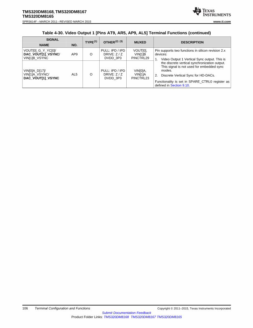
TMS320DM8168, TMS320DM8167TMS320DM8165SPRS614F –MARCH 2011–REVISED MARCH 2015 www.ti.com
Table 4-30. Video Output 1 [Pins AT9, AR5, AP9, AL5] Terminal Functions (continued)SIGNAL
TYPE (1) OTHER (2) (3) MUXED DESCRIPTIONNAME NO.
VOUT[0]_G_Y_YC[0]/ PULL: IPD / IPD VOUT[0], Pin supports two functions in silicon revision 2.xDAC_VOUT[1]_VSYNC/ AP9 O DRIVE: Z / Z VIN[1]B devices:VIN[1]B_VSYNC DVDD_3P3 PINCTRL29 1. Video Output 1 Vertical Sync output. This is
the discrete vertical synchronization output.This signal is not used for embedded syncmodes.VIN[0]A_D[17]/ PULL: IPD / IPD VIN[0]A,
VIN[1]A_VSYNC/ AL5 O DRIVE: Z / Z VIN[1]A 2. Discrete Vertical Sync for HD-DACs.DAC_VOUT[1]_VSYNC DVDD_3P3 PINCTRL23
Functionality is set in SPARE_CTRL0 register asdefined in Section 9.10.
106 Terminal Configuration and Functions Copyright © 2011–2015, Texas Instruments IncorporatedSubmit Documentation Feedback
Product Folder Links: TMS320DM8168 TMS320DM8167 TMS320DM8165

TMS320DM8168, TMS320DM8167TMS320DM8165
www.ti.com SPRS614F –MARCH 2011–REVISED MARCH 2015
4.2.21 Analog Video Output Signals
Table 4-31. Analog Video Output Terminal FunctionsSIGNAL
TYPE (1) OTHER DESCRIPTIONNAME NO.
When a specific Video DAC output [IOUTA - IOUTG] is powered down, the corresponding Analog Video Output terminal functionsshould be left unconnected.IOUTA AT21 O - Video DAC A output. Analog HD Video DAC (G/Y)IOUTB AR21 O - Video DAC B output. Analog HD Video DAC (B/Pb)IOUTC AP21 O - Video DAC C output. Analog HD Video DAC (R/Pr)IOUTD AR20 O - Video DAC D output. Analog SD Video DACIOUTE AT19 O - Video DAC E output. Analog SD Video DACIOUTF AT20 O - Video DAC F output. Analog SD Video DACIOUTG AU20 O - Video DAC G output. Analog SD Video DACDAC_VOUT[1]_HSYNC, AR5,DAC_HSYNC_ AT9, O - Analog HD Video DAC Discrete HSYNC OutputVOUT[0]_AVID AR8DAC_VOUT[1]_VSYNC, AL5,DAC_VSYNC_ O - Analog HD Video DAC Discrete VSYNC OutputAP9, AL9VOUT[0]_FLD
Video DAC reference voltage (0.5 V).VDAC_VREF AH19 I - When the video DACs are powered down, this pin should be left
unconnected.Video DAC HD current bias connection. This pin must be connectedvia an external 1.2-kΩ resistor to VSSA_HD.
VDAC_RBIAS_HD AE22 IO -When the HD DACs are powered down, this pin should be leftunconnected.Video DAC SD current bias connection. This pin must be connectedvia an external 1.2-kΩ resistor to VSSA_SD.
VDAC_RBIAS_SD AP19 IO -When the SD DACs are powered down, this pin should be leftunconnected.
(1) I = Input, O = Output, Z = High impedance, S = Supply voltage, GND = Ground, A = Analog signal.
Copyright © 2011–2015, Texas Instruments Incorporated Terminal Configuration and Functions 107Submit Documentation Feedback
Product Folder Links: TMS320DM8168 TMS320DM8167 TMS320DM8165
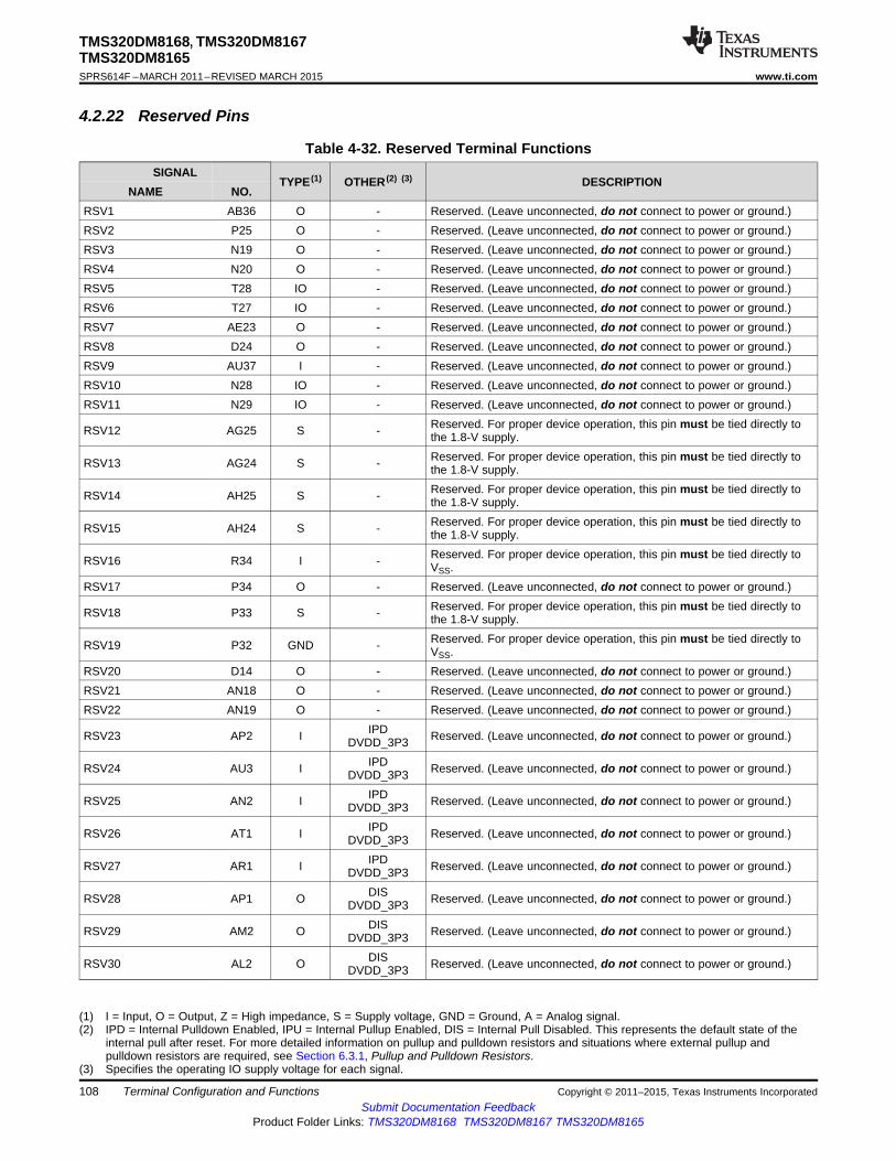
TMS320DM8168, TMS320DM8167TMS320DM8165SPRS614F –MARCH 2011–REVISED MARCH 2015 www.ti.com
4.2.22 Reserved Pins
Table 4-32. Reserved Terminal FunctionsSIGNAL
TYPE (1) OTHER (2) (3) DESCRIPTIONNAME NO.
RSV1 AB36 O - Reserved. (Leave unconnected, do not connect to power or ground.)RSV2 P25 O - Reserved. (Leave unconnected, do not connect to power or ground.)RSV3 N19 O - Reserved. (Leave unconnected, do not connect to power or ground.)RSV4 N20 O - Reserved. (Leave unconnected, do not connect to power or ground.)RSV5 T28 IO - Reserved. (Leave unconnected, do not connect to power or ground.)RSV6 T27 IO - Reserved. (Leave unconnected, do not connect to power or ground.)RSV7 AE23 O - Reserved. (Leave unconnected, do not connect to power or ground.)RSV8 D24 O - Reserved. (Leave unconnected, do not connect to power or ground.)RSV9 AU37 I - Reserved. (Leave unconnected, do not connect to power or ground.)RSV10 N28 IO - Reserved. (Leave unconnected, do not connect to power or ground.)RSV11 N29 IO - Reserved. (Leave unconnected, do not connect to power or ground.)
Reserved. For proper device operation, this pin must be tied directly toRSV12 AG25 S - the 1.8-V supply.Reserved. For proper device operation, this pin must be tied directly toRSV13 AG24 S - the 1.8-V supply.Reserved. For proper device operation, this pin must be tied directly toRSV14 AH25 S - the 1.8-V supply.Reserved. For proper device operation, this pin must be tied directly toRSV15 AH24 S - the 1.8-V supply.Reserved. For proper device operation, this pin must be tied directly toRSV16 R34 I - VSS.
RSV17 P34 O - Reserved. (Leave unconnected, do not connect to power or ground.)Reserved. For proper device operation, this pin must be tied directly toRSV18 P33 S - the 1.8-V supply.Reserved. For proper device operation, this pin must be tied directly toRSV19 P32 GND - VSS.
RSV20 D14 O - Reserved. (Leave unconnected, do not connect to power or ground.)RSV21 AN18 O - Reserved. (Leave unconnected, do not connect to power or ground.)RSV22 AN19 O - Reserved. (Leave unconnected, do not connect to power or ground.)
IPDRSV23 AP2 I Reserved. (Leave unconnected, do not connect to power or ground.)DVDD_3P3IPDRSV24 AU3 I Reserved. (Leave unconnected, do not connect to power or ground.)DVDD_3P3IPDRSV25 AN2 I Reserved. (Leave unconnected, do not connect to power or ground.)DVDD_3P3IPDRSV26 AT1 I Reserved. (Leave unconnected, do not connect to power or ground.)DVDD_3P3IPDRSV27 AR1 I Reserved. (Leave unconnected, do not connect to power or ground.)DVDD_3P3DISRSV28 AP1 O Reserved. (Leave unconnected, do not connect to power or ground.)DVDD_3P3DISRSV29 AM2 O Reserved. (Leave unconnected, do not connect to power or ground.)DVDD_3P3DISRSV30 AL2 O Reserved. (Leave unconnected, do not connect to power or ground.)DVDD_3P3
(1) I = Input, O = Output, Z = High impedance, S = Supply voltage, GND = Ground, A = Analog signal.(2) IPD = Internal Pulldown Enabled, IPU = Internal Pullup Enabled, DIS = Internal Pull Disabled. This represents the default state of the
internal pull after reset. For more detailed information on pullup and pulldown resistors and situations where external pullup andpulldown resistors are required, see Section 6.3.1, Pullup and Pulldown Resistors.
(3) Specifies the operating IO supply voltage for each signal.
108 Terminal Configuration and Functions Copyright © 2011–2015, Texas Instruments IncorporatedSubmit Documentation Feedback
Product Folder Links: TMS320DM8168 TMS320DM8167 TMS320DM8165

TMS320DM8168, TMS320DM8167TMS320DM8165
www.ti.com SPRS614F –MARCH 2011–REVISED MARCH 2015
Table 4-32. Reserved Terminal Functions (continued)SIGNAL
TYPE (1) OTHER (2) (3) DESCRIPTIONNAME NO.
DISRSV31 AK1 O Reserved. (Leave unconnected, do not connect to power or ground.)DVDD_3P3DISRSV32 AL1 O Reserved. (Leave unconnected, do not connect to power or ground.)DVDD_3P3IPDRSV33 AM29 I Reserved. (Leave unconnected, do not connect to power or ground.)DVDD_3P3IPDRSV34 AL28 I Reserved. (Leave unconnected, do not connect to power or ground.)DVDD_3P3IPDRSV35 AL29 I Reserved. (Leave unconnected, do not connect to power or ground.)DVDD_3P3IPDRSV36 AN29 I Reserved. (Leave unconnected, do not connect to power or ground.)DVDD_3P3IPDRSV37 AP29 I Reserved. (Leave unconnected, do not connect to power or ground.)DVDD_3P3DISRSV38 AR29 O Reserved. (Leave unconnected, do not connect to power or ground.)DVDD_3P3DISRSV39 AT29 O Reserved. (Leave unconnected, do not connect to power or ground.)DVDD_3P3DISRSV40 AT28 O Reserved. (Leave unconnected, do not connect to power or ground.)DVDD_3P3
RSV41 AU21 O - Reserved. (Leave unconnected, do not connect to power or ground.)IPURSV42 AJ1 IO Reserved. (Leave unconnected, do not connect to power or ground.)DVDD_3P3IPURSV43 AK2 IO Reserved. (Leave unconnected, do not connect to power or ground.)DVDD_3P3DISRSV44 AH8 O Reserved. (Leave unconnected, do not connect to power or ground.)DVDD_3P3DISRSV45 AJ2 O Reserved. (Leave unconnected, do not connect to power or ground.)DVDD_3P3DISRSV46 AK3 O Reserved. (Leave unconnected, do not connect to power or ground.)DVDD_3P3DISRSV47 AJ3 O Reserved. (Leave unconnected, do not connect to power or ground.)DVDD_3P3IPDRSV48 AJ4 I Reserved. (Leave unconnected, do not connect to power or ground.)DVDD_3P3IPDRSV49 AJ5 I Reserved. (Leave unconnected, do not connect to power or ground.)DVDD_3P3IPDRSV50 AJ6 I Reserved. (Leave unconnected, do not connect to power or ground.)DVDD_3P3IPDRSV51 AB13 I Reserved. (Leave unconnected, do not connect to power or ground.)DVDD_3P3
Reserved. For proper device operation, this pin should be connected to aRSV52 AE21 S - 1.0-V power supply.Reserved. For proper device operation, this pin should be connected to aRSV53 AG22 S - 1.8-V power supply.Reserved. For proper device operation, this pin should be connected to aRSV54 AG23 S - 1.8-V power supply.Reserved. For proper device operation, this pin should be connected to aRSV55 AH23 S - 1.8-V power supply.Reserved. For proper device operation, this pin should be connected to aRSV56 AJ23 S - 1.8-V power supply.
AK22 Reserved. For proper device operation, this pin must be tied directly toRSV57 GND - VSS.AL22 Reserved. For proper device operation, this pin must be tied directly toRSV58 GND - VSS.
Copyright © 2011–2015, Texas Instruments Incorporated Terminal Configuration and Functions 109Submit Documentation Feedback
Product Folder Links: TMS320DM8168 TMS320DM8167 TMS320DM8165
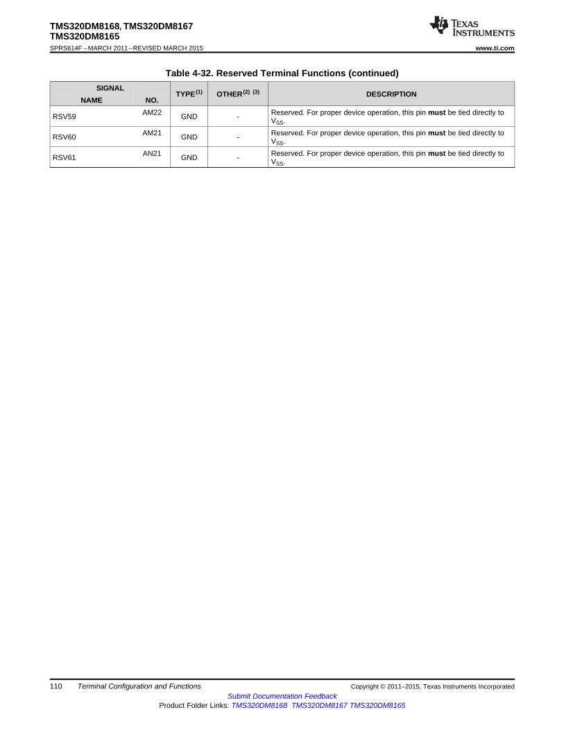
TMS320DM8168, TMS320DM8167TMS320DM8165SPRS614F –MARCH 2011–REVISED MARCH 2015 www.ti.com
Table 4-32. Reserved Terminal Functions (continued)SIGNAL
TYPE (1) OTHER (2) (3) DESCRIPTIONNAME NO.
AM22 Reserved. For proper device operation, this pin must be tied directly toRSV59 GND - VSS.AM21 Reserved. For proper device operation, this pin must be tied directly toRSV60 GND - VSS.AN21 Reserved. For proper device operation, this pin must be tied directly toRSV61 GND - VSS.
110 Terminal Configuration and Functions Copyright © 2011–2015, Texas Instruments IncorporatedSubmit Documentation Feedback
Product Folder Links: TMS320DM8168 TMS320DM8167 TMS320DM8165

TMS320DM8168, TMS320DM8167TMS320DM8165
www.ti.com SPRS614F –MARCH 2011–REVISED MARCH 2015
4.2.23 Supply Voltages
Table 4-33. Supply Terminal FunctionsSIGNAL
TYPE (1) OTHER DESCRIPTIONNAME NO.
Reference Power Supply DDR[0]:VREFSSTL_DDR[0] A17 S - • 0.75-V for DDR3 memory type
• 0.9-V for DDR2 memory typeReference Power Supply DDR[1]
VREFSSTL_DDR[1] A21 S - • 0.75-V for DDR3 memory type• 0.9-V for DDR2 memory type
AD22, AD21,AD20, AD19,AD18, AD17,AD16, AC22,AC21, AC20,AC19, AC18,AC17, AC16,AB24, AB23,AB22, AB21,AB20, AB19,
CVDD AB18, AB17, S - Variable Core Voltage Supply for the Always ON DomainAB16, AB15,AB14, T24,
T23, T22, T21,T20, T19, T18,T17, T16, T15,T14, R22, R21,R20, R19, R18,R17, R16, P22,P21, P20, P19,P18, P17, P16AE25, AE13,AD24, AD23,AD15, AD14,AC24, AC23,
CVDDC AC15, AC14, S - 1.0-V Constant Power Supply for Memories and PLLsR24, R23, R15,R14, P24, P23,P15, P14, N25,
N130.9-V Power Supply for USB PHYs.
VDD_USB_0P9 N27 S - Note: If the USB is not used, for proper device operation, this pinmust be connected to a power supply (0.9 V or CVDDC).1.0-V Power Supply for SATA Termination and Analog Front EndY34, Y33, V34,VDDT_SATA S - Note: If the SATA is not used, for proper device operation, theseV32 pins must be connected to a 1.0-V power supply.1.0-V Power Supply for PCIe Termination and Analog Front EndY30, Y28, AB32,VDDT_PCIE S - Note: If the PCIe is not used, these pins should be connected toAB29, AB27 a 1.0-V power supply.
VDDA_PLL B18, A18 S - 1.5-V Analog Power Supply for PLLsAR27, AP24, 1.0-V Analog Power Supply for HDMI
VDDA_HDMI AP23, S - Note: If the HDMI is not used, these pins should be connected toAN24, AN23 a 1.0-V power supply.
1.0-V Analog Power Supply for VDAC HD DACVDDA_HD_1P0 AG21 S - Note: If the HD DAC is not used, this pin should be connected to
a 1.0-V power supply.1.0-V Analog Power Supply for VDAC SD DAC
VDDA_SD_1P0 AG20 S - Note: If the SD DAC is not used, this pin should be connected toa 1.0-V power supply.1.5-V Regulator Power Supply for SATA
VDDR_SATA V25, U25 S - Note: If the SATA is not used, for proper device operation, thesepins must be connected to a 1.5-V power supply.
(1) I = Input, O = Output, Z = High impedance, S = Supply voltage, GND = Ground, A = Analog signal.
Copyright © 2011–2015, Texas Instruments Incorporated Terminal Configuration and Functions 111Submit Documentation Feedback
Product Folder Links: TMS320DM8168 TMS320DM8167 TMS320DM8165

TMS320DM8168, TMS320DM8167TMS320DM8165SPRS614F –MARCH 2011–REVISED MARCH 2015 www.ti.com
Table 4-33. Supply Terminal Functions (continued)SIGNAL
TYPE (1) OTHER DESCRIPTIONNAME NO.
1.5-V Regulator Power Supply for PCIeVDDR_PCIE Y25, W25 S - Note: If the PCIe is not used, for proper device operation, these
pins must be connected to a 1.5-V power supply.L19, L18, L17,L16, L15, L14,
Power Supply for DDR[0] IOs:K19, K18, K17,DVDD_DDR[0] K16, K15, K14, S - • 1.5-V for DDR3 memory type
J18, J17, J16, • 1.8-V for DDR2 memory typeJ15, J14, E11,A11, E1, A2
L24, L23, L22,L21, L20, K24,
1.5-V Power Supply for DDR[1] IOs:K23, K22, K21,DVDD_DDR[1] K20, J24, J23, S - • 1.5-V for DDR3 memory type
J22, J21, J20, • 1.8-V for DDR2 memory typeJ19, E27, D37,
A36, A271.8-V Power Supply for Device Oscillator
DEVOSC_DVDD18 E19 S - Note: If the oscillator is not used, this pin should be connected tothe 1.8-V power supply (DVDD1P8).1.8-V Power Supply for USB0Note: If the USB is not used, for proper device operation, this pinVDD_USB0_1P8 R25 S - must be connected to a 1.8-V power supply, or when the USBPHY is not used, this pin can be optionally connected to CVDDC.1.8-V Power Supply for USB1Note: If the USB is not used, for proper device operation, this pinVDD_USB1_1P8 T25 S - must be connected to a 1.8-V power supply, or when the USBPHY is not used, this pin can be optionally connected to CVDDC.
DVDD1P8 AJ20, AJ24 S - 1.8-V Power Supply1.8-V Reference Power Supply for VDAC
VDDA_REF_1P8 AT22 S - Note: If the VDAC is not used, these pins should be connectedto a 1.8-V power supply.1.8-V Analog Power Supply for VDAC HD DAC
VDDA_HD_1P8 AJ22, AH22 S - Note: If the HD DAC is not used, these pins should beconnected to a 1.8-V power supply.1.8-V Analog Power Supply for VDAC SD DACAJ21, AH21,VDDA_SD_1P8 S - Note: If the SD DAC is not used, these pins should be connectedAH20 to a 1.8-V power supply.
112 Terminal Configuration and Functions Copyright © 2011–2015, Texas Instruments IncorporatedSubmit Documentation Feedback
Product Folder Links: TMS320DM8168 TMS320DM8167 TMS320DM8165
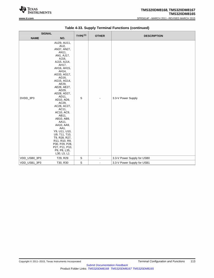
TMS320DM8168, TMS320DM8167TMS320DM8165
www.ti.com SPRS614F –MARCH 2011–REVISED MARCH 2015
Table 4-33. Supply Terminal Functions (continued)SIGNAL
TYPE (1) OTHER DESCRIPTIONNAME NO.
AU29, AU11,AU2,
AN37, AN27,AN11,
AN1, AJ17,AJ16,
AJ15, AJ14,AH17,
AH16, AH15,AH14,
AG33, AG17,AG16,
AG15, AG14,AE29,
AE28, AE27,AD29,
AD28, AD27,AD11,DVDD_3P3 S - 3.3-V Power SupplyAD10, AD9,AC29,
AC28, AC27,AC11,
AC10, AC9,AB11,
AB10, AB9,AA11,
AA10, AA9,AA1,
Y9, U11, U10,U9, T11, T10,T9, R28, R27,R11, R10, R9,P30, P29, P28,P27, P11, P10,
P9, P8, L35,L30, L5, L1
VDD_USB0_3P3 T29, R29 S - 3.3-V Power Supply for USB0VDD_USB1_3P3 T30, R30 S - 3.3-V Power Supply for USB1
Copyright © 2011–2015, Texas Instruments Incorporated Terminal Configuration and Functions 113Submit Documentation Feedback
Product Folder Links: TMS320DM8168 TMS320DM8167 TMS320DM8165

TMS320DM8168, TMS320DM8167TMS320DM8165SPRS614F –MARCH 2011–REVISED MARCH 2015 www.ti.com
4.2.24 Ground Pins (VSS)
Table 4-34. Ground Terminal FunctionsSIGNAL
TYPE (1) OTHER DESCRIPTIONNAME NO.
AU28, AU23, AU12,AU1, AT23, AR25,AR24, AR23, AR15,AP37, AP15, AN15,AN14, AM31, AM25,AM24, AM23, AM19,AM18, AM17, AM16,AM15, AM7, AM1,AL32, AL31, AL24,AL23, AL19, AL18,AL17, AL16, AL15,AL7, AL6, AK27, AK24,AK23, AK19, AK18,AK17, AK16, AK15,AK11, AJ25, AJ18,AG30, AG26, AG12,AG8, AG5, AF27,AF11, AE20, AE19,AE18, AE17, AD34,VSS GND - Ground (GND)AD33, AD32, AD31,AD30, AD7, AD6, AD5,AC34, AC33, AC32,AC31, AC30, AC8,AC7, AC6, AC4, AC3,AB37, AB35, AB8, AB7,AB6, AB1, AA24, AA23,AA22, AA21, AA20,AA19, AA18, AA17,AA16, AA15, AA14,AA13, AA8, AA7, AA6,AA5, Y37, Y36, Y32,Y31, Y24, Y23, Y22,Y21, Y20, Y19, Y18,Y17, Y16, Y15, Y14,Y13, Y8, Y7, Y6, Y5,Y4, W24, W23, W22,W21, W20, W19, W18,W17, W16
(1) I = Input, O = Output, Z = High impedance, S = Supply voltage, GND = Ground, A = Analog signal.
114 Terminal Configuration and Functions Copyright © 2011–2015, Texas Instruments IncorporatedSubmit Documentation Feedback
Product Folder Links: TMS320DM8168 TMS320DM8167 TMS320DM8165

TMS320DM8168, TMS320DM8167TMS320DM8165
www.ti.com SPRS614F –MARCH 2011–REVISED MARCH 2015
Table 4-34. Ground Terminal Functions (continued)SIGNAL
TYPE (1) OTHER DESCRIPTIONNAME NO.
W15, W14, W13, W9,W8, W7, W6, V28, V27,V24, V23, V22, V21,V20, V19, V18, V17,V16, V15, V14, V13,V9, V8, V7, V6, V5, V4,U24, U23, U22, U21,U20, U18, U17, U16,U15, U14, U13, U8, U7,U6, U5, T35, T34, T33,T8, T7, T6, R33, R32,R31, R8, R7, R6, R4,R3, P31, P7, P6, P5,P4, N18, M27, M11,VSS GND - Ground (GND)L33, L26, L12, L8, K37,K1, H27, H24, H23,H22, H21, H20, H19,H18, H17, H16, H15,H14, H11, G32, G31,G24, G23, G22, G21,G20, G18, G17, G16,G15, G14, G7, G6,F31, F24, F23, F22,F21, F17, F16, F15,F14, F7, E37, E24,E14, D1, C23, C21,C17, C15, A37, A28,A10, A1
VSSA_PLL U19, B20, A20 GND - Analog GND for PLLsVSSA_HD AK21, AK20, AL21 GND - Analog GND for VDAC HD DAC
AU19, AM20, AN20,VSSA_SD GND - Analog GND for VDAC SD DACAL20VSSA_REF_1P8 AU22 GND - Reference GND for VDAC (1.8 V)DEVOSC_VSS B19 GND - Ground for Device Oscillator
Copyright © 2011–2015, Texas Instruments Incorporated Terminal Configuration and Functions 115Submit Documentation Feedback
Product Folder Links: TMS320DM8168 TMS320DM8167 TMS320DM8165
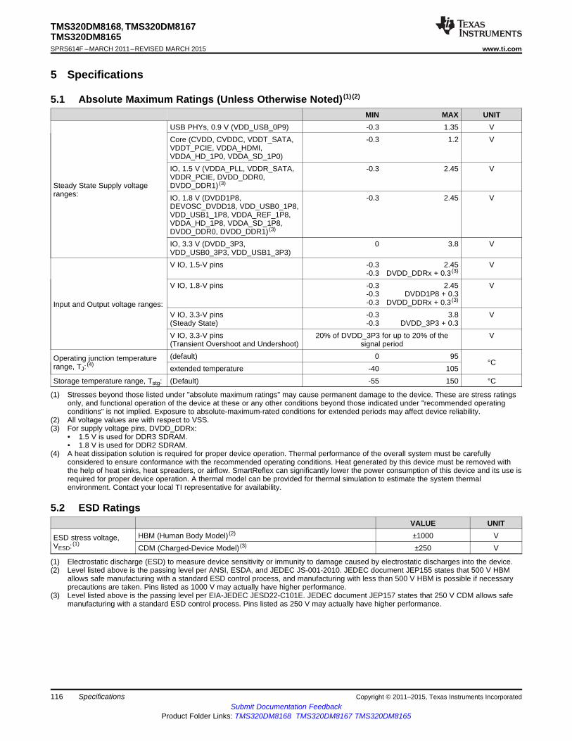
TMS320DM8168, TMS320DM8167TMS320DM8165SPRS614F –MARCH 2011–REVISED MARCH 2015 www.ti.com
5 Specifications
5.1 Absolute Maximum Ratings (Unless Otherwise Noted) (1) (2)
MIN MAX UNITUSB PHYs, 0.9 V (VDD_USB_0P9) -0.3 1.35 VCore (CVDD, CVDDC, VDDT_SATA, -0.3 1.2 VVDDT_PCIE, VDDA_HDMI,VDDA_HD_1P0, VDDA_SD_1P0)IO, 1.5 V (VDDA_PLL, VDDR_SATA, -0.3 2.45 VVDDR_PCIE, DVDD_DDR0,
Steady State Supply voltage DVDD_DDR1) (3)
ranges: IO, 1.8 V (DVDD1P8, -0.3 2.45 VDEVOSC_DVDD18, VDD_USB0_1P8,VDD_USB1_1P8, VDDA_REF_1P8,VDDA_HD_1P8, VDDA_SD_1P8,DVDD_DDR0, DVDD_DDR1) (3)
IO, 3.3 V (DVDD_3P3, 0 3.8 VVDD_USB0_3P3, VDD_USB1_3P3)V IO, 1.5-V pins -0.3 2.45 V
-0.3 DVDD_DDRx + 0.3 (3)
V IO, 1.8-V pins -0.3 2.45 V-0.3 DVDD1P8 + 0.3-0.3 DVDD_DDRx + 0.3 (3)Input and Output voltage ranges:
V IO, 3.3-V pins -0.3 3.8 V(Steady State) -0.3 DVDD_3P3 + 0.3V IO, 3.3-V pins 20% of DVDD_3P3 for up to 20% of the V(Transient Overshoot and Undershoot) signal period(default) 0 95Operating junction temperature °Crange, TJ: (4) extended temperature -40 105
Storage temperature range, Tstg: (Default) -55 150 °C
(1) Stresses beyond those listed under "absolute maximum ratings" may cause permanent damage to the device. These are stress ratingsonly, and functional operation of the device at these or any other conditions beyond those indicated under "recommended operatingconditions" is not implied. Exposure to absolute-maximum-rated conditions for extended periods may affect device reliability.
(2) All voltage values are with respect to VSS.(3) For supply voltage pins, DVDD_DDRx:
• 1.5 V is used for DDR3 SDRAM.• 1.8 V is used for DDR2 SDRAM.
(4) A heat dissipation solution is required for proper device operation. Thermal performance of the overall system must be carefullyconsidered to ensure conformance with the recommended operating conditions. Heat generated by this device must be removed withthe help of heat sinks, heat spreaders, or airflow. SmartReflex can significantly lower the power consumption of this device and its use isrequired for proper device operation. A thermal model can be provided for thermal simulation to estimate the system thermalenvironment. Contact your local TI representative for availability.
5.2 ESD RatingsVALUE UNIT
HBM (Human Body Model) (2) ±1000 VESD stress voltage,VESD: (1) CDM (Charged-Device Model) (3) ±250 V
(1) Electrostatic discharge (ESD) to measure device sensitivity or immunity to damage caused by electrostatic discharges into the device.(2) Level listed above is the passing level per ANSI, ESDA, and JEDEC JS-001-2010. JEDEC document JEP155 states that 500 V HBM
allows safe manufacturing with a standard ESD control process, and manufacturing with less than 500 V HBM is possible if necessaryprecautions are taken. Pins listed as 1000 V may actually have higher performance.
(3) Level listed above is the passing level per EIA-JEDEC JESD22-C101E. JEDEC document JEP157 states that 250 V CDM allows safemanufacturing with a standard ESD control process. Pins listed as 250 V may actually have higher performance.
116 Specifications Copyright © 2011–2015, Texas Instruments IncorporatedSubmit Documentation Feedback
Product Folder Links: TMS320DM8168 TMS320DM8167 TMS320DM8165

TMS320DM8168, TMS320DM8167TMS320DM8165
www.ti.com SPRS614F –MARCH 2011–REVISED MARCH 2015
5.3 Recommended Operating ConditionsMIN NOM MAX UNIT
Supply voltage, Variable Initial Startup VINITnom × 0.95 1.00 or 1.05 (2) VINITnom × 1.05Core, Adaptive VoltageCVDD CYGA2 & CYG4 SRnom (3) × 0.95 0.85 - 1.00 SRnom × 1.05 VScaling (CVDD) (1)
CYG & CYG2 SRnom × 0.95 0.85-1.05 (4) SRnom × 1.05Supply voltage, Constant Core (CVDDC,
CVDDC VDDT_SATA, VDDT_PCIE, VDDA_HDMI, 0.95 1 1.05 VVDDA_HD_1P0, VDDA_SD_1P0)Supply voltage, IO, 3.3 V (DVDD_3P3,VDD_USB0_3P3, VDD_USB1_3P3) 3.13 3.3 3.47 V(except I2C pins)Supply voltage, IO, I2C (DVDD_3P3) 3.13 3.3 3.47 VSupply voltage, IO, 1.8 V (DVDD1P8,DEVOSC_DVDD18, VDD_USB0_1P8,
DVDD VDD_USB1_1P8, VDDA_REF_1P8, 1.71 1.8 1.89 VVDDA_HD_1P8, VDDA_SD_1P8, DVDD_DDR0,DVDD_DDR1) (5)
Supply voltage, IO, 1.5 V (VDDA_PLL,VDDR_SATA, VDDR_PCIE, DVDD_DDR0, 1.43 1.5 1.58 VDVDD_DDR1) (5)
Supply voltage, IO, 0.9 V (VDD_USB_0P9) 0.85 0.9 0.95 VSupply ground (VSS, VSSA_PLL, VSSA_HD,VSS 0 0 0 VVSSA_SD, VSSA_REF_1P8, DEVOSC_VSS) (6)
DDR_VREF DDR2 and DDR3 reference voltage (7) 0.48DVDD_DDRx 0.5DVDD_DDRx 0.52DVDD_DDRx VHigh-level input voltage, 3.3 V (except I2C pins) 2
VIH High-level input voltage, I2C 0.7DVDD_3P3 VHigh-level input voltage, 1.8 V 0.65DVDD1P8Low-level input voltage, 3.3 V (except I2C pins) 0.8
VIL Low-level input voltage, I2C 0.3DVDD_3P3 VLow-level input voltage, 1.8 V 0.35DVDD1P8High-level output current 6-mA IO buffers -6
DDR[0], DDR[1]IOH mAbuffers @ 50-Ω -8impedance setting
Low-level output current 6-mA IO buffers 6DDR[0], DDR[1]IOL mAbuffers @ 50-Ω 8impedance setting
Differential input voltage (SERDES_CLKN and 0.25VID 2.0 VSERDES_CLKP), [AC coupled]
(1) This device supports, and requires the use of, SmartReflex technology with Adaptive Voltage Scaling based on die temperature andperformance. The SmartReflex codes output from the device correspond to up to 32 linear voltage steps within the specified voltagerange (32 steps is the recommended software upper limit and is not constrained by the silicon design), with the option to use fewersteps if desired, with a minimum of eight steps. TI requires that users design a supply that can handle multiple voltage steps within thisrange with ± 5% tolerances. Not incorporating a flexible supply may limit the system's ability to use the power saving capabilities of theSmartReflex technology. TI recommends using a fault-tolerant power supply design to protect against over-current conditions. For moredetails about adaptive voltage scaling for this device, see the AVS FAQ. For AVS disable data to aid in design of robust power suppliesthat may withstand momentary AVS control failure, see the device Power Estimation Spreadsheet (literature number SPRABK3).
(2) The initial CVDD voltage at power on must be 1.00V nominal (for CYGA2 and CYG4 devices) or 1.05V nominal (for CYG and CYG2devices) and it must transition to the AVS target value adjusted by a AVS driver. This is required to maintain full power functionality andreliability targets specified by TI.
(3) SRnom refers to the unique SmartReflex core supply voltage set from the factory for each individual device.(4) Upper range limit of 1.10 nominal value allowed.(5) For supply voltage pins, DVDD_DDRx:
• 1.5 V is used for DDR3 SDRAM.• 1.8 V is used for DDR2 SDRAM.
(6) Oscillator ground (DEVOSC_VSS) must be kept separate from other grounds and connected directly to the crystal load capacitorground.
(7) DDR_VREF is expected to equal 0.5DVDD_DDRx of the transmitting device and to track variations in the DVDD_DDRx.
Copyright © 2011–2015, Texas Instruments Incorporated Specifications 117Submit Documentation Feedback
Product Folder Links: TMS320DM8168 TMS320DM8167 TMS320DM8165

TMS320DM8168, TMS320DM8167TMS320DM8165SPRS614F –MARCH 2011–REVISED MARCH 2015 www.ti.com
Recommended Operating Conditions (continued)MIN NOM MAX UNIT
Transition time, 10%-90%, All Inputs (unless Lesser of 0.25P ortt nsotherwise specified in the electrical data sections) 10 (8)
Operating junction temperature range (9) 0 95TJ °C
Extended operating junction temperature range -40 105
(8) P = the period of the applied signal. Maintaining transition times as fast as possible is recommended to improve noise immunity on inputsignals.
(9) A heat dissipation solution is required for proper device operation. Thermal performance of the overall system must be carefullyconsidered to ensure conformance with the recommended operating conditions. Heat generated by this device must be removed withthe help of heat sinks, heat spreaders, or airflow. SmartReflex can significantly lower the power consumption of this device and its use isrequired for proper device operation. A thermal model can be provided for thermal simulation to estimate the system thermalenvironment. Contact your local TI representative for availability.
118 Specifications Copyright © 2011–2015, Texas Instruments IncorporatedSubmit Documentation Feedback
Product Folder Links: TMS320DM8168 TMS320DM8167 TMS320DM8165
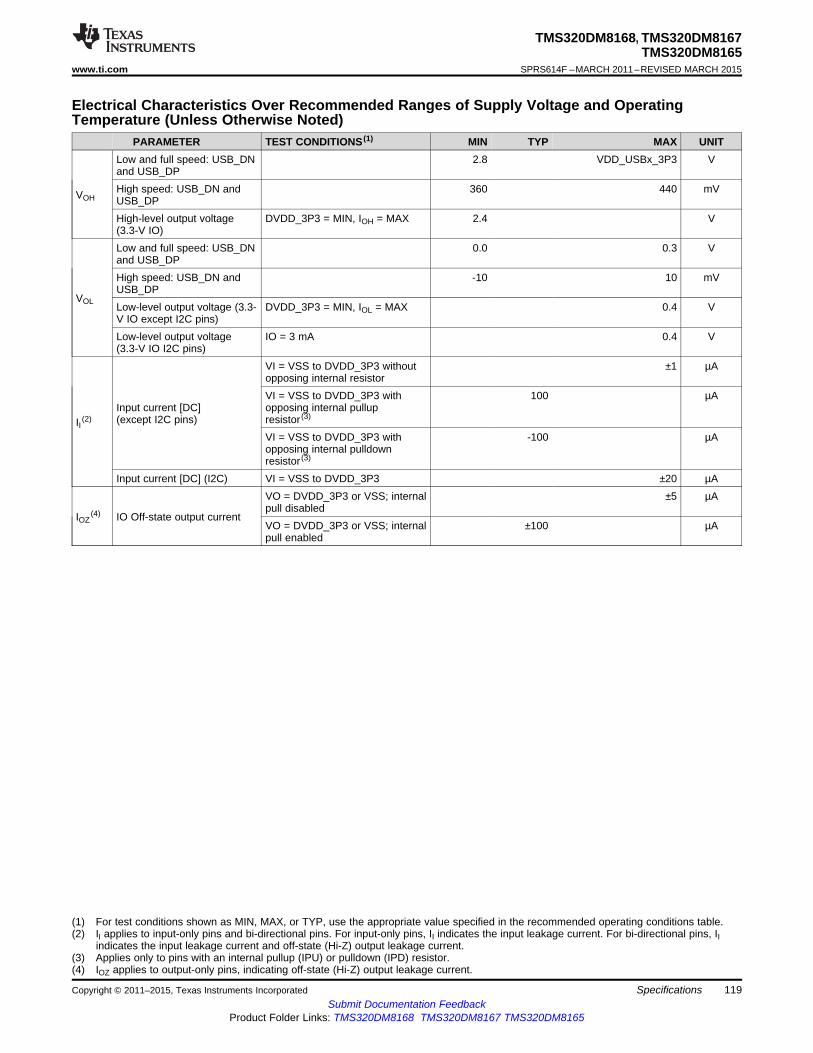
TMS320DM8168, TMS320DM8167TMS320DM8165
www.ti.com SPRS614F –MARCH 2011–REVISED MARCH 2015
Electrical Characteristics Over Recommended Ranges of Supply Voltage and OperatingTemperature (Unless Otherwise Noted)
PARAMETER TEST CONDITIONS (1) MIN TYP MAX UNITLow and full speed: USB_DN 2.8 VDD_USBx_3P3 Vand USB_DPHigh speed: USB_DN and 360 440 mVVOH USB_DPHigh-level output voltage DVDD_3P3 = MIN, IOH = MAX 2.4 V(3.3-V IO)Low and full speed: USB_DN 0.0 0.3 Vand USB_DPHigh speed: USB_DN and -10 10 mVUSB_DP
VOL Low-level output voltage (3.3- DVDD_3P3 = MIN, IOL = MAX 0.4 VV IO except I2C pins)Low-level output voltage IO = 3 mA 0.4 V(3.3-V IO I2C pins)
VI = VSS to DVDD_3P3 without ±1 µAopposing internal resistorVI = VSS to DVDD_3P3 with 100 µA
Input current [DC] opposing internal pullup(except I2C pins) resistor (3)II (2)
VI = VSS to DVDD_3P3 with -100 µAopposing internal pulldownresistor (3)
Input current [DC] (I2C) VI = VSS to DVDD_3P3 ±20 µAVO = DVDD_3P3 or VSS; internal ±5 µApull disabled
IOZ(4) IO Off-state output current
VO = DVDD_3P3 or VSS; internal ±100 µApull enabled
(1) For test conditions shown as MIN, MAX, or TYP, use the appropriate value specified in the recommended operating conditions table.(2) II applies to input-only pins and bi-directional pins. For input-only pins, II indicates the input leakage current. For bi-directional pins, II
indicates the input leakage current and off-state (Hi-Z) output leakage current.(3) Applies only to pins with an internal pullup (IPU) or pulldown (IPD) resistor.(4) IOZ applies to output-only pins, indicating off-state (Hi-Z) output leakage current.
Copyright © 2011–2015, Texas Instruments Incorporated Specifications 119Submit Documentation Feedback
Product Folder Links: TMS320DM8168 TMS320DM8167 TMS320DM8165

TMS320DM8168, TMS320DM8167TMS320DM8165SPRS614F –MARCH 2011–REVISED MARCH 2015 www.ti.com
Electrical Characteristics Over Recommended Ranges of Supply Voltage and OperatingTemperature (Unless Otherwise Noted) (continued)
PARAMETER TEST CONDITIONS (1) MIN TYP MAX UNITmA• Case Temp = 60ºC
• ARM at 1.2 GHz, 75%utilizationConstant Core (CVDDC) 1491 (6)
supply current (5) • DSP at 1 GHz, 25%utilization
• HDVICP2-0 at 600 MHz, 1-ch1080p60 encode
ICDD • HDVICP2-1 at 600 MHz, 1-ch1080p60 decode
• HDMI displayVariable Core (CVDD) supply • SGX530 at 150 MHz, 15 fps 6463 (6)current (5)
• EMIF0 and EMIF1 at 800MHz, 4480 MBps
• USB 1x, EMAC 1x, SATAmA• Case Temp = 60ºC
3.3-V IO (DVDD_3P3, • ARM at 1.2 GHz, 75%USB_VDDA3P3) supply 19 (6)utilizationcurrent (5)
• DSP at 1 GHz, 25%utilization
• HDVICP2-0 at 600 MHz, 1-ch1080p60 encode
1.8-V IO (DVDD1P8,IDDD • HDVICP2-1 at 600 MHz, 1-chDVDD_DDRx) supply 11 (6)1080p60 decodecurrent (5) (7)
• HDMI display• SGX530 at 150 MHz, 15 fps• EMIF0 and EMIF1 at 8001.5-V IO (DVDD_DDRx) 1241 (6)MHz, 4480 MBpssupply current (5) (7)
• USB 1x, EMAC 1x, SATACI Input capacitance 2.8 pFCo Output capacitance 2.8 pF
(5) The actual current draw varies across manufacturing processes and is highly application-dependent. For use-case specific powerestimates, see the device Power Estimation Spreadsheet (literature number SPRABK3).
(6) The ICDD and IDDD TYP power values shown in this table correspond to device speed grade 2 (CYG2).(7) For supply voltage pins, DVDD_DDRx:
• 1.5 V is used for DDR3 SDRAM.• 1.8 V is used for DDR2 SDRAM.
5.4 Thermal Resistance Characteristics
Table 5-1. Thermal Resistance Characteristics (PBGA Package) [CYG]NO. °C/W (1)
1 RΘJC Junction-to-case 0.212 RΘJB Junction-to-board 3.93
(1) For proper device operation, a heatsink is required.
120 Specifications Copyright © 2011–2015, Texas Instruments IncorporatedSubmit Documentation Feedback
Product Folder Links: TMS320DM8168 TMS320DM8167 TMS320DM8165

TMS320DM8168, TMS320DM8167TMS320DM8165
www.ti.com SPRS614F –MARCH 2011–REVISED MARCH 2015
6 Device Configurations
6.1 Control ModuleThe device control module includes status and control logic not addressed within the peripherals or theremainder of the device infrastructure. This module is the primary point of control for the following areas ofthe device:• Functional IO multiplexing• Device status• Static device configuration• Open-core protocol (OCP) interface for standard and customer programmable e-Fuse bit shift
registers.
The control module primarily implements a bank of registers accessible (read and write) by the softwarealong with some read-only registers carrying status information. Most register bits are exported as controlsignals for other logic blocks on the device. Certain control module registers have default values basedupon the device type as decoded from e-Fuse.
The read and write registers can be divided into the following classes:• Static device configuration registers• Status and configuration registers• Boot registers
Table 6-1 shows the general register groupings and Table 6-2 through Table 6-4 provide registersummaries for each group.
Table 6-1. Control Module Register Map
ADDRESS OFFSET REGISTER GROUP SEE0x0000 - 0x0020 OCP Configuration registers Table 6-20x0024 - 0x003C Reserved0x0040 – 0x00FC Device Boot registers Table 6-70x0300 - 0x03FC Reserved0x0400 - 0x05FC PLL Control registers Table 6-30x0600 - 0x07FC Device Configuration registers Table 6-40x0800 - 0x0FFC PAD Control registers Section 6.5
Table 6-2. OCP Configuration Registers Summary
HEX ADDRESS ACRONYM REGISTER NAME0x4814 0000 CONTROL_REVISION Control module Revision number
0x4814 0004 - 0x4814 000C - Reserved0x4814 0010 CONTROL_SYSCONFIG Idle mode parameters
0x4814 0014 - 0x4814 003C - Reserved
Table 6-3. PLL Control Registers Summary
HEX ADDRESS ACRONYM REGISTER NAME0x4814 0400 MAINPLL_CTRL Main PLL base frequency control0x4814 0404 MAINPLL_PWD Main PLL clock output powerdown0x4814 0408 MAINPLL_FREQ1 Main Clock 1 fractional divider0x4814 040C MAINPLL_DIV1 Main Clock 1 post divider0x4814 0410 MAINPLL_FREQ2 Main Clock 2 fractional divider0x4814 0414 MAINPLL_DIV2 Main Clock 2 post divider
Copyright © 2011–2015, Texas Instruments Incorporated Device Configurations 121Submit Documentation Feedback
Product Folder Links: TMS320DM8168 TMS320DM8167 TMS320DM8165
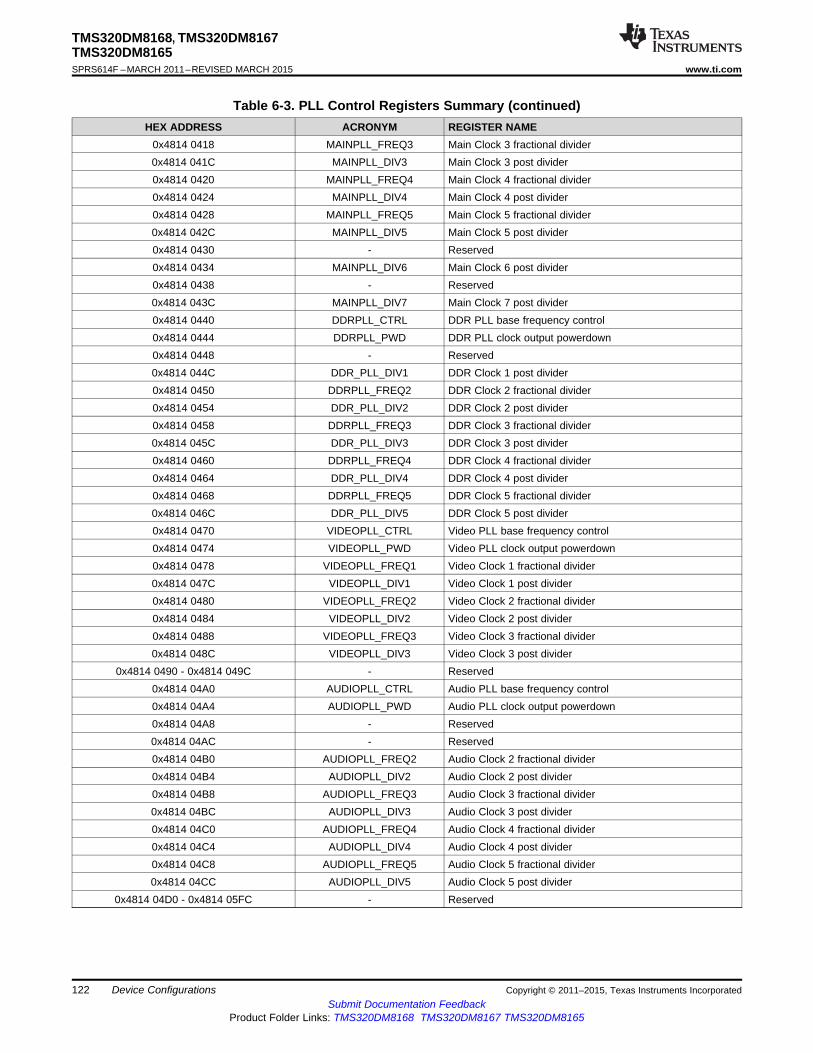
TMS320DM8168, TMS320DM8167TMS320DM8165SPRS614F –MARCH 2011–REVISED MARCH 2015 www.ti.com
Table 6-3. PLL Control Registers Summary (continued)HEX ADDRESS ACRONYM REGISTER NAME
0x4814 0418 MAINPLL_FREQ3 Main Clock 3 fractional divider0x4814 041C MAINPLL_DIV3 Main Clock 3 post divider0x4814 0420 MAINPLL_FREQ4 Main Clock 4 fractional divider0x4814 0424 MAINPLL_DIV4 Main Clock 4 post divider0x4814 0428 MAINPLL_FREQ5 Main Clock 5 fractional divider0x4814 042C MAINPLL_DIV5 Main Clock 5 post divider0x4814 0430 - Reserved0x4814 0434 MAINPLL_DIV6 Main Clock 6 post divider0x4814 0438 - Reserved0x4814 043C MAINPLL_DIV7 Main Clock 7 post divider0x4814 0440 DDRPLL_CTRL DDR PLL base frequency control0x4814 0444 DDRPLL_PWD DDR PLL clock output powerdown0x4814 0448 - Reserved0x4814 044C DDR_PLL_DIV1 DDR Clock 1 post divider0x4814 0450 DDRPLL_FREQ2 DDR Clock 2 fractional divider0x4814 0454 DDR_PLL_DIV2 DDR Clock 2 post divider0x4814 0458 DDRPLL_FREQ3 DDR Clock 3 fractional divider0x4814 045C DDR_PLL_DIV3 DDR Clock 3 post divider0x4814 0460 DDRPLL_FREQ4 DDR Clock 4 fractional divider0x4814 0464 DDR_PLL_DIV4 DDR Clock 4 post divider0x4814 0468 DDRPLL_FREQ5 DDR Clock 5 fractional divider0x4814 046C DDR_PLL_DIV5 DDR Clock 5 post divider0x4814 0470 VIDEOPLL_CTRL Video PLL base frequency control0x4814 0474 VIDEOPLL_PWD Video PLL clock output powerdown0x4814 0478 VIDEOPLL_FREQ1 Video Clock 1 fractional divider0x4814 047C VIDEOPLL_DIV1 Video Clock 1 post divider0x4814 0480 VIDEOPLL_FREQ2 Video Clock 2 fractional divider0x4814 0484 VIDEOPLL_DIV2 Video Clock 2 post divider0x4814 0488 VIDEOPLL_FREQ3 Video Clock 3 fractional divider0x4814 048C VIDEOPLL_DIV3 Video Clock 3 post divider
0x4814 0490 - 0x4814 049C - Reserved0x4814 04A0 AUDIOPLL_CTRL Audio PLL base frequency control0x4814 04A4 AUDIOPLL_PWD Audio PLL clock output powerdown0x4814 04A8 - Reserved0x4814 04AC - Reserved0x4814 04B0 AUDIOPLL_FREQ2 Audio Clock 2 fractional divider0x4814 04B4 AUDIOPLL_DIV2 Audio Clock 2 post divider0x4814 04B8 AUDIOPLL_FREQ3 Audio Clock 3 fractional divider0x4814 04BC AUDIOPLL_DIV3 Audio Clock 3 post divider0x4814 04C0 AUDIOPLL_FREQ4 Audio Clock 4 fractional divider0x4814 04C4 AUDIOPLL_DIV4 Audio Clock 4 post divider0x4814 04C8 AUDIOPLL_FREQ5 Audio Clock 5 fractional divider0x4814 04CC AUDIOPLL_DIV5 Audio Clock 5 post divider
0x4814 04D0 - 0x4814 05FC - Reserved
122 Device Configurations Copyright © 2011–2015, Texas Instruments IncorporatedSubmit Documentation Feedback
Product Folder Links: TMS320DM8168 TMS320DM8167 TMS320DM8165

TMS320DM8168, TMS320DM8167TMS320DM8165
www.ti.com SPRS614F –MARCH 2011–REVISED MARCH 2015
Table 6-4. Device Configuration Registers Summary
HEX ADDRESS ACRONYM REGISTER NAME0x4814 0600 DEVICE_ID Device Identification0x4814 0604 - Reserved0x4814 0608 INIT_PRESSURE_0 L3 Initiator Pressure0x4814 060C INIT_PRESSURE_1 L3 Initiator Pressure0x4814 0610 MMU_CFG System MMU Configuration0x4814 0614 TPTC_CFG Transfer Controller Configuration0x4814 0618 DDR_CTRL DDR Interface Control0x4814 061C DSP_IDLE_CFG DSP Standby and Idle Management Configuration0x4814 0620 USB_CTRL USB Control0x4814 0624 USBPHY_CTRL0 USB0 Phy Control0x4814 0628 - Reserved0x4814 062C USBPHY_CTRL1 USB1 Phy Control0x4814 0630 MAC_ID0_LO Ethernet MAC Address 00x4814 0634 MAC_ID0_HI Ethernet MAC Address 00x4814 0638 MAC_ID1_LO Ethernet MAC Address 10x4814 063C MAC_ID1_HI Ethernet MAC Address 10x4814 0640 PCIE_CFG PCIe Module Configuration0x4814 0644 - Reserved0x4814 0648 CLK_CTRL Input Oscillator Control0x4814 064C AUDIO_CTRL Audio Control0x4814 0650 DSPMEM_SLEEP DSP Memory Sleep Mode Configuration0x4814 0654 OCMEM_SLEEP On-Chip Memory Sleep Mode Configuration
0x4814 0658 - 0x4814 065C - Reserved0x4814 0660 HD_DAC_CTRL HD DAC Control0x4814 0664 HD_DACA_CAL HD DAC A Calibration0x4814 0668 HD_DACB_CAL HD DAC B Calibration0x4814 066C HD_DACC_CAL HD DAC C Calibration0x4814 0670 SD_DAC_CTRL SD DAC Control0x4814 0674 SD_DACA_CAL SD DAC A Calibration0x4814 0678 SD_DACB_CAL SD DAC B Calibration0x4814 067C SD_DACC_CAL SD DAC C Calibration0x4814 0680 SD_DACD_CAL SD DAC D Calibration
0x4814 0684 - 0x4814 0688 - Reserved0x4814 068C BANDGAP_CTRL DAC Band-gap Control0x4814 0690 HW_EVT_SEL_GRP1 System Trace Hardware Event Select Group 10x4814 0694 HW_EVT_SEL_GRP2 System Trace Hardware Event Select Group 20x4814 0698 HW_EVT_SEL_GRP3 System Trace Hardware Event Select Group 30x4814 069C HW_EVT_SEL_GRP4 System Trace Hardware Event Select Group 4
0x4814 06A0 - 0x4814 06F4 - Reserved0x4814 06F8 HDMI_OBSCLK_CTRL HDMI Observe Clock Control0x4814 06FC SERDES_CTRL Serdes Control0x4814 0700 UCB_CLK_CTL USB Clock Control0x4814 0704 PLL_OBSCLK_CTRL PLL Observe Clock Control0x4814 0708 - Reserved0x4814 070C DDR_RCD RCD Power Enable or Disable
0x4814 0710 - 0x4814 07FC - Reserved
Copyright © 2011–2015, Texas Instruments Incorporated Device Configurations 123Submit Documentation Feedback
Product Folder Links: TMS320DM8168 TMS320DM8167 TMS320DM8165
TMS320DM8168, TMS320DM8167TMS320DM8165SPRS614F –MARCH 2011–REVISED MARCH 2015 www.ti.com
6.2 Revision IdentificationThe silicon revision can be read in the DEVREV bit field value of the device identification (DEVICE_ID)register (located at 0x4814 0600). The DEVREV field of the DEVICE_ID register changes between siliconrevisions. Table 6-5 lists the contents of the device revision (DEVREV) field value for each revision of thedevice.
Table 6-5. Device Revision (DEVREV) Bit Field Value
DEVICE REVISION FIELD VALUESILICON REVISION DEVREV[31:28]2.1 00112.0 00101.1 00011.0 0000
More details on the DEVICE_ID register can be found in the TMS320DM816x DaVinci Digital MediaProcessors Technical Reference Manual (literature number SPRUGX8).
6.3 Debugging Considerations
6.3.1 Pullup and Pulldown ResistorsProper board design should ensure that input pins to the device always be at a valid logic level and notfloating. This may be achieved via pullup and pulldown resistors. The device features internal pullup (IPU)and internal pulldown (IPD) resistors on most pins to eliminate the need, unless otherwise noted, forexternal pullup or pulldown resistors.
An external pullup or pulldown resistor needs to be used in the following situations:• Boot and Configuration Pins: If the pin is both routed out and 3-stated (not driven), an external pullup
or pulldown resistor is strongly recommended, even if the IPU or IPD matches the desired value orstate.
• Other Input Pins: If the IPU or IPD does not match the desired value or state, use an external pullup orpulldown resistor to pull the signal to the opposite rail.
For the boot and configuration pins (listed in Table 4-1, Boot Terminal Functions), if they are both routedout and 3-stated (not driven), it is strongly recommended that an external pullup or pulldown resistor beimplemented. Although, internal pullup and pulldown resistors exist on these pins and they may match thedesired configuration value, providing external connectivity can help ensure that valid logic levels arelatched on these device boot and configuration pins. In addition, applying external pullup or pulldownresistors on the boot and configuration pins adds convenience to the user in debugging and flexibility inswitching operating modes.
Tips for choosing an external pullup or pulldown resistor:• Consider the total amount of current that may pass through the pullup or pulldown resistor. Make sure
to include the leakage currents of all the devices connected to the net, as well as any internal pullup orpulldown resistors.
• Decide a target value for the net. For a pulldown resistor, this should be below the lowest VIL level ofall inputs connected to the net. For a pullup resistor, this should be above the highest VIH level of allinputs on the net. A reasonable choice would be to target the VOL or VOH levels for the logic family ofthe limiting device; which, by definition, have margin to the VIL and VIH levels.
• Select a pullup or pulldown resistor with the largest possible value; but, which can still ensure that thenet will reach the target pulled value when maximum current from all devices on the net is flowingthrough the resistor. The current to be considered includes leakage current plus, any other internal andexternal pullup and pulldown resistors on the net.
124 Device Configurations Copyright © 2011–2015, Texas Instruments IncorporatedSubmit Documentation Feedback
Product Folder Links: TMS320DM8168 TMS320DM8167 TMS320DM8165
TMS320DM8168, TMS320DM8167TMS320DM8165
www.ti.com SPRS614F –MARCH 2011–REVISED MARCH 2015
• For bidirectional nets, there is an additional consideration which sets a lower limit on the resistancevalue of the external resistor. Verify that the resistance is small enough that the weakest output buffercan drive the net to the opposite logic level (including margin).
• Remember to include tolerances when selecting the resistor value.• For pullup resistors, also remember to include tolerances on the DVDD rail.
For most systems, a 1-kΩ resistor can be used to oppose the IPU or IPD while meeting the above criteria.Users should confirm this resistor value is correct for their specific application.
For most systems, a 20-kΩ resistor can be used to compliment the IPU or IPD on the boot andconfiguration pins while meeting the above criteria. Users should confirm this resistor value is correct fortheir specific application.
For most systems, a 20-kΩ resistor can also be used as an external pullup or pulldown on the pins thathave IPUs or IPDs disabled and require an external pullup or pulldown resistor while still meeting theabove criteria. Users should confirm this resistor value is correct for their specific application.
For more detailed information on input current (II), and the low-level or high-level input voltages (VIL andVIH), see , Electrical Characteristics Over Recommended Ranges of Supply Voltage and OperatingTemperature.
For the internal pullup and pulldown resistors for all device pins, see the peripheral-specific or system-specific terminal functions tables in Section 4.2.
6.4 Boot SequenceThe boot sequence is a process by which the device's memory is loaded with program and data sections,and by which some of the device's internal registers are programmed with predetermined values. The bootsequence is started automatically after each device-level global reset. For more details on device-levelglobal resets, see Section 8.2. There are several methods by which the memory and register initializationcan take place. Each of these methods is referred to as a boot mode. The boot mode to be used isselected at reset. The device is booted through multiple means—primary bootloaders within internal ROMor EMIF4, and secondary user bootloaders from peripherals or external memories. The maximum size ofthe boot image is 255KB (ROM uses 1KB internally). Boot modes, pin configurations, and registerconfigurations required for booting the device, are described in the following subsections.
The following boot modes are supported:• NOR Flash boot (muxed and non-muxed, 8-bit or 16-bit)• NAND Flash boot (SLC and MLC with BCH ECC, 8-bit or 16-bit)• SPI boot (EEPROM or Flash, SPI mode 3, 24-bit)• SD boot (SD cards)• EMAC boot (TFTP client)• UART boot (X-modem client)• PCIe boot (client mode, PCIe 32 and PCIe 64).
The state of the device after boot is determined by sampling the input states of the BTMODE[4:0] pinswhen device reset (POR or RESET) is deasserted. The sampled values are latched into theCONTROL_STATUS register, which is part of the system configuration (SYSCFG) module.
The BTMODE [4:0] values determine the boot mode order according to Table 6-6. The first boot modelisted for each BTMODE[4:0] configuration is executed as the primary boot mode. If the primary bootmode fails, the second, third, and fourth boot modes are executed, in that order, until a successful boot iscompleted.
Additional boot configuration pins determine the following system boot settings as shown in Table 4-1:• GPMC CS0 Default Bus Width• GPMC Wait Enable
Copyright © 2011–2015, Texas Instruments Incorporated Device Configurations 125Submit Documentation Feedback
Product Folder Links: TMS320DM8168 TMS320DM8167 TMS320DM8165
TMS320DM8168, TMS320DM8167TMS320DM8165SPRS614F –MARCH 2011–REVISED MARCH 2015 www.ti.com
• GPMC Address and Data Multiplexing.
The GPMC CS0 default operation is determined by the CS0BW, CS0WAIT, and CS0MUX[1:0] inputs.
For more detailed information on booting the device, see the TMS320DM816x DaVinci Digital MediaProcessors Technical Reference Manual (literature number SPRUGX8).
126 Device Configurations Copyright © 2011–2015, Texas Instruments IncorporatedSubmit Documentation Feedback
Product Folder Links: TMS320DM8168 TMS320DM8167 TMS320DM8165
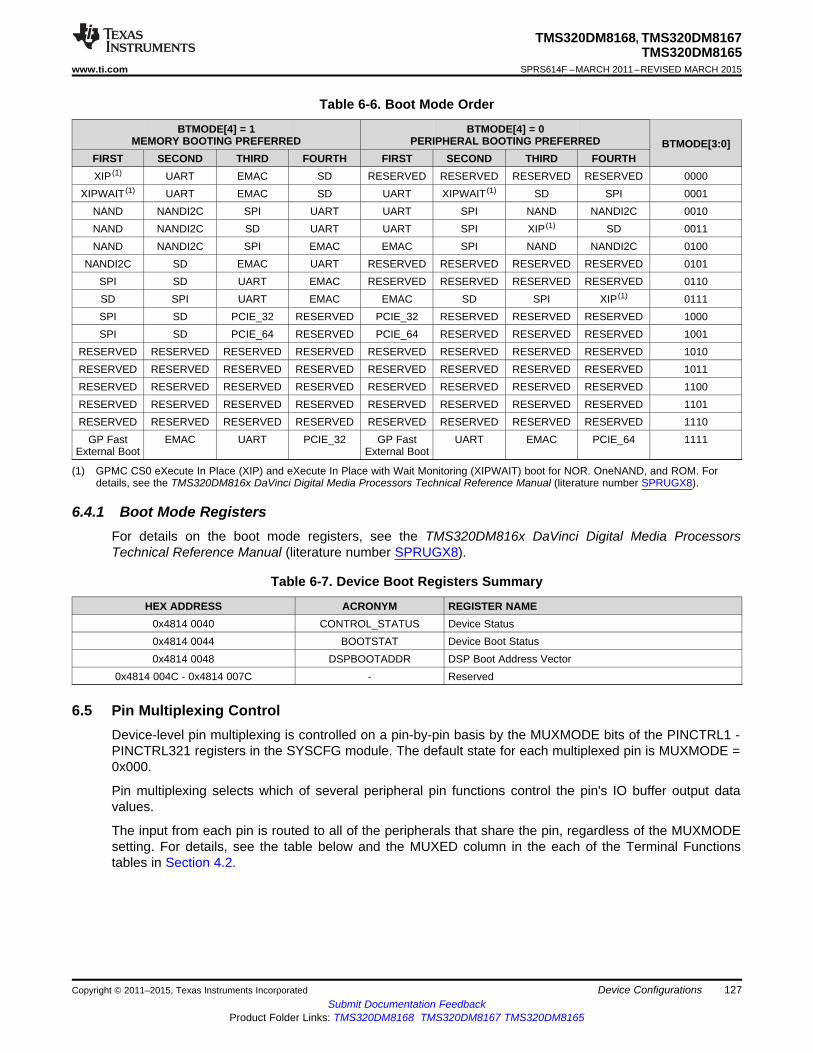
TMS320DM8168, TMS320DM8167TMS320DM8165
www.ti.com SPRS614F –MARCH 2011–REVISED MARCH 2015
Table 6-6. Boot Mode Order
BTMODE[4] = 1 BTMODE[4] = 0MEMORY BOOTING PREFERRED PERIPHERAL BOOTING PREFERRED BTMODE[3:0]
FIRST SECOND THIRD FOURTH FIRST SECOND THIRD FOURTHXIP (1) UART EMAC SD RESERVED RESERVED RESERVED RESERVED 0000
XIPWAIT (1) UART EMAC SD UART XIPWAIT (1) SD SPI 0001NAND NANDI2C SPI UART UART SPI NAND NANDI2C 0010NAND NANDI2C SD UART UART SPI XIP (1) SD 0011NAND NANDI2C SPI EMAC EMAC SPI NAND NANDI2C 0100
NANDI2C SD EMAC UART RESERVED RESERVED RESERVED RESERVED 0101SPI SD UART EMAC RESERVED RESERVED RESERVED RESERVED 0110SD SPI UART EMAC EMAC SD SPI XIP (1) 0111SPI SD PCIE_32 RESERVED PCIE_32 RESERVED RESERVED RESERVED 1000SPI SD PCIE_64 RESERVED PCIE_64 RESERVED RESERVED RESERVED 1001
RESERVED RESERVED RESERVED RESERVED RESERVED RESERVED RESERVED RESERVED 1010RESERVED RESERVED RESERVED RESERVED RESERVED RESERVED RESERVED RESERVED 1011RESERVED RESERVED RESERVED RESERVED RESERVED RESERVED RESERVED RESERVED 1100RESERVED RESERVED RESERVED RESERVED RESERVED RESERVED RESERVED RESERVED 1101RESERVED RESERVED RESERVED RESERVED RESERVED RESERVED RESERVED RESERVED 1110
GP Fast EMAC UART PCIE_32 GP Fast UART EMAC PCIE_64 1111External Boot External Boot
(1) GPMC CS0 eXecute In Place (XIP) and eXecute In Place with Wait Monitoring (XIPWAIT) boot for NOR. OneNAND, and ROM. Fordetails, see the TMS320DM816x DaVinci Digital Media Processors Technical Reference Manual (literature number SPRUGX8).
6.4.1 Boot Mode RegistersFor details on the boot mode registers, see the TMS320DM816x DaVinci Digital Media ProcessorsTechnical Reference Manual (literature number SPRUGX8).
Table 6-7. Device Boot Registers Summary
HEX ADDRESS ACRONYM REGISTER NAME0x4814 0040 CONTROL_STATUS Device Status0x4814 0044 BOOTSTAT Device Boot Status0x4814 0048 DSPBOOTADDR DSP Boot Address Vector
0x4814 004C - 0x4814 007C - Reserved
6.5 Pin Multiplexing ControlDevice-level pin multiplexing is controlled on a pin-by-pin basis by the MUXMODE bits of the PINCTRL1 -PINCTRL321 registers in the SYSCFG module. The default state for each multiplexed pin is MUXMODE =0x000.
Pin multiplexing selects which of several peripheral pin functions control the pin's IO buffer output datavalues.
The input from each pin is routed to all of the peripherals that share the pin, regardless of the MUXMODEsetting. For details, see the table below and the MUXED column in the each of the Terminal Functionstables in Section 4.2.
Copyright © 2011–2015, Texas Instruments Incorporated Device Configurations 127Submit Documentation Feedback
Product Folder Links: TMS320DM8168 TMS320DM8167 TMS320DM8165

TMS320DM8168, TMS320DM8167TMS320DM8165SPRS614F –MARCH 2011–REVISED MARCH 2015 www.ti.com
6.5.1 PINCTRLx Register Descriptions
Table 6-8. PINCTRLx Register DefinitionBit Field Value Description
31:5 Reserved Reserved; Read returns 04 PULLTYPESEL Pad Pullup or Pulldown Type Selection
0 Pulldown selected1 Pullup selected
3 PULLDIS Pad Pullup or Pulldown Disable0 Pullup or Pulldown enabled1 Pullup or Pulldown disabled
2:0 MUXMODE Pad Functional Signal Mux Select
Table 6-9. PINCTRLx Registers
MUXMODE[2:0]HEX ADDRESS REGISTER NAME PULLTYPESEL PULLDIS
000 001 010 011
0x4814 0800 PINCTRL1 0 0
0x4814 0804 PINCTRL2 0 0
0x4814 0808 PINCTRL3 0 0
0x4814 080C PINCTRL4 0 0
0x4814 0810 PINCTRL5 0 0
0x4814 0814 PINCTRL6 0 0 VOUT[1]_C[3] VIN[1]A_D[9]
0x4814 0818 PINCTRL7 0 0 VOUT[1]_C[4] VIN[1]A_D[10]
0x4814 081C PINCTRL8 0 0 VOUT[1]_C[5] VIN[1]A_D[11]
0x4814 0820 PINCTRL9 0 0 VOUT[1]_C[6] VIN[1]A_D[12]
0x4814 0824 PINCTRL10 0 0 VOUT[1]_C[7] VIN[1]A_D[13]
0x4814 0828 PINCTRL11 0 0 VIN[1]A_D[14]
0x4814 082C PINCTRL12 0 0 VIN[0]A_D[20] VIN[0]B_DE
0x4814 0830 PINCTRL13 0 0 VIN[0]A_D[21] VIN[0]B_FLD
0x4814 0834 PINCTRL14 0 0 VIN[0]A_D[22] VIN[0]B_VSYNC
0x4814 0838 PINCTRL15 0 0 VIN[0]A_D[23] VIN[0]B_HSYNC
0x4814 083C PINCTRL16 0 0 VOUT[1]_Y_YC[6] VIN[1]A_D[4]
0x4814 0840 PINCTRL17 0 0 VOUT[1]_Y_YC[7] VIN[1]A_D[5]
0x4814 0844 PINCTRL18 0 0 VOUT[1]_Y_YC[8] VIN[1]A_D[6]
0x4814 0848 PINCTRL19 0 0 VOUT[1]_Y_YC[9] VIN[1]A_D[7]
0x4814 084C PINCTRL20 0 0 VOUT[1]_C[2] VIN[1]A_D[8]
VOUT[1]_HSYNC(silicon revision 1.x)
0x4814 0850 PINCTRL21 0 0 VIN[1]A_D[15]DAC_VOUT[1]_HSYNC
(silicon revision 2.x)
0x4814 0854 PINCTRL22 0 0 VIN[0]A_D[16] VIN[1]A_HSYNC VOUT[1]_FLD
VOUT[1]_VSYNC(silicon revision 1.x)
0x4814 0858 PINCTRL23 0 0 VIN[0]A_D[17] VIN[1]A_VSYNCDAC_VOUT[1]_VSYNC
(silicon revision 2.x)
0x4814 085C PINCTRL24 0 0 VIN[0]A_D[18] VIN[1]A_FLD VOUT[1]_C[8]
0x4814 0860 PINCTRL25 0 0 VIN[0]A_D[19] VIN[1]A_DE VOUT[1]_C[9]
0x4814 0864 PINCTRL26 0 0 VOUT[0]_R_CR[0] VOUT[1]_C[8] VOUT[1]_CLK
0x4814 0868 PINCTRL27 0 0 VOUT[0]_B_CB_C[0] VOUT[1]_C[9] VIN[1]B_HSYNC_DE
VOUT[1]_HSYNC(silicon revision 1.x)
0x4814 086C PINCTRL28 0 0 VOUT[0]_B_CB_C[1] VOUT[1]_AVIDDAC_VOUT[1]_HSYNC
(silicon revision 2.x)
VOUT[1]_VSYNC(silicon revision 1.x)
0x4814 0870 PINCTRL29 0 0 VOUT[0]_G_Y_YC[0] VIN[1]B_VSYNCDAC_VOUT[1]_VSYNC
(silicon revision 2.x)
0x4814 0874 PINCTRL30 0 0 VOUT[0]_G_Y_YC[1] VOUT[1]_FLD VIN[1]B_FLD
128 Device Configurations Copyright © 2011–2015, Texas Instruments IncorporatedSubmit Documentation Feedback
Product Folder Links: TMS320DM8168 TMS320DM8167 TMS320DM8165
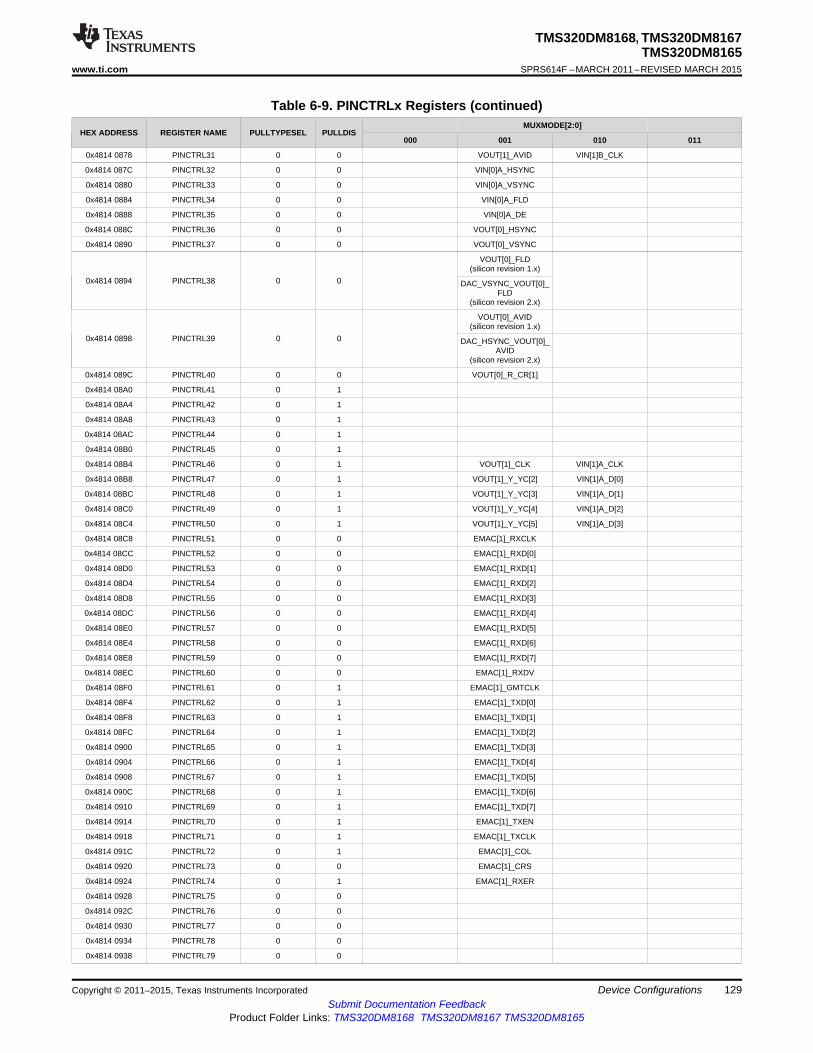
TMS320DM8168, TMS320DM8167TMS320DM8165
www.ti.com SPRS614F –MARCH 2011–REVISED MARCH 2015
Table 6-9. PINCTRLx Registers (continued)MUXMODE[2:0]
HEX ADDRESS REGISTER NAME PULLTYPESEL PULLDIS000 001 010 011
0x4814 0878 PINCTRL31 0 0 VOUT[1]_AVID VIN[1]B_CLK
0x4814 087C PINCTRL32 0 0 VIN[0]A_HSYNC
0x4814 0880 PINCTRL33 0 0 VIN[0]A_VSYNC
0x4814 0884 PINCTRL34 0 0 VIN[0]A_FLD
0x4814 0888 PINCTRL35 0 0 VIN[0]A_DE
0x4814 088C PINCTRL36 0 0 VOUT[0]_HSYNC
0x4814 0890 PINCTRL37 0 0 VOUT[0]_VSYNC
VOUT[0]_FLD(silicon revision 1.x)
0x4814 0894 PINCTRL38 0 0 DAC_VSYNC_VOUT[0]_FLD
(silicon revision 2.x)
VOUT[0]_AVID(silicon revision 1.x)
0x4814 0898 PINCTRL39 0 0 DAC_HSYNC_VOUT[0]_AVID
(silicon revision 2.x)
0x4814 089C PINCTRL40 0 0 VOUT[0]_R_CR[1]
0x4814 08A0 PINCTRL41 0 1
0x4814 08A4 PINCTRL42 0 1
0x4814 08A8 PINCTRL43 0 1
0x4814 08AC PINCTRL44 0 1
0x4814 08B0 PINCTRL45 0 1
0x4814 08B4 PINCTRL46 0 1 VOUT[1]_CLK VIN[1]A_CLK
0x4814 08B8 PINCTRL47 0 1 VOUT[1]_Y_YC[2] VIN[1]A_D[0]
0x4814 08BC PINCTRL48 0 1 VOUT[1]_Y_YC[3] VIN[1]A_D[1]
0x4814 08C0 PINCTRL49 0 1 VOUT[1]_Y_YC[4] VIN[1]A_D[2]
0x4814 08C4 PINCTRL50 0 1 VOUT[1]_Y_YC[5] VIN[1]A_D[3]
0x4814 08C8 PINCTRL51 0 0 EMAC[1]_RXCLK
0x4814 08CC PINCTRL52 0 0 EMAC[1]_RXD[0]
0x4814 08D0 PINCTRL53 0 0 EMAC[1]_RXD[1]
0x4814 08D4 PINCTRL54 0 0 EMAC[1]_RXD[2]
0x4814 08D8 PINCTRL55 0 0 EMAC[1]_RXD[3]
0x4814 08DC PINCTRL56 0 0 EMAC[1]_RXD[4]
0x4814 08E0 PINCTRL57 0 0 EMAC[1]_RXD[5]
0x4814 08E4 PINCTRL58 0 0 EMAC[1]_RXD[6]
0x4814 08E8 PINCTRL59 0 0 EMAC[1]_RXD[7]
0x4814 08EC PINCTRL60 0 0 EMAC[1]_RXDV
0x4814 08F0 PINCTRL61 0 1 EMAC[1]_GMTCLK
0x4814 08F4 PINCTRL62 0 1 EMAC[1]_TXD[0]
0x4814 08F8 PINCTRL63 0 1 EMAC[1]_TXD[1]
0x4814 08FC PINCTRL64 0 1 EMAC[1]_TXD[2]
0x4814 0900 PINCTRL65 0 1 EMAC[1]_TXD[3]
0x4814 0904 PINCTRL66 0 1 EMAC[1]_TXD[4]
0x4814 0908 PINCTRL67 0 1 EMAC[1]_TXD[5]
0x4814 090C PINCTRL68 0 1 EMAC[1]_TXD[6]
0x4814 0910 PINCTRL69 0 1 EMAC[1]_TXD[7]
0x4814 0914 PINCTRL70 0 1 EMAC[1]_TXEN
0x4814 0918 PINCTRL71 0 1 EMAC[1]_TXCLK
0x4814 091C PINCTRL72 0 1 EMAC[1]_COL
0x4814 0920 PINCTRL73 0 0 EMAC[1]_CRS
0x4814 0924 PINCTRL74 0 1 EMAC[1]_RXER
0x4814 0928 PINCTRL75 0 0
0x4814 092C PINCTRL76 0 0
0x4814 0930 PINCTRL77 0 0
0x4814 0934 PINCTRL78 0 0
0x4814 0938 PINCTRL79 0 0
Copyright © 2011–2015, Texas Instruments Incorporated Device Configurations 129Submit Documentation Feedback
Product Folder Links: TMS320DM8168 TMS320DM8167 TMS320DM8165

TMS320DM8168, TMS320DM8167TMS320DM8165SPRS614F –MARCH 2011–REVISED MARCH 2015 www.ti.com
Table 6-9. PINCTRLx Registers (continued)MUXMODE[2:0]
HEX ADDRESS REGISTER NAME PULLTYPESEL PULLDIS000 001 010 011
0x4814 093C PINCTRL80 0 1
0x4814 0940 PINCTRL81 0 1
0x4814 0944 PINCTRL82 0 1
0x4814 0948 PINCTRL83 0 0 VIN[0]A_CLK
0x4814 094C PINCTRL84 0 0 VIN[0]B_CLK
0x4814 0950 PINCTRL85 0 0 VIN[0]A_D[0]
0x4814 0954 PINCTRL86 0 0 VIN[0]A_D[1]
0x4814 0958 PINCTRL87 0 0 VIN[0]A_D[2]
0x4814 095C PINCTRL88 0 0 VIN[0]A_D[3]
0x4814 0960 PINCTRL89 0 0 VIN[0]A_D[4]
0x4814 0964 PINCTRL90 0 0 VIN[0]A_D[5]
0x4814 0968 PINCTRL91 0 0 VIN[0]A_D[6]
0x4814 096C PINCTRL92 0 0 VIN[0]A_D[7]
0x4814 0970 PINCTRL93 0 0 VIN[0]A_D[8]
0x4814 0974 PINCTRL94 0 0 VIN[0]A_D[9]
0x4814 0978 PINCTRL95 0 0 VIN[0]A_D[10]
0x4814 097C PINCTRL96 0 0 VIN[0]A_D[11]
0x4814 0980 PINCTRL97 0 0 VIN[0]A_D[12]
0x4814 0984 PINCTRL98 0 0 VIN[0]A_D[13]
0x4814 0988 PINCTRL99 0 0 VIN[0]A_D[14]
0x4814 098C PINCTRL100 0 0 VIN[0]A_D[15]
0x4814 0990 PINCTRL101 0 1 VOUT[0]_CLK
0x4814 0994 PINCTRL102 0 1 VOUT[0]_G_Y_YC[2]
0x4814 0998 PINCTRL103 0 1 VOUT[0]_G_Y_YC[3]
0x4814 099C PINCTRL104 0 1 VOUT[0]_G_Y_YC[4]
0x4814 09A0 PINCTRL105 0 1 VOUT[0]_G_Y_YC[5]
0x4814 09A4 PINCTRL106 0 1 VOUT[0]_G_Y_YC[6]
0x4814 09A8 PINCTRL107 0 1 VOUT[0]_G_Y_YC[7]
0x4814 09AC PINCTRL108 0 1 VOUT[0]_G_Y_YC[8]
0x4814 09B0 PINCTRL109 0 1 VOUT[0]_G_Y_YC[9]
0x4814 09B4 PINCTRL110 0 1 VOUT[0]_B_CB_C[2]
0x4814 09B8 PINCTRL111 0 1 VOUT[0]_B_CB_C[3]
0x4814 09BC PINCTRL112 0 1 VOUT[0]_B_CB_C[4]
0x4814 09C0 PINCTRL113 0 1 VOUT[0]_B_CB_C[5]
0x4814 09C4 PINCTRL114 0 1 VOUT[0]_B_CB_C[6]
0x4814 09C8 PINCTRL115 0 1 VOUT[0]_B_CB_C[7]
0x4814 09CC PINCTRL116 0 1 VOUT[0]_B_CB_C[8]
0x4814 09D0 PINCTRL117 0 1 VOUT[0]_B_CB_C[9]
0x4814 09D4 PINCTRL118 0 1 VOUT[0]_R_CR[2] VOUT[0]_HSYNC VOUT[1]_Y_YC[2]
0x4814 09D8 PINCTRL119 0 1 VOUT[0]_R_CR[3] VOUT[0]_VSYNC VOUT[1]_Y_YC[3]
0x4814 09DC PINCTRL120 0 1 VOUT[0]_R_CR[4] VOUT[0]_FLD VOUT[1]_Y_YC[4]
0x4814 09E0 PINCTRL121 0 1 VOUT[0]_R_CR[5] VOUT[0]_AVID VOUT[1]_Y_YC[5]
0x4814 09E4 PINCTRL122 0 1 VOUT[0]_R_CR[6] VOUT[0]_G_Y_YC[0] VOUT[1]_Y_YC[6]
0x4814 09E8 PINCTRL123 0 1 VOUT[0]_R_CR[7] VOUT[0]_G_Y_YC[1] VOUT[1]_Y_YC[7]
0x4814 09EC PINCTRL124 0 1 VOUT[0]_R_CR[8] VOUT[0]_B_CB_C[0] VOUT[1]_Y_YC[8]
0x4814 09F0 PINCTRL125 0 1 VOUT[0]_R_CR[9] VOUT[0]_B_CB_C[1] VOUT[1]_Y_YC[9]
0x4814 09F4 PINCTRL126 0 0 MCA[0]_ACLKR
0x4814 09F8 PINCTRL127 0 0 MCA[0]_AHCLKR
0x4814 09FC PINCTRL128 0 0 MCA[0]_AFSR
0x4814 0A00 PINCTRL129 0 0 MCA[0]_ACLKX
0x4814 0A04 PINCTRL130 0 0 MCA[0]_ACLKHX
0x4814 0A08 PINCTRL131 0 0 MCA[0]_AFSX
0x4814 0A0C PINCTRL132 0 0 MCA[0]_AMUTE
0x4814 0A10 PINCTRL133 0 0 MCA[0]_AXR[0]
0x4814 0A14 PINCTRL134 0 0 MCA[0]_AXR[1]
130 Device Configurations Copyright © 2011–2015, Texas Instruments IncorporatedSubmit Documentation Feedback
Product Folder Links: TMS320DM8168 TMS320DM8167 TMS320DM8165

TMS320DM8168, TMS320DM8167TMS320DM8165
www.ti.com SPRS614F –MARCH 2011–REVISED MARCH 2015
Table 6-9. PINCTRLx Registers (continued)MUXMODE[2:0]
HEX ADDRESS REGISTER NAME PULLTYPESEL PULLDIS000 001 010 011
0x4814 0A18 PINCTRL135 0 0 MCA[0]_AXR[2] MCB_FSX
0x4814 0A1C PINCTRL136 0 0 MCA[0]_AXR[3] MCB_FSR
0x4814 0A20 PINCTRL137 0 0 MCA[0]_AXR[4] MCB_DX
0x4814 0A24 PINCTRL138 0 0 MCA[0]_AXR[5] MCB_DR
0x4814 0A28 PINCTRL139 0 0 MCA[1]_ACLKR
0x4814 0A2C PINCTRL140 0 0 MCA[1]_AHCLKR
0x4814 0A30 PINCTRL141 0 0 MCA[1]_AFSR
0x4814 0A34 PINCTRL142 0 0 MCA[1]_ACLKX
0x4814 0A38 PINCTRL143 0 0 MCA[1]_ACLKHX
0x4814 0A3C PINCTRL144 0 0 MCA[1]_AFSX
0x4814 0A40 PINCTRL145 0 0 MCA[1]_AMUTE
0x4814 0A44 PINCTRL146 0 0 MCA[1]_AXR[0]
0x4814 0A48 PINCTRL147 0 0 MCA[1]_AXR[1]
0x4814 0A4C PINCTRL148 0 0 MCA[2]_ACLKR MCB_CLKR MCB_DR
0x4814 0A50 PINCTRL149 0 0 MCA[2]_AHCLKR MCB_CLKS
0x4814 0A54 PINCTRL150 0 0 MCA[2]_AFSR MCB_CLKX MCB_FSR
0x4814 0A58 PINCTRL151 0 0 MCA[2]_ACLKX MCB_CLKX
0x4814 0A5C PINCTRL152 0 0 MCA[2]_ACLKHX MCB_CLKR
0x4814 0A60 PINCTRL153 0 0 MCA[2]_AFSX MCB_CLKS MCB_FSX
0x4814 0A64 PINCTRL154 0 0 MCA[2]_AMUTE
0x4814 0A68 PINCTRL155 0 0 MCA[2]_AXR[0]
0x4814 0A6C PINCTRL156 0 0 MCA[2]_AXR[1] MCB_DX
0x4814 0A70 PINCTRL157 0 1 SD_POW GPMC_A[14] GP1[0]
0x4814 0A74 PINCTRL158 0 1 SD_CLK GPMC_A[13] GP1[1]
0x4814 0A78 PINCTRL159 0 1 SD_CMD GPMC_A[21] GP1[2]
0x4814 0A7C PINCTRL160 0 0 SD_DAT[0] GPMC_A[20] GP1[3]
0x4814 0A80 PINCTRL161 0 0 SD_DAT[1]_SDIRQ GPMC_A[19] GP1[4]
0x4814 0A84 PINCTRL162 0 0 SD_DAT[2]_SDRW GPMC_A[18] GP1[5]
0x4814 0A88 PINCTRL163 0 0 SD_DAT[3] GPMC_A[17] GP1[6]
0x4814 0A8C PINCTRL164 0 0 SD_SDCD GPMC_A[16] GP1[7]
0x4814 0A90 PINCTRL165 0 0 SD_SDWP GPMC_A[15] GP1[8]
0x4814 0A94 PINCTRL166 0 0 SPI_SCLK
0x4814 0A98 PINCTRL167 1 0 SPI_SCS[0]
0x4814 0A9C PINCTRL168 1 0 SPI_SCS[1] GPMC_A[23]
0x4814 0AA0 PINCTRL169 1 0 SPI_SCS[2] GPMC_A[22]
0x4814 0AA4 PINCTRL170 1 0 SPI_SCS[3] GPMC_A[21] GP1[22]
0x4814 0AA8 PINCTRL171 0 0 SPI_D[0]
0x4814 0AAC PINCTRL172 0 0 SPI_D[1]
0x4814 0AB0 PINCTRL173 0 0 UART0_RXD
0x4814 0AB4 PINCTRL174 0 1 UART0_TXD
0x4814 0AB8 PINCTRL175 1 1 UART0_RTS GP1[27]
0x4814 0ABC PINCTRL176 1 0 UART0_CTS GP1[28]
0x4814 0AC0 PINCTRL177 1 1 UART0_DTR GPMC_A[20] GPMC_A[12] GP1[16]
0x4814 0AC4 PINCTRL178 1 0 UART0_DSR GPMC_A[19] GPMC_A[24] GP1[17]
0x4814 0AC8 PINCTRL179 1 0 UART0_DCD GPMC_A[18] GPMC_A[23] GP1[18]
0x4814 0ACC PINCTRL180 1 0 UART0_RIN GPMC_A[17] GPMC_A[22] GP1[19]
0x4814 0AD0 PINCTRL181 0 0 UART1_RXD GPMC_A[26] GPMC_A[20]
0x4814 0AD4 PINCTRL182 0 1 UART1_TXD GPMC_A[25] GPMC_A[19]
0x4814 0AD8 PINCTRL183 1 1 UART1_RTS GPMC_A[14] GPMC_A[18] GP1[25]
0x4814 0ADC PINCTRL184 1 0 UART1_CTS GPMC_A[13] GPMC_A[17] GP1[26]
0x4814 0AE0 PINCTRL185 0 0 UART2_RXD
0x4814 0AE4 PINCTRL186 0 0 UART2_TXD
0x4814 0AE8 PINCTRL187 1 1 UART2_RTS GPMC_A[15] GPMC_A[26] GP1[23]
0x4814 0AEC PINCTRL188 1 0 UART2_CTS GPMC_A[16] GPMC_A[25] GP1[24]
0x4814 0AF0 PINCTRL189 0 0 GPMC_A[27] GP1[9]
Copyright © 2011–2015, Texas Instruments Incorporated Device Configurations 131Submit Documentation Feedback
Product Folder Links: TMS320DM8168 TMS320DM8167 TMS320DM8165

TMS320DM8168, TMS320DM8167TMS320DM8165SPRS614F –MARCH 2011–REVISED MARCH 2015 www.ti.com
Table 6-9. PINCTRLx Registers (continued)MUXMODE[2:0]
HEX ADDRESS REGISTER NAME PULLTYPESEL PULLDIS000 001 010 011
0x4814 0AF4 PINCTRL190 0 1 GPMC_A[22] GP1[10]
0x4814 0AF8 PINCTRL191 0 1 GPMC_A[26] GP1[11]
0x4814 0AFC PINCTRL192 0 0 GPMC_A[25] GP1[12]
0x4814 0B00 PINCTRL193 0 1 GP1[13]
0x4814 0B04 PINCTRL194 0 1 GPMC_A[23] GP1[14]
0x4814 0B08 PINCTRL195 0 1 GPMC_A[24] GP1[15]
0x4814 0B0C PINCTRL196 0 0 GPMC_A[16] GP0[21]
0x4814 0B10 PINCTRL197 0 1 GPMC_A[15] GP0[22]
0x4814 0B14 PINCTRL198 0 1 GPMC_A[14] GP0[23]
0x4814 0B18 PINCTRL199 0 0 GPMC_A[13] GP0[24]
0x4814 0B1C PINCTRL200 0 1 GP0[25]
0x4814 0B20 PINCTRL201 0 1 GPMC_A[21] GP0[26]
0x4814 0B24 PINCTRL202 0 1 GPMC_A[12] GP0[27]
0x4814 0B28 PINCTRL203 0 0 TIM4_OUT GP0[28]
0x4814 0B2C PINCTRL204 0 0 TIM5_OUT GP0[29]
0x4814 0B30 PINCTRL205 0 0 TIM6_OUT GPMC_A[24] GP0[30]
0x4814 0B34 PINCTRL206 0 0 TIM7_OUT GPMC_A[12] GP0[31]
0x4814 0B38 PINCTRL207 1 0 GPMC_CS[0]
0x4814 0B3C PINCTRL208 1 0 GPMC_CS[1]
0x4814 0B40 PINCTRL209 1 0 GPMC_CS[2]
0x4814 0B44 PINCTRL210 1 0 GPMC_CS[3]
0x4814 0B48 PINCTRL211 1 0 GPMC_CS[4] GP1[21]
0x4814 0B4C PINCTRL212 1 0 GPMC_CS[5] GPMC_A[12]
0x4814 0B50 PINCTRL213 1 0 GPMC_WE
0x4814 0B54 PINCTRL214 1 1 GPMC_OE_RE
0x4814 0B58 PINCTRL215 0 1 GPMC_BE0_CLE
0x4814 0B5C PINCTRL216 0 1 GPMC_BE1
0x4814 0B60 PINCTRL217 0 1 GPMC_ADV_ALE
0x4814 0B64 PINCTRL218 0 1 GPMC_DIR GP1[20]
0x4814 0B68 PINCTRL219 0 0 GPMC_WP
0x4814 0B6C PINCTRL220 0 0 GPMC_WAIT
0x4814 0B70 PINCTRL221 0 1 GPMC_A[0] GP0[8]
0x4814 0B74 PINCTRL222 0 1 GPMC_A[1] GP0[9]
0x4814 0B78 PINCTRL223 0 1 GPMC_A[2] GP0[10]
0x4814 0B7C PINCTRL224 0 1 GPMC_A[3] GP0[11]
0x4814 0B80 PINCTRL225 0 1 GPMC_A[4] GP0[12]
0x4814 0B84 PINCTRL226 0 1 GPMC_A[5] GP0[13]
0x4814 0B88 PINCTRL227 0 1 GPMC_A[6] GP0[14]
0x4814 0B8C PINCTRL228 0 1 GPMC_A[7] GP0[15]
0x4814 0B90 PINCTRL229 0 1 GPMC_A[8] GP0[16]
0x4814 0B94 PINCTRL230 0 1 GPMC_A[9] GP0[17]
0x4814 0B98 PINCTRL231 0 1 GPMC_A[10] GP0[18]
0x4814 0B9C PINCTRL232 0 1 GPMC_A[11] GP0[19]
0x4814 0BA0 PINCTRL233 0 1 GPMC_A[27] GP0[20]
0x4814 0BA4 PINCTRL234 0 0 GPMC_D[0]
0x4814 0BA8 PINCTRL235 0 0 GPMC_D[1]
0x4814 0BAC PINCTRL236 0 0 GPMC_D[2]
0x4814 0BB0 PINCTRL237 0 0 GPMC_D[3]
0x4814 0BB4 PINCTRL238 0 0 GPMC_D[4]
0x4814 0BB8 PINCTRL239 0 0 GPMC_D[5]
0x4814 0BBC PINCTRL240 0 0 GPMC_D[6]
0x4814 0BC0 PINCTRL241 0 0 GPMC_D[7]
0x4814 0BC4 PINCTRL242 0 0 GPMC_D[8]
0x4814 0BC8 PINCTRL243 0 0 GPMC_D[9]
0x4814 0BCC PINCTRL244 0 0 GPMC_D[10]
132 Device Configurations Copyright © 2011–2015, Texas Instruments IncorporatedSubmit Documentation Feedback
Product Folder Links: TMS320DM8168 TMS320DM8167 TMS320DM8165

TMS320DM8168, TMS320DM8167TMS320DM8165
www.ti.com SPRS614F –MARCH 2011–REVISED MARCH 2015
Table 6-9. PINCTRLx Registers (continued)MUXMODE[2:0]
HEX ADDRESS REGISTER NAME PULLTYPESEL PULLDIS000 001 010 011
0x4814 0BD0 PINCTRL245 0 0 GPMC_D[11]
0x4814 0BD4 PINCTRL246 0 0 GPMC_D[12]
0x4814 0BD8 PINCTRL247 0 0 GPMC_D[13]
0x4814 0BDC PINCTRL248 0 0 GPMC_D[14]
0x4814 0BE0 PINCTRL249 0 0 GPMC_D[15]
0x4814 0BE4 PINCTRL250 0 1 GPMC_CLK GP1[29]
0x4814 0BE8 PINCTRL251 0 0 EMAC[0]_COL
0x4814 0BEC PINCTRL252 0 0 EMAC[0]_CRS
0x4814 0BF0 PINCTRL253 0 1 EMAC[0]_GMTCLK
0x4814 0BF4 PINCTRL254 1 0 EMAC[0]_RXCLK
0x4814 0BF8 PINCTRL255 1 0 EMAC[0]_RXD[0]
0x4814 0BFC PINCTRL256 1 0 EMAC[0]_RXD[1]
0x4814 0C00 PINCTRL257 1 0 EMAC[0]_RXD[2]
0x4814 0C04 PINCTRL258 1 0 EMAC[0]_RXD[3]
0x4814 0C08 PINCTRL259 1 0 EMAC[0]_RXD[4]
0x4814 0C0C PINCTRL260 1 0 EMAC[0]_RXD[5]
0x4814 0C10 PINCTRL261 1 0 EMAC[0]_RXD[6]
0x4814 0C14 PINCTRL262 1 0 EMAC[0]_RXD[7]
0x4814 0C18 PINCTRL263 1 0 EMAC[0]_RXDV
0x4814 0C1C PINCTRL264 1 0 EMAC[0]_RXER
0x4814 0C20 PINCTRL265 0 1 EMAC[0]_TXCLK
0x4814 0C24 PINCTRL266 0 1 EMAC[0]_TXD[0]
0x4814 0C28 PINCTRL267 0 1 EMAC[0]_TXD[1]
0x4814 0C2C PINCTRL268 0 1 EMAC[0]_TXD[2]
0x4814 0C30 PINCTRL269 0 1 EMAC[0]_TXD[3]
0x4814 0C34 PINCTRL270 0 1 EMAC[0]_TXD[4]
0x4814 0C38 PINCTRL271 0 1 EMAC[0]_TXD[5]
0x4814 0C3C PINCTRL272 0 1 EMAC[0]_TXD[6]
0x4814 0C40 PINCTRL273 0 1 EMAC[0]_TXD[7]
0x4814 0C44 PINCTRL274 0 1 EMAC[0]_TXEN
0x4814 0C48 PINCTRL275 1 0 MDIO_MCLK
0x4814 0C4C PINCTRL276 1 0 MDIO_MDIO
0x4814 0C50 PINCTRL277 1 0
0x4814 0C54 PINCTRL278 1 0
0x4814 0C58 PINCTRL279 0 1
0x4814 0C5C PINCTRL280 0 1
0x4814 0C60 PINCTRL281 0 1
0x4814 0C64 PINCTRL282 0 1
0x4814 0C68 PINCTRL283 0 0
0x4814 0C6C PINCTRL284 0 0
0x4814 0C70 PINCTRL285 0 0
0x4814 0C74 PINCTRL286 0 0
0x4814 0C78 PINCTRL287 1 1 I2C[0]_SCL
0x4814 0C7C PINCTRL288 1 1 I2C[0]_SDA
0x4814 0C80 PINCTRL289 1 1 I2C[1]_SCL
0x4814 0C84 PINCTRL290 1 1 I2C[1]_SDA
0x4814 0C88 PINCTRL291 0 0 GP0[0]
0x4814 0C8C PINCTRL292 0 0 GP0[1]
0x4814 0C90 PINCTRL293 0 0 GP0[2]
0x4814 0C94 PINCTRL294 0 0 GP0[3] TCLKIN
0x4814 0C98 PINCTRL295 0 0 GP0[4]
0x4814 0C9C PINCTRL296 0 0 GP0[5] MCA[2]_AMUTEIN GPMC_A[24]
0x4814 0CA0 PINCTRL297 0 0 GP0[6] MCA[1]_AMUTEIN GPMC_A[23]
0x4814 0CA4 PINCTRL298 0 0 GP0[7] MCA[0]_AMUTEIN
Copyright © 2011–2015, Texas Instruments Incorporated Device Configurations 133Submit Documentation Feedback
Product Folder Links: TMS320DM8168 TMS320DM8167 TMS320DM8165

TMS320DM8168, TMS320DM8167TMS320DM8165SPRS614F –MARCH 2011–REVISED MARCH 2015 www.ti.com
Table 6-9. PINCTRLx Registers (continued)MUXMODE[2:0]
HEX ADDRESS REGISTER NAME PULLTYPESEL PULLDIS000 001 010 011
SATA_ACT0_LED(silicon revision 1.x)
0x4814 0CA8 PINCTRL299 0 0 GP1[30]SATA_ACT1_LED
(silicon revision 2.x)
SATA_ACT1_LED(silicon revision 1.x)
0x4814 0CAC PINCTRL300 0 0 GP1[31]SATA_ACT0_LED
(silicon revision 2.x)
0x4814 0CB0 PINCTRL301 0 1 HDMI_SCL
0x4814 0CB4 PINCTRL302 0 1 HDMI_SDA
0x4814 0CB8 PINCTRL303 1 0 HDMI_CEC
0x4814 0CBC PINCTRL304 0 0 HDMI_HPDET
0x4814 0CC0 PINCTRL305 1 0 TCLK
0x4814 0CC4 PINCTRL306 0 1 RTCK
0x4814 0CC8 PINCTRL307 1 0 TDI
0x4814 0CCC PINCTRL308 0 1 TDO
0x4814 0CD0 PINCTRL309 1 0 TMS
0x4814 0CD4 PINCTRL310 0 0 TRST
0x4814 0CD8 PINCTRL311 1 0 EMU0
0x4814 0CDC PINCTRL312 1 0 EMU1
0x4814 0CE0 PINCTRL313 1 0 EMU2
0x4814 0CE4 PINCTRL314 1 0 EMU3
0x4814 0CE8 PINCTRL315 1 0 EMU4
0x4814 0CEC PINCTRL316 1 0 RESET
0x4814 0CF0 PINCTRL317 1 0 NMI
0x4814 0CF4 PINCTRL318 1 0 RSTOUT
0x4814 0CF8 PINCTRL319 1 0 WD_OUT
0x4814 0CFC PINCTRL320 0 1 CLKOUT
0x4814 0D00 PINCTRL321 0 0 CLKIN32
0x4814 0D04 PINCTRL322 0 0 USB0_DRVVBUS
0x4814 0D08 PINCTRL323 0 0 USB1_DRVVBUS
0x4814 0D0C - Reserved0x4814 0FFF
6.6 How to Handle Unused PinsWhen device signal pins are unused in the system, they can be left unconnected unless otherwiseinstructed in the Terminal Functions tables. For unused input pins, the internal pull resistor should beenabled, or an external pull resistor should be used, to prevent floating inputs. All supply pins must alwaysbe connected to the correct voltage, even when their associated signal pins are unused, as instructed inthe Terminal Functions tables in Section 4.2.
134 Device Configurations Copyright © 2011–2015, Texas Instruments IncorporatedSubmit Documentation Feedback
Product Folder Links: TMS320DM8168 TMS320DM8167 TMS320DM8165

TMS320DM8168, TMS320DM8167TMS320DM8165
www.ti.com SPRS614F –MARCH 2011–REVISED MARCH 2015
7 System Interconnect
The L3 interconnect allows the sharing of resources, such as peripherals and external or on-chipmemories, between all the initiators of the platform. The L4 interconnects control access to theperipherals.
Transfers between initiators and targets across the platform are physically conditioned by the chipinterconnect.
7.1 L3 InterconnectThe L3 topology is driven by performance requirements, bus types, and clocking structure. Figure 7-1shows the interconnect of the device and the main modules and subsystems in the platform. Arrowsindicate the master-and-slave relationship, not data flow. Master-and-slave connectivity is shown inTable 7-1.
Copyright © 2011–2015, Texas Instruments Incorporated System Interconnect 135Submit Documentation Feedback
Product Folder Links: TMS320DM8168 TMS320DM8167 TMS320DM8165

USB 2.00 and 1
Cortex™-A8
C674xMDMA Master
HDVICP2-1(B)
HDVPSS
SGX530(A)
DMM
SATA
EMAC1
PCIeGen2
HDVICP2-0HST
(B)
C674xSlave
McASP0
L4 PeriphHigh Speed
MediaCtrl
EDMAConfig
C674xConfig
L4 PeriphStandard
HDMI 1.3Tx
McASP2
MediaCtrl
EMAC0
EDMA4 Channels
SystemMMU
HDVICP2-2HST
(B)
USB 2.0
Target PortsInitiator Ports
Debug
PCIeGen2
GPMC
HDVICP2-1HST
(B)
SGX530(A)
McBSP
OCMCRAM1
McASP1
OCMCRAM0
Debug
L3 In
terc
on
nect
DAP
UMAP1
HDVICP2-0(B)
HDVICP2-2(B)
HDVICP2-1(B)
HDVICP2-0(B)
HDVICP2-2(B)
DDR
TMS320DM8168, TMS320DM8167TMS320DM8165SPRS614F –MARCH 2011–REVISED MARCH 2015 www.ti.com
A. SGX530 is available only on the DM8168 device.B. Three HDVICP2 modules are available on the DM8168 and DM8167 devices; two HDVICP2 modules (HDVICP2-0
and HDVICP2-1) are available on the DM8165 devices.
Figure 7-1. Interconnect Overview
136 System Interconnect Copyright © 2011–2015, Texas Instruments IncorporatedSubmit Documentation Feedback
Product Folder Links: TMS320DM8168 TMS320DM8167 TMS320DM8165

TMS320DM8168, TMS320DM8167TMS320DM8165
www.ti.com SPRS614F –MARCH 2011–REVISED MARCH 2015
Table 7-1. L3 Master-and-Slave Connectivity (1) (2) (3)
SLAVES
MASTERS SYST
EMM
MU
DM
MTI
LER
0
DM
MTI
LER
1
DM
MEL
LA
GPM
C
SGX5
30
C67
4x_S
DM
A
PCIe
GEN
2SL
AVE
McA
SPs
McB
SP
HD
MI1
.3TX
AU
DIO
L4H
SPE
RIP
HPO
RT
0
L4H
SPE
RIP
HPO
RT
1
L4ST
DPE
RIP
HPO
RT
0
L4ST
DPE
RIP
HPO
RT
1
EDM
ATP
TC0
-3C
FG
EDM
ATP
CC
OC
MC
RA
M0
AN
DR
AM
1
USB
2.0
CFG
ARM Cortex-A8 M1 X(128-bit)ARM Cortex-A8 M2 X X X X X X X X X X X X X X(64-bit)C674x MDMA XSystem MMU X X X XC674x CFG X XHDVICP2-0 VDMA X XHDVICP2-1 VDMA X XHDVICP2-2 VDMA X XHDVPSS Mstr0 X XHDVPSS Mstr1 X XSGX530 BIF XSATA X XEMAC0 Rx and Tx X XEMAC1 Rx and Tx X XUSB2.0 DMA XUSB2.0 Queue Mgr X XPCIe Gen2 X X X XEDMA TPTC0 S X X X X X X X X X X XEDMA TPTC1 X X X X X X X X X X XEDMA TPTC2 X X X X X X X X X X XEDMA TPTC3 X X X X X X X X X X X
(1) X = Connection exists.S = Selectable path based on thirty-third address bit from control module register for System MMU accessible targets. Non-SystemMMU accessible targets (such as C674x SDMA) are always direct mapped.
(2) Three HDVICP2 modules are available on the DM8168 and DM8167 devices; two HDVICP2 modules (HDVICP2-0 and HDVICP2-1) areavailable on the DM8165 devices.
(3) SGX530 is available only on the DM8168 device.
Copyright © 2011–2015, Texas Instruments Incorporated System Interconnect 137Submit Documentation Feedback
Product Folder Links: TMS320DM8168 TMS320DM8167 TMS320DM8165

L4 High Speed
EMAC
EMAC
SATA
0
1Spinlock
PRCM
Control
ELM
HDMIphy
OCPWP
McASP
McASP
McASP
Mailbox
0
1
2
L4 Standard
I
I
SPI
UART
UART
Timer
Timer
Timer
Timer
Timer
Timer
Timer
GPIO
GPIO
SD and
WDT
RTC
System MMU
SmartReflex
S
DDR
DDR
2C0
2C1
0
1
1
2
3
4
5
6
7
0
1
SDIO
0
martReflex1
_CFG0
_CFG1
250-MHz CLK domain
125-MHz CLK domain
L3 Interconnect
TMS320DM8168, TMS320DM8167TMS320DM8165SPRS614F –MARCH 2011–REVISED MARCH 2015 www.ti.com
7.2 L4 InterconnectThe L4 interconnect is a non-blocking peripheral interconnect that provides low-latency access to a largenumber of low-bandwidth, physically-dispersed target cores. The L4 can handle incoming traffic from up tofour initiators and can distribute those communication requests to and collect related responses from up to63 targets.
The device provides three interfaces with L3 interconnect for high-speed peripheral and standardperipheral. Figure 7-2 and Table 7-2 show the L4 bus architecture and memory-mapped peripherals.
A. Three HDVICP2 modules are available on the DM8168 and DM8167 devices; two HDVICP2 modules are available onthe DM8165 devices.
B. SGX530 is available only on the DM8168 device.
Figure 7-2. L4 Architecture
138 System Interconnect Copyright © 2011–2015, Texas Instruments IncorporatedSubmit Documentation Feedback
Product Folder Links: TMS320DM8168 TMS320DM8167 TMS320DM8165
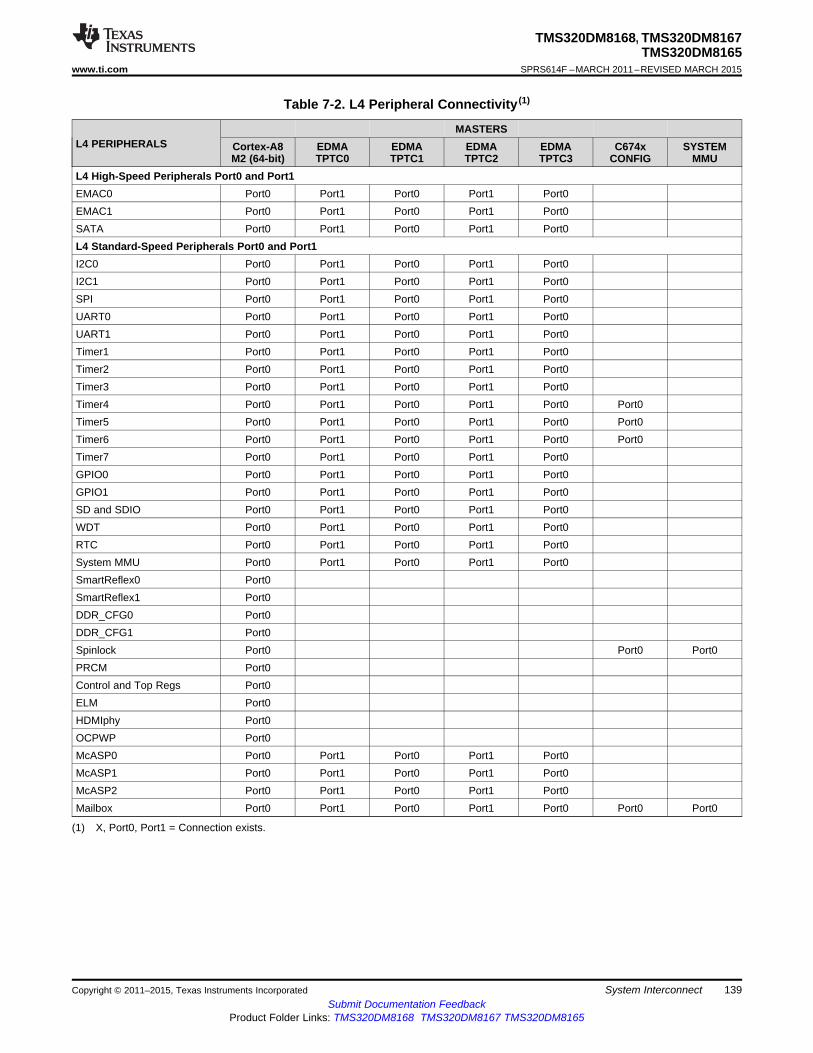
TMS320DM8168, TMS320DM8167TMS320DM8165
www.ti.com SPRS614F –MARCH 2011–REVISED MARCH 2015
Table 7-2. L4 Peripheral Connectivity (1)
MASTERSL4 PERIPHERALS Cortex-A8 EDMA EDMA EDMA EDMA C674x SYSTEM
M2 (64-bit) TPTC0 TPTC1 TPTC2 TPTC3 CONFIG MMUL4 High-Speed Peripherals Port0 and Port1EMAC0 Port0 Port1 Port0 Port1 Port0EMAC1 Port0 Port1 Port0 Port1 Port0SATA Port0 Port1 Port0 Port1 Port0L4 Standard-Speed Peripherals Port0 and Port1I2C0 Port0 Port1 Port0 Port1 Port0I2C1 Port0 Port1 Port0 Port1 Port0SPI Port0 Port1 Port0 Port1 Port0UART0 Port0 Port1 Port0 Port1 Port0UART1 Port0 Port1 Port0 Port1 Port0Timer1 Port0 Port1 Port0 Port1 Port0Timer2 Port0 Port1 Port0 Port1 Port0Timer3 Port0 Port1 Port0 Port1 Port0Timer4 Port0 Port1 Port0 Port1 Port0 Port0Timer5 Port0 Port1 Port0 Port1 Port0 Port0Timer6 Port0 Port1 Port0 Port1 Port0 Port0Timer7 Port0 Port1 Port0 Port1 Port0GPIO0 Port0 Port1 Port0 Port1 Port0GPIO1 Port0 Port1 Port0 Port1 Port0SD and SDIO Port0 Port1 Port0 Port1 Port0WDT Port0 Port1 Port0 Port1 Port0RTC Port0 Port1 Port0 Port1 Port0System MMU Port0 Port1 Port0 Port1 Port0SmartReflex0 Port0SmartReflex1 Port0DDR_CFG0 Port0DDR_CFG1 Port0Spinlock Port0 Port0 Port0PRCM Port0Control and Top Regs Port0ELM Port0HDMIphy Port0OCPWP Port0McASP0 Port0 Port1 Port0 Port1 Port0McASP1 Port0 Port1 Port0 Port1 Port0McASP2 Port0 Port1 Port0 Port1 Port0Mailbox Port0 Port1 Port0 Port1 Port0 Port0 Port0
(1) X, Port0, Port1 = Connection exists.
Copyright © 2011–2015, Texas Instruments Incorporated System Interconnect 139Submit Documentation Feedback
Product Folder Links: TMS320DM8168 TMS320DM8167 TMS320DM8165
TMS320DM8168, TMS320DM8167TMS320DM8165SPRS614F –MARCH 2011–REVISED MARCH 2015 www.ti.com
8 Power, Reset, Clocking, and Interrupts
8.1 Power Supplies
8.1.1 Voltage and Power DomainsThe device has the following voltage domains:• 1-V adaptive voltage scaling (AVS) domain - Main voltage domain for all modules• 1-V constant domain - Memories, PLLs, DACs, DDR IOs, HDMI, and USB PHYs• 1.8-V constant domain - PLLs, DACs, HDMI, and USB PHYs• 3.3-V constant domain - IOs and USB PHY• 1.5-V constant domain - DDR IOs, PCIe, and SATA SERDES• 0.9-V constant domain - USB PHY
These domains define groups of modules that share the same supply voltage for their core logic. Eachvoltage domain is powered by dedicated supply voltage rails. For the mapping between voltage domainsand the supply pins associated with each, see Table 4-33.
Note: A regulated supply voltage must be supplied to each voltage domain at all times, regardless of thepower domain states.
8.1.2 Power DomainsThe device's 1-V AVS and 1-V constant voltage domains have seven power domains that supply power toboth the core logic and SRAM within their associated modules. All other voltage domains have onlyalways-on power domain.
Within the 1-V AVS and 1-V constant voltage domains, each power domain, except for the always-ondomain, has an internal power switch that can completely remove power from that domain. At power-up,all domains, except always-on, come-up as power gated. Since there is an always-on domain in eachvoltage domain, all power supplies are expected to be ON all the time (as long as the device is in use).
For details on powering up or powering down the device power domains, see the TMS320DM816xDaVinci Digital Media Processors Technical Reference Manual (SPRUGX8).
Note: All modules within a power domain are unavailable when the domain is powered OFF. Forinstructions on powering ON or powering OFF the domains, see the TMS320DM816x DaVinci DigitalMedia Processors Technical Reference Manual (SPRUGX8).
8.1.3 1-V AVS and 1-V Constant Power Domains• HDVICP2-0 Domain
This power domain contains HDVICP2-0. If HDVICP2-0 is not used, it can be power gated.• HDVICP2-1 Domain
This power domain contains HDVICP2-1. If HDVICP2-1 is not used, it can be power gated.• HDVICP2-2 Domain
This power domain contains HDVICP2-2. If HDVICP2-2 is not used, it can be power gated.Note: Three HDVICP2 modules are available on the DM8168 and DM8167 devices and two HDVICP2modules (HDVICP2-0 and HDVICP2-1) are available on the DM8165 devices.
• Graphics DomainThis domain contains the SGX530 (available only on the DM8168 device).
• Active DomainThe active domain has all modules that are only needed when the system is in "active" state. In any ofthe standby states, these modules are not needed. This domain contains the C674x DSP andHDVPSS peripheral.
• Default Domain
140 Power, Reset, Clocking, and Interrupts Copyright © 2011–2015, Texas Instruments IncorporatedSubmit Documentation Feedback
Product Folder Links: TMS320DM8168 TMS320DM8167 TMS320DM8165
TMS320DM8168, TMS320DM8167TMS320DM8165
www.ti.com SPRS614F –MARCH 2011–REVISED MARCH 2015
The default domain contains modules that might be required even in standby mode. Having them in aseparate power domain allows customers to power gate these modules when in standby mode. Thisdomain has the DDR, SATA, PCIe, Media Controller and USB peripherals.
• Always-On DomainThe always-on domain contains all modules that are required even when the system goes to standbymode. This includes the host ARM and modules that generate wake-up interrupts (for example, UART,RTC, GPIO, EMAC) as well as other low-power IOs.
8.1.4 SmartReflex™The device contains SmartReflex modules that are required to minimize power consumption on thevoltage domains using external variable-voltage power supplies. Based on the device process,temperature, and desired performance, the SmartReflex modules advise the host processor to raise orlower the supply voltage to each domain for minimal power consumption. The communication link betweenthe host processor and the external regulators is a system-level decision and can be accomplished usingGPIOs or I2C.
The major technique employed by SmartReflex in the device is adaptive voltage scaling (AVS). Based onthe silicon process and temperature, the SmartReflex modules guide software in adjusting the core 1-Vsupply voltage within the desired range. This technique is called adaptive voltage scaling (AVS). AVSoccurs continuously and in real time, helping to minimize power consumption in response to changingoperating conditions.
NOTEImplementation of SmartReflex AVS is required for proper device operation.
8.1.5 Memory Power ManagementThe device memories offer three different modes to save power when memories are not being used;Table 8-1 provides the details.
Table 8-1. Memory Power Management Modes
MODE POWER SAVING WAKE-UP LATENCY MEMORY CONTENTSLight Sleep (LS) ~60% Low PreservedDeep Sleep (DS) ~75% Medium PreservedShut Down (SD) ~95% High Lost
The device provides a feature that allows the software to put the chip-level memories (C674x L2, OCMCRAMs) in any of the three (LS, DS, and SD) modes. There are control registers in the control module tocontrol the power-down state of C674x L2, OCMC RAM0, and OCMC RAM1. There are also statusregisters that can be used during power-up to check if memories are powered-up. For detailed instructionson entering and exiting from light sleep and deep sleep modes, see the TMS320DM816x DaVinci DigitalMedia Processors Technical Reference Manual (SPRUGX8).
Memories inside switchable domains go to the shut down (SD) state whenever the power domain goes tothe OFF state. Memories come back to functional state along with the domain power-up.
In order to reduce SRAM leakage, many SRAM blocks can be switched from active mode to shut-downmode. When SRAM is put in shut-down mode, the voltage supplied to it is automatically removed and alldata in that SRAM is lost.
All SRAM located in a switchable power domain (all domains except always-on) automatically enters shut-down mode whenever its assigned associated power domain goes to the OFF state. The SRAM returns tothe active state when the corresponding power domain returns to the ON state.
Copyright © 2011–2015, Texas Instruments Incorporated Power, Reset, Clocking, and Interrupts 141Submit Documentation Feedback
Product Folder Links: TMS320DM8168 TMS320DM8167 TMS320DM8165
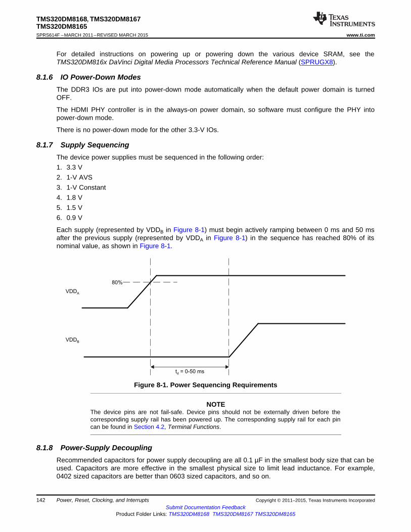
80%
t = 0-50 msd
VDDA
VDDB
TMS320DM8168, TMS320DM8167TMS320DM8165SPRS614F –MARCH 2011–REVISED MARCH 2015 www.ti.com
For detailed instructions on powering up or powering down the various device SRAM, see theTMS320DM816x DaVinci Digital Media Processors Technical Reference Manual (SPRUGX8).
8.1.6 IO Power-Down ModesThe DDR3 IOs are put into power-down mode automatically when the default power domain is turnedOFF.
The HDMI PHY controller is in the always-on power domain, so software must configure the PHY intopower-down mode.
There is no power-down mode for the other 3.3-V IOs.
8.1.7 Supply SequencingThe device power supplies must be sequenced in the following order:1. 3.3 V2. 1-V AVS3. 1-V Constant4. 1.8 V5. 1.5 V6. 0.9 V
Each supply (represented by VDDB in Figure 8-1) must begin actively ramping between 0 ms and 50 msafter the previous supply (represented by VDDA in Figure 8-1) in the sequence has reached 80% of itsnominal value, as shown in Figure 8-1.
Figure 8-1. Power Sequencing Requirements
NOTEThe device pins are not fail-safe. Device pins should not be externally driven before thecorresponding supply rail has been powered up. The corresponding supply rail for each pincan be found in Section 4.2, Terminal Functions.
8.1.8 Power-Supply DecouplingRecommended capacitors for power supply decoupling are all 0.1 µF in the smallest body size that can beused. Capacitors are more effective in the smallest physical size to limit lead inductance. For example,0402 sized capacitors are better than 0603 sized capacitors, and so on.
142 Power, Reset, Clocking, and Interrupts Copyright © 2011–2015, Texas Instruments IncorporatedSubmit Documentation Feedback
Product Folder Links: TMS320DM8168 TMS320DM8167 TMS320DM8165

TMS320DM8168, TMS320DM8167TMS320DM8165
www.ti.com SPRS614F –MARCH 2011–REVISED MARCH 2015
Table 8-2. Recommended Power-Supply DecouplingCapacitors
SUPPLY MINIMUM CAPACITOR NO.VDDA_PLL 2 (1)
DVDD1P8 2VDDT_SATA 2 (1)
VDDT_PCIE 3 (1)
CVDDC 20 (2)
DVDD_3p3 64 (2)
CVDD 28 (2)
(1) PLL supplies benefit from filters or ferrite beads to keep the noisefrom causing clock jitter. The minimum recommendation is a ferritebead with a resonance at 100 MHz along with at least one capacitoron the device side of the bead. Additional recommendation is to addone capacitor just before the bead to form a Pi filter. The filter needsto be as close as possible to the device pin, with the device-sidecapacitor being the most important component to be close to thedevice pin. PLL pins close together can be combined on the samesupply. PLL pins spaced farther away from one another may needindividual filtered supplies.
(2) It is recommended to have one bulk (15 µF or larger) capacitor forevery 10 smaller capacitors placed as closely as possible to thedevice.
DDR-related supply capacitor numbers are provided in Section 9.3.
8.2 Reset
8.2.1 System-Level Reset SourcesThe device has several types of system-level resets. Table 8-3 lists these reset types, along with the resetinitiator and the effects of each reset on the device.
Table 8-3. System-Level Reset Types
RESETS ALLMODULES, RESETS LATCHES BOOT ASSERTSTYPE INITIATOR EXCLUDING EMULATION PINS RSTOUT PIN
EMULATIONPower-On Reset (POR) POR pin Yes Yes Yes YesExternal Warm Reset RESET pin Yes No Yes YesEmulation Warm Reset On-Chip Emulation Yes No No Yes
LogicWatchdog Reset Watchdog Timer Yes No No YesSoftware Global Cold Reset Software Yes Yes No YesSoftware Global Warm Software Yes No No YesResetTest Reset TRST pin No Yes No No
8.2.2 Power-On Reset (POR pin)Power-on reset (POR) is initiated by the POR pin and is used to reset the entire chip, including the testand emulation logic. POR is also referred to as a cold reset since it is required to be asserted when thedevices goes through a power-up cycle. However, a device power-up cycle is not required to initiate apower-on reset.
The following sequence must be followed during a power-on reset:1. Wait for the power supplies to reach normal operating conditions while keeping the POR pin asserted.2. Wait for the input clock sources SERDES_CLKN and SERDES_CLKNP to be stable (if used by the
Copyright © 2011–2015, Texas Instruments Incorporated Power, Reset, Clocking, and Interrupts 143Submit Documentation Feedback
Product Folder Links: TMS320DM8168 TMS320DM8167 TMS320DM8165

TMS320DM8168, TMS320DM8167TMS320DM8165SPRS614F –MARCH 2011–REVISED MARCH 2015 www.ti.com
system) while keeping the POR pin asserted (low).3. Once the power supplies and the input clock source are stable, the POR pin must remain asserted
(low) for a minimum of 32 DEV_MXI cycles. Within the low period of the POR pin, the followinghappens:(a) All pins enter a Hi-Z mode.(b) The PRCM asserts reset to all modules within the device.(c) The PRCM begins propagating these clocks to the chip with the PLLs in bypass mode.
4. The POR pin may now be deasserted (driven high). When the POR pin is deasserted (high):(a) The BOOT pins are latched.(b) Reset to the ARM Cortex-A8 is de-asserted, provided the processor clock is running.(c) All other domain resets are released, provided the domain clocks are running.(d) The clock, reset, and power-down state of each peripheral is determined by the default settings of
the PRCM.(e) The ARM Cortex-A8 begins executing from the default address (Boot ROM).
8.2.3 External Warm Reset (RESET pin)An external warm reset is activated by driving the RESET pin active-low. This resets everything in thedevice, except the ARM Cortex-A8 interrupt controller, test, and emulation. An emulator session staysalive during warm reset.
The following sequence must be followed during a warm reset:1. Power supplies and input clock sources should already be stable.2. The RESET pin must be asserted (low) for a minimum of 32 DEV_MXI cycles. Within the low period of
the RESET pin, the following happens:(a) All pins, except test and emulation pins, enter a Hi-Z mode.(b) The PRCM asserts reset to all modules within the device, except for the ARM Cortex-A8 interrupt
controller, test, and emulation.(c) RSTOUT is asserted.
3. The RESET pin may now be de-asserted (driven high). When the RESET pin is de-asserted (high):(a) The BOOT pins are latched.(b) Reset to the ARM Cortex-A8 and modules without a local processor is de-asserted, with the
exception of the ARM Cortex-A8 interrupt controller, test, and emulation.(c) RSTOUT is de-asserted.(d) The clock, reset, and power-down state of each peripheral is determined by the default settings of
the PRCM.(e) The ARM Cortex-A8 begins executing from the default address (Boot ROM).(f) Since the ARM Cortex-A8 interrupt controller is not impacted by warm reset, application software
needs to explicitly clear all pending interrupts in the ARM Cortex-A8 interrupt controller.
8.2.4 Emulation Warm ResetAn emulation warm reset is activated by the on-chip emulation module. It has the same effect andrequirements as an external warm reset (RESET), with the exception that it does not re-latch the BOOTpins.
The emulator initiates an emulation warm reset via the ICEPick module. To invoke the emulation warmreset via the ICEPick module, the user can perform the following from the Code Composer Studio™ IDEmenu:
Debug → Advanced Resets → System Reset.
144 Power, Reset, Clocking, and Interrupts Copyright © 2011–2015, Texas Instruments IncorporatedSubmit Documentation Feedback
Product Folder Links: TMS320DM8168 TMS320DM8167 TMS320DM8165

TMS320DM8168, TMS320DM8167TMS320DM8165
www.ti.com SPRS614F –MARCH 2011–REVISED MARCH 2015
8.2.5 Watchdog ResetA watchdog reset is initiated when the watchdog timer counter reaches zero. It has the same effect andrequirements as an external warm reset (RESET), with the exception that it does not re-latch the BOOTpins. In addition, a watchdog reset always results in RSTOUT being asserted.
8.2.6 Software Global Cold ResetA software global cold reset is initiated under software control. It has the same effect and requirements asa power-on reset (POR), with the exception that it does not re-latch the BOOT pins.
Software initiates a software global cold reset by writing to RST_GLOBAL_COLD_SW in thePRM_RST_CTRL register.
8.2.7 Software Global Warm ResetA software global warm reset is initiated under software control. It has the same effect and requirementsas a external warm reset (RESET), with the exception that it does not re-latch the BOOT pins.
Software initiates a software global warm reset by writing to RST_GLOBAL_WARM_SW in thePRM_RST_CTRL register.
8.2.8 Test Reset (TRST pin)A test reset is activated by the emulator asserting the TRST pin. The only effect of a test reset is to resetthe emulation logic.
8.2.9 Local ResetThe local reset for various modules within the device is controlled by programming the PRCM and themodule's internal registers. Only the associated module is reset when a local reset is asserted, leaving therest of the device unaffected.
For details on local reset, see the PRCM chapter of the TMS320DM816x DaVinci Digital MediaProcessors Technical Reference Manual (SPRUGX8) and individual subsystem and peripheral user'sguides.
8.2.10 Reset PriorityIf any of the above reset sources occur simultaneously, the device only processes the highest-priorityreset request. The reset request priorities, from high to low, are as follows:1. Power-on reset (POR)2. Test reset (TRST)3. External warm reset (RESET)4. Emulation warm resets5. Watchdog reset6. Software global cold and warm resets.
8.2.11 Reset Status RegisterThe Reset Status Register (PRM_RSTST) contains information about the last reset that occurred in thesystem. For more information on this register, see the PRCM chapter of the TMS320DM816x DaVinciDigital Media Processors Technical Reference Manual (SPRUGX8).
8.2.12 PCIe Reset IsolationThe device supports reset isolation for the PCI Express (PCIe) module. This means that the PCI Expresssubsystem can be reset without resetting the rest of the device.
Copyright © 2011–2015, Texas Instruments Incorporated Power, Reset, Clocking, and Interrupts 145Submit Documentation Feedback
Product Folder Links: TMS320DM8168 TMS320DM8167 TMS320DM8165
TMS320DM8168, TMS320DM8167TMS320DM8165SPRS614F –MARCH 2011–REVISED MARCH 2015 www.ti.com
When the device is a PCI Express Root Complex (RC), the PCIe subsystem can be reset by softwarethrough the PRCM. Software should ensure that there are no ongoing PCIe transactions before assertingthis reset by first taking the PCIe subsystem into the IDLE state by programming the registerCM_DEFAULT_PCI_CLKCTRL inside the PRCM. After bringing the PCIe subsystem out of reset, busenumeration should be performed again and should treat all endpoints (EP) as if they had just beenconnected.
When the device is a PCI Express Endpoint (EP), the PCIe subsystem generates an interrupt when an in-band reset is received. Software should process this interrupt by putting the PCIe subsystem in the IDLEstate and then asserting the PCIe local reset through the PRCM.
All device-level resets mentioned in the previous sections, except Test Reset, also reset the PCIesubsystem. Therefore, the device should issue a Hot Reset to all downstream devices and re-enumeratethe bus upon coming out of reset.
8.2.13 RSTOUTThe RSTOUT pin on the device reflects device reset status and is de-asserted (high) when the device isout of reset. In addition, this output is always 3-stated and the internal pull resistor is disabled on this pinwhile POR or RESET is asserted; therefore, an external pullup or pulldown can be used to set the state ofthis pin (high or low) while POR or RESET is asserted. For more detailed information on external pullupsand pulldowns, see Section 6.3.1. This output is always asserted low when any of the following resetsoccur:• Power-on reset (POR)• External warm reset• Emulation warm reset (RESET)• Software global cold or warm reset• Watchdog timer reset.
The RSTOUT pin remains asserted until PRCM releases the host ARM Cortex-A8 processor for reset.
8.2.14 Effect of Reset on Emulation and TraceThe device emulation and trace is only reset by the following sources:• Power-on reset (POR)• Software global cold reset• Test reset (TRST).
Other than these three, none of the other resets affect emulation and trace functionality.
8.2.15 Reset During Power Domain SwitchingEach power domain has a dedicated warm reset and cold reset. Warm reset for a power domain isasserted under either of the following two conditions:1. A power-on reset, external warm reset, emulation warm reset, or software global cold or warm reset
occurs.2. When that power domain switches from the ON state to the OFF state.
Cold reset for a power domain is asserted under either of the following two conditions:1. A power-on reset or software global cold reset occurs.2. When that power domain switches from the ON state to the OFF state.
8.2.16 Pin Behaviors at ResetWhen any reset (other than test reset) described in Section 8.2.1 is asserted, all device pins are put into aHi-Z state except for:
146 Power, Reset, Clocking, and Interrupts Copyright © 2011–2015, Texas Instruments IncorporatedSubmit Documentation Feedback
Product Folder Links: TMS320DM8168 TMS320DM8167 TMS320DM8165
TMS320DM8168, TMS320DM8167TMS320DM8165
www.ti.com SPRS614F –MARCH 2011–REVISED MARCH 2015
• Emulation pins. These pins are only put into a Hi-Z state when POR or global software cold reset isasserted.
• RSTOUT pin.
In addition, the PINCNTL registers, which control pin multiplexing, slew control, enabling the pullup orpulldown, and enabling the receiver, are reset to the default state. For a description of the RESET_ISOregister, see the TMS320DM816x DaVinci Digital Media Processors Technical Reference Manual(SPRUGX8).
Internal pullup or pulldown (IPU or IPD) resistors are enabled during and immediately after reset asdescribed in the OTHER column in the tables in Section 4.2, Terminal Functions.
8.2.17 Reset Electrical Data and Timing
NOTEIf a configuration pin must be routed out from the device, the internal pullup or pulldown (IPUor IPD) resistor should not be relied upon; TI recommends the use of an external pullup orpulldown resistor.
Table 8-4. Timing Requirements for Reset(see Figure 8-2 and Figure 8-3)
NO. MIN MAX UNIT1 tw(RESET) Pulse duration, POR low or RESET low 32C (1) ns2 tsu(CONFIG) Setup time, boot and configuration pins valid before POR high or RESET 12C (1) ns
high (2)
3 th(CONFIG) Hold time, boot and configuration pins valid after POR high or RESET 0 nshigh (2)
(1) C = 1/DEV_MXI clock frequency, in ns. The device clock source must be stable and at a valid frequency prior to meeting the tw(RESET)requirement.
(2) For the list of boot and configuration pins, see Table 4-1, Boot Terminal Functions.
Table 8-5. Switching Characteristics Over Recommended Operating Conditions During Reset(see Figure 8-2)
NO. PARAMETER MIN MAX UNITtw(RSTL) Pulse width, RESET low 10C (1) ns
4 td(RSTL_IORST) Delay time, RESET falling to all IO entering reset state 0 14 ns5 td(RSTL_IOFUNC) Delay time, RESET rising to IO exiting reset state 0 14 ns
(1) C = 1/DEV_CLKIN clock frequency, in ns.
Copyright © 2011–2015, Texas Instruments Incorporated Power, Reset, Clocking, and Interrupts 147Submit Documentation Feedback
Product Folder Links: TMS320DM8168 TMS320DM8167 TMS320DM8165

DEV_CLKIN
POR
RESET
BTMODE[4:0]
Other I/O Pins(A)
Power Supplies Stable
1
2 3
5
ConfigHi-Z
4
54
RESET STATE
RESET STATE
DEV_CLKIN
POR
RESET
BTMODE[4:0]
Other I/O Pins(A)
PowerSuppliesRamping
Power Supplies Stable
Clock Source Stable
2 3
5
Config
5
Hi-Z
1
TMS320DM8168, TMS320DM8167TMS320DM8165SPRS614F –MARCH 2011–REVISED MARCH 2015 www.ti.com
A. For more detailed information on the reset state of each pin, see Section 8.2.16, Pin Behaviors at Reset. For the IPUand IPD settings during reset, see Section 4.2, Terminal Functions.
Figure 8-2. Power-Up Timing
A. For more detailed information on the reset state of each pin, see Section 8.2.16, Pin Behaviors at Reset. For the IPUand IPD settings during reset, see Section 4.2, Terminal Functions.
Figure 8-3. Warm Reset (RESET) Timing
8.3 ClockingThe device clocks are generated from several external reference clocks that are fed to on-chip PLLs anddividers (both inside and outside of the PRCM Module). Figure 8-4 shows a high-level overview of thedevice clocking structure. Note that to reduce complexity, all clocking connections are not shown. Fordetailed information on the device clocks, see the Device Clocking and Flying Adder PLL section of theTMS320DM816x DaVinci Digital Media Processors Technical Reference Manual (SPRUGX8).
148 Power, Reset, Clocking, and Interrupts Copyright © 2011–2015, Texas Instruments IncorporatedSubmit Documentation Feedback
Product Folder Links: TMS320DM8168 TMS320DM8167 TMS320DM8165

SE
RD
ES
27-MHzXTAL
Main
PLL
Clocks
OSC 27
Audio
PLL
Clocks
DDR
PLL
Clocks
audio reference clock
Video
PLL
Clocks
To DDR PHYsTo CEC, UART, and othersTo L3P, EMIF and DMM
DDR Clock4 (Spare)DDR Clock5 (Spare)
HD, SD, TMDS Clocks
Audio Clock1
Audio Clock2
Audio Clock3
To ARM Cortex-A8
To C674x DSP
To HDVICP2s
To L3, HDVPSS
To EMAC
To SGX530(A)
To USB
DEVCLKIN
PCIe SS
SATA SS
SE
RD
ES
100-MHzDifferential Clock
To RTC32.768-kHz
Clock
TMS320DM8168, TMS320DM8167TMS320DM8165
www.ti.com SPRS614F –MARCH 2011–REVISED MARCH 2015
A. SGX530 is available only on the DM8168 device.
Figure 8-4. System Clocking Overview
8.3.1 Device Clock InputsThe device has four on-chip PLLs and one reference clock which are generated by on-chip oscillators. Inaddition to the 27-MHz reference clock, a 100-MHz differential clock input is required for SATA and PCIe.A third clock input is an optional 32.768-kHz clock input (no on-chip oscillator) for the RTC.
The device clock input (DEV_MXI and DEV_CLKIN) is used to generate the majority of the internalreference clocks. An external square-wave clock can be supplied to DEV_CLKIN instead of using a crystalinput. The device clock should be 27 MHz.
Section 8.3.1.1 provides details on using the on-chip oscillators with external crystals for the 27-MHzsystem oscillator.
8.3.1.1 Using the Internal Oscillators
When the internal oscillators are used to generate the device clock, external crystals are required to beconnected across the MXI and MXO pins, along with two load capacitors, as shown in Figure 8-5. Theexternal crystal load capacitors should also be connected to the associated oscillator ground pin(DEVOSC_VSS). The capacitors should not be connected to board ground (VSS).
Copyright © 2011–2015, Texas Instruments Incorporated Power, Reset, Clocking, and Interrupts 149Submit Documentation Feedback
Product Folder Links: TMS320DM8168 TMS320DM8167 TMS320DM8165

)C(C
CC
21
21LC
+
=
DEV_MXI/DEV_CLKIN DEV_MXO
C1 C2
Crystal27 MHz
DEVOSC_VSS
1.8 V
DEVOSC_DVDD18 DEVOSC_VSS
R
(Optional)d
TMS320DM8168, TMS320DM8167TMS320DM8165SPRS614F –MARCH 2011–REVISED MARCH 2015 www.ti.com
Figure 8-5. 27-MHz System Oscillator
The load capacitors, C1 and C2 in Figure 8-5, should be chosen such that the equation below is satisfied.CL in the equation is the load specified by the crystal manufacturer. Rd is an optional damping resistor. Alldiscrete components used to implement the oscillator circuit should be placed as close as possible to theassociated oscillator MXI, MXO, and VSS pins.
Table 8-6. Input Requirements for Crystal Circuit on the Device OscillatorPARAMETER MIN NOM MAX UNIT
Start-up time (from power up until oscillating at stable frequency of 27 MHz) 4 msCrystal Oscillation frequency 27 MHzParallel Load Capacitance (C1 and C2) 12 24 pFCrystal ESR 60 OhmCrystal Shunt Capacitance 5 pFCrystal Oscillation Mode Fundamental OnlyCrystal Frequency stability ±50 ppm
150 Power, Reset, Clocking, and Interrupts Copyright © 2011–2015, Texas Instruments IncorporatedSubmit Documentation Feedback
Product Folder Links: TMS320DM8168 TMS320DM8167 TMS320DM8165

DEV_CLKIN
2
3
4
4
5 1
1
( )sM H z27
B W*
B W**2
10*10Α
20
-S N R
p=
TMS320DM8168, TMS320DM8167TMS320DM8165
www.ti.com SPRS614F –MARCH 2011–REVISED MARCH 2015
Table 8-7. DEV_CLKIN Clock Source Requirements (1) (2) (3)
(see Figure 8-6)NO. MIN NOM MAX UNIT
1 tc(DCK) Cycle time, DEV_CLKIN 37.037 ns2 tw(DCKH) Pulse duration, DEV_CLKIN high 0.45C 0.55C ns3 tw(DCKL) Pulse duration, DEV_CLKIN low 0.45C 0.55C ns4 tt(DCK) Transition time, DEV_CLKIN 7 ns5 tJ(DCK) Period jitter, DEV_CLKIN (VDACs not used) 150 ps
Period jitter, DEV_CLKIN (VDACs used) A sSf Frequency stability, DEV_CLKIN ±50 ppm
(1) The reference points for the rise and fall transitions are measured at VIL MAX and VIH MIN.(2) C = DEV_CLKIN cycle time in ns.(3)
Where SNR is the desired signal-to-noise ratio and BW is the highest DAC signal bandwidth used in the system (SD = 6 MHz, 720p or1080i = 30 MHz, 1080p = 60 MHz).
Figure 8-6. DEV_CLKIN Timing
8.3.2 SERDES_CLKN and SERDES_CLKP Input ClockA high-quality, low-jitter differential clock source is required for the PCIe and SATA PHYs. The clock isrequired to be AC coupled to the device's SERDES_CLKP and SERDES_CLKN pins according to thespecifications in Table 8-11. Both the clock source and the coupling capacitors should be placedphysically as close as possible to the processor.
When the PCIe interface is used, the SERDES_CLKN or SERDES_CLKP clock is required to meet theREFCLK AC specifications outlined in the PCI Express Card Electromechanical Specification (Gen.1 andGen.2). When the SATA interface is used, the SERDES_CLKN or SERDES_CLKP clock is required tomeet the specifications in Table 8-8. When both the PCIe and SATA interfaces are used, both sets ofspecifications must be met simultaneously.
Table 8-8. SERDES_CLKN and SERDES_CLKP Clock Source Requirements for SATAPARAMETER MIN TYP MAX UNIT
Clock Frequency 100 MHzJitter 50 Ps pk-pkDuty Cycle 40 60 %Rise and Fall Time 700 ps
An HCSL differential clock source is required to meet the REFCLK AC specifications outlined in the PCIExpress Card Electromechanical Specification, Rev. 2.0, at the input to the AC coupling capacitors. Inaddition, LVDS clock sources that are compliant to the above specification, but with the exceptions shownin Table 8-9, are also acceptable.
Copyright © 2011–2015, Texas Instruments Incorporated Power, Reset, Clocking, and Interrupts 151Submit Documentation Feedback
Product Folder Links: TMS320DM8168 TMS320DM8167 TMS320DM8165

TMS320DM8168, TMS320DM8167TMS320DM8165SPRS614F –MARCH 2011–REVISED MARCH 2015 www.ti.com
Table 8-9. Exceptions to REFCLK AC Specification for LVDS Clock SourcesSYMBOL PARAMETER MIN MAX UNIT
VIH Differential input high voltage (VIH) 125 1000 mVVIL Differential input high voltage (VIL) -1000 -125 mV
Table 8-10. SERDES_CLKN and SERDES_CLKP Routing SpecificationsPARAMETER MIN TYP MAX UNIT
Number of stubs allowed on SERDES_CLKN and SERDES_CLKP traces 0 StubsSERDES_CLKN and SERDES_CLKP trace length from oscillator to device 24000 (1) MilsSERDES_CLKN and SERDES_CLKP pair differential impedance 100 OhmsNumber of vias on each SERDES_CLKN and SERDES_CLKP trace (2) 3 ViasSERDES_CLKN and SERDES_CLKP differential pair to any other trace 2*DS (3)
spacing
(1) Keep trace length as short as possible.(2) Vias must be used in pairs with their distance minimized.(3) DS is the differential spacing of the SERDES_CLKN and SERDES_CLKP traces.
AC coupling capacitors are required on the SERDES_CLKN and SERDES_CLKP pair. Table 8-11 showsthe requirements for these capacitors.
Table 8-11. SERDES_CLKN and SERDES_CLKP AC Coupling Capacitors RequirementsPARAMETER MIN TYP MAX UNIT
SERDES_CLKN and SERDES_CLKP AC coupling capacitor value (1) 0.24 0.27 4 nFSERDES_CLKN and SERDES_CLKP AC coupling capacitor package 0402 10 Mils (2) (3)
size
(1) The value of this capacitor depends on several factors including differential input clock swing. For a 100-MHz differential clock with anapproximate 1-V voltage swing, the recommended typical value for the SERDES clock AC coupling capacitors is 270 pF. Deviating fromthis recommendation can result in the reduction of clock signal amplitude or lowering the noise rejection characteristics.
(2) LxW, 10 mil units; a 0402 is a 40x20 mil surface mount capacitor.(3) The physical size of the capacitor should be as small as possible.
8.3.3 CLKIN32 Input ClockAn external 32.768-kHz clock input can optionally be provided at the CLKIN32 pin to serve as a referenceclock in place of the RTCDIVIDER clock for the RTC and Timer modules. If the CLKIN32 pin is notconnected to a 32.768-kHz clock input, this pin should be pulled low. The CLKIN32 source must meet thetiming requirements shown in Table 8-12.
Table 8-12. Timing Requirements for CLKIN32 (1) (2)
(see Figure 8-7)NO. MIN NOM MAX UNIT
1 tc(CLKIN32) Cycle time, CLKIN32 1/32768 s2 tw(CLKIN32H) Pulse duration, CLKIN32 high 0.45C 0.55C ns3 tw(CKIN32L) Pulse duration, CLKIN32 low 0.45C 0.55C ns4 tt(CLKIN32) Transition time, CLKIN32 7 ns5 tJ(CLKIN32) Period jitter, CLKIN32 0.02C ns
(1) The reference points for the rise and fall transitions are measured at V IL MAX and V IH MIN.(2) C = CLKIN32 cycle time, in ns. For example, when CLKIN32 frequency is 32768 Hz, use C = 1/32768 s.
152 Power, Reset, Clocking, and Interrupts Copyright © 2011–2015, Texas Instruments IncorporatedSubmit Documentation Feedback
Product Folder Links: TMS320DM8168 TMS320DM8167 TMS320DM8165

( )( ) fr*
M*P*FREQ
Κ*Νfo ú
û
ùêë
é=
FREQFlying-AdderSynthesizer /M
/P PFD CP VCO
/N
fr
fs fo
K
fpfvco
CLKIN32
2
3
4
4
5 1
1
TMS320DM8168, TMS320DM8167TMS320DM8165
www.ti.com SPRS614F –MARCH 2011–REVISED MARCH 2015
Figure 8-7. CLKIN32 Timing
8.3.4 PLLsThe device contains four embedded PLLs (Main, Audio, Video and DDR) that provide clocks to differentparts of the system. For a high-level view of the device clock architecture, including the PLL referenceclock sources and connections, see Figure 8-4.
The reference clock for most of the PLLs comes from the DEV_CLKIN input clock. Also, each PLLsupports a bypass mode in which the reference clock can be directly passed to the PLL CLKOUT. Alldevice PLLs (except the DDR PLL) come-up in bypass mode after reset.
Flying-adder PLLs are used for all the on-chip PLLs. Figure 8-8 shows the basic structure of the flying-adder PLL.
Figure 8-8. Flying-Adder PLL
The flying-adder PLL has two main components: a multi-phase PLL and the flying-adder synthesizer. Themulti-phase PLL takes an input reference clock (fr), multiplies it with factor, N, and provides a K-phaseoutput to the flying-adder synthesizer. The flying-adder synthesizer takes this multi-phase clock input andproduces a variable frequency clock (fs). There can be a post divider on this clock which takes in clock fsand drives out clock fo. The frequency of the clock driven out is given by:
There can be multiple flying-adder synthesizers attached to one multi-phase PLL to generate differentfrequencies. In this case, FREQ (4 bits of integer and 24 bits of fractional value) and M (1 to 255) valuescan be adjusted for each clock separately, based on the frequency needed. The multi-phase PLL used inthis device has a value of K = 8.
For details on programming the device PLLs, see the PLL chapter of the TMS320DM816x DaVinci DigitalMedia Processors Technical Reference Manual (SPRUGX8).
Copyright © 2011–2015, Texas Instruments Incorporated Power, Reset, Clocking, and Interrupts 153Submit Documentation Feedback
Product Folder Links: TMS320DM8168 TMS320DM8167 TMS320DM8165

Η8
FREQ*M*A
N*8*PLL_CLKIN
10*P*FREQ)*Floor(M 6
--÷÷
ø
ö
çç
è
æ
TMS320DM8168, TMS320DM8167TMS320DM8165SPRS614F –MARCH 2011–REVISED MARCH 2015 www.ti.com
8.3.4.1 PLL Programming Limits
The PLL and Flying Adder Synthesizers support generation of a wide range of clocks that are allgenerated from the same input clock source. Therefore, these clocks are all synchronous. The flying-adder synthesizers take the multi-phase clock from the PLL and produce variable frequency clocks (fs) asstated in the previous section. Each variable frequency clock is then divided by a post divider before use.
The clock outputs from the PLL, Synthesizer and Post Divider contain period variations that must beconsidered. The minimum period of the generated clock is effectively the maximum clock rate. Differentconfigurations of the PLL dividers, Synthesizer and output dividers will have larger or smaller amounts ofphase variation. The equation below will calculate the minimum cycle period for a given set of settings.The result of the following minimum cycle equation must be greater than the value shown in Table 8-13.
The first term of the below equation is a characteristic of the Flying Adder PLL. The selection of M*FREQis important. Choosing a non-integer value of M*FREQ will cause larger period variation and a higher peakinstantaneous frequency. Use of non-integer M*FREQ can be done to create specific average frequenciesat the cost of higher phase variation. Using integer values of M*FREQ result in minimum phase variation.The second and third terms are PLL phase jitter terms associated with the frequency synthesis. Thesecond term is about 20ps and the third is normally 10ps.
Please refer to the Technical Reference Manual (SPRUGX8) for examples using this equation. The TRMalso contains a standard set of configurations that we recommend for customer use.
Where:
• PLL_CLKIN is the input clock frequency (in MHz) to the PLL before the P divider• Floor( ) = round down• M = PLL divider• FREQ = PLL frequency setting• A = 169 for all PLLs with the following exception: A = 218 for the audio PLL when its input is sourced
from the main PLL output• H = 0 if M * FREQ is a multiple of 8; otherwise, H = 10• 800 MHz ≤ PLL_CLKIN * N / P ≤ 1600 MHz• 10 MHz ≤ PLL_CLKIN / P ≤ 60 MHz
154 Power, Reset, Clocking, and Interrupts Copyright © 2011–2015, Texas Instruments IncorporatedSubmit Documentation Feedback
Product Folder Links: TMS320DM8168 TMS320DM8167 TMS320DM8165

TMS320DM8168, TMS320DM8167TMS320DM8165
www.ti.com SPRS614F –MARCH 2011–REVISED MARCH 2015
Table 8-13. PLL Clock Frequencies (1)
CLOCK DEVICE SPEED RANGE MIN CYCLE (ps)Main PLLClock 1 Blank 1250
2 10004 889
Clock 2 Blank 10002 8334 741
Clock 3 Blank 18762 16674 1481
Clock 4 Blank 20002 17864 1667
DDR PLLClock 2 Blank, 2, 4 18519Clock 3 Blank 2632
2 26324 2222
Video PLLClock 1 Blank, 2, 4 1515Clock 2 Blank, 2, 4 1515Clock 3 Blank, 2, 4 1515Audio PLLClock 2 Blank, 2, 4 6329Clock 3 Blank, 2, 4 5076Clock 4 Blank, 2, 4 5076Clock 5 Blank, 2, 4 5076
(1) For more information on the available device speed ranges for each part number, see Table 10-1
8.3.4.2 PLL Power Supply Filtering
The device PLLs are supplied externally via the VDDA_PLL power-supply pins. External filtering must beadded on the PLL supply pins to ensure that the requirements in Table 8-14 are met.
Table 8-14. Power Supply Requirements
PARAMETER MIN MAX UNITDynamic noise at VDDA_PLL pins 50 mV p-p
8.3.4.3 PLL Locking Sequence
All of the flying-adder PLLs (except the DDR PLL) come-up in bypass mode at reset. All of the registers(P, N, FREQ, and M) need to be programmed appropriately and then wait approximately 8 µs forPLL_Audio and 5 µs for the other PLLS to be locked. Verification that the PLL is locked can be checkedby accessing the lock status bit in the PLL control register for each PLL (bit = 1 when the PLL is locked).Once the PLL is locked, then the FA-PLL can be taken out of bypass mode. Control for bypass mode isthrough chip-level registers. For more details on the PLL registers and bypass logic, see the PLL chapterof the TMS320DM816x DaVinci Digital Media Processors Technical Reference Manual (SPRUGX8).
8.3.4.4 PLL Registers
The PLL control registers reside in the control module and are listed in Table 6-3.Copyright © 2011–2015, Texas Instruments Incorporated Power, Reset, Clocking, and Interrupts 155
Submit Documentation FeedbackProduct Folder Links: TMS320DM8168 TMS320DM8167 TMS320DM8165
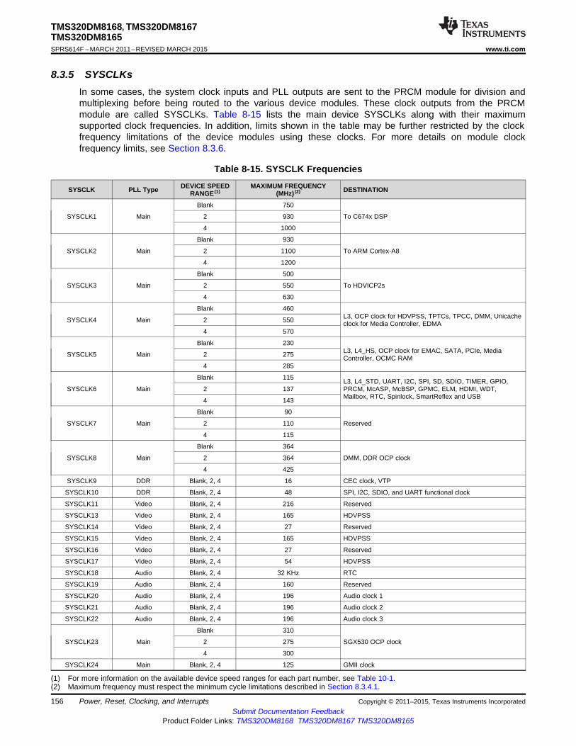
TMS320DM8168, TMS320DM8167TMS320DM8165SPRS614F –MARCH 2011–REVISED MARCH 2015 www.ti.com
8.3.5 SYSCLKsIn some cases, the system clock inputs and PLL outputs are sent to the PRCM module for division andmultiplexing before being routed to the various device modules. These clock outputs from the PRCMmodule are called SYSCLKs. Table 8-15 lists the main device SYSCLKs along with their maximumsupported clock frequencies. In addition, limits shown in the table may be further restricted by the clockfrequency limitations of the device modules using these clocks. For more details on module clockfrequency limits, see Section 8.3.6.
Table 8-15. SYSCLK FrequenciesDEVICE SPEED MAXIMUM FREQUENCYSYSCLK PLL Type DESTINATIONRANGE (1) (MHz) (2)
Blank 750
SYSCLK1 Main 2 930 To C674x DSP
4 1000
Blank 930
SYSCLK2 Main 2 1100 To ARM Cortex-A8
4 1200
Blank 500
SYSCLK3 Main 2 550 To HDVICP2s
4 630
Blank 460L3, OCP clock for HDVPSS, TPTCs, TPCC, DMM, UnicacheSYSCLK4 Main 2 550 clock for Media Controller, EDMA
4 570
Blank 230L3, L4_HS, OCP clock for EMAC, SATA, PCIe, MediaSYSCLK5 Main 2 275 Controller, OCMC RAM
4 285
Blank 115 L3, L4_STD, UART, I2C, SPI, SD, SDIO, TIMER, GPIO,SYSCLK6 Main 2 137 PRCM, McASP, McBSP, GPMC, ELM, HDMI, WDT,
Mailbox, RTC, Spinlock, SmartReflex and USB4 143
Blank 90
SYSCLK7 Main 2 110 Reserved
4 115
Blank 364
SYSCLK8 Main 2 364 DMM, DDR OCP clock
4 425
SYSCLK9 DDR Blank, 2, 4 16 CEC clock, VTP
SYSCLK10 DDR Blank, 2, 4 48 SPI, I2C, SDIO, and UART functional clock
SYSCLK11 Video Blank, 2, 4 216 Reserved
SYSCLK13 Video Blank, 2, 4 165 HDVPSS
SYSCLK14 Video Blank, 2, 4 27 Reserved
SYSCLK15 Video Blank, 2, 4 165 HDVPSS
SYSCLK16 Video Blank, 2, 4 27 Reserved
SYSCLK17 Video Blank, 2, 4 54 HDVPSS
SYSCLK18 Audio Blank, 2, 4 32 KHz RTC
SYSCLK19 Audio Blank, 2, 4 160 Reserved
SYSCLK20 Audio Blank, 2, 4 196 Audio clock 1
SYSCLK21 Audio Blank, 2, 4 196 Audio clock 2
SYSCLK22 Audio Blank, 2, 4 196 Audio clock 3
Blank 310
SYSCLK23 Main 2 275 SGX530 OCP clock
4 300
SYSCLK24 Main Blank, 2, 4 125 GMII clock
(1) For more information on the available device speed ranges for each part number, see Table 10-1.(2) Maximum frequency must respect the minimum cycle limitations described in Section 8.3.4.1.
156 Power, Reset, Clocking, and Interrupts Copyright © 2011–2015, Texas Instruments IncorporatedSubmit Documentation Feedback
Product Folder Links: TMS320DM8168 TMS320DM8167 TMS320DM8165
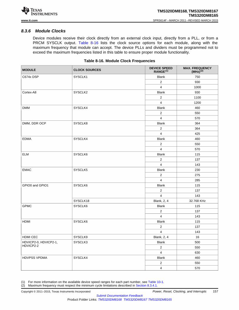
TMS320DM8168, TMS320DM8167TMS320DM8165
www.ti.com SPRS614F –MARCH 2011–REVISED MARCH 2015
8.3.6 Module ClocksDevice modules receive their clock directly from an external clock input, directly from a PLL, or from aPRCM SYSCLK output. Table 8-16 lists the clock source options for each module, along with themaximum frequency that module can accept. The device PLLs and dividers must be programmed not toexceed the maximum frequencies listed in this table to ensure proper module functionality.
Table 8-16. Module Clock Frequencies
DEVICE SPEED MAX. FREQUENCYMODULE CLOCK SOURCES RANGE (1) (MHz) (2)
C674x DSP SYSCLK1 Blank 7502 9304 1000
Cortex-A8 SYSCLK2 Blank 9302 11004 1200
DMM SYSCLK4 Blank 4602 5504 570
DMM, DDR OCP SYSCLK8 Blank 3642 3644 425
EDMA SYSCLK4 Blank 4602 5504 570
ELM SYSCLK6 Blank 1152 1374 143
EMAC SYSCLK5 Blank 2302 2754 285
GPIO0 and GPIO1 SYSCLK6 Blank 1152 1374 143
SYSCLK18 Blank, 2, 4 32.768 KHzGPMC SYSCLK6 Blank 115
2 1374 143
HDMI SYSCLK6 Blank 1152 1374 143
HDMI CEC SYSCLK9 Blank, 2, 4 16HDVICP2-0, HDVICP2-1, SYSCLK3 Blank 500HDVICP2-2 2 550
4 630HDVPSS VPDMA SYSCLK4 Blank 460
2 5504 570
(1) For more information on the available device speed ranges for each part number, see Table 10-1.(2) Maximum frequency must respect the minimum cycle limitations described in Section 8.3.4.1.
Copyright © 2011–2015, Texas Instruments Incorporated Power, Reset, Clocking, and Interrupts 157Submit Documentation Feedback
Product Folder Links: TMS320DM8168 TMS320DM8167 TMS320DM8165
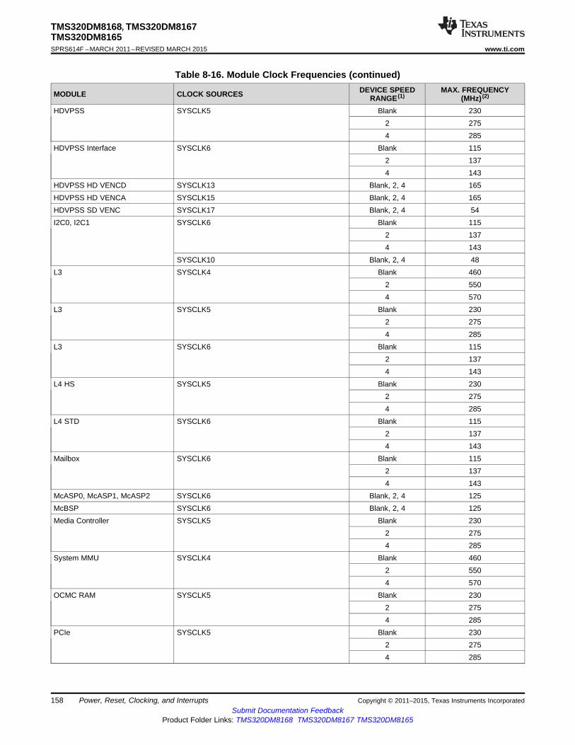
TMS320DM8168, TMS320DM8167TMS320DM8165SPRS614F –MARCH 2011–REVISED MARCH 2015 www.ti.com
Table 8-16. Module Clock Frequencies (continued)DEVICE SPEED MAX. FREQUENCYMODULE CLOCK SOURCES RANGE (1) (MHz) (2)
HDVPSS SYSCLK5 Blank 2302 2754 285
HDVPSS Interface SYSCLK6 Blank 1152 1374 143
HDVPSS HD VENCD SYSCLK13 Blank, 2, 4 165HDVPSS HD VENCA SYSCLK15 Blank, 2, 4 165HDVPSS SD VENC SYSCLK17 Blank, 2, 4 54I2C0, I2C1 SYSCLK6 Blank 115
2 1374 143
SYSCLK10 Blank, 2, 4 48L3 SYSCLK4 Blank 460
2 5504 570
L3 SYSCLK5 Blank 2302 2754 285
L3 SYSCLK6 Blank 1152 1374 143
L4 HS SYSCLK5 Blank 2302 2754 285
L4 STD SYSCLK6 Blank 1152 1374 143
Mailbox SYSCLK6 Blank 1152 1374 143
McASP0, McASP1, McASP2 SYSCLK6 Blank, 2, 4 125McBSP SYSCLK6 Blank, 2, 4 125Media Controller SYSCLK5 Blank 230
2 2754 285
System MMU SYSCLK4 Blank 4602 5504 570
OCMC RAM SYSCLK5 Blank 2302 2754 285
PCIe SYSCLK5 Blank 2302 2754 285
158 Power, Reset, Clocking, and Interrupts Copyright © 2011–2015, Texas Instruments IncorporatedSubmit Documentation Feedback
Product Folder Links: TMS320DM8168 TMS320DM8167 TMS320DM8165

TMS320DM8168, TMS320DM8167TMS320DM8165
www.ti.com SPRS614F –MARCH 2011–REVISED MARCH 2015
Table 8-16. Module Clock Frequencies (continued)DEVICE SPEED MAX. FREQUENCYMODULE CLOCK SOURCES RANGE (1) (MHz) (2)
RTC SYSCLK6 Blank 1152 1374 143
SYSCLK18 Blank, 2, 4 32.768 KHzSATA SYSCLK5 Blank 230
2 2754 285
SD, SDIO SYSCLK6 Blank 1152 1374 143
SYSCLK10 Blank, 2, 4 48SGX530 SYSCLK23 Blank 310
2 2754 300
SmartReflex SYSCLK6 Blank 1152 1374 143
SPI SYSCLK6 Blank 1152 1374 143
SYSCLK10 Blank, 2, 4 48Spinlock SYSCLK6 Blank 115
2 1374 143
Timers, WDT SYSCLK6 Blank 1152 1374 143
SYSCLK18 Blank, 2, 4 32.768 KHzUART0, UART1, UART2 SYSCLK6 Blank 115
2 1374 143
SYSCLK10 Blank, 2, 4 48USB0, USB1 SYSCLK6 Blank 115
2 1374 143
Copyright © 2011–2015, Texas Instruments Incorporated Power, Reset, Clocking, and Interrupts 159Submit Documentation Feedback
Product Folder Links: TMS320DM8168 TMS320DM8167 TMS320DM8165

CLKOUT(Divide-by-1)
241
3
4
Main PLL Clock5
DDR PLL Clock1
Video PLL Clock1
Audio PLL Clock1
CL
KO
UT
_M
UX
0
1
2
3
CLKOUT/n
(n=1...8)
TMS320DM8168, TMS320DM8167TMS320DM8165SPRS614F –MARCH 2011–REVISED MARCH 2015 www.ti.com
8.3.7 Output Clock Select LogicThe device includes one selectable general-purpose clock output (CLKOUT). The source for these outputclocks is controlled by the CLKOUT_MUX register in the control module and shown in Figure 8-9.
Figure 8-9. CLKOUT Source Selection Logic
As shown in the figure, there are four possible sources for CLKOUT, one clock from each of the fourPLLs. The selected clock can be further divided by any ratio from 1 to 1/8 before going out on theCLKOUT pin. The default selection is to select main PLL clock5, divider set to 1/1, and clock disabled.
Table 8-17. Switching Characteristics Over Recommended Operating Conditions for CLKOUT (1) (2)
(see Figure 8-10)NO PARAMETER MIN MAX UNIT.1 tc(CLKOUT) Cycle time, CLKOUT 10 ns2 tw(CLKOUTH) Pulse duration, CLKOUT high 0.45P 0.55P ns3 tw(CLKOUTL) Pulse duration, CLKOUT low 0.45P 0.55P ns4 tt(CLKOUT) Transition time, CLKOUT 0.05P ns
(1) The reference points for the rise and fall transitions are measured at VOL MAX and VOH MIN.(2) P = 1/CLKOUT clock frequency in nanoseconds (ns). For example, when CLKOUT frequency is 100 MHz, use P = 10 ns.
Figure 8-10. CLKOUT Timing
160 Power, Reset, Clocking, and Interrupts Copyright © 2011–2015, Texas Instruments IncorporatedSubmit Documentation Feedback
Product Folder Links: TMS320DM8168 TMS320DM8167 TMS320DM8165

TMS320DM8168, TMS320DM8167TMS320DM8165
www.ti.com SPRS614F –MARCH 2011–REVISED MARCH 2015
8.4 InterruptsThe device has a large number of interrupts. It also has masters (ARM Cortex™-A8, C674x DSP) capableof servicing interrupts. Specific details, such as the processing flow, configuration steps, and interruptcontroller registers, for each of these masters are found in their respective subsystem documentation.
8.4.1 Interrupt Summary ListTable 8-18 lists all the device interrupts by module and indicates the interrupt destination: ARM Cortex™-A8, C674x DSP.
Table 8-18. Interrupts By ModuleDESTINATION
MODULE INTERRUPT DESCRIPTIONCortex™-A8 C674x
POMBINTRREQ0Mailbox interrupt 0
POMBINTRPEND0 X
POMBINTRREQ1Mailbox interrupt 1
POMBINTRPEND1 X
POMBINTRREQ2HDVICP2-0 (1) Mailbox interrupt 2
POMBINTRPEND2
POSYNCINTRREQ0iCONT1 sync interrupt
POSYNCINTRPEND0 X X
POSYNCINTRREQ1iCONT2 sync interrupt
POSYNCINTRPEND1 X X
POMBINTRREQ0Mailbox interrupt 0
POMBINTRPEND0 X
POMBINTRREQ1Mailbox interrupt 1
POMBINTRPEND1 X
POMBINTRREQ2HDVICP2-1 (1) Mailbox interrupt 2
POMBINTRPEND2
POSYNCINTRREQ0iCONT1 sync interrupt
POSYNCINTRPEND0 X X
POSYNCINTRREQ1iCONT2 sync interrupt
POSYNCINTRPEND1 X X
POMBINTRREQ0Mailbox interrupt 0
POMBINTRPEND0 X
POMBINTRREQ1Mailbox interrupt 1
POMBINTRPEND1 X
POMBINTRREQ2HDVICP2-2 (1) Mailbox interrupt 2
POMBINTRPEND2
POSYNCINTRREQ0iCONT1 sync interrupt
POSYNCINTRPEND0 X X
POSYNCINTRREQ1iCONT2 sync interrupt
POSYNCINTRPEND1 X X
INTRQSerial ATA SATA Module interrupt
INTRQ_PEND_N X
(1) Three HDVICP2 modules are available on the DM8168 and DM8167 devices; two HDVICP2 modules (HDVICP2-0 and HDVICP2-1) areavailable on the DM8165 devices.
Copyright © 2011–2015, Texas Instruments Incorporated Power, Reset, Clocking, and Interrupts 161Submit Documentation Feedback
Product Folder Links: TMS320DM8168 TMS320DM8167 TMS320DM8165
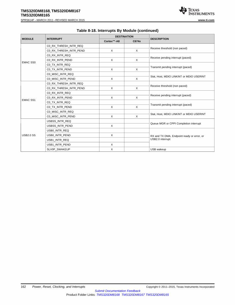
TMS320DM8168, TMS320DM8167TMS320DM8165SPRS614F –MARCH 2011–REVISED MARCH 2015 www.ti.com
Table 8-18. Interrupts By Module (continued)DESTINATION
MODULE INTERRUPT DESCRIPTIONCortex™-A8 C674x
C0_RX_THRESH_INTR_REQReceive threshold (non paced)
C0_RX_THRESH_INTR_PEND X X
C0_RX_INTR_REQReceive pending interrupt (paced)
C0_RX_INTR_PEND X XEMAC SS0
C0_TX_INTR_REQTransmit pending interrupt (paced)
C0_TX_INTR_PEND X X
C0_MISC_INTR_REQStat, Host, MDIO LINKINT or MDIO USERINT
C0_MISC_INTR_PEND X X
C0_RX_THRESH_INTR_REQReceive threshold (non paced)
C0_RX_THRESH_INTR_PEND X X
C0_RX_INTR_REQReceive pending interrupt (paced)
C0_RX_INTR_PEND X XEMAC SS1
C0_TX_INTR_REQTransmit pending interrupt (paced)
C0_TX_INTR_PEND X X
C0_MISC_INTR_REQStat, Host, MDIO LINKINT or MDIO USERINT
C0_MISC_INTR_PEND X X
USBSS_INTR_REQQueue MGR or CPPI Completion interrupt
USBSS_INTR_PEND X
USB0_INTR_REQ
USB2.0 SS USB0_INTR_PEND X RX and TX DMA, Endpoint ready or error, orUSB2.0 interruptUSB1_INTR_REQ
USB1_INTR_PEND X
SLV0P_SWAKEUP X USB wakeup
162 Power, Reset, Clocking, and Interrupts Copyright © 2011–2015, Texas Instruments IncorporatedSubmit Documentation Feedback
Product Folder Links: TMS320DM8168 TMS320DM8167 TMS320DM8165
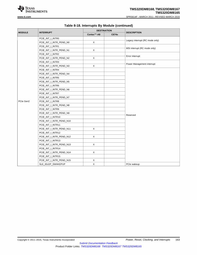
TMS320DM8168, TMS320DM8167TMS320DM8165
www.ti.com SPRS614F –MARCH 2011–REVISED MARCH 2015
Table 8-18. Interrupts By Module (continued)DESTINATION
MODULE INTERRUPT DESCRIPTIONCortex™-A8 C674x
PCIE_INT_I_INTR0Legacy interrupt (RC mode only)
PCIE_INT_I_INTR_PEND_N0 X
PCIE_INT_I_INTR1MSI interrupt (RC mode only)
PCIE_INT_I_INTR_PEND_N1 X
PCIE_INT_I_INTR2Error interrupt
PCIE_INT_I_INTR_PEND_N2 X
PCIE_INT_I_INTR3Power Management interrupt
PCIE_INT_I_INTR_PEND_N3 X
PCIE_INT_I_INTR4
PCIE_INT_I_INTR_PEND_N4
PCIE_INT_I_INTR5
PCIE_INT_I_INTR_PEND_N5
PCIE_INT_I_INTR6
PCIE_INT_I_INTR_PEND_N6
PCIE_INT_I_INTR7
PCIE_INT_I_INTR_PEND_N7
PCIe Gen2 PCIE_INT_I_INTR8
PCIE_INT_I_INTR_PEND_N8
PCIE_INT_I_INTR9
PCIE_INT_I_INTR_PEND_N9Reserved
PCIE_INT_I_INTR10
PCIE_INT_I_INTR_PEND_N10
PCIE_INT_I_INTR11
PCIE_INT_I_INTR_PEND_N11 X
PCIE_INT_I_INTR12
PCIE_INT_I_INTR_PEND_N12 X
PCIE_INT_I_INTR13
PCIE_INT_I_INTR_PEND_N13 X
PCIE_INT_I_INTR14
PCIE_INT_I_INTR_PEND_N14 X
PCIE_INT_I_INTR15
PCIE_INT_I_INTR_PEND_N15 X
SLE_IDLEP_SWAKEPUP X PCIe wakeup
Copyright © 2011–2015, Texas Instruments Incorporated Power, Reset, Clocking, and Interrupts 163Submit Documentation Feedback
Product Folder Links: TMS320DM8168 TMS320DM8167 TMS320DM8165

TMS320DM8168, TMS320DM8167TMS320DM8165SPRS614F –MARCH 2011–REVISED MARCH 2015 www.ti.com
Table 8-18. Interrupts By Module (continued)DESTINATION
MODULE INTERRUPT DESCRIPTIONCortex™-A8 C674x
TPCC_INT_PO[0]Region 0 DMA completion
TPCC_INT_PEND_N[0] X
TPCC_INT_PO[1]Region 1 DMA completion
TPCC_INT_PEND_N[1] X
TPCC_INT_PO[2]Region 2 DMA completion
TPCC_INT_PEND_N[2]
TPCC_INT_PO[3]Region 3 DMA completion
TPCC_INT_PEND_N[3]
TPCC_INT_PO[4]Region 4 DMA completion
TPCC_INT_PEND_N[4]
TPCC_INT_PO[5]TPCC Region 5 DMA completion
TPCC_INT_PEND_N[5]
TPCC_INT_PO[6]Region 6 DMA completion
TPCC_INT_PEND_N[6]
TPCC_INT_PO[7]Region 7 DMA completion
TPCC_INT_PEND_N[7]
TPCC_MPINT_POMemory protection error
TPCC_MPINT_PEND_N X
TPCC_ERRINT_POTPCC error
TPCC_ERRINT_PEND_N X X
TPCC_INTG_PODMA Global completion
TPCC_INTG_PEND_N
TPTC_ERRINT_POTPTC0 error
TPTC_LERRINT_PO X XTPTC 0
TPTC_INT_POTPTC0 completion
TPTC_LINT_PO
TPTC_ERRINT_POTPTC1 error
TPTC_LERRINT_PO XTPTC 1
TPTC_INT_POTPTC1 completion
TPTC_LINT_PO
TPTC_ERRINT_POTPTC2 error
TPTC_LERRINT_PO XTPTC 2
TPTC_INT_POTPTC2 completion
TPTC_LINT_PO
TPTC_ERRINT_POTPTC3 error
TPTC_LERRINT_PO XTPTC 3
TPTC_INT_POTPTC3 completion
TPTC_LINT_PO
SYS_ERR_INTRDDR EMIF4d 0
SYS_ERR_INTR_PEND_N XEMIF error
SYS_ERR_INTRDDR EMIF4d 1
SYS_ERR_INTR_PEND_N X
GPMC GPMC_SINTERRUPT X GPMC interrupt
UART 0 NIRQ X X UART and IrDA 0 interrupt
UART 1 NIRQ X X UART and IrDA 1 interrupt
UART 2 NIRQ X X UART and IrDA 2 interrupt
POINTR_REQTimer1 32-bit Timer1 interrupt
POINTR_PEND X X
POINTR_REQTimer2 32-bit Timer2 interrupt
POINTR_PEND X X
164 Power, Reset, Clocking, and Interrupts Copyright © 2011–2015, Texas Instruments IncorporatedSubmit Documentation Feedback
Product Folder Links: TMS320DM8168 TMS320DM8167 TMS320DM8165

TMS320DM8168, TMS320DM8167TMS320DM8165
www.ti.com SPRS614F –MARCH 2011–REVISED MARCH 2015
Table 8-18. Interrupts By Module (continued)DESTINATION
MODULE INTERRUPT DESCRIPTIONCortex™-A8 C674x
POINTR_REQTimer3 32-bit Timer3 interrupt
POINTR_PEND X X
POINTR_REQTimer4 32-bit Timer4 interrupt
POINTR_PEND X X
POINTR_REQTimer5 32-bit Timer5 interrupt
POINTR_PEND X X
POINTR_REQTimer6 32-bit Timer6 interrupt
POINTR_PEND X X
POINTR_REQTimer7 32-bit Timer7 interrupt
POINTR_PEND X X
WDTimer1 PO_INT_REQ X X Watchdog Timer
POINTRREQI2C0
POINTRPEND X XI2C Bus interrupt
POINTRREQI2C1
POINTRPEND X X
SPI SINTERRUPTN X X SPI Interrupt
SDIO IRQOQN X X SDIO interrupt
MCASP_X_INTR_REQMcASP 0 Transmit interrupt
MCASP_X_INTR_PEND X XMcASP 0
MCASP_R_INTR_REQMcASP 0 Receive interrupt
MCASP_R_INTR_PEND X X
MCASP_X_INTR_REQMcASP 1 Transmit interrupt
MCASP_X_INTR_PEND X XMcASP 1
MCASP_R_INTR_REQMcASP 1 Receive interrupt
MCASP_R_INTR_PEND X X
MCASP_X_INTR_REQMcASP 2 Transmit interrupt
MCASP_X_INTR_PEND X XMcASP 2
MCASP_R_INTR_REQMcASP 2 Receive interrupt
MCASP_R_INTR_PEND X X
PORRINTERRUPT McBSP Receive Int (legacy mode)
PORXINTERRUPT McBSP Transmit Int (legacy mode)McBSP
PORROVFLINTERRUPT McBSP Receive Overflow Int (legacy mode)
PORCOMMONIRQ X X McBSP Common Int
TIMER_INTR_REQTimer interrupt
TIMER_INTR_PEND XRTC
ALARM_INTR_REQAlarm interrupt
ALARM_INTR_PEND X
POINTRREQ1GPIO 0 interrupt 1
POINTRPEND1 X XGPIO 0
POINTRREQ2GPIO 0 interrupt 2
POINTRPEND2 X X
POINTRREQ1GPIO 1 interrupt 1
POINTRPEND1 X XGPIO 1
POINTRREQ2GPIO 1 interrupt 2
POINTRPEND2 X X
PRCM Reserved
Copyright © 2011–2015, Texas Instruments Incorporated Power, Reset, Clocking, and Interrupts 165Submit Documentation Feedback
Product Folder Links: TMS320DM8168 TMS320DM8167 TMS320DM8165

TMS320DM8168, TMS320DM8167TMS320DM8165SPRS614F –MARCH 2011–REVISED MARCH 2015 www.ti.com
Table 8-18. Interrupts By Module (continued)DESTINATION
MODULE INTERRUPT DESCRIPTIONCortex™-A8 C674x
INTR0_INTR Intr0 pulse version
INTR0_INTR_PEND_N X Intr0 level version
INTR1_INTR Intr1 pulse version
INTR1_INTR_PEND_N X Intr1 level versionHDVPSS
INTR2_INTR Intr2 pulse version
INTR2_INTR_PEND_N Intr2 level version
INTR3_INTR Intr3 pulse version
INTR3_INTR_PEND_N Intr3 level version
THALIAIRQ X Error in the IMG busSGX530 TARGETSINTERRUPT Target slave error interrupt(DM8168 only)
INITMINTERRUPT Initiator master error interrupt
INTR0_INTR Intr0 pulse versionHDMI 1.3Transmit INTR0_INTR_PEND_N X X Intr0 level version
INTRREQ SVT SmartReflex interrupt pulse versionSmartReflex0
INTRPEND X SVT SmartReflex interrupt level version
INTRREQ HVT SmartReflex interrupt pulse versionSmartReflex1
INTRPEND X HVT SmartReflex interrupt level version
PBIST Reserved
MAIL_U0_IRQ X
MAIL_U1_IRQ XMailbox Mailbox interrupt
MAIL_U2_IRQ
MAIL_U3_IRQ
NMI NMI_INT X NMI Interrupt
L3_DBG_IRQ X L3 debug errorInfrastructure
L3_APP_IRQ X L3 application error
System MMU MMU_INTR X Table walk abort
DMM DMM_HIGH_INTRPEND X PAT fault
COMMTX XARM ICECrusher interrupt
COMMRX X
Cortex™-A8 SS BENCH X ARM NPMUIRQ
ELM_IRQ X Error Location process completion
EMUINT X E2ICE interrupt
EVT0 X
EVT1 XC674x EVT2 X(Int Ctrl)
EVT3 X
INTERR X
C674x (ECM) EMU_DTDMA X
EMU_RTDXRX XC674x (RTDX)
EMU_RTDXTX X
IDMAINT0 XC674x Internal
C674x (EMC) IDMAINT1 X
EMC_IDMAERR X
C674x (PBIST) PBISTINT X
C674x (EFI A) EFIINTA X
C674x (EFI B) EFIINTB X
C674x (PMC) PMC_ED X
UMC_ED1 XC674x (UMC)
UMC_ED2 X
C674x (PDC) PDC_INT X
166 Power, Reset, Clocking, and Interrupts Copyright © 2011–2015, Texas Instruments IncorporatedSubmit Documentation Feedback
Product Folder Links: TMS320DM8168 TMS320DM8167 TMS320DM8165

TMS320DM8168, TMS320DM8167TMS320DM8165
www.ti.com SPRS614F –MARCH 2011–REVISED MARCH 2015
Table 8-18. Interrupts By Module (continued)DESTINATION
MODULE INTERRUPT DESCRIPTIONCortex™-A8 C674x
SYS SYS_CMPA X Sys
PMC_CMPA XC674x (PMC)
PMC_DMPA X
DMC_CMPA XC674x (DMC)
DMC_DMPA XC674x Internal
UMC_CMPA XC674x (UMC)
UMC_DMPA X
EMC_CMPA XC674x (EMC)
EMC_BUSERR X
Copyright © 2011–2015, Texas Instruments Incorporated Power, Reset, Clocking, and Interrupts 167Submit Documentation Feedback
Product Folder Links: TMS320DM8168 TMS320DM8167 TMS320DM8165
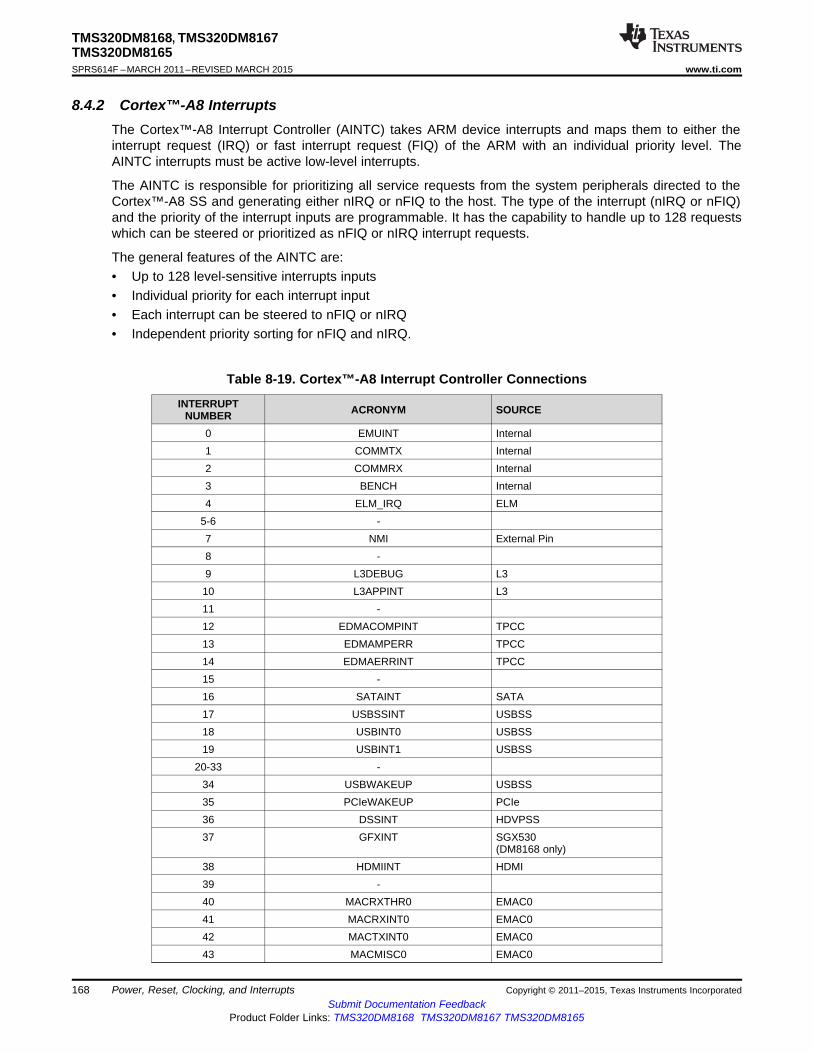
TMS320DM8168, TMS320DM8167TMS320DM8165SPRS614F –MARCH 2011–REVISED MARCH 2015 www.ti.com
8.4.2 Cortex™-A8 InterruptsThe Cortex™-A8 Interrupt Controller (AINTC) takes ARM device interrupts and maps them to either theinterrupt request (IRQ) or fast interrupt request (FIQ) of the ARM with an individual priority level. TheAINTC interrupts must be active low-level interrupts.
The AINTC is responsible for prioritizing all service requests from the system peripherals directed to theCortex™-A8 SS and generating either nIRQ or nFIQ to the host. The type of the interrupt (nIRQ or nFIQ)and the priority of the interrupt inputs are programmable. It has the capability to handle up to 128 requestswhich can be steered or prioritized as nFIQ or nIRQ interrupt requests.
The general features of the AINTC are:• Up to 128 level-sensitive interrupts inputs• Individual priority for each interrupt input• Each interrupt can be steered to nFIQ or nIRQ• Independent priority sorting for nFIQ and nIRQ.
Table 8-19. Cortex™-A8 Interrupt Controller Connections
INTERRUPT ACRONYM SOURCENUMBER0 EMUINT Internal1 COMMTX Internal2 COMMRX Internal3 BENCH Internal4 ELM_IRQ ELM
5-6 -7 NMI External Pin8 -9 L3DEBUG L310 L3APPINT L311 -12 EDMACOMPINT TPCC13 EDMAMPERR TPCC14 EDMAERRINT TPCC15 -16 SATAINT SATA17 USBSSINT USBSS18 USBINT0 USBSS19 USBINT1 USBSS
20-33 -34 USBWAKEUP USBSS35 PCIeWAKEUP PCIe36 DSSINT HDVPSS37 GFXINT SGX530
(DM8168 only)38 HDMIINT HDMI39 -40 MACRXTHR0 EMAC041 MACRXINT0 EMAC042 MACTXINT0 EMAC043 MACMISC0 EMAC0
168 Power, Reset, Clocking, and Interrupts Copyright © 2011–2015, Texas Instruments IncorporatedSubmit Documentation Feedback
Product Folder Links: TMS320DM8168 TMS320DM8167 TMS320DM8165

TMS320DM8168, TMS320DM8167TMS320DM8165
www.ti.com SPRS614F –MARCH 2011–REVISED MARCH 2015
Table 8-19. Cortex™-A8 Interrupt Controller Connections (continued)INTERRUPT ACRONYM SOURCENUMBER
44 MACRXTHR1 EMAC145 MACRXINT1 EMAC146 MACTXINT1 EMAC147 MACMISC1 EMAC148 PCIINT0 PCIe49 PCIINT1 PCIe50 PCIINT2 PCIe51 PCIINT3 PCIe
52-63 -64 SDINT SD, SDIO65 SPIINT SPI66 -67 TINT1 Timer168 TINT2 Timer269 TINT3 Timer370 I2CINT0 I2C071 I2CINT1 I2C172 UARTINT0 UART073 UARTINT1 UART174 UARTINT2 UART275 RTCINT RTC76 RTCALARMINT RTC77 MBINT Mailbox
78-79 -80 MCATXINT0 McASP081 MCARXINT0 McASP082 MCATXINT1 McASP183 MCARXINT1 McASP184 MCATXINT2 McASP285 MCARXINT2 McASP286 MCBSPINT McBSP
87-90 -91 WDTINT WDTIMER192 TINT4 Timer493 TINT5 Timer594 TINT6 Timer695 TINT7 Timer796 GPIOINT0A GPIO 097 GPIOINT0B GPIO 098 GPIOINT1A GPIO 199 GPIOINT1B GPIO 1
100 GPMCINT GPMC101 DDRERR0 DDR EMIF0102 DDRERR1 DDR EMIF1103 HDVICP0CONT1SYNC HDVICP2-0104 HDVICP0CONT2SYNC HDVICP2-0105 HDVICP1CONT1SYNC HDVICP2-1
Copyright © 2011–2015, Texas Instruments Incorporated Power, Reset, Clocking, and Interrupts 169Submit Documentation Feedback
Product Folder Links: TMS320DM8168 TMS320DM8167 TMS320DM8165
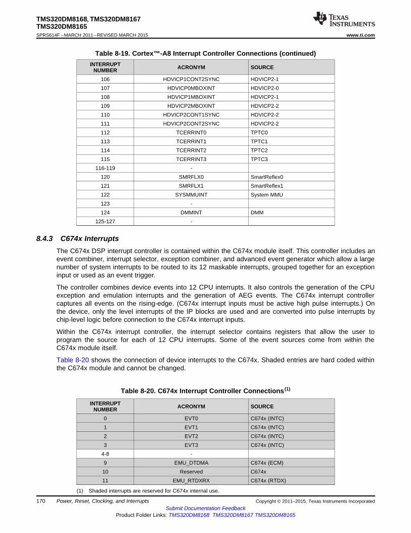
TMS320DM8168, TMS320DM8167TMS320DM8165SPRS614F –MARCH 2011–REVISED MARCH 2015 www.ti.com
Table 8-19. Cortex™-A8 Interrupt Controller Connections (continued)INTERRUPT ACRONYM SOURCENUMBER
106 HDVICP1CONT2SYNC HDVICP2-1107 HDVICP0MBOXINT HDVICP2-0108 HDVICP1MBOXINT HDVICP2-1109 HDVICP2MBOXINT HDVICP2-2110 HDVICP2CONT1SYNC HDVICP2-2111 HDVICP2CONT2SYNC HDVICP2-2112 TCERRINT0 TPTC0113 TCERRINT1 TPTC1114 TCERRINT2 TPTC2115 TCERRINT3 TPTC3
116-119 -120 SMRFLX0 SmartReflex0121 SMRFLX1 SmartReflex1122 SYSMMUINT System MMU123 -124 DMMINT DMM
125-127 -
8.4.3 C674x InterruptsThe C674x DSP interrupt controller is contained within the C674x module itself. This controller includes anevent combiner, interrupt selector, exception combiner, and advanced event generator which allow a largenumber of system interrupts to be routed to its 12 maskable interrupts, grouped together for an exceptioninput or used as an event trigger.
The controller combines device events into 12 CPU interrupts. It also controls the generation of the CPUexception and emulation interrupts and the generation of AEG events. The C674x interrupt controllercaptures all events on the rising-edge. (C674x interrupt inputs must be active high pulse interrupts.) Onthe device, only the level interrupts of the IP blocks are used and are converted into pulse interrupts bychip-level logic before connection to the C674x interrupt inputs.
Within the C674x interrupt controller, the interrupt selector contains registers that allow the user toprogram the source for each of 12 CPU interrupts. Some of the event sources come from within theC674x module itself.
Table 8-20 shows the connection of device interrupts to the C674x. Shaded entries are hard coded withinthe C674x module and cannot be changed.
Table 8-20. C674x Interrupt Controller Connections (1)
INTERRUPT ACRONYM SOURCENUMBER0 EVT0 C674x (INTC)1 EVT1 C674x (INTC)2 EVT2 C674x (INTC)3 EVT3 C674x (INTC)
4-8 -9 EMU_DTDMA C674x (ECM)10 Reserved C674x11 EMU_RTDXRX C674x (RTDX)
(1) Shaded interrupts are reserved for C674x internal use.
170 Power, Reset, Clocking, and Interrupts Copyright © 2011–2015, Texas Instruments IncorporatedSubmit Documentation Feedback
Product Folder Links: TMS320DM8168 TMS320DM8167 TMS320DM8165

TMS320DM8168, TMS320DM8167TMS320DM8165
www.ti.com SPRS614F –MARCH 2011–REVISED MARCH 2015
Table 8-20. C674x Interrupt Controller Connections(1) (continued)INTERRUPT ACRONYM SOURCENUMBER
12 EMU_RTDXTX C674x (RTDX)13 IDMAINT0 C674x (EMC)14 IDMAINT1 C674x (EMC)15 SDINT SD, SDIO16 SPIINT SPI
17-19 -20 EDMAINT TPCC21 EDMAERRINT TPCC22 TCERRINT0 TPTC0
23-31 -32 MACRXTHR0 EMAC033 MACRXINT0 EMAC034 MACTXINT0 EMAC035 MACMISC0 EMAC036 MACRXTHR1 EMAC137 MACRXINT1 EMAC138 MACTXINT1 EMAC139 MACMISC1 EMAC140 DSSINT HDVPSS41 HDMIINT HDMI
42-46 -47 WDTINT WDTIMER148 -49 TINT1 Timer150 TINT2 Timer251 TINT3 Timer352 TINT4 Timer453 TINT5 Timer554 TINT6 Timer655 TINT7 Timer756 MBINT Mailbox57 -58 I2CINT0 I2C059 I2CINT1 I2C160 UARTINT0 UART061 UARTINT1 UART162 UARTINT2 UART263 -64 GPIOINT0A GPIO 065 GPIOINT0B GPIO 066 GPIOINT1A GPIO 167 GPIOINT1B GPIO 1
68-69 -70 MCATXINT0 McASP071 MCARXINT0 McASP072 MCATXINT1 McASP173 MCARXINT1 McASP1
Copyright © 2011–2015, Texas Instruments Incorporated Power, Reset, Clocking, and Interrupts 171Submit Documentation Feedback
Product Folder Links: TMS320DM8168 TMS320DM8167 TMS320DM8165

TMS320DM8168, TMS320DM8167TMS320DM8165SPRS614F –MARCH 2011–REVISED MARCH 2015 www.ti.com
Table 8-20. C674x Interrupt Controller Connections(1) (continued)INTERRUPT ACRONYM SOURCENUMBER
74 MCATXINT2 McASP275 MCARXINT2 McASP276 MCBSPINT McBSP
77-86 -87 HDVICP2CONT1SYNC HDVICP2-288 HDVICP2CONT2SYNC HDVICP2-289 HDVICP2MBOXINT HDVICP2-290 HDVICP0CONT1SYNC HDVICP2-091 HDVICP0CONT2SYNC HDVICP2-092 HDVICP1CONT1SYNC HDVICP2-193 HDVICP1CONT2SYNC HDVICP2-194 HDVICP0MBOXINT HDVICP2-095 HDVICP1MBOXINT HDVICP2-196 INTERR C674x (INTC)97 EMC_IDMAERR C674x (EMC)98 PBISTINT C674x (PBIST)99 Reserved C674x
100 EFIINTA C674x (EFI A)101 EFIINTB C674x (EFI B)
102-112 Reserved C674x113 PMC_ED C674x (PMC)
114-115 Reserved C674x116 UMC_ED1 C674x (UMC)117 UMC_ED2 C674x (UMC)118 PDC_INT C674x (PDC)119 SYS_CMPA SYS120 PMC_CMPA C674x (PMC)121 PMC_DMPA C674x (PMC)122 DMC_CMPA C674x (DMC)123 DMC_DMPA C674x (DMC)124 UMC_CMPA C674x (UMC)125 UMC_DMPA C674x (UMC)126 EMC_CMPA C674x (EMC)127 EMC_BUSERR C674x (EMC)
172 Power, Reset, Clocking, and Interrupts Copyright © 2011–2015, Texas Instruments IncorporatedSubmit Documentation Feedback
Product Folder Links: TMS320DM8168 TMS320DM8167 TMS320DM8165

V = V MAX (or V MAX)ref IL OL
V = V MIN (or V MIN)ref IH OH
Vref
Transmission Line
4.0 pF 1.85 pF
Z0 = 50(see Note)
Ω
Tester Pin Electronics Data Sheet Timing Reference Point
OutputUnderTest
NOTE: The data sheet provides timing at the device pin. For output timing analysis, the tester pin electronics and its transmission line effects must betaken into account.A transmission line with a delay of 2 ns can be used to produce the desired transmission line effect. The transmission line isintended as a load only. It is not necessary to add or subtract the transmission line delay (2 ns) from the data sheet timings.
Input requirements in this data sheet are tested with an input slew rate of < 4 Volts per nanosecond (4 V/ns) at the device pin.
42 Ω 3.5 nH
Device Pin(see Note)
TMS320DM8168, TMS320DM8167TMS320DM8165
www.ti.com SPRS614F –MARCH 2011–REVISED MARCH 2015
9 Peripheral Information and Timings
9.1 Parameter Information
Figure 9-1. Test Load Circuit for AC Timing Measurements
The load capacitance value stated is only for characterization and measurement of AC timing signals. Thisload capacitance value does not indicate the maximum load the device is capable of driving.
9.1.1 1.8-V and 3.3-V Signal Transition LevelsAll input and output timing parameters are referenced to Vref for both "0" and "1" logic levels. For 3.3-V IO,Vref = 1.5 V. For 1.8-V IO, Vref = 0.9 V.
Figure 9-2. Input and Output Voltage Reference Levels for AC Timing Measurements
All rise and fall transition timing parameters are referenced to VIL MAX and VIH MIN for input clocks, VOLMAX and VOH MIN for output clocks.
Figure 9-3. Rise and Fall Transition Time Voltage Reference Levels
9.1.2 3.3-V Signal Transition RatesAll timings are tested with an input edge rate of 4 volts per nanosecond (4 V per ns).
Copyright © 2011–2015, Texas Instruments Incorporated Peripheral Information and Timings 173Submit Documentation Feedback
Product Folder Links: TMS320DM8168 TMS320DM8167 TMS320DM8165
TMS320DM8168, TMS320DM8167TMS320DM8165SPRS614F –MARCH 2011–REVISED MARCH 2015 www.ti.com
9.1.3 Timing Parameters and Board Routing AnalysisThe timing parameter values specified in this data manual do not include delays by board routings. As agood board design practice, such delays must always be taken into account. Timing values may beadjusted by increasing or decreasing such delays. TI recommends utilizing the available IO bufferinformation specification (IBIS) models to analyze the timing characteristics correctly. To properly use IBISmodels to attain accurate timing analysis for a given system, see the Using IBIS Models for TimingAnalysis application report (literature number SPRA839). If needed, external logic hardware such asbuffers may be used to compensate any timing differences.
For the DDR2 and DDR3, PCIe, SATA, USB, and HDMI interfaces, IBIS models are not used for timingspecification. TI provides, in this document, a PCB routing rule solution for each interface that describesthe routing rules used to ensure the interface timings are met. Video DAC guidelines (Section 9.10.2) arealso included to discuss important layout considerations.
9.2 Recommended Clock and Control Signal Transition BehaviorAll clocks and control signals must transition between VIH and VIL (or between VIL and VIH) in a monotonicmanner.
174 Peripheral Information and Timings Copyright © 2011–2015, Texas Instruments IncorporatedSubmit Documentation Feedback
Product Folder Links: TMS320DM8168 TMS320DM8167 TMS320DM8165

DDR_CLK
1
TMS320DM8168, TMS320DM8167TMS320DM8165
www.ti.com SPRS614F –MARCH 2011–REVISED MARCH 2015
9.3 DDR2 and DDR3 Memory ControllerThe device has a dedicated interface to DDR3 and DDR2 SDRAM. It supports JEDEC standard-compliantDDR2 and DDR3 SDRAM devices with the following features:• 16-bit or 32-bit data path to external SDRAM memory• Memory device capacity: 64Mb, 128Mb, 256Mb, 512Mb, 1Gb, 2Gb and 4Gb (x16-bit only) devices• Support for two independent chip selects, with their corresponding register sets, and independent page
tracking• Two interfaces with associated DDR2 and DDR3 PHYs• Dynamic memory manager allows for interleaving of data between the two DDR interfaces.
For details on the DDR2 and DDR3 Memory Controller, see the DDR2 and DDR3 Memory Controllerchapter in the TMS320DM816x DaVinci Digital Media Processors Technical Reference Manual (literaturenumber SPRUGX8).
9.3.1 DDR2 Routing Specifications
9.3.1.1 Board Designs
TI only supports board designs that follow the specifications outlined in this document. The switchingcharacteristics and the timing diagram for the DDR2 memory controller are shown in Table 9-1 andFigure 9-4.
Table 9-1. Switching Characteristics Over Recommended Operating Conditions for DDR2 MemoryController
-1GNO. PARAMETER UNIT
MIN MAX1 tc(DDR_CLK) Cycle time, DDR_CLK 2.5 8 ns
Figure 9-4. DDR2 Memory Controller Clock Timing
9.3.1.2 DDR2 Interface
This section provides the timing specification for the DDR2 interface as a PCB design and manufacturingspecification. The design rules constrain PCB trace length, PCB trace skew, signal integrity, cross-talk,and signal timing. These rules, when followed, result in a reliable DDR2 memory system without the needfor a complex timing closure process. For more information regarding the guidelines for using this DDR2specification, see Understanding TI’s PCB Routing Rule-Based DDR2 Timing Specification ApplicationReport (SPRAAV0).
Copyright © 2011–2015, Texas Instruments Incorporated Peripheral Information and Timings 175Submit Documentation Feedback
Product Folder Links: TMS320DM8168 TMS320DM8167 TMS320DM8165

TMS320DM8168, TMS320DM8167TMS320DM8165SPRS614F –MARCH 2011–REVISED MARCH 2015 www.ti.com
9.3.1.2.1 DDR2 Interface Schematic
Figure 9-5 shows the DDR2 interface schematic for a x32 DDR2 memory system. In Figure 9-6 the x16DDR2 system schematic is identical except that the high-word DDR2 device is deleted.
When not using a DDR2 interface, the proper method of handling the unused pins is to tie off the DQSpins by pulling the non-inverting DQS pin to the DDR_1V8 supply via a 1k-Ω resistor and pulling theinverting DQS pin to ground via a 1k-Ω resistor. This needs to be done for each byte not used. Also,include the 50-Ω pulldown for DDR[x]_VTP. All other DDR interface pins can be left unconnected. Notethat the supported modes for use of the DDR EMIF are 32 bits wide, 16 bits wide, or not used.
176 Peripheral Information and Timings Copyright © 2011–2015, Texas Instruments IncorporatedSubmit Documentation Feedback
Product Folder Links: TMS320DM8168 TMS320DM8167 TMS320DM8165

DDR[x]_D[0]
DDR[x]_D[7]
DDR[x]_DQM[0]
DDR[x]_DQS[0]
DDR[x]_DQS[0]
DDR[x]_D[8]
DDR[x]_D[15]
DDR[x]_DQM[1]
DDR[x]_DQS[1]
DDR[x]_DQS[1]
DQ0
DQ7
LDM
LDQS
LDQS
DQ8
DQ15
UDM
UDQS
UDQS
BA0
BA2
A0
A14
CS
CAS
RAS
WE
CKE
CK
CK
VREF
DQ0
DQ7
LDM
LDQS
LDQS
DQ8
DQ15
UDM
UDQS
UDQS
BA0
BA2
A0
A14
CS
CAS
RAS
WE
CKE
CK
CK
VREF
DDR_D16
DDR[x]_D[23
DDR[x]_DQM[2]
DDR[x]_DQS[2]
DDR[x]_DQS[2]
DDR[x]_D[24]
DDR[x]_D[31]
DDR[x]_DQM[3]DDR[x]_DQS[3]
DDR[x]_DQS[3]
DDR[x]_BA[0]
DDR[x]_BA[2]
DDR[x]_A[0]
DDR[x]_A[14]
DDR[x]_CS[0]
DDR[x]_CAS
DDR[x]_RAS
DDR[x]_WE
DDR[x]_CKE
DDR[x]_CLK[x]
DDR[x]_CLK[x]
ODT
VREFSSTL_DDR[x]
1 K Ω 1%
Vio 1.8(A)
DDR2
DDR2
VREF
0.1 µF
VREF VREF
0.1 µF 1 K Ω 1%0.1 µF
(B)0.1 µF
(B)
DDR_ODT1 NC
ODT
50 2Ω (± %)
DDR[x]_VTP
0.1 µF(B)
T0
T0
T0
T0
T0
T0
T0
T0
T0
T0
T0
T0
T0 Termination is required. See terminator comments.
DDR[x]_ODT[0]
DDR[x]_CS[1] NC
DDR[x]_RST NC
TMS320DM8168, TMS320DM8167TMS320DM8165
www.ti.com SPRS614F –MARCH 2011–REVISED MARCH 2015
A. Vio1.8 is the power supply for the DDR2 memories and the DM816x DDR2 interface.B. One of these capacitors can be eliminated if the divider and its capacitors are placed near a VREF pin.
Figure 9-5. 32-Bit DDR2 High-Level Schematic
Copyright © 2011–2015, Texas Instruments Incorporated Peripheral Information and Timings 177Submit Documentation Feedback
Product Folder Links: TMS320DM8168 TMS320DM8167 TMS320DM8165
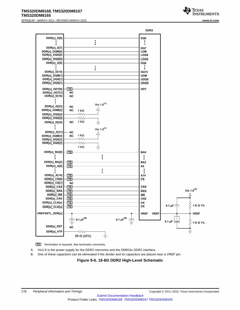
DDR[x]_D[0]
DDR[x]_D[7]
DDR[x]_DQM[0]
DDR[x]_DQS[0]
DDR[x]_DQS[0]
DDR[x]_D[8]
DDR[x]_D[15]
DDR[x]_DQM[1]
DDR[x]_DQS[1]
DDR[x]_DQS[1]
DQ0
DQ7
LDM
LDQS
LDQS
DQ8
DQ15
UDM
UDQS
UDQS
BA0
BA2
A0
A14
CS
CAS
RAS
WE
CKE
CK
CK
VREF
DDR[x]_D[16]
DDR[x]_D[23]
DDR[x]_DQM[2]
DDR[x]_DQS[2]
DDR[x]_DQS[2]
DDR[x]_D[24]
DDR[x]_D[31]
DDR[x]_DQM[3]
DDR[x]_DQS[3]
DDR[x]_DQS[3]
DDR[x]_BA[0]
DDR[x]_BA[2]
DDR[x]_A[0]
DDR[x]_A[14]
DDR[x]_CS[0]
DDR[x]_CAS
DDR[x]_RAS
DDR[x]_WE
DDR[x]_CKE
DDR[x]_CLK[x]
DDR[x]_CLK[x]
VREFSSTL_DDR[x]
1 K Ω 1%
Vio 1.8(A)
DDR2
VREF
0.1 µF
VREF
0.1 µF 1 K Ω 1%0.1 µF
(B)0.1 µF
(B)
DDR[x]_ODT[1] NC
ODT
NC
NC
NC
1 KΩ
NC
NC
1 KΩ
1 KΩ
1 KΩ
DDR[x]_VTP
50 ( 2%)Ω ±
Vio 1.8(A)
Vio 1.8(A)
T0
T0
T0
T0
T0
T0
T0
T0
T0
T0
T0
T0
T0 Termination is required. See terminator comments.
DDR[x]_ODT[0]
DDR[x]_CS[1] NC
DDR[x]_RST NC
NC
TMS320DM8168, TMS320DM8167TMS320DM8165SPRS614F –MARCH 2011–REVISED MARCH 2015 www.ti.com
A. Vio1.8 is the power supply for the DDR2 memories and the DM816x DDR2 interface.B. One of these capacitors can be eliminated if the divider and its capacitors are placed near a VREF pin.
Figure 9-6. 16-Bit DDR2 High-Level Schematic
178 Peripheral Information and Timings Copyright © 2011–2015, Texas Instruments IncorporatedSubmit Documentation Feedback
Product Folder Links: TMS320DM8168 TMS320DM8167 TMS320DM8165
TMS320DM8168, TMS320DM8167TMS320DM8165
www.ti.com SPRS614F –MARCH 2011–REVISED MARCH 2015
9.3.1.2.2 Compatible JEDEC DDR2 Devices
Table 9-2 shows the parameters of the JEDEC DDR2 devices that are compatible with this interface.Generally, the DDR2 interface is compatible with x16 DDR2-800 speed grade DDR2 devices.
Table 9-2. Compatible JEDEC DDR2 Devices
NO. PARAMETER MIN MAX UNIT1 JEDEC DDR2 device speed grade (1) DDR2-8002 JEDEC DDR2 device bit width x16 x16 Bits3 JEDEC DDR2 device count (2) 1 2 Devices4 JEDEC DDR2 device ball count (3) 84 92 Balls
(1) Higher DDR2 speed grades are supported due to inherent JEDEC DDR2 backwards compatibility.(2) One DDR2 device is used for a 16-bit DDR2 memory system. Two DDR2 devices are used for a 32-bit DDR2 memory system.(3) The 92-ball devices are retained for legacy support. New designs will migrate to 84-ball DDR2 devices. Electrically, the 92- and 84-ball
DDR2 devices are the same.
9.3.1.2.3 PCB Stackup
The minimum stackup required for routing the DM816x device is a six-layer stackup as shown in Table 9-3. Additional layers may be added to the PCB stackup to accommodate other circuitry or to reduce thesize of the PCB footprint.
Table 9-3. Minimum PCB Stackup
LAYER TYPE DESCRIPTION1 Signal Top routing mostly horizontal2 Plane Ground3 Plane Power4 Signal Internal routing5 Plane Ground6 Signal Bottom routing mostly vertical
Copyright © 2011–2015, Texas Instruments Incorporated Peripheral Information and Timings 179Submit Documentation Feedback
Product Folder Links: TMS320DM8168 TMS320DM8167 TMS320DM8165
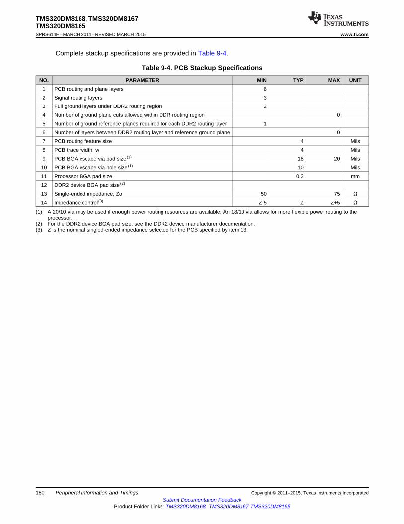
TMS320DM8168, TMS320DM8167TMS320DM8165SPRS614F –MARCH 2011–REVISED MARCH 2015 www.ti.com
Complete stackup specifications are provided in Table 9-4.
Table 9-4. PCB Stackup Specifications
NO. PARAMETER MIN TYP MAX UNIT1 PCB routing and plane layers 62 Signal routing layers 33 Full ground layers under DDR2 routing region 24 Number of ground plane cuts allowed within DDR routing region 05 Number of ground reference planes required for each DDR2 routing layer 16 Number of layers between DDR2 routing layer and reference ground plane 07 PCB routing feature size 4 Mils8 PCB trace width, w 4 Mils9 PCB BGA escape via pad size (1) 18 20 Mils10 PCB BGA escape via hole size (1) 10 Mils11 Processor BGA pad size 0.3 mm12 DDR2 device BGA pad size (2)
13 Single-ended impedance, Zo 50 75 Ω14 Impedance control (3) Z-5 Z Z+5 Ω
(1) A 20/10 via may be used if enough power routing resources are available. An 18/10 via allows for more flexible power routing to theprocessor.
(2) For the DDR2 device BGA pad size, see the DDR2 device manufacturer documentation.(3) Z is the nominal singled-ended impedance selected for the PCB specified by item 13.
180 Peripheral Information and Timings Copyright © 2011–2015, Texas Instruments IncorporatedSubmit Documentation Feedback
Product Folder Links: TMS320DM8168 TMS320DM8167 TMS320DM8165

A1A1
XRecommended DDR2 Device
Orientation
Y
DD
R2
Co
ntr
oller
X1
X1
OFFSET
X1
OFFSET
TMS320DM8168, TMS320DM8167TMS320DM8165
www.ti.com SPRS614F –MARCH 2011–REVISED MARCH 2015
9.3.1.2.4 Placement
Figure 9-7 shows the required placement for the processor as well as the DDR2 devices. The dimensionsfor this figure are defined in Table 9-5. The placement does not restrict the side of the PCB on which thedevices are mounted. The ultimate purpose of the placement is to limit the maximum trace lengths andallow for proper routing space. For a 16-bit DDR memory system, the high-word DDR2 device is omittedfrom the placement.
Figure 9-7. DM816x Device and DDR2 Device Placement
Table 9-5. Placement Specifications
NO. PARAMETER MIN MAX UNIT1 X + Y (1) (2) 1660 Mils2 X' (1) (2) 1280 Mils3 X' Offset (1) (2) (3) 650 Mils4 DDR2 keepout region (4)
5 Clearance from non-DDR2 signal to DDR2 keepout region (5) 4 w
(1) For dimension definitions, see Figure 9-5.(2) Measurements from center of processor to center of DDR2 device.(3) For 16-bit memory systems, it is recommended that X' offset be as small as possible.(4) DDR2 keepout region to encompass entire DDR2 routing area.(5) Non-DDR2 signals allowed within DDR2 keepout region provided they are separated from DDR2 routing layers by a ground plane.
Copyright © 2011–2015, Texas Instruments Incorporated Peripheral Information and Timings 181Submit Documentation Feedback
Product Folder Links: TMS320DM8168 TMS320DM8167 TMS320DM8165
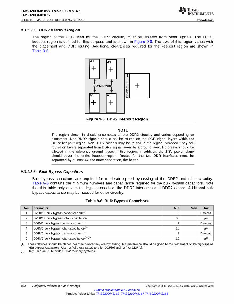
A1 A1
A1A1
DD
R2 C
on
tro
ller
DDR2 Device
TMS320DM8168, TMS320DM8167TMS320DM8165SPRS614F –MARCH 2011–REVISED MARCH 2015 www.ti.com
9.3.1.2.5 DDR2 Keepout Region
The region of the PCB used for the DDR2 circuitry must be isolated from other signals. The DDR2keepout region is defined for this purpose and is shown in Figure 9-8. The size of this region varies withthe placement and DDR routing. Additional clearances required for the keepout region are shown inTable 9-5.
Figure 9-8. DDR2 Keepout Region
NOTEThe region shown in should encompass all the DDR2 circuitry and varies depending onplacement. Non-DDR2 signals should not be routed on the DDR signal layers within theDDR2 keepout region. Non-DDR2 signals may be routed in the region, provided t hey arerouted on layers separated from DDR2 signal layers by a ground layer. No breaks should beallowed in the reference ground layers in this region. In addition, the 1.8V power planeshould cover the entire keepout region. Routes for the two DDR interfaces must beseparated by at least 4x; the more separation, the better.
9.3.1.2.6 Bulk Bypass Capacitors
Bulk bypass capacitors are required for moderate speed bypassing of the DDR2 and other circuitry.Table 9-6 contains the minimum numbers and capacitance required for the bulk bypass capacitors. Notethat this table only covers the bypass needs of the DDR2 interfaces and DDR2 device. Additional bulkbypass capacitance may be needed for other circuitry.
Table 9-6. Bulk Bypass Capacitors
No. Parameter Min Max Unit1 DVDD18 bulk bypass capacitor count (1) 6 Devices2 DVDD18 bulk bypass total capacitance 60 μF3 DDR#1 bulk bypass capacitor count (1) 1 Devices4 DDR#1 bulk bypass total capacitance (1) 10 μF5 DDR#2 bulk bypass capacitor count (2) 1 Devices6 DDR#2 bulk bypass total capacitance (1) (2) 10 μF
(1) These devices should be placed near the device they are bypassing, but preference should be given to the placement of the high-speed(HS) bypass capacitors. Use half of these capacitors for DDR[0] and half for DDR[1].
(2) Only used on 32-bit wide DDR2 memory systems.
182 Peripheral Information and Timings Copyright © 2011–2015, Texas Instruments IncorporatedSubmit Documentation Feedback
Product Folder Links: TMS320DM8168 TMS320DM8167 TMS320DM8165
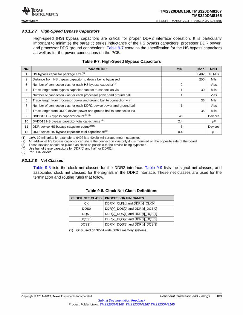
TMS320DM8168, TMS320DM8167TMS320DM8165
www.ti.com SPRS614F –MARCH 2011–REVISED MARCH 2015
9.3.1.2.7 High-Speed Bypass Capacitors
High-speed (HS) bypass capacitors are critical for proper DDR2 interface operation. It is particularlyimportant to minimize the parasitic series inductance of the HS bypass capacitors, processor DDR power,and processor DDR ground connections. Table 9-7 contains the specification for the HS bypass capacitorsas well as for the power connections on the PCB.
Table 9-7. High-Speed Bypass Capacitors
NO. PARAMETER MIN MAX UNIT1 HS bypass capacitor package size (1) 0402 10 Mils2 Distance from HS bypass capacitor to device being bypassed 250 Mils3 Number of connection vias for each HS bypass capacitor (2) 2 Vias4 Trace length from bypass capacitor contact to connection via 1 30 Mils5 Number of connection vias for each processor power and ground ball 1 Vias6 Trace length from processor power and ground ball to connection via 35 Mils7 Number of connection vias for each DDR2 device power and ground ball 1 Vias8 Trace length from DDR2 device power and ground ball to connection via 35 Mils9 DVDD18 HS bypass capacitor count (3) (4) 40 Devices10 DVDD18 HS bypass capacitor total capacitance (4) 2.4 μF11 DDR device HS bypass capacitor count (3) (5) 8 Devices12 DDR device HS bypass capacitor total capacitance (5) 0.4 μF
(1) LxW, 10-mil units; for example, a 0402 is a 40x20-mil surface-mount capacitor.(2) An additional HS bypass capacitor can share the connection vias only if it is mounted on the opposite side of the board.(3) These devices should be placed as close as possible to the device being bypassed.(4) Use half of these capacitors for DDR[0] and half for DDR[1].(5) Per DDR device.
9.3.1.2.8 Net Classes
Table 9-8 lists the clock net classes for the DDR2 interface. Table 9-9 lists the signal net classes, andassociated clock net classes, for the signals in the DDR2 interface. These net classes are used for thetermination and routing rules that follow.
Table 9-8. Clock Net Class Definitions
CLOCK NET CLASS PROCESSOR PIN NAMESCK DDR[x]_CLK[x] and DDR[x]_CLK[x]
DQS0 DDR[x]_DQS[0] and DDR[x]_DQS[0]DQS1 DDR[x]_DQS[1] and DDR[x]_DQS[1]
DQS2 (1) DDR[x]_DQS[2] and DDR[x]_DQS[2]DQS3 (1) DDR[x]_DQS[3] and DDR[x]_DQS[3]
(1) Only used on 32-bit wide DDR2 memory systems.
Copyright © 2011–2015, Texas Instruments Incorporated Peripheral Information and Timings 183Submit Documentation Feedback
Product Folder Links: TMS320DM8168 TMS320DM8167 TMS320DM8165

+ +
DDR2 Device
DDR2 Controller
VREF Bypass Capacitor
VREF Nominal Max Tracewidth is 20 mils
Neck down to minimum in BGA escape
regions is acceptable. Narrowing to
accomodate via congestion for short
distances is also acceptable. Best
performance is obtained if the width
of VREF is maximized.
A1 A1
TMS320DM8168, TMS320DM8167TMS320DM8165SPRS614F –MARCH 2011–REVISED MARCH 2015 www.ti.com
Table 9-9. Signal Net Class Definitions
ASSOCIATED CLOCKSIGNAL NET CLASS PROCESSOR PIN NAMESNET CLASSADDR_CTRL CK DDR[x]_BA[2:0], DDR[x]_A[14:0], DDR[x]_CS[x], DDR[x]_CAS, DDR[x]_RAS,
DDR[x]_WE, DDR[x]_CKE, DDR[x]_ODT[x]DQ0 DQS0 DDR[x]_D[7:0], DDR[x]_DQM[0]DQ1 DQS1 DDR[x]_D[15:8], DDR[x]_DQM[1]
DQ2 (1) DQS2 DDR[x]_D[23:16], DDR[x]_DQM[2]DQ3 (1) DQS3 DDR[x]_D[31:24], DDR[x]_DQM[3]
(1) Only used on 32-bit wide DDR2 memory systems.
9.3.1.2.9 DDR2 Signal Termination
Signal terminators are required in CK and ADDR_CTRL net classes. Serial terminators may be used ondata lines to reduce EMI risk; however, serial terminations are the only type permitted. ODT's areintegrated on the data byte net classes. They should be enabled to ensure signal integrity.Table 9-10shows the specifications for the series terminators.
Table 9-10. DDR2 Signal Terminations
NO. PARAMETER MIN TYP MAX UNIT1 CK net class (1) (2) 0 10 Ω2 ADDR_CTRL net class (1) (3) (4) (2) 0 22 Zo Ω3 Data byte net classes (DQS0-DQS3, DQ0-DQ3) (5) 0 0 Ω
(1) Only series termination is permitted, parallel or SST specifically disallowed on board.(2) Only required for EMI reduction.(3) Terminator values larger than typical only recommended to address EMI issues.(4) Termination value should be uniform across net class.(5) No external terminations allowed for data byte net classes. ODT is to be used.
9.3.1.2.10 VREFSSTL_DDR Routing
VREFSSTL_DDR is used as a reference by the input buffers of the DDR2 memories as well as theprocessor. VREF is intended to be half the DDR2 power supply voltage and should be created using aresistive divider as shown in Figure 9-6. Other methods of creating VREF are not recommended. Figure 9-9 shows the layout guidelines for VREF.
Figure 9-9. VREF Routing and Topology
184 Peripheral Information and Timings Copyright © 2011–2015, Texas Instruments IncorporatedSubmit Documentation Feedback
Product Folder Links: TMS320DM8168 TMS320DM8167 TMS320DM8165

A1E0
T
E1T
E2
E3T
DD
R2
Co
ntr
oller
T A1
A1 A1
CB
A´´
T
DD
R2
Co
ntr
oller
A = A´ + A´´
A´
TMS320DM8168, TMS320DM8167TMS320DM8165
www.ti.com SPRS614F –MARCH 2011–REVISED MARCH 2015
9.3.1.3 DDR2 CK and ADDR_CTRL Routing
Figure 9-10 shows the topology of the routing for the CK and ADDR_CTRL net classes. The route is abalanced T as it is intended that the length of segments B and C be equal. In addition, the length of A(A'+A'') should be maximized.
Figure 9-10. CK and ADDR_CTRL Routing and Topology
Table 9-11. CK and ADDR_CTRL Routing Specification (1)
NO. PARAMETER MIN TYP MAX UNIT
1 Center-to-center CK-CK spacing 2w
2 CK and CK skew (1) 25 Mils
3 CK B-to-C skew length mismatch 25 Mils
4 Center-to-center CK to other DDR2 trace spacing (2) 4w
5 CK and ADDR_CTRL nominal trace length (3) CACLM-50 CACLM CACLM+50 Mils
6 ADDR_CTRL-to-CK skew length mismatch 100 Mils
7 ADDR_CTRL-to-ADDR_CTRL skew length mismatch 100 Mils
8 Center-to-center ADDR_CTRL to other DDR2 trace spacing (2) 4w
9 Center-to-center ADDR_CTRL to other ADDR_CTRL trace spacing (2) 3w
10 ADDR_CTRL B-to-C skew length mismatch 100 Mils
(1) The length of segment A=A'+A′′ as shown in Figure 9-10.(2) Center-to-center spacing is allowed to fall to minimum (w) for up to 500 mils of routed length to accommodate BGA escape and routing
congestion.(3) CACLM is the longest Manhattan distance of the CK and ADDR_CTRL net classes.
Figure 9-11 shows the topology and routing for the DQS and DQ net classes; the routes are point to point.Skew matching across bytes is not needed nor recommended.
Figure 9-11. DQS and DQ Routing and Toplogy
Copyright © 2011–2015, Texas Instruments Incorporated Peripheral Information and Timings 185Submit Documentation Feedback
Product Folder Links: TMS320DM8168 TMS320DM8167 TMS320DM8165

DDR_CLK
1
TMS320DM8168, TMS320DM8167TMS320DM8165SPRS614F –MARCH 2011–REVISED MARCH 2015 www.ti.com
Table 9-12. DQS and DQ Routing Specification
NO. PARAMETER MIN TYP MAX UNIT1 Center-to-center DQS-DQSn spacing in E0|E1|E2|E3 2w2 DQS-DQSn skew in E0|E1|E2|E3 25 Mils3 Center-to-center DQS to other DDR2 trace spacing (1) 4w4 DQS and DQ nominal trace length (2) (3) (4) DQLM-50 DQLM DQLM+50 Mils5 DQ-to-DQS skew length mismatch (2) (3) (4) 100 Mils6 DQ-to-DQ skew length mismatch (2) (3) (4) 100 Mils7 DQ-to-DQ and DQS via count mismatch (2) (3) (4) 1 Vias8 Center-to-center DQ to other DDR2 trace spacing (1) (5) 4w9 Center-to-center DQ to other DQ trace spacing (1) (6) (7) 3w10 DQ and DQS E skew length mismatch (2) (3) (4) 100 Mils
(1) Center-to-center spacing is allowed to fall to minimum (w) for up to 500 mils of routed length to accommodate BGA escape and routingcongestion.
(2) A 16-bit DDR memory system has two sets of data net classes; one for data byte 0, and one for data byte 1, each with an associatedDQS (2 DQSs) per DDR EMIF used.
(3) A 32-bit DDR memory system has four sets of data net classes; one each for data bytes 0 through 3, and each associated with a DQS(4 DQSs) per DDR EMIF used.
(4) There is no need, and it is not recommended, to skew match across data bytes; that is, from DQS0 and data byte 0 to DQS1 and databyte 1.
(5) DQs from other DQS domains are considered other DDR2 trace.(6) DQs from other data bytes are considered other DDR2 trace.(7) DQLM is the longest Manhattan distance of each of the DQS and DQ net classes.
9.3.2 DDR3 Routing Specifications
9.3.2.1 Board Designs
TI only supports board designs utilizing DDR3 memory that follow the specifications in this document. Theswitching characteristics and timing diagram for the DDR3 memory controller are shown in Table 9-13 andFigure 9-12.
Table 9-13. Switching Characteristics Over Recommended Operating Conditions for DDR3 MemoryController
-1GNO. PARAMETER UNIT
MIN MAX1 tc(DDR_CLK) Cycle time, DDR_CLK 1.25 3.3 (1) ns
(1) This is the absolute maximum the clock period can be. Actual maximum clock period may be limited by DDR3 speed grade andoperating frequency (see the DDR3 memory device data sheet).
Figure 9-12. DDR3 Memory Controller Clock Timing
9.3.2.1.1 DDR3 versus DDR2
This specification only covers TMS320DM816x processor PCB designs that utilize DDR3 memory.Designs using DDR2 memory should use the PCB design specifications for DDR2 memory inSection 9.3.1. While similar, the two memory systems have different requirements. It is currently notpossible to design one PCB that covers both DDR2 and DDR3.
9.3.2.2 DDR3 Device Combinations
Since there are several possible combinations of device counts and single- or dual-side mounting,Table 9-14 summarizes the supported device configurations.
186 Peripheral Information and Timings Copyright © 2011–2015, Texas Instruments IncorporatedSubmit Documentation Feedback
Product Folder Links: TMS320DM8168 TMS320DM8167 TMS320DM8165
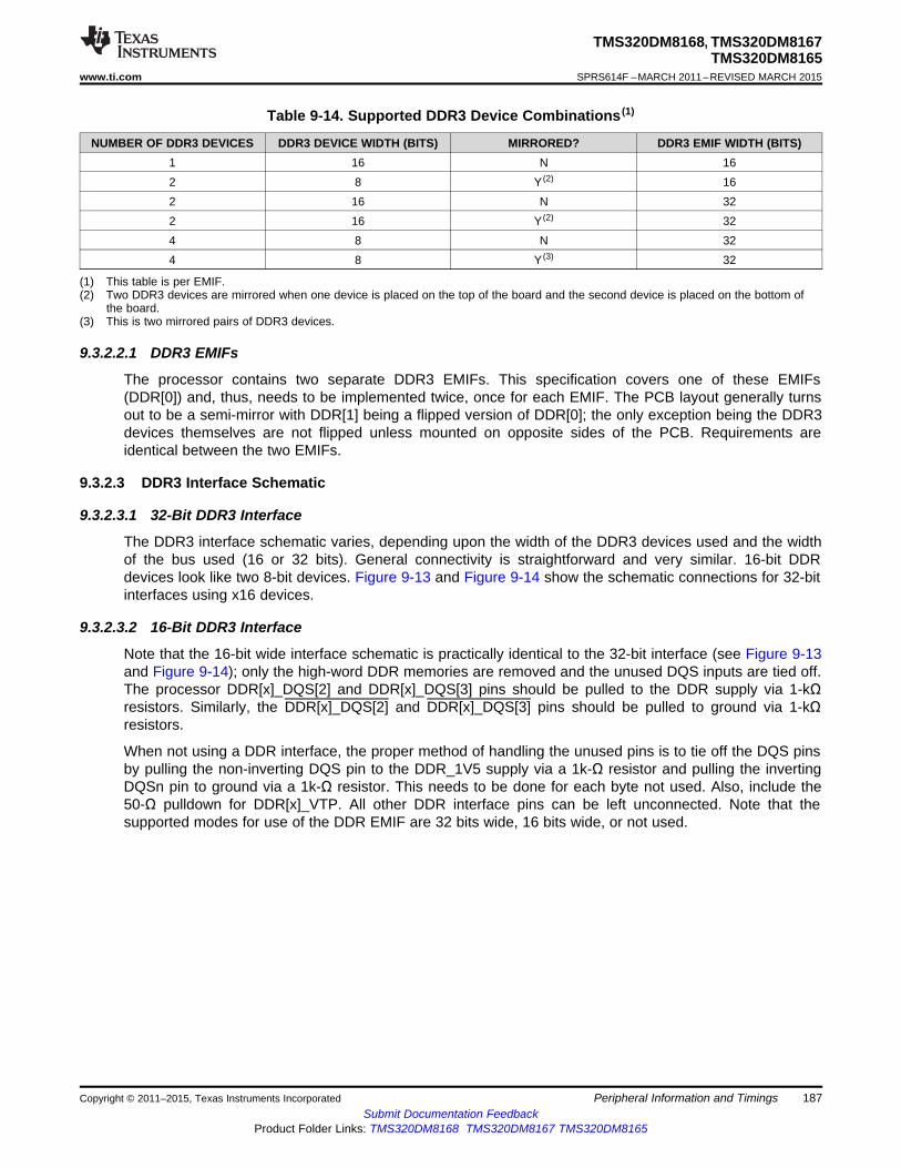
TMS320DM8168, TMS320DM8167TMS320DM8165
www.ti.com SPRS614F –MARCH 2011–REVISED MARCH 2015
Table 9-14. Supported DDR3 Device Combinations (1)
NUMBER OF DDR3 DEVICES DDR3 DEVICE WIDTH (BITS) MIRRORED? DDR3 EMIF WIDTH (BITS)1 16 N 162 8 Y (2) 162 16 N 322 16 Y (2) 324 8 N 324 8 Y (3) 32
(1) This table is per EMIF.(2) Two DDR3 devices are mirrored when one device is placed on the top of the board and the second device is placed on the bottom of
the board.(3) This is two mirrored pairs of DDR3 devices.
9.3.2.2.1 DDR3 EMIFs
The processor contains two separate DDR3 EMIFs. This specification covers one of these EMIFs(DDR[0]) and, thus, needs to be implemented twice, once for each EMIF. The PCB layout generally turnsout to be a semi-mirror with DDR[1] being a flipped version of DDR[0]; the only exception being the DDR3devices themselves are not flipped unless mounted on opposite sides of the PCB. Requirements areidentical between the two EMIFs.
9.3.2.3 DDR3 Interface Schematic
9.3.2.3.1 32-Bit DDR3 Interface
The DDR3 interface schematic varies, depending upon the width of the DDR3 devices used and the widthof the bus used (16 or 32 bits). General connectivity is straightforward and very similar. 16-bit DDRdevices look like two 8-bit devices. Figure 9-13 and Figure 9-14 show the schematic connections for 32-bitinterfaces using x16 devices.
9.3.2.3.2 16-Bit DDR3 Interface
Note that the 16-bit wide interface schematic is practically identical to the 32-bit interface (see Figure 9-13and Figure 9-14); only the high-word DDR memories are removed and the unused DQS inputs are tied off.The processor DDR[x]_DQS[2] and DDR[x]_DQS[3] pins should be pulled to the DDR supply via 1-kΩresistors. Similarly, the DDR[x]_DQS[2] and DDR[x]_DQS[3] pins should be pulled to ground via 1-kΩresistors.
When not using a DDR interface, the proper method of handling the unused pins is to tie off the DQS pinsby pulling the non-inverting DQS pin to the DDR_1V5 supply via a 1k-Ω resistor and pulling the invertingDQSn pin to ground via a 1k-Ω resistor. This needs to be done for each byte not used. Also, include the50-Ω pulldown for DDR[x]_VTP. All other DDR interface pins can be left unconnected. Note that thesupported modes for use of the DDR EMIF are 32 bits wide, 16 bits wide, or not used.
Copyright © 2011–2015, Texas Instruments Incorporated Peripheral Information and Timings 187Submit Documentation Feedback
Product Folder Links: TMS320DM8168 TMS320DM8167 TMS320DM8165

DDR[x]_CLK[1]
DQ15
DQ8
UDM
UDQS
UDQS
DQ7
DQ0
LDM
LDQS
LDQS
CK
DQ15
UDM
UDQS
UDQS
DDR[x]_D[31]
DDR[x]_D[24]
16-Bit DDR3Devices
0.1 µF
NC
50 2Ω (± %)
0.1 µF 0.1 µF
32-bit DDR3 EMIFDDR[0] or DDR[1]
DDR[x]_CLK[1]
DDR[x]_ODT[1]
DDR[x]_CS[1]
DDR[x]_DQM[3]
DDR[x]_DQS[3]
DDR[x]_DQS[3]
DDR[x]_D[23]
DDR[x]_D[16]
DDR[x]_DQM[2]
DDR[x]_DQS[2]
DDR[x]_DQS[2]
DDR[x]_D[15]
DDR[x]_D[8]
DDR[x]_DQM[1]
DDR[x]_DQS[1]
DDR[x]_DQS[1]
DDR[x]_D[7]
DDR[x]_D[0]
DDR[x]_DQM[0]
DDR[x]_DQS[0]
DDR[x]_DQS[0]
DDR[x]_CLK[0]
DDR[x]_CLK[0]
DDR[x]_ODT[0]
DDR[x]_CS[0]DDR[x]_BA[0]
DDR[x]_BA[1]
DDR[x]_BA[2]
DDR[x]_A[0]
DDR[x]_A[14]
DDR[x]_CAS
DDR[x]_RAS
DDR[x]_WE
DDR[x]_CKE
DDR[x]_RST
VREFSSTL_DDR[x]
DDR[x]_VTP
NC
NC
NC
8
8
8
8
15
DQ8
DQ7
D08
LDM
LDQS
LDQS
CK
ODT
BA1
BA0
BA2
CS
A0
A14
CAS
RAS
WE
RST
CKE
ZQ
VREFDQ
VREFCA
ZQ
CK
CK
ODT
BA1
BA0
BA2
CS
A0
A14
CAS
RAS
WE
RST
CKE
ZQ
VREFDQ
VREFCA
ZQ
Zo
Zo
Zo
Zo
DDR_VREF
DDR_VTT
DDR_1V5
Termination is required. See terminator comments.Zo
Value determined according to the DDR memory device data sheet.ZQ
0.1 µF
TMS320DM8168, TMS320DM8167TMS320DM8165SPRS614F –MARCH 2011–REVISED MARCH 2015 www.ti.com
Figure 9-13. 32-Bit, One-Bank DDR3 Interface Schematic Using Two 16-Bit DDR3 Devices
188 Peripheral Information and Timings Copyright © 2011–2015, Texas Instruments IncorporatedSubmit Documentation Feedback
Product Folder Links: TMS320DM8168 TMS320DM8167 TMS320DM8165

DDR[x]_CLK[1]
DQ7
DQ0
DM/TQS
DQS
DQS
DQ7
DQ0
DM/TQS
DQS
DQS
CK
DDR[x]_D[31]
DDR[x]_D[24]
8-Bit DDR3Devices
0.1 µF
NC
50 2Ω (± %)
0.1 µF 0.1 µF
32-bit DDR3 EMIFDDR[0] or DDR[1]
DDR[x]_CLK[1]
DDR[x]_ODT[1]
DDR[x]_CS[1]
DDR[x]_DQM[3]
DDR[x]_DQS[3]
DDR[x]_DQS[3]
DDR[x]_D[23]
DDR[x]_D[16]
DDR[x]_DQM[2]
DDR[x]_DQS[2]
DDR[x]_DQS[2]
DDR[x]_D[15]
DDR[x]_D[8]
DDR[x]_DQM[1]
DDR[x]_DQS[1]
DDR[x]_DQS[1]
DDR[x]_D[7]
DDR[x]_D[0]
DDR[x]_DQM[0]
DDR[x]_DQS[0]
DDR[x]_DQS[0]
DDR[x]_CLK[0]
DDR[x]_CLK[0]
DDR[x]_ODT[0]
DDR[x]_CS[0]DDR[x]_BA[0]
DDR[x]_BA[1]
DDR[x]_BA[2]
DDR[x]_A[0]
DDR[x]_A[14]
DDR[x]_CAS
DDR[x]_RAS
DDR[x]_WE
DDR[x]_CKE
DDR[x]_RST
VREFSSTL_DDR[x]
DDR[x]_VTP
NC
NC
NC
8
8
8
8
15
CK
ODT
BA1
BA0
BA2
CS
A0
A14
CAS
RAS
WE
RST
CKE
ZQ
VREFDQ
VREFCA
ZQ
CK
CK
ODT
BA1
BA0
BA2
CS
A0
A14
CAS
RAS
WE
RST
CKE
ZQ
VREFDQ
VREFCA
Termination is required. See terminator comments.Zo
Value determined according to the DDR memory device data sheet.ZQ
DQ7
DQ0
DM/TQS
DQS
DQS
CK
DQ7
DM/TQS
DQS
DQS
8-Bit DDR3Devices
0.1 µF 0.1 µF
DQ0
CK
ODT
BA1
BA0
BA2
CS
A0
A14
CAS
RAS
WE
RST
CKE
ZQ
VREFDQ
VREFCA
CK
CK
ODT
BA1
BA0
BA2
CS
A0
A14
CAS
RAS
WE
RST
CKE
ZQ
VREFDQ
VREFCA
ZQ
Zo
Zo
Zo
Zo
DDR_VREF
DDR_VTT
DDR_1V5
ZQ ZQ
TDQSNC
NC TDQS
TDQSNC
TDQSNC
0.1 µF
TMS320DM8168, TMS320DM8167TMS320DM8165
www.ti.com SPRS614F –MARCH 2011–REVISED MARCH 2015
Figure 9-14. 32-Bit, One-Bank DDR3 Interface Schematic Using Four 8-Bit DDR3 Devices
Copyright © 2011–2015, Texas Instruments Incorporated Peripheral Information and Timings 189Submit Documentation Feedback
Product Folder Links: TMS320DM8168 TMS320DM8167 TMS320DM8165

TMS320DM8168, TMS320DM8167TMS320DM8165SPRS614F –MARCH 2011–REVISED MARCH 2015 www.ti.com
9.3.2.4 Compatible JEDEC DDR3 Devices
Table 9-15 shows the parameters of the JEDEC DDR3 devices that are compatible with this interface.Generally, the DDR3 interface is compatible with DDR3-1600 devices in the x8 or x16 widths.
Table 9-15. Compatible JEDEC DDR3 Devices
NO. PARAMETER MIN MAX UNIT1 JEDEC DDR3 device speed grade (1) DDR3-800 DDR3-16002 JEDEC DDR3 device bit width x8 x16 Bits3 JEDEC DDR3 device count (2) 2 8 Devices
(1) DDR3 speed grade depends on desired clock rate. Data rate is 2x the clock rate. For DDR3-1600, the clock rate is 800 MHz.(2) For valid DDR3 device configurations and device counts, see Section 9.3.2.3, Figure 9-13, and Figure 9-14.
9.3.2.5 PCB Stackup
The minimum stackup for routing the DDR3 interface is a four-layer stack up as shown in Table 9-16.Additional layers may be added to the PCB stackup to accommodate other circuitry, enhance SI and EMIperformance, or to reduce the size of the PCB footprint. A six-layer stackup is shown in Table 9-17.Complete stackup specifications are provided in Table 9-18.
Table 9-16. Minimum PCB Stackup
LAYER TYPE DESCRIPTION1 Signal Top routing mostly vertical2 Plane Split power plane3 Plane Full ground plane4 Signal Bottom routing mostly horizontal
Table 9-17. Six-Layer PCB Stackup Suggestion
LAYER TYPE DESCRIPTION1 Signal Top routing mostly vertical2 Plane Ground3 Plane Split power plane4 Plane Split power plane or Internal routing5 Plane Ground6 Signal Bottom routing mostly horizontal
190 Peripheral Information and Timings Copyright © 2011–2015, Texas Instruments IncorporatedSubmit Documentation Feedback
Product Folder Links: TMS320DM8168 TMS320DM8167 TMS320DM8165

DDR3
Controller
Y
X1
X2 X2 X2
TMS320DM8168, TMS320DM8167TMS320DM8165
www.ti.com SPRS614F –MARCH 2011–REVISED MARCH 2015
Table 9-18. PCB Stackup Specifications
NO. PARAMETER MIN TYP MAX UNIT1 PCB routing and plane layers 4 62 Signal routing layers 23 Full ground reference layers under DDR3 routing region (1) 14 Full 1.5-V power reference layers under the DDR3 routing region (1) 15 Number of reference plane cuts allowed within DDR routing region (2) 06 Number of layers between DDR3 routing layer and reference plane (3) 07 PCB routing feature size 4 Mils8 PCB trace width, w 4 Mils9 PCB BGA escape via pad size (4) 18 20 Mils10 PCB BGA escape via hole size 10 Mils11 Processor BGA pad size 0.3 mm12 DDR3 device BGA pad size (5)
13 Single-ended impedance, Zo 50 75 Ω14 Impedance control (6) Z-5 Z Z+5 Ω
(1) Ground reference layers are preferred over power reference layers. Be sure to include bypass caps to accommodate reference layerreturn current as the trace routes switch routing layers.
(2) No traces should cross reference plane cuts within the DDR routing region. High-speed signal traces crossing reference plane cutscreate large return current paths which can lead to excessive crosstalk and EMI radiation.
(3) Reference planes are to be directly adjacent to the signal plane to minimize the size of the return current loop.(4) An 18-mil pad assumes Via Channel is the most economical BGA escape. A 20-mil pad may be used if additional layers are available
for power routing. An 18-mil pad is required for minimum layer count escape.(5) For the DDR3 device BGA pad size, see the DDR3 device manufacturer documentation.(6) Z is the nominal singled-ended impedance selected for the PCB specified by item 13.
9.3.2.6 Placement
Figure 9-15 shows the required placement for the processor as well as the DDR3 devices. Thedimensions for this figure are defined in Table 9-19. The placement does not restrict the side of the PCBon which the devices are mounted. The ultimate purpose of the placement is to limit the maximum tracelengths and allow for proper routing space. For a 16-bit DDR memory system, the high-word DDR3devices are omitted from the placement.
Figure 9-15. Placement Specifications
Copyright © 2011–2015, Texas Instruments Incorporated Peripheral Information and Timings 191Submit Documentation Feedback
Product Folder Links: TMS320DM8168 TMS320DM8167 TMS320DM8165
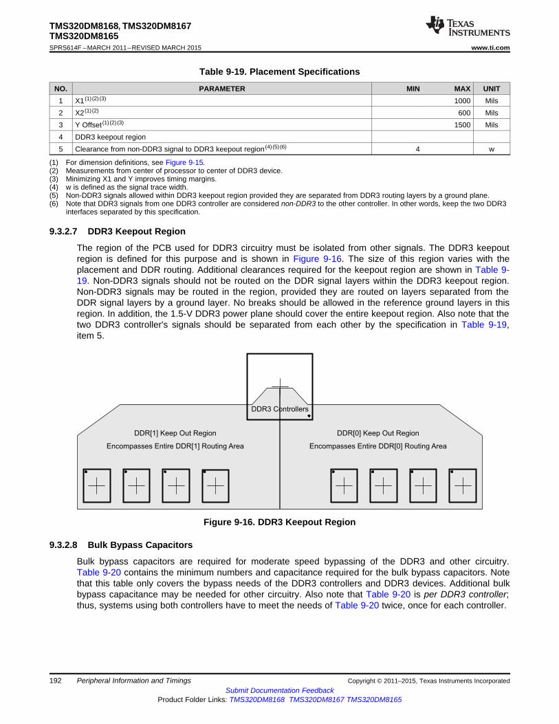
DDR[0] Keep Out Region
Encompasses Entire DDR[0] Routing Area
DDR3 Controllers
DDR[1] Keep Out Region
Encompasses Entire DDR[1] Routing Area
TMS320DM8168, TMS320DM8167TMS320DM8165SPRS614F –MARCH 2011–REVISED MARCH 2015 www.ti.com
Table 9-19. Placement Specifications
NO. PARAMETER MIN MAX UNIT1 X1 (1) (2) (3) 1000 Mils2 X2 (1) (2) 600 Mils3 Y Offset (1) (2) (3) 1500 Mils4 DDR3 keepout region5 Clearance from non-DDR3 signal to DDR3 keepout region (4) (5) (6) 4 w
(1) For dimension definitions, see Figure 9-15.(2) Measurements from center of processor to center of DDR3 device.(3) Minimizing X1 and Y improves timing margins.(4) w is defined as the signal trace width.(5) Non-DDR3 signals allowed within DDR3 keepout region provided they are separated from DDR3 routing layers by a ground plane.(6) Note that DDR3 signals from one DDR3 controller are considered non-DDR3 to the other controller. In other words, keep the two DDR3
interfaces separated by this specification.
9.3.2.7 DDR3 Keepout Region
The region of the PCB used for DDR3 circuitry must be isolated from other signals. The DDR3 keepoutregion is defined for this purpose and is shown in Figure 9-16. The size of this region varies with theplacement and DDR routing. Additional clearances required for the keepout region are shown in Table 9-19. Non-DDR3 signals should not be routed on the DDR signal layers within the DDR3 keepout region.Non-DDR3 signals may be routed in the region, provided they are routed on layers separated from theDDR signal layers by a ground layer. No breaks should be allowed in the reference ground layers in thisregion. In addition, the 1.5-V DDR3 power plane should cover the entire keepout region. Also note that thetwo DDR3 controller's signals should be separated from each other by the specification in Table 9-19,item 5.
Figure 9-16. DDR3 Keepout Region
9.3.2.8 Bulk Bypass Capacitors
Bulk bypass capacitors are required for moderate speed bypassing of the DDR3 and other circuitry.Table 9-20 contains the minimum numbers and capacitance required for the bulk bypass capacitors. Notethat this table only covers the bypass needs of the DDR3 controllers and DDR3 devices. Additional bulkbypass capacitance may be needed for other circuitry. Also note that Table 9-20 is per DDR3 controller;thus, systems using both controllers have to meet the needs of Table 9-20 twice, once for each controller.
192 Peripheral Information and Timings Copyright © 2011–2015, Texas Instruments IncorporatedSubmit Documentation Feedback
Product Folder Links: TMS320DM8168 TMS320DM8167 TMS320DM8165

TMS320DM8168, TMS320DM8167TMS320DM8165
www.ti.com SPRS614F –MARCH 2011–REVISED MARCH 2015
Table 9-20. Bulk Bypass Capacitors
NO. PARAMETER MIN MAX UNIT1 DDR_1V5 bulk bypass capacitor count (1) 6 Devices2 DDR_1V5 bulk bypass total capacitance 140 μF
(1) These devices should be placed near the devices they are bypassing, but preference should be given to the placement of the high-speed (HS) bypass capacitors and DDR3 signal routing.
9.3.2.9 High-Speed Bypass Capacitors
High-speed (HS) bypass capacitors are critical for proper DDR3 interface operation. It is particularlyimportant to minimize the parasitic series inductance of the HS bypass capacitors, processor DDR power,and processor DDR ground connections. Table 9-21 contains the specification for the HS bypasscapacitors as well as for the power connections on the PCB. Generally speaking, it is good to:1. Fit as many HS bypass capacitors as possible.2. Minimize the distance from the bypass cap to the pins (balls) being bypassed.3. Use the smallest physical sized capacitors possible with the highest capacitance readily available.4. Connect the bypass capacitor pads to their vias using the widest traces possible and using the largest
hole size via possible.5. Minimize via sharing. Note the limits on via sharing shown in Table 9-21.
Table 9-21. High-Speed Bypass Capacitors
NO. PARAMETER MIN TYP MAX UNIT1 HS bypass capacitor package size (1) 201 402 10 Mils2 Distance, HS bypass capacitor to processor being bypassed (2) (3) (4) 400 Mils3 Processor DDR_1V5 HS bypass capacitor count 70 Devices4 Processor DDR_1V5 HS bypass capacitor total capacitance 5 μF5 Number of connection vias for each device power and ground ball (5) Vias6 Trace length from device power and ground ball to connection via (2) 35 70 Mils7 Distance, HS bypass capacitor to DDR device being bypassed (6) 150 Mils8 DDR3 device HS bypass capacitor count (7) 12 Devices9 DDR3 device HS bypass capacitor total capacitance (7) 0.85 μF10 Number of connection vias for each HS capacitor (8) (9) 2 Vias11 Trace length from bypass capacitor connect to connection via (2) (9) 35 100 Mils12 Number of connection vias for each DDR3 device power and ground 1 Vias
ball (10)
13 Trace length from DDR3 device power and ground ball to connection 35 60 Milsvia (2) (8)
(1) LxW, 10-mil units, for example, a 0402 is a 40x20-mil surface-mount capacitor.(2) Closer and shorter is better.(3) Measured from the nearest processor power and ground ball to the center of the capacitor package.(4) Three of these capacitors should be located underneath the processor, between the cluster of DDR_1V5 balls and ground balls,
between the DDR interfaces on the package.(5) See the Via Channel™ escape for the processor package.(6) Measured from the DDR3 device power and ground ball to the center of the capacitor package.(7) Per DDR3 device.(8) An additional HS bypass capacitor can share the connection vias only if it is mounted on the opposite side of the board. No sharing of
vias is permitted on the same side of the board.(9) An HS bypass capacitor may share a via with a DDR device mounted on the same side of the PCB. A wide trace should be used for the
connection and the length from the capacitor pad to the DDR device pad should be less than 150 mils.(10) Up to a total of two pairs of DDR power and ground balls may share a via.
Copyright © 2011–2015, Texas Instruments Incorporated Peripheral Information and Timings 193Submit Documentation Feedback
Product Folder Links: TMS320DM8168 TMS320DM8167 TMS320DM8165
TMS320DM8168, TMS320DM8167TMS320DM8165SPRS614F –MARCH 2011–REVISED MARCH 2015 www.ti.com
9.3.2.9.1 Return Current Bypass Capacitors
Use additional bypass capacitors if the return current reference plane changes due to DDR3 signalshopping from one signal layer to another. The bypass capacitor here provides a path for the return currentto hop planes along with the signal. As many of these return current bypass capacitors should be used aspossible. Since these are returns for signal current, the signal via size may be used for these capacitors.
9.3.2.10 Net Classes
Table 9-22 lists the clock net classes for the DDR3 interface. Table 9-23 lists the signal net classes, andassociated clock net classes, for signals in the DDR3 interface. These net classes are used for thetermination and routing rules that follow.
Table 9-22. Clock Net Class Definitions
CLOCK NET CLASS PROCESSOR PIN NAMESCK DDR[x]_CLK[x] and DDR[x]_CLK[x]
DQS0 DDR[x]_DQS[0] and DDR[x]_DQS[0]DQS1 DDR[x]_DQS[1] and DDR[x]_DQS[1]
DQS2 (1) DDR[x]_DQS[2] and DDR[x]_DQS[2]DQS3 (1) DDR[x]_DQS[3] and DDR[x]_DQS[3]
(1) Only used on 32-bit wide DDR3 memory systems.
Table 9-23. Signal Net Class Definitions
ASSOCIATED CLOCKSIGNAL NET CLASS PROCESSOR PIN NAMESNET CLASSADDR_CTRL CK DDR[x]_BA[2:0], DDR[x]_A[14:0], DDR[x]_CS[x], DDR[x]_CAS, DDR[x]_RAS,
DDR[x]_WE, DDR[x]_CKE, DDR[x]_ODT[x]DQ0 DQS0 DDR[x]_D[7:0], DDR[x]_DQM[0]DQ1 DQS1 DDR[x]_D[15:8], DDR[x]_DQM[1]
DQ2 (1) DQS2 DDR[x]_D[23:16], DDR[x]_DQM[2]DQ3 (1) DQS3 DDR[x]_D[31:24], DDR[x]_DQM[3]
(1) Only used on 32-bit wide DDR3 memory systems.
9.3.2.11 DDR3 Signal Termination
Signal terminators are required for the CK and ADDR_CTRL net classes. The data lines are terminated byODT and, thus, the PCB traces should be unterminated. Detailed termination specifications are covered inthe routing rules in the following sections.
9.3.2.12 VREFSSTL_DDR Routing
VREFSSTL_DDR (VREF) is used as a reference by the input buffers of the DDR3 memories as well asthe processor. VREF is intended to be half the DDR3 power supply voltage and is typically generated withthe DDR3 1.5-V and VTT power supply. It should be routed as a nominal 20-mil wide trace with 0.1 µFbypass capacitors near each device connection. Narrowing of VREF is allowed to accommodate routingcongestion.
9.3.2.13 VTT
Like VREF, the nominal value of the VTT supply is half the DDR3 supply voltage. Unlike VREF, VTT isexpected to source and sink current, specifically the termination current for the ADDR_CTRL net classThevinen terminators. VTT is needed at the end of the address bus and it should be routed as a powersub-plane. VTT should be bypassed near the terminator resistors.
194 Peripheral Information and Timings Copyright © 2011–2015, Texas Instruments IncorporatedSubmit Documentation Feedback
Product Folder Links: TMS320DM8168 TMS320DM8167 TMS320DM8165
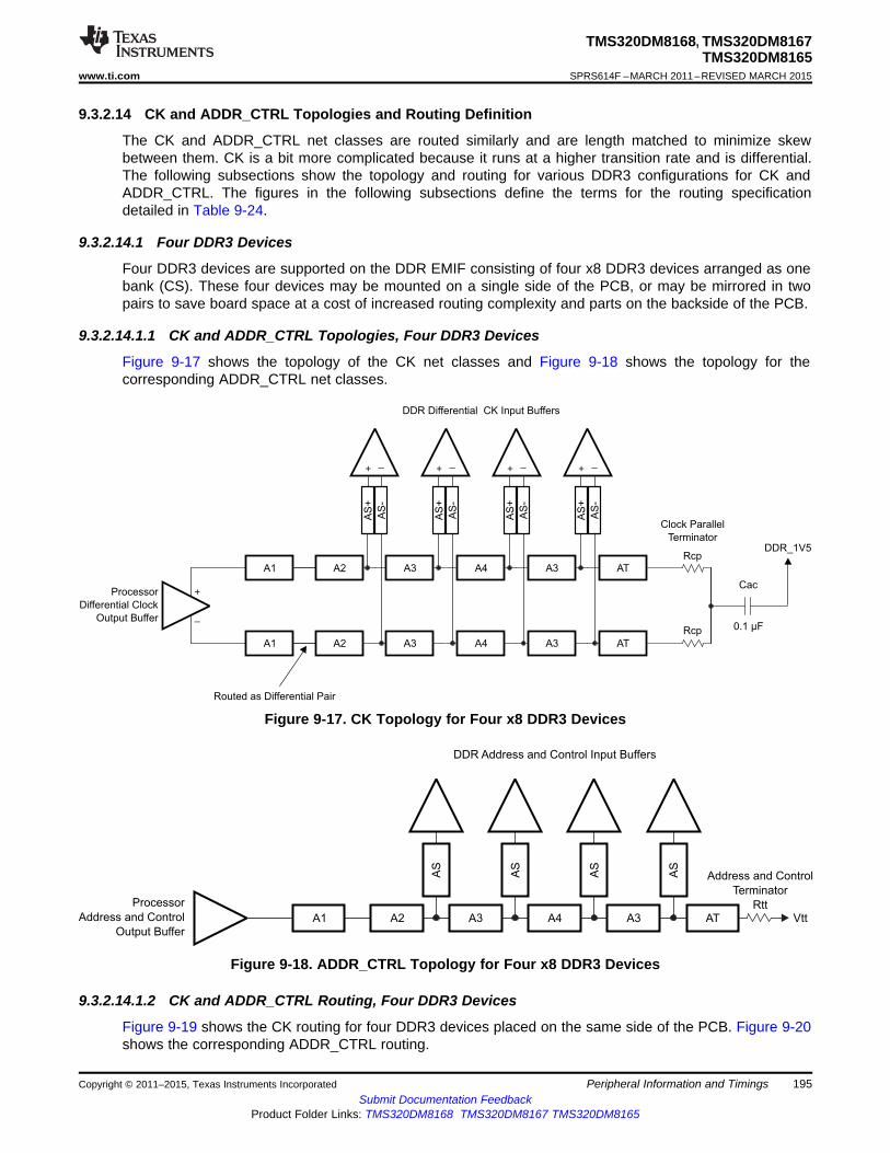
A1 A2
Processor
Address and Control
Output Buffer
DDR Address and Control Input Buffers
A3 A4 A3 AT Vtt
Address and Control
Terminator
Rtt
AS
AS
AS
AS
AS
-
AS
+
AS
-
AS
+
AS
-
AS
+
A1 A2
Processor
Differential Clock
Output Buffer
DDR Differential CK Input Buffers
Routed as Differential Pair
A3 A4 A3 AT
Rcp
Clock Parallel
Terminator
A1 A2 A3 A4 A3 AT
AS
-
AS
+
Rcp
Cac
DDR_1V5
0.1 µF
+
–
+ – + – + – + –
TMS320DM8168, TMS320DM8167TMS320DM8165
www.ti.com SPRS614F –MARCH 2011–REVISED MARCH 2015
9.3.2.14 CK and ADDR_CTRL Topologies and Routing Definition
The CK and ADDR_CTRL net classes are routed similarly and are length matched to minimize skewbetween them. CK is a bit more complicated because it runs at a higher transition rate and is differential.The following subsections show the topology and routing for various DDR3 configurations for CK andADDR_CTRL. The figures in the following subsections define the terms for the routing specificationdetailed in Table 9-24.
9.3.2.14.1 Four DDR3 Devices
Four DDR3 devices are supported on the DDR EMIF consisting of four x8 DDR3 devices arranged as onebank (CS). These four devices may be mounted on a single side of the PCB, or may be mirrored in twopairs to save board space at a cost of increased routing complexity and parts on the backside of the PCB.
9.3.2.14.1.1 CK and ADDR_CTRL Topologies, Four DDR3 Devices
Figure 9-17 shows the topology of the CK net classes and Figure 9-18 shows the topology for thecorresponding ADDR_CTRL net classes.
Figure 9-17. CK Topology for Four x8 DDR3 Devices
Figure 9-18. ADDR_CTRL Topology for Four x8 DDR3 Devices
9.3.2.14.1.2 CK and ADDR_CTRL Routing, Four DDR3 Devices
Figure 9-19 shows the CK routing for four DDR3 devices placed on the same side of the PCB. Figure 9-20shows the corresponding ADDR_CTRL routing.
Copyright © 2011–2015, Texas Instruments Incorporated Peripheral Information and Timings 195Submit Documentation Feedback
Product Folder Links: TMS320DM8168 TMS320DM8167 TMS320DM8165

AS=
Rtt
A1
A2 A3 A4 A3 AT Vtt
AS
+
AS
-
=
Rcp
Rcp
Cac
DDR_1V5
0.1 µF
A1
A2 A3 A4 A3
A2 A3 A4 A3
A1
AT
AT
TMS320DM8168, TMS320DM8167TMS320DM8165SPRS614F –MARCH 2011–REVISED MARCH 2015 www.ti.com
Figure 9-19. CK Routing for Four Single-Side DDR3 Devices
Figure 9-20. ADDR_CTRL Routing for Four Single-Side DDR3 Devices
To save PCB space, the four DDR3 memories may be mounted as two mirrored pairs at a cost ofincreased routing and assembly complexity. Figure 9-21 and Figure 9-22 show the routing for CK andADDR_CTRL, respectively, for four DDR3 devices mirrored in a two-pair configuration.
196 Peripheral Information and Timings Copyright © 2011–2015, Texas Instruments IncorporatedSubmit Documentation Feedback
Product Folder Links: TMS320DM8168 TMS320DM8167 TMS320DM8165

AS=
Rtt
A1
A2 A3 A4 AT VttA3
AS
+
AS
-
=
Rcp
Rcp
Cac
DDR_1V5
0.1 µF
A1
A2 A3 A4
A2 A3 A4
A1
AT
AT
A3
A3
TMS320DM8168, TMS320DM8167TMS320DM8165
www.ti.com SPRS614F –MARCH 2011–REVISED MARCH 2015
Figure 9-21. CK Routing for Four Mirrored DDR3 Devices
Figure 9-22. ADDR_CTRL Routing for Four Mirrored DDR3 Devices
9.3.2.14.2 Two DDR3 Devices
Two DDR3 devices are supported on the DDR EMIF consisting of two x8 DDR3 devices arranged as onebank (CS), 16 bits wide, or two x16 DDR3 devices arranged as one bank (CS), 32 bits wide. These twodevices may be mounted on a single side of the PCB, or may be mirrored in a pair to save board space ata cost of increased routing complexity and parts on the backside of the PCB.
9.3.2.14.2.1 CK and ADDR_CTRL Topologies, Two DDR3 Devices
Figure 9-23 shows the topology of the CK net classes and Figure 9-24 shows the topology for thecorresponding ADDR_CTRL net classes.
Copyright © 2011–2015, Texas Instruments Incorporated Peripheral Information and Timings 197Submit Documentation Feedback
Product Folder Links: TMS320DM8168 TMS320DM8167 TMS320DM8165

A1 A2
Processor
Address and Control
Output Buffer
DDR Address and Control Input Buffers
A3 AT Vtt
Address and Control
Terminator
Rtt
AS
AS
AS
-
AS
+
A1 A2
Processor
Differential Clock
Output Buffer
DDR Differential CK Input Buffers
Routed as Differential Pair
A3 AT
Rcp
Clock Parallel
Terminator
A1 A2 A3 AT
AS
-
AS
+
Rcp
Cac
DDR_1V5
0.1 µF
+
–
+ – + –
TMS320DM8168, TMS320DM8167TMS320DM8165SPRS614F –MARCH 2011–REVISED MARCH 2015 www.ti.com
Figure 9-23. CK Topology for Two DDR3 Devices
Figure 9-24. ADDR_CTRL Topology for Two DDR3 Devices
9.3.2.14.2.2 CK and ADDR_CTRL Routing, Two DDR3 Devices
Figure 9-25 shows the CK routing for two DDR3 devices placed on the same side of the PCB. Figure 9-26shows the corresponding ADDR_CTRL routing.
198 Peripheral Information and Timings Copyright © 2011–2015, Texas Instruments IncorporatedSubmit Documentation Feedback
Product Folder Links: TMS320DM8168 TMS320DM8167 TMS320DM8165
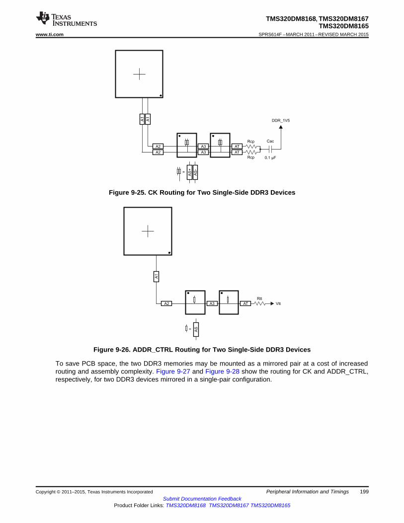
AS=
Rtt
A1
A2 A3 AT Vtt
AS
+
AS
-
=
Rcp
Rcp
Cac
DDR_1V5
0.1 µF
A1
A2 A3 AT
A2 A3 AT
A1
TMS320DM8168, TMS320DM8167TMS320DM8165
www.ti.com SPRS614F –MARCH 2011–REVISED MARCH 2015
Figure 9-25. CK Routing for Two Single-Side DDR3 Devices
Figure 9-26. ADDR_CTRL Routing for Two Single-Side DDR3 Devices
To save PCB space, the two DDR3 memories may be mounted as a mirrored pair at a cost of increasedrouting and assembly complexity. Figure 9-27 and Figure 9-28 show the routing for CK and ADDR_CTRL,respectively, for two DDR3 devices mirrored in a single-pair configuration.
Copyright © 2011–2015, Texas Instruments Incorporated Peripheral Information and Timings 199Submit Documentation Feedback
Product Folder Links: TMS320DM8168 TMS320DM8167 TMS320DM8165

AS=
Rtt
A1
A2 A3 AT Vtt
AS
+
AS
-
=
Rcp
Rcp
Cac
DDR_1V5
0.1 µFA
1
A2 A3 AT
A2 A3 ATA
1
TMS320DM8168, TMS320DM8167TMS320DM8165SPRS614F –MARCH 2011–REVISED MARCH 2015 www.ti.com
Figure 9-27. CK Routing for Two Mirrored DDR3 Devices
Figure 9-28. ADDR_CTRL Routing for Two Mirrored DDR3 Devices
9.3.2.14.3 One DDR3 Device
A single DDR3 device is supported on the DDR EMIF consisting of one x16 DDR3 device arranged asone bank (CS), 16 bits wide.
9.3.2.14.3.1 CK and ADDR_CTRL Topologies, One DDR3 Device
Figure 9-29 shows the topology of the CK net classes and Figure 9-30 shows the topology for thecorresponding ADDR_CTRL net classes.
200 Peripheral Information and Timings Copyright © 2011–2015, Texas Instruments IncorporatedSubmit Documentation Feedback
Product Folder Links: TMS320DM8168 TMS320DM8167 TMS320DM8165

A1 A2
Processor
Address and Control
Output Buffer
DDR Address and Control Input Buffers
AT Vtt
Address and Control
Terminator
Rtt
AS
A1 A2
Processor
Differential Clock
Output Buffer
DDR Differential CK Input Buffer
Routed as Differential Pair
AT
Rcp
Clock Parallel
Terminator
A1 A2 AT
AS
-
AS
+
Rcp
Cac
DDR_1V5
0.1 µF
+
–
+ –
TMS320DM8168, TMS320DM8167TMS320DM8165
www.ti.com SPRS614F –MARCH 2011–REVISED MARCH 2015
Figure 9-29. CK Topology for One DDR3 Device
Figure 9-30. ADDR_CTRL Topology for One DDR3 Device
9.3.2.14.3.2 CK and ADDR_CTRL Routing, One DDR3 Device
Figure 9-31 shows the CK routing for one DDR3 device placed on the same side of the PCB. Figure 9-32shows the corresponding ADDR_CTRL routing.
Copyright © 2011–2015, Texas Instruments Incorporated Peripheral Information and Timings 201Submit Documentation Feedback
Product Folder Links: TMS320DM8168 TMS320DM8167 TMS320DM8165

AS=
Rtt
A1
A2 AT Vtt
AS
+
AS
-
=
Rcp
Rcp
Cac
DDR_1V5
0.1 µF
A1
A2 AT
A2 AT
A1
TMS320DM8168, TMS320DM8167TMS320DM8165SPRS614F –MARCH 2011–REVISED MARCH 2015 www.ti.com
Figure 9-31. CK Routing for One DDR3 Device
Figure 9-32. ADDR_CTRL Routing for One DDR3 Device
9.3.2.15 Data Topologies and Routing Definition
No matter the number of DDR3 devices used, the data line topology is always point to point, so itsdefinition is simple.
9.3.2.15.1 DQS, DQ and DM Topologies, Any Number of Allowed DDR3 Devices
DQS lines are point-to-point differential, and DQ and DM lines are point-to-point singled ended. Figure 9-33 and Figure 9-34 show these topologies.
202 Peripheral Information and Timings Copyright © 2011–2015, Texas Instruments IncorporatedSubmit Documentation Feedback
Product Folder Links: TMS320DM8168 TMS320DM8167 TMS320DM8165
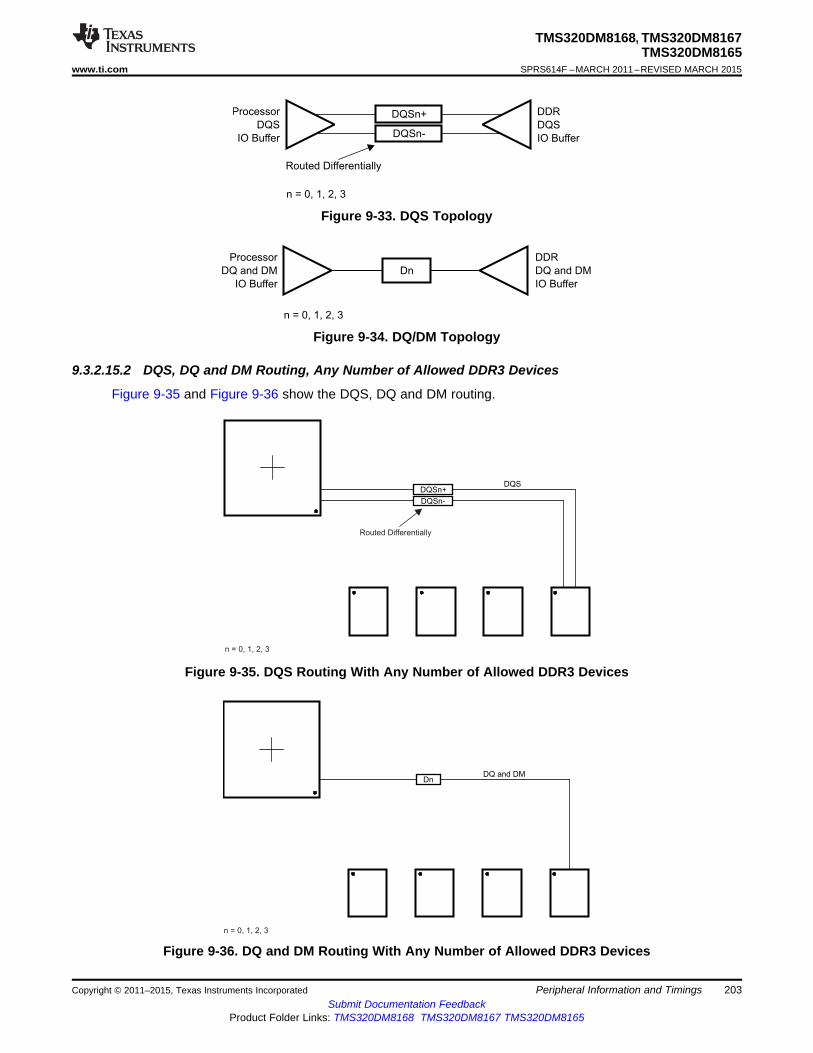
Dn
n = 0, 1, 2, 3
DQ and DM
DQSn+
DQSn-
n = 0, 1, 2, 3
Routed Differentially
DQS
Dn
Processor
DQ and DM
IO Buffer
DDR
DQ and DM
IO Buffer
n = 0, 1, 2, 3
Processor
DQS
IO Buffer
DDR
DQS
IO Buffer
Routed Differentially
n = 0, 1, 2, 3
DQSn-
DQSn+
TMS320DM8168, TMS320DM8167TMS320DM8165
www.ti.com SPRS614F –MARCH 2011–REVISED MARCH 2015
Figure 9-33. DQS Topology
Figure 9-34. DQ/DM Topology
9.3.2.15.2 DQS, DQ and DM Routing, Any Number of Allowed DDR3 Devices
Figure 9-35 and Figure 9-36 show the DQS, DQ and DM routing.
Figure 9-35. DQS Routing With Any Number of Allowed DDR3 Devices
Figure 9-36. DQ and DM Routing With Any Number of Allowed DDR3 Devices
Copyright © 2011–2015, Texas Instruments Incorporated Peripheral Information and Timings 203Submit Documentation Feedback
Product Folder Links: TMS320DM8168 TMS320DM8167 TMS320DM8165

AS=
Rtt
A1
A2 A3 A4 A3 AT Vtt
A8(A)
A8(A)
A8(A)
A8(A)
A8(A)
CACLMX
CACLMY
TMS320DM8168, TMS320DM8167TMS320DM8165SPRS614F –MARCH 2011–REVISED MARCH 2015 www.ti.com
9.3.2.16 Routing Specification
9.3.2.16.1 CK and ADDR_CTRL Routing Specification
Skew within the CK and ADDR_CTRL net classes directly reduces setup and hold margin and, thus, thisskew must be controlled. The only way to practically match lengths on a PCB is to lengthen the shortertraces up to the length of the longest net in the net class and its associated clock. A metric to establishthis maximum length is Manhattan distance. The Manhattan distance between two points on a PCB is thelength between the points when connecting them only with horizontal or vertical segments. A reasonabletrace route length is to within a percentage of its Manhattan distance. CACLM is defined as Clock AddressControl Longest Manhattan distance.
Given the clock and address pin locations on the processor and the DDR3 memories, the maximumpossible Manhattan distance can be determined given the placement. Figure 9-37 and Figure 9-38 showthis distance for four loads and two loads, respectively. It is from this distance that the specifications onthe lengths of the transmission lines for the address bus are determined. CACLM is determined similarlyfor other address bus configurations; that is, it is based on the longest net of the CK and ADDR_CTRL netclass. For CK and ADDR_CTRL routing, these specifications are contained in Table 9-24.
A. It is very likely that the longest CK and ADDR_CTRL Manhattan distance will be for Address Input 8 (A8) on theDDR3 memories. CACLM is based on the longest Manhattan distance due to the device placement. Verify the netclass that satisfies this criteria and use as the baseline for CK and ADDR_CTRL skew matching and length control.
The length of shorter CK and ADDR_CTRL stubs as well as the length of the terminator stub are not included in thislength caculation. Non-included lengths are grayed out in the figure.
Assuming A8 is the longest, CALM = CACLMY + CACLMX + 300 mils.The extra 300 mils allows for routing down lower than the DDR3 memories and returning up to reach A8.
Figure 9-37. CACLM for Four Address Loads on One Side of PCB
204 Peripheral Information and Timings Copyright © 2011–2015, Texas Instruments IncorporatedSubmit Documentation Feedback
Product Folder Links: TMS320DM8168 TMS320DM8167 TMS320DM8165

AS=
Rtt
A1
A2 A3 AT Vtt
A8(A)
A8(A)
A8(A)
CACLMX
CACLMY
TMS320DM8168, TMS320DM8167TMS320DM8165
www.ti.com SPRS614F –MARCH 2011–REVISED MARCH 2015
A. It is very likely that the longest CK and ADDR_CTRL Manhattan distance will be for Address Input 8 (A8) on theDDR3 memories. CACLM is based on the longest Manhattan distance due to the device placement. Verify the netclass that satisfies this criteria and use as the baseline for CK and ADDR_CTRL skew matching and length control.
The length of shorter CK and ADDR_CTRL stubs as well as the length of the terminator stub are not included in thislength caculation. Non-included lengths are grayed out in the figure.
Assuming A8 is the longest, CALM = CACLMY + CACLMX + 300 mils.The extra 300 mils allows for routing down lower than the DDR3 memories and returning up to reach A8.
Figure 9-38. CACLM for Two Address Loads on One Side of PCB
Table 9-24. CK and ADDR_CTRL Routing Specification (1) (2)
NO. PARAMETER MIN TYP MAX UNIT1 A1+A2 length 2500 mils2 A1+A2 skew 25 mils3 A3 length 660 mils4 A3 skew (3) 25 mils5 A3 skew (4) 125 mils6 A4 length 660 mils7 A4 skew 25 mils8 AS length 100 mils9 AS skew 100 mils10 AS+ and AS- length 70 mils11 AS+ and AS- skew 5 mils12 AT length (5) 500 mils13 AT skew (6) 100 mils14 AT skew (7) 5 mils15 CK and ADDR_CTRL nominal trace length (8) CACLM-50 CACLM CACLM+50 mils
(1) The use of vias should be minimized.(2) Additional bypass capacitors are required when using the DDR_1V5 plane as the reference plane to allow the return current to jump
between the DDR_1V5 plane and the ground plane when the net class swtiches layers at a via.(3) Non-mirrored configuration (all DDR3 memories on same side of PCB).(4) Mirrored configuration (one DDR3 device on top of the board and one DDR3 device on the bottom).(5) While this length can be increased for convienience, its length should be minimized.(6) ADDR_CTRL net class only (not CK net class). Minimizing this skew is recommended, but not required.(7) CK net class only.(8) CACLM is the longest Manhattan distance of the CK and ADDR_CTRL net classes + 300 mils. For definition, see Section 9.3.2.16.1,
Figure 9-37, and Figure 9-38.
Copyright © 2011–2015, Texas Instruments Incorporated Peripheral Information and Timings 205Submit Documentation Feedback
Product Folder Links: TMS320DM8168 TMS320DM8167 TMS320DM8165

DQLMX3
DQLMY0
DQLMY3 DQLMY2DB3
DQLMX2
DB2
3 2 1
DQ[23:31]/DM3/DQS3
0
DQ[16:23]/DM2/DQS2
DQLMX1
DB1
DB0
DQLMX0
DQ[8:15]/DM1/DQS1
DQ[0:7]/DM0/DQS0
DQLMY1
DB0 - DB3 represent data bytes 0 - 3.
TMS320DM8168, TMS320DM8167TMS320DM8165SPRS614F –MARCH 2011–REVISED MARCH 2015 www.ti.com
Table 9-24. CK and ADDR_CTRL Routing Specification(1)(2) (continued)NO. PARAMETER MIN TYP MAX UNIT16 Center-to-center CK to other DDR3 trace spacing (9) 4w17 Center-to-center ADDR_CTRL to other DDR3 trace spacing (9) (10) 4w18 Center-to-center ADDR_CTRL to other ADDR_CTRL trace spacing (9) 3w19 CK center-to-center spacing (11)
20 CK spacing to other net (9) 4w21 Rcp (12) Zo-1 Zo Zo+ Ω22 Rtt (12) (13) Zo-5 Zo Zo+5 Ω
(9) Center-to-center spacing is allowed to fall to minimum (w) for up to 1250 mils of routed length.(10) The ADDR_CTRL net class of the other DDR EMIF is considered other DDR3 trace spacing.(11) CK spacing set to ensure proper differential impedance.(12) Source termination (series resistor at driver) is specifically not allowed.(13) Termination values should be uniform across the net class.
9.3.2.16.2 DQS and DQ Routing Specification
Skew within the DQS, DQ and DM net classes directly reduces setup and hold margin and thus this skewmust be controlled. The only way to practically match lengths on a PCB is to lengthen the shorter tracesup to the length of the longest net in the net class and its associated clock. As with CK and ADDR_CTRL,a reasonable trace route length is to within a percentage of its Manhattan distance. DQLMn is defined asDQ Longest Manhattan distance n, where n is the byte number. For a 32-bit interface, there are fourDQLMs, DQLM0-DQLM3. Likewise, for a 16-bit interface, there are two DQLMs, DQLM0-DQLM1.
NOTEIt is not required, nor is it recommended, to match the lengths across all bytes. Lengthmatching is only required within each byte.
Given the DQS, DQ and DM pin locations on the processor and the DDR3 memories, the maximumpossible Manhattan distance can be determined given the placement. Figure 9-39 shows this distance forfour loads. It is from this distance that the specifications on the lengths of the transmission lines for thedata bus are determined. For DQS, DQ and DM routing, these specifications are contained in Table 9-25.
There are four DQLMs, one for each byte (32-bit interface). Each DQLM is the longest Manhattan distance of thebyte; therefore:DQLM0 = DQLMX0 + DQLMY0DQLM1 = DQLMX1 + DQLMY1DQLM2 = DQLMX2 + DQLMY2DQLM3 = DQLMX3 + DQLMY3
Figure 9-39. DQLM for Any Number of Allowed DDR3 Devices
206 Peripheral Information and Timings Copyright © 2011–2015, Texas Instruments IncorporatedSubmit Documentation Feedback
Product Folder Links: TMS320DM8168 TMS320DM8167 TMS320DM8165

TMS320DM8168, TMS320DM8167TMS320DM8165
www.ti.com SPRS614F –MARCH 2011–REVISED MARCH 2015
Table 9-25. Data Routing Specification (1)
NO. PARAMETER MIN TYP MAX UNIT1 DB0 nominal length (2) (3) DQLM0 mils2 DB1 nominal length (2) (4) DQLM1 mils3 DB2 nominal length (2) (5) DQLM2 mils4 DB3 nominal length (2) (6) DQLM3 mils5 DBn skew (7) 25 mils6 DQSn+ to DQSn- skew 5 mils7 DQSn to DBn skew (7) (8) 25 mils8 Center-to-center DBn to other DDR3 trace spacing (9) (10) 4w9 Center-to-center DBn to other DBn trace spacing (9) (11) 3w10 DQSn center-to-center spacing (12)
11 DQSn center-to-center spacing to other net(9) 4w
(1) External termination disallowed. Data termination should use built-in ODT functionality.(2) DQLMn is the longest Manhattan distance of a byte. For definition, see Section 9.3.2.16.2 and Figure 9-39.(3) DQLM0 is the longest Manhattan length for the net classes of Byte 0.(4) DQLM1 is the longest Manhattan length for the net classes of Byte 1.(5) DQLM2 is the longest Manhattan length for the net classes of Byte 2.(6) DQLM3 is the longest Manhattan length for the net slasses of Byte 3.(7) Length matching is only done within a byte. Length matching across bytes is neither required nor recommended.(8) Each DQS pair is length matched to its associated byte.(9) Center-to-center spacing is allowed to fall to minimum (w) for up to 1250 mils of routed length.(10) Other DDR3 trace spacing means other DDR3 net classes not within the byte.(11) This applies to spacing within the net classes of a byte.(12) DQS pair spacing is set to ensure proper differential impedance.
Copyright © 2011–2015, Texas Instruments Incorporated Peripheral Information and Timings 207Submit Documentation Feedback
Product Folder Links: TMS320DM8168 TMS320DM8167 TMS320DM8165

TMS320DM8168, TMS320DM8167TMS320DM8165SPRS614F –MARCH 2011–REVISED MARCH 2015 www.ti.com
9.3.3 DDR2 and DDR3 Memory Controller Register Descriptions
Table 9-26. DDR2 and DDR3 Memory Controller Registers
DDR0 HEX ADDRESS DDR1 HEX ADDRESS ACRONYM REGISTER NAME0x4C00 0004 0x4D00 0004 SDRSTAT SDRAM Status0x4C00 0008 0x4D00 0008 SDRCR SDRAM Config0x4C00 000C 0x4D00 000C SDRCR2 SDRAM Config 20x4C00 0010 0x4D00 0010 SDRRCR SDRAM Refresh Control0x4C00 0014 0x4D00 0014 SDRRCSR SDRAM Refresh Control Shadow0x4C00 0018 0x4D00 0018 SDRTIM1 SDRAM Timing 10x4C00 001C 0x4D00 001C SDRTIM1SR SDRAM Timing 1 Shadow0x4C00 0020 0x4D00 0020 SDRTIM2 SDRAM Timing 20x4C00 0024 0x4D00 0024 SDRTIM2SR SDRAM Timing 2 Shadow0x4C00 0028 0x4D00 0028 SDRTIM3 SDRAM Timing 30x4C00 002C 0x4D00 002C SDRTIM3SR SDRAM Timing 3 Shadow0x4C00 0038 0x4D00 0038 PMCR Power Management Control0x4C00 003C 0x4D00 003C PMCSR Power Management Control Shadow0x4C00 0054 0x4D00 0054 PBBPR Peripheral Bus Burst Priority0x4C00 00A0 0x4D00 00A0 EOI End of Interrupt0x4C00 00A4 0x4D00 00A4 SOIRSR System OCP Interrupt Raw Status0x4C00 00AC 0x4D00 00AC SOISR System OCP Interrupt Status0x4C00 00B4 0x4D00 00B4 SOIESR System OCP Interrupt Enable Set0x4C00 00BC 0x4D00 00BC SOIECR System OCP Interrupt Enable Clear0x4C00 00C8 0x4D00 00C8 ZQCR SDRAM output Impedance Calibration Config0x4C00 00DC 0x4D00 00DC RWLCR Read-Write Leveling Control0x4C00 00E4 0x4D00 00E4 DDRPHYCR DDR PHY Control0x4C00 00E8 0x4D00 00E8 DDRPHYCSR DDR PHY Control Shadow
9.3.4 DDR2 and DDR3 PHY Register Descriptions
Table 9-27. DDR2 and DDR3 PHY Registers
DDR0 HEX DDR1 HEX ACRONYM REGISTER NAMEADDRESS ADDRESS0x4819 800C 0x4819 A00C CMD0_IO_CONFIG_I_0 Command 0 Address and Command Pad
Configuration0x4819 8010 0x4819 A010 CMD0_IO_CONFIG_I_CLK_0 Command 0 Clock Pad Configuration0x4819 8014 0x4819 A014 CMD0_IO_CONFIG_SR_0 Command 0 Address and Command Slew
Rate Configuration0x4819 8018 0x4819 A018 CMD0_IO_CONFIG_SR_CLK_0 Command 0 Clock Pad Slew Rate
Configuration0x4819 801C 0x4819 A01C CMD0_REG_PHY_CTRL_SLAVE_RATIO_0 Command 0 Address and Command Slave
Ratio0x4819 802C 0x4819 A02C CMD0_REG_PHY_INVERT_CLKOUT_0 Command 0 Invert Clockout Selection0x4819 8040 0x4819 A040 CMD1_IO_CONFIG_I_0 Command 1 Address and Command Pad
Configuration0x4819 8044 0x4819 A044 CMD1_IO_CONFIG_I_CLK_0 Command 1 Clock Pad Configuration0x4819 8048 0x4819 A048 CMD1_IO_CONFIG_SR_0 Command 1 Address and Command Slew
Rate Configuration0x4819 804C 0x4819 A04C CMD1_IO_CONFIG_SR_CLK_0 Command 1 Clock Pad Slew Rate
Configuration0x4819 8050 0x4819 A050 CMD1_REG_PHY_CTRL_SLAVE_RATIO_0 Command 1 Address and Command Slave
Ratio
208 Peripheral Information and Timings Copyright © 2011–2015, Texas Instruments IncorporatedSubmit Documentation Feedback
Product Folder Links: TMS320DM8168 TMS320DM8167 TMS320DM8165

TMS320DM8168, TMS320DM8167TMS320DM8165
www.ti.com SPRS614F –MARCH 2011–REVISED MARCH 2015
Table 9-27. DDR2 and DDR3 PHY Registers (continued)DDR0 HEX DDR1 HEX ACRONYM REGISTER NAMEADDRESS ADDRESS
0x4819 8060 0x4819 A060 CMD1_REG_PHY_INVERT_CLKOUT_0 Command 1 Invert Clockout Selection0x4819 8074 0x4819 A074 CMD2_IO_CONFIG_I_0 Command 2 Address and Command Pad
Configuration0x4819 8078 0x4819 A078 CMD2_IO_CONFIG_I_CLK_0 Command 2 Clock Pad Configuration0x4819 807C 0x4819 A07C CMD2_IO_CONFIG_SR_0 Command 2 Address and Command Slew
Rate Configuration0x4819 8080 0x4819 A080 CMD2_IO_CONFIG_SR_CLK_0 Command 2 Clock Pad Slew Rate
Configuration0x4819 8084 0x4819 A084 CMD2_REG_PHY_CTRL_SLAVE_RATIO_0 Command 2 Address and Command Slave
Ratio0x4819 8094 0x4819 A094 CMD2_REG_PHY_INVERT_CLKOUT_0 Command 2 Invert Clockout Selection0x4819 80A8 0x4819 A0A8 DATA0_IO_CONFIG_I_0 Data Macro 0 Data Pad Configuration0x4819 80AC 0x4819 A0AC DATA0_IO_CONFIG_I_CLK_0 Data Macro 0 Data Strobe Pad Configuration0x4819 80B0 0x4819 A0B0 DATA0_IO_CONFIG_SR_0 Data Macro 0 Data Slew Rate Configuration0x4819 80B4 0x4819 A0B4 DATA0_IO_CONFIG_SR_CLK_0 Data Macro 0 Data Strobe Slew Rate
Configuration0x4819 80C8 0x4819 A0C8 DATA0_REG_PHY_RD_DQS_SLAVE_RATIO_0 Data Macro 0 Read DQS Slave Ratio0x4819 80DC 0x4819 A0DC DATA0_REG_PHY_WR_DQS_SLAVE_RATIO_0 Data Macro 0 Write DQS Slave Ratio0x4819 80F0 0x4819 A0F0 DATA0_REG_PHY_WRLVL_INIT_RATIO_0 Data Macro 0 Write Leveling Init Ratio0x4819 80F8 0x4819 A0F8 DATA0_REG_PHY_WRLVL_INIT_MODE_0 Data Macro 0 Write Leveling Init Mode Ratio
Selection0x4819 80FC 0x4819 A0FC DATA0_REG_PHY_GATELVL_INIT_RATIO_0 Data Macro 0 DQS Gate Training Init Ratio0x4819 8104 0x4819 A104 DATA0_REG_PHY_GATELVL_INIT_MODE_0 Data Macro 0 DQS Gate Training Init Mode
Ratio Selection0x4819 8108 0x4819 A108 DATA0_REG_PHY_FIFO_WE_SLAVE_RATIO_0 Data Macro 0 DQS Gate Slave Ratio0x4819 8120 0x4819 A120 DATA0_REG_PHY_WR_DATA_SLAVE_RATIO_0 Data Macro 0 Write Data Slave Ratio0x4819 8134 0x4819 A134 DATA0_REG_PHY_USE_RANK0_DELAYS Data Macro 0 Delay Selection0x4819 814C 0x4819 A14C DATA1_IO_CONFIG_I_0 Data Macro 1 Data Pad Configuration0x4819 8150 0x4819 A150 DATA1_IO_CONFIG_I_CLK_0 Data Macro 1 Data Strobe Pad Configuration0x4819 8154 0x4819 A154 DATA1_IO_CONFIG_SR_0 Data Macro 1 Data Slew Rate Configuration0x4819 8158 0x4819 A158 DATA1_IO_CONFIG_SR_CLK_0 Data Macro 1 Data Strobe Slew Rate
Configuration0x4819 816C 0x4819 A16C DATA1_REG_PHY_RD_DQS_SLAVE_RATIO_0 Data Macro 1 Read DQS Slave Ratio0x4819 8180 0x4819 A180 DATA1_REG_PHY_WR_DQS_SLAVE_RATIO_0 Data Macro 1 Write DQS Slave Ratio0x4819 8194 0x4819 A194 DATA1_REG_PHY_WRLVL_INIT_RATIO_0 Data Macro 1 Write Leveling Init Ratio0x4819 819C 0x4819 A19C DATA1_REG_PHY_WRLVL_INIT_MODE_0 Data Macro 1 Write Leveling Init Mode Ratio
Selection0x4819 81A0 0x4819 A1A0 DATA1_REG_PHY_GATELVL_INIT_RATIO_0 Data Macro 1 DQS Gate Training Init Ratio0x4819 81A8 0x4819 A1A8 DATA1_REG_PHY_GATELVL_INIT_MODE_0 Data Macro 1 DQS Gate Training Init Mode
Ratio Selection0x4819 81AC 0x4819 A1AC DATA1_REG_PHY_FIFO_WE_SLAVE_RATIO_0 Data Macro 1 DQS Gate Slave Ratio0x4819 81C4 0x4819 A1C4 DATA1_REG_PHY_WR_DATA_SLAVE_RATIO_0 Data Macro 1 Write Data Slave Ratio0x4819 81D8 0x4819 A1D8 DATA1_REG_PHY_USE_RANK0_DELAYS Data Macro 1 Delay Selection0x4819 81F0 0x4819 A1F0 DATA2_IO_CONFIG_I_0 Data Macro 2 Data Pad Configuration0x4819 81F4 0x4819 A1F4 DATA2_IO_CONFIG_I_CLK_0 Data Macro 2 Data Strobe Pad Configuration0x4819 81F8 0x4819 A1F8 DATA2_IO_CONFIG_SR_0 Data Macro 2 Data Slew Rate Configuration0x4819 81FC 0x4819 A1FC DATA2_IO_CONFIG_SR_CLK_0 Data Macro 2 Data Strobe Slew Rate
Configuration0x4819 8210 0x4819 A210 DATA2_REG_PHY_RD_DQS_SLAVE_RATIO_0 Data Macro 2 Read DQS Slave Ratio0x4819 8224 0x4819 A224 DATA2_REG_PHY_WR_DQS_SLAVE_RATIO_0 Data Macro 2 Write DQS Slave Ratio
Copyright © 2011–2015, Texas Instruments Incorporated Peripheral Information and Timings 209Submit Documentation Feedback
Product Folder Links: TMS320DM8168 TMS320DM8167 TMS320DM8165

TMS320DM8168, TMS320DM8167TMS320DM8165SPRS614F –MARCH 2011–REVISED MARCH 2015 www.ti.com
Table 9-27. DDR2 and DDR3 PHY Registers (continued)DDR0 HEX DDR1 HEX ACRONYM REGISTER NAMEADDRESS ADDRESS
0x4819 8238 0x4819 A238 DATA2_REG_PHY_WRLVL_INIT_RATIO_0 Data Macro 2 Write Leveling Init Ratio0x4819 8240 0x4819 A240 DATA2_REG_PHY_WRLVL_INIT_MODE_0 Data Macro 2 Write Leveling Init Mode Ratio
Selection0x4819 8244 0x4819 A244 DATA2_REG_PHY_GATELVL_INIT_RATIO_0 Data Macro 2 DQS Gate Training Init Ratio0x4819 824C 0x4819 A24C DATA2_REG_PHY_GATELVL_INIT_MODE_0 Data Macro 2 DQS Gate Training Init Mode
Ratio Selection0x4819 8250 0x4819 A250 DATA2_REG_PHY_FIFO_WE_SLAVE_RATIO_0 Data Macro 2 DQS Gate Slave Ratio0x4819 8268 0x4819 A268 DATA2_REG_PHY_WR_DATA_SLAVE_RATIO_0 Data Macro 2 Write Data Slave Ratio0x4819 827C 0x4819 A27C DATA2_REG_PHY_USE_RANK0_DELAYS Data Macro 2 Delay Selection0x4819 8294 0x4819 A294 DATA3_IO_CONFIG_I_0 Data Macro 3 Data Pad Configuration0x4819 8298 0x4819 A298 DATA3_IO_CONFIG_I_CLK_0 Data Macro 3 Data Strobe Pad Configuration0x4819 829C 0x4819 A29C DATA3_IO_CONFIG_SR_0 Data Macro 3 Data Slew Rate Configuration0x4819 82A0 0x4819 A2A0 DATA3_IO_CONFIG_SR_CLK_0 Data Macro 3 Data Strobe Slew Rate
Configuration0x4819 82B4 0x4819 A2B4 DATA3_REG_PHY_RD_DQS_SLAVE_RATIO_0 Data Macro 3 Read DQS Slave Ratio0x4819 82C8 0x4819 A2C8 DATA3_REG_PHY_WR_DQS_SLAVE_RATIO_0 Data Macro 3 Write DQS Slave Ratio0x4819 82DC 0x4819 A2DC DATA3_REG_PHY_WRLVL_INIT_RATIO_0 Data Macro 3 Write Leveling Init Ratio0x4819 82E4 0x4819 A2E4 DATA3_REG_PHY_WRLVL_INIT_MODE_0 Data Macro 3 Write Leveling Init Mode Ratio
Selection0x4819 82E8 0x4819 A2E8 DATA3_REG_PHY_GATELVL_INIT_RATIO_0 Data Macro 3 DQS Gate Training Init Ratio0x4819 82F0 0x4819 A2F0 DATA3_REG_PHY_GATELVL_INIT_MODE_0 Data Macro 3 DQS Gate Training Init Mode
Ratio Selection0x4819 82F4 0x4819 A2F4 DATA3_REG_PHY_FIFO_WE_SLAVE_RATIO_0 Data Macro 3 DQS Gate Slave Ratio0x4819 830C 0x4819 A30C DATA3_REG_PHY_WR_DATA_SLAVE_RATIO_0 Data Macro 3 Write Data Slave Ratio0x4819 8320 0x4819 A320 DATA3_REG_PHY_USE_RANK0_DELAYS Data Macro 3 Delay Selection0x4819 8358 0x4819 A358 DDR_VTP_CTRL_0 DDR VTP Control
9.3.5 DDR2 and DDR3 Memory Controller Electrical Data and TimingSection 9.3.1, DDR2 Routing Specifications and Section 9.3.2, DDR3 Routing Specifications specify acomplete DDR2 and DDR3 interface solution for the device. TI has performed the simulation and systemcharacterization to ensure all DDR2 and DDR3 interface timings in this solution are met.
TI only supports board designs that follow the specifications outlined in the DDR2 Routing Specificationsand DDR3 Routing Specifications sections of this data sheet.
210 Peripheral Information and Timings Copyright © 2011–2015, Texas Instruments IncorporatedSubmit Documentation Feedback
Product Folder Links: TMS320DM8168 TMS320DM8167 TMS320DM8165

TMS320DM8168, TMS320DM8167TMS320DM8165
www.ti.com SPRS614F –MARCH 2011–REVISED MARCH 2015
9.4 Emulation Features and Capability
9.4.1 Advanced Event Triggering (AET)The device supports Advanced Event Triggering (AET). This capability can be used to debug complexproblems as well as understand performance characteristics of user applications. AET provides thefollowing capabilities:• Hardware Program Breakpoints: specify addresses or address ranges that can generate events such
as halting the processor or triggering the trace capture.• Data Watchpoints: specify data variable addresses, address ranges, or data values that can generate
events such as halting the processor or triggering the trace capture.• Counters: count the occurrence of an event or cycles for performance monitoring.• State Sequencing: allows combinations of hardware program breakpoints and data watchpoints to
precisely generate events for complex sequences.
For more information on AET, see the following documents:• Using Advanced Event Triggering to Find and Fix Intermittent Real-Time Bugs application report
(literature number SPRA753)• Using Advanced Event Triggering to Debug Real-Time Problems in High Speed Embedded
Microprocessor Systems application report (literature number SPRA387)
9.4.2 TraceThe device supports Trace at the Cortex™-A8, C674x, and System levels. Trace is a debug technologythat provides a detailed, historical account of application code execution, timing, and data accesses. Tracecollects, compresses, and exports debug information for analysis. The debug information can be exportedto the Embedded Trace Buffer (ETB), or to the 5-pin Trace Interface (system trace only). Trace works inreal-time and does not impact the execution of the system.
For more information on board design guidelines for Trace Advanced Emulation, see the Emulation andTrace Headers Technical Reference Manual (literature number SPRU655).
9.4.3 IEEE 1149.1 JTAGThe JTAG (IEEE Standard 1149.1-1990 Standard-Test-Access Port and Boundary Scan Architecture)interface is used for BSDL testing and emulation of the device. The TRST pin only needs to be releasedwhen it is necessary to use a JTAG controller to debug the device or exercise the device's boundary scanfunctionality. For maximum reliability, the device includes an internal pulldown (IPD) on the TRST pin toensure that TRST is always asserted upon power up and the device's internal emulation logic is alwaysproperly initialized. JTAG controllers from Texas Instruments actively drive TRST high. However, somethird-party JTAG controllers may not drive TRST high but expect the use of a pullup resistor on TRST.When using this type of JTAG controller, assert TRST to initialize the device after powerup and externallydrive TRST high before attempting any emulation or boundary-scan operations.
The main JTAG features include:• 32KB embedded trace buffer (ETB)• 5-pin system trace interface for debug• Supports Advanced Event Triggering (AET)• All processors can be emulated via JTAG ports• All functions on EMU pins of the device:
– EMU[1:0] - cross-triggering, boot mode (WIR), STM trace– EMU[4:2] - STM trace only (single direction)– EMU[2] - only valid pin to use as clock
Copyright © 2011–2015, Texas Instruments Incorporated Peripheral Information and Timings 211Submit Documentation Feedback
Product Folder Links: TMS320DM8168 TMS320DM8167 TMS320DM8165
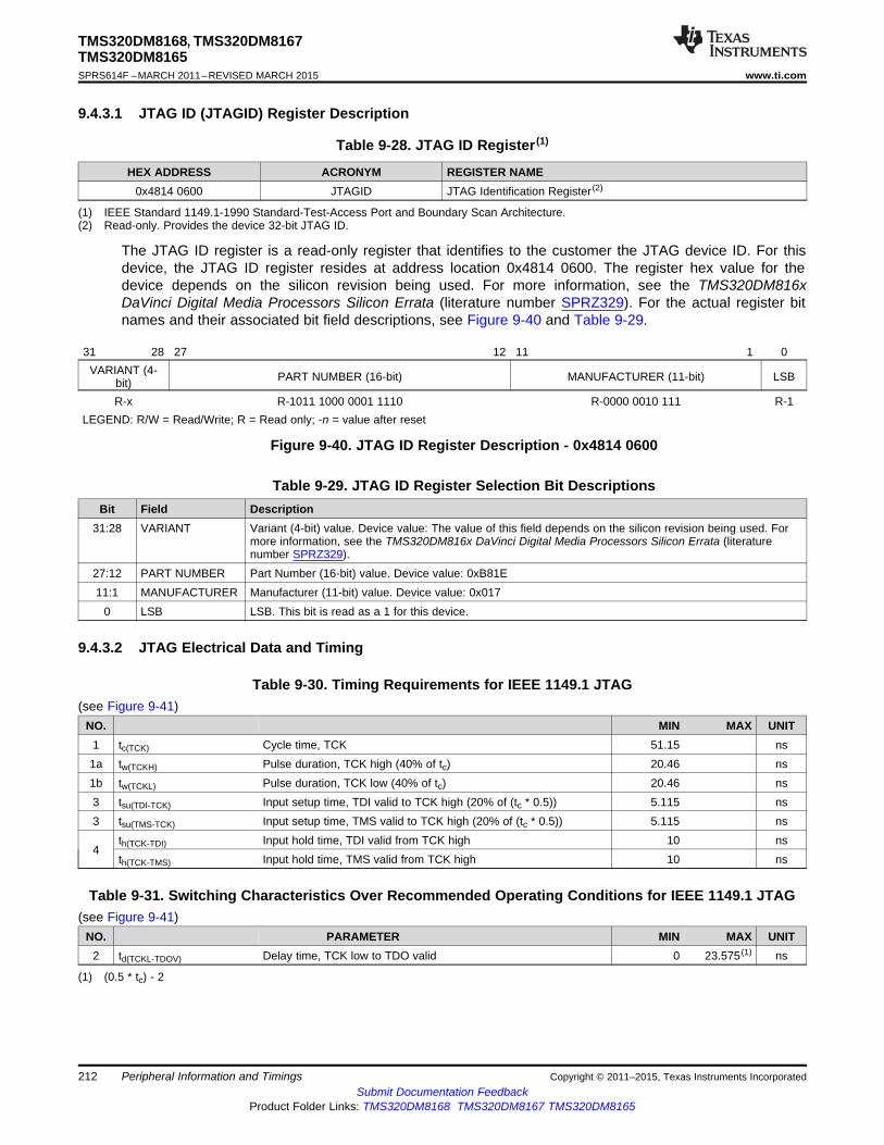
TMS320DM8168, TMS320DM8167TMS320DM8165SPRS614F –MARCH 2011–REVISED MARCH 2015 www.ti.com
9.4.3.1 JTAG ID (JTAGID) Register Description
Table 9-28. JTAG ID Register (1)
HEX ADDRESS ACRONYM REGISTER NAME0x4814 0600 JTAGID JTAG Identification Register (2)
(1) IEEE Standard 1149.1-1990 Standard-Test-Access Port and Boundary Scan Architecture.(2) Read-only. Provides the device 32-bit JTAG ID.
The JTAG ID register is a read-only register that identifies to the customer the JTAG device ID. For thisdevice, the JTAG ID register resides at address location 0x4814 0600. The register hex value for thedevice depends on the silicon revision being used. For more information, see the TMS320DM816xDaVinci Digital Media Processors Silicon Errata (literature number SPRZ329). For the actual register bitnames and their associated bit field descriptions, see Figure 9-40 and Table 9-29.
31 28 27 12 11 1 0VARIANT (4- PART NUMBER (16-bit) MANUFACTURER (11-bit) LSBbit)
R-x R-1011 1000 0001 1110 R-0000 0010 111 R-1LEGEND: R/W = Read/Write; R = Read only; -n = value after reset
Figure 9-40. JTAG ID Register Description - 0x4814 0600
Table 9-29. JTAG ID Register Selection Bit DescriptionsBit Field Description
31:28 VARIANT Variant (4-bit) value. Device value: The value of this field depends on the silicon revision being used. Formore information, see the TMS320DM816x DaVinci Digital Media Processors Silicon Errata (literaturenumber SPRZ329).
27:12 PART NUMBER Part Number (16-bit) value. Device value: 0xB81E11:1 MANUFACTURER Manufacturer (11-bit) value. Device value: 0x017
0 LSB LSB. This bit is read as a 1 for this device.
9.4.3.2 JTAG Electrical Data and Timing
Table 9-30. Timing Requirements for IEEE 1149.1 JTAG(see Figure 9-41)
NO. MIN MAX UNIT1 tc(TCK) Cycle time, TCK 51.15 ns1a tw(TCKH) Pulse duration, TCK high (40% of tc) 20.46 ns1b tw(TCKL) Pulse duration, TCK low (40% of tc) 20.46 ns3 tsu(TDI-TCK) Input setup time, TDI valid to TCK high (20% of (tc * 0.5)) 5.115 ns3 tsu(TMS-TCK) Input setup time, TMS valid to TCK high (20% of (tc * 0.5)) 5.115 ns
th(TCK-TDI) Input hold time, TDI valid from TCK high 10 ns4
th(TCK-TMS) Input hold time, TMS valid from TCK high 10 ns
Table 9-31. Switching Characteristics Over Recommended Operating Conditions for IEEE 1149.1 JTAG(see Figure 9-41)
NO. PARAMETER MIN MAX UNIT2 td(TCKL-TDOV) Delay time, TCK low to TDO valid 0 23.575 (1) ns
(1) (0.5 * tc) - 2
212 Peripheral Information and Timings Copyright © 2011–2015, Texas Instruments IncorporatedSubmit Documentation Feedback
Product Folder Links: TMS320DM8168 TMS320DM8167 TMS320DM8165

5
6
87
TCK
RTCK
3
TCK
TDO
TDI/TMS
2
4
1
1a 1b
TMS320DM8168, TMS320DM8167TMS320DM8165
www.ti.com SPRS614F –MARCH 2011–REVISED MARCH 2015
Figure 9-41. JTAG Timing
Table 9-32. Timing Requirements for IEEE 1149.1 JTAG With RTCK(see Figure 9-41)
NO. MIN MAX UNIT1 tc(TCK) Cycle time, TCK 51.15 ns1a tw(TCKH) Pulse duration, TCK high (40% of tc) 20.46 ns1b tw(TCKL) Pulse duration, TCK low (40% of tc) 20.46 ns3 tsu(TDI-TCK) Input setup time, TDI valid to TCK high (20% of (tc * 0.5)) 5.115 ns3 tsu(TMS-TCK) Input setup time, TMS valid to TCK high (20% of (tc * 0.5)) 5.115 ns
th(TCK-TDI) Input hold time, TDI valid from TCK high 10 ns4
th(TCK-TMS) Input hold time, TMS valid from TCK high 10 ns
Table 9-33. Switching Characteristics Over Recommended Operating Conditions for IEEE 1149.1 JTAGWith RTCK
(see Figure 9-42)NO. PARAMETER MIN MAX UNIT
Delay time, TCK to RTCK with no selected subpaths (that is,ICEPick module is the only tap selected - when the ARM is in the5 td(TCK-RTCK) 0 21 nsscan chain, the delay time is a function of the ARM functionalclock.)
6 tc(RTCK) Cycle time, RTCK 51.15 ns7 tw(RTCKH) Pulse duration, RTCK high (40% of tc) 20.46 ns8 tw(RTCKL) Pulse duration, RTCK low (40% of tc) 20.46 ns
Figure 9-42. JTAG With RTCK Timing
Copyright © 2011–2015, Texas Instruments Incorporated Peripheral Information and Timings 213Submit Documentation Feedback
Product Folder Links: TMS320DM8168 TMS320DM8167 TMS320DM8165

TMS320DM8168, TMS320DM8167TMS320DM8165SPRS614F –MARCH 2011–REVISED MARCH 2015 www.ti.com
9.4.4 IEEE 1149.7 cJTAGBesides the standard (legacy) JTAG mode of operation, the target debug interface can also be switched toa compressed JTAG (cJTAG) mode of operation, commonly referred to as IEEE1149.7 standard. AnIEEE1149.7 adapter module runs a 2-pin communication protocol on top of an IEEE1149.1 JTAG TAP.The debug-IP logic serializes the IEEE1149.1 transactions, using a variety of compression formats, toreduce the number of pins needed to implement a JTAG debug port. This device implements only asubset of the IEEE1149.7 protocol; it supports Class 0 and Class 1 operation. On this device the cJTAGID[7:0] is tied to 0x00.
NOTEThe default setting of the scan port is IEEE 1149.1. A cJTAG emulator connected only toTCLK and TMS can re-configure the port to cJTAG by scanning in a special commandsequence. For the scan sequence required to switch modes, see the IEEE1149.7specification.
214 Peripheral Information and Timings Copyright © 2011–2015, Texas Instruments IncorporatedSubmit Documentation Feedback
Product Folder Links: TMS320DM8168 TMS320DM8167 TMS320DM8165

TMS320DM8168, TMS320DM8167TMS320DM8165
www.ti.com SPRS614F –MARCH 2011–REVISED MARCH 2015
9.5 Enhanced Direct Memory Access (EDMA) ControllerThe EDMA controller handles all data transfers between memories and the device slave peripherals onthe device. These data transfers include cache servicing, non-cacheable memory accesses, user-programmed data transfers, and host accesses.
9.5.1 EDMA Channel Synchronization EventsThe EDMA channel controller supports up to 64 channels that service peripherals and memory. EachEDMA channel is mapped to a default EDMA synchronization event as shown in Table 9-34. By default,each event uses the parameter entry that matches its event number. However, because the deviceincludes a channel mapping feature, each event may be mapped to any of 512 parameter table entries.For more detailed information on the EDMA module and how EDMA events are enabled, captured,processed, linked, chained, and cleared, see the EDMA chapter in the TMS320DM816x DaVinci DigitalMedia Processors Technical Reference Manual (literature number SPRUGX8).
Table 9-34. EDMA Default Synchronization Events
EVENT NUMBER DEFAULT EVENT NAME DEFAULT EVENT DESCRIPTION0 - 7 - Unused
8 AXEVT0 McASP0 Transmit9 AREVT0 McASP0 Receive10 AXEVT1 McASP1 Transmit11 AREVT1 McASP1 Receive12 AXEVT2 McASP2 Transmit13 AREVT2 McASP2 Receive14 BXEVT McBSP Transmit15 BREVT McBSP Receive16 SPIXEVT0 SPI0 Transmit 017 SPIREVT0 SPI0 Receive 018 SPIXEVT1 SPI0 Transmit 119 SPIREVT1 SPI0 Receive 120 SPIXEVT2 SPI0 Transmit 221 SPIREVT2 SPI0 Receive 222 SPIXEVT3 SPI0 Transmit 323 SPIREVT3 SPI0 Receive 324 SDTXEVT SD0 Transmit25 SDRXEVT SD0 Receive26 UTXEVT0 UART0 Transmit27 URXEVT0 UART0 Receive28 UTXEVT1 UART1 Transmit29 URXEVT1 UART1 Receive30 UTXEVT2 UART2 Transmit31 URXEVT2 UART2 Receive
32 - 47 - Unused48 TINT4 TIMER449 TINT5 TIMER550 TINT6 TIMER651 TINT7 TIMER752 GPMCEVT GPMC53 HDMIEVT HDMI
54 - 57 - Unused58 I2CTXEVT0 I2C0 Transmit
Copyright © 2011–2015, Texas Instruments Incorporated Peripheral Information and Timings 215Submit Documentation Feedback
Product Folder Links: TMS320DM8168 TMS320DM8167 TMS320DM8165
TMS320DM8168, TMS320DM8167TMS320DM8165SPRS614F –MARCH 2011–REVISED MARCH 2015 www.ti.com
Table 9-34. EDMA Default Synchronization Events (continued)EVENT NUMBER DEFAULT EVENT NAME DEFAULT EVENT DESCRIPTION
59 I2CRXEVT0 I2C0 Receive60 I2CTXEVT1 I2C1 Transmit61 I2CRXEVT1 I2C1 Receive
62 - 63 - Unused
9.5.2 EDMA Peripheral Register Descriptions
Table 9-35. EDMA Channel Controller (EDMA TPCC) Control Registers
HEX ADDRESS ACRONYM REGISTER NAME0x4900 0000 PID Peripheral Identification0x4900 0004 CCCFG EDMA3CC Configuration
0x4900 0100 - 0x4900 01FC DCHMAP0-63 DMA Channel 0-63 Mappings0x4900 0200 QCHMAP0 QDMA Channel 0 Mapping0x4900 0204 QCHMAP1 QDMA Channel 1 Mapping0x4900 0208 QCHMAP2 QDMA Channel 2 Mapping0x4900 020C QCHMAP3 QDMA Channel 3 Mapping0x4900 0210 QCHMAP4 QDMA Channel 4 Mapping0x4900 0214 QCHMAP5 QDMA Channel 5 Mapping0x4900 0218 QCHMAP6 QDMA Channel 6 Mapping0x4900 021C QCHMAP7 QDMA Channel 7 Mapping0x4900 0240 DMAQNUM0 DMA Queue Number 00x4900 0244 DMAQNUM1 DMA Queue Number 10x4900 0248 DMAQNUM2 DMA Queue Number 20x4900 024C DMAQNUM3 DMA Queue Number 30x4900 0250 DMAQNUM4 DMA Queue Number 40x4900 0254 DMAQNUM5 DMA Queue Number 50x4900 0258 DMAQNUM6 DMA Queue Number 60x4900 025C DMAQNUM7 DMA Queue Number 70x4900 0260 QDMAQNUM QDMA Queue Number0x4900 0284 QUEPRI Queue Priority0x4900 0300 EMR Event Missed0x4900 0304 EMRH Event Missed High0x4900 0308 EMCR Event Missed Clear0x4900 030C EMCRH Event Missed Clear High0x4900 0310 QEMR QDMA Event Missed0x4900 0314 QEMCR QDMA Event Missed Clear0x4900 0318 CCERR EDMA3CC Error0x4900 031C CCERRCLR EDMA3CC Error Clear0x4900 0320 EEVAL Error Evaluate0x4900 0340 DRAE0 DMA Region Access Enable for Region 00x4900 0344 DRAEH0 DMA Region Access Enable High for Region 00x4900 0348 DRAE1 DMA Region Access Enable for Region 10x4900 034C DRAEH1 DMA Region Access Enable High for Region 10x4900 0350 DRAE2 DMA Region Access Enable for Region 20x4900 0354 DRAEH2 DMA Region Access Enable High for Region 20x4900 0358 DRAE3 DMA Region Access Enable for Region 30x4900 035C DRAEH3 DMA Region Access Enable High for Region 3
216 Peripheral Information and Timings Copyright © 2011–2015, Texas Instruments IncorporatedSubmit Documentation Feedback
Product Folder Links: TMS320DM8168 TMS320DM8167 TMS320DM8165
TMS320DM8168, TMS320DM8167TMS320DM8165
www.ti.com SPRS614F –MARCH 2011–REVISED MARCH 2015
Table 9-35. EDMA Channel Controller (EDMA TPCC) Control Registers (continued)HEX ADDRESS ACRONYM REGISTER NAME
0x4900 0360 DRAE4 DMA Region Access Enable for Region 40x4900 0364 DRAEH4 DMA Region Access Enable High for Region 40x4900 0368 DRAE5 DMA Region Access Enable for Region 50x4900 036C DRAEH5 DMA Region Access Enable High for Region 50x4900 0370 DRAE6 DMA Region Access Enable for Region 60x4900 0374 DRAEH6 DMA Region Access Enable High for Region 60x4900 0378 DRAE7 DMA Region Access Enable for Region 70x4900 037C DRAEH7 DMA Region Access Enable High for Region 7
0x4900 0380 - 0x4900 039C QRAE0-7 QDMA Region Access Enable for Region 0-70x4900 0400 - 0x4900 04FC Q0E0-Q3E15 Event Queue Entry Q0E0-Q3E150x4900 0600 - 0x4900 060C QSTAT0-3 Queue Status 0-3
0x4900 0620 QWMTHRA Queue Watermark Threshold A0x4900 0640 CCSTAT EDMA3CC Status0x4900 0800 MPFAR Memory Protection Fault Address0x4900 0804 MPFSR Memory Protection Fault Status0x4900 0808 MPFCR Memory Protection Fault Command0x4900 080C MPPAG Memory Protection Page Attribute Global
0x4900 0810 - 0x4900 082C MPPA0-7 Memory Protection Page Attribute 0-70x4900 1000 ER Event0x4900 1004 ERH Event High0x4900 1008 ECR Event Clear0x4900 100C ECRH Event Clear High0x4900 1010 ESR Event Set0x4900 1014 ESRH Event Set High0x4900 1018 CER Chained Event0x4900 101C CERH Chained Event High0x4900 1020 EER Event Enable0x4900 1024 EERH Event Enable High0x4900 1028 EECR Event Enable Clear0x4900 102C EECRH Event Enable Clear High0x4900 1030 EESR Event Enable Set0x4900 1034 EESRH Event Enable Set High0x4900 1038 SER Secondary Event0x4900 103C SERH Secondary Event High0x4900 1040 SECR Secondary Event Clear0x4900 1044 SECRH Secondary Event Clear High0x4900 1050 IER Interrupt Enable0x4900 1054 IERH Interrupt Enable High0x4900 1058 IECR Interrupt Enable Clear0x4900 105C IECRH Interrupt Enable Clear High0x4900 1060 IESR Interrupt Enable Set0x4900 1064 IESRH Interrupt Enable Set High0x4900 1068 IPR Interrupt Pending0x4900 106C IPRH Interrupt Pending High0x4900 1070 ICR Interrupt Clear0x4900 1074 ICRH Interrupt Clear High0x4900 1078 IEVAL Interrupt Evaluate
Copyright © 2011–2015, Texas Instruments Incorporated Peripheral Information and Timings 217Submit Documentation Feedback
Product Folder Links: TMS320DM8168 TMS320DM8167 TMS320DM8165
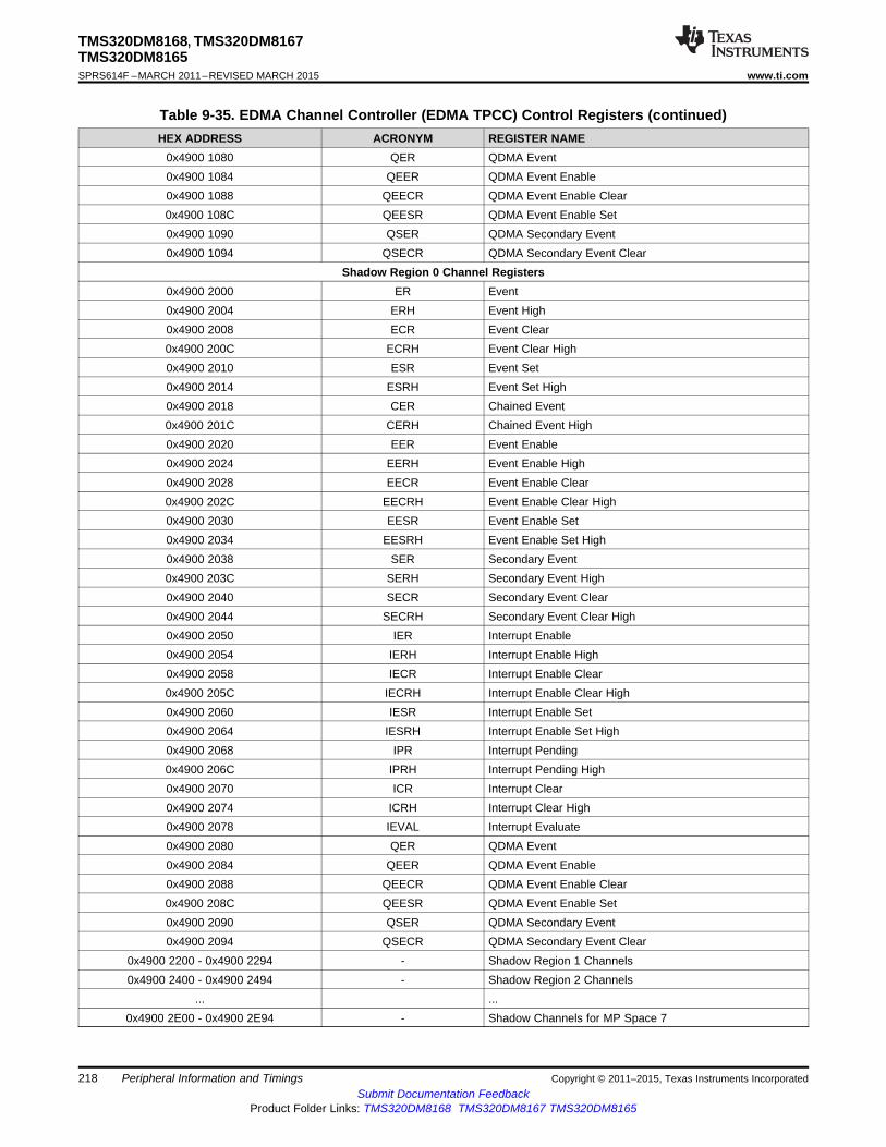
TMS320DM8168, TMS320DM8167TMS320DM8165SPRS614F –MARCH 2011–REVISED MARCH 2015 www.ti.com
Table 9-35. EDMA Channel Controller (EDMA TPCC) Control Registers (continued)HEX ADDRESS ACRONYM REGISTER NAME
0x4900 1080 QER QDMA Event0x4900 1084 QEER QDMA Event Enable0x4900 1088 QEECR QDMA Event Enable Clear0x4900 108C QEESR QDMA Event Enable Set0x4900 1090 QSER QDMA Secondary Event0x4900 1094 QSECR QDMA Secondary Event Clear
Shadow Region 0 Channel Registers0x4900 2000 ER Event0x4900 2004 ERH Event High0x4900 2008 ECR Event Clear0x4900 200C ECRH Event Clear High0x4900 2010 ESR Event Set0x4900 2014 ESRH Event Set High0x4900 2018 CER Chained Event0x4900 201C CERH Chained Event High0x4900 2020 EER Event Enable0x4900 2024 EERH Event Enable High0x4900 2028 EECR Event Enable Clear0x4900 202C EECRH Event Enable Clear High0x4900 2030 EESR Event Enable Set0x4900 2034 EESRH Event Enable Set High0x4900 2038 SER Secondary Event0x4900 203C SERH Secondary Event High0x4900 2040 SECR Secondary Event Clear0x4900 2044 SECRH Secondary Event Clear High0x4900 2050 IER Interrupt Enable0x4900 2054 IERH Interrupt Enable High0x4900 2058 IECR Interrupt Enable Clear0x4900 205C IECRH Interrupt Enable Clear High0x4900 2060 IESR Interrupt Enable Set0x4900 2064 IESRH Interrupt Enable Set High0x4900 2068 IPR Interrupt Pending0x4900 206C IPRH Interrupt Pending High0x4900 2070 ICR Interrupt Clear0x4900 2074 ICRH Interrupt Clear High0x4900 2078 IEVAL Interrupt Evaluate0x4900 2080 QER QDMA Event0x4900 2084 QEER QDMA Event Enable0x4900 2088 QEECR QDMA Event Enable Clear0x4900 208C QEESR QDMA Event Enable Set0x4900 2090 QSER QDMA Secondary Event0x4900 2094 QSECR QDMA Secondary Event Clear
0x4900 2200 - 0x4900 2294 - Shadow Region 1 Channels0x4900 2400 - 0x4900 2494 - Shadow Region 2 Channels
... ...0x4900 2E00 - 0x4900 2E94 - Shadow Channels for MP Space 7
218 Peripheral Information and Timings Copyright © 2011–2015, Texas Instruments IncorporatedSubmit Documentation Feedback
Product Folder Links: TMS320DM8168 TMS320DM8167 TMS320DM8165

TMS320DM8168, TMS320DM8167TMS320DM8165
www.ti.com SPRS614F –MARCH 2011–REVISED MARCH 2015
Table 9-36. EDMA Transfer Controller (EDMA TPTC) Control Registers
TPTC0 HEX TPTC1 HEX TPTC2 HEX TPTC3 HEX ACRONYM REGISTER NAMEADDRESS ADDRESS ADDRESS ADDRESS0x4980 0000 0x4990 0000 0x49A0 0000 0x49B0 0000 PID Peripheral Identification0x4980 0004 0x4990 0004 0x49A0 0004 0x49B0 0004 TCCFG EDMA3TC Configuration0x4980 0100 0x4990 0100 0x49A0 0100 0x49B0 0100 TCSTAT EDMA3TC Channel Status0x4980 0120 0x4990 0120 0x49A0 0120 0x49B0 0120 ERRSTAT Error Status0x4980 0124 0x4990 0124 0x49A0 0124 0x49B0 0124 ERREN Error Enable0x4980 0128 0x4990 0128 0x49A0 0128 0x49B0 0128 ERRCLR Error Clear0x4980 012C 0x4990 012C 0x49A0 012C 0x49B0 012C ERRDET Error Details0x4980 0130 0x4990 0130 0x49A0 0130 0x49B0 0130 ERRCMD Error Interrupt Command0x4980 0140 0x4990 0140 0x49A0 0140 0x49B0 0140 RDRATE Read Rate Register0x4980 0240 0x4990 0240 0x49A0 0240 0x49B0 0240 SAOPT Source Active Options0x4980 0244 0x4990 0244 0x49A0 0244 0x49B0 0244 SASRC Source Active Source Address0x4980 0248 0x4990 0248 0x49A0 0248 0x49B0 0248 SACNT Source Active Count0x4980 024C 0x4990 024C 0x49A0 024C 0x49B0 024C SADST Source Active Destination
Address0x4980 0250 0x4990 0250 0x49A0 0250 0x49B0 0250 SABIDX Source Active Source B-Index0x4980 0254 0x4990 0254 0x49A0 0254 0x49B0 0254 SAMPPRXY Source Active Memory
Protection Proxy0x4980 0258 0x4990 0258 0x49A0 0258 0x49B0 0258 SACNTRLD Source Active Count Reload0x4980 025C 0x4990 025C 0x49A0 025C 0x49B0 025C SASRCBREF Source Active Source Address
B-Reference0x4980 0260 0x4990 0260 0x49A0 0260 0x49B0 0260 SADSTBREF Source Active Destination
Address B-Reference0x4980 0280 0x4990 0280 0x49A0 0280 0x49B0 0280 DFCNTRLD Destination FIFO Set Count
Reload0x4980 0284 0x4990 0284 0x49A0 0284 0x49B0 0284 DFSRCBREF Destination FIFO Set
Destination Address BReference
0x4980 0288 0x4990 0288 0x49A0 0288 0x49B0 0288 DFDSTBREF Destination FIFO SetDestination Address BReference
0x4980 0300 0x4990 0300 0x49A0 0300 0x49B0 0300 DFOPT0 Destination FIFO Options 00x4980 0304 0x4990 0304 0x49A0 0304 0x49B0 0304 DFSRC0 Destination FIFO Source
Address 00x4980 0308 0x4990 0308 0x49A0 0308 0x49B0 0308 DFCNT0 Destination FIFO Count 00x4980 030C 0x4990 030C 0x49A0 030C 0x49B0 030C DFDST0 Destination FIFO Destination
Address 00x4980 0310 0x4990 0310 0x49A0 0310 0x49B0 0310 DFBIDX0 Destination FIFO BIDX 00x4980 0314 0x4990 0314 0x49A0 0314 0x49B0 0314 DFMPPRXY0 Destination FIFO Memory
Protection Proxy 00x4980 0340 0x4990 0340 0x49A0 0340 0x49B0 0340 DFOPT1 Destination FIFO Options 10x4980 0344 0x4990 0344 0x49A0 0344 0x49B0 0344 DFSRC1 Destination FIFO Source
Address 10x4980 0348 0x4990 0348 0x49A0 0348 0x49B0 0348 DFCNT1 Destination FIFO Count 10x4980 034C 0x4990 034C 0x49A0 034C 0x49B0 034C DFDST1 Destination FIFO Destination
Address 10x4980 0350 0x4990 0350 0x49A0 0350 0x49B0 0350 DFBIDX1 Destination FIFO BIDX 10x4980 0354 0x4990 0354 0x49A0 0354 0x49B0 0354 DFMPPRXY1 Destination FIFO Memory
Protection Proxy 10x4980 0380 0x4990 0380 0x49A0 0380 0x49B0 0380 DFOPT2 Destination FIFO Options 20x4980 0384 0x4990 0384 0x49A0 0384 0x49B0 0384 DFSRC2 Destination FIFO Source
Address 20x4980 0388 0x4990 0388 0x49A0 0388 0x49B0 0388 DFCNT2 Destination FIFO Count 2
Copyright © 2011–2015, Texas Instruments Incorporated Peripheral Information and Timings 219Submit Documentation Feedback
Product Folder Links: TMS320DM8168 TMS320DM8167 TMS320DM8165
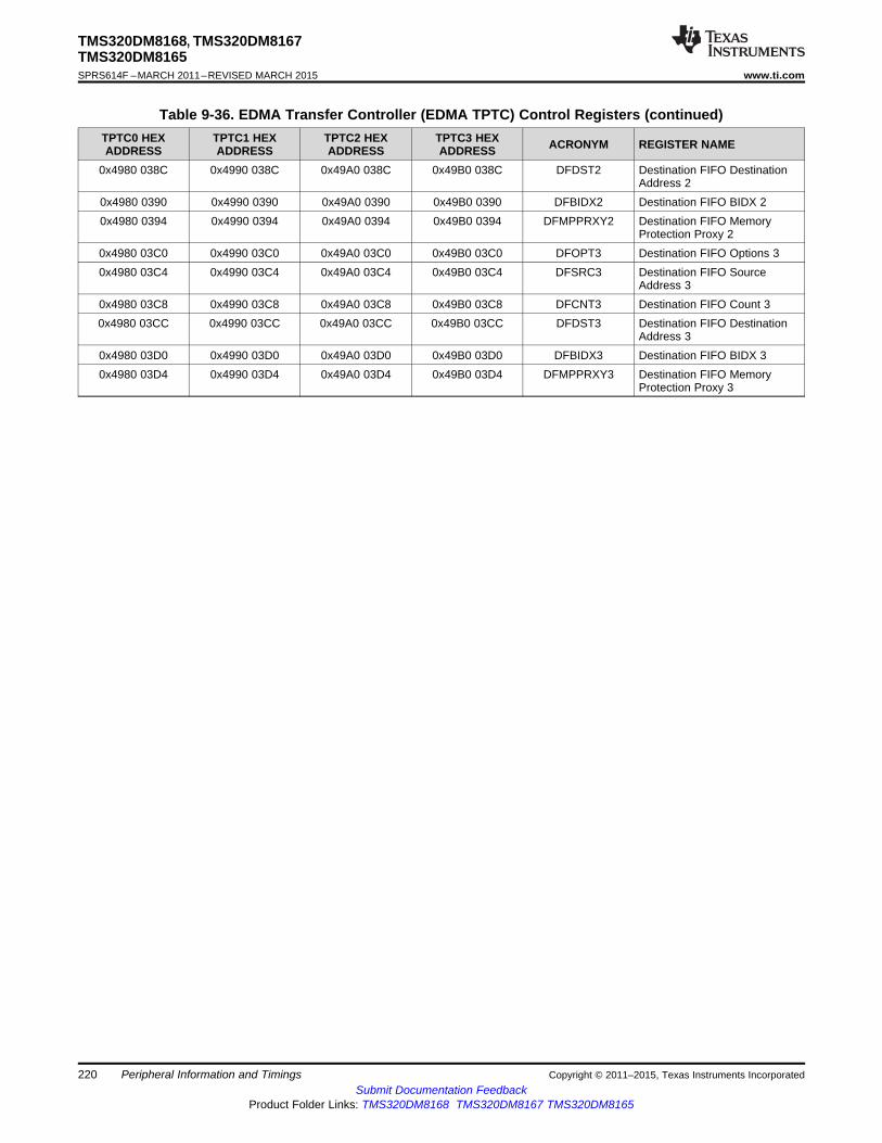
TMS320DM8168, TMS320DM8167TMS320DM8165SPRS614F –MARCH 2011–REVISED MARCH 2015 www.ti.com
Table 9-36. EDMA Transfer Controller (EDMA TPTC) Control Registers (continued)TPTC0 HEX TPTC1 HEX TPTC2 HEX TPTC3 HEX ACRONYM REGISTER NAMEADDRESS ADDRESS ADDRESS ADDRESS0x4980 038C 0x4990 038C 0x49A0 038C 0x49B0 038C DFDST2 Destination FIFO Destination
Address 20x4980 0390 0x4990 0390 0x49A0 0390 0x49B0 0390 DFBIDX2 Destination FIFO BIDX 20x4980 0394 0x4990 0394 0x49A0 0394 0x49B0 0394 DFMPPRXY2 Destination FIFO Memory
Protection Proxy 20x4980 03C0 0x4990 03C0 0x49A0 03C0 0x49B0 03C0 DFOPT3 Destination FIFO Options 30x4980 03C4 0x4990 03C4 0x49A0 03C4 0x49B0 03C4 DFSRC3 Destination FIFO Source
Address 30x4980 03C8 0x4990 03C8 0x49A0 03C8 0x49B0 03C8 DFCNT3 Destination FIFO Count 30x4980 03CC 0x4990 03CC 0x49A0 03CC 0x49B0 03CC DFDST3 Destination FIFO Destination
Address 30x4980 03D0 0x4990 03D0 0x49A0 03D0 0x49B0 03D0 DFBIDX3 Destination FIFO BIDX 30x4980 03D4 0x4990 03D4 0x49A0 03D4 0x49B0 03D4 DFMPPRXY3 Destination FIFO Memory
Protection Proxy 3
220 Peripheral Information and Timings Copyright © 2011–2015, Texas Instruments IncorporatedSubmit Documentation Feedback
Product Folder Links: TMS320DM8168 TMS320DM8167 TMS320DM8165

TMS320DM8168, TMS320DM8167TMS320DM8165
www.ti.com SPRS614F –MARCH 2011–REVISED MARCH 2015
9.6 Ethernet Media Access Controller (EMAC)The device includes two Ethernet Media Access Controller (EMAC) modules which provide an efficientinterface between the device and the networked community. The EMAC supports 10Base-T (10 Mbits persecond [Mbps]) and 100Base-TX (100 Mbps) in either half- or full-duplex mode, and 1000Base-T (1000Mbps) in full-duplex mode, with hardware flow control and quality-of-service (QOS) support. The EMACcontrols the flow of packet data from the device to an external PHY. A single MDIO interface is pinned outto control the PHY configuration and status monitoring. Multiple external PHYs can be controlled by theMDIO interface.
The EMAC module conforms to the IEEE 802.3-2002 standard, describing the Carrier Sense MultipleAccess with Collision Detection (CSMA/CD) Access Method and Physical Layer specifications. The IEEE802.3 standard has also been adopted by ISO/IEC and re-designated as ISO/IEC 8802-3:2000(E).Deviating from this standard, the EMAC module does not use the transmit coding error signal, MTXER.Instead of driving the error pin when an underflow condition occurs on a transmitted frame, the EMACintentionally generates an incorrect checksum by inverting the frame CRC so that the transmitted frame isdetected as an error by the network. In addition, the EMAC IOs operate at 3.3 V and are not compatiblewith 2.5-V IO signaling; therefore, only Ethernet PHYs with 3.3-V IO interface should be used. The EMACmodule incorporates 8K bytes of internal RAM to hold EMAC buffer descriptors and contains thenecessary components to enable the EMAC to make efficient use of device memory and control deviceinterrupts.
The EMAC module on the device supports two interface modes: Media Independent Interface (MII) andGigabit Media Independent Interface (GMII). The MII and GMII interface modes are defined in the IEEE802.3-2002 standard. The EMAC uses the same pins for the MII and GMII modes of operation. Only onemode can be used at a time.
The MII and GMII modes-of-operation pins are as follows:• MII: EMAC[1:0]_TXCLK, EMAC[1:0]_RXCLK, EMAC[1:0]_TXD[3:0], EMAC[1:0]_RXD[3:0],
EMAC[1:0]_TXEN, EMAC[1:0]_RXDV, EMAC[1:0]_RXER, EMAC[1:0]_COL, EMAC[1:0]_CRS,MDIO_MCLK, and MDIO_MDIO.
• GMII: EMAC[1:0]_GMTCLK, EMAC[1:0]_TXCLK, EMAC[1:0]_RXCLK, EMAC[1:0]_TXD[7:0],EMAC[1:0]_RXD[7:0], EMAC[1:0]_TXEN, EMAC[1:0]_RXDV, EMAC[1:0]_RXER, EMAC[1:0]_COL,EMAC[1:0]_CRS, MDIO_MCLK, and MDIO_MDIO.
For more detailed information on the EMAC module, see the EMAC and MDIO chapter in theTMS320DM816x DaVinci Digital Media Processors Technical Reference Manual (literature numberSPRUGX8).
9.6.1 EMAC Peripheral Register Descriptions
Table 9-37. EMAC Control Registers
EMAC0 HEX ADDRESS EMAC1 HEX ADDRESS ACRONYM REGISTER NAME0x4A10 0000 0x4A12 0000 TXIDVER Transmit Identification and Version0x4A10 0004 0x4A12 0004 TXCONTROL Transmit Control0x4A10 0008 0x4A12 0008 TXTEARDOWN Transmit Teardown0x4A10 0010 0x4A12 0010 RXIDVER Receive Identification and Version0x4A10 0014 0x4A12 0014 RXCONTROL Receive Control0x4A10 0018 0x4A12 0018 RXTEARDOWN Receive Teardown0x4A10 0080 0x4A12 0080 TXINTSTATRAW Transmit Interrupt Status (Unmasked)0x4A10 0084 0x4A12 0084 TXINTSTATMASKED Transmit Interrupt Status (Masked)0x4A10 0088 0x4A12 0088 TXINTMASKSET Transmit Interrupt Mask Set0x4A10 008C 0x4A12 008C TXINTMASKCLEAR Transmit Interrupt Clear0x4A10 0090 0x4A12 0090 MACINVECTOR MAC Input Vector0x4A10 0094 0x4A12 0094 MACEOIVECTOR MAC End of Interrupt Vector
Copyright © 2011–2015, Texas Instruments Incorporated Peripheral Information and Timings 221Submit Documentation Feedback
Product Folder Links: TMS320DM8168 TMS320DM8167 TMS320DM8165

TMS320DM8168, TMS320DM8167TMS320DM8165SPRS614F –MARCH 2011–REVISED MARCH 2015 www.ti.com
Table 9-37. EMAC Control Registers (continued)EMAC0 HEX ADDRESS EMAC1 HEX ADDRESS ACRONYM REGISTER NAME
0x4A10 00A0 0x4A12 00A0 RXINTSTATRAW Receive Interrupt Status (Unmasked)0x4A10 00A4 0x4A12 00A4 RXINTSTATMASKED Receive Interrupt Status (Masked)0x4A10 00A8 0x4A12 00A8 RXINTMASKSET Receive Interrupt Mask Set0x4A10 00AC 0x4A12 00AC RXINTMASKCLEAR Receive Interrupt Mask Clear0x4A10 00B0 0x4A12 00B0 MACINTSTATRAW MAC Interrupt Status (Unmasked)0x4A10 00B4 0x4A12 00B4 MACINTSTATMASKED MAC Interrupt Status (Masked)0x4A10 00B8 0x4A12 00B8 MACINTMASKSET MAC Interrupt Mask Set0x4A10 00BC 0x4A12 00BC MACINTMASKCLEAR MAC Interrupt Mask Clear0x4A10 0100 0x4A12 0100 RXMBPENABLE Receive Multicast, Broadcast,
Promiscuous Channel Enable0x4A10 0104 0x4A12 0104 RXUNICASTSET Receive Unicast Enable Set0x4A10 0108 0x4A12 0108 RXUNICASTCLEAR Receive Unicast Clear0x4A10 010C 0x4A12 010C RXMAXLEN Receive Maximum Length0x4A10 0110 0x4A12 0110 RXBUFFEROFFSET Receive Buffer Offset0x4A10 0114 0x4A12 0114 RXFILTERLOWTHRESH Receive Filter Low Priority Frame
Threshold0x4A10 0120 0x4A12 0120 RX0FLOWTHRESH Receive Channel 0 Flow Control
Threshold0x4A10 0124 0x4A12 0124 RX1FLOWTHRESH Receive Channel 1 Flow Control
Threshold0x4A10 0128 0x4A12 0128 RX2FLOWTHRESH Receive Channel 2 Flow Control
Threshold0x4A10 012C 0x4A12 012C RX3FLOWTHRESH Receive Channel 3 Flow Control
Threshold0x4A10 0130 0x4A12 0130 RX4FLOWTHRESH Receive Channel 4 Flow Control
Threshold0x4A10 0134 0x4A12 0134 RX5FLOWTHRESH Receive Channel 5 Flow Control
Threshold0x4A10 0138 0x4A12 0138 RX6FLOWTHRESH Receive Channel 6 Flow Control
Threshold0x4A10 013C 0x4A12 013C RX7FLOWTHRESH Receive Channel 7 Flow Control
Threshold0x4A10 0140 0x4A12 0140 RX0FREEBUFFER Receive Channel 0 Free Buffer Count0x4A10 0144 0x4A12 0144 RX1FREEBUFFER Receive Channel 1 Free Buffer Count0x4A10 0148 0x4A12 0148 RX2FREEBUFFER Receive Channel 2 Free Buffer Count0x4A10 014C 0x4A12 014C RX3FREEBUFFER Receive Channel 3 Free Buffer Count0x4A10 0150 0x4A12 0150 RX4FREEBUFFER Receive Channel 4 Free Buffer Count0x4A10 0154 0x4A12 0154 RX5FREEBUFFER Receive Channel 5 Free Buffer Count0x4A10 0158 0x4A12 0158 RX6FREEBUFFER Receive Channel 6 Free Buffer Count0x4A10 015C 0x4A12 015C RX7FREEBUFFER Receive Channel 7 Free Buffer Count0x4A10 0160 0x4A12 0160 MACCONTROL MAC Control0x4A10 0164 0x4A12 0164 MACSTATUS MAC Status0x4A10 0168 0x4A12 0168 EMCONTROL Emulation Control0x4A10 016C 0x4A12 016C FIFOCONTROL FIFO Control0x4A10 0170 0x4A12 0170 MACCONFIG MAC Configuration0x4A10 0174 0x4A12 0174 SOFTRESET Soft Reset0x4A10 01D0 0x4A12 01D0 MACSRCADDRLO MAC Source Address Low Bytes0x4A10 01D4 0x4A12 01D4 MACSRCADDRHI MAC Source Address High Bytes0x4A10 01D8 0x4A12 01D8 MACHASH1 MAC Hash Address 10x4A10 01DC 0x4A12 01DC MACHASH2 MAC Hash Address 2
222 Peripheral Information and Timings Copyright © 2011–2015, Texas Instruments IncorporatedSubmit Documentation Feedback
Product Folder Links: TMS320DM8168 TMS320DM8167 TMS320DM8165

TMS320DM8168, TMS320DM8167TMS320DM8165
www.ti.com SPRS614F –MARCH 2011–REVISED MARCH 2015
Table 9-37. EMAC Control Registers (continued)EMAC0 HEX ADDRESS EMAC1 HEX ADDRESS ACRONYM REGISTER NAME
0x4A10 01E0 0x4A12 01E0 BOFFTEST Back Off Test0x4A10 01E4 0x4A12 01E4 TPACETEST Transmit Pacing Algorithm Test0x4A10 01E8 0x4A12 01E8 RXPAUSE Receive Pause Timer0x4A10 01EC 0x4A12 01EC TXPAUSE Transmit Pause Timer
0x4A10 0200 - 0x4A10 02FC 0x4A12 0200 - 0x4A12 02FC (see Table 9-38) EMAC Network Statistics Registers0x4A10 0500 0x4A12 0500 MACADDRLO MAC Address Low Bytes, Used in
Receive Address Matching0x4A10 0504 0x4A12 0504 MACADDRHI MAC Address High Bytes, Used in
Receive Address Matching0x4A10 0508 0x4A12 0508 MACINDEX MAC Index0x4A10 0600 0x4A12 0600 TX0HDP Transmit Channel 0 DMA Head
Descriptor Pointer0x4A10 0604 0x4A12 0604 TX1HDP Transmit Channel 1 DMA Head
Descriptor Pointer0x4A10 0608 0x4A12 0608 TX2HDP Transmit Channel 2 DMA Head
Descriptor Pointer0x4A10 060C 0x4A12 060C TX3HDP Transmit Channel 3 DMA Head
Descriptor Pointer0x4A10 0610 0x4A12 0610 TX4HDP Transmit Channel 4 DMA Head
Descriptor Pointer0x4A10 0614 0x4A12 0614 TX5HDP Transmit Channel 5 DMA Head
Descriptor Pointer0x4A10 0618 0x4A12 0618 TX6HDP Transmit Channel 6 DMA Head
Descriptor Pointer0x4A10 061C 0x4A12 061C TX7HDP Transmit Channel 7 DMA Head
Descriptor Pointer0x4A10 0620 0x4A12 0620 RX0HDP Receive Channel 0 DMA Head
Descriptor Pointer0x4A10 0624 0x4A12 0624 RX1HDP Receive Channel 1 DMA Head
Descriptor Pointer0x4A10 0628 0x4A12 0628 RX2HDP Receive Channel 2 DMA Head
Descriptor Pointer0x4A10 062C 0x4A12 062C RX3HDP Receive Channel 3 DMA Head
Descriptor Pointer0x4A10 0630 0x4A12 0630 RX4HDP Receive Channel 4 DMA Head
Descriptor Pointer0x4A10 0634 0x4A12 0634 RX5HDP Receive Channel 5 DMA Head
Descriptor Pointer0x4A10 0638 0x4A12 0638 RX6HDP Receive Channel 6 DMA Head
Descriptor Pointer0x4A10 063C 0x4A12 063C RX7HDP Receive Channel 7 DMA Head
Descriptor Pointer0x4A10 0640 0x4A12 0640 TX0CP Transmit Channel 0 Completion
Pointer0x4A10 0644 0x4A12 0644 TX1CP Transmit Channel 1 Completion
Pointer0x4A10 0648 0x4A12 0648 TX2CP Transmit Channel 2 Completion
Pointer0x4A10 064C 0x4A12 064C TX3CP Transmit Channel 3 Completion
Pointer0x4A10 0650 0x4A12 0650 TX4CP Transmit Channel 4 Completion
Pointer0x4A10 0654 0x4A12 0654 TX5CP Transmit Channel 5 Completion
Pointer
Copyright © 2011–2015, Texas Instruments Incorporated Peripheral Information and Timings 223Submit Documentation Feedback
Product Folder Links: TMS320DM8168 TMS320DM8167 TMS320DM8165
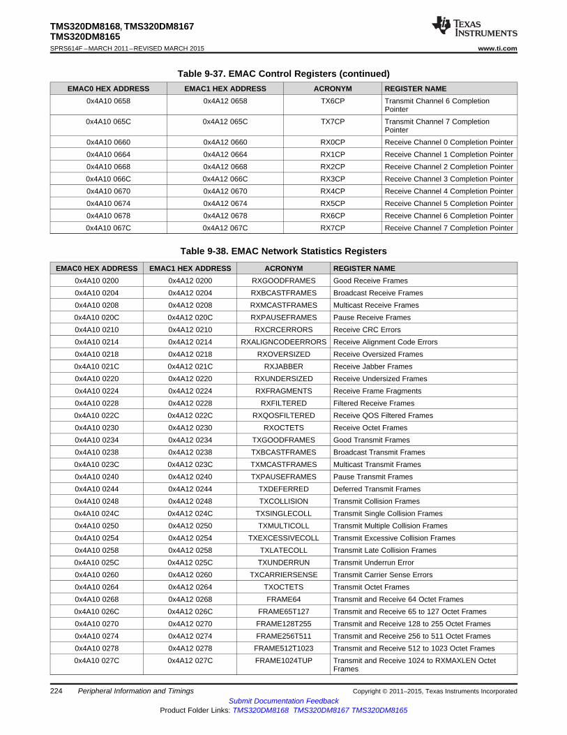
TMS320DM8168, TMS320DM8167TMS320DM8165SPRS614F –MARCH 2011–REVISED MARCH 2015 www.ti.com
Table 9-37. EMAC Control Registers (continued)EMAC0 HEX ADDRESS EMAC1 HEX ADDRESS ACRONYM REGISTER NAME
0x4A10 0658 0x4A12 0658 TX6CP Transmit Channel 6 CompletionPointer
0x4A10 065C 0x4A12 065C TX7CP Transmit Channel 7 CompletionPointer
0x4A10 0660 0x4A12 0660 RX0CP Receive Channel 0 Completion Pointer0x4A10 0664 0x4A12 0664 RX1CP Receive Channel 1 Completion Pointer0x4A10 0668 0x4A12 0668 RX2CP Receive Channel 2 Completion Pointer0x4A10 066C 0x4A12 066C RX3CP Receive Channel 3 Completion Pointer0x4A10 0670 0x4A12 0670 RX4CP Receive Channel 4 Completion Pointer0x4A10 0674 0x4A12 0674 RX5CP Receive Channel 5 Completion Pointer0x4A10 0678 0x4A12 0678 RX6CP Receive Channel 6 Completion Pointer0x4A10 067C 0x4A12 067C RX7CP Receive Channel 7 Completion Pointer
Table 9-38. EMAC Network Statistics Registers
EMAC0 HEX ADDRESS EMAC1 HEX ADDRESS ACRONYM REGISTER NAME0x4A10 0200 0x4A12 0200 RXGOODFRAMES Good Receive Frames0x4A10 0204 0x4A12 0204 RXBCASTFRAMES Broadcast Receive Frames0x4A10 0208 0x4A12 0208 RXMCASTFRAMES Multicast Receive Frames0x4A10 020C 0x4A12 020C RXPAUSEFRAMES Pause Receive Frames0x4A10 0210 0x4A12 0210 RXCRCERRORS Receive CRC Errors0x4A10 0214 0x4A12 0214 RXALIGNCODEERRORS Receive Alignment Code Errors0x4A10 0218 0x4A12 0218 RXOVERSIZED Receive Oversized Frames0x4A10 021C 0x4A12 021C RXJABBER Receive Jabber Frames0x4A10 0220 0x4A12 0220 RXUNDERSIZED Receive Undersized Frames0x4A10 0224 0x4A12 0224 RXFRAGMENTS Receive Frame Fragments0x4A10 0228 0x4A12 0228 RXFILTERED Filtered Receive Frames0x4A10 022C 0x4A12 022C RXQOSFILTERED Receive QOS Filtered Frames0x4A10 0230 0x4A12 0230 RXOCTETS Receive Octet Frames0x4A10 0234 0x4A12 0234 TXGOODFRAMES Good Transmit Frames0x4A10 0238 0x4A12 0238 TXBCASTFRAMES Broadcast Transmit Frames0x4A10 023C 0x4A12 023C TXMCASTFRAMES Multicast Transmit Frames0x4A10 0240 0x4A12 0240 TXPAUSEFRAMES Pause Transmit Frames0x4A10 0244 0x4A12 0244 TXDEFERRED Deferred Transmit Frames0x4A10 0248 0x4A12 0248 TXCOLLISION Transmit Collision Frames0x4A10 024C 0x4A12 024C TXSINGLECOLL Transmit Single Collision Frames0x4A10 0250 0x4A12 0250 TXMULTICOLL Transmit Multiple Collision Frames0x4A10 0254 0x4A12 0254 TXEXCESSIVECOLL Transmit Excessive Collision Frames0x4A10 0258 0x4A12 0258 TXLATECOLL Transmit Late Collision Frames0x4A10 025C 0x4A12 025C TXUNDERRUN Transmit Underrun Error0x4A10 0260 0x4A12 0260 TXCARRIERSENSE Transmit Carrier Sense Errors0x4A10 0264 0x4A12 0264 TXOCTETS Transmit Octet Frames0x4A10 0268 0x4A12 0268 FRAME64 Transmit and Receive 64 Octet Frames0x4A10 026C 0x4A12 026C FRAME65T127 Transmit and Receive 65 to 127 Octet Frames0x4A10 0270 0x4A12 0270 FRAME128T255 Transmit and Receive 128 to 255 Octet Frames0x4A10 0274 0x4A12 0274 FRAME256T511 Transmit and Receive 256 to 511 Octet Frames0x4A10 0278 0x4A12 0278 FRAME512T1023 Transmit and Receive 512 to 1023 Octet Frames0x4A10 027C 0x4A12 027C FRAME1024TUP Transmit and Receive 1024 to RXMAXLEN Octet
Frames
224 Peripheral Information and Timings Copyright © 2011–2015, Texas Instruments IncorporatedSubmit Documentation Feedback
Product Folder Links: TMS320DM8168 TMS320DM8167 TMS320DM8165
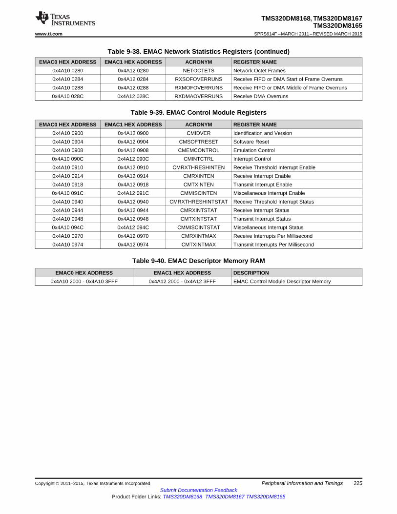
TMS320DM8168, TMS320DM8167TMS320DM8165
www.ti.com SPRS614F –MARCH 2011–REVISED MARCH 2015
Table 9-38. EMAC Network Statistics Registers (continued)EMAC0 HEX ADDRESS EMAC1 HEX ADDRESS ACRONYM REGISTER NAME
0x4A10 0280 0x4A12 0280 NETOCTETS Network Octet Frames0x4A10 0284 0x4A12 0284 RXSOFOVERRUNS Receive FIFO or DMA Start of Frame Overruns0x4A10 0288 0x4A12 0288 RXMOFOVERRUNS Receive FIFO or DMA Middle of Frame Overruns0x4A10 028C 0x4A12 028C RXDMAOVERRUNS Receive DMA Overruns
Table 9-39. EMAC Control Module Registers
EMAC0 HEX ADDRESS EMAC1 HEX ADDRESS ACRONYM REGISTER NAME0x4A10 0900 0x4A12 0900 CMIDVER Identification and Version0x4A10 0904 0x4A12 0904 CMSOFTRESET Software Reset0x4A10 0908 0x4A12 0908 CMEMCONTROL Emulation Control0x4A10 090C 0x4A12 090C CMINTCTRL Interrupt Control0x4A10 0910 0x4A12 0910 CMRXTHRESHINTEN Receive Threshold Interrupt Enable0x4A10 0914 0x4A12 0914 CMRXINTEN Receive Interrupt Enable0x4A10 0918 0x4A12 0918 CMTXINTEN Transmit Interrupt Enable0x4A10 091C 0x4A12 091C CMMISCINTEN Miscellaneous Interrupt Enable0x4A10 0940 0x4A12 0940 CMRXTHRESHINTSTAT Receive Threshold Interrupt Status0x4A10 0944 0x4A12 0944 CMRXINTSTAT Receive Interrupt Status0x4A10 0948 0x4A12 0948 CMTXINTSTAT Transmit Interrupt Status0x4A10 094C 0x4A12 094C CMMISCINTSTAT Miscellaneous Interrupt Status0x4A10 0970 0x4A12 0970 CMRXINTMAX Receive Interrupts Per Millisecond0x4A10 0974 0x4A12 0974 CMTXINTMAX Transmit Interrupts Per Millisecond
Table 9-40. EMAC Descriptor Memory RAM
EMAC0 HEX ADDRESS EMAC1 HEX ADDRESS DESCRIPTION0x4A10 2000 - 0x4A10 3FFF 0x4A12 2000 - 0x4A12 3FFF EMAC Control Module Descriptor Memory
Copyright © 2011–2015, Texas Instruments Incorporated Peripheral Information and Timings 225Submit Documentation Feedback
Product Folder Links: TMS320DM8168 TMS320DM8167 TMS320DM8165

EMAC[1:0]_TXCLK
2 3
1 4
4
EMAC[1:0]_RXCLK
2 3
1 4
4
TMS320DM8168, TMS320DM8167TMS320DM8165SPRS614F –MARCH 2011–REVISED MARCH 2015 www.ti.com
9.6.2 EMAC Electrical Data and Timing
Table 9-41. Timing Requirements for EMAC[1:0]_RXCLK - [G]MII Operation(see Figure 9-43)
1000 Mbps (1 Gbps) 100 Mbps 10 Mbps(GMII Only)NO. UNITMIN MAX MIN MAX MIN MAX
Cycle time,1 tc(RXCLK) 8 40 400 nsEMAC[1:0]_RXCLKPulse duration,2 tw(RXCLKH) 2.8 14 140 nsEMAC1:0]_RXCLK highPulse duration,3 tw(RXCLKL) 2.8 14 140 nsEMAC[1:0]_RXCLK lowTransition time,4 tt(RXCLK) 1 3 3 nsEMAC[1:0]_RXCLK
Figure 9-43. EMAC[1:0]_RXCLK Timing
Table 9-42. Timing Requirements for EMAC[1:0]_TXCLK - [G]MII Operation(see Figure 9-44)
1000 Mbps (1 Gbps) 100 Mbps 10 Mbps(GMII Only)NO. UNITMIN MAX MIN MAX MIN MAX
Cycle time,1 tc(TXCLK) 8 40 400 nsEMAC[1:0]_TXCLKPulse duration,2 tw(TXCLKH) 2.8 14 140 nsEMAC[1:0]_TXCLK highPulse duration,3 tw(TXCLKL) 2.8 14 140 nsEMAC[1:0]_TXCLK lowTransition time,4 tt(TXCLK) 1 3 3 nsEMAC[1:0]_TXCLK
Figure 9-44. EMAC[1:0]_TXCLK Timing
226 Peripheral Information and Timings Copyright © 2011–2015, Texas Instruments IncorporatedSubmit Documentation Feedback
Product Folder Links: TMS320DM8168 TMS320DM8167 TMS320DM8165
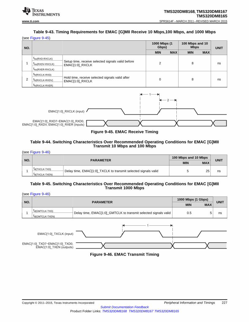
1
EMAC[1:0]_TXCLK (input)
EMAC[1:0]_ EMAC[1:0]_EMAC[1:0]_
TXD7− TXD0,TXEN (outputs)
EMAC[1:0]_RXCLK (input)
1
2
EMAC[1:0]_ EMAC[1:0]_EMAC[1:0]_ EMAC[1:0]_
RXD7− RXD0,RXDV, RXER (inputs)
TMS320DM8168, TMS320DM8167TMS320DM8165
www.ti.com SPRS614F –MARCH 2011–REVISED MARCH 2015
Table 9-43. Timing Requirements for EMAC [G]MII Receive 10 Mbps,100 Mbps, and 1000 Mbps(see Figure 9-45)
1000 Mbps (1 100 Mbps and 10Gbps) MbpsNO. UNIT
MIN MAX MIN MAXtsu(RXD-RXCLK)
Setup time, receive selected signals valid before1 tsu(RXDV-RXCLK) 2 8 nsEMAC[1:0]_RXCLKtsu(RXER-RXCLK)
th(RXCLK-RXD)Hold time, receive selected signals valid after2 th(RXCLK-RXDV) 0 8 nsEMAC[1:0]_RXCLK
th(RXCLK-RXER)
Figure 9-45. EMAC Receive Timing
Table 9-44. Switching Characteristics Over Recommended Operating Conditions for EMAC [G]MIITransmit 10 Mbps and 100 Mbps
(see Figure 9-46)100 Mbps and 10 Mbps
NO. PARAMETER UNITMIN MAX
td(TXCLK-TXD)1 Delay time, EMAC[1:0]_TXCLK to transmit selected signals valid 5 25 nstd(TXCLK-TXEN)
Table 9-45. Switching Characteristics Over Recommended Operating Conditions for EMAC [G]MIITransmit 1000 Mbps
(see Figure 9-46)1000 Mbps (1 Gbps)
NO. PARAMETER UNITMIN MAX
td(GMTCLK-TXD)1 Delay time, EMAC[1:0]_GMTCLK to transmit selected signals valid 0.5 5 nstd(GMTCLK-TXEN)
Figure 9-46. EMAC Transmit Timing
Copyright © 2011–2015, Texas Instruments Incorporated Peripheral Information and Timings 227Submit Documentation Feedback
Product Folder Links: TMS320DM8168 TMS320DM8167 TMS320DM8165

TMS320DM8168, TMS320DM8167TMS320DM8165SPRS614F –MARCH 2011–REVISED MARCH 2015 www.ti.com
9.6.3 Management Data Input and Output (MDIO)The Management Data Input and Output (MDIO) module continuously polls all 32 MDIO addresses inorder to enumerate all PHY devices in the system.
The MDIO module implements the 802.3 serial management interface to interrogate and control EthernetPHYs using a shared two-wire bus. Host software uses the MDIO module to configure the auto-negotiation parameters of each PHY attached to the EMAC, retrieve the negotiation results, and configurerequired parameters in the EMAC module for correct operation. The module is designed to allow almosttransparent operation of the MDIO interface, with very little maintenance from the core processor. A singleMDIO interface is pinned out to control the PHY configuration and status monitoring. Multiple externalPHYs can be controlled by the MDIO interface.
For more detailed information on the MDIO peripheral, see the EMAC and MDIO chapter in theTMS320DM816x DaVinci Digital Media Processors Technical Reference Manual (literature numberSPRUGX8).
9.6.3.1 MDIO Peripheral Register Descriptions
Table 9-46. MDIO Registers
HEX ADDRESS ACRONYM REGISTER NAME0x4A10 0800 VERSION MDIO Version0x4A10 0804 CONTROL MDIO Control0x4A10 0808 ALIVE PHY Alive Status0x4A10 080C LINK PHY Link Status0x4A10 0810 LINKINTRAW MDIO Link Status Change Interrupt (Unmasked)0x4A10 0814 LINKINTMASKED MDIO Link Status Change Interrupt (Masked)0x4A10 0818 - Reserved0x4A10 081C USERINTRAW MDIO User Command Complete Interrupt (Unmasked)0x4A10 0820 USERINTMASKED MDIO User Command Complete Interrupt (Masked)0x4A10 0824 USERINTMASKSET MDIO User Command Complete Interrupt Mask Set0x4A10 0828 USERINTMASKCLEAR MDIO User Command Complete Interrupt Mask Clear0x4A10 082C - Reserved0x4A10 0880 USERACCESS0 MDIO User Access 00x4A10 0884 USERPHYSEL0 MDIO User PHY Select 00x4A10 0888 USERACCESS1 MDIO User Access 10x4A10 088C USERPHYSEL1 MDIO User PHY Select 1
9.6.3.2 MDIO Electrical Data and Timing
Table 9-47. Timing Requirements for MDIO Input(see Figure 9-47)
NO. MIN MAX UNIT1 tc(MCLK) Cycle time, MDIO_MCLK 400 ns
tw(MCLK) Pulse duration, MDIO_MCLK high or low 180 ns4 tsu(MDIO-MCLKH) Setup time, MDIO_MDIO data input valid before MDIO_MCLK high 20 ns5 th(MCLKH-MDIO) Hold time, MDIO_MDIO data input valid after MDIO_MCLK high 0 ns
228 Peripheral Information and Timings Copyright © 2011–2015, Texas Instruments IncorporatedSubmit Documentation Feedback
Product Folder Links: TMS320DM8168 TMS320DM8167 TMS320DM8165

1
7
MDIO_MCLK
MDIO_MDIO(output)
1
4
5
MDIO_MCLK
MDIO_MDIO(input)
TMS320DM8168, TMS320DM8167TMS320DM8165
www.ti.com SPRS614F –MARCH 2011–REVISED MARCH 2015
Figure 9-47. MDIO Input Timing
Table 9-48. Switching Characteristics Over Recommended Operating Conditions for MDIO Output(see Figure 9-48)
NO. PARAMETER MIN MAX UNIT7 td(MCLKL-MDIO) Delay time, MDIO_MCLK low to MDIO_MDIO data output valid 100 ns
Figure 9-48. MDIO Output Timing
Copyright © 2011–2015, Texas Instruments Incorporated Peripheral Information and Timings 229Submit Documentation Feedback
Product Folder Links: TMS320DM8168 TMS320DM8167 TMS320DM8165

TMS320DM8168, TMS320DM8167TMS320DM8165SPRS614F –MARCH 2011–REVISED MARCH 2015 www.ti.com
9.7 General-Purpose Input and Output (GPIO)The GPIO peripheral provides general-purpose pins that can be configured as either inputs or outputs.When configured as an output, a write to an internal register controls the state driven on the output pin.When configured as an input, the state of the input is detectable by reading the state of an internalregister. In addition, the GPIO peripheral can produce CPU interrupts in different interrupt generationmodes. The GPIO peripheral provides generic connections to external devices.
The device contains two GPIO modules and each GPIO module is made up of 32 identical channels.
The device GPIO peripheral supports the following:• Up to 64 3.3-V GPIO pins, GP0[31:0] and GP1[31:0] (the exact number available varies as a function
of the device configuration). Each channel can be configured to be used in the following applications:– Data input and output– Keyboard interface with a de-bouncing cell– Synchronous interrupt generation (in active mode) upon the detection of external events (signal
transitions or signal levels).• Synchronous interrupt requests from each channel are processed by two identical interrupt generation
sub-modules to be used independently by the ARM or DSP. Interrupts can be triggered by rising orfalling edge, specified for each interrupt-capable GPIO signal.
• Shared registers can be accessed through "Set & Clear" protocol. Software writes 1 to correspondingbit positions to set or to clear GPIO signals. This allows multiple software processes to toggle GPIOoutput signals without critical section protection (disable interrupts, program GPIO, re-enable interrupts,to prevent context switching to another process during GPIO programming).
• Separate input and output registers.• Output register in addition to set or clear so that, if preferred by software, some GPIO output signals
can be toggled by direct write to the output registers.• Output register, when read, reflects output drive status. This, in addition to the input register reflecting
pin status and open-drain IO cell, allows wired logic to be implemented.
For more detailed information on GPIOs, see the GPIO chapter in the TMS320DM816x DaVinci DigitalMedia Processors Technical Reference Manual (literature number SPRUGX8).
9.7.1 GPIO Peripheral Register Descriptions
Table 9-49. GPIO Registers
GPIO0 HEX ADDRESS GPIO1 HEX ADDRESS ACRONYM REGISTER NAME0x4803 2000 0x4804 C000 GPIO_REVISION GPIO Revision0x4803 2010 0x4804 C010 GPIO_SYSCONFIG System Configuration0x4803 2020 0x4804 C020 GPIO_EOI End of Interrupt0x4803 2024 0x4804 C024 GPIO_IRQSTATUS_RAW_0 Status Raw for Interrupt 10x4803 2028 0x4804 C028 GPIO_IRQSTATUS_RAW_1 Status Raw for Interrupt 20x4803 202C 0x4804 C02C GPIO_IRQSTATUS_0 Status for Interrupt 10x4803 2030 0x4804 C030 GPIO_IRQSTATUS_1 Status for Interrupt 20x4803 2034 0x4804 C034 GPIO_IRQSTATUS_SET_0 Enable Set for Interrupt 10x4803 2038 0x4804 C038 GPIO_IRQSTATUS_SET_1 Enable Set for Interrupt 20x4803 203C 0x4804 C03C GPIO_IRQSTATUS_CLR_0 Enable Clear for Interrupt 10x4803 2040 0x4804 C040 GPIO_IRQSTATUS_CLR_1 Enable Clear for Interrupt 20x4803 2044 0x4804 C044 GPIO_IRQWAKEN_0 Wakeup Enable for Interrupt 10x4803 2048 0x4804 C048 GPIO_IRQWAKEN_1 Wakeup Enable for Interrupt 20x4803 2114 0x4804 C114 GPIO_SYSSTATUS System Status0x4803 2130 0x4804 C130 GPIO_CTRL Module Control0x4803 2134 0x4804 C134 GPIO_OE Output Enable
230 Peripheral Information and Timings Copyright © 2011–2015, Texas Instruments IncorporatedSubmit Documentation Feedback
Product Folder Links: TMS320DM8168 TMS320DM8167 TMS320DM8165
TMS320DM8168, TMS320DM8167TMS320DM8165
www.ti.com SPRS614F –MARCH 2011–REVISED MARCH 2015
Table 9-49. GPIO Registers (continued)GPIO0 HEX ADDRESS GPIO1 HEX ADDRESS ACRONYM REGISTER NAME
0x4803 2138 0x4804 C138 GPIO_DATAIN Data Input0x4803 213C 0x4804 C13C GPIO_DATAOUT Data Output0x4803 2140 0x4804 C140 GPIO_LEVELDETECT0 Detect Low Level0x4803 2144 0x4804 C144 GPIO_LEVELDETECT1 Detect High Level0x4803 2148 0x4804 C148 GPIO_RISINGDETECT Detect Rising Edge0x4803 214C 0x4804 C14C GPIO_FALLINGDETECT Detect Falling Edge0x4803 2150 0x4804 C150 GPIO_DEBOUNCENABLE Debouncing Enable0x4803 2154 0x4804 C154 GPIO_DEBOUNCINGTIME Debouncing Value0x4803 2190 0x4804 C190 GPIO_CLEARDATAOUT Clear Data Output0x4803 2194 0x4804 C194 GPIO_SETDATAOUT Set Data Output
Copyright © 2011–2015, Texas Instruments Incorporated Peripheral Information and Timings 231Submit Documentation Feedback
Product Folder Links: TMS320DM8168 TMS320DM8167 TMS320DM8165

GP[1:0][x]input
4
3
2
1
GP[1:0][x]output
TMS320DM8168, TMS320DM8167TMS320DM8165SPRS614F –MARCH 2011–REVISED MARCH 2015 www.ti.com
9.7.2 GPIO Electrical Data and Timing
Table 9-50. Timing Requirements for GPIO Inputs(see Figure 9-49)
NO. MIN MAX UNIT1 tw(GPIH) Pulse duration, GP[x] input high 12P (1) ns2 tw(GPIL) Pulse duration, GP[x] input low 12P (1) ns
(1) P = Module clock.
Table 9-51. Switching Characteristics Over Recommended Operating Conditions for GPIO Outputs(see Figure 9-49)
NO. PARAMETER MIN MAX UNIT3 tw(GPOH) Pulse duration, GP[x] output high 36P-8 (1) ns4 tw(GPOL) Pulse duration, GP[x] output low 36P-8 (1) ns
(1) P = Module clock.
Figure 9-49. GPIO Port Timing
232 Peripheral Information and Timings Copyright © 2011–2015, Texas Instruments IncorporatedSubmit Documentation Feedback
Product Folder Links: TMS320DM8168 TMS320DM8167 TMS320DM8165

TMS320DM8168, TMS320DM8167TMS320DM8165
www.ti.com SPRS614F –MARCH 2011–REVISED MARCH 2015
9.8 General-Purpose Memory Controller (GPMC) and Error Locator Module (ELM)The GPMC is a device memory controller used to provide a glueless interface to external memory devicessuch as NOR Flash, NAND Flash (with BCH and Hamming Error Code Detection for 8-bit or 16-bit NANDFlash), SRAM, and Pseudo-SRAM. It includes flexible asynchronous protocol control for interface toSRAM-like memories and custom logic (FPGA, CPLD, ASICs, and others).
The first section of GPMC memory (0x0 - 0x00FF_FFFF) is reserved for BOOTROM. Accessible memorystarts at location 0x0100_0000.
Other supported features include:• 8-bit and 6-bit wide multiplexed address and data bus• Up to 6 chip selects with up to 256M-byte address space per chip select pin• Non-multiplexed address and data mode• Pre-fetch and write posting engine associated with system DMA to get full performance from NAND
device with minimum impact on NOR and SRAM concurrent access.
The device also contains an Error Locator Module (ELM) which is used to extract error addresses fromsyndrome polynomials generated using a BCH algorithm. Each of these polynomials gives a status of theread operations for a 512 bytes block from a NAND flash and its associated BCH parity bits, plusoptionally spare area information. The ELM has the following features:• 4-bit, 8-bit, and 16-bit per 512-byte block error location based on BCH algorithms• Eight simultaneous processing contexts• Page-based and continuous modes• Interrupt generation on error location process completion
– When the full page has been processed in page mode– For each syndrome polynomial in continuous mode.
For more detailed information on the GPMC, see the GPMC chapter in the TMS320DM816x DaVinciDigital Media Processors Technical Reference Manual (literature number SPRUGX8).
9.8.1 GPMC and ELM Peripheral Register Descriptions
Table 9-52. GPMC Registers (1) (2)
HEX ADDRESS ACRONYM REGISTER NAME0x5000 0000 GPMC_REVISION GPIO Revision0x5000 0010 GPMC_SYSCONFIG System Configuration0x5000 0014 GPMC_SYSSTATUS System Status0x5000 0018 GPMC_IRQSTATUS Status for Interrupt0x5000 001C GPMC_IRQENABLE Interrupt Enable0x5000 0040 GPMC_TIMEOUT_CONTROL Timeout Counter Start Value0x5000 0044 GPMC_ERR_ADDRESS Error Address0x5000 0048 GPMC_ERR_TYPE Error Type0x5000 0050 GPMC_CONFIG GPMC Global Configuration0x5000 0054 GPMC_STATUS GPMC Global Status
0x5000 0060 + (0x0000 0030 * i) GPMC_CONFIG1_0 - Parameter Configuration 1_0-5GPMC_CONFIG1_5
0x5000 0064 + (0x0000 0030 * i) GPMC_CONFIG2_0 - Parameter Configuration 2_0-5GPMC_CONFIG2_5
0x5000 0068 + (0x0000 0030 * i) GPMC_CONFIG3_0 - Parameter Configuration 3_0-5GPMC_CONFIG3_5
0x5000 006C + (0x0000 0030 * i) GPMC_CONFIG4_0 - Parameter Configuration 4_0-5GPMC_CONFIG4_5
(1) i = 0 to 5.(2) j = 0 to 8.
Copyright © 2011–2015, Texas Instruments Incorporated Peripheral Information and Timings 233Submit Documentation Feedback
Product Folder Links: TMS320DM8168 TMS320DM8167 TMS320DM8165

TMS320DM8168, TMS320DM8167TMS320DM8165SPRS614F –MARCH 2011–REVISED MARCH 2015 www.ti.com
Table 9-52. GPMC Registers(1)(2) (continued)HEX ADDRESS ACRONYM REGISTER NAME
0x5000 0070 + (0x0000 0030 * i) GPMC_CONFIG5_0 - Parameter Configuration 5_0-5GPMC_CONFIG5_5
0x5000 0074 + (0x0000 0030 * i) GPMC_CONFIG6_0 - Parameter Configuration 6_0-5GPMC_CONFIG6_5
0x5000 0078 + (0x0000 0030 * i) GPMC_CONFIG7_0 - Parameter Configuration 7_0-5GPMC_CONFIG7_5
0x5000 007C + (0x0000 0030 * i) GPMC_NAND_COMMAND_0 - NAND Command 0-5GPMC_NAND_COMMAND_5
0x5000 0080 + (0x0000 0030 * i) GPMC_NAND_ADDRESS_0 - NAND Address 0-5GPMC_NAND_ADDRESS_5
0x5000 0084 + (0x0000 0030 * i) GPMC_NAND_DATA_0 - NAND Data 0-5GPMC_NAND_DATA_5
0x5000 01E0 GPMC_PREFETCH_CONFIG1 Prefetch Configuration 10x5000 01E4 GPMC_PREFETCH_CONFIG2 Prefetch Configuration 20x5000 01EC GPMC_PREFETCH_CONTROL Prefetch Control0x5000 01F0 GPMC_PREFETCH_STATUS Prefetch Status0x5000 01F4 GPMC_ECC_CONFIG ECC Configuration0x5000 01F8 GPMC_ECC_CONTROL ECC Control0x5000 01FC GPMC_ECC_SIZE_CONFIG ECC Size Configuration
0x5000 0200 + (0x0000 0004 * j) GPMC_ECC0_RESULT - ECC0-8 ResultGPMC_ECC8_RESULT
0x5000 0240 + (0x0000 0010 * i) GPMC_BCH_RESULT0_0 - BCH Result 0_0-5GPMC_BCH_RESULT0_5
0x5000 0244 + (0x0000 0010 * i) GPMC_BCH_RESULT1_0 - BCH Result 1_0-5GPMC_BCH_RESULT1_5
0x5000 0248 + (0x0000 0010 * i) GPMC_BCH_RESULT2_0 - BCH Result 2_0-5GPMC_BCH_RESULT2_5
0x5000 024C + (0x0000 0010 * i) GPMC_BCH_RESULT3_0 - BCH Result 3_0-5GPMC_BCH_RESULT3_5
0x5000 0300 + (0x0000 0010 * i) GPMC_BCH_RESULT4_0 - BCH Result 4_0-5GPMC_BCH_RESULT4_5
0x5000 0304 + (0x0000 0010 * i) GPMC_BCH_RESULT5_0 - BCH Result 5_0-5GPMC_BCH_RESULT5_5
0x5000 0308 + (0x0000 0010 * i) GPMC_BCH_RESULT6_0 - BCH Result 6_0-5GPMC_BCH_RESULT6_5
0x5000 02D0 GPMC_BCH_SWDATA BCH Data
Table 9-53. ELM Registers (1)
HEX ADDRESS ACRONYM REGISTER NAME0x4808 0000 ELM_REVISION Revision0x4808 0010 ELM_SYSCONFIG Configuration0x4808 0014 ELM_SYSSTATUS Status0x4808 0018 ELM_IRQSTATUS Interrupt status0x4808 001C ELM_IRQENABLE Interrupt enable0x4808 0020 ELM_LOCATION_CONFIG ECC algorithm parameters0x4808 0080 ELM_PAGE_CTRL Page definition
0x4808 0400 + (0x40 * i) ELM_SYNDROME_FRAGMENT_0_i Input syndrome polynomial bits 0 to 310x4808 0404 + (0x40 * i) ELM_SYNDROME_FRAGMENT_1_i Input syndrome polynomial bits 32 to 630x4808 0408 + (0x40 * i) ELM_SYNDROME_FRAGMENT_2_i Input syndrome polynomial bits 64 to 950x4808 040C + (0x40 * i) ELM_SYNDROME_FRAGMENT_3_i Input syndrome polynomial bits 96 to 1270x4808 0410 + (0x40 * i) ELM_SYNDROME_FRAGMENT_4_i Input syndrome polynomial bits 128 to 159
(1) i = 0 to 7.
234 Peripheral Information and Timings Copyright © 2011–2015, Texas Instruments IncorporatedSubmit Documentation Feedback
Product Folder Links: TMS320DM8168 TMS320DM8167 TMS320DM8165

TMS320DM8168, TMS320DM8167TMS320DM8165
www.ti.com SPRS614F –MARCH 2011–REVISED MARCH 2015
Table 9-53. ELM Registers(1) (continued)HEX ADDRESS ACRONYM REGISTER NAME
0x4808 0414 + (0x40 * i) ELM_SYNDROME_FRAGMENT_5_i Input syndrome polynomial bits 160 to 1910x4808 0418 + (0x40 * i) ELM_SYNDROME_FRAGMENT_6_i Input syndrome polynomial bits 192 to 2070x4808 0800 + (0x100 * i) ELM_LOCATION_STATUS_i Exit status0x4808 0880 + (0x100 * i) ELM_ERROR_LOCATION_0_i Error location0x4808 0884 + (0x100 * i) ELM_ERROR_LOCATION_1_i Error location0x4808 0888 + (0x100 * i) ELM_ERROR_LOCATION_2_i Error location0x4808 088C + (0x100 * i) ELM_ERROR_LOCATION_3_i Error location0x4808 0890 + (0x100 * i) ELM_ERROR_LOCATION_4_i Error location0x4808 0894 + (0x100 * i) ELM_ERROR_LOCATION_5_i Error location0x4808 0898 + (0x100 * i) ELM_ERROR_LOCATION_6_i Error location0x4808 089C + (0x100 * i) ELM_ERROR_LOCATION_7_i Error location0x4808 08A0 + (0x100 * i) ELM_ERROR_LOCATION_8_i Error location0x4808 08A4 + (0x100 * i) ELM_ERROR_LOCATION_9_i Error location0x4808 08A8 + (0x100 * i) ELM_ERROR_LOCATION_10_i Error location0x4808 08AC + (0x100 * i) ELM_ERROR_LOCATION_11_i Error location0x4808 08B0 + (0x100 * i) ELM_ERROR_LOCATION_12_i Error location0x4808 08B4 + (0x100 * i) ELM_ERROR_LOCATION_13_i Error location0x4808 08B8 + (0x100 * i) ELM_ERROR_LOCATION_14_i Error location0x4808 08BC + (0x100 * i) ELM_ERROR_LOCATION_15_i Error location
Copyright © 2011–2015, Texas Instruments Incorporated Peripheral Information and Timings 235Submit Documentation Feedback
Product Folder Links: TMS320DM8168 TMS320DM8167 TMS320DM8165

TMS320DM8168, TMS320DM8167TMS320DM8165SPRS614F –MARCH 2011–REVISED MARCH 2015 www.ti.com
9.8.2 GPMC Electrical Data and Timing
9.8.2.1 GPMC and NOR Flash Interface Synchronous Mode Timing
Table 9-54. Timing Requirements for GPMC and NOR Flash Interface - Synchronous Mode(see Figure 9-50, Figure 9-51, Figure 9-52, Figure 9-53, Figure 9-54, Figure 9-55)
NO. MIN MAX UNIT13 tsu(DV-CLKH) Setup time, read GPMC_D[15:0] valid before GPMC_CLK high 3.2 ns14 th(CLKH-DV) Hold time, read GPMC_D[15:0] valid after GPMC_CLK high 2.5 ns22 tsu(WAITV-CLKH) Setup time, GPMC_WAIT valid before GPMC_CLK high 3.2 ns23 th(CLKH-WAITV) Hold time, GPMC_WAIT valid after GPMC_CLK high 2.5 ns
Table 9-55. Switching Characteristics Over Recommended Operating Conditions for GPMC and NORFlash Interface - Synchronous Mode
(see Figure 9-50, Figure 9-51, Figure 9-52, Figure 9-53, Figure 9-54, Figure 9-55)NO. PARAMETER MIN MAX UNIT
1 tc(CLK) Cycle time, output clock GPMC_CLK period 16 (1) nstw(CLKH) Pulse duration, output clock GPMC_CLK high 0.5P (2)
2 nstw(CLKL) Pulse duration, output clock GPMC_CLK low 0.5P (2)
3 td(CLKH-nCSV) Delay time, GPMC_CLK rising edge to GPMC_CS[x] transition F - 2.2 (3) F + 4.5 (3) ns4 td(CLKH-nCSIV) Delay time, GPMC_CLK rising edge to GPMC_CS[x] invalid E - 2.2 (4) E + 4.5 (4) ns
Delay time, GPMC_A[27:0] address bus valid to GPMC_CLK first5 td(ADDV-CLK) B - 4.5 (5) B + 2.3 (5) nsedgeDelay time, GPMC_CLK rising edge to GPMC_A[27:0] GPMC6 td(CLKH-ADDIV) -2.3 nsaddress bus invalidDelay time, GPMC_BE0_CLE, GPMC_BE1 valid to GPMC_CLK7 td(nBEV-CLK) B - 1.9 (5) B + 2.3 (5) nsfirst edgeDelay time, GPMC_CLK rising edge to GPMC_BE0_CLE,8 td(CLKH-nBEIV) D - 2.3 (6) D + 1.9 (6) nsGPMC_BE1 invalid
(1) Sync mode = 62.5 MHz; Async mode = 125 MHz.(2) P = GPMC_CLK period.(3) For nCS falling edge (CS activated):
• For GpmcFCLKDivider = 0:F = 0.5 * CSExtraDelay * GPMC_FCLK
• For GpmcFCLKDivider = 1:F = 0.5 * CSExtraDelay * GPMC_FCLK if (ClkActivationTime and CSOnTime are odd) or (ClkActivationTime and CSOnTime areeven)F = (1 + 0.5 * CSExtraDelay) * GPMC_FCLK otherwise
• For GpmcFCLKDivider = 2:F = 0.5 * CSExtraDelay * GPMC_FCLK if ((CSOnTime - ClkActivationTime) is a multiple of 3)F = (1 + 0.5 * CSExtraDelay) * GPMC_FCLK if ((CSOnTime - ClkActivationTime - 1) is a multiple of 3)F = (2 + 0.5 * CSExtraDelay) * GPMC_FCLK if ((CSOnTime - ClkActivationTime - 2) is a multiple of 3)
(4) For single read: E = (CSRdOffTime - AccessTime) * (TimeParaGranularity + 1) * GPMC_FCLKFor burst read: E = (CSRdOffTime - AccessTime) * (TimeParaGranularity + 1) * GPMC_FCLKFor burst write: E = (CSWrOffTime - AccessTime) * (TimeParaGranularity + 1) * GPMC_FCLK
(5) B = ClkActivationTime * GPMC_FCLK(6) For single read: D = (RdCycleTime - AccessTime) * (TimeParaGranularity + 1) * GPMC_FCLK
For burst read: D = (RdCycleTime - AccessTime) * (TimeParaGranularity + 1) * GPMC_FCLKFor burst write: D = (WrCycleTime - AccessTime) * (TimeParaGranularity + 1) * GPMC_FCLK
236 Peripheral Information and Timings Copyright © 2011–2015, Texas Instruments IncorporatedSubmit Documentation Feedback
Product Folder Links: TMS320DM8168 TMS320DM8167 TMS320DM8165
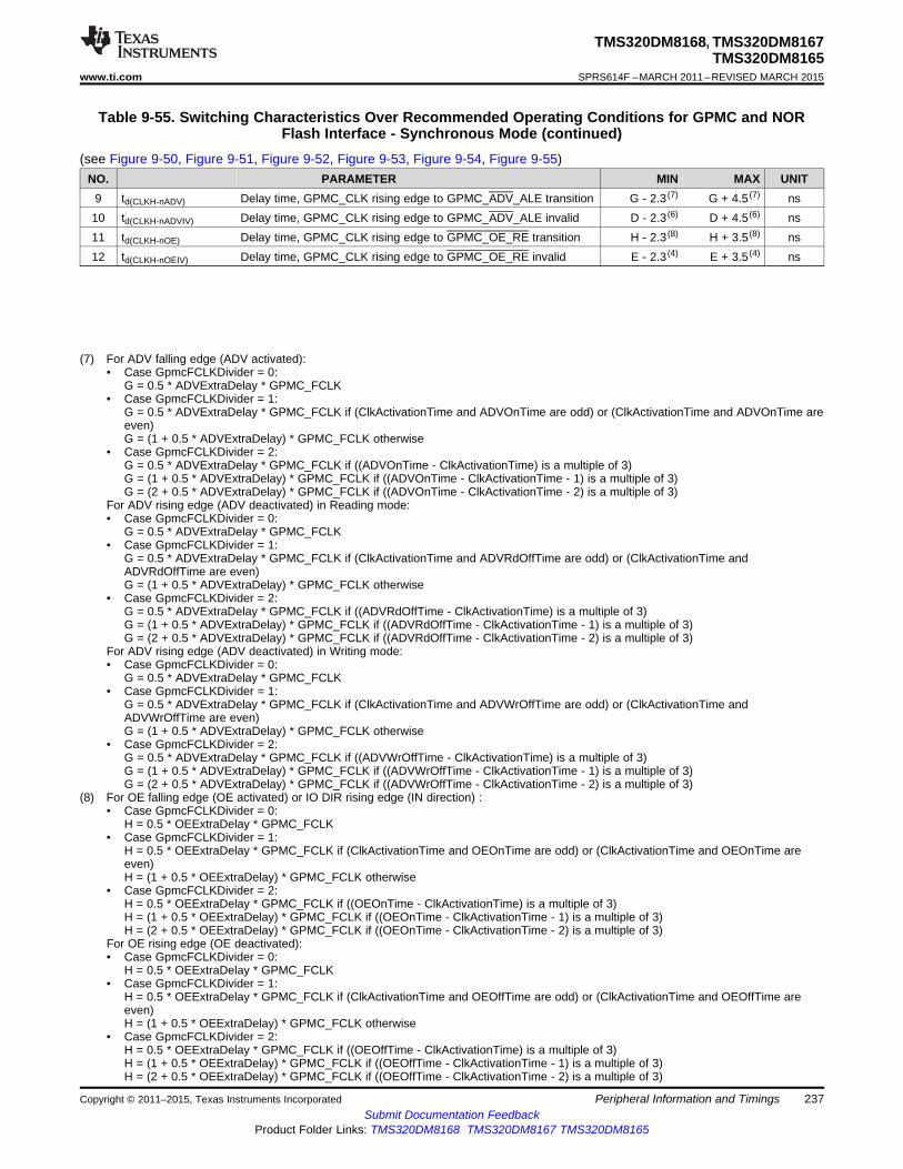
TMS320DM8168, TMS320DM8167TMS320DM8165
www.ti.com SPRS614F –MARCH 2011–REVISED MARCH 2015
Table 9-55. Switching Characteristics Over Recommended Operating Conditions for GPMC and NORFlash Interface - Synchronous Mode (continued)
(see Figure 9-50, Figure 9-51, Figure 9-52, Figure 9-53, Figure 9-54, Figure 9-55)NO. PARAMETER MIN MAX UNIT
9 td(CLKH-nADV) Delay time, GPMC_CLK rising edge to GPMC_ADV_ALE transition G - 2.3 (7) G + 4.5 (7) ns10 td(CLKH-nADVIV) Delay time, GPMC_CLK rising edge to GPMC_ADV_ALE invalid D - 2.3 (6) D + 4.5 (6) ns11 td(CLKH-nOE) Delay time, GPMC_CLK rising edge to GPMC_OE_RE transition H - 2.3 (8) H + 3.5 (8) ns12 td(CLKH-nOEIV) Delay time, GPMC_CLK rising edge to GPMC_OE_RE invalid E - 2.3 (4) E + 3.5 (4) ns
(7) For ADV falling edge (ADV activated):• Case GpmcFCLKDivider = 0:
G = 0.5 * ADVExtraDelay * GPMC_FCLK• Case GpmcFCLKDivider = 1:
G = 0.5 * ADVExtraDelay * GPMC_FCLK if (ClkActivationTime and ADVOnTime are odd) or (ClkActivationTime and ADVOnTime areeven)G = (1 + 0.5 * ADVExtraDelay) * GPMC_FCLK otherwise
• Case GpmcFCLKDivider = 2:G = 0.5 * ADVExtraDelay * GPMC_FCLK if ((ADVOnTime - ClkActivationTime) is a multiple of 3)G = (1 + 0.5 * ADVExtraDelay) * GPMC_FCLK if ((ADVOnTime - ClkActivationTime - 1) is a multiple of 3)G = (2 + 0.5 * ADVExtraDelay) * GPMC_FCLK if ((ADVOnTime - ClkActivationTime - 2) is a multiple of 3)
For ADV rising edge (ADV deactivated) in Reading mode:• Case GpmcFCLKDivider = 0:
G = 0.5 * ADVExtraDelay * GPMC_FCLK• Case GpmcFCLKDivider = 1:
G = 0.5 * ADVExtraDelay * GPMC_FCLK if (ClkActivationTime and ADVRdOffTime are odd) or (ClkActivationTime andADVRdOffTime are even)G = (1 + 0.5 * ADVExtraDelay) * GPMC_FCLK otherwise
• Case GpmcFCLKDivider = 2:G = 0.5 * ADVExtraDelay * GPMC_FCLK if ((ADVRdOffTime - ClkActivationTime) is a multiple of 3)G = (1 + 0.5 * ADVExtraDelay) * GPMC_FCLK if ((ADVRdOffTime - ClkActivationTime - 1) is a multiple of 3)G = (2 + 0.5 * ADVExtraDelay) * GPMC_FCLK if ((ADVRdOffTime - ClkActivationTime - 2) is a multiple of 3)
For ADV rising edge (ADV deactivated) in Writing mode:• Case GpmcFCLKDivider = 0:
G = 0.5 * ADVExtraDelay * GPMC_FCLK• Case GpmcFCLKDivider = 1:
G = 0.5 * ADVExtraDelay * GPMC_FCLK if (ClkActivationTime and ADVWrOffTime are odd) or (ClkActivationTime andADVWrOffTime are even)G = (1 + 0.5 * ADVExtraDelay) * GPMC_FCLK otherwise
• Case GpmcFCLKDivider = 2:G = 0.5 * ADVExtraDelay * GPMC_FCLK if ((ADVWrOffTime - ClkActivationTime) is a multiple of 3)G = (1 + 0.5 * ADVExtraDelay) * GPMC_FCLK if ((ADVWrOffTime - ClkActivationTime - 1) is a multiple of 3)G = (2 + 0.5 * ADVExtraDelay) * GPMC_FCLK if ((ADVWrOffTime - ClkActivationTime - 2) is a multiple of 3)
(8) For OE falling edge (OE activated) or IO DIR rising edge (IN direction) :• Case GpmcFCLKDivider = 0:
H = 0.5 * OEExtraDelay * GPMC_FCLK• Case GpmcFCLKDivider = 1:
H = 0.5 * OEExtraDelay * GPMC_FCLK if (ClkActivationTime and OEOnTime are odd) or (ClkActivationTime and OEOnTime areeven)H = (1 + 0.5 * OEExtraDelay) * GPMC_FCLK otherwise
• Case GpmcFCLKDivider = 2:H = 0.5 * OEExtraDelay * GPMC_FCLK if ((OEOnTime - ClkActivationTime) is a multiple of 3)H = (1 + 0.5 * OEExtraDelay) * GPMC_FCLK if ((OEOnTime - ClkActivationTime - 1) is a multiple of 3)H = (2 + 0.5 * OEExtraDelay) * GPMC_FCLK if ((OEOnTime - ClkActivationTime - 2) is a multiple of 3)
For OE rising edge (OE deactivated):• Case GpmcFCLKDivider = 0:
H = 0.5 * OEExtraDelay * GPMC_FCLK• Case GpmcFCLKDivider = 1:
H = 0.5 * OEExtraDelay * GPMC_FCLK if (ClkActivationTime and OEOffTime are odd) or (ClkActivationTime and OEOffTime areeven)H = (1 + 0.5 * OEExtraDelay) * GPMC_FCLK otherwise
• Case GpmcFCLKDivider = 2:H = 0.5 * OEExtraDelay * GPMC_FCLK if ((OEOffTime - ClkActivationTime) is a multiple of 3)H = (1 + 0.5 * OEExtraDelay) * GPMC_FCLK if ((OEOffTime - ClkActivationTime - 1) is a multiple of 3)H = (2 + 0.5 * OEExtraDelay) * GPMC_FCLK if ((OEOffTime - ClkActivationTime - 2) is a multiple of 3)
Copyright © 2011–2015, Texas Instruments Incorporated Peripheral Information and Timings 237Submit Documentation Feedback
Product Folder Links: TMS320DM8168 TMS320DM8167 TMS320DM8165

TMS320DM8168, TMS320DM8167TMS320DM8165SPRS614F –MARCH 2011–REVISED MARCH 2015 www.ti.com
Table 9-55. Switching Characteristics Over Recommended Operating Conditions for GPMC and NORFlash Interface - Synchronous Mode (continued)
(see Figure 9-50, Figure 9-51, Figure 9-52, Figure 9-53, Figure 9-54, Figure 9-55)NO. PARAMETER MIN MAX UNIT15 td(CLKH-nWE) Delay time, GPMC_CLK rising edge to GPMC_WE transition I - 2.3 (9) I + 4.5 (9) ns
Delay time, GPMC_CLK rising edge to GPMC_D[15:0] data bus16 td(CLKH-Data) J - 2.3 (10) J + 1.9 (10) nstransitionDelay time, GPMC_CLK rising edge to GPMC_BE0_CLE,18 td(CLKH-nBE) J - 2.3 (10) J + 1.9 (10) nsGPMC_BE1 transition
19 tw(nCSV) Pulse duration, GPMC_CS[x] low A (11) ns20 tw(nBEV) Pulse duration, GPMC_BE0_CLE, GPMC_BE1 low C (12) ns21 tw(nADVV) Pulse duration, GPMC_ADV_ALE low K (13) ns
Delay time, GPMC_CLK rising edge to GPMC_DIR high (IN24 td(CLKH-DIR) H - 2.3 (8) H + 4.5 (8) nsdirection)Delay time, GPCM_CLK rising edge to GPMC_DIR low (OUT25 td(CLKH-DIRIV) M - 2.3 (14) M + 4.5 (14) nsdirection)
(9) For WE falling edge (WE activated):• Case GpmcFCLKDivider = 0:
I = 0.5 * WEExtraDelay * GPMC_FCLK• Case GpmcFCLKDivider = 1:
I = 0.5 * WEExtraDelay * GPMC_FCLK if (ClkActivationTime and WEOnTime are odd) or (ClkActivationTime and WEOnTime areeven)I = (1 + 0.5 * WEExtraDelay) * GPMC_FCLK otherwise
• Case GpmcFCLKDivider = 2:I = 0.5 * WEExtraDelay * GPMC_FCLK if ((WEOnTime - ClkActivationTime) is a multiple of 3)I = (1 + 0.5 * WEExtraDelay) * GPMC_FCLK if ((WEOnTime - ClkActivationTime - 1) is a multiple of 3)I = (2 + 0.5 * WEExtraDelay) * GPMC_FCLK if ((WEOnTime - ClkActivationTime - 2) is a multiple of 3)
For WE rising edge (WE deactivated):• Case GpmcFCLKDivider = 0:
I = 0.5 * WEExtraDelay * GPMC_FCLK• Case GpmcFCLKDivider = 1:
I = 0.5 * WEExtraDelay * GPMC_FCLK if (ClkActivationTime and WEOffTime are odd) or (ClkActivationTime and WEOffTime areeven)I = (1 + 0.5 * WEExtraDelay) * GPMC_FCLK otherwise
• Case GpmcFCLKDivider = 2:I = 0.5 * WEExtraDelay * GPMC_FCLK if ((WEOffTime - ClkActivationTime) is a multiple of 3)I = (1 + 0.5 * WEExtraDelay) * GPMC_FCLK if ((WEOffTime - ClkActivationTime - 1) is a multiple of 3)I = (2 + 0.5 * WEExtraDelay) * GPMC_FCLK if ((WEOffTime - ClkActivationTime - 2) is a multiple of 3)
(10) J = GPMC_FCLK period.(11) For single read: A = (CSRdOffTime - CSOnTime) * (TimeParaGranularity + 1) * GPMC_FCLK period
For burst read: A = (CSRdOffTime - CSOnTime + (n - 1) * PageBurstAccessTime) * (TimeParaGranularity + 1) * GPMC_FCLK period [n= page burst access number]For burst write: A = (CSWrOffTime - CSOnTime + (n - 1) * PageBurstAccessTime) * (TimeParaGranularity + 1) * GPMC_FCLK period [n= page burst access number]
(12) For single read: C = RdCycleTime * (TimeParaGranularity + 1) * GPMC_FCLKFor burst read: C = (RdCycleTime + (n - 1) * PageBurstAccessTime) * (TimeParaGranularity + 1) * GPMC_FCLK [n = page burst accessnumber]For Burst write: C = (WrCycleTime + (n - 1) * PageBurstAccessTime) * (TimeParaGranularity + 1) * GPMC_FCLK [n = page burstaccess number]
(13) For read: K = (ADVRdOffTime - ADVOnTime) * (TimeParaGranularity + 1) * GPMC_FCLKFor write: K = (ADVWrOffTime - ADVOnTime) * (TimeParaGranularity + 1) * GPMC_FCLK
(14) M = ( RdCycleTime - AccessTime) * (TimeParaGranularity + 1) * GPMC_FCLK.Parameter M expression is given as one example of GPMC programming. The IO DIR signal goes from IN to OUT after bothRdCycleTime and BusTurnAround completion. Behavior of the IO direction signal depends on the kind of successive read and writeaccesses performed to the memory and multiplexed or non-multiplexed memory addressing scheme, whether the bus keeping feature isenabled or not. The IO DIR behavior is automatically handled by the GPMC controller.
238 Peripheral Information and Timings Copyright © 2011–2015, Texas Instruments IncorporatedSubmit Documentation Feedback
Product Folder Links: TMS320DM8168 TMS320DM8167 TMS320DM8165
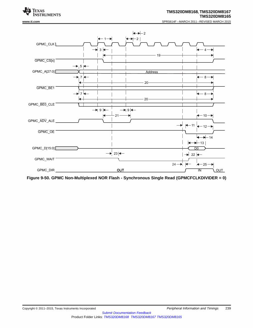
GPMC_CLK
GPMC_CS[x]
GPMC_A[27:0]
GPMC_ _CLEBE0
GPMC_BE1
GPMC_ _ALEADV
GPMC_OE
GPMC_D[15:0]
GPMC_WAIT
GPMC_DIR
Address
D0
OUTOUT IN OUT
1
13
14
7
3
2
2
9
19
11
24
4
5
9
8
21
20
20
10
12
25
7 8
23 22
TMS320DM8168, TMS320DM8167TMS320DM8165
www.ti.com SPRS614F –MARCH 2011–REVISED MARCH 2015
Figure 9-50. GPMC Non-Multiplexed NOR Flash - Synchronous Single Read (GPMCFCLKDIVIDER = 0)
Copyright © 2011–2015, Texas Instruments Incorporated Peripheral Information and Timings 239Submit Documentation Feedback
Product Folder Links: TMS320DM8168 TMS320DM8167 TMS320DM8165

Address
D1 D2
OUT
D0
GPMC_CLK
GPMC_CS[x]
GPMC_A[27:0]
GPMC_ _CLEBE0
GPMC_BE1
GPMC_ _ALEADV
GPMC_WE
GPMC_D[15:0]
GPMC_WAIT
GPMC_DIR
2
3
9
19
4
5
9
21 10
2
7
7
22
D3
1
15
15
23
1818 18
1818 18
16
16 16
Address
Valid
Valid
D1 D2 D3
OUTOUT IN OUT
D0
GPMC_CLK
GPMC_CS[x]
GPMC_A[27:0]
GPMC_ _CLEBE0
GPMC_BE1
GPMC_ _ALEADV
GPMC_OE
GPMC_D[15:0]
GPMC_WAIT
GPMC_DIR
1
13
3
2
9
19
11
4
5
9
8
21
20
10
12
25
8
2
7
720
23
24
14 13
22
TMS320DM8168, TMS320DM8167TMS320DM8165SPRS614F –MARCH 2011–REVISED MARCH 2015 www.ti.com
Figure 9-51. GPMC Non-Multiplexed NOR Flash - 4x16-bit Synchronous Burst Read(GPMCFCLKDIVIDER = 0)
Figure 9-52. GPMC Non-Multiplexed NOR Flash - Synchronous Burst Write (GPMCFCLKDIVIDER = 0)
240 Peripheral Information and Timings Copyright © 2011–2015, Texas Instruments IncorporatedSubmit Documentation Feedback
Product Folder Links: TMS320DM8168 TMS320DM8167 TMS320DM8165

GPMC_CLK
GPMC_CS[x]
GPMC_A[27:16]
GPMC_ _CLEBE0
GPMC_BE1
GPMC_ _ALEADV
GPMC_OE
GPMC_D[15:0]
GPMC_WAIT
GPMC_DIR
Address (MSB)
D0
OUTOUT IN OUT
1
13
14
7
3
2
2
9
19
11
24
4
5
9
8
21
20
20
10
12
25
7 8
23 22
Address (LSB)
5 6
TMS320DM8168, TMS320DM8167TMS320DM8165
www.ti.com SPRS614F –MARCH 2011–REVISED MARCH 2015
Figure 9-53. GPMC Multiplexed NOR Flash - Synchronous Single Read (GPMCFCLKDIVIDER = 0)
Copyright © 2011–2015, Texas Instruments Incorporated Peripheral Information and Timings 241Submit Documentation Feedback
Product Folder Links: TMS320DM8168 TMS320DM8167 TMS320DM8165

Address (MSB)
D1 D2
OUT
D0
GPMC_CLK
GPMC_CS[x]
GPMC_A[27:16]
GPMC_ _CLEBE0
GPMC_BE1
GPMC_ _ALEADV
GPMC_WE
GPMC_D[15:0]
GPMC_WAIT
GPMC_DIR
2
3
9
19
4
5
9
21 10
2
7
7
22
D3
1
15
15
23
1818 18
1818 18
16
16 16Address (LSB)
Address (MSB)
Valid
Valid
D1 D2 D3
OUTOUT IN OUT
D0
GPMC_CLK
GPMC_CS[x]
GPMC_A[27:16]
GPMC_ _CLEBE0
GPMC_BE1
GPMC_ _ALEADV
GPMC_OE
GPMC_D[15:0]
GPMC_WAIT
GPMC_DIR
1
13
3
2
9
19
11
4
5
9
8
21
20
10
12
25
8
2
7
720
23
24
14 13
22
Address (LSB)
65
TMS320DM8168, TMS320DM8167TMS320DM8165SPRS614F –MARCH 2011–REVISED MARCH 2015 www.ti.com
Figure 9-54. GPMC Multiplexed NOR Flash - 4x16-bit Synchronous Burst Read (GPMCFCLKDIVIDER = 0)
Figure 9-55. GPMC Multiplexed NOR Flash - Synchronous Burst Write (GPMCFCLKDIVIDER = 0)
242 Peripheral Information and Timings Copyright © 2011–2015, Texas Instruments IncorporatedSubmit Documentation Feedback
Product Folder Links: TMS320DM8168 TMS320DM8167 TMS320DM8165

TMS320DM8168, TMS320DM8167TMS320DM8165
www.ti.com SPRS614F –MARCH 2011–REVISED MARCH 2015
9.8.2.2 GPMC and NOR Flash Interface Asynchronous Mode Timing
Table 9-56. GPMC and NOR Flash Interface Asynchronous Mode Timing - Internal ParametersNO. MIN MAX UNIT
1 Max. output data generation delay from internal functional clock 6.5 ns2 Max. input data capture delay by internal functional clock 4 ns3 Max. chip select generation delay from internal functional clock 6.5 ns4 Max. address generation delay from internal functional clock 6.5 ns5 Max. address valid generation delay from internal functional clock 6.5 ns6 Max. byte enable generation delay from internal functional clock 6.5 ns7 Max. output enable generation delay from internal functional clock 6.5 ns8 Max. write enable generation delay from internal functional clock 6.5 ns9 Max. functional clock skew 100 ps
Table 9-57. Timing Requirements for GPMC and NOR Flash Interface - Asynchronous Mode(see Figure 9-56, Figure 9-57, Figure 9-58, Figure 9-60)
NO. MIN MAX UNIT6 tacc(DAT) Data maximum access time (GPMC_FCLK cycles) H (1) cycles
Page mode successive data maximum access time (GPMC_FCLK21 tacc1-pgmode(DAT) P (2) cyclescycles)22 tacc2-pgmode(DAT) Page mode first data maximum access time (GPMC_FCLK cycles) H (1) cycles
(1) H = AccessTime * (TimeParaGranularity + 1)(2) P = PageBurstAccessTime * (TimeParaGranularity + 1).
Table 9-58. Switching Characteristics Over Recommended Operating Conditions for GPMC and NORFlash Interface - Asynchronous Mode
(see Figure 9-56, Figure 9-57, Figure 9-58, Figure 9-59, Figure 9-60, Figure 9-61)NO. PARAMETER MIN MAX UNIT
1 tw(nBEV) Pulse duration, GPMC_BE0_CLE, GPMC_BE1 valid time N (1) ns2 tw(nCSV) Pulse duration, GPMC_CS[x] low A (2) ns4 td(nCSV-nADVIV) Delay time, GPMC_CS[x] valid to GPMC_NADV_ALE invalid B - 0.2 (3) B + 2.0 (3) ns
Delay time, GPMC_CS[x] valid to GPMC_OE_RE invalid (single5 td(nCSV-nOEIV) C - 0.2 (4) C + 2.0 (4) nsread)10 td(AV-nCSV) Delay time, address bus valid to GPMC_CS[x] valid J - 0.2 (5) J + 2.0 (5) ns
Delay time, GPMC_BE0_CLE, GPMC_BE1 valid to GPMC_CS[x]11 td(nBEV-nCSV) J - 0.2 (5) J + 2.0 (5) nsvalid13 td(nCSV-nADVV) Delay time, GPMC_CS[x] valid to GPMC_ADV_ALE valid K - 0.2 (6) K + 2.0 (6) ns14 td(nCSV-nOEV) Delay time, GPMC_CS[x] valid to GPMC_OE_RE valid L - 0.2 (7) L + 2.0 (7) ns
(1) For single read: N = RdCycleTime * (TimeParaGranularity + 1) * GPMC_FCLKFor single write: N = WrCycleTime * (TimeParaGranularity + 1) * GPMC_FCLKFor burst read: N = (RdCycleTime + (n - 1) * PageBurstAccessTime) * (TimeParaGranularity + 1) * GPMC_FCLKFor burst write: N = (WrCycleTime + (n - 1) * PageBurstAccessTime) * (TimeParaGranularity + 1) * GPMC_FCLK
(2) For single read: A = (CSRdOffTime - CSOnTime) * (TimeParaGranularity + 1) * GPMC_FCLKFor single write: A = (CSWrOffTime - CSOnTime) * (TimeParaGranularity + 1) * GPMC_FCLKFor burst read: A = (CSRdOffTime - CSOnTime + (n - 1) * PageBurstAccessTime) * (TimeParaGranularity + 1) * GPMC_FCLKFor burst write: A = (CSWrOffTime - CSOnTime + (n - 1) * PageBurstAccessTime) * (TimeParaGranularity + 1) * GPMC_FCLK
(3) = B - nCS Max Delay + nADV Min DelayFor reading: B = ((ADVRdOffTime - CSOnTime) * (TimeParaGranularity + 1) + 0.5 * (ADVExtraDelay - CSExtraDelay)) * GPMC_FCLKFor writing: B = ((ADVWrOffTime - CSOnTime) * (TimeParaGranularity + 1) + 0.5 * (ADVExtraDelay - CSExtraDelay)) * GPMC_FCLK
(4) = C - nCS Max Delay + nOE Min DelayC = ((OEOffTime - CSOnTime) * (TimeParaGranularity + 1) + 0.5 * (OEExtraDelay - CSExtraDelay)) * GPMC_FCLK
(5) = J - Address Max Delay + nCS Min DelayJ = (CSOnTime * (TimeParaGranularity + 1) + 0.5 * CSExtraDelay) * GPMC_FCLK
(6) = K - nCS Max Delay + nADV Min DelayK = ((ADVOnTime - CSOnTime) * (TimeParaGranularity + 1) + 0.5 * (ADVExtraDelay - CSExtraDelay)) * GPMC_FCLK
(7) = L - nCS Max Delay + nOE Min DelayL = ((OEOnTime - CSOnTime) * (TimeParaGranularity + 1) + 0.5 * (OEExtraDelay - CSExtraDelay)) * GPMC_FCLK
Copyright © 2011–2015, Texas Instruments Incorporated Peripheral Information and Timings 243Submit Documentation Feedback
Product Folder Links: TMS320DM8168 TMS320DM8167 TMS320DM8165

TMS320DM8168, TMS320DM8167TMS320DM8165SPRS614F –MARCH 2011–REVISED MARCH 2015 www.ti.com
Table 9-58. Switching Characteristics Over Recommended Operating Conditions for GPMC and NORFlash Interface - Asynchronous Mode (continued)
(see Figure 9-56, Figure 9-57, Figure 9-58, Figure 9-59, Figure 9-60, Figure 9-61)NO. PARAMETER MIN MAX UNIT15 td(nCSV-DIR) Delay time, GPMC_CS[x] valid to GPMC_DIR high L - 0.2 (7) L + 2.0 (7) ns16 td(nCSV-DIR) Delay time, GPMC_CS[x] valid to GPMC_DIR low M - 0.2 (8) M + 2.0 (8) ns
Address invalid duration between 2 successive read or write17 tw(AIV) G (9) nsaccessesDelay time, GPMC_CS[x] valid to GPMC_OE_RE invalid (burst19 td(nCSV-nOEIV) I - 0.2 (10) I + 2.0 (10) nsread)
21 tw(AV) Pulse duration, address valid: second, third and fourth accesses D (11) ns26 td(nCSV-nWEV) Delay time, GPMC_CS[x] valid to GPMC_WE valid E - 0.2 (12) E + 2.0 (12) ns28 td(nCSV-nWEIV) Delay time, GPMC_CS[x] valid to GPMC_WE invalid F - 0.2 (13) F + 2.0 (13) ns29 td(nWEV-DV) Delay time, GPMC_WE valid to data bus valid 2.0 ns30 td(DV-nCSV) Delay time, data bus valid to GPMC_CS[x] valid J - 0.2 (5) J + 2.0 (5) ns
Delay time, GPMC_OE_RE valid to GPMC_A[16:1]_D[15:0]38 td(nOEV-AIV) 2.0 nsaddress phase end
(8) = M - nCS Max Delay + nOE Min DelayM = ((RdCycleTime - CSOnTime) * (TimeParaGranularity + 1) - 0.5 * CSExtraDelay) * GPMC_FCLK.Parameter M expression is given as one example of GPMC programming. The IO DIR signal goes from IN to OUT after bothRdCycleTime and BusTurnAround completion. Behavior of the IO direction signal depends on the kind of successive read and writeaccesses performed to the memory and multiplexed or non-multiplexed memory addressing scheme, whether the bus keeping feature isenabled or not. The IO DIR behavior is automatically handled by the GPMC controller.
(9) G = Cycle2CycleDelay * GPMC_FCLK(10) = I - nCS Max Delay + nOE Min Delay
I = ((OEOffTime + (n - 1) * PageBurstAccessTime - CSOnTime) * (TimeParaGranularity + 1) + 0.5 * (OEExtraDelay - CSExtraDelay)) *GPMC_FCLK
(11) D = PageBurstAccessTime * (TimeParaGranularity + 1) * GPMC_FCLK(12) = E - nCS Max Delay + nWE Min Delay
E = ((WEOnTime - CSOnTime) * (TimeParaGranularity + 1) + 0.5 * (WEExtraDelay - CSExtraDelay)) * GPMC_FCLK(13) = F - nCS Max Delay + nWE Min Delay
F = ((WEOffTime - CSOnTime) * (TimeParaGranularity + 1) + 0.5 * (WEExtraDelay - CSExtraDelay)) * GPMC_FCLK
244 Peripheral Information and Timings Copyright © 2011–2015, Texas Instruments IncorporatedSubmit Documentation Feedback
Product Folder Links: TMS320DM8168 TMS320DM8167 TMS320DM8165
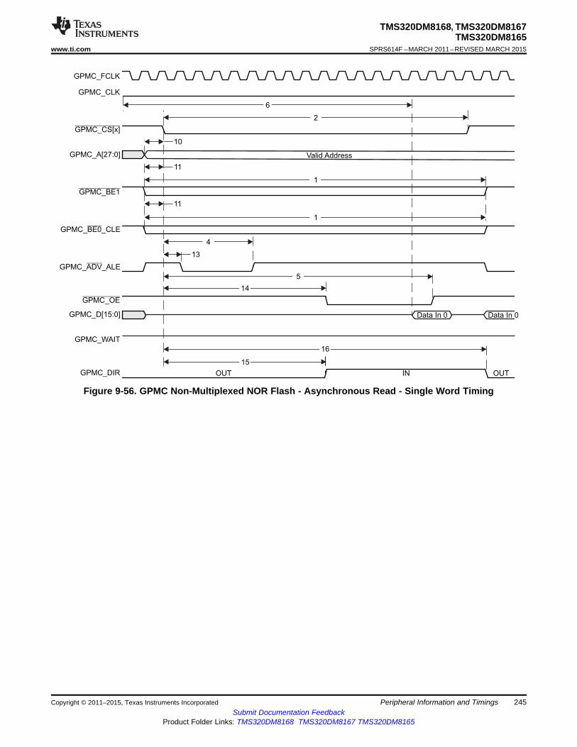
GPMC_CLK
GPMC_CS[x]
GPMC_A[ ]27:0
GPMC_ _CLEBE0
GPMC_BE1
GPMC_ _ALEADV
GPMC_OE
GPMC_D[15:0]
GPMC_WAIT
GPMC_DIR
Valid Address
OUT IN OUT
2
6
10
4
1
1
GPMC_FCLK
Data In 0
11
11
13
5
14
15
16
Data In 0
TMS320DM8168, TMS320DM8167TMS320DM8165
www.ti.com SPRS614F –MARCH 2011–REVISED MARCH 2015
Figure 9-56. GPMC Non-Multiplexed NOR Flash - Asynchronous Read - Single Word Timing
Copyright © 2011–2015, Texas Instruments Incorporated Peripheral Information and Timings 245Submit Documentation Feedback
Product Folder Links: TMS320DM8168 TMS320DM8167 TMS320DM8165
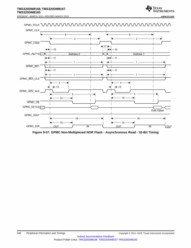
GPMC_CLK
GPMC_CS[x]
GPMC_A[ ]27:0
GPMC_ _CLEBE0
GPMC_BE1
GPMC_ _ALEADV
GPMC_OE
GPMC_D[15:0]
GPMC_WAIT
GPMC_DIR
Address 1
OUT IN OUT
2
6
10
4
1
GPMC_FCLK
Data Upper
11
11
13
5
14
15
16
Address 2
OUT IN
6
2
1
1 1
17
10
11
11
4
13
5
14
15
16
TMS320DM8168, TMS320DM8167TMS320DM8165SPRS614F –MARCH 2011–REVISED MARCH 2015 www.ti.com
Figure 9-57. GPMC Non-Multiplexed NOR Flash - Asynchronous Read - 32-Bit Timing
246 Peripheral Information and Timings Copyright © 2011–2015, Texas Instruments IncorporatedSubmit Documentation Feedback
Product Folder Links: TMS320DM8168 TMS320DM8167 TMS320DM8165

GPMC_CLK
GPMC_CS[x]
GPMC_A[27:0]
GPMC_ _CLEBE0
GPMC_BE1
GPMC_ _ALEADV
GPMC_OE
GPMC_D[15:0]
GPMC_WAIT
GPMC_DIR
Add0
OUT IN OUT
2
22
10
1
1
GPMC_FCLK
D0
11
11
13
19
14
15
16
D3
Add1 Add2 Add3 Add4
D1 D2 D3
2121
21
TMS320DM8168, TMS320DM8167TMS320DM8165
www.ti.com SPRS614F –MARCH 2011–REVISED MARCH 2015
Figure 9-58. GPMC Non-Multiplexed Only NOR Flash - Asynchronous Read - Page Mode 4x16-Bit Timing
Copyright © 2011–2015, Texas Instruments Incorporated Peripheral Information and Timings 247Submit Documentation Feedback
Product Folder Links: TMS320DM8168 TMS320DM8167 TMS320DM8165
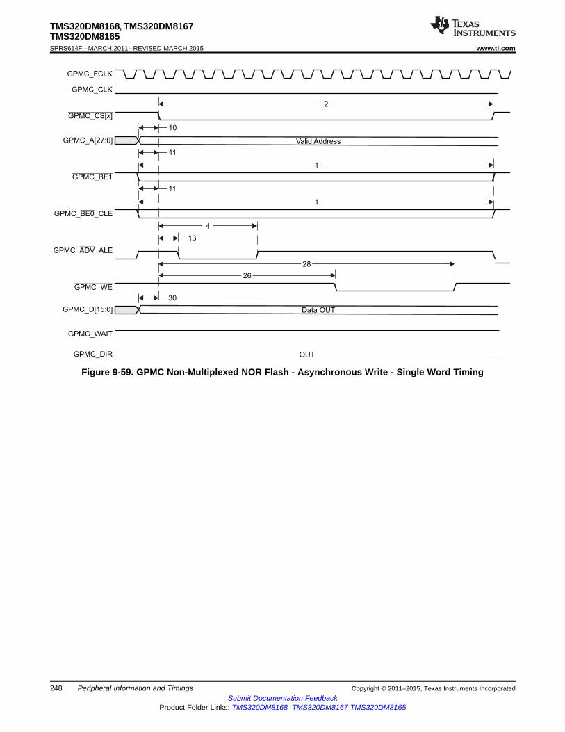
GPMC_CLK
GPMC_CS[x]
GPMC_A[ ]27:0
GPMC_ _CLEBE0
GPMC_BE1
GPMC_ _ALEADV
GPMC_WE
GPMC_D[15:0]
GPMC_WAIT
GPMC_DIR
Valid Address
OUT
2
10
4
1
1
GPMC_FCLK
11
11
13
28
26
Data OUT
30
TMS320DM8168, TMS320DM8167TMS320DM8165SPRS614F –MARCH 2011–REVISED MARCH 2015 www.ti.com
Figure 9-59. GPMC Non-Multiplexed NOR Flash - Asynchronous Write - Single Word Timing
248 Peripheral Information and Timings Copyright © 2011–2015, Texas Instruments IncorporatedSubmit Documentation Feedback
Product Folder Links: TMS320DM8168 TMS320DM8167 TMS320DM8165
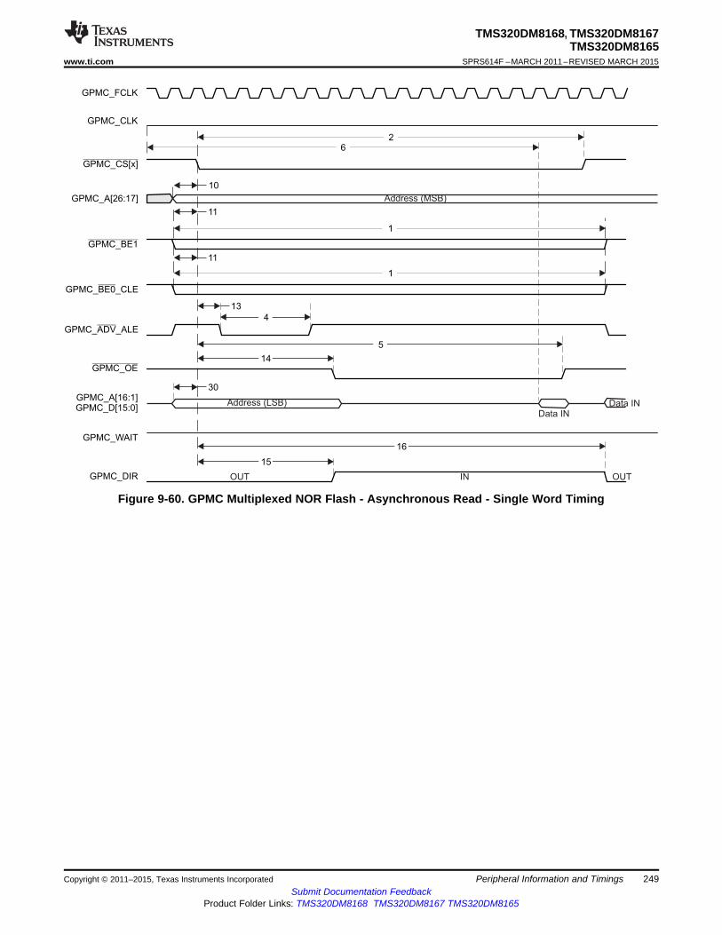
Address (MSB)
IN
GPMC_CLK
GPMC_CS[x]
GPMC_A[26:17]
GPMC_ _CLEBE0
GPMC_BE1
GPMC_ _ALEADV
GPMC_OE
GPMC_A[16:1]GPMC_D[15:0]
GPMC_WAIT
GPMC_DIR
2
10
4
11
11
Data INAddress (LSB)
GPMC_FCLK
Data IN
OUTOUT
6
1
1
13
14
5
30
15
16
TMS320DM8168, TMS320DM8167TMS320DM8165
www.ti.com SPRS614F –MARCH 2011–REVISED MARCH 2015
Figure 9-60. GPMC Multiplexed NOR Flash - Asynchronous Read - Single Word Timing
Copyright © 2011–2015, Texas Instruments Incorporated Peripheral Information and Timings 249Submit Documentation Feedback
Product Folder Links: TMS320DM8168 TMS320DM8167 TMS320DM8165

Address (MSB)
GPMC_CLK
GPMC_CS[x]
GPMC_A[26:17]
GPMC_ _CLEBE0
GPMC_BE1
GPMC_ _ALEADV
GPMC_WE
GPMCA[16:1]GPMC_D[15:0]
GPMC_WAIT
GPMC_DIR
2
10
4
11
11
Data OUTValid Address (LSB)
GPMC_FCLK
OUT
1
1
13
26
28
30 29
TMS320DM8168, TMS320DM8167TMS320DM8165SPRS614F –MARCH 2011–REVISED MARCH 2015 www.ti.com
Figure 9-61. GPMC Multiplexed NOR Flash - Asynchronous Write - Single Word Timing
250 Peripheral Information and Timings Copyright © 2011–2015, Texas Instruments IncorporatedSubmit Documentation Feedback
Product Folder Links: TMS320DM8168 TMS320DM8167 TMS320DM8165
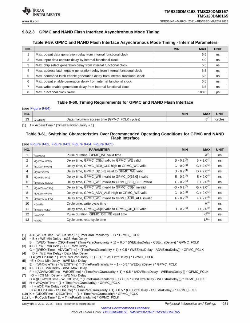
TMS320DM8168, TMS320DM8167TMS320DM8165
www.ti.com SPRS614F –MARCH 2011–REVISED MARCH 2015
9.8.2.3 GPMC and NAND Flash Interface Asynchronous Mode Timing
Table 9-59. GPMC and NAND Flash Interface Asynchronous Mode Timing - Internal ParametersNO. MIN MAX UNIT
1 Max. output data generation delay from internal functional clock 6.5 ns2 Max. input data capture delay by internal functional clock 4.0 ns3 Max. chip select generation delay from internal functional clock 6.5 ns4 Max. address latch enable generation delay from internal functional clock 6.5 ns5 Max. command latch enable generation delay from internal functional clock 6.5 ns6 Max. output enable generation delay from internal functional clock 6.5 ns7 Max. write enable generation delay from internal functional clock 6.5 ns8 Max. functional clock skew 100.0 ps
Table 9-60. Timing Requirements for GPMC and NAND Flash Interface(see Figure 9-64)
NO. MIN MAX UNIT13 tacc(DAT) Data maximum access time (GPMC_FCLK cycles) J (1) cycles
(1) J = AccessTime * (TimeParaGranularity + 1)
Table 9-61. Switching Characteristics Over Recommended Operating Conditions for GPMC and NANDFlash Interface
(see Figure 9-62, Figure 9-63, Figure 9-64, Figure 9-65)NO. PARAMETER MIN MAX UNIT
1 tw(nWEV) Pulse duration, GPMC_WE valid time A (1) ns2 td(nCSV-nWEV) Delay time, GPMC_CS[x] valid to GPMC_WE valid B - 0.2 (2) B + 2.0 (2) ns3 td(CLEH-nWEV) Delay time, GPMC_BE0_CLE high to GPMC_WE valid C - 0.2 (3) C + 2.0 (3) ns4 td(nWEV-DV) Delay time, GPMC_D[15:0] valid to GPMC_WE valid D - 0.2 (4) D + 2.0 (4) ns5 td(nWEIV-DIV) Delay time, GPMC_WE invalid to GPMC_D[15:0] invalid E - 0.2 (5) E + 2.0 (5) ns6 td(nWEIV-CLEIV) Delay time, GPMC_WE invalid to GPMC_BE0_CLE invalid F - 0.2 (6) F + 2.0 (6) ns7 td(nWEIV-nCSIV) Delay time, GPMC_WE invalid to GPMC_CS[x] invalid G - 0.2 (7) G + 2.0 (7) ns8 td(ALEH-nWEV) Delay time, GPMC_ADV_ALE High to GPMC_WE valid C - 0.2 (3) C + 2.0 (3) ns9 td(nWEIV-ALEIV) Delay time, GPMC_WE invalid to GPMC_ADV_ALE invalid F - 0.2 (6) F + 2.0 (6) ns10 tc(nWE) Cycle time, write cycle time H (8) ns11 td(nCSV-nOEV) Delay time, GPMC_CS[x] valid to GPMC_OE_RE valid I - 0.2 (9) I + 2.0 (9) ns12 tw(nOEV) Pulse duration, GPMC_OE_RE valid time K (10) ns13 tc(nOE) Cycle time, read cycle time L (11) ns
(1) A = (WEOffTime - WEOnTime) * (TimeParaGranularity + 1) * GPMC_FCLK(2) = B + nWE Min Delay - nCS Max Delay
B = ((WEOnTime - CSOnTime) * (TimeParaGranularity + 1) + 0.5 * (WEExtraDelay - CSExtraDelay)) * GPMC_FCLK(3) = C + nWE Min Delay - CLE Max Delay
C = ((WEOnTime - ADVOnTime) * (TimeParaGranularity + 1) + 0.5 * (WEExtraDelay - ADVExtraDelay)) * GPMC_FCLK(4) = D + nWE Min Delay - Data Max Delay
D = (WEOnTime * (TimeParaGranularity + 1) + 0.5 * WEExtraDelay ) * GPMC_FCLK(5) =E + Data Min Delay - nWE Max Delay
E = ((WrCycleTime - WEOffTime) * (TimeParaGranularity + 1) - 0.5 * WEExtraDelay ) * GPMC_FCLK(6) = F + CLE Min Delay - nWE Max Delay
F = ((ADVWrOffTime - WEOffTime) * (TimeParaGranularity + 1) + 0.5 * (ADVExtraDelay - WEExtraDelay )) * GPMC_FCLK(7) =G + nCS Min Delay - nWE Max Delay
G = ((CSWrOffTime - WEOffTime) * (TimeParaGranularity + 1) + 0.5 * (CSExtraDelay - WEExtraDelay )) * GPMC_FCLK(8) H = WrCycleTime * (1 + TimeParaGranularity) * GPMC_FCLK(9) = I + nOE Min Delay - nCS Max Delay
I = ((OEOnTime - CSOnTime) * (TimeParaGranularity + 1) + 0.5 * (OEExtraDelay - CSExtraDelay)) * GPMC_FCLK(10) K = (OEOffTime - OEOnTime) * (1 + TimeParaGranularity) * GPMC_FCLK(11) L = RdCycleTime * (1 + TimeParaGranularity) * GPMC_FCLK
Copyright © 2011–2015, Texas Instruments Incorporated Peripheral Information and Timings 251Submit Documentation Feedback
Product Folder Links: TMS320DM8168 TMS320DM8167 TMS320DM8165

GPMC_FCLK
GPMC_CS[x]
GPMC_ _CLEBE0
GPMC_ _ALEADV
GPMC_OE
GPMC_WE
GPMC_A[16:1]GPMC_D[15:0]
27
9
1
5
8
10
4
Address
GPMC_FCLK
GPMC_CS[x]
GPMC_ _CLEBE0
GPMC_ _ALEADV
GPMC_OE
GPMC_WE
GPMC_A[16:1]GPMC_D[15:0]
2
3
7
6
1
4 5
Command
TMS320DM8168, TMS320DM8167TMS320DM8165SPRS614F –MARCH 2011–REVISED MARCH 2015 www.ti.com
Table 9-61. Switching Characteristics Over Recommended Operating Conditions for GPMC and NANDFlash Interface (continued)
(see Figure 9-62, Figure 9-63, Figure 9-64, Figure 9-65)NO. PARAMETER MIN MAX UNIT14 td(nOEIV-nCSIV) Delay time, GPMC_OE_RE invalid to GPMC_CS[x] invalid M - 0.2 (12) M + 2.0 (12) ns
(12) =M + nCS Min Delay - nOE Max DelayM = ((CSRdOffTime - OEOffTime) * (TimeParaGranularity + 1) + 0.5 * (CSExtraDelay - OEExtraDelay ))* GPMC_FCLK
Figure 9-62. GPMC and NAND Flash - Command Latch Cycle Timing
Figure 9-63. GPMC and NAND Flash - Address Latch Cycle Timing
252 Peripheral Information and Timings Copyright © 2011–2015, Texas Instruments IncorporatedSubmit Documentation Feedback
Product Folder Links: TMS320DM8168 TMS320DM8167 TMS320DM8165

GPMC_FCLK
GPMC_CS[x]
GPMC_ _CLEBE0
GPMC_ _ALEADV
GPMC_WE
GPMC_A[16:1]GPMC_D[15:0]
2
10
Data
1
7
GPMC_OE
4 5
GPMC_FCLK
GPMC_CS[x]
GPMC_ _CLEBE0
GPMC_ _ALEADV
GPMC_OE
GPMC_A[16:1]GPMC_D[15:0]
13
1611
15
Data
GPMC_WAIT
14
TMS320DM8168, TMS320DM8167TMS320DM8165
www.ti.com SPRS614F –MARCH 2011–REVISED MARCH 2015
Figure 9-64. GPMC and NAND Flash - Data Read Cycle Timing
Figure 9-65. GPMC and NAND Flash - Data Write Cycle Timing
Copyright © 2011–2015, Texas Instruments Incorporated Peripheral Information and Timings 253Submit Documentation Feedback
Product Folder Links: TMS320DM8168 TMS320DM8167 TMS320DM8165
TMS320DM8168, TMS320DM8167TMS320DM8165SPRS614F –MARCH 2011–REVISED MARCH 2015 www.ti.com
9.9 High-Definition Multimedia Interface (HDMI)The device includes an HDMI 1.3a-compliant transmitter for digital video and audio data to displaydevices. The HDMI interface consists of a digital HDMI transmitter core with TMDS encoder, a corewrapper with interface logic and control registers, and a transmit PHY, with the following features:• Hot-plug detection• Consumer electronics control (CEC) messages• DVI 1.0 compliant (only RGB pixel format)• CEA 861-D and VESA DMT formats• Supports up to 165-MHz pixel clock:
– 1920 x 1080p @75 Hz with 8-bit component color depth– 1920 x 1200 @60 Hz with 8-bit component color depth– 1600 x 1200 @60 Hz with 8-bit component color depth
• Support for deep-color mode:– 10-bit component color depth up to 1080p @60 Hz (maximum pixel clock = 148.5 MHz)– 12-bit component color depth at 720p or 1080i @60 Hz (maximum pixel clock = 123.75 MHz)
• Uncompressed multichannel (up to eight channels) audio (L-PCM) support• Master I2C interface for display data channel (DDC) connection• TMDS clock to the HDMI-PHY is up to 185.625 MHz• Maximum supported pixel clock:
– 165 MHz for 8-bit color depth– 148.5 MHz for 10-bit color depth– 123.75 MHz for 12-bit color depth
• Options available to support HDCP encryption engine for transmitting protected audio and video(contact local TI sales representative for information).
For more details on the HDMI, see the HDMI chapter in the TMS320DM816x DaVinci Digital MediaProcessors Technical Reference Manual (literature number SPRUGX8).
9.9.1 HDMI Interface Design Specifications
NOTEFor more information on PCB layout, see the DM816xx Easy CYG Package PCB EscapeRouting application report (literature number SPRABK6).
This section provides PCB design and layout specifications for the HDMI interface. The design rulesconstrain PCB trace length, PCB trace skew, signal integrity, cross-talk, and signal timing. Simulation andsystem design work has been done to ensure the HDMI interface requirements are met.
9.9.1.1 HDMI Interface Schematic
The HDMI bus is separated into three main sections:1. Transition Minimized Differential Signaling (TMDS) high-speed digital video interface2. Display Data Channel (I2C bus for configuration and status exchange between two devices)3. Consumer Electronics Control (optional) for remote control of connected devices.
The DDC and CEC are low-speed interfaces, so nothing special is required for PCB layout of thesesignals. Their connection is shown in Figure 9-66.
The TMDS channels are high-speed differential pairs and, therefore, require the most care in layout.Specifications for TMDS layout are below.
254 Peripheral Information and Timings Copyright © 2011–2015, Texas Instruments IncorporatedSubmit Documentation Feedback
Product Folder Links: TMS320DM8168 TMS320DM8167 TMS320DM8165

TD0+
TD0-
TD1+
TD1-
TD2+
TD2-
TD0Shld
TD1Shld
TD2Shld
TCLKShld
CEC
SDA
SCL
DDCGnd
Rpullup(A)
DVDD_3P3
HDMI_TMDSDP0
HDMI_TMDSDN0
HDMI_TMDSDP1
HDMI_TMDSDN1
HDMI_TMDSDN2
HDMI_TMDSDP2
HDMI_TMDSCLKP
HDMI_TMDSCLKN
HDMI_CEC
HDMI_SDA
HDMI_SCL
HDMI ConnectorDevice
TCLK+
TCLK
TPD12S521or other
ESD Protectionw/I2C-LevelTranslation
HPDETHDMI_HPDET
TMS320DM8168, TMS320DM8167TMS320DM8165
www.ti.com SPRS614F –MARCH 2011–REVISED MARCH 2015
Figure 9-66 shows the HDMI interface schematic. The specific pin numbers can be obtained from Table 4-7, HDMI Terminal Functions.
A. 5K-10K Ω pullup resistors are required if not integrated in the ESD protection chip.
Figure 9-66. HDMI Interface High-Level Schematic
9.9.1.2 TMDS Routing
The TMDS signals are high-speed differential pairs. Care must be taken in the PCB layout of these signalsto ensure good signal integrity.
The TMDS differential signal traces must be routed to achieve 100 Ω (±10%) differential impedance and60 Ω (±10%) single-ended impedance. Single-ended impedance control is required because differentialsignals are extremely difficult to closely couple on PCBs and, therefore, single-ended impedance becomesimportant.
These impedances are impacted by trace width, trace spacing, distance to reference planes, and dielectricmaterial. Verify with a PCB design tool that the trace geometry for both data signal pairs results in asclose to 60 Ω impedance traces as possible. For best accuracy, work with your PCB fabricator to ensurethis impedance is met.
In general, closely coupled differential signal traces are not an advantage on PCBs. When differentialsignals are closely coupled, tight spacing and width control is necessary. Very small width and spacingvariations affect impedance dramatically, so tight impedance control can be more problematic to maintainin production.
Loosely coupled PCB differential signals make impedance control much easier. Wider traces and spacingmake obstacle avoidance easier, and trace width variations do not affect impedance as much; therefore, itis easier to maintain an accurate impedance over the length of the signal. The wider traces also showreduced skin effect and, therefore, often result in better signal integrity.
Table 9-62 shows the routing specifications for the TMDS signals.
Copyright © 2011–2015, Texas Instruments Incorporated Peripheral Information and Timings 255Submit Documentation Feedback
Product Folder Links: TMS320DM8168 TMS320DM8167 TMS320DM8165

TMS320DM8168, TMS320DM8167TMS320DM8165SPRS614F –MARCH 2011–REVISED MARCH 2015 www.ti.com
Table 9-62. TMDS Routing Specifications
PARAMETER MIN TYP MAX UNITProcessor-to-HDMI header trace length 7000 MilsNumber of stubs allowed on TMDS traces 0 StubsTX and RX pair differential impedance 90 100 110 ΩTX and RX single-ended impedance 54 60 66 ΩNumber of vias on each TMDS trace 2 Vias (1)
TMDS differential pair to any other trace spacing 2*DS (2)
(1) Vias must be used in pairs with their distance minimized.(2) DS = differential spacing of the HDMI traces.
9.9.1.3 DDC Signals
As shown in Figure 9-66, the DDC connects just like a standard I2C bus. As such, resistor pullups mustbe used to pull up the open drain buffer signals unless they are integrated into the ESD protection chipused. If used, these pullup resistors should be connected to a 3.3-V supply.
9.9.1.4 HDMI ESD Protection Device (Required)
Interfaces that connect to a cable such as HDMI generally require more ESD protection than can be builtinto the processor's outputs. Therefore, this HDMI interface requires the use of an ESD protection chip toprovide adequate ESD protection and to translate I2C voltage levels from the 3.3 V supplied by the deviceto the 5 volts required by the HDMI specification.
When selecting an ESD protection chip, choose the lowest capacitance ESD protection available tominimize signal degradation. In no case should the ESD protection circuit capacitance be more than 5 pF.
TI manufactures devices that provide ESD protection for HDMI signals such as the TPD12S521. For moreinformation see the www.ti.com website.
9.9.1.5 PCB Stackup Specifications
Table 9-63 shows the stackup and feature sizes required for HDMI.
Table 9-63. HDMI PCB Stackup Specifications
PARAMETER MIN TYP MAX UNITPCB routing and plane layers 4 6 - LayersSignal routing layers 2 3 - LayersNumber of ground plane cuts allowed within HDMI routing region - - 0 CutsNumber of layers between HDMI routing region and reference ground plane - - 0 LayersPCB trace width - 4 - MilsPCB BGA escape via pad size - 20 - MilsPCB BGA escape via hole size - 10 MilsProcessor device BGA pad size (1) (2) 0.3 mm
(1) Non-solder mask defined pad.(2) Per IPC-7351A BGA pad size guideline.
256 Peripheral Information and Timings Copyright © 2011–2015, Texas Instruments IncorporatedSubmit Documentation Feedback
Product Folder Links: TMS320DM8168 TMS320DM8167 TMS320DM8165
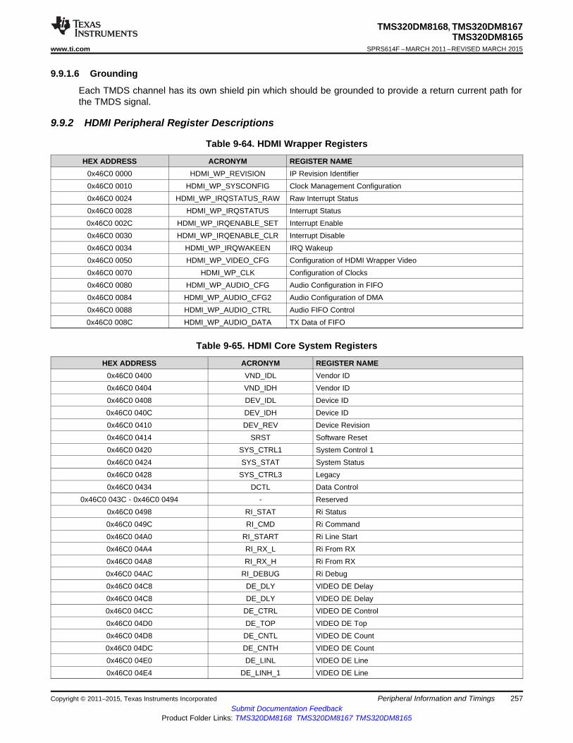
TMS320DM8168, TMS320DM8167TMS320DM8165
www.ti.com SPRS614F –MARCH 2011–REVISED MARCH 2015
9.9.1.6 Grounding
Each TMDS channel has its own shield pin which should be grounded to provide a return current path forthe TMDS signal.
9.9.2 HDMI Peripheral Register Descriptions
Table 9-64. HDMI Wrapper Registers
HEX ADDRESS ACRONYM REGISTER NAME0x46C0 0000 HDMI_WP_REVISION IP Revision Identifier0x46C0 0010 HDMI_WP_SYSCONFIG Clock Management Configuration0x46C0 0024 HDMI_WP_IRQSTATUS_RAW Raw Interrupt Status0x46C0 0028 HDMI_WP_IRQSTATUS Interrupt Status0x46C0 002C HDMI_WP_IRQENABLE_SET Interrupt Enable0x46C0 0030 HDMI_WP_IRQENABLE_CLR Interrupt Disable0x46C0 0034 HDMI_WP_IRQWAKEEN IRQ Wakeup0x46C0 0050 HDMI_WP_VIDEO_CFG Configuration of HDMI Wrapper Video0x46C0 0070 HDMI_WP_CLK Configuration of Clocks0x46C0 0080 HDMI_WP_AUDIO_CFG Audio Configuration in FIFO0x46C0 0084 HDMI_WP_AUDIO_CFG2 Audio Configuration of DMA0x46C0 0088 HDMI_WP_AUDIO_CTRL Audio FIFO Control0x46C0 008C HDMI_WP_AUDIO_DATA TX Data of FIFO
Table 9-65. HDMI Core System Registers
HEX ADDRESS ACRONYM REGISTER NAME0x46C0 0400 VND_IDL Vendor ID0x46C0 0404 VND_IDH Vendor ID0x46C0 0408 DEV_IDL Device ID0x46C0 040C DEV_IDH Device ID0x46C0 0410 DEV_REV Device Revision0x46C0 0414 SRST Software Reset0x46C0 0420 SYS_CTRL1 System Control 10x46C0 0424 SYS_STAT System Status0x46C0 0428 SYS_CTRL3 Legacy0x46C0 0434 DCTL Data Control
0x46C0 043C - 0x46C0 0494 - Reserved0x46C0 0498 RI_STAT Ri Status0x46C0 049C RI_CMD Ri Command0x46C0 04A0 RI_START Ri Line Start0x46C0 04A4 RI_RX_L Ri From RX0x46C0 04A8 RI_RX_H Ri From RX0x46C0 04AC RI_DEBUG Ri Debug0x46C0 04C8 DE_DLY VIDEO DE Delay0x46C0 04C8 DE_DLY VIDEO DE Delay0x46C0 04CC DE_CTRL VIDEO DE Control0x46C0 04D0 DE_TOP VIDEO DE Top0x46C0 04D8 DE_CNTL VIDEO DE Count0x46C0 04DC DE_CNTH VIDEO DE Count0x46C0 04E0 DE_LINL VIDEO DE Line0x46C0 04E4 DE_LINH_1 VIDEO DE Line
Copyright © 2011–2015, Texas Instruments Incorporated Peripheral Information and Timings 257Submit Documentation Feedback
Product Folder Links: TMS320DM8168 TMS320DM8167 TMS320DM8165
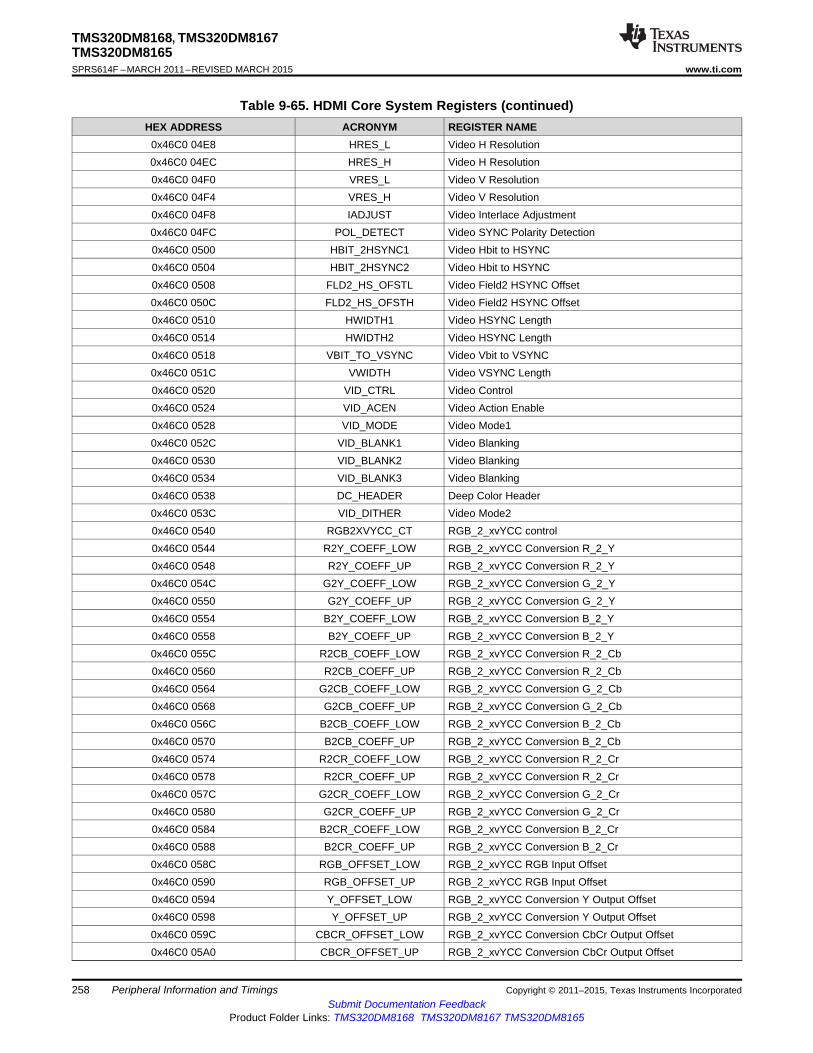
TMS320DM8168, TMS320DM8167TMS320DM8165SPRS614F –MARCH 2011–REVISED MARCH 2015 www.ti.com
Table 9-65. HDMI Core System Registers (continued)HEX ADDRESS ACRONYM REGISTER NAME
0x46C0 04E8 HRES_L Video H Resolution0x46C0 04EC HRES_H Video H Resolution0x46C0 04F0 VRES_L Video V Resolution0x46C0 04F4 VRES_H Video V Resolution0x46C0 04F8 IADJUST Video Interlace Adjustment0x46C0 04FC POL_DETECT Video SYNC Polarity Detection0x46C0 0500 HBIT_2HSYNC1 Video Hbit to HSYNC0x46C0 0504 HBIT_2HSYNC2 Video Hbit to HSYNC0x46C0 0508 FLD2_HS_OFSTL Video Field2 HSYNC Offset0x46C0 050C FLD2_HS_OFSTH Video Field2 HSYNC Offset0x46C0 0510 HWIDTH1 Video HSYNC Length0x46C0 0514 HWIDTH2 Video HSYNC Length0x46C0 0518 VBIT_TO_VSYNC Video Vbit to VSYNC0x46C0 051C VWIDTH Video VSYNC Length0x46C0 0520 VID_CTRL Video Control0x46C0 0524 VID_ACEN Video Action Enable0x46C0 0528 VID_MODE Video Mode10x46C0 052C VID_BLANK1 Video Blanking0x46C0 0530 VID_BLANK2 Video Blanking0x46C0 0534 VID_BLANK3 Video Blanking0x46C0 0538 DC_HEADER Deep Color Header0x46C0 053C VID_DITHER Video Mode20x46C0 0540 RGB2XVYCC_CT RGB_2_xvYCC control0x46C0 0544 R2Y_COEFF_LOW RGB_2_xvYCC Conversion R_2_Y0x46C0 0548 R2Y_COEFF_UP RGB_2_xvYCC Conversion R_2_Y0x46C0 054C G2Y_COEFF_LOW RGB_2_xvYCC Conversion G_2_Y0x46C0 0550 G2Y_COEFF_UP RGB_2_xvYCC Conversion G_2_Y0x46C0 0554 B2Y_COEFF_LOW RGB_2_xvYCC Conversion B_2_Y0x46C0 0558 B2Y_COEFF_UP RGB_2_xvYCC Conversion B_2_Y0x46C0 055C R2CB_COEFF_LOW RGB_2_xvYCC Conversion R_2_Cb0x46C0 0560 R2CB_COEFF_UP RGB_2_xvYCC Conversion R_2_Cb0x46C0 0564 G2CB_COEFF_LOW RGB_2_xvYCC Conversion G_2_Cb0x46C0 0568 G2CB_COEFF_UP RGB_2_xvYCC Conversion G_2_Cb0x46C0 056C B2CB_COEFF_LOW RGB_2_xvYCC Conversion B_2_Cb0x46C0 0570 B2CB_COEFF_UP RGB_2_xvYCC Conversion B_2_Cb0x46C0 0574 R2CR_COEFF_LOW RGB_2_xvYCC Conversion R_2_Cr0x46C0 0578 R2CR_COEFF_UP RGB_2_xvYCC Conversion R_2_Cr0x46C0 057C G2CR_COEFF_LOW RGB_2_xvYCC Conversion G_2_Cr0x46C0 0580 G2CR_COEFF_UP RGB_2_xvYCC Conversion G_2_Cr0x46C0 0584 B2CR_COEFF_LOW RGB_2_xvYCC Conversion B_2_Cr0x46C0 0588 B2CR_COEFF_UP RGB_2_xvYCC Conversion B_2_Cr0x46C0 058C RGB_OFFSET_LOW RGB_2_xvYCC RGB Input Offset0x46C0 0590 RGB_OFFSET_UP RGB_2_xvYCC RGB Input Offset0x46C0 0594 Y_OFFSET_LOW RGB_2_xvYCC Conversion Y Output Offset0x46C0 0598 Y_OFFSET_UP RGB_2_xvYCC Conversion Y Output Offset0x46C0 059C CBCR_OFFSET_LOW RGB_2_xvYCC Conversion CbCr Output Offset0x46C0 05A0 CBCR_OFFSET_UP RGB_2_xvYCC Conversion CbCr Output Offset
258 Peripheral Information and Timings Copyright © 2011–2015, Texas Instruments IncorporatedSubmit Documentation Feedback
Product Folder Links: TMS320DM8168 TMS320DM8167 TMS320DM8165

TMS320DM8168, TMS320DM8167TMS320DM8165
www.ti.com SPRS614F –MARCH 2011–REVISED MARCH 2015
Table 9-65. HDMI Core System Registers (continued)HEX ADDRESS ACRONYM REGISTER NAME0x46C0 05C0 INTR_STATE Interrupt State0x46C0 05C4 INTR1 Interrupt Source0x46C0 05C8 INTR2 Interrupt Source0x46C0 05CC INTR3 Interrupt Source0x46C0 05D0 INTR4 Interrupt Source0x46C0 05D4 INT_UNMASK1 Interrupt Unmask0x46C0 05D8 INT_UNMASK2 Interrupt Unmask0x46C0 05DC INT_UNMASK3 Interrupt Unmask0x46C0 05E0 INT_UNMASK4 Interrupt Unmask0x46C0 05E4 INT_CTRL Interrupt Control0x46C0 0640 XVYCC2RGB_CTL xvYCC_2_RGB Control0x46C0 0644 Y2R_COEFF_LOW xvYCC_2_RGB Conversion Y_2_R0x46C0 0648 Y2R_COEFF_UP xvYCC_2_RGB Conversion Y_2_R0x46C0 064C CR2R_COEFF_LOW xvYCC_2_RGB Conversion Cr_2_R0x46C0 0650 CR2R_COEFF_UP xvYCC_2_RGB Conversion Cr_2_R0x46C0 0654 CB2B_COEFF_LOW xvYCC_2_RGB Conversion Cb_2_B0x46C0 0658 CB2B_COEFF_UP xvYCC_2_RGB Conversion Cb_2_B0x46C0 065C CR2G_COEFF_LOW xvYCC_2_RGB Conversion Cr_2_G0x46C0 0660 CR2G_COEFF_UP xvYCC_2_RGB Conversion Cr_2_G0x46C0 0664 CB2G_COEFF_LOW xvYCC_2_RGB Conversion Cb_2_G0x46C0 0668 CB2G_COEFF_UP xvYCC_2_RGB Conversion Cb_2_G0x46C0 066C YOFFSET1_LOW xvYCC_2_RGB Conversion Y Offset0x46C0 0670 YOFFSET1_UP xvYCC_2_RGB Conversion Y Offset0x46C0 0674 OFFSET1_LOW xvYCC_2_RGB Conversion Offset10x46C0 0678 OFFSET1_MID xvYCC_2_RGB Conversion Offset10x46C0 067C OFFSET1_UP xvYCC_2_RGB Conversion Offset10x46C0 0680 OFFSET2_LOW xvYCC_2_RGB Conversion Offset20x46C0 0684 OFFSET2_UP xvYCC_2_RGB Conversion Offset20x46C0 0688 DCLEVEL_LOW xvYCC_2_RGB Conversion DC Level0x46C0 068C DCLEVEL_UP xvYCC_2_RGB Conversion DC Level0x46C0 07B0 DDC_MAN DDC I2C Manual0x46C0 07B4 DDC_ADDR DDC I2C Target Slave Address0x46C0 07B8 DDC_SEGM DDC I2C Target Segment Address0x46C0 07BC DDC_OFFSET DDC I2C Target Offset Address0x46C0 07C0 DDC_COUNT1 DDC I2C Data Count0x46C0 07C4 DDC_COUNT2 DDC I2C Data Count0x46C0 07C8 DDC_STATUS DDC I2C Status0x46C0 07CC DDC_CMD DDC I2C Command0x46C0 07D0 DDC_DATA DDC I2C Data0x46C0 07D4 DDC_FIFOCNT DDC I2C FIFO Count0x46C0 07E4 EPST ROM Status0x46C0 07E8 EPCM ROM Command
Table 9-66. HDMI IP Core Gamut Registers
HEX ADDRESS ACRONYM REGISTER NAME0x46C0 0800 GAMUT_HEADER1 Gamut Metadata0x46C0 0804 GAMUT_HEADER2 Gamut Metadata
Copyright © 2011–2015, Texas Instruments Incorporated Peripheral Information and Timings 259Submit Documentation Feedback
Product Folder Links: TMS320DM8168 TMS320DM8167 TMS320DM8165
TMS320DM8168, TMS320DM8167TMS320DM8165SPRS614F –MARCH 2011–REVISED MARCH 2015 www.ti.com
Table 9-66. HDMI IP Core Gamut Registers (continued)HEX ADDRESS ACRONYM REGISTER NAME
0x46C0 0808 GAMUT_HEADER3 Gamut Metadata0x46C0 080C - 0x46C0 0878 GAMUT_DBYTE__0 - Gamut Metadata
(0x4 byte increments) GAMUT_DBYTE__27
Table 9-67. HDMI IP Core Audio Video Registers
HEX ADDRESS ACRONYM REGISTER NAME0x46C0 0904 ACR_CTRL ACR Control0x46C0 0908 FREQ_SVAL ACR Audio Frequency0x46C0 090C N_SVAL1 ACR N Software Value0x46C0 0910 N_SVAL2 ACR N Software Value0x46C0 0914 N_SVAL3 ACR N Software Value0x46C0 0918 CTS_SVAL1 ACR CTS Software Value0x46C0 091C CTS_SVAL2 ACR CTS Software Value0x46C0 0920 CTS_SVAL3 ACR CTS Software Value0x46C0 0924 CTS_HVAL1 ACR CTS Hardware Value0x46C0 0928 CTS_HVAL2 ACR CTS Hardware Value0x46C0 092C CTS_HVAL3 ACR CTS Hardware Value0x46C0 0950 AUD_MODE Audio In Mode0x46C0 0954 SPDIF_CTRL Audio In SPDIF Control0x46C0 0960 HW_SPDIF_FS Audio In SPDIF Extracted Fs and Length0x46C0 0964 SWAP_I2S Audio In I2S Channel Swap0x46C0 096C SPDIF_ERTH Audio Error Threshold0x46C0 0970 I2S_IN_MAP Audio In I2S Data In Map0x46C0 0974 I2S_IN_CTRL Audio In I2S Control0x46C0 0978 I2S_CHST0 Audio In I2S Channel Status0x46C0 097C I2S_CHST1 Audio In I2S Channel Status0x46C0 0980 I2S_CHST2 Audio In I2S Channel Status0x46C0 0984 I2S_CHST4 Audio In I2S Channel Status0x46C0 0988 I2S_CHST5 Audio In I2S Channel Status0x46C0 098C ASRC Audio Sample Rate Conversion0x46C0 0990 I2S_IN_LEN Audio I2S Input Length0x46C0 09BC HDMI_CTRL HDMI Control0x46C0 09C0 AUDO_TXSTAT Audio Path Status0x46C0 09CC AUD_PAR_BUSCLK_1 Audio Input Data Rate Adjustment0x46C0 09D0 AUD_PAR_BUSCLK_2 Audio Input Data Rate Adjustment0x46C0 09D4 AUD_PAR_BUSCLK_3 Audio Input Data Rate Adjustment0x46C0 09F0 TEST_TXCTRL Test Control0x46C0 09F4 DPD Diagnostic Power Down0x46C0 09F8 PB_CTRL1 Packet Buffer Control 10x46C0 09FC PB_CTRL2 Packet Buffer Control 20x46C0 0A00 AVI_TYPE Packet0x46C0 0A04 AVI_VERS Packet0x46C0 0A08 AVI_LEN Packet0x46C0 0A0C AVI_CHSUM Packet
0x46C0 0A10 - 0x46C0 0A48 AVI_DBYTE__0 - Packet(0x4 byte increments) AVI_DBYTE__14
0x46C0 0A80 SPD_TYPE SPD InfoFrame0x46C0 0A84 SPD_VERS SPD InfoFrame
260 Peripheral Information and Timings Copyright © 2011–2015, Texas Instruments IncorporatedSubmit Documentation Feedback
Product Folder Links: TMS320DM8168 TMS320DM8167 TMS320DM8165

TMS320DM8168, TMS320DM8167TMS320DM8165
www.ti.com SPRS614F –MARCH 2011–REVISED MARCH 2015
Table 9-67. HDMI IP Core Audio Video Registers (continued)HEX ADDRESS ACRONYM REGISTER NAME
0x46C0 0A88 SPD_LEN SPD InfoFrame0x46C0 0A8C SPD_CHSUM SPD InfoFrame
0x46C0 0A90 - 0x46C0 0AF8 SPD_DBYTE__0 - SPD InfoFrame(0x4 byte increments) SPD_DBYTE__26
0x46C0 0B00 AUDIO_TYPE Audio InfoFrame0x46C0 0B04 AUDIO_VERS Audio InfoFrame0x46C0 0B08 AUDIO_LEN Audio InfoFrame0x46C0 0B0C AUDIO_CHSUM Audio InfoFrame
0x46C0 0B10 - 0x46C0 0B34 AUDIO_DBYTE__0 - Audio InfoFrame(0x4 byte increments) AUDIO_DBYTE__9
0x46C0 0B80 MPEG_TYPE MPEG InfoFrame0x46C0 0B84 MPEG_VERS MPEG InfoFrame0x46C0 0B88 MPEG_LEN MPEG InfoFrame0x46C0 0B8C MPEG_CHSUM MPEG InfoFrame
0x46C0 0B90 - 0x46C0 0BF8 MPEG_DBYTE__0 - MPEG InfoFrame(0x4 byte increments) MPEG_DBYTE__26
0x46C0 0C00 - 0x46C0 0C78 GEN_DBYTE__0 - Generic Packet(0x4 byte increments) GEN_DBYTE__30
0x46C0 0C7C CP_BYTE1 General Control Packet0x46C0 0C80 - 0x46C0 0CF8 GEN2_DBYTE__0 - Generic Packet 2
(0x4 byte increments) GEN2_DBYTE__300x46C0 0CFC CEC_ADDR_ID CEC Slave ID
Table 9-68. HDMI IP Core CEC Registers
HEX ADDRESS ACRONYM REGISTER NAME0x46C0 0D00 CEC_DEV_ID CEC Device ID0x46C0 0D04 CEC_SPEC CEC Specification0x46C0 0D08 CEC_SUFF CEC Specification Suffix0x46C0 0D0C CEC_FW CEC Firmware Revision0x46C0 0D10 CEC_DBG_0 CEC Debug 00x46C0 0D14 CEC_DBG_1 CEC Debug 10x46C0 0D18 CEC_DBG_2 CEC Debug 20x46C0 0D1C CEC_DBG_3 CEC Debug 30x46C0 0D20 CEC_TX_INIT CEC Tx Initialization0x46C0 0D24 CEC_TX_DEST CEC Tx Destination0x46C0 0D38 CEC_SETUP CEC Set Up0x46C0 0D3C CEC_TX_COMMAND CEC Tx Command
0x46C0 0D40 - 0x46C0 0D78 CEC_TX_OPERAND__0 - CEC Tx Operand(0x4 byte increments) CEC_TX_OPERAND__14
0x46C0 0D7C CEC_TRANSMIT_DATA CEC Transmit Data0x46C0 0D88 CEC_CA_7_0 CEC Capture ID00x46C0 0D8C CEC_CA_15_8 CEC Capture ID00x46C0 0D90 CEC_INT_ENABLE_0 CEC Interrupt Enable 00x46C0 0D94 CEC_INT_ENABLE_1 CEC Interrupt Enable 10x46C0 0D98 CEC_INT_STATUS_0 CEC Interrupt Status 00x46C0 0D9C CEC_INT_STATUS_1 CEC Interrupt Status 10x46C0 0DB0 CEC_RX_CONTROL CEC RX Control0x46C0 0DB4 CEC_RX_COUNT CEC Rx Count0x46C0 0DB8 CEC_RX_CMD_HEADER CEC Rx Command Header
Copyright © 2011–2015, Texas Instruments Incorporated Peripheral Information and Timings 261Submit Documentation Feedback
Product Folder Links: TMS320DM8168 TMS320DM8167 TMS320DM8165

TMS320DM8168, TMS320DM8167TMS320DM8165SPRS614F –MARCH 2011–REVISED MARCH 2015 www.ti.com
Table 9-68. HDMI IP Core CEC Registers (continued)HEX ADDRESS ACRONYM REGISTER NAME0x46C0 0DBC CEC_RX_COMMAND CEC Rx Command
0x46C0 0DC0 - 0x46C0 0DF8 CEC_RX_OPERAND__0 - CEC Rx Operand(0x4 byte increments) CEC_RX_OPERAND__14
Table 9-69. HDMI PHY Registers
HEX ADDRESS ACRONYM REGISTER NAME0x4812 2004 TMDS_CNTL2 TMDS Control0x4812 2008 TMDS_CNTL3 TMDS Control0x4812 200C BIST_CNTL BIST Control0x4812 2020 TMDS_CNTL9 TMDS Control
262 Peripheral Information and Timings Copyright © 2011–2015, Texas Instruments IncorporatedSubmit Documentation Feedback
Product Folder Links: TMS320DM8168 TMS320DM8167 TMS320DM8165

TMS320DM8168, TMS320DM8167TMS320DM8165
www.ti.com SPRS614F –MARCH 2011–REVISED MARCH 2015
9.10 High-Definition Video Processing Subsystem (HDVPSS)The device High-Definition Video Processing Subsystem (HDVPSS) provides a video input interface forexternal imaging peripherals (that is, image sensors, video decoders, and others) and a video outputinterface for display devices, such as analog SDTV displays, analog and digital HDTV displays, and digitalLCD panels. It includes HD and SD video encoders, and an HDMI transmitter interface.
The device HDVPSS features include:• High quality (HD) and medium quality (SD) display processing pipelines with de-interlacing, scaling,
noise reduction, alpha blending, chroma keying, color space conversion, flicker filtering, and pixelformat conversion.
• HD and SD compositor features for PIP support.• Format conversions (up to 1080p 60 Hz) include scan format conversion, scan rate conversion, aspect-
ratio conversion, and frame size conversion.• Supports additional video processing capabilities by using the subsystem's memory-to-memory feature.• Two parallel video processing pipelines support HD (up to 1080p60) and SD (NTSC and PAL)
simultaneous outputs.– HD analog component output with OSD and embedded timing codes (BT.1120)
• 3-channel HD-DAC with 12-bit resolution.• External HSYNC and VSYNC signals available on silicon revision 2.x devices. For more details,
see below.– SD analog output with OSD with embedded timing codes (BT.656)
• Simultaneous component, S-video and composite• 4-channel SD-DAC with 10-bit resolution• Options available to support MacroVision and CGMS-A (contact local TI Sales rep for
information).– Digital HDMI 1.3a compliant transmitter (for details, see Section 9.9, High-Definition Multimedia
Interface (HDMI)).• Up to two (one 16-bit, 24-bit, 30-bit and one 16-bit) digital video outputs (up to 165 MHz).
– VOUT[0] can output up to 30-bit video and supports RGB, YUV444, Y and C and BT.656 modes.– VOUT[1] can output up to 16-bit video and supports Y and C and BT.656 modes.
• Two (one 16-bit, 24-bit and one 16-bit) independently configurable external video input capture ports(up to 165 MHz).– 16-bit and 24-bit HD digital video input or dual clock independent 8-bit SD inputs on each capture
port.• VIN[0] can accept single-channel 16-bit, 24-bit (YCbCr and RGB) video or dual-channel 8-bit
(YCbCr) video.• VIN[1] can accept single-channel 16-bit (YCbCr) video or dual-channel 8-bit (YCbCr) video.
– Embedded sync and external sync modes are supported for all input configurations.– De-multiplexing of both pixel-to-pixel and line-to-line multiplexed streams, effectively supporting up
to 16 simultaneous SD inputs with a glueless interface to an external multiplexer such as theTVP5158.
– Additional features include: programmable color space conversion, scaler and chromadownsampler, ancillary VANC and VBI data capture (decoded by software), noise reduction.
Copyright © 2011–2015, Texas Instruments Incorporated Peripheral Information and Timings 263Submit Documentation Feedback
Product Folder Links: TMS320DM8168 TMS320DM8167 TMS320DM8165

TMS320DM8168, TMS320DM8167TMS320DM8165SPRS614F –MARCH 2011–REVISED MARCH 2015 www.ti.com
• Availability of a combination of these digital video input and output port configurations, control signalsfor multiple 8-bit ports, as well as separate synchronization signals is limited by the device pinmultiplexing (for details, see Section 6.5). The following video inputs and outputs are not multiplexedand are always available:– SD DAC composite, S-video, component out– HD DAC component out– HDMI output (same as VOUT[1])– 16-bit VOUT[0] (embedded sync)– Single 16-bit, dual 8-bit VIN[0] (embedded sync).
• Graphics features:– Three independently-generated graphics layers.– Each supports full-screen resolution graphics in HD, SD or both.– Up and down scaler optimized for graphics.– Global and pixel-level alpha blending supported.
• Discrete external HSYNC and VSYNC signals for the HD-DAC are available on silicon revision 2.xdevices. These signals are mapped to the following pins (for details, see Section 4.2.20):– HSYNC - AR5, AT9, AR8– VSYNC - AL5, AP9, AL9
The functionality of these pins is set using the SPARE_CTRL0 register (address: 0x4814 0724).Figure 9-67 and Table 9-70 describe the SPARE_CTRL0 register.Note: When changing this register, read original value and write back same value in Reservedfields.For example, these are the steps required to use the pins AR8 and AL9 as the DAC_HSYNC andVSYNC signals:1. Set the PINCTRLx registers for AR8 and AL9 as follows:
• 0x4814 0894 = 0x00000001• 0x4814 0898 = 0x00000001
2. Select analog VENC sync out option as follows:• 0x4814 0724 = 0x00000004
31 3 2 1 0Reserved SPR_CTL0_2 SPR_CTL0_1 Rsvd
Figure 9-67. SPARE_CTRL0 Register
Table 9-70. SPARE_CTRL0 Register Field DescriptionsBit Field Value Description
31:3 Reserved 0 Reserved2 SPR_CTL0_2 To Select DAC or VOUT[0] Source Signals
0 Selects VOUT[0]_AVID and VOUT[0]_FLD1 Selects DAC_HSYNC and DAC_VSYNC
1 SPR_CTL0_1 To Select DAC or VOUT[1] Source Signals0 Selects VOUT[1]_HSYNC and VOUT[1]_VSYNC1 Selects DAC_HSYNC and DAC_VSYNC
0 Reserved 0 Reserved
For more detailed information on specific features, see the HDVPSS chapter in the TMS320DM816xDaVinci Digital Media Processors Technical Reference Manual (literature number SPRUGX8).
264 Peripheral Information and Timings Copyright © 2011–2015, Texas Instruments IncorporatedSubmit Documentation Feedback
Product Folder Links: TMS320DM8168 TMS320DM8167 TMS320DM8165

TMS320DM8168, TMS320DM8167TMS320DM8165
www.ti.com SPRS614F –MARCH 2011–REVISED MARCH 2015
9.10.1 HDVPSS Electrical Data and Timing
Table 9-71. Timing Requirements for HDVPSS Input(see Figure 9-68 and Figure 9-69)
NO. MIN MAX UNITVIN[x]A_CLK
1 tc(CLK) Cycle time, VIN[x]A_CLK 6.06 (1) ns2 tw(CLKH) Pulse duration, VIN[x]A_CLK high (45% of tc) 2.73 ns3 tw(CLKH) Pulse duration, VIN[x]A_CLK low (45% of tc) 2.73 ns7 tt(CLK) Transition time, VIN[x]A_CLK (10%-90%) 2.64 ns
tsu(DE-CLK)
tsu(VSYNC-CLK) Input setup time, control valid to VIN[x]A_CLK high 3.754 tsu(FLD-CLK) ns
tsu(HSYNC-CLK)
tsu(D-CLK) Input setup time, data valid to VIN[x]A_CLK high 3.75th(CLK-DE)
th(CLK-VSYNC) Input hold time, control valid from VIN[x]A_CLK high 0 (2)5 th(CLK-FLD) ns
th(CLK-HSYNC)
th(CLK-D) Input hold time, data valid from VIN[x]A_CLK high 0 (2)
VIN[x]B_CLK1 tc(CLK) Cycle time, VIN[x]B_CLK 6.06 (1) ns2 tw(CLKH) Pulse duration, VIN[x]B_CLK high (45% of tc) 2.73 ns3 tw(CLKH) Pulse duration, VIN[x]B_CLK low (45% of tc) 2.73 ns7 tt(CLK) Transition time, VIN[x]B_CLK (10%-90%) 2.64 ns
tsu(DE-CLK)
tsu(VSYNC-CLK) Input setup time, control valid to VIN[x]B_CLK high 3.754 tsu(FLD-CLK) ns
tsu(HSYNC-CLK)
tsu(D-CLK) Input setup time, data valid to VIN[x]B_CLK high 3.75th(CLK-DE)
th(CLK-VSYNC) Input hold time, control valid from VIN[x]B_CLK high 0 (2)5 th(CLK-FLD) ns
th(CLK-HSYNC)
th(CLK-D) Input hold time, data valid from VIN[x]B_CLK high 0 (2)
(1) For maximum frequency of 165 MHz.(2) When interfacing to a device with a minimum delay time of 0 ns, propagation delay of the data traces must be bigger than that of the
clock traces.
Copyright © 2011–2015, Texas Instruments Incorporated Peripheral Information and Timings 265Submit Documentation Feedback
Product Folder Links: TMS320DM8168 TMS320DM8167 TMS320DM8165

VIN[x]A_CLK/VIN[x]B_CLK/VOUT[x]_CLK
2
1
3
7
7
TMS320DM8168, TMS320DM8167TMS320DM8165SPRS614F –MARCH 2011–REVISED MARCH 2015 www.ti.com
Table 9-72. Switching Characteristics Over Recommended Operating Conditions for HDVPSS Output(see Figure 9-68 and Figure 9-70)
NO. PARAMETER MIN MAX UNIT1 tc(CLK) Cycle time, VOUT[x]_CLK 6.06 (1) ns2 tw(CLKH) Pulse duration, VOUT[x]_CLK high (45% of tc) 2.73 ns3 tw(CLKL) Pulse duration, VOUT[x]_CLK low (45% of tc) 2.73 ns7 tt(CLK) Transition time, VOUT[x]_CLK (10%-90%) 2.64 ns
td(CLK-AVID)
td(CLK-FLD) Delay time, VOUT[x]_CLK to control valid 1.64 (2) 4.85 (3) nstd(CLK-VSYNC)
td(CLK-HSYNC)
6 td(CLK-RCR)
td(CLK-GYYC) Delay time, VOUT[0]_CLK to data validtd(CLK-BCBC) 1.64 (2) 4.85 (3) nstd(CLK-YYC) Delay time, VOUT[1]_CLK to data validtd(CLK-C)
(1) For maximum frequency of 165 MHz.(2) Min Delay Time = Tc * 0.27, where Tc is the clock cycle time. Note: When interfacing to devices where setup and hold margins are
minimal, care must be taken to match board trace length delay for clock and data signals.(3) Max Delay Time = Tc * 0.80, where Tc is the clock cycle time. Note: When interfacing to devices where setup and hold margins are
minimal, care must be taken to match board trace length delay for clock and data signals.
Figure 9-68. HDVPSS Clock Timing
266 Peripheral Information and Timings Copyright © 2011–2015, Texas Instruments IncorporatedSubmit Documentation Feedback
Product Folder Links: TMS320DM8168 TMS320DM8167 TMS320DM8165
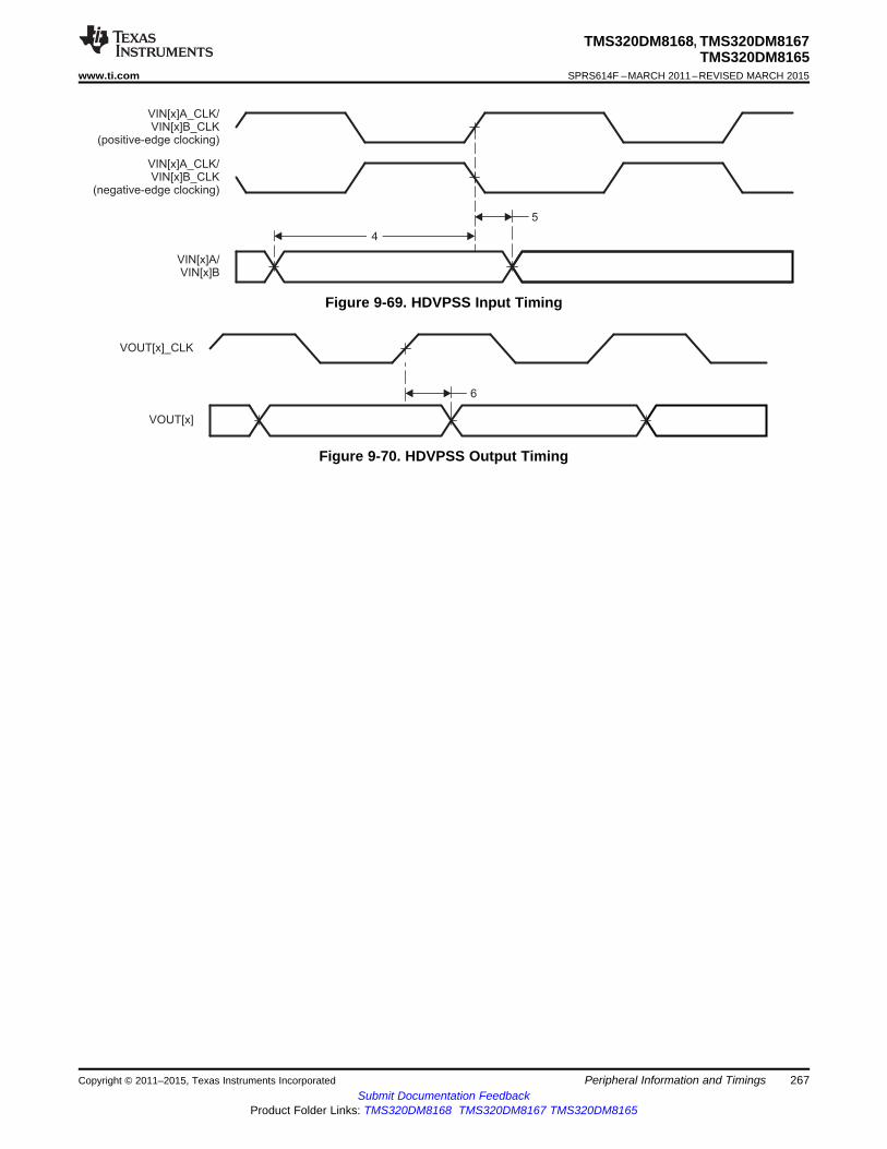
VOUT[x]_CLK
VOUT[x]
6
VIN[x]A_CLK/VIN[x]B_CLK
(positive-edge clocking)
4
VIN[x]A/VIN[x]B
5
VIN[x]A_CLK/VIN[x]B_CLK
(negative-edge clocking)
TMS320DM8168, TMS320DM8167TMS320DM8165
www.ti.com SPRS614F –MARCH 2011–REVISED MARCH 2015
Figure 9-69. HDVPSS Input Timing
Figure 9-70. HDVPSS Output Timing
Copyright © 2011–2015, Texas Instruments Incorporated Peripheral Information and Timings 267Submit Documentation Feedback
Product Folder Links: TMS320DM8168 TMS320DM8167 TMS320DM8165

RLOAD
ReconstructionFilter
IOUTx75 W
SD: 9.5 MHZED: 18 MHZHD: 36 MHz1080p: 72 MHz
Amplifier
SD: 5.6 V/VHD: 4.5 V/V
TMS320DM8168, TMS320DM8167TMS320DM8165SPRS614F –MARCH 2011–REVISED MARCH 2015 www.ti.com
9.10.2 Video DAC Guidelines and Electrical Data and TimingThe device's analog video DAC outputs are designed to drive a 37.5-Ω load. Figure 9-71 describes atypical circuit that permits connecting the analog video output from the device to standard 75-Ω impedancevideo systems. The device requires the use of a buffer to drive the actual video outputs, so one solution isto use a video amplifier with integrated buffer and internal filter, such as the Texas Instruments THS7360,which provides a complete solution for the typical output circuit shown in Figure 9-71.
Figure 9-71. Typical Output Circuits for Analog Video from DACs
During board design, the onboard traces and parasitics must be matched for the channel. The video DACoutput pin (IOUTx) is a very high-frequency analog signal and must be routed with extreme care. As aresult, the path of this signal must be as short as possible, and as isolated as possible from otherinterfering signals. The load resistor and amplifier or buffer should be placed close together and as closeas possible to the device pins. Other layout guidelines include:• Take special care to bypass the DAC power supply pin with a capacitor.• Place the 75-Ω resistor as close as possible (<0.5") to the amplifier or buffer (THS7360) output pin.• To maintain a high quality video signal, 75-Ω (±10%) characteristic impedance traces should be used
after the 75-Ω series resistor.• Minimize input trace lengths to the device to reduce parasitic capacitance.• Include solid ground return paths.• Match trace lengths as close as possible within a video format group (that is, Y, Pb, and Pr for
component output, and Y and C for s-video output should match each other).
For additional video DAC design guidelines, see the HDVPSS chapter in the TMS320DM816x DaVinciDigital Media Processors Technical Reference Manual (literature number SPRUGX8).
Table 9-73. DAC Specifications
PARAMETER CONDITIONS MIN TYP MAX UNITResolution HD DACs 12 Bits
SD DACs 10 BitsDC Accuracy - HD DACs
Integral Non-Linearity (INL), best fit HD DACs 1.5 LSBSD DACs 1.0 LSB
Differential Non-Linearity (DNL) HD DACs 1.0 LSBSD DACs 0.5 LSB
Analog OutputOutput Resistor (RLOAD) HD and SD DACs -1% 37.5 +1% ΩFull-Scale Output Current (IFS) HD and SD DACs 13.3 mA
RLOAD
Output Compliance Range HD and SD DACs 0 Vref VIFS = 13.3 mA,RLOAD = 37.5 Ω
Zero Scale Offset Error (ZSET) HD and SD DACs 0.5 LSBGain Error HD and SD DACs -10 10 %
268 Peripheral Information and Timings Copyright © 2011–2015, Texas Instruments IncorporatedSubmit Documentation Feedback
Product Folder Links: TMS320DM8168 TMS320DM8167 TMS320DM8165

TMS320DM8168, TMS320DM8167TMS320DM8165
www.ti.com SPRS614F –MARCH 2011–REVISED MARCH 2015
Table 9-73. DAC Specifications (continued)PARAMETER CONDITIONS MIN TYP MAX UNIT
Channel matching HD and SD DACs 2 %Recommended External Amplification HD DACs 4.5 V/V
SD DACs 5.6 V/VReference
Reference Voltage Range (VREF) Input with External -5% 0.5 +5% VReference
Full-Scale Current Adjust Resistors RBIAS_HD and RBIAS_SD -1% 1.2 +1% kΩDynamic Specifications
Output Update Rate (FCLK) HD DACs at 1080i60 74.25 MHzHD DACs at 1080p60 148.5 MHzSD DACs 27 54 MHz
Signal Bandwidth HD DACs at 1080i60 30 MHzHD DACs at 1080p60 60 MHzSD DACs 6 MHz
Spurious - Free Dynamic Range (SFDR) HD DACs at 1080i60 60 dBFCLK = 74.25 MHz,FOUT = 30 MHzHD DACs at 1080p60 60 dBFCLK = 148.5 MHz,FOUT = 60 MHzSD DACs 60 dBFCLK = 27 MHz / 54 MHz,FOUT = 6 MHz
Copyright © 2011–2015, Texas Instruments Incorporated Peripheral Information and Timings 269Submit Documentation Feedback
Product Folder Links: TMS320DM8168 TMS320DM8167 TMS320DM8165

TMS320DM8168, TMS320DM8167TMS320DM8165SPRS614F –MARCH 2011–REVISED MARCH 2015 www.ti.com
9.11 Inter-Integrated Circuit (I2C)The device includes two inter-integrated circuit (I2C) modules which provide an interface to other devicescompliant with Philips Semiconductors Inter-IC bus (I2C-bus™) specification version 2.1. Externalcomponents attached to this 2-wire serial bus can transmit or receive 8-bit data to or from the devicethrough the I2C module. The I2C port does not support CBUS compatible devices.
The I2C port supports the following features:• Compatible with Philips I2C Specification Revision 2.1 (January 2000)• Standard and fast modes from 10 - 400 Kbps (no fail-safe IO buffers)• Noise filter to remove noise 50 ns or less• Seven- and ten-bit device addressing modes• Multimaster transmitter or slave receiver mode• Multimaster receiver or slave transmitter mode• Combined master transmit/receive and receive or transmit modes• Two DMA channels, one interrupt line• Built-in FIFO (32 byte) for buffered read or write.
For more detailed information on the I2C peripheral, see the I2C chapter in the TMS320DM816x DaVinciDigital Media Processors Technical Reference Manual (literature number SPRUGX8).
9.11.1 I2C Peripheral Register Descriptions
Table 9-74. I2C Registers
I2C0 HEX ADDRESS I2C1 HEX ADDRESS ACRONYM REGISTER NAME0x4802 8000 0x4802 A000 I2C_REVNB_LO Module Revision (LOW BYTES)0x4802 8004 0x4802 A004 I2C_REVNB_HI Module Revision (HIGH BYTES)0x4802 8010 0x4802 A010 I2C_SYSC System configuration0x4802 8020 0x4802 A020 I2C_EOI I2C End of Interrupt0x4802 8024 0x4802 A024 I2C_IRQSTATUS_RAW I2C Status Raw0x4802 8028 0x4802 A028 I2C_IRQSTATUS I2C Status0x4802 802C 0x4802 A02C I2C_IRQENABLE_SET I2C Interrupt Enable Set0x4802 8030 0x4802 A030 I2C_IRQENABLE_CLR I2C Interrupt Enable Clear0x4802 8034 0x4802 A034 I2C_WE I2C Wakeup Enable0x4802 8038 0x4802 A038 I2C_DMARXENABLE_SET Receive DMA Enable Set0x4802 803C 0x4802 A03C I2C_DMATXENABLE_SET Transmit DMA Enable Set0x4802 8040 0x4802 A040 I2C_DMARXENABLE_CLR Receive DMA Enable Clear0x4802 8044 0x4802 A044 I2C_DMATXENABLE_CLR Transmit DMA Enable Clear0x4802 8048 0x4802 A048 I2C_DMARXWAKE_EN Receive DMA Wakeup0x4802 804C 0x4802 A04C I2C_DMATXWAKE_EN Transmit DMA Wakeup0x4802 8090 0x4802 A090 I2C_SYSS System Status0x4802 8094 0x4802 A094 I2C_BUF Buffer Configuration0x4802 8098 0x4802 A098 I2C_CNT Data Counter0x4802 809C 0x4802 A09C I2C_DATA Data Access0x4802 80A4 0x4802 A0A4 I2C_CON I2C Configuration0x4802 80A8 0x4802 A0A8 I2C_OA I2C Own Address0x4802 80AC 0x4802 A0AC I2C_SA I2C Slave Address0x4802 80B0 0x4802 A0B0 I2C_PSC I2C Clock Prescaler0x4802 80B4 0x4802 A0B4 I2C_SCLL I2C SCL Low Time0x4802 80B8 0x4802 A0B8 I2C_SCLH I2C SCL High Time0x4802 80BC 0x4802 A0BC I2C_SYSTEST System Test
270 Peripheral Information and Timings Copyright © 2011–2015, Texas Instruments IncorporatedSubmit Documentation Feedback
Product Folder Links: TMS320DM8168 TMS320DM8167 TMS320DM8165

TMS320DM8168, TMS320DM8167TMS320DM8165
www.ti.com SPRS614F –MARCH 2011–REVISED MARCH 2015
Table 9-74. I2C Registers (continued)I2C0 HEX ADDRESS I2C1 HEX ADDRESS ACRONYM REGISTER NAME
0x4802 80C0 0x4802 A0C0 I2C_BUFSTAT I2C Buffer Status0x4802 80C4 0x4802 A0C4 I2C_OA1 I2C Own Address 10x4802 80C8 0x4802 A0C8 I2C_OA2 I2C Own Address 20x4802 80CC 0x4802 A0CC I2C_OA3 I2C Own Address 30x4802 80D0 0x4802 A0D0 I2C_ACTOA Active Own Address0x4802 80D4 0x4802 A0D4 I2C_SBLOCK I2C Clock Blocking Enable
Copyright © 2011–2015, Texas Instruments Incorporated Peripheral Information and Timings 271Submit Documentation Feedback
Product Folder Links: TMS320DM8168 TMS320DM8167 TMS320DM8165

10
8
4
3
7
12
5
6 14
2
3
13
Stop Start RepeatedStart
Stop
I2C[x]_SDA
I2C[x]_SCL
1
11 9
TMS320DM8168, TMS320DM8167TMS320DM8165SPRS614F –MARCH 2011–REVISED MARCH 2015 www.ti.com
9.11.2 I2C Electrical Data and Timing
Table 9-75. Timing Requirements for I2C Input(see Figure 9-72)
NO. MIN MAX UNITStandard_IC 10
1 tc(SCL) Cycle time, SCL µsFast_IC 2.5Standard_IC 4.7Setup time, SCL high before SDA low (for a2 tsu(SCLH-SDAL) µsrepeated Start condition) Fast_IC 0.6Standard_IC 4Hold time, SCL low after SDA low (for a Start3 th(SDAL-SCLL) µsand a repeated Start condition) Fast_IC 0.6Standard_IC 4.7
4 tw(SCLL) Pulse duration, SCL low µsFast_IC 1.3Standard_IC 4
5 tw(SCLH) Pulse duration, SCL high µsFast_IC 0.6Standard_IC 250
6 tsu(SDAV-SCLH) Setup time, SDA valid before SCL high nsFast_IC 100Standard_IC 0 3.45Hold time, SDA valid after SCL low (for I2C7 th(SCLL-SDA) µsbus devices) Fast_IC 0 0.9Standard_IC 4.7Pulse duration, SDA high between Stop and8 tw(SDAH) µsStart conditions Fast_IC 1.3Standard_IC 4Setup time, high before SDA high (for Stop13 tsu(SCLH-SDAH) µscondition) Fast_IC 0.6
tw(SDA) Fast_IC 0 5014 Pulse duration, spike (must be suppressed) ns
tw(SCL) Fast_IC 0 50
Figure 9-72. I2C Receive Timing
272 Peripheral Information and Timings Copyright © 2011–2015, Texas Instruments IncorporatedSubmit Documentation Feedback
Product Folder Links: TMS320DM8168 TMS320DM8167 TMS320DM8165
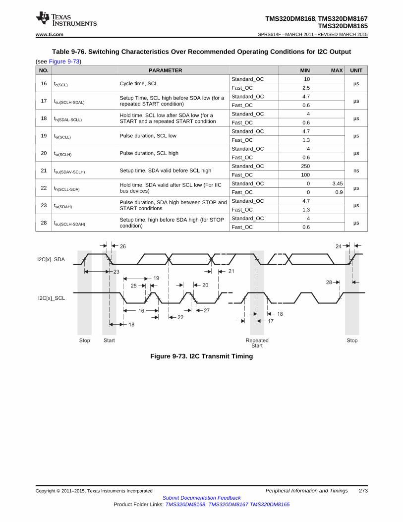
25
23
19
18
22
27
20
21
17
18
28
Stop Start RepeatedStart
Stop
I2C[x]_SDA
I2C[x]_SCL
16
26 24
TMS320DM8168, TMS320DM8167TMS320DM8165
www.ti.com SPRS614F –MARCH 2011–REVISED MARCH 2015
Table 9-76. Switching Characteristics Over Recommended Operating Conditions for I2C Output(see Figure 9-73)
NO. PARAMETER MIN MAX UNITStandard_OC 10
16 tc(SCL) Cycle time, SCL µsFast_OC 2.5Standard_OC 4.7Setup Time, SCL high before SDA low (for a17 tsu(SCLH-SDAL) µsrepeated START condition) Fast_OC 0.6Standard_OC 4Hold time, SCL low after SDA low (for a18 th(SDAL-SCLL) µsSTART and a repeated START condition Fast_OC 0.6Standard_OC 4.7
19 tw(SCLL) Pulse duration, SCL low µsFast_OC 1.3Standard_OC 4
20 tw(SCLH) Pulse duration, SCL high µsFast_OC 0.6Standard_OC 250
21 tsu(SDAV-SCLH) Setup time, SDA valid before SCL high nsFast_OC 100Standard_OC 0 3.45Hold time, SDA valid after SCL low (For IIC22 th(SCLL-SDA) µsbus devices) Fast_OC 0 0.9Standard_OC 4.7Pulse duration, SDA high between STOP and23 tw(SDAH) µsSTART conditions Fast_OC 1.3Standard_OC 4Setup time, high before SDA high (for STOP28 tsu(SCLH-SDAH) µscondition) Fast_OC 0.6
Figure 9-73. I2C Transmit Timing
Copyright © 2011–2015, Texas Instruments Incorporated Peripheral Information and Timings 273Submit Documentation Feedback
Product Folder Links: TMS320DM8168 TMS320DM8167 TMS320DM8165

TMS320DM8168, TMS320DM8167TMS320DM8165SPRS614F –MARCH 2011–REVISED MARCH 2015 www.ti.com
9.12 Multichannel Audio Serial Port (McASP)The multichannel audio serial port (McASP) functions as a general-purpose audio serial port optimized forthe needs of multichannel audio applications. The McASP is useful for time-division multiplexed (TDM)stream, Inter-Integrated Sound (I2S) protocols, and intercomponent digital audio interface transmission(DIT).
9.12.1 McASP Device-Specific InformationThe device includes three multichannel audio serial port (McASP) interface peripherals (McASP0,McASP1, and McASP2). The McASP module consists of a transmit and receive section. These sectionscan operate completely independently with different data formats, separate master clocks, bit clocks, andframe syncs or, alternatively, the transmit and receive sections may be synchronized. The McASP modulealso includes shift registers that may be configured to operate as either transmit data or receive data. Thetransmit section of the McASP can transmit data in either a time-division-multiplexed (TDM) synchronousserial format or in a digital audio interface (DIT) format where the bit stream is encoded for SPDIF, AES-3,IEC-60958, CP-430 transmission. The receive section of the McASP peripheral supports the TDMsynchronous serial format.
The McASP module can support one transmit data format (either a TDM format or DIT format) and onereceive format at a time. All transmit shift registers use the same format and all receive shift registers usethe same format; however, the transmit and receive formats need not be the same. Both the transmit andreceive sections of the McASP also support burst mode, which is useful for non-audio data (for example,passing control information between two devices).
The McASP peripheral has additional capability for flexible clock generation and error detection andhandling, as well as error management.
The device McASP0 module has six serial data pins, while McASP1 and McASP2 are limited to two serialdata pins each.
The McASP FIFO size is 256 bytes and two DMA and two interrupt requests are supported. Buffers areused transparently to better manage DMA, which can be leveraged to manage data flow more efficiently.
For more detailed information on and the functionality of the McASP peripheral, see the McASP chapter inthe TMS320DM816x DaVinci Digital Media Processors Technical Reference Manual (literature numberSPRUGX8).
274 Peripheral Information and Timings Copyright © 2011–2015, Texas Instruments IncorporatedSubmit Documentation Feedback
Product Folder Links: TMS320DM8168 TMS320DM8167 TMS320DM8165

TMS320DM8168, TMS320DM8167TMS320DM8165
www.ti.com SPRS614F –MARCH 2011–REVISED MARCH 2015
9.12.2 McASP0, McASP1, and McASP2 Peripheral Register Descriptions
Table 9-77. McASP0, McASP1, and McASP2 Registers
MCASP0 ADDRESS MCASP1 ADDRESS MCASP2 ADDRESS ACRONYM REGISTER NAME0x4803 8000 0x4803 C000 0x4805 0000 PID Peripheral ID0x4803 8004 0x4803 C004 0x4805 0004 PWRIDLE Power Idle SYSCONFIG
SYSCONFIG0x4803 8010 0x4803 C010 0x4805 0010 PFUNC Pin Function0x4803 8014 0x4803 C014 0x4805 0014 PDIR Pin Direction0x4803 8018 0x4803 C018 0x4805 0018 PDOUT Pin Data Out
PDIN Pin Data Input (Read)Read returns pin data input
PDSET Pin Data Set (Write)0x4803 801C 0x4803 C01C 0x4805 001CWrites effect pin data set(alternate write addressPDOUT)
0x4803 8020 0x4803 C020 0x4805 0020 PDCLR Pin Data Clear0x4803 8044 0x4803 C044 0x4805 0044 GBLCTL Global Control0x4803 8048 0x4803 C048 0x4805 0048 AMUTE Mute Control0x4803 804C 0x4803 C04C 0x4805 004C LBCTL Loop-Back Test Control0x4803 8050 0x4803 C050 0x4805 0050 TXDITCTL Transmit DIT Mode Control0x4803 8060 0x4803 C060 0x4805 0060 GBLCTLR Alias of GBLCTL containing
only receiver reset bits;allows transmit to be resetindependently from receive
0x4803 8064 0x4803 C064 0x4805 0064 RXMASK Receiver Bit Mask0x4803 8068 0x4803 C068 0x4805 0068 RXFMT Receive Bitstream Format0x4803 806C 0x4803 C06C 0x4805 006C RXFMCTL Receive Frame Sync
Control0x4803 8070 0x4803 C070 0x4805 0070 ACLKRCTL Receive Clock Control0x4803 8074 0x4803 C074 0x4805 0074 AHCLKRCTL High Frequency Receive
Clock Control0x4803 8078 0x4803 C078 0x4805 0078 RXTDM Receive TDM Slot 0-310x4803 807C 0x4803 C07C 0x4805 007C EVTCTLR Receiver Interrupt Control0x4803 8080 0x4803 C080 0x4805 0080 RXSTAT Status Receiver0x4803 8084 0x4803 C084 0x4805 0084 RXTDMSLOT Current Receive TDM Slot0x4803 8088 0x4803 C088 0x4805 0088 RXCLKCHK Receiver Clock Check
Control0x4803 808C 0x4803 C08C 0x4805 008C REVTCTL Receiver DMA Event
Control0x4803 80A0 0x4803 C0A0 0x4805 00A0 GBLCTLX Alias of GBLCTL containing
only transmit reset bits;allows transmit to be resetindependently from receive
0x4803 80A4 0x4803 C0A4 0x4805 00A4 TXMASK Transmit Format Unit BitMask
0x4803 80A8 0x4803 C0A8 0x4805 00A8 TXFMT Transmit Bitstream Format0x4803 80AC 0x4803 C0AC 0x4805 00AC TXFMCTL Transmit Frame Sync
Control0x4803 80B0 0x4803 C0B0 0x4805 00B0 ACLKXCTL Transmit Clock Control0x4803 80B4 0x4803 C0B4 0x4805 00B4 AHCLKXCTL High Frequency Transmit
Clock Control0x4803 80B8 0x4803 C0B8 0x4805 00B8 TXTDM Transmit TDM Slot 0-310x4803 80BC 0x4803 C0BC 0x4805 00BC EVTCTLX Transmitter Interrupt Control0x4803 80C0 0x4803 C0C0 0x4805 00C0 TXSTAT Status Transmitter
Copyright © 2011–2015, Texas Instruments Incorporated Peripheral Information and Timings 275Submit Documentation Feedback
Product Folder Links: TMS320DM8168 TMS320DM8167 TMS320DM8165

TMS320DM8168, TMS320DM8167TMS320DM8165SPRS614F –MARCH 2011–REVISED MARCH 2015 www.ti.com
Table 9-77. McASP0, McASP1, and McASP2 Registers (continued)MCASP0 ADDRESS MCASP1 ADDRESS MCASP2 ADDRESS ACRONYM REGISTER NAME
0x4803 80C4 0x4803 C0C4 0x4805 00C4 TXTDMSLOT Current Transmit TDM Slot0x4803 80C8 0x4803 C0C8 0x4805 00C8 TXCLKCHK Transmit Clock Check
Control0x4803 80CC 0x4803 C0CC 0x4805 00CC XEVTCTL Transmitter DMA Control0x4803 80D0 0x4803 C0D0 0x4805 00D0 CLKADJEN One-shot Clock Adjust
Enable0x4803 8100 0x4803 C100 0x4805 0100 DITCSRA0 Left (Even TDM Slot)
Channel Status RegisterFile
0x4803 8104 0x4803 C104 0x4805 0104 DITCSRA1 Left (Even TDM Slot)Channel Status RegisterFile
0x4803 8108 0x4803 C108 0x4805 0108 DITCSRA2 Left (Even TDM Slot)Channel Status RegisterFile
0x4803 810C 0x4803 C10C 0x4805 010C DITCSRA3 Left (Even TDM Slot)Channel Status RegisterFile
0x4803 8110 0x4803 C110 0x4805 0110 DITCSRA4 Left (Even TDM Slot)Channel Status RegisterFile
0x4803 8114 0x4803 C114 0x4805 0114 DITCSRA5 Left (Even TDM Slot)Channel Status RegisterFile
0x4803 8118 0x4803 C118 0x4805 0118 DITCSRB0 Right (Odd TDM Slot)Channel Status RegisterFile
0x4803 811C 0x4803 C11C 0x4805 011C DITCSRB1 Right (Odd TDM Slot)Channel Status RegisterFile
0x4803 8120 0x4803 C120 0x4805 0120 DITCSRB2 Right (Odd TDM Slot)Channel Status RegisterFile
0x4803 8124 0x4803 C124 0x4805 0124 DITCSRB3 Right (Odd TDM Slot)Channel Status RegisterFile
0x4803 8128 0x4803 C128 0x4805 0128 DITCSRB4 Right (Odd TDM Slot)Channel Status RegisterFile
0x4803 812C 0x4803 C12C 0x4805 012C DITCSRB5 Right (Odd TDM Slot)Channel Status RegisterFile
0x4803 8130 0x4803 C130 0x4805 0130 DITUDRA0 Left (Even TDM Slot) UserData Register File
0x4803 8134 0x4803 C134 0x4805 0134 DITUDRA1 Left (Even TDM Slot) UserData Register File
0x4803 8138 0x4803 C138 0x4805 0138 DITUDRA2 Left (Even TDM Slot) UserData Register File
0x4803 813C 0x4803 C13C 0x4805 013C DITUDRA3 Left (Even TDM Slot) UserData Register File
0x4803 8140 0x4803 C140 0x4805 0140 DITUDRA4 Left (Even TDM Slot) UserData Register File
0x4803 8144 0x4803 C144 0x4805 0144 DITUDRA5 Left (Even TDM Slot) UserData Register File
0x4803 8148 0x4803 C148 0x4805 0148 DITUDRB0 Right (Odd TDM Slot) UserData Register File
0x4803 814C 0x4803 C14C 0x4805 014C DITUDRB1 Right (Odd TDM Slot) UserData Register File
276 Peripheral Information and Timings Copyright © 2011–2015, Texas Instruments IncorporatedSubmit Documentation Feedback
Product Folder Links: TMS320DM8168 TMS320DM8167 TMS320DM8165
TMS320DM8168, TMS320DM8167TMS320DM8165
www.ti.com SPRS614F –MARCH 2011–REVISED MARCH 2015
Table 9-77. McASP0, McASP1, and McASP2 Registers (continued)MCASP0 ADDRESS MCASP1 ADDRESS MCASP2 ADDRESS ACRONYM REGISTER NAME
0x4803 8150 0x4803 C150 0x4805 0150 DITUDRB2 Right (Odd TDM Slot) UserData Register File
0x4803 8154 0x4803 C154 0x4805 0154 DITUDRB3 Right (Odd TDM Slot) UserData Register File
0x4803 8158 0x4803 C158 0x4805 0158 DITUDRB4 Right (Odd TDM Slot) UserData Register File
0x4803 815C 0x4803 C15C 0x4805 015C DITUDRB5 Right (Odd TDM Slot) UserData Register File
0x4803 8180 - 0x4803 C180 - 0x4805 0180 - 0x4805 XRSRCTL0 - Serializer 0 Control -0x4803 81BC 0x4803 C1BC 01BC XRSRCTL15 Serializer 15 Control0x4803 8200 - 0x4803 C200 - 0x4805 0200 - 0x4805 023C TXBUF0 - Transmit Buffer for0x4803 8 23C 0x4803 C23C TXBUF15 Serializer 0 - Transmit
Buffer for Serializer 150x4803 8280 - 0x4803 C280 - 0x4805 0280 - 0x4805 RXBUF0 - Receive Buffer for Serializer0x4803 82BC 0x4803 C2BC 02BC RXBUF15 0 - Receive Buffer for
Serializer 150x4803 9000 0x4803 D000 0x4805 1000 BUFFER_CFGRD Write FIFO Control
_WFIFOCTL0x4803 9004 0x4803 D004 0x4805 1004 BUFFER_CFGRD Write FIFO Status
_WFIFOSTS0x4803 9008 0x4803 D008 0x4805 1008 BUFFER_CFGRD Read FIFO Control
_RFIFOCTL0x4803 900C 0x4803 D00C 0x4805 100C BUFFER_CFGRD Read FIFO Status
_RFIFOSTS
Table 9-78. McASP Registers Accessed Through DAT Port
HEX REGISTER McASP0 BYTE McASP0 BYTE McASP0 BYTE REGISTER DESCRIPTIONADDRESS NAME ADDRESS ADDRESS ADDRESSRead Accesses RBUF 4600 0000 4640 0000 4680 0000 Receive buffer DMA port address. Cycles through
receive serializers, skipping over transmitserializers and inactive serializers. Starts at thelowest serializer at the beginning of each timeslot. Reads from DMA port only if XBUSEL = 0 inXFMT.
Write Accesses XBUF 4600 0000 4640 0000 4680 0000 Transmit buffer DMA port address. Cycles throughtransmit serializers, skipping over receive andinactive serializers. Starts at the lowest serializerat the beginning of each time slot. Writes to DMAport only if RBUSEL = 0 in RFMT.
Copyright © 2011–2015, Texas Instruments Incorporated Peripheral Information and Timings 277Submit Documentation Feedback
Product Folder Links: TMS320DM8168 TMS320DM8167 TMS320DM8165
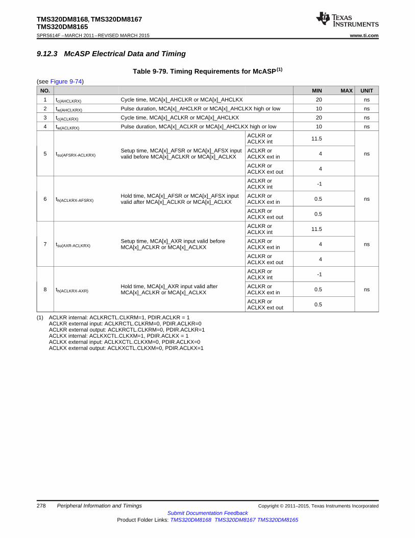
TMS320DM8168, TMS320DM8167TMS320DM8165SPRS614F –MARCH 2011–REVISED MARCH 2015 www.ti.com
9.12.3 McASP Electrical Data and Timing
Table 9-79. Timing Requirements for McASP (1)
(see Figure 9-74)NO. MIN MAX UNIT
1 tc(AHCLKRX) Cycle time, MCA[x]_AHCLKR or MCA[x]_AHCLKX 20 ns2 tw(AHCLKRX) Pulse duration, MCA[x]_AHCLKR or MCA[x]_AHCLKX high or low 10 ns3 tc(ACLKRX) Cycle time, MCA[x]_ACLKR or MCA[x]_AHCLKX 20 ns4 tw(ACLKRX) Pulse duration, MCA[x]_ACLKR or MCA[x]_AHCLKX high or low 10 ns
ACLKR or 11.5ACLKX intSetup time, MCA[x]_AFSR or MCA[x]_AFSX input ACLKR or5 tsu(AFSRX-ACLKRX) 4 nsvalid before MCA[x]_ACLKR or MCA[x]_ACLKX ACLKX ext in
ACLKR or 4ACLKX ext outACLKR or -1ACLKX int
Hold time, MCA[x]_AFSR or MCA[x]_AFSX input ACLKR or6 th(ACLKRX-AFSRX) 0.5 nsvalid after MCA[x]_ACLKR or MCA[x]_ACLKX ACLKX ext inACLKR or 0.5ACLKX ext outACLKR or 11.5ACLKX int
Setup time, MCA[x]_AXR input valid before ACLKR or7 tsu(AXR-ACLKRX) 4 nsMCA[x]_ACLKR or MCA[x]_ACLKX ACLKX ext inACLKR or 4ACLKX ext outACLKR or -1ACLKX int
Hold time, MCA[x]_AXR input valid after ACLKR or8 th(ACLKRX-AXR) 0.5 nsMCA[x]_ACLKR or MCA[x]_ACLKX ACLKX ext inACLKR or 0.5ACLKX ext out
(1) ACLKR internal: ACLKRCTL.CLKRM=1, PDIR.ACLKR = 1ACLKR external input: ACLKRCTL.CLKRM=0, PDIR.ACLKR=0ACLKR external output: ACLKRCTL.CLKRM=0, PDIR.ACLKR=1ACLKX internal: ACLKXCTL.CLKXM=1, PDIR.ACLKX = 1ACLKX external input: ACLKXCTL.CLKXM=0, PDIR.ACLKX=0ACLKX external output: ACLKXCTL.CLKXM=0, PDIR.ACLKX=1
278 Peripheral Information and Timings Copyright © 2011–2015, Texas Instruments IncorporatedSubmit Documentation Feedback
Product Folder Links: TMS320DM8168 TMS320DM8167 TMS320DM8165

8
7
4
43
2
21
A0 A1 B0 B1A30 A31 B30 B31 C0 C1 C2 C3 C31
MCA[x]_ACLKR/X (Falling Edge Polarity)
MCA[x]_AHCLKR/X (Rising Edge Polarity)
MCA[x]_AFSR/X (Bit Width, 0 Bit Delay)
MCA[x]_AFSR/X (Bit Width, 1 Bit Delay)
MCA[x]_AFSR/X (Bit Width, 2 Bit Delay)
MCA[x]_AFSR/X (Slot Width, 0 Bit Delay)
MCA[x]_AFSR/X (Slot Width, 1 Bit Delay)
MCA[x]_AFSR/X (Slot Width, 2 Bit Delay)
MCA[x]_AXR[x] (Data In/Receive)
6
5
MCA[x]_ACLKR/X (CLKRP = CLKXP = 0)(A)
MCA[x]_ACLKR/X (CLKRP = CLKXP = 1)(B)
TMS320DM8168, TMS320DM8167TMS320DM8165
www.ti.com SPRS614F –MARCH 2011–REVISED MARCH 2015
A. For CLKRP = CLKXP = 0, the McASP transmitter is configured for rising edge (to shift data out) and the McASPreceiver is configured for falling edge (to shift data in).
B. For CLKRP = CLKXP = 1, the McASP transmitter is configured for falling edge (to shift data out) and the McASPreceiver is configured for rising edge (to shift data in).
Figure 9-74. McASP Input Timing
Copyright © 2011–2015, Texas Instruments Incorporated Peripheral Information and Timings 279Submit Documentation Feedback
Product Folder Links: TMS320DM8168 TMS320DM8167 TMS320DM8165

TMS320DM8168, TMS320DM8167TMS320DM8165SPRS614F –MARCH 2011–REVISED MARCH 2015 www.ti.com
Table 9-80. Switching Characteristics Over Recommended Operating Conditions for McASP (1)
(see Figure 9-75)NO. PARAMETER MIN MAX UNIT
9 tc(AHCLKRX) Cycle time, MCA[x]_AHCLKR/X 20 (2) ns0.5P -10 tw(AHCLKRX) Pulse duration, MCA[x]_AHCLKR/X high or low ns2.5 (3)
11 tc(ACLKRX) Cycle time, MCA[x]_ACLKR or ACLKX 20 ns0.5P -12 tw(ACLKRX) Pulse duration, MCA[x]_ACLKR or ACLKX high or low ns2.5 (3)
ACLKR or 0 6ACLKX intDelay time, MCA[x]_ACLKR or ACLKX transmitedge to MCA[x]_AFSR/X output valid ACLKR or 2 13.513 td(ACLKRX-AFSRX) ACLKX ext in nsDelay time, MCA[x]_ACLKR or ACLKX transmit ACLKR oredge to MCA[x]_AFSR/X output valid with Pad 2 13.5ACLKX ext outLoopback
ACLKX int -1 5Delay time, MCA[x]_ACLKX transmit edge toMCA[x]_AXR output valid ACLKX ext in 2 13.514 td(ACLKX-AXR) nsDelay time, MCA[x]_ACLKX transmit edge to ACLKX ext out 2 13.5MCA[x]_AXR output valid with Pad Loopback
ACLKX int -1 5Disable time, MCA[x]_ACLKX transmit edge toMCA[x]_AXR output high impedance ACLKX ext in 2 13.5
15 tdis(ACLKX-AXR) nsDisable time, MCA[x]_ACLKX transmit edge toMCA[x]_AXR output high impedance with Pad ACLKX ext out 2 13.5Loopback
(1) ACLKR internal: ACLKRCTL.CLKRM=1, PDIR.ACLKR = 1ACLKR external input: ACLKRCTL.CLKRM=0, PDIR.ACLKR=0ACLKR external output: ACLKRCTL.CLKRM=0, PDIR.ACLKR=1ACLKX internal: ACLKXCTL.CLKXM=1, PDIR.ACLKX = 1ACLKX external input: ACLKXCTL.CLKXM=0, PDIR.ACLKX=0ACLKX external output: ACLKXCTL.CLKXM=0, PDIR.ACLKX=1
(2) 50 MHz(3) P = AHCLKR or AHCLKX period.
280 Peripheral Information and Timings Copyright © 2011–2015, Texas Instruments IncorporatedSubmit Documentation Feedback
Product Folder Links: TMS320DM8168 TMS320DM8167 TMS320DM8165

15
14
1313
12
1211
10
10
9
A0 A1 B0 B1A30 A31 B30 B31 C0 C1 C2 C3 C31
1313
13 1313
MCA[x]_ACLKR/X (Falling Edge Polarity)
MCA[x]_AHCLKR/X (Rising Edge Polarity)
MCA[x]_AFSR/X (Bit Width, 0 Bit Delay)
MCA[x]_AFSR/X (Bit Width, 1 Bit Delay)
MCA[x]_AFSR/X (Bit Width, 2 Bit Delay)
MCA[x]_AFSR/X (Slot Width, 0 Bit Delay)
MCA[x]_AFSR/X (Slot Width, 1 Bit Delay)
MCA[x]_AFSR/X (Slot Width, 2 Bit Delay)
MCA[x]_AXR[x] (Data Out/Transmit)
MCA[x]_ACLKR/X (CLKRP = CLKXP = 1)(A)
MCA[x]_ACLKR/X (CLKRP = CLKXP = 0)(B)
TMS320DM8168, TMS320DM8167TMS320DM8165
www.ti.com SPRS614F –MARCH 2011–REVISED MARCH 2015
A. For CLKRP = CLKXP = 1, the McASP transmitter is configured for falling edge (to shift data out) and the McASPreceiver is configured for rising edge (to shift data in).
B. For CLKRP = CLKXP = 0, the McASP transmitter is configured for rising edge (to shift data out) and the McASPreceiver is configured for falling edge (to shift data in).
Figure 9-75. McASP Output Timing
Copyright © 2011–2015, Texas Instruments Incorporated Peripheral Information and Timings 281Submit Documentation Feedback
Product Folder Links: TMS320DM8168 TMS320DM8167 TMS320DM8165

TMS320DM8168, TMS320DM8167TMS320DM8165SPRS614F –MARCH 2011–REVISED MARCH 2015 www.ti.com
9.13 Multichannel Buffered Serial Port (McBSP)The McBSP provides these functions:• Full-duplex communication• Double-buffered data registers, which allow a continuous data stream• Independent framing and clocking for receive and transmit• Direct interface to industry-standard codecs, analog interface chips (AICs), and other serially
connected analog-to-digital (AD) and digital-to-analog (DA) devices• Supports TDM, I2S, and similar formats• External shift clock or an internal, programmable frequency shift clock for data transfer• 5KB Tx and Rx buffer• Supports three interrupt and two DMA requests.
The McBSP module may support two types of data transfer at the system level:• The full-cycle mode, for which one clock period is used to transfer the data, generated on one edge
and captured on the same edge (one clock period later).• The half-cycle mode, for which one half clock period is used to transfer the data, generated on one
edge and captured on the opposite edge (one half clock period later). Note that a new data isgenerated only every clock period, which secures the required hold time. The interface clock (CLKX orCLKR) activation edge (data or frame sync capture and generation) has to be configured accordinglywith the external peripheral (activation edge capability) and the type of data transfer required at thesystem level.
For more detailed information on the McBSP peripheral, see the McBSP chapter in the TMS320DM816xDaVinci Digital Media Processors Technical Reference Manual (literature number SPRUGX8).
The following sections describe the timing characteristics for applications in normal mode (that is, theMcBSP connected to one peripheral) and TDM applications in multipoint mode.
9.13.1 McBSP Peripheral RegistersThis McBSP peripheral registers are described in the TMS320DM816x DaVinci Digital Media ProcessorsTechnical Reference Manual (literature number SPRUGX8). Each register is documented as an offsetfrom a base address for the peripheral. The base addresses for all of the peripherals are shown inTable 3-26, L3 Memory Map.
282 Peripheral Information and Timings Copyright © 2011–2015, Texas Instruments IncorporatedSubmit Documentation Feedback
Product Folder Links: TMS320DM8168 TMS320DM8167 TMS320DM8165

MCB_CLK
MCB_FS
MCB_DX
MCB_DR
MCB_DX7
4
5
1 23
6
7
MCB_DX6 MCB_DX0
MCB_DR7 MCB_DR6 MCB_DR0
4
5 5
TMS320DM8168, TMS320DM8167TMS320DM8165
www.ti.com SPRS614F –MARCH 2011–REVISED MARCH 2015
9.13.2 McBSP Electrical Data and Timing
Table 9-81. Timing Requirements for McBSP - Master Mode (1)
(see Figure 9-76)NO. MIN MAX UNIT
6 tsu(DRV-CLKAE) Setup time, MCB_DR valid before MCB_CLK active edge (2) 3.5 ns7 th(CLKAE-DRV) Hold time, MCB_DR valid after MCB_CLK active edge (2) 0.1 ns
(1) The timings apply to all configurations regardless of MCB_CLK polarity and which clock edges are used to drive output data and captureinput data.
(2) MCB_CLK corresponds to either MCB_CLKX or MCB_CLKR.
Table 9-82. Switching Characteristics Over Recommended Operating Conditions for McBSP - MasterMode (1)
(see Figure 9-76)NO. PARAMETER MIN MAX UNIT
1 tc(CLK) Cycle time, output MCB_CLK period (2) 20.83 ns2 tw(CLKL) Pulse duration, output MCB_CLK low (2) 0.5*P - 1 (3) ns3 tw(CLKH) Pulse duration, output MCB_CLK high (2) 0.5*P - 1 (3) ns
Delay time, output MCB_CLK active edge to output MCB_FS4 td(CLKAE-FSV) 0.7 9.4 nsvalid (2) (4)
Delay time, output MCB_CLKX active edge to output MCB_DX5 td(CLKXAE-DXV) 0.7 9.4 nsvalid
(1) The timings apply to all configurations regardless of MCB_CLK polarity and which clock edges are used to drive output data and captureinput data.
(2) MCB_CLK corresponds to either MCB_CLKX or MCB_CLKR.(3) P = MCB_CLKX or MCB_CLKR output CLK period, in ns; use whichever value is greater. This parameter applies to the maximum
McBSP frequency. Operate serial clocks (CLKX or CLKR) in the reasonable range of 40-60 duty cycle.(4) MCB_FS corresponds to either MCB_FSX or MCB_FSR.
A. The timings apply to all configurations regardless of MCB_CLK polarity and which clock edges are used to driveoutput data and capture input data.
B. MCBSP_CLK corresponds to either MCBSP_CLKX or MCBSP_CLKR; MCBSP_FS corresponds to eitherMCBSP_FSX or MCBSP_FSR.McBSP in 6-pin mode: DX and DR as data pins; CLKX, CLKR, FSX and FSR as control pins.McBSP in 4-pin mode: DX and DR as data pins; CLKX and FSX pins as control pins. The CLKX and FSX pins areinternally looped back via software configuration, respectively to the CLKR and FSR internal signals for data receive.
C. The polarity of McBSP frame synchronization is software configurable.D. The active clock edge selection of MCBSP_CLK (rising or falling) on which MCBSP_DX data is latched and
MCBSP_DR data is sampled is software configurable.E. Timing diagrams are for data delay set to 1.F. For further details about the registers used to configure McBSP, see the McBSP chapter in the TMS320DM816x
DaVinci Digital Media Processors Technical Reference Manual (literature number SPRUGX8).
Figure 9-76. McBSP Master Mode Timing
Copyright © 2011–2015, Texas Instruments Incorporated Peripheral Information and Timings 283Submit Documentation Feedback
Product Folder Links: TMS320DM8168 TMS320DM8167 TMS320DM8165

MCB_CLK
MCB_FS
MCB_DX
MCB_DR
MCB_DX7
6
1 23
7
8
MCB_DX6 MCB_DX0
MCB_DR7 MCB_DR6 MCB_DR0
4
6 6
45
TMS320DM8168, TMS320DM8167TMS320DM8165SPRS614F –MARCH 2011–REVISED MARCH 2015 www.ti.com
Table 9-83. Timing Requirements for McBSP - Slave Mode (1)
(see Figure 9-77)NO. MIN MAX UNIT
1 tc(CLK) Cycle time, MCB_CLK period (2) 20.83 ns2 tw(CLKL) Pulse duration, MCB_CLK low (2) 0.5*P - 1 (3) ns3 tw(CLKH) Pulse duration, MCB_CLK high (2) 0.5*P - 1 (3) ns4 tsu(FSV-CLKAE) Setup time, MCB_FS valid before MCB_CLK active edge (2) (4) 3.8 ns5 th(CLKAE-FSV) Hold time, MCB_FS valid after MCB_CLK active edge (2) (4) 0 ns7 tsu(DRV-CLKAE) Setup time, MCB_DR valid before MCB_CLK active edge (2) 3.8 ns8 th(CLKAE-DRV) Hold time, MCB_DR valid after MCB_CLK active edge (2) 0 ns
(1) The timings apply to all configurations regardless of MCB_CLK polarity and which clock edges are used to drive output data and captureinput data.
(2) MCB_CLK corresponds to either MCB_CLKX or MCB_CLKR.(3) P = MCB_CLKX or MCB_CLKR output CLK period, in ns; use whichever value is greater. This parameter applies to the maximum
McBSP frequency. Operate serial clocks (CLKX or CLKR) in the reasonable range of 40-60 duty cycle.(4) MCB_FS corresponds to either MCB_FSX or MCB_FSR.
Table 9-84. Switching Characteristics Over Recommended Operating Conditions for McBSP - SlaveMode (1)
(see Figure 9-77)NO. PARAMETER MIN MAX UNIT
6 td(CLKXAE-DXV) Delay time, input MCB_CLKx active edge to output MCB_DX valid 0.5 12.5 ns
(1) The timings apply to all configurations regardless of MCB_CLK polarity and which clock edges are used to drive output data and captureinput data.
A. The timings apply to all configurations regardless of MCB_CLK polarity and which clock edges are used to driveoutput data and capture input data.
B. MCBSP_CLK corresponds to either MCBSP_CLKX or MCBSP_CLKR; MCBSP_FS corresponds to eitherMCBSP_FSX or MCBSP_FSR.McBSP in 6-pin mode: DX and DR as data pins; CLKX, CLKR, FSX and FSR as control pins.McBSP in 4-pin mode: DX and DR as data pins; CLKX and FSX pins as control pins. The CLKX and FSX pins areinternally looped back via software configuration, respectively to the CLKR and FSR internal signals for data receive.
C. The polarity of McBSP frame synchronization is software configurable.D. The active clock edge selection of MCBSP_CLK (rising or falling) on which MCBSP_DX data is latched and
MCBSP_DR data is sampled is software configurable.E. Timing diagrams are for data delay set to 1.F. For further details about the registers used to configure McBSP, see the McBSP chapter in the TMS320DM816x
DaVinci Digital Media Processors Technical Reference Manual (literature number SPRUGX8).
Figure 9-77. McBSP Slave Mode Timing
284 Peripheral Information and Timings Copyright © 2011–2015, Texas Instruments IncorporatedSubmit Documentation Feedback
Product Folder Links: TMS320DM8168 TMS320DM8167 TMS320DM8165
TMS320DM8168, TMS320DM8167TMS320DM8165
www.ti.com SPRS614F –MARCH 2011–REVISED MARCH 2015
9.14 Peripheral Component Interconnect Express (PCIe)The device supports connections to PCIe-compliant devices via the integrated PCIe master or slave businterface. The PCIe module is comprised of a dual-mode PCIe core and a SerDes PHY. The deviceimplements a single two-lane PCIe 2.0 (5.0 GT/s) endpoint or root complex port.
The device PCIe supports the following features:• Supports Gen1 and Gen2 in x1 or x2 mode• One port with up to 2 x 5 GT/s lanes• Single virtual channel (VC), single traffic class (TC)• Single function in end-point mode• Automatic width and speed negotiation and lane reversal• Max payload: 128 byte outbound, 256 byte inbound• Automatic credit management• ECRC generation and checking• Configurable BAR filtering• Supports PCIe messages• Legacy interrupt reception (RC) and generation (EP)• MSI generation and reception• PCI device power management, except D3 cold with vaux• Active state power management state L0 and L1.
For more detailed information on the PCIe port peripheral module, see the PCIe chapter in theTMS320DM816x DaVinci Digital Media Processors Technical Reference Manual (literature numberSPRUGX8).
The PCIe peripheral on the device conforms to the PCI Express Base 2.0 Specification.
9.14.1 PCIe Design and Layout Specifications
NOTEFor more information on PCB layout, see the DM816xx Easy CYG Package PCB EscapeRouting application report (literature number SPRABK6).
9.14.1.1 Clock Source
A standard 100-MHz PCIe differential clock source must be used for PCIe operation (for details, seeSection 8.3.2).
9.14.1.2 PCIe Connections and Interface Compliance
The PCIe interface on the device is compliant with the PCI Express Base 2.0 Specification. Refer to thePCIe specifications for all connections that are described in it. For coupling capacitor selection, seeSection 9.14.1.2.1.
The use of PCIe-compatible bridges and switches is allowed for interfacing with more than one otherprocessor or PCIe device.
9.14.1.2.1 Coupling Capacitors
AC coupling capacitors are required on the transmit data pair. Table 9-85 shows the requirements forthese capacitors.
Copyright © 2011–2015, Texas Instruments Incorporated Peripheral Information and Timings 285Submit Documentation Feedback
Product Folder Links: TMS320DM8168 TMS320DM8167 TMS320DM8165

TMS320DM8168, TMS320DM8167TMS320DM8165SPRS614F –MARCH 2011–REVISED MARCH 2015 www.ti.com
Table 9-85. AC Coupling Capacitors Requirements
PARAMETER MIN TYP MAX UNITPCIe AC coupling capacitor value 75 200 nFPCIe AC coupling capacitor package size (1) 0402 0603 EIA (2)
(1) The physical size of the capacitor should be as small as practical. Use the same size on both lines in each pair, placed side by side.(2) EIA LxW units; for example, a 0402 is a 40x20 mil (thousandths of an inch) surface-mount capacitor.
9.14.1.2.2 Polarity Inversion
The PCIe specification requires polarity inversion support. This means, for layout purposes, polarity isunimportant since each signal can change its polarity on-die inside the chip. This means polarity within alane is unimportant for layout.
9.14.1.2.3 Lane Reversal
The device supports lane reversal. Since there are two lanes, this means the lanes can be switched inlayout for better PCB routing.
9.14.1.3 Non-Standard PCIe Connections
The following sections contain suggestions for any PCIe connection that is not described in the officialPCIe specification, such as an on-board device-to-device connection, or device-to-other PCIe-compliantprocessor connection.
9.14.1.3.1 PCB Stackup Specifications
Table 9-86 shows the stackup and feature sizes required for these types of PCIe connections.
Table 9-86. PCIe PCB Stackup Specifications
PARAMETER MIN TYP MAX UNITPCB Routing and Plane Layers 4 6 - LayersSignal Routing Layers 2 3 - LayersNumber of ground plane cuts allowed within PCIe routing region - - 0 CutsNumber of layers between PCIe routing area and reference plane (1) - - 0 LayersPCB Routing clearance - 4 - MilsPCB Trace width (2) - 4 - MilsPCB BGA escape via pad size - 20 - MilsPCB BGA escape via hole size - 10 MilsProcessor BGA pad size (3) (4) 0.3 mm
(1) A reference plane may be a ground plane or the power plane referencing the PCIe signals.(2) In breakout area.(3) Non-solder mask defined pad.(4) Per IPC-7351A BGA pad size guideline.
9.14.1.3.2 Routing Specifications
The PCIe data signal traces must be routed to achieve 100 Ω (±20%) differential impedance and 60 Ω(±15%) single-ended impedance. The single-ended impedance is required because differential signals areextremely difficult to closely couple on PCBs and, therefore, single-ended impedance becomes important.These requirements are the same as those recommended in the PCIe Motherboard Checklist 1.0document, available from PCI-SIG.
These impedances are impacted by trace width, trace spacing, distance between signals and referencingplanes, and dielectric material. Verify with a PCB design tool that the trace geometry for both data signalpairs result in as close to 100 Ω differential impedance and 60 Ω single-ended impedance as possible. Forbest accuracy, work with your PCB fabricator to ensure this impedance is met.
286 Peripheral Information and Timings Copyright © 2011–2015, Texas Instruments IncorporatedSubmit Documentation Feedback
Product Folder Links: TMS320DM8168 TMS320DM8167 TMS320DM8165

TMS320DM8168, TMS320DM8167TMS320DM8165
www.ti.com SPRS614F –MARCH 2011–REVISED MARCH 2015
In general, closely coupled differential signal traces are not an advantage on PCBs. When differentialsignals are closely coupled, tight spacing and width control is necessary. Very small width and spacingvariations affect impedance dramatically, so tight impedance control can be more problematic to maintainin production.
Loosely coupled PCB differential signals make impedance control much easier. Wider traces and spacingmake obstacle avoidance easier, and trace width variations do not affect impedance as much; therefore, itis easier to maintain an accurate impedance over the length of the signal. The wider traces also showreduced skin effect and, therefore, often result in better signal integrity.
Table 9-87 shows the routing specifications for the PCIe data signals.
Table 9-87. PCIe Routing Specifications
PARAMETER MIN TYP MAX UNITPCIe signal trace length 10 (1) InchesDifferential pair trace matching 10 (2) MilsNumber of stubs allowed on PCIe traces (3) 0 StubsTX or RX pair differential impedance 80 100 120 ΩTX or RX single-ended impedance 51 60 69 ΩPad size of vias on PCIe trace 25 (4) MilsHole size of vias on PCIe trace 14 MilsNumber of vias on each PCIe trace 3 Vias (5)
PCIe differential pair to any other trace spacing 2*DS (6)
(1) Beyond this, signal integrity may suffer.(2) For example, RXP0 within 10 Mils of RXN0.(3) In-line pads may be used for probing.(4) 35-Mil antipad max recommended.(5) Vias must be used in pairs with their distance minimized.(6) DS = differential spacing of the PCIe traces.
9.14.2 PCIe Peripheral Register Descriptions
Table 9-88. PCIe Registers
HEX ADDRESS ACRONYM REGISTER NAME0x5100 0000 PID Peripheral Version and ID0x5100 0004 CMD_STATUS Command Status0x5100 0008 CFG_SETUP Config Transaction Setup0x5100 000C IOBASE IO TLP Base0x5100 0010 TLPCFG TLP Attribute Configuration0x5100 0014 RSTCMD Reset Command and Status0x5100 0020 PMCMD Power Management Command0x5100 0024 PMCFG Power Management Configuration0x5100 0028 ACT_STATUS Activity Status0x5100 0030 OB_SIZE Outbound Size0x5100 0034 DIAG_CTRL Diagnostic Control0x5100 0038 ENDIAN Endian Mode0x5100 003C PRIORITY CBA Transaction Priority0x5100 0050 IRQ_EOI End of Interrupt0x5100 0054 MSI_IRQ MSI Interrupt IRQ0x5100 0064 EP_IRQ_SET Endpoint Interrupt Request Set0x5100 0068 EP_IRQ_CLR Endpoint Interrupt Request Clear0x5100 006C EP_IRQ_STATUS Endpoint Interrupt Status0x5100 0070 GPRO General Purpose 0
Copyright © 2011–2015, Texas Instruments Incorporated Peripheral Information and Timings 287Submit Documentation Feedback
Product Folder Links: TMS320DM8168 TMS320DM8167 TMS320DM8165
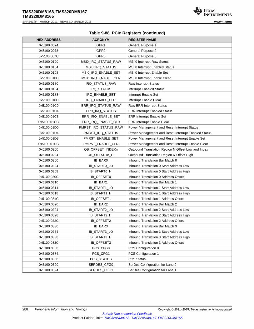
TMS320DM8168, TMS320DM8167TMS320DM8165SPRS614F –MARCH 2011–REVISED MARCH 2015 www.ti.com
Table 9-88. PCIe Registers (continued)HEX ADDRESS ACRONYM REGISTER NAME
0x5100 0074 GPR1 General Purpose 10x5100 0078 GPR2 General Purpose 20x5100 007C GPR3 General Purpose 30x5100 0100 MSI0_IRQ_STATUS_RAW MSI 0 Interrupt Raw Status0x5100 0104 MSI0_IRQ_STATUS MSI 0 Interrupt Enabled Status0x5100 0108 MSI0_IRQ_ENABLE_SET MSI 0 Interrupt Enable Set0x5100 010C MSI0_IRQ_ENABLE_CLR MSI 0 Interrupt Enable Clear0x5100 0180 IRQ_STATUS_RAW Raw Interrupt Status0x5100 0184 IRQ_STATUS Interrupt Enabled Status0x5100 0188 IRQ_ENABLE_SET Interrupt Enable Set0x5100 018C IRQ_ENABLE_CLR Interrupt Enable Clear0x5100 01C0 ERR_IRQ_STATUS_RAW Raw ERR Interrupt Status0x5100 01C4 ERR_IRQ_STATUS ERR Interrupt Enabled Status0x5100 01C8 ERR_IRQ_ENABLE_SET ERR Interrupt Enable Set0x5100 01CC ERR_IRQ_ENABLE_CLR ERR Interrupt Enable Clear0x5100 01D0 PMRST_IRQ_STATUS_RAW Power Management and Reset Interrupt Status0x5100 01D4 PMRST_IRQ_STATUS Power Management and Reset Interrupt Enabled Status0x5100 01D8 PMRST_ENABLE_SET Power Management and Reset Interrupt Enable Set0x5100 01DC PMRST_ENABLE_CLR Power Management and Reset Interrupt Enable Clear0x5100 0200 OB_OFFSET_INDEXn Outbound Translation Region N Offset Low and Index0x5100 0204 OB_OFFSETn_HI Outbound Translation Region N Offset High0x5100 0300 IB_BAR0 Inbound Translation Bar Match 00x5100 0304 IB_START0_LO Inbound Translation 0 Start Address Low0x5100 0308 IB_START0_HI Inbound Translation 0 Start Address High0x5100 030C IB_OFFSET0 Inbound Translation 0 Address Offset0x5100 0310 IB_BAR1 Inbound Translation Bar Match 10x5100 0314 IB_START1_LO Inbound Translation 1 Start Address Low0x5100 0318 IB_START1_HI Inbound Translation 1 Start Address High0x5100 031C IB_OFFSET1 Inbound Translation 1 Address Offset0x5100 0320 IB_BAR2 Inbound Translation Bar Match 20x5100 0324 IB_START2_LO Inbound Translation 2 Start Address Low0x5100 0328 IB_START2_HI Inbound Translation 2 Start Address High0x5100 032C IB_OFFSET2 Inbound Translation 2 Address Offset0x5100 0330 IB_BAR3 Inbound Translation Bar Match 30x5100 0334 IB_START3_LO Inbound Translation 3 Start Address Low0x5100 0338 IB_START3_HI Inbound Translation 3 Start Address High0x5100 033C IB_OFFSET3 Inbound Translation 3 Address Offset0x5100 0380 PCS_CFG0 PCS Configuration 00x5100 0384 PCS_CFG1 PCS Configuration 10x5100 0388 PCS_STATUS PCS Status0x5100 0390 SERDES_CFG0 SerDes Configuration for Lane 00x5100 0394 SERDES_CFG1 SerDes Configuration for Lane 1
288 Peripheral Information and Timings Copyright © 2011–2015, Texas Instruments IncorporatedSubmit Documentation Feedback
Product Folder Links: TMS320DM8168 TMS320DM8167 TMS320DM8165
TMS320DM8168, TMS320DM8167TMS320DM8165
www.ti.com SPRS614F –MARCH 2011–REVISED MARCH 2015
9.14.3 PCIe Electrical Data and TimingTexas Instruments (TI) has performed the simulation and system characterization to ensure that the PCIeperipheral meets all AC timing specifications as required by the PCI Express Base 2.0 Specification.Therefore, the AC timing specifications are not reproduced here. For more information on the AC timingspecifications, see Sections 4.3.3.5 and 4.3.4.4 of the PCI Express Base 2.0 Specification.
Copyright © 2011–2015, Texas Instruments Incorporated Peripheral Information and Timings 289Submit Documentation Feedback
Product Folder Links: TMS320DM8168 TMS320DM8167 TMS320DM8165
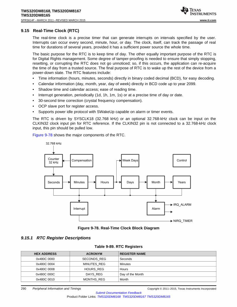
32.768 kHz
Counter32 kHz
Compensation Week Days Control
Seconds Minutes Hours Days Month Years
Interrupt Alarm
IRQ_ALARM
NIRQ_TIMER
TMS320DM8168, TMS320DM8167TMS320DM8165SPRS614F –MARCH 2011–REVISED MARCH 2015 www.ti.com
9.15 Real-Time Clock (RTC)The real-time clock is a precise timer that can generate interrupts on intervals specified by the user.Interrupts can occur every second, minute, hour, or day. The clock, itself, can track the passage of realtime for durations of several years, provided it has a sufficient power source the whole time.
The basic purpose for the RTC is to keep time of day. The other equally important purpose of the RTC isfor Digital Rights management. Some degree of tamper-proofing is needed to ensure that simply stopping,resetting, or corrupting the RTC does not go unnoticed; so, if this occurs, the application can re-acquirethe time of day from a trusted source. The final purpose of RTC is to wake up the rest of the device from apower-down state. The RTC features include:• Time information (hours, minutes, seconds) directly in binary coded decimal (BCD), for easy decoding.• Calendar information (day, month, year, day of week) directly in BCD code up to year 2099.• Shadow time and calendar access; ease of reading time.• Interrupt generation, periodically (1d, 1h, 1m, 1s) or at a precise time of day or date.• 30-second time correction (crystal frequency compensation).• OCP slave port for register access.• Supports power idle protocol with SWakeUp capable on alarm or timer events.
The RTC is driven by SYSCLK18 (32.768 kHz) or an optional 32.768-kHz clock can be input on theCLKIN32 clock input pin for RTC reference. If the CLKIN32 pin is not connected to a 32.768-kHz clockinput, this pin should be pulled low.
Figure 9-78 shows the major components of the RTC.
Figure 9-78. Real-Time Clock Block Diagram
9.15.1 RTC Register Descriptions
Table 9-89. RTC Registers
HEX ADDRESS ACRONYM REGISTER NAME0x480C 0000 SECONDS_REG Seconds0x480C 0004 MINUTES_REG Minutes0x480C 0008 HOURS_REG Hours0x480C 000C DAYS_REG Day of the Month0x480C 0010 MONTHS_REG Month
290 Peripheral Information and Timings Copyright © 2011–2015, Texas Instruments IncorporatedSubmit Documentation Feedback
Product Folder Links: TMS320DM8168 TMS320DM8167 TMS320DM8165

TMS320DM8168, TMS320DM8167TMS320DM8165
www.ti.com SPRS614F –MARCH 2011–REVISED MARCH 2015
Table 9-89. RTC Registers (continued)HEX ADDRESS ACRONYM REGISTER NAME
0x480C 0014 YEARS_REG Year0x480C 0018 WEEK_REG Day of the Week0x480C 0020 ALARM_SECONDS_REG Alarm Seconds0x480C 0024 ALARM_MINUTES_REG Alarm Minutes0x480C 0028 ALARM_HOURS_REG Alarm Hours0x480C 002C ALARM_DAYS_REG Alarm Days0x480C 0030 ALARM_MONTHS_REG Alarm Months0x480C 0034 ALARM_YEARS_REG Alarm Years0x480C 0040 RTC_CTRL_REG Control0x480C 0044 RTC_STATUS_REG Status0x480C 0048 RTC_INTERRUPTS_REG Interrupt Enable0x480C 004C RTC_COMP_LSB_REG Compensation (LSB)0x480C 0050 RTC_COMP_MSB_REG Compensation (MSB)0x480C 0054 RTC_OSC_REG Oscillator0x480C 0060 RTC_SCRATCH0_REG Scratch 0 (general-purpose)0x480C 0064 RTC_SCRATCH1_REG Scratch 1 (general-purpose)0x480C 0068 RTC_SCRATCH2_REG Scratch 2 (general-purpose)0x480C 006C KICK0 Kick 0 (write protect)0x480C 0070 KICK1 Kick 1 (write protect)0x480C 0074 RTC_REVISION Revision0x480C 0078 RTC_SYSCONFIG Clock Management Configuration0x480C 007A RTC_IRQWAKEEN_0 Wakeup Generation
Copyright © 2011–2015, Texas Instruments Incorporated Peripheral Information and Timings 291Submit Documentation Feedback
Product Folder Links: TMS320DM8168 TMS320DM8167 TMS320DM8165

TMS320DM8168, TMS320DM8167TMS320DM8165SPRS614F –MARCH 2011–REVISED MARCH 2015 www.ti.com
9.16 Secure Digital and Secure Digital Input Output (SD and SDIO)The device SD and SDIO Controller has following features:• Secure Digital (SD) memory card with Secure Data IO (SDIO)• Supports SDHC (SD high capacity)• SD and SDIO protocol support• Programmable clock frequency• 1024 byte read or write FIFO to lower system overhead• Slave DMA transfer capability• Full compliance with SD command and response sets, as defined in the SD physical layer specification
v2.00• Full compliance with SDIO command and response sets and interrupt and read-wait suspend-resume
operations, as defined in the SD part E1 specification v 2.00• Full compliance with SD host controller standard specification sets as defined in the SD card
specification part A2 v2.00.
For more detailed information on SD and SDIO, see the SD and SDIO chapter in the TMS320DM816xDaVinci Digital Media Processors Technical Reference Manual (literature number SPRUGX8).
9.16.1 SD and SDIO Peripheral Register Descriptions
Table 9-90. SD and SDIO Registers (1)
HEX ADDRESS ACRONYM REGISTER NAME0x4806 0000 SD_HL_REV IP Revision Identifier0x4806 0004 SD_HL_HWINFO Hardware Configuration0x4806 0010 SD_HL_SYSCONFIG Clock Management Configuration0x4806 0110 SD_SYSCONFIG System Configuration0x4806 0114 SD_SYSSTATUS System Status0x4806 0124 SD_CSRE Card status response error0x4806 0128 SD_SYSTEST System Test0x4806 012C SD_CON Configuration0x4806 0130 SD_PWCNT Power counter0x4806 0200 SD_SDMASA SDMA System address:0x4806 0204 SD_BLK Transfer Length Configuration0x4806 0208 SD_ARG Command argument0x4806 020C SD_CMD Command and transfer mode0x4806 0210 SD_RSP10 Command Response 0 and 10x4806 0214 SD_RSP32 Command Response 2 and 30x4806 0218 SD_RSP54 Command Response 4 and 50x4806 021C SD_RSP76 Command Response 6 and 70x4806 0220 SD_DATA Data0x4806 0224 SD_PSTATE Present state0x4806 0228 SD_HCTL Host Control0x4806 022C SD_SYSCTL SD system control0x4806 0230 SD_STAT Interrupt status0x4806 0234 SD_IE Interrupt SD enable0x4806 0238 SD_ISE0x4806 023C SD_AC12 Auto CMD12 Error Status0x4806 0240 SD_CAPA Capabilities0x4806 0248 SD_CUR_CAPA Maximum current capabilities
(1) SD and SDIO registers are limited to 32-bit data accesses; 16-bit and 8-bit accesses are not allowed and can corrupt register content.
292 Peripheral Information and Timings Copyright © 2011–2015, Texas Instruments IncorporatedSubmit Documentation Feedback
Product Folder Links: TMS320DM8168 TMS320DM8167 TMS320DM8165

TMS320DM8168, TMS320DM8167TMS320DM8165
www.ti.com SPRS614F –MARCH 2011–REVISED MARCH 2015
Table 9-90. SD and SDIO Registers(1) (continued)HEX ADDRESS ACRONYM REGISTER NAME
0x4806 0250 SD_FE Force Event0x4806 0254 SD_ADMAES ADMA Error Status0x4806 0258 SD_ADMASAL ADMA System address Low bits0x4806 025C SD_ADMASAH ADMA System address High bits0x4806 02FC SD_REV Versions
9.16.2 SD and SDIO Electrical Data and Timing
9.16.2.1 SD Identification and Standard SD Mode
Table 9-91. Timing Requirements for SD and SDIO—SD Identification and Standard SD Mode(see Figure 9-80, Figure 9-82)
NO. MIN MAX UNITSD Identification Mode
1 tsu(CMDV-CLKH) Setup time, SD_CMD valid before SD_CLK rising clock edge 1198.2 ns2 th(CLKH-CMDIV) Hold time, SD_CMD valid after SD_CLK rising clock edge 1249.0 ns
Standard SD Mode1 tsu(CMDV-CLKH) Setup time, SD_CMD valid before SD_CLK rising clock edge 4.1 ns2 th(CLKH-CMDIV) Hold time, SD_CMD valid after SD_CLK rising clock edge 1.9 ns3 tsu(DATV-CLKH) Setup time, SD_DATx valid before SD_CLK rising clock edge 4.1 ns4 th(CLKH-DATV) Hold time, SD_DATx valid after SD_CLK rising clock edge 1.9 ns
Table 9-92. Switching Characteristics Over Recommended Operating Conditions for SD and SDIO—SDIdentification and Standard SD Mode
(see Figure 9-79, Figure 9-80, Figure 9-81, Figure 9-82)NO. PARAMETER MIN MAX UNIT
SD Identification Modefop(CLKID) Identification mode frequency, SD_CLK 400 kHz
8tc(CLKID) Identification mode period, SD_CLK 2500.0 ns
13 td(CLKH-CMD) Delay time, SD_CLK rising clock edge to SD_CMD transition 6.5 2492.5 nsStandard SD Mode
fop(CLK) Operating frequency, SD_CLK 24 MHz7
tc(CLK) Operating period, SD_CLK 41.7 ns9 tw(CLKL) Pulse duration, SD_CLK low 0.45*P (1) 0.55*P (1) ns10 tw(CLKH) Pulse duration, SD_CLK high 0.45*P (1) 0.55*P (1) ns13 td(CLKH-CMD) Delay time, SD_CLK rising clock edge to SD_CMD transition 6.3 35.3 ns14 td(CLKH-DAT) Delay time, SD_CLK rising clock edge to SD_DATx transition 6.3 35.3 ns
(1) P = SD_CLK period.
9.16.2.2 High-Speed SD Mode
Table 9-93. Timing Requirements for SD and SDIO—High-Speed SD Mode(see Figure 9-80, Figure 9-82)
NO. MIN MAX UNIT1 tsu(CMDV-CLKH) Setup time, SD_CMD valid before SD_CLK rising clock edge 4.1 ns2 th(CLKH-CMDV) Hold time, SD_CMD valid after SD_CLK rising clock edge 1.9 ns3 tsu(DATV-CLKH) Setup time, SD_DATx valid before SD_CLK rising clock edge 4.1 ns4 th(CLKH-DATV) Hold time, SD_DATx valid after SD_CLK rising clock edge 1.9 ns
Copyright © 2011–2015, Texas Instruments Incorporated Peripheral Information and Timings 293Submit Documentation Feedback
Product Folder Links: TMS320DM8168 TMS320DM8167 TMS320DM8165

Start D0 D1 Dx End
7
SD_CLK
SD_DATx
910
4
3
4
3
START D0 D1 Dx END
7
SD_CLK
SD_DATx
14
10
9
14 14 14
START XMIT Valid Valid Valid END
7
SD_CLK
SD_CMD
109
1
2
START XMIT Valid Valid Valid END
7
SD_CLK
SD_CMD
13
10
9
13 13 13
TMS320DM8168, TMS320DM8167TMS320DM8165SPRS614F –MARCH 2011–REVISED MARCH 2015 www.ti.com
Table 9-94. Switching Characteristics Over Recommended Operating Conditions for SD and SDIO—High-Speed SD Mode
(see Figure 9-79, Figure 9-80, Figure 9-81, Figure 9-82)NO. PARAMETER MIN MAX UNIT
fop(CLK) Operating frequency, SD_CLK 48 MHz7
tc(CLK) Operating period: SD_CLK 20.8 nsfop(CLKID) Identification mode frequency, SD_CLK 400 kHz
8tc(CLKID) Identification mode period: SD_CLK 2500.0 ns
9 tw(CLKL) Pulse duration, SD_CLK low 0.5*P (1) ns10 tw(CLKH) Pulse duration, SD_CLK high 0.5*P (1) ns11 tr(CLK) Rise time, All Signals (10% to 90%) 2.2 ns12 tf(CLK) Fall time, All Signals (10% to 90%) 2.2 ns13 td(CLKL-CMD) Delay time, SD_CLK rising clock edge to SD_CMD transition 2.5 (2) 13.9 ns14 td(CLKL-DAT) Delay time, SD_CLK rising clock edge to SD_DATx transition 2.5 (2) 13.9 ns
(1) P = SD_CLK period.(2) Longer DATA and CMD PCB track routing than clock trace routing may be needed to meet SD device input hold time.
Figure 9-79. SD Host Command Timing
Figure 9-80. SD Card Response Timing
Figure 9-81. SD Host Write Timing
Figure 9-82. SD Host Read and Card CRC Status Timing
294 Peripheral Information and Timings Copyright © 2011–2015, Texas Instruments IncorporatedSubmit Documentation Feedback
Product Folder Links: TMS320DM8168 TMS320DM8167 TMS320DM8165

SATA Interface (Processor) SATA Connector
SATA_TXN
SATA_TXP
SATA_RXN
SATA_RXP
TX-
TX+
RX-
RX+
10 nF
10 nF
10 nF
10 nF
TMS320DM8168, TMS320DM8167TMS320DM8165
www.ti.com SPRS614F –MARCH 2011–REVISED MARCH 2015
9.17 Serial ATA Controller (SATA)The Serial ATA (SATA) peripheral provides a direct interface for up to two hard disk drives (SATA) andsupports the following features:• Serial ATA 1.5 Gbps and 3 Gbps speeds• Integrated PHY• Integrated Rx and Tx data buffers• Supports all SATA power management features• Hardware-assisted native command queuing (NCQ) for up to 32 entries• Supports port multiplier with command-based switching for connection to multiple hard disk drives• Activity LED support.
For more detailed information on the SATA, see the SATA chapter in the TMS320DM816x DaVinci DigitalMedia Processors Technical Reference Manual (literature number SPRUGX8).
9.17.1 SATA Interface Design Specifications
NOTEFor more information on PCB layout, see the DM816xx Easy CYG Package PCB EscapeRouting application report (literature number SPRABK6).
This section provides PCB design and layout specifications for the SATA interface. The design rulesconstrain PCB trace length, PCB trace skew, signal integrity, cross-talk, and signal timing. Simulation andsystem design work has been done to ensure the SATA interface requirements are met.
A standard 100-MHz differential clock source must be used for SATA operation (for details, seeSection 8.3.2).
9.17.1.1 SATA Interface Schematic
Figure 9-83 shows the data portion of the SATA interface schematic. The specific pin numbers can beobtained from Table 4-17, Serial ATA Terminal Functions.
Figure 9-83. SATA Interface High-Level Schematic
9.17.1.2 Compatible SATA Components and Modes
Table 9-95 shows the compatible SATA components and supported modes. Note that the only supportedconfiguration is an internal cable from the processor host to the SATA device.
Table 9-95. SATA Supported Modes
PARAMETER MIN MAX UNIT SUPPORTEDTransfer Rates 1.5 3.0 GbpseSATA - - - No
Copyright © 2011–2015, Texas Instruments Incorporated Peripheral Information and Timings 295Submit Documentation Feedback
Product Folder Links: TMS320DM8168 TMS320DM8167 TMS320DM8165

TMS320DM8168, TMS320DM8167TMS320DM8165SPRS614F –MARCH 2011–REVISED MARCH 2015 www.ti.com
Table 9-95. SATA Supported Modes (continued)PARAMETER MIN MAX UNIT SUPPORTED
xSATA - - - NoBackplane - - - NoInternal Cable - - - Yes
9.17.1.3 PCB Stackup Specifications
Table 9-96 shows the PCB stackup and feature sizes required for SATA.
Table 9-96. SATA PCB Stackup Specifications
PARAMETER MIN TYP MAX UNITPCB routing and plane layers 4 6 - LayersSignal routing layers 2 3 - LayersNumber of ground plane cuts allowed within SATA routing region - - 0 CutsNumber of layers between SATA routing region and reference ground plane - - 0 LayersPCB trace width, w - 4 - MilsPCB BGA escape via pad size - 20 - MilsPCB BGA escape via hole size - 10 MilsProcessor BGA pad size (1) 0.3 mm
(1) NSMD pad, per IPC-7351A BGA pad size guideline.
9.17.1.4 Routing Specifications
The SATA data signal traces must be routed to achieve 100 Ω (±20%) differential impedance and 60 Ω(±15%) single-ended impedance. The single-ended impedance is required because differential signals areextremely difficult to closely couple on PCBs and, therefore, single-ended impedance becomes important.60 Ω is chosen for the single-ended impedance to minimize problems caused by too low an impedance.
These impedances are impacted by trace width, trace spacing, distance to reference planes, and dielectricmaterial. Verify with a PCB design tool that the trace geometry for both data signal pairs results in asclose to 100 Ω differential impedance and 60 Ω single-ended impedance traces as possible. For bestaccuracy, work with your PCB fabricator to ensure this impedance is met.
Table 9-97 shows the routing specifications for the SATA data signals.
Table 9-97. SATA Routing Specifications
PARAMETER MIN TYP MAX UNITProcessor-to-SATA header trace length 10 (1) InchesNumber of stubs allowed on SATA traces (2) 0 StubsTX and RX pair differential impedance 80 100 120 ΩTX and RX single-ended impedance 51 60 69 ΩNumber of vias on each SATA trace 3 Vias (3)
SATA differential pair to any other trace spacing 2*DS (4)
(1) Beyond this, signal integrity may suffer.(2) In-line pads may be used for probing.(3) Vias must be used in pairs with their distance minimized.(4) DS = differential spacing of the SATA traces.
296 Peripheral Information and Timings Copyright © 2011–2015, Texas Instruments IncorporatedSubmit Documentation Feedback
Product Folder Links: TMS320DM8168 TMS320DM8167 TMS320DM8165
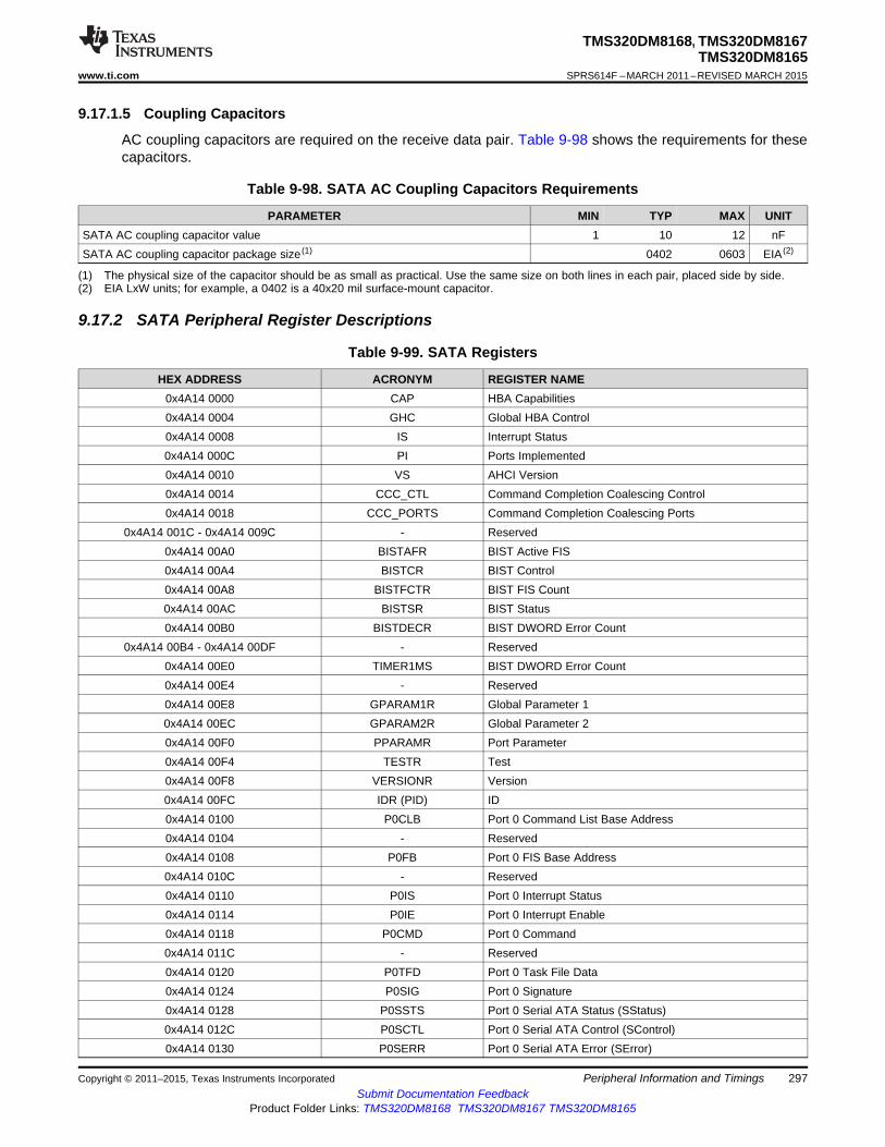
TMS320DM8168, TMS320DM8167TMS320DM8165
www.ti.com SPRS614F –MARCH 2011–REVISED MARCH 2015
9.17.1.5 Coupling Capacitors
AC coupling capacitors are required on the receive data pair. Table 9-98 shows the requirements for thesecapacitors.
Table 9-98. SATA AC Coupling Capacitors Requirements
PARAMETER MIN TYP MAX UNITSATA AC coupling capacitor value 1 10 12 nFSATA AC coupling capacitor package size (1) 0402 0603 EIA (2)
(1) The physical size of the capacitor should be as small as practical. Use the same size on both lines in each pair, placed side by side.(2) EIA LxW units; for example, a 0402 is a 40x20 mil surface-mount capacitor.
9.17.2 SATA Peripheral Register Descriptions
Table 9-99. SATA Registers
HEX ADDRESS ACRONYM REGISTER NAME0x4A14 0000 CAP HBA Capabilities0x4A14 0004 GHC Global HBA Control0x4A14 0008 IS Interrupt Status0x4A14 000C PI Ports Implemented0x4A14 0010 VS AHCI Version0x4A14 0014 CCC_CTL Command Completion Coalescing Control0x4A14 0018 CCC_PORTS Command Completion Coalescing Ports
0x4A14 001C - 0x4A14 009C - Reserved0x4A14 00A0 BISTAFR BIST Active FIS0x4A14 00A4 BISTCR BIST Control0x4A14 00A8 BISTFCTR BIST FIS Count0x4A14 00AC BISTSR BIST Status0x4A14 00B0 BISTDECR BIST DWORD Error Count
0x4A14 00B4 - 0x4A14 00DF - Reserved0x4A14 00E0 TIMER1MS BIST DWORD Error Count0x4A14 00E4 - Reserved0x4A14 00E8 GPARAM1R Global Parameter 10x4A14 00EC GPARAM2R Global Parameter 20x4A14 00F0 PPARAMR Port Parameter0x4A14 00F4 TESTR Test0x4A14 00F8 VERSIONR Version0x4A14 00FC IDR (PID) ID0x4A14 0100 P0CLB Port 0 Command List Base Address0x4A14 0104 - Reserved0x4A14 0108 P0FB Port 0 FIS Base Address0x4A14 010C - Reserved0x4A14 0110 P0IS Port 0 Interrupt Status0x4A14 0114 P0IE Port 0 Interrupt Enable0x4A14 0118 P0CMD Port 0 Command0x4A14 011C - Reserved0x4A14 0120 P0TFD Port 0 Task File Data0x4A14 0124 P0SIG Port 0 Signature0x4A14 0128 P0SSTS Port 0 Serial ATA Status (SStatus)0x4A14 012C P0SCTL Port 0 Serial ATA Control (SControl)0x4A14 0130 P0SERR Port 0 Serial ATA Error (SError)
Copyright © 2011–2015, Texas Instruments Incorporated Peripheral Information and Timings 297Submit Documentation Feedback
Product Folder Links: TMS320DM8168 TMS320DM8167 TMS320DM8165

TMS320DM8168, TMS320DM8167TMS320DM8165SPRS614F –MARCH 2011–REVISED MARCH 2015 www.ti.com
Table 9-99. SATA Registers (continued)HEX ADDRESS ACRONYM REGISTER NAME
0x4A14 0134 P0SACT Port 0 Serial ATA Active (SActive)0x4A14 0138 P0CI Port 0 Command Issue0x4A14 013C P0SNTF Port 0 Serial ATA Notification
0x4A14 0140 - 0x4A14 016C - Reserved0x4A14 0170 P0DMACR Port 0 DMA Control0x4A14 0174 - Reserved0x4A14 0178 P0PHYCR Port 0 PHY Control0x4A14 017C P0PHYSR Port 0 PHY Status0x4A14 0180 P1CLB Port 1 Command List Base Address0x4A14 0184 - Reserved0x4A14 0188 P1FB Port 1 FIS Base Address0x4A14 018C - Reserved0x4A14 0190 P1IS Port 1 Interrupt Status0x4A14 0194 P1IE Port 1 Interrupt Enable0x4A14 0198 P1CMD Port 1 Command0x4A14 019C - Reserved0x4A14 01A0 P1TFD Port 1 Task File Data0x4A14 01A4 P1SIG Port 1 Signature0x4A14 01A8 P1SSTS Port 1 Serial ATA Status (SStatus)0x4A14 01AC P1SCTL Port 1 Serial ATA Control (SControl)0x4A14 01B0 P1SERR Port 1 Serial ATA Error (SError)0x4A14 01B4 P1SACT Port 1 Serial ATA Active (SActive)0x4A14 01B8 P1CI Port 1 Command Issue0x4A14 01BC P1SNTF Port 1 Serial ATA Notification
0x4A14 01C0 - 0x4A14 01EC - Reserved0x4A14 01F0 P1DMACR Port 1 DMA Control0x4A14 01F4 - Reserved0x4A14 01F8 P1PHYCR Port 1 PHY Control0x4A14 01FC P1PHYSR Port 1 PHY Status0x4A14 1100 IDLE Idle and Standby Modes0x4A14 1104 PHYCFGR2 PHY Configuration 2
298 Peripheral Information and Timings Copyright © 2011–2015, Texas Instruments IncorporatedSubmit Documentation Feedback
Product Folder Links: TMS320DM8168 TMS320DM8167 TMS320DM8165

TMS320DM8168, TMS320DM8167TMS320DM8165
www.ti.com SPRS614F –MARCH 2011–REVISED MARCH 2015
9.18 Serial Peripheral Interface (SPI)The SPI is a high-speed synchronous serial input and output port that allows a serial bit stream ofprogrammed length (4 to 32 bits) to be shifted into and out of the device at a programmed bit-transfer rate.The SPI is normally used for communication between the device and external peripherals. Typicalapplications include an interface-to-external IO or peripheral expansion via devices such as shift registers,display drivers, SPI EEPROMs, and analog-to-digital converters (ADCs).
The SPI supports the following features:• Master and slave operation• Four chip selects for interfacing and control to up to four SPI slave devices and connection to a single
external master• 32-bit shift register• Buffered receive and transmit data register per channel (1 word deep), FIFO size is 64 bytes• Programmable SPI configuration per channel (clock definition, enable polarity and word width)• Supports one interrupt request and two DMA requests per channel.
For more detailed information on the SPI, see the SPI chapter in the TMS320DM816x DaVinci DigitalMedia Processors Technical Reference Manual (literature number SPRUGX8).
9.18.1 SPI Peripheral Register Descriptions
Table 9-100. SPI Registers
HEX ADDRESS ACRONYM REGISTER NAME0x4803 0000 - 0x4803 010C - RESERVED
0x4803 0110 MCSPI_SYSCONFIG SYSTEM CONFIGURATION0x4803 0114 MCSPI_SYSSTATUS SYSTEM STATUS0x4803 0118 MCSPI_IRQSTATUS INTERRUPT STATUS0x4803 011C MCSPI_IRQENABLE INTERRUPT ENABLE0x4803 0120 - RESERVED0x4803 0124 MCSPI_SYST SYSTEM TEST0x4803 0128 MCSPI_MODULCTRL MODULE CONTROL0x4803 012C MCSPI_CH0CONF CHANNEL 0 CONFIGURATION0x4803 0130 MCSPI_CH0STAT CHANNEL 0 STATUS0x4803 0134 MCSPI_CH0CTRL CHANNEL 0 CONTROL0x4803 0138 MCSPI_TX0 CHANNEL 0 TRANSMITTER0x4803 013C MCSPI_RX0 CHANNEL 0 RECEIVER0x4803 0140 MCSPI_CH1CONF CHANNEL 1 CONFIGURATION0x4803 0144 MCSPI_CH1STAT CHANNEL 1 STATUS0x4803 0148 MCSPI_CH1CTRL CHANNEL 1 CONTROL0x4803 014C MCSPI_TX1 CHANNEL 1 TRANSMITTER0x4803 0150 MCSPI_RX1 CHANNEL 1 RECEIVER0x4803 0154 MCSPI_CH2CONF CHANNEL 2 CONFIGURATION0x4803 0158 MCSPI_CH2STAT CHANNEL 2 STATUS0x4803 015C MCSPI_CH2CTRL CHANNEL 2 CONTROL0x4803 0160 MCSPI_TX2 CHANNEL 2 TRANSMITTER0x4803 0164 MCSPI_RX2 CHANNEL 2 RECEIVER0x4803 0168 MCSPI_CH3CONF CHANNEL 3 CONFIGURATION0x4803 016C MCSPI_CH3STAT CHANNEL 3 STATUS0x4803 0170 MCSPI_CH3CTRL CHANNEL 3 CONTROL0x4803 0174 MCSPI_TX3 CHANNEL 3 TRANSMITTER0x4803 0178 MCSPI_RX3 CHANNEL 3 RECEIVER
Copyright © 2011–2015, Texas Instruments Incorporated Peripheral Information and Timings 299Submit Documentation Feedback
Product Folder Links: TMS320DM8168 TMS320DM8167 TMS320DM8165

TMS320DM8168, TMS320DM8167TMS320DM8165SPRS614F –MARCH 2011–REVISED MARCH 2015 www.ti.com
Table 9-100. SPI Registers (continued)HEX ADDRESS ACRONYM REGISTER NAME
0x4803 017C MCSPI_XFERLEVEL TRANSFER LEVELS0x4803 0180 - 0x4803 01FF - RESERVED
300 Peripheral Information and Timings Copyright © 2011–2015, Texas Instruments IncorporatedSubmit Documentation Feedback
Product Folder Links: TMS320DM8168 TMS320DM8167 TMS320DM8165

TMS320DM8168, TMS320DM8167TMS320DM8165
www.ti.com SPRS614F –MARCH 2011–REVISED MARCH 2015
9.18.2 SPI Electrical Data and Timing
Table 9-101. Timing Requirements for SPI - Master Mode(see Figure 9-84 and Figure 9-85)NO. MIN MAX UNIT
MASTER: 1 LOAD AT A MAXIMUM OF 5 pF1 tc(SPICLK) Cycle time, SPI_CLK (1) (2) 20.8 (3) ns2 tw(SPICLKL) Pulse duration, SPI_CLK low (1) 0.5*P - 1 (4) ns3 tw(SPICLKH) Pulse duration, SPI_CLK high (1) 0.5*P - 1 (4) ns4 tsu(MISO-SPICLK) Setup time, SPI_D[x] valid before SPI_CLK active edge (1) 2.29 ns5 th(SPICLK-MISO) Hold time, SPI_D[x] valid after SPI_CLK active edge (1) 2.67 ns6 td(SPICLK-MOSI) Delay time, SPI_CLK active edge to SPI_D[x] transition (1) -3.57 3.57 ns7 td(SCS-MOSI) Delay time, SPI_SCS[x] active edge to SPI_D[x] transition 3.57 ns
MASTER_PHA0 (5) B-4.2 (6) nsDelay time, SPI_SCS[x] active to SPI_CLK8 td(SCS-SPICLK) first edge (1) MASTER_PHA1 (5) A-4.2 (7) nsMASTER_PHA0 (5) A-4.2 (7) nsDelay time, SPI_CLK last edge to SPI_SCS[x]9 td(SPICLK-SCS) inactive (1) MASTER_PHA1 (5) B-4.2 (6) ns
MASTER: UP TO 4 LOADS AT A MAXIMUM TOTAL OF 25 pF1 tc(SPICLK) Cycle time, SPI_CLK (1) (2) 41.7 (8) ns2 tw(SPICLKL) Pulse duration, SPI_CLK low (1) 0.5*P - 2 (4) ns3 tw(SPICLKH) Pulse duration, SPI_CLK high (1) 0.5*P - 2 (4) ns4 tsu(MISO-SPICLK) Setup time, SPI_D[x] valid before SPI_CLK active edge (1) 3.02 ns5 th(SPICLK-MISO) Hold time, SPI_D[x] valid after SPI_CLK active edge (1) 2.76 ns6 td(SPICLK-MOSI) Delay time, SPI_CLK active edge to SPI_D[x] transition (1) -4.62 4.62 ns7 td(SCS-MOSI) Delay time, SPI_SCS[x] active edge to SPI_D[x] transition 4.62 ns
MASTER_PHA0 (5) B-2.54 (6) nsDelay time, SPI_SCS[x] active to SPI_CLK8 td(SCS-SPICLK) first edge (1) MASTER_PHA1 (5) A-2.54 (7) nsMASTER_PHA0 (5) A-2.54 (7) nsDelay time, SPI_CLK last edge to SPI_SCS[x]9 td(SPICLK-SCS) inactive (1) MASTER_PHA1 (5) B-2.54 (6) ns
(1) This timing applies to all configurations regardless of SPI_CLK polarity and which clock edges are used to drive output data and captureinput data.
(2) Related to the SPI_CLK maximum frequency.(3) Maximum frequency = 48 MHz(4) P = SPICLK period.(5) SPI_CLK phase is programmable with the PHA bit of the SPI_CH(i)CONF register.(6) B = (TCS + 0.5) * TSPICLKREF * Fratio, where TCS is a bit field of the SPI_CH(i)CONF register and Fratio = Even ≥2.(7) When P = 20.8 ns, A = (TCS + 1) * TSPICLKREF, where TCS is a bit field of the SPI_CH(i)CONF register. When P > 20.8 ns, A = (TCS
+ 0.5) * Fratio * TSPICLKREF, where TCS is a bit field of the SPI_CH(i)CONF register.(8) Maximum frequency = 24 MHz
Copyright © 2011–2015, Texas Instruments Incorporated Peripheral Information and Timings 301Submit Documentation Feedback
Product Folder Links: TMS320DM8168 TMS320DM8167 TMS320DM8165

SPI_SCS[x] (Out)
SPI_SCLK (Out)
SPI_SCLK (Out)
SPI_D[x] (Out) Bit n-1 Bit n-2 Bit n-3 Bit n-4 Bit 0
PHA=0
EPOL=1
POL=0
POL=1
8 9
3
7 6
2
1
2
3
1
6
SPI_SCS[x] (Out)
SPI_SCLK (Out)
SPI_SCLK (Out)
SPI_D[x] (Out) Bit n-1 Bit n-2 Bit n-3 Bit 1 Bit 0
PHA=1
EPOL=1
POL=0
POL=1
8 9
3
6 6
2
1
2
3
1
6 6
TMS320DM8168, TMS320DM8167TMS320DM8165SPRS614F –MARCH 2011–REVISED MARCH 2015 www.ti.com
Figure 9-84. SPI Master Mode Transmit Timing
302 Peripheral Information and Timings Copyright © 2011–2015, Texas Instruments IncorporatedSubmit Documentation Feedback
Product Folder Links: TMS320DM8168 TMS320DM8167 TMS320DM8165

SPI_SCS[x] (Out)
SPI_SCLK (Out)
SPI_SCLK (Out)
SPI_D[x] (In) Bit n-1 Bit n-2 Bit n-3 Bit n-4 Bit 0
PHA=0
EPOL=1
POL=0
POL=1
8 9
3
4
2
1
2
3
5
SPI_SCS[x] (Out)
SPI_SCLK (Out)
SPI_SCLK (Out)
SPI_D[x] (In) Bit n-1 Bit n-2 Bit n-3 Bit 1 Bit 0
PHA=1
EPOL=1
POL=0
POL=1
8 9
3
2
1
2
3
1
4
5
4
5 5
4
1
TMS320DM8168, TMS320DM8167TMS320DM8165
www.ti.com SPRS614F –MARCH 2011–REVISED MARCH 2015
Figure 9-85. SPI Master Mode Receive Timing
Table 9-102. Timing Requirements for SPI - Slave Mode(see Figure 9-86 and Figure 9-87)
NO. MIN MAX UNIT1 tc(SPICLK) Cycle time, SPI_CLK (1) (2) 62.5 (3) ns2 tw(SPICLKL) Pulse duration, SPI_CLK low (1) 0.5*P - 3 (4) ns3 tw(SPICLKH) Pulse duration, SPI_CLK high (1) 0.5*P - 3 (4) ns4 tsu(MOSI-SPICLK) Setup time, SPI_D[x] valid before SPI_CLK active edge (1) 12.92 ns5 th(SPICLK-MOSI) Hold time, SPI_D[x] valid after SPI_CLK active edge (1) 12.92 ns6 td(SPICLK-MISO) Delay time, SPI_CLK active edge to SPI_D[x] transition (1) -4.00 17.1 ns
Delay time, SPI_SCS[x] active edge to SPI_D[x]7 td(SCS-MISO) 17.1 nstransition (5)
8 tsu(SCS-SPICLK) Setup time, SPI_SCS[x] valid before SPI_CLK first edge (1) 12.92 ns9 th(SPICLK-SCS) Hold time, SPI_SCS[x] valid after SPI_CLK last edge (1) 12.92 ns
(1) This timing applies to all configurations regardless of SPI_CLK polarity and which clock edges are used to drive output data and captureinput data.
(2) Related to the input maximum frequency supported by the SPI module.(3) Maximum frequency = 16 MHz(4) P = SPICLK period.(5) PHA = 0; SPI_CLK phase is programmable with the PHA bit of the SPI_CH(i)CONF register.
Copyright © 2011–2015, Texas Instruments Incorporated Peripheral Information and Timings 303Submit Documentation Feedback
Product Folder Links: TMS320DM8168 TMS320DM8167 TMS320DM8165

SPI_SCS[x] (In)
SPI_SCLK (In)
SPI_SCLK (In)
SPI_D[x] (Out) Bit n-1 Bit n-2 Bit n-3 Bit n-4 Bit 0
PHA=0
EPOL=1
POL=0
POL=1
8
3
76
2
1
2
1
SPI_SCS[x] (In)
SPI_SCLK (In)
SPI_SCLK (In)
SPI_D[x] (Out) Bit n-1 Bit n-2 Bit n-3 Bit 1 Bit 0
PHA=1
EPOL=1
POL=0
POL=1
8
3
6 6
2
1
2
3
1
6 6
9
6
9
3
TMS320DM8168, TMS320DM8167TMS320DM8165SPRS614F –MARCH 2011–REVISED MARCH 2015 www.ti.com
Figure 9-86. SPI Slave Mode Transmit Timing
304 Peripheral Information and Timings Copyright © 2011–2015, Texas Instruments IncorporatedSubmit Documentation Feedback
Product Folder Links: TMS320DM8168 TMS320DM8167 TMS320DM8165
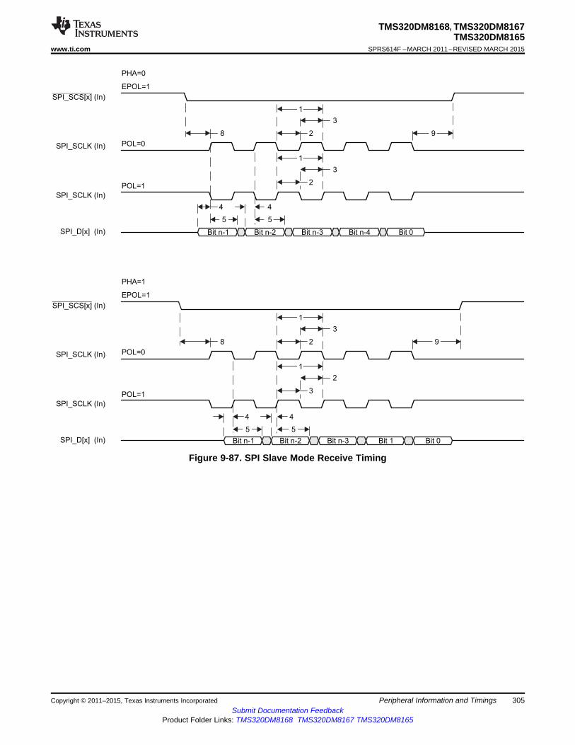
SPI_SCS[x] (In)
SPI_SCLK (In)
SPI_SCLK (In)
SPI_D[x] (In) Bit n-1 Bit n-2 Bit n-3 Bit n-4 Bit 0
PHA=0
EPOL=1
POL=0
POL=1
8
3
4
2
1
3
2
5
SPI_SCS[x] (In)
SPI_SCLK (In)
SPI_SCLK (In)
SPI_D[x] (In) Bit n-1 Bit n-2 Bit n-3 Bit 1 Bit 0
PHA=1
EPOL=1
POL=0
POL=1
8
3
2
1
2
3
1
4
5
4
5 5
4
9
1
9
TMS320DM8168, TMS320DM8167TMS320DM8165
www.ti.com SPRS614F –MARCH 2011–REVISED MARCH 2015
Figure 9-87. SPI Slave Mode Receive Timing
Copyright © 2011–2015, Texas Instruments Incorporated Peripheral Information and Timings 305Submit Documentation Feedback
Product Folder Links: TMS320DM8168 TMS320DM8167 TMS320DM8165
TMS320DM8168, TMS320DM8167TMS320DM8165SPRS614F –MARCH 2011–REVISED MARCH 2015 www.ti.com
9.19 TimersThe device has seven 32-bit general-purpose (GP) timers that have the following features:• Timers 1-3 are for software use and do not have an external connection• Dedicated input trigger for capture mode and dedicated output trigger or pulse width modulation
(PWM) signal• Interrupts generated on overflow, compare, and capture• Free-running 32-bit upward counter• Supported modes:
– Compare and capture modes– Auto-reload mode– Start-stop mode
• Timer[7:1] functional clock is sourced from either the 27-MHz system clock, 32.768-kHz RTC clock orthe TCLKIN external timer input clock, as selected within the PRCM
• On-the-fly read and write register (while counting)• Generates interrupts to the ARM and DSP CPUs.
The device has one system watchdog timer that has the following features:• Free-running 32-bit upward counter• On-the-fly read and write register (while counting)• Reset upon occurrence of a timer overflow condition• Two possible clock sources:
– Internal 32.768-kHz clock derived from 27-MHz system clock.– External clock input on the CLKIN32 input pin.
The watchdog timer is used to provide a recovery mechanism for the device in the event of a faultcondition, such as a non-exiting code loop.
For more detailed information, see the Timers chapter in the TMS320DM816x DaVinci Digital MediaProcessors Technical Reference Manual (literature number SPRUGX8).
9.19.1 Timer Peripheral Register Descriptions
Table 9-103. Timer1-7 Registers (1)
TIMER1 HEX TIMER2 HEX TIMER3 HEX TIMER4 HEX TIMER5 HEX TIMER6 HEX TIMER7 HEX ACRONYM REGISTER NAMEADDRESS ADDRESS ADDRESS ADDRESS ADDRESS ADDRESS ADDRESS
0x4802 E000 0x4804 0000 0x4804 2000 0x4804 4000 0x4804 6000 0x4804 8000 0x4804 A000 TIDR Identification
0x4802 E010 0x4804 0010 0x4804 2010 0x4804 4010 0x4804 6010 0x4804 8010 0x4804 A010 TIOCP_CFG Timer OCPConfiguration
0x4802 E020 0x4804 0020 0x4804 2020 0x4804 4020 0x4804 6020 0x4804 8020 0x4804 A020 IRQ_EOI Timer IRQ End-Of-Interrupt
0x4802 E024 0x4804 0024 0x4804 2024 0x4804 4024 0x4804 6024 0x4804 8024 0x4804 A024 IRQSTATUS_ Timer IRQSTATUSRAW Raw
0x4802 E028 0x4804 0028 0x4804 2028 0x4804 4028 0x4804 6028 0x4804 8028 0x4804 A028 IRQSTATUS Timer IRQSTATUS
0x4802 E02C 0x4804 002C 0x4804 202C 0x4804 402C 0x4804 602C 0x4804 802C 0x4804 A02C IRQSTATUS_ Timer IRQENABLESET Set
0x4802 E030 0x4804 0030 0x4804 2030 0x4804 4030 0x4804 6030 0x4804 8030 0x4804 A030 IRQSTATUS_ Timer IRQENABLECLR Clear
0x4802 E034 0x4804 0034 0x4804 2034 0x4804 4034 0x4804 6034 0x4804 8034 0x4804 A034 IRQWAKEEN Timer IRQ WakeupEnable
0x4802 E038 0x4804 0038 0x4804 2038 0x4804 4038 0x4804 6038 0x4804 8038 0x4804 A038 TCLR Timer Control
0x4802 E03C 0x4804 003C 0x4804 203C 0x4804 403C 0x4804 603C 0x4804 803C 0x4804 A03C TCRR Timer Counter
0x4802 E040 0x4804 0040 0x4804 2040 0x4804 4040 0x4804 6040 0x4804 8040 0x4804 A040 TLDR Timer Load
0x4802 E044 0x4804 0044 0x4804 2044 0x4804 4044 0x4804 6044 0x4804 8044 0x4804 A044 TTGR Timer Trigger
(1) All Timer registers are: 32-bit register accessible in 16-bit mode and use little-endian addressing.
306 Peripheral Information and Timings Copyright © 2011–2015, Texas Instruments IncorporatedSubmit Documentation Feedback
Product Folder Links: TMS320DM8168 TMS320DM8167 TMS320DM8165

TMS320DM8168, TMS320DM8167TMS320DM8165
www.ti.com SPRS614F –MARCH 2011–REVISED MARCH 2015
Table 9-103. Timer1-7 Registers(1) (continued)TIMER1 HEX TIMER2 HEX TIMER3 HEX TIMER4 HEX TIMER5 HEX TIMER6 HEX TIMER7 HEX ACRONYM REGISTER NAMEADDRESS ADDRESS ADDRESS ADDRESS ADDRESS ADDRESS ADDRESS
0x4802 E048 0x4804 0048 0x4804 2048 0x4804 4048 0x4804 6048 0x4804 8048 0x4804 A048 TWPS Timer Write PostedStatus
0x4802 E04C 0x4804 004C 0x4804 204C 0x4804 404C 0x4804 604C 0x4804 804C 0x4804 A04C TMAR Timer Match
0x4802 E050 0x4804 0050 0x4804 2050 0x4804 4050 0x4804 6050 0x4804 8050 0x4804 A050 TCAR1 Timer Capture
0x4802 E054 0x4804 0054 0x4804 2054 0x4804 4054 0x4804 6054 0x4804 8054 0x4804 A054 TSICR Timer SynchronousInterface Control
0x4802 E058 0x4804 0058 0x4804 2058 0x4804 4058 0x4804 6058 0x4804 8058 0x4804 A058 TCAR2 Timer Capture
Table 9-104. Watchdog Timer Registers
HEX ADDRESS ACRONYM REGISTER NAME0x480C 2000 WIDR IP Revision Identifier0x480C 2010 WDSC OCP interface parameters0x480C 2014 WDST Status information0x480C 2018 WISR Interrupt events pending0x480C 201C WIER Interrupt events control0x480C 2020 WWER Wakeup events control0x480C 2024 WCLR Counter prescaler control0x480C 2028 WCRR Internal counter value0x480C 202C WLDR Timer load value0x480C 2030 WTGR Watchdog counter reload0x480C 2034 WWPS Write posting bits0x480C 2044 WDLY Event detection delay value0x480C 2048 WSPR Start-stop value0x480C 2050 WIRQEOI Software End Of Interrupt0x480C 2054 WIRQSTATRAW IRQ unmasked status0x480C 2058 WIRQSTAT IRQ masked status0x480C 205C WIRQENSET IRQ enable0x480C 2060 WIRQENCLR IRQ enable clear0x480C 2064 WIRQWAKEEN IRQ wakeup events control
Copyright © 2011–2015, Texas Instruments Incorporated Peripheral Information and Timings 307Submit Documentation Feedback
Product Folder Links: TMS320DM8168 TMS320DM8167 TMS320DM8165
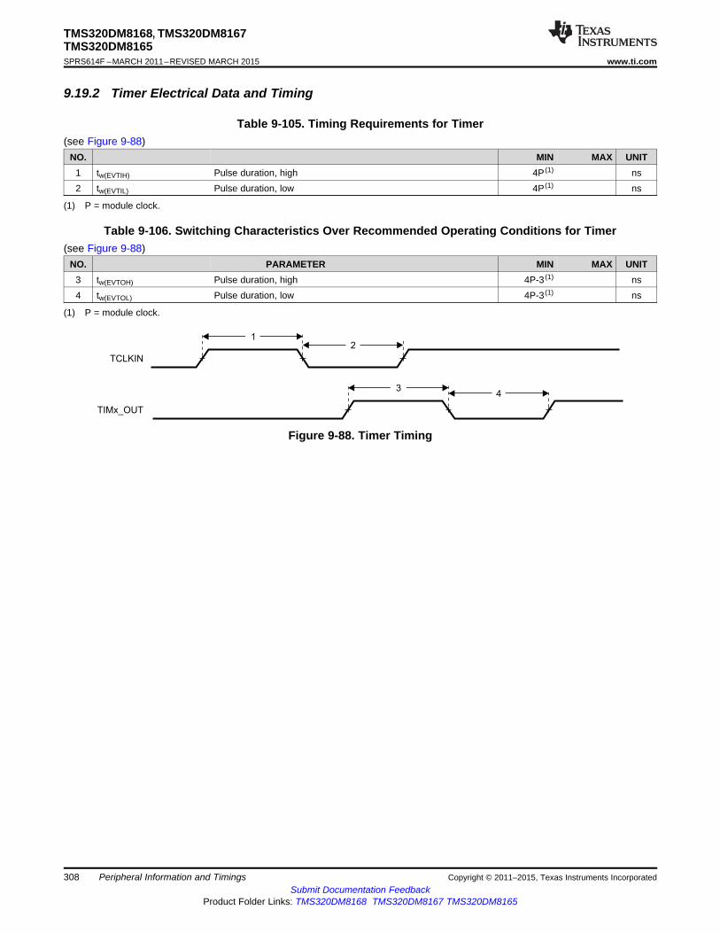
TCLKIN
TIMx_OUT
12
34
TMS320DM8168, TMS320DM8167TMS320DM8165SPRS614F –MARCH 2011–REVISED MARCH 2015 www.ti.com
9.19.2 Timer Electrical Data and Timing
Table 9-105. Timing Requirements for Timer(see Figure 9-88)
NO. MIN MAX UNIT1 tw(EVTIH) Pulse duration, high 4P (1) ns2 tw(EVTIL) Pulse duration, low 4P (1) ns
(1) P = module clock.
Table 9-106. Switching Characteristics Over Recommended Operating Conditions for Timer(see Figure 9-88)
NO. PARAMETER MIN MAX UNIT3 tw(EVTOH) Pulse duration, high 4P-3 (1) ns4 tw(EVTOL) Pulse duration, low 4P-3 (1) ns
(1) P = module clock.
Figure 9-88. Timer Timing
308 Peripheral Information and Timings Copyright © 2011–2015, Texas Instruments IncorporatedSubmit Documentation Feedback
Product Folder Links: TMS320DM8168 TMS320DM8167 TMS320DM8165
TMS320DM8168, TMS320DM8167TMS320DM8165
www.ti.com SPRS614F –MARCH 2011–REVISED MARCH 2015
9.20 Universal Asynchronous Receiver and Transmitter (UART)The UART performs serial-to-parallel conversions on data received from a peripheral device and parallel-to-serial conversion on data received from the CPU. The device provides up to three UART peripheralinterfaces, depending on the selected pin multiplexing.
Each UART has the following features:• Selectable UART, IrDA (SIR, MIR) and CIR modes• Dual 64-entry FIFOs for received and transmitted data payload• Programmable and selectable transmit and receive FIFO trigger levels for DMA and interrupt
generation• Baud-rate generation based upon programmable divisors N (N=1…16384)• Two DMA requests and one interrupt request to the system• Can connect to any RS-232 compliant device.
UART functions include:• Baud-rate up to 3.6 Mbps• Programmable serial interfaces characteristics
– 5, 6, 7, or 8-bit characters– Even, odd, or no parity-bit generation and detection– 1, 1.5, or 2 stop-bit generation– Flow control: hardware (RTS and CTS) or software (XON and XOFF)
• Additional modem control functions (UART0_DTR, UART0_DSR, UART0_DCD, and UART0_RIN) forUART0 only; UART1 and UART2 do not support full-flow control signaling.
IR-IrDA functions include:• Support of IrDA 1.4 slow infrared (SIR, baud-rate up to 115.2 Kbps), medium infrared (MIR, baud-rate
up to 1.152 Mbps) and fast infrared (FIR baud-rate up to 4.0 Mbps) communications• Supports framing error, cyclic redundancy check (CRC) error, illegal symbol (FIR), and abort pattern
(SIR, MIR) detection• 8-entry status FIFO (with selectable trigger levels) available to monitor frame length and frame errors.
IR-CIR functions include:• Consumer infrared (CIR) remote control mode with programmable data encoding• Free data format (supports any remote control private standards)• Selectable bit rate and configurable carrier frequency.
For more detailed information on the UART peripheral, see the UART chapter in the TMS320DM816xDaVinci Digital Media Processors Technical Reference Manual (literature number SPRUGX8).
Copyright © 2011–2015, Texas Instruments Incorporated Peripheral Information and Timings 309Submit Documentation Feedback
Product Folder Links: TMS320DM8168 TMS320DM8167 TMS320DM8165

TMS320DM8168, TMS320DM8167TMS320DM8165SPRS614F –MARCH 2011–REVISED MARCH 2015 www.ti.com
9.20.1 UART Peripheral Register DescriptionsTable 9-107 lists the UART register name summary. Table 9-108 shows the UART registers along withtheir configuration requirements.
Table 9-107. UART Register Summary
ACRONYM REGISTER NAME ACRONYM REGISTER NAMERHR Receive Holding RXFLH Receive Frame Length HighTHR Transmit Holding BLR BOF ControlIER Interrupt Enable ACREG Auxilliary ControlIIR Interrupt Identification SCR Supplementary Control
FCR FIFO Control SSR Supplementary StatusLCR Line Control EBLR BOF LengthMCR Modem Control MVR Module VersionLSR Line Status SYSC System ConfigurationMSR Modem Status SYSS System StatusSPR Scratchpad WER Wake-up EnableTCR Transmission Control CFPS Carrier Frequency PrescalerTLR Trigger Level DLL Divisor Latch Low
MDR1 Mode Definition 1 DLH Divisor Latch HighMDR2 Mode Definition 2 UASR UART Autobauding StatusSFLSR Status FIFO Line Status EFR Enhanced Feature
RESUME Resume XON1 UART XON1 CharacterSFREGL Status FIFO Low XON2 UART XON2 CharacterSFREGH Status FIFO High XOFF1 UART XOFF1 Character
TXFLL Transmit Frame Length Low XOFF2 UART XOFF2 CharacterTXFLH Transmit Frame Length High ADDR1 IrDA Address 1RXFLL Receive Frame Length Low ADDR2 IrDA Address 2
Table 9-108. UART Registers Configuration Requirements (1) (2) (3)
REGISTERUART0 HEX UART1 HEX UART2 HEX LCR[7] = 1 and LCR[7:0]LCR[7] = 0 LCR[7:0] = 0xBFADDRESS ADDRESS ADDRESS ≠ 0xBF
READ WRITE READ WRITE READ WRITE0x4802 0000 0x4802 2000 0x4802 4000 RHR THR DLL DLL DLL DLL0x4802 0004 0x4802 2004 0x4802 4004 IER IER DLH DLH DLH DLH0x4802 0008 0x4802 2008 0x4802 4008 IIR FCR IIR FCR EFR EFR0x4802 000C 0x4802 200C 0x4802 400C LCR LCR LCR LCR LCR LCR0x4802 0010 0x4802 2010 0x4802 4010 MCR MCR MCR MCR XON1 or XON1 or
ADDR1 ADDR10x4802 0014 0x4802 2014 0x4802 4014 LSR - LSR - XON2 or XON2 or
ADDR2 ADDR20x4802 0018 0x4802 2018 0x4802 4018 MSR or TCR MSR or TCR XOFF1 or XOFF1 or
TCR TCR TCR TCR0x4802 001C 0x4802 201C 0x4802 401C SPR orTLR SPR orTLR SPR or TLR SPR orTLR XOFF2 or XOFF2 or
TLR TLR0x4802 0020 0x4802 2020 0x4802 4020 MDR1 MDR1 MDR1 MDR1 MDR1 MDR10x4802 0024 0x4802 2024 0x4802 4024 MDR2 MDR2 MDR2 MDR2 MDR2 MDR20x4802 0028 0x4802 2028 0x4802 4028 SFLSR TXFLL SFLSR TXFLL SFLSR TXFLL
(1) The transmission control register (TCR) and the trigger level register (TLR) are accessible only when EFR[4]=1 and MCR[6]=1.(2) MCR[7:5] and FCR[5:4] can only be written when EFR[4]=1.(3) In UART modes, IER[7:4] can only be written when EFR[4]=1. In IrDA and CIR modes, EFR[4] has no impact on the access to IER[7:4].
310 Peripheral Information and Timings Copyright © 2011–2015, Texas Instruments IncorporatedSubmit Documentation Feedback
Product Folder Links: TMS320DM8168 TMS320DM8167 TMS320DM8165
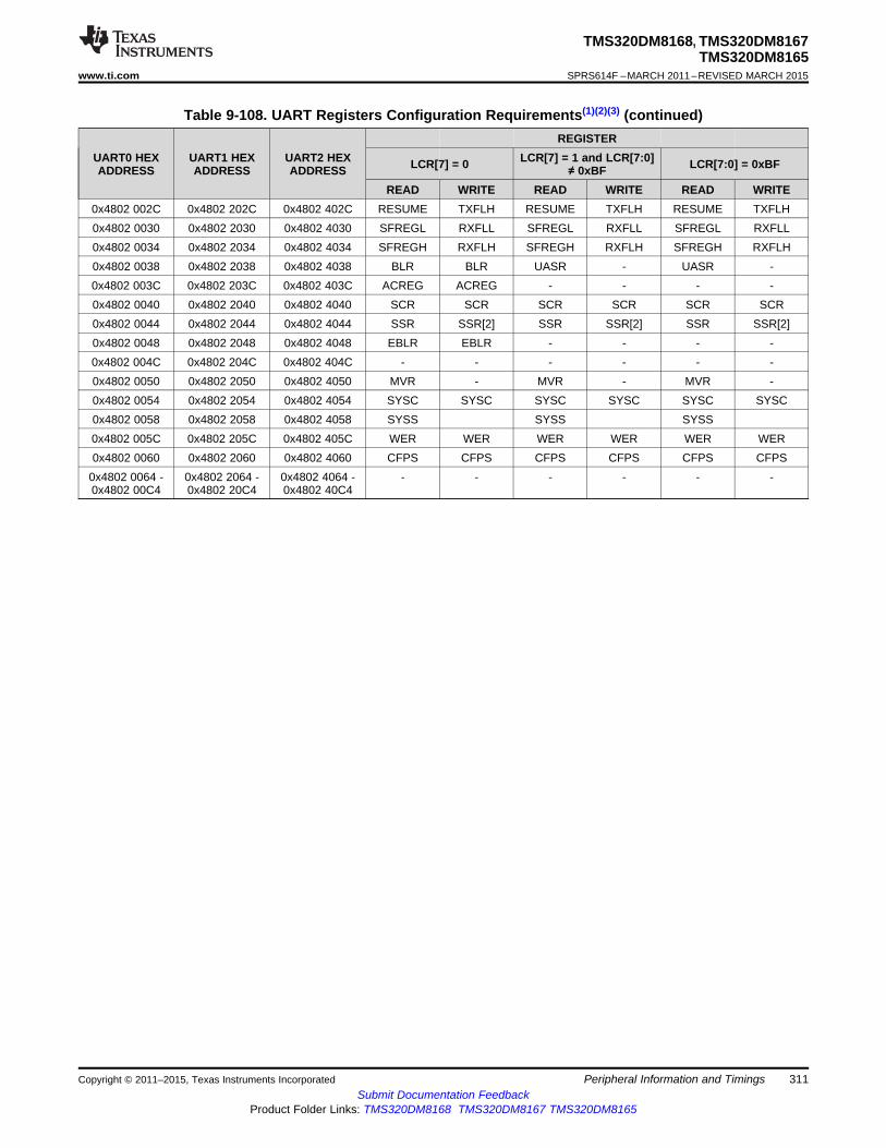
TMS320DM8168, TMS320DM8167TMS320DM8165
www.ti.com SPRS614F –MARCH 2011–REVISED MARCH 2015
Table 9-108. UART Registers Configuration Requirements(1)(2)(3) (continued)REGISTER
UART0 HEX UART1 HEX UART2 HEX LCR[7] = 1 and LCR[7:0]LCR[7] = 0 LCR[7:0] = 0xBFADDRESS ADDRESS ADDRESS ≠ 0xBFREAD WRITE READ WRITE READ WRITE
0x4802 002C 0x4802 202C 0x4802 402C RESUME TXFLH RESUME TXFLH RESUME TXFLH0x4802 0030 0x4802 2030 0x4802 4030 SFREGL RXFLL SFREGL RXFLL SFREGL RXFLL0x4802 0034 0x4802 2034 0x4802 4034 SFREGH RXFLH SFREGH RXFLH SFREGH RXFLH0x4802 0038 0x4802 2038 0x4802 4038 BLR BLR UASR - UASR -0x4802 003C 0x4802 203C 0x4802 403C ACREG ACREG - - - -0x4802 0040 0x4802 2040 0x4802 4040 SCR SCR SCR SCR SCR SCR0x4802 0044 0x4802 2044 0x4802 4044 SSR SSR[2] SSR SSR[2] SSR SSR[2]0x4802 0048 0x4802 2048 0x4802 4048 EBLR EBLR - - - -0x4802 004C 0x4802 204C 0x4802 404C - - - - - -0x4802 0050 0x4802 2050 0x4802 4050 MVR - MVR - MVR -0x4802 0054 0x4802 2054 0x4802 4054 SYSC SYSC SYSC SYSC SYSC SYSC0x4802 0058 0x4802 2058 0x4802 4058 SYSS SYSS SYSS0x4802 005C 0x4802 205C 0x4802 405C WER WER WER WER WER WER0x4802 0060 0x4802 2060 0x4802 4060 CFPS CFPS CFPS CFPS CFPS CFPS
0x4802 0064 - 0x4802 2064 - 0x4802 4064 - - - - - - -0x4802 00C4 0x4802 20C4 0x4802 40C4
Copyright © 2011–2015, Texas Instruments Incorporated Peripheral Information and Timings 311Submit Documentation Feedback
Product Folder Links: TMS320DM8168 TMS320DM8167 TMS320DM8165

3
2
Start
Bit
Data Bits
UARTx_TXD
5
Data Bits
Bit
Start
4
UARTx_RXD
TMS320DM8168, TMS320DM8167TMS320DM8165SPRS614F –MARCH 2011–REVISED MARCH 2015 www.ti.com
9.20.2 UART Electrical Data and Timing
Table 9-109. Timing Requirements for UART(see Figure 9-89)
NO. MIN MAX UNIT4 tw(RX) Pulse width, receive data bit, 15 pF, 30 pF, 100 pF high or low 0.96U (1) 1.05U (1) ns5 tw(CTS) Pulse width, receive start bit, 15 pF, 30 pF, 100 pF high or low 0.96U (1) 1.05U (1) ns
td(RTS-TX) Delay time, transmit start bit to transmit data P (2) nstd(CTS-TX) Delay time, receive start bit to transmit data P (2) ns
(1) U = UART baud time = 1/programmed baud rate.(2) P = clock period of the reference clock (FCLK, usually 48 MHz).
Table 9-110. Switching Characteristics Over Recommended Operating Conditions for UART(see Figure 9-89)
NO. PARAMETER MIN MAX UNIT15 pF 5
f(baud) Maximum programmable baud rate 30 pF 0.23 MHz100 pF 0.115
2 tw(TX) Pulse width, transmit data bit, 15 pF, 30 pF, 100 pF high or low U - 2 (1) U + 2 (1) ns3 tw(RTS) Pulse width, transmit start bit, 15 pF, 30 pF, 100 pF high or low U - 2 (1) U + 2 (1) ns
(1) U = UART baud time = 1/programmed baud rate.
Figure 9-89. UART Timing
312 Peripheral Information and Timings Copyright © 2011–2015, Texas Instruments IncorporatedSubmit Documentation Feedback
Product Folder Links: TMS320DM8168 TMS320DM8167 TMS320DM8165

TMS320DM8168, TMS320DM8167TMS320DM8165
www.ti.com SPRS614F –MARCH 2011–REVISED MARCH 2015
9.21 Universal Serial Bus (USB2.0)The device includes two USB2.0 modules which support the Universal Serial Bus Specification Revision2.0. The following are some of the major USB features that are supported:• USB 2.0 peripheral at high speed (HS: 480 Mbps) and full speed (FS: 12 Mbps)• USB 2.0 host at HS, FS, and low speed (LS: 1.5 Mbps)• Each endpoint (other than endpoint 0, control only) can support all transfer modes (control, bulk,
interrupt, and isochronous)• Supports high-bandwidth ISO mode• Supports 16 Transmit (TX) and 16 Receive (RX) endpoints including endpoint 0• FIFO RAM - 32K endpoint - Programmable size• Includes two integrated PHYs; requires a low-jitter 24-MHz source clock for its PLL• RNDIS-like mode for terminating RNDIS-type protocols without using short-packet termination for
support of MSC applications.
The USB2.0 modules do not support the following features:• On-chip charge pump (VBUS power must be generated external to the device)• RNDIS mode acceleration for USB sizes that are not multiples of 64 bytes• Endpoint max USB packet sizes that do not conform to the USB2.0 spec (for FS and LS: 8, 16, 32, 64,
and 1023 are defined; for HS: 64, 128, 512, and 1024 are defined).
For more detailed information on the USB2.0 peripheral, see the USB2.0 chapter in the TMS320DM816xDaVinci Digital Media Processors Technical Reference Manual (literature number SPRUGX8). Fordetailed information on USB board design and layout guidelines, see the USB 2.0 Board Design andLayout Guidelines application report (literature number SPRAAR7). For general information on PCBlayout, see the DM816xx Easy CYG Package PCB Escape Routing application report (literature numberSPRABK6).
9.21.1 USB2.0 Peripheral Register Descriptions
Table 9-111. USB2.0 Submodules
SUBMODULE SUBMODULE NAMEADDRESS OFFSET0x0000 USBSS registers0x1000 USB0 controller registers0x1800 USB1 controller registers0x2000 CPPI DMA controller registers0x3000 CPPI DMA scheduler registers0x4000 CPPI DMA Queue Manager registers
Table 9-112. USB Subsystem (USBSS) Registers (1)
HEX ADDRESS ACRONYM REGISTER NAME0x4740 0000 REVREG USBSS REVISION
0x4740 0004 - 0x4740 000C - Reserved0x4740 0010 SYSCONFIG USBSS SYSCONFIG
0x4740 0014 - 0x4740 001C - Reserved0x4740 0020 EOI USBSS IRQ_EOI0x4740 0024 IRQSTATRAW USBSS IRQ_STATUS_RAW0x4740 0028 IRQSTAT USBSS IRQ_STATUS
(1) USBSS registers contain the registers that are used to control at the global level and apply to all submodules.
Copyright © 2011–2015, Texas Instruments Incorporated Peripheral Information and Timings 313Submit Documentation Feedback
Product Folder Links: TMS320DM8168 TMS320DM8167 TMS320DM8165

TMS320DM8168, TMS320DM8167TMS320DM8165SPRS614F –MARCH 2011–REVISED MARCH 2015 www.ti.com
Table 9-112. USB Subsystem (USBSS) Registers(1) (continued)HEX ADDRESS ACRONYM REGISTER NAME
0x4740 002C IRQENABLER USBSS IRQ_ENABLE_SET0x4740 0030 IRQCLEARR USBSS IRQ_ENABLE_CLR
0x4740 0034 - 0x4740 00FC - Reserved0x4740 0100 IRQDMATHOLDTX00 USBSS IRQ_DMA_THRESHOLD_TX0_00x4740 0104 IRQDMATHOLDTX01 USBSS IRQ_DMA_THRESHOLD_TX0_10x4740 0108 IRQDMATHOLDTX02 USBSS IRQ_DMA_THRESHOLD_TX0_20x4740 010C IRQDMATHOLDTX03 USBSS IRQ_DMA_THRESHOLD_TX0_30x4740 0110 IRQDMATHOLDRX00 USBSS IRQ_DMA_THRESHOLD_RX0_00x4740 0114 IRQDMATHOLDRX01 USBSS IRQ_DMA_THRESHOLD_RX0_10x4740 0118 IRQDMATHOLDRX02 USBSS IRQ_DMA_THRESHOLD_RX0_20x4740 011C IRQDMATHOLDRX03 USBSS IRQ_DMA_THRESHOLD_RX0_30x4740 0120 IRQDMATHOLDTX10 USBSS IRQ_DMA_THRESHOLD_TX1_00x4740 0124 IRQDMATHOLDTX11 USBSS IRQ_DMA_THRESHOLD_TX1_10x4740 0128 IRQDMATHOLDTX12 USBSS IRQ_DMA_THRESHOLD_TX1_20x4740 012C IRQDMATHOLDTX13 USBSS IRQ_DMA_THRESHOLD_TX1_30x4740 0130 IRQDMATHOLDRX10 USBSS IRQ_DMA_THRESHOLD_RX1_00x4740 0134 IRQDMATHOLDRX11 USBSS IRQ_DMA_THRESHOLD_RX1_10x4740 0138 IRQDMATHOLDRX12 USBSS IRQ_DMA_THRESHOLD_RX1_20x4740 013C IRQDMATHOLDRX13 USBSS IRQ_DMA_THRESHOLD_RX1_30x4740 0140 IRQDMAENABLE0 USBSS IRQ_DMA_ENABLE_00x4740 0144 IRQDMAENABLE1 USBSS IRQ_DMA_ENABLE_1
0x4740 0148 - 0x4740 01FC - Reserved0x4740 0200 IRQFRAMETHOLDTX00 USBSS IRQ_FRAME_THRESHOLD_TX0_00x4740 0204 IRQFRAMETHOLDTX01 USBSS IRQ_FRAME_THRESHOLD_TX0_10x4740 0208 IRQFRAMETHOLDTX02 USBSS IRQ_FRAME_THRESHOLD_TX0_20x4740 020C IRQFRAMETHOLDTX03 USBSS IRQ_FRAME_THRESHOLD_TX0_30x4740 0210 IRQFRAMETHOLDRX00 USBSS IRQ_FRAME_THRESHOLD_RX0_00x4740 0214 IRQFRAMETHOLDRX01 USBSS IRQ_FRAME_THRESHOLD_RX0_10x4740 0218 IRQFRAMETHOLDRX02 USBSS IRQ_FRAME_THRESHOLD_RX0_20x4740 021C IRQFRAMETHOLDRX03 USBSS IRQ_FRAME_THRESHOLD_RX0_30x4740 0220 IRQFRAMETHOLDTX10 USBSS IRQ_FRAME_THRESHOLD_TX1_00x4740 0224 IRQFRAMETHOLDTX11 USBSS IRQ_FRAME_THRESHOLD_TX1_10x4740 0228 IRQFRAMETHOLDTX12 USBSS IRQ_FRAME_THRESHOLD_TX1_20x4740 022C IRQFRAMETHOLDTX13 USBSS IRQ_FRAME_THRESHOLD_TX1_30x4740 0230 IRQFRAMETHOLDRX10 USBSS IRQ_FRAME_THRESHOLD_RX1_00x4740 0234 IRQFRAMETHOLDRX11 USBSS IRQ_FRAME_THRESHOLD_RX1_10x4740 0238 IRQFRAMETHOLDRX12 USBSS IRQ_FRAME_THRESHOLD_RX1_20x4740 023C IRQFRAMETHOLDRX13 USBSS IRQ_FRAME_THRESHOLD_RX1_30x4740 0240 IRQFRAMEENABLE0 USBSS IRQ_FRAME_ENABLE_00x4740 0244 IRQFRAMEENABLE1 USBSS IRQ_FRAME_ENABLE_1
0x4740 0248 - 0x4740 0FFC - Reserved
Table 9-113. USB0 Controller Registers
HEX ADDRESS ACRONYM REGISTER NAME0x4740 1000 USB0REV USB0 REVISION
0x4740 1004 - 0x4740 1010 - Reserved0x4740 1014 USB0CTRL USB0 Control
314 Peripheral Information and Timings Copyright © 2011–2015, Texas Instruments IncorporatedSubmit Documentation Feedback
Product Folder Links: TMS320DM8168 TMS320DM8167 TMS320DM8165

TMS320DM8168, TMS320DM8167TMS320DM8165
www.ti.com SPRS614F –MARCH 2011–REVISED MARCH 2015
Table 9-113. USB0 Controller Registers (continued)HEX ADDRESS ACRONYM REGISTER NAME
0x4740 1018 USB0STAT USB0 Status0x4740 101C - Reserved0x4740 1020 USB0IRQMSTAT USB0 IRQ_MERGED_STATUS0x4740 1024 USB0IRQEOI USB0 IRQ_EOI0x4740 1028 USB0IRQSTATRAW0 USB0 IRQ_STATUS_RAW_00x4740 102C USB0IRQSTATRAW1 USB0 IRQ_STATUS_RAW_10x4740 1030 USB0IRQSTAT0 USB0 IRQ_STATUS_00x4740 1034 USB0IRQSTAT1 USB0 IRQ_STATUS_10x4740 1038 USB0IRQENABLESET0 USB0 IRQ_ENABLE_SET_00x4740 103C USB0IRQENABLESET1 USB0 IRQ_ENABLE_SET_10x4740 1040 USB0IRQENABLECLR0 USB0 IRQ_ENABLE_CLR_00x4740 1044 USB0IRQENABLECLR1 USB0 IRQ_ENABLE_CLR_1
0x4740 1048 - 0x4740 106C - Reserved0x4740 1070 USB0TXMODE USB0 Tx Mode0x4740 1074 USB0RXMODE USB0 Rx Mode
0x4740 1078 - 0x4740 107C - Reserved0x4740 1080 USB0GENRNDISEP1 USB0 Generic RNDIS Size EP10x4740 1084 USB0GENRNDISEP2 USB0 Generic RNDIS Size EP20x4740 1088 USB0GENRNDISEP3 USB0 Generic RNDIS Size EP30x4740 108C USB0GENRNDISEP4 USB0 Generic RNDIS Size EP40x4740 1090 USB0GENRNDISEP5 USB0 Generic RNDIS Size EP50x4740 1094 USB0GENRNDISEP6 USB0 Generic RNDIS Size EP60x4740 1098 USB0GENRNDISEP7 USB0 Generic RNDIS Size EP70x4740 109C USB0GENRNDISEP8 USB0 Generic RNDIS Size EP80x4740 10A0 USB0GENRNDISEP9 USB0 Generic RNDIS Size EP90x4740 10A4 USB0GENRNDISEP10 USB0 Generic RNDIS Size EP100x4740 10A8 USB0GENRNDISEP11 USB0 Generic RNDIS Size EP110x4740 10AC USB0GENRNDISEP12 USB0 Generic RNDIS Size EP120x4740 10B0 USB0GENRNDISEP13 USB0 Generic RNDIS Size EP130x4740 10B4 USB0GENRNDISEP14 USB0 Generic RNDIS Size EP140x4740 10B8 USB0GENRNDISEP15 USB0 Generic RNDIS Size EP15
0x4740 10BC - 0x4740 10CC - Reserved0x4740 10D0 USB0AUTOREQ USB0 Auto Req0x4740 10D4 USB0SRPFIXTIME USB0 SRP Fix Time0x4740 10D8 USB0TDOWN USB0 Teardown0x4740 10DC - Reserved0x4740 10E0 USB0UTMI USB0 PHY UTMI0x4740 10E4 USB0UTMILB USB0 MGC UTMI Loopback0x4740 10E8 USB0MODE USB0 Mode
0x4740 10E8 - 0x4740 13FF - Reserved0x4740 1400 - 0x4740 159C - USB0 Mentor Core Registers0x4740 15A0 - 0x4740 17FC - Reserved
Table 9-114. USB1 Controller Registers
HEX ADDRESS ACRONYM REGISTER NAME0x4740 1800 USB1REV USB1 Revision
0x4740 1804 - 0x4740 1810 - Reserved
Copyright © 2011–2015, Texas Instruments Incorporated Peripheral Information and Timings 315Submit Documentation Feedback
Product Folder Links: TMS320DM8168 TMS320DM8167 TMS320DM8165

TMS320DM8168, TMS320DM8167TMS320DM8165SPRS614F –MARCH 2011–REVISED MARCH 2015 www.ti.com
Table 9-114. USB1 Controller Registers (continued)HEX ADDRESS ACRONYM REGISTER NAME
0x4740 1814 USB1CTRL USB1 Control0x4740 1818 USB1STAT USB1 Status0x4740 181C - Reserved0x4740 1820 USB1IRQMSTAT USB1 IRQ_MERGED_STATUS0x4740 1824 USB1IRQEOI USB1 IRQ_EOI0x4740 1828 USB1IRQSTATRAW0 USB1 IRQ_STATUS_RAW_00x4740 182C USB1IRQSTATRAW1 USB1 IRQ_STATUS_RAW_10x4740 1830 USB1IRQSTAT0 USB1 IRQ_STATUS_00x4740 1834 USB1IRQSTAT1 USB1 IRQ_STATUS_10x4740 1838 USB1IRQENABLESET0 USB1 IRQ_ENABLE_SET_00x4740 183C USB1IRQENABLESET1 USB1 IRQ_ENABLE_SET_10x4740 1840 USB1IRQENABLECLR0 USB1 IRQ_ENABLE_CLR_00x4740 1844 USB1IRQENABLECLR1 USB1 IRQ_ENABLE_CLR_1
0x4740 1848 - 0x4740 186C - Reserved0x4740 1870 USB1TXMODE USB1 Tx Mode0x4740 1874 USB1RXMODE USB1 Rx Mode
0x4740 1878 - 0x4740 187C - Reserved0x4740 1880 USB1GENRNDISEP1 USB1 Generic RNDIS Size EP10x4740 1884 USB1GENRNDISEP2 USB1 Generic RNDIS Size EP20x4740 1888 USB1GENRNDISEP3 USB1 Generic RNDIS Size EP30x4740 188C USB1GENRNDISEP4 USB1 Generic RNDIS Size EP40x4740 1890 USB1GENRNDISEP5 USB1 Generic RNDIS Size EP50x4740 1894 USB1GENRNDISEP6 USB1 Generic RNDIS Size EP60x4740 1898 USB1GENRNDISEP7 USB1 Generic RNDIS Size EP70x4740 189C USB1GENRNDISEP8 USB1 Generic RNDIS Size EP80x4740 18A0 USB1GENRNDISEP9 USB1 Generic RNDIS Size EP90x4740 18A4 USB1GENRNDISEP10 USB1 Generic RNDIS Size EP100x4740 18A8 USB1GENRNDISEP11 USB1 Generic RNDIS Size EP110x4740 18AC USB1GENRNDISEP12 USB1 Generic RNDIS Size EP120x4740 18B0 USB1GENRNDISEP13 USB1 Generic RNDIS Size EP130x4740 18B4 USB1GENRNDISEP14 USB1 Generic RNDIS Size EP140x4740 18B8 USB1GENRNDISEP15 USB1 Generic RNDIS Size EP15
0x4740 18BC - 0x4740 18CC - Reserved0x4740 18D0 USB1AUTOREQ USB1 Auto Req0x4740 18D4 USB1SRPFIXTIME USB1 SRP Fix Time0x4740 18D8 USB1TDOWN USB1 Teardown0x4740 18DC - Reserved0x4740 18E0 USB1UTMI USB1 PHY UTMI0x4740 18E4 USB1UTMILB USB1 MGC UTMI Loopback0x4740 18E8 USB1MODE USB1 Mode
0x4740 18E8 - 0x4740 1BFF - Reserved0x4740 1C00 - 0x4740 1D9C - USB1 Mentor Core Registers0x4740 1DA0 - 0x4740 1FFC - Reserved
316 Peripheral Information and Timings Copyright © 2011–2015, Texas Instruments IncorporatedSubmit Documentation Feedback
Product Folder Links: TMS320DM8168 TMS320DM8167 TMS320DM8165
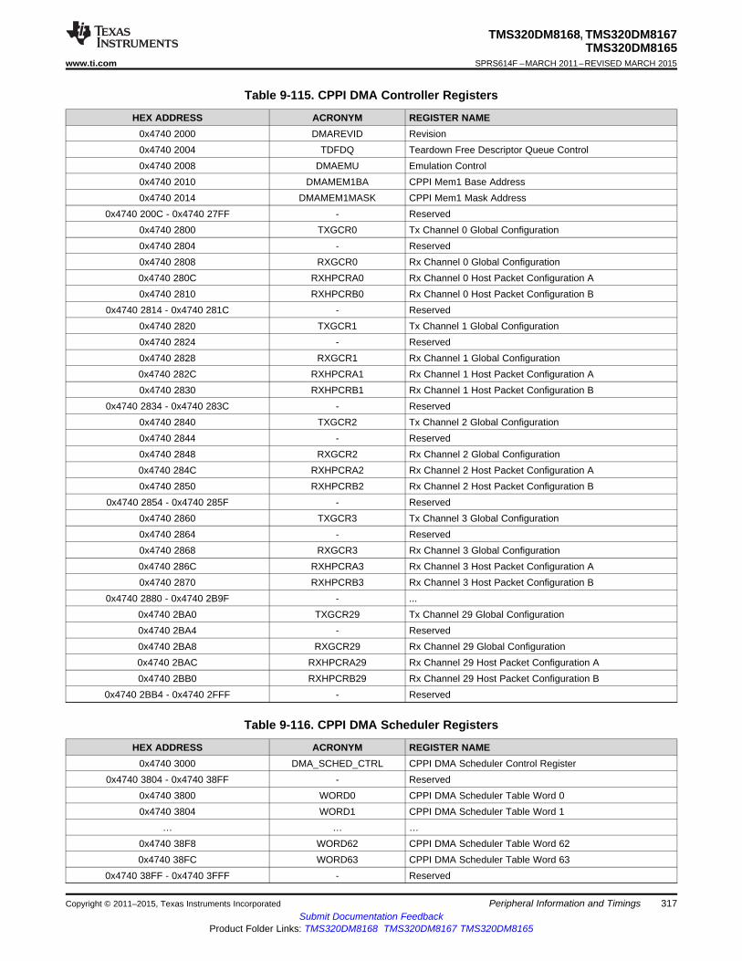
TMS320DM8168, TMS320DM8167TMS320DM8165
www.ti.com SPRS614F –MARCH 2011–REVISED MARCH 2015
Table 9-115. CPPI DMA Controller Registers
HEX ADDRESS ACRONYM REGISTER NAME0x4740 2000 DMAREVID Revision0x4740 2004 TDFDQ Teardown Free Descriptor Queue Control0x4740 2008 DMAEMU Emulation Control0x4740 2010 DMAMEM1BA CPPI Mem1 Base Address0x4740 2014 DMAMEM1MASK CPPI Mem1 Mask Address
0x4740 200C - 0x4740 27FF - Reserved0x4740 2800 TXGCR0 Tx Channel 0 Global Configuration0x4740 2804 - Reserved0x4740 2808 RXGCR0 Rx Channel 0 Global Configuration0x4740 280C RXHPCRA0 Rx Channel 0 Host Packet Configuration A0x4740 2810 RXHPCRB0 Rx Channel 0 Host Packet Configuration B
0x4740 2814 - 0x4740 281C - Reserved0x4740 2820 TXGCR1 Tx Channel 1 Global Configuration0x4740 2824 - Reserved0x4740 2828 RXGCR1 Rx Channel 1 Global Configuration0x4740 282C RXHPCRA1 Rx Channel 1 Host Packet Configuration A0x4740 2830 RXHPCRB1 Rx Channel 1 Host Packet Configuration B
0x4740 2834 - 0x4740 283C - Reserved0x4740 2840 TXGCR2 Tx Channel 2 Global Configuration0x4740 2844 - Reserved0x4740 2848 RXGCR2 Rx Channel 2 Global Configuration0x4740 284C RXHPCRA2 Rx Channel 2 Host Packet Configuration A0x4740 2850 RXHPCRB2 Rx Channel 2 Host Packet Configuration B
0x4740 2854 - 0x4740 285F - Reserved0x4740 2860 TXGCR3 Tx Channel 3 Global Configuration0x4740 2864 - Reserved0x4740 2868 RXGCR3 Rx Channel 3 Global Configuration0x4740 286C RXHPCRA3 Rx Channel 3 Host Packet Configuration A0x4740 2870 RXHPCRB3 Rx Channel 3 Host Packet Configuration B
0x4740 2880 - 0x4740 2B9F - ...0x4740 2BA0 TXGCR29 Tx Channel 29 Global Configuration0x4740 2BA4 - Reserved0x4740 2BA8 RXGCR29 Rx Channel 29 Global Configuration0x4740 2BAC RXHPCRA29 Rx Channel 29 Host Packet Configuration A0x4740 2BB0 RXHPCRB29 Rx Channel 29 Host Packet Configuration B
0x4740 2BB4 - 0x4740 2FFF - Reserved
Table 9-116. CPPI DMA Scheduler Registers
HEX ADDRESS ACRONYM REGISTER NAME0x4740 3000 DMA_SCHED_CTRL CPPI DMA Scheduler Control Register
0x4740 3804 - 0x4740 38FF - Reserved0x4740 3800 WORD0 CPPI DMA Scheduler Table Word 00x4740 3804 WORD1 CPPI DMA Scheduler Table Word 1
… … …0x4740 38F8 WORD62 CPPI DMA Scheduler Table Word 620x4740 38FC WORD63 CPPI DMA Scheduler Table Word 63
0x4740 38FF - 0x4740 3FFF - Reserved
Copyright © 2011–2015, Texas Instruments Incorporated Peripheral Information and Timings 317Submit Documentation Feedback
Product Folder Links: TMS320DM8168 TMS320DM8167 TMS320DM8165
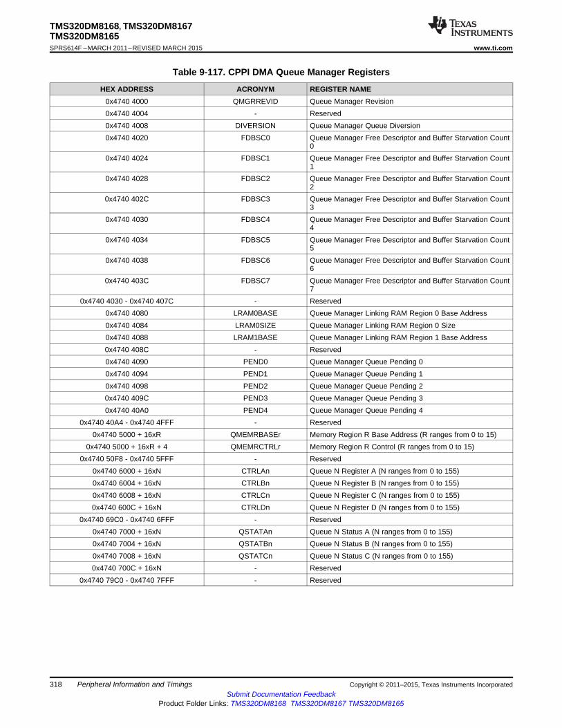
TMS320DM8168, TMS320DM8167TMS320DM8165SPRS614F –MARCH 2011–REVISED MARCH 2015 www.ti.com
Table 9-117. CPPI DMA Queue Manager Registers
HEX ADDRESS ACRONYM REGISTER NAME0x4740 4000 QMGRREVID Queue Manager Revision0x4740 4004 - Reserved0x4740 4008 DIVERSION Queue Manager Queue Diversion0x4740 4020 FDBSC0 Queue Manager Free Descriptor and Buffer Starvation Count
00x4740 4024 FDBSC1 Queue Manager Free Descriptor and Buffer Starvation Count
10x4740 4028 FDBSC2 Queue Manager Free Descriptor and Buffer Starvation Count
20x4740 402C FDBSC3 Queue Manager Free Descriptor and Buffer Starvation Count
30x4740 4030 FDBSC4 Queue Manager Free Descriptor and Buffer Starvation Count
40x4740 4034 FDBSC5 Queue Manager Free Descriptor and Buffer Starvation Count
50x4740 4038 FDBSC6 Queue Manager Free Descriptor and Buffer Starvation Count
60x4740 403C FDBSC7 Queue Manager Free Descriptor and Buffer Starvation Count
70x4740 4030 - 0x4740 407C - Reserved
0x4740 4080 LRAM0BASE Queue Manager Linking RAM Region 0 Base Address0x4740 4084 LRAM0SIZE Queue Manager Linking RAM Region 0 Size0x4740 4088 LRAM1BASE Queue Manager Linking RAM Region 1 Base Address0x4740 408C - Reserved0x4740 4090 PEND0 Queue Manager Queue Pending 00x4740 4094 PEND1 Queue Manager Queue Pending 10x4740 4098 PEND2 Queue Manager Queue Pending 20x4740 409C PEND3 Queue Manager Queue Pending 30x4740 40A0 PEND4 Queue Manager Queue Pending 4
0x4740 40A4 - 0x4740 4FFF - Reserved0x4740 5000 + 16xR QMEMRBASEr Memory Region R Base Address (R ranges from 0 to 15)
0x4740 5000 + 16xR + 4 QMEMRCTRLr Memory Region R Control (R ranges from 0 to 15)0x4740 50F8 - 0x4740 5FFF - Reserved
0x4740 6000 + 16xN CTRLAn Queue N Register A (N ranges from 0 to 155)0x4740 6004 + 16xN CTRLBn Queue N Register B (N ranges from 0 to 155)0x4740 6008 + 16xN CTRLCn Queue N Register C (N ranges from 0 to 155)0x4740 600C + 16xN CTRLDn Queue N Register D (N ranges from 0 to 155)
0x4740 69C0 - 0x4740 6FFF - Reserved0x4740 7000 + 16xN QSTATAn Queue N Status A (N ranges from 0 to 155)0x4740 7004 + 16xN QSTATBn Queue N Status B (N ranges from 0 to 155)0x4740 7008 + 16xN QSTATCn Queue N Status C (N ranges from 0 to 155)0x4740 700C + 16xN - Reserved
0x4740 79C0 - 0x4740 7FFF - Reserved
318 Peripheral Information and Timings Copyright © 2011–2015, Texas Instruments IncorporatedSubmit Documentation Feedback
Product Folder Links: TMS320DM8168 TMS320DM8167 TMS320DM8165

USB_VSSREF USB_R1
USB
44.2- ±1%Ω(A)
trtf
VCRS90% VOH
10% VOL
USB_DN
USB_DP
tper − tjr
TMS320DM8168, TMS320DM8167TMS320DM8165
www.ti.com SPRS614F –MARCH 2011–REVISED MARCH 2015
9.21.2 USB2.0 Electrical Data and Timing
Table 9-118. Switching Characteristics Over Recommended Operating Conditions for USB2.0(see Figure 9-90)
LOW SPEED FULL SPEED HIGH SPEED1.5 Mbps 12 Mbps 480 MbpsNO. PARAMETER UNITMIN MAX MIN MAX MIN MAX
1 tr(D) Rise time, USB_DP and USB_DN signals (1) 75 300 4 20 0.5 ns2 tf(D) Fall time, USB_DP and USB_DN signals (1) 75 300 4 20 0.5 ns3 trfM Rise and Fall time, matching (2) 80 125 90 111.11 – – %4 VCRS Output signal cross-over voltage (1) 1.3 2 1.3 2 – – V5 tjr(source)NT Source (Host) Driver jitter, next transition 2 2 (3) ns
tjr(FUNC)NT Function Driver jitter, next transition 25 2 (3) ns6 tjr(source)PT Source (Host) Driver jitter, paired transition (4) 1 1 (3) ns
tjr(FUNC)PT Function Driver jitter, paired transition 10 1 (3) ns7 tw(EOPT) Pulse duration, EOP transmitter 1250 1500 160 175 – – ns8 tw(EOPR) Pulse duration, EOP receiver 670 82 – ns
Mb9 t(DRATE) Data Rate 1.5 12 480 per s10 ZDRV Driver Output Resistance – – 28 49.5 40.5 49.5 Ω11 USB_R1 USB reference resistor 43.8 44.6 43.8 44.6 43.8 44.6 Ω
(1) Low Speed: CL = 200 pF, Full Speed: CL = 50 pF, High Speed: CL = 50 pF(2) tRFM = (tr/tf) x 100. [Excluding the first transaction from the Idle state.](3) For more detailed information, see the Universal Serial Bus Specification Revision 2.0, Chapter 7, Electrical.(4) tjr = tpx(1) - tpx(0)
Figure 9-90. USB2.0 Integrated Transceiver Interface Timing
A. Place the 44.2-Ω ± 1% as close to the device as possible.
Figure 9-91. USB Reference Resistor Routing
Copyright © 2011–2015, Texas Instruments Incorporated Peripheral Information and Timings 319Submit Documentation Feedback
Product Folder Links: TMS320DM8168 TMS320DM8167 TMS320DM8165

TMS320DM8168, TMS320DM8167TMS320DM8165SPRS614F –MARCH 2011–REVISED MARCH 2015 www.ti.com
10 Device and Documentation Support
10.1 Device Support
10.1.1 Development SupportTI offers an extensive line of development tools, including tools to evaluate the performance of theprocessors, generate code, develop algorithm implementations, and fully integrate and debug softwareand hardware modules. The tool's support documentation is electronically available within the CodeComposer Studio™ Integrated Development Environment (IDE).
The following products support development of TMS320DM816x processor applications:
Software Development Tools: Code Composer Studio™ Integrated Development Environment (IDE):including Editor C/C++ and Assembly Code Generation, and Debug plus additional development toolsScalable, Real-Time Foundation Software DSP/BIOS™, which provides the basic run-time target softwareneeded to support any DaVinci Video Processor application.
Hardware Development Tools: Extended Development System ( XDS™) Emulator
For a complete listing of development-support tools for the DM816x DaVinci™ Video Processor platform,visit the Texas Instruments website at www.ti.com. For information on pricing and availability, contact thenearest TI field sales office or authorized distributor.
Device and Development Support-Tool NomenclatureTo designate the stages in the product development cycle, TI assigns prefixes to the part numbers of allDSP devices and support tools. Each DSP commercial family member has one of three prefixes: TMX,TMP, or TMS (for example, TMS320DM8168CYG). Texas Instruments recommends two of three possibleprefix designators for its support tools: TMDX and TMDS. These prefixes represent evolutionary stages ofproduct development from engineering prototypes (TMX and TMDX) through fully qualified productiondevices and tools (TMS and TMDS).
Device development evolutionary flow:
TMX Experimental device that is not necessarily representative of the final device's electricalspecifications and may not use production assembly flow.
TMP Prototype device that is not necessarily the final silicon die and may not necessarily meetfinal electrical specifications.
TMS Production version of the silicon die that is fully qualified.
Support tool development evolutionary flow:
TMDX Development-support product that has not yet completed Texas Instruments internalqualification testing.
TMDS Fully-qualified development-support product.
TMX and TMP devices and TMDX development-support tools are shipped against the followingdisclaimer:
"Developmental product is intended for internal evaluation purposes."
Production devices and TMDS development-support tools have been characterized fully, and the qualityand reliability of the device have been demonstrated fully. TI's standard warranty applies.
Predictions show that prototype devices (TMX or TMP) have a greater failure rate than the standardproduction devices. Texas Instruments recommends that these devices not be used in any productionsystem because their expected end-use failure rate still is undefined. Only qualified production devices areto be used.
320 Device and Documentation Support Copyright © 2011–2015, Texas Instruments IncorporatedSubmit Documentation Feedback
Product Folder Links: TMS320DM8168 TMS320DM8167 TMS320DM8165
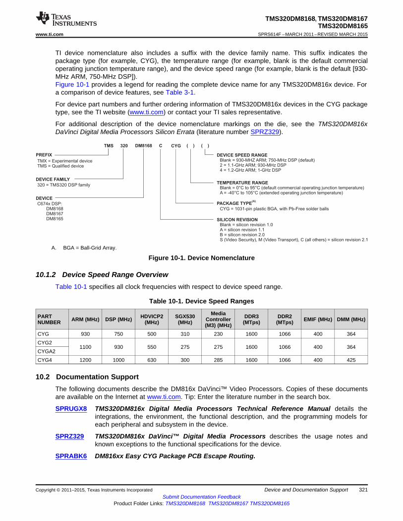
PREFIX
TMS 320 DM8168
TMX = Experimental deviceTMS = Qualified device
DEVICE FAMILY
320 = TMS320 DSP family
C674x DSP:DM8168DM8167DM8165
DEVICE
CYG
PACKAGE TYPE(A)
CYG = 1031-pin plastic BGA, with Pb-Free solder balls
DEVICE SPEED RANGEBlank = 930-MHZ ARM; 750-MHz DSP (default)2 = 1.1-GHz ARM; 930-MHz DSP4 = 1.2-GHz ARM; 1-GHz DSP
( )
TEMPERATURE RANGEBlank = 0°C to 95°C (default commercial operating junction temperature)A = -40°C to 105°C (extended operating junction temperature)
( )C
SILICON REVISIONBlank = silicon revision 1.0A = silicon revision 1.1B = silicon revision 2.0S (Video Security), M (Video Transport), C (all others) = silicon revision 2.1
TMS320DM8168, TMS320DM8167TMS320DM8165
www.ti.com SPRS614F –MARCH 2011–REVISED MARCH 2015
TI device nomenclature also includes a suffix with the device family name. This suffix indicates thepackage type (for example, CYG), the temperature range (for example, blank is the default commercialoperating junction temperature range), and the device speed range (for example, blank is the default [930-MHz ARM, 750-MHz DSP]).Figure 10-1 provides a legend for reading the complete device name for any TMS320DM816x device. Fora comparison of device features, see Table 3-1.
For device part numbers and further ordering information of TMS320DM816x devices in the CYG packagetype, see the TI website (www.ti.com) or contact your TI sales representative.
For additional description of the device nomenclature markings on the die, see the TMS320DM816xDaVinci Digital Media Processors Silicon Errata (literature number SPRZ329).
A. BGA = Ball-Grid Array.
Figure 10-1. Device Nomenclature
10.1.2 Device Speed Range OverviewTable 10-1 specifies all clock frequencies with respect to device speed range.
Table 10-1. Device Speed Ranges
MediaPART HDVICP2 SGX530 DDR3 DDR2ARM (MHz) DSP (MHz) Controller EMIF (MHz) DMM (MHz)NUMBER (MHz) (MHz) (MTps) (MTps)(M3) (MHz)CYG 930 750 500 310 230 1600 1066 400 364CYG2
1100 930 550 275 275 1600 1066 400 364CYGA2CYG4 1200 1000 630 300 285 1600 1066 400 425
10.2 Documentation SupportThe following documents describe the DM816x DaVinci™ Video Processors. Copies of these documentsare available on the Internet at www.ti.com. Tip: Enter the literature number in the search box.
SPRUGX8 TMS320DM816x Digital Media Processors Technical Reference Manual details theintegrations, the environment, the functional description, and the programming models foreach peripheral and subsystem in the device.
SPRZ329 TMS320DM816x DaVinci™ Digital Media Processors describes the usage notes andknown exceptions to the functional specifications for the device.
SPRABK6 DM816xx Easy CYG Package PCB Escape Routing.
Copyright © 2011–2015, Texas Instruments Incorporated Device and Documentation Support 321Submit Documentation Feedback
Product Folder Links: TMS320DM8168 TMS320DM8167 TMS320DM8165

TMS320DM8168, TMS320DM8167TMS320DM8165SPRS614F –MARCH 2011–REVISED MARCH 2015 www.ti.com
10.3 Related LinksThe table below lists quick access links. Categories include technical documents, support and communityresources, tools and software, and quick access to sample or buy.
Table 10-2. Related Links
TECHNICAL TOOLS & SUPPORT &PARTS PRODUCT FOLDER SAMPLE & BUY DOCUMENTS SOFTWARE COMMUNITYTMS320DM8168 Click here Click here Click here Click here Click hereTMS320DM8167 Click here Click here Click here Click here Click hereTMS320DM8165 Click here Click here Click here Click here Click here
10.4 Community ResourcesThe following links connect to TI community resources. Linked contents are provided "AS IS" by therespective contributors. They do not constitute TI specifications and do not necessarily reflect TI's views;see TI's Terms of Use.
TI E2E™ Online Community TI's Engineer-to-Engineer (E2E) Community. Created to fostercollaboration among engineers. At e2e.ti.com, you can ask questions, share knowledge,explore ideas and help solve problems with fellow engineers.
TI Embedded Processors Wiki Texas Instruments Embedded Processors Wiki. Established to helpdevelopers get started with Embedded Processors from Texas Instruments and to fosterinnovation and growth of general knowledge about the hardware and software surroundingthese devices.
10.5 TrademarksDaVinci, C674x, C64x+, SmartReflex, TMS320C6000, Code Composer Studio, DSP/BIOS, XDS, E2E aretrademarks of Texas Instruments.Cortex, NEON are trademarks of ARM Limited.Jazelle is a registered trademark of ARM Limited.Thumb is a registered trademark of ARM Ltd or its subsidiaries.USSE is a trademark of Imagination Technologies Limited.PowerVR is a registered trademark of Imagination Technologies Limited.OpenVG, OpenMax are trademarks of Khronos, Group Inc..OpenGL is a registered trademark of Khronos, Group Inc..Microsoft, Windows are registered trademarks of Microsoft Corp.Direct3D is a registered trademark of Microsoft.I2C bus is a registered trademark of NXP B.V. Corporation Netherlands.PCI Express is a registered trademark of PCI-SIG.Via Channel is a trademark of Via Technologies, Inc..
10.6 Electrostatic Discharge CautionThis integrated circuit can be damaged by ESD. Texas Instruments recommends that all integrated circuits be handled withappropriate precautions. Failure to observe proper handling and installation procedures can cause damage.
ESD damage can range from subtle performance degradation to complete device failure. Precision integrated circuits may be moresusceptible to damage because very small parametric changes could cause the device not to meet its published specifications.
10.7 GlossarySLYZ022 — TI Glossary.
This glossary lists and explains terms, acronyms, and definitions.
322 Device and Documentation Support Copyright © 2011–2015, Texas Instruments IncorporatedSubmit Documentation Feedback
Product Folder Links: TMS320DM8168 TMS320DM8167 TMS320DM8165
TMS320DM8168, TMS320DM8167TMS320DM8165
www.ti.com SPRS614F –MARCH 2011–REVISED MARCH 2015
11 Mechanical Packaging and Orderable Information
11.1 Packaging InformationThe following pages include mechanical packaging and orderable information. This information is the mostcurrent data available for the designated devices. This data is subject to change without notice andrevision of this document. For browser-based versions of this data sheet, refer to the left-hand navigation.
Copyright © 2011–2015, Texas Instruments Incorporated Mechanical Packaging and Orderable Information 323Submit Documentation Feedback
Product Folder Links: TMS320DM8168 TMS320DM8167 TMS320DM8165

PACKAGE OPTION ADDENDUM
www.ti.com 24-Aug-2018
Addendum-Page 1
PACKAGING INFORMATION
Orderable Device Status(1)
Package Type PackageDrawing
Pins PackageQty
Eco Plan(2)
Lead/Ball Finish(6)
MSL Peak Temp(3)
Op Temp (°C) Device Marking(4/5)
Samples
TMS320DM8165SCYG ACTIVE FCBGA CYG 1031 44 Green (RoHS& no Sb/Br)
SNAGCU Level-4-245C-72HR 0 to 95 TMS320DM8165SCYG
TMS320DM8165SCYG2 ACTIVE FCBGA CYG 1031 44 Green (RoHS& no Sb/Br)
SNAGCU Level-4-245C-72HR 0 to 95 TMS320DM8165SCYG2
TMS320DM8165SCYG4 ACTIVE FCBGA CYG 1031 44 Green (RoHS& no Sb/Br)
SNAGCU Level-4-245C-72HR 0 to 95 TMS320DM8165SCYG4
TMS320DM8167SCYG ACTIVE FCBGA CYG 1031 44 Green (RoHS& no Sb/Br)
SNAGCU Level-4-245C-72HR 0 to 95 TMS320DM8167SCYG
TMS320DM8167SCYG2 ACTIVE FCBGA CYG 1031 44 Green (RoHS& no Sb/Br)
SNAGCU Level-4-245C-72HR 0 to 95 TMS320DM8167SCYG2
TMS320DM8167SCYG4 ACTIVE FCBGA CYG 1031 44 Green (RoHS& no Sb/Br)
SNAGCU Level-4-245C-72HR 0 to 95 TMS320DM8167SCYG4
TMS320DM8168CCYG ACTIVE FCBGA CYG 1031 44 Green (RoHS& no Sb/Br)
SNAGCU Level-4-245C-72HR 0 to 95 TMS320DM8168CCYG
TMS320DM8168CCYG2 ACTIVE FCBGA CYG 1031 44 Green (RoHS& no Sb/Br)
SNAGCU Level-4-245C-72HR 0 to 95 TMS320DM8168CCYG2
TMS320DM8168CCYG4 ACTIVE FCBGA CYG 1031 44 Green (RoHS& no Sb/Br)
SNAGCU Level-4-245C-72HR 0 to 95 TMS320DM8168CCYG4
TMS320DM8168CCYGA2 ACTIVE FCBGA CYG 1031 44 Green (RoHS& no Sb/Br)
SNAGCU Level-4-245C-72HR -40 to 105 TMS320DM8168CCYGA2
TMS320DM8168CCYGH ACTIVE FCBGA CYG 1031 44 Green (RoHS& no Sb/Br)
SNAGCU Level-4-245C-72HR 0 to 95 TMS320DM8168CCYGH
TMS320DM8168SCYG ACTIVE FCBGA CYG 1031 44 Green (RoHS& no Sb/Br)
SNAGCU Level-4-245C-72HR 0 to 95 TMS320DM8168SCYG
TMS320DM8168SCYG2 ACTIVE FCBGA CYG 1031 44 Green (RoHS& no Sb/Br)
SNAGCU Level-4-245C-72HR 0 to 95 TMS320DM8168SCYG2

PACKAGE OPTION ADDENDUM
www.ti.com 24-Aug-2018
Addendum-Page 2
Orderable Device Status(1)
Package Type PackageDrawing
Pins PackageQty
Eco Plan(2)
Lead/Ball Finish(6)
MSL Peak Temp(3)
Op Temp (°C) Device Marking(4/5)
Samples
TMS320DM8168SCYG4 ACTIVE FCBGA CYG 1031 44 Green (RoHS& no Sb/Br)
SNAGCU Level-4-245C-72HR 0 to 95 TMS320DM8168SCYG4
TMS320DM8168SCYGA2 ACTIVE FCBGA CYG 1031 44 Green (RoHS& no Sb/Br)
SNAGCU Level-4-245C-72HR -40 to 105 TMS320DM8168SCYGA2
(1) The marketing status values are defined as follows:ACTIVE: Product device recommended for new designs.LIFEBUY: TI has announced that the device will be discontinued, and a lifetime-buy period is in effect.NRND: Not recommended for new designs. Device is in production to support existing customers, but TI does not recommend using this part in a new design.PREVIEW: Device has been announced but is not in production. Samples may or may not be available.OBSOLETE: TI has discontinued the production of the device.
(2) RoHS: TI defines "RoHS" to mean semiconductor products that are compliant with the current EU RoHS requirements for all 10 RoHS substances, including the requirement that RoHS substancedo not exceed 0.1% by weight in homogeneous materials. Where designed to be soldered at high temperatures, "RoHS" products are suitable for use in specified lead-free processes. TI mayreference these types of products as "Pb-Free".RoHS Exempt: TI defines "RoHS Exempt" to mean products that contain lead but are compliant with EU RoHS pursuant to a specific EU RoHS exemption.Green: TI defines "Green" to mean the content of Chlorine (Cl) and Bromine (Br) based flame retardants meet JS709B low halogen requirements of <=1000ppm threshold. Antimony trioxide basedflame retardants must also meet the <=1000ppm threshold requirement.
(3) MSL, Peak Temp. - The Moisture Sensitivity Level rating according to the JEDEC industry standard classifications, and peak solder temperature.
(4) There may be additional marking, which relates to the logo, the lot trace code information, or the environmental category on the device.
(5) Multiple Device Markings will be inside parentheses. Only one Device Marking contained in parentheses and separated by a "~" will appear on a device. If a line is indented then it is a continuationof the previous line and the two combined represent the entire Device Marking for that device.
(6) Lead/Ball Finish - Orderable Devices may have multiple material finish options. Finish options are separated by a vertical ruled line. Lead/Ball Finish values may wrap to two lines if the finishvalue exceeds the maximum column width.
Important Information and Disclaimer:The information provided on this page represents TI's knowledge and belief as of the date that it is provided. TI bases its knowledge and belief on informationprovided by third parties, and makes no representation or warranty as to the accuracy of such information. Efforts are underway to better integrate information from third parties. TI has taken andcontinues to take reasonable steps to provide representative and accurate information but may not have conducted destructive testing or chemical analysis on incoming materials and chemicals.TI and TI suppliers consider certain information to be proprietary, and thus CAS numbers and other limited information may not be available for release.
In no event shall TI's liability arising out of such information exceed the total purchase price of the TI part(s) at issue in this document sold by TI to Customer on an annual basis.

IMPORTANT NOTICE
Texas Instruments Incorporated (TI) reserves the right to make corrections, enhancements, improvements and other changes to itssemiconductor products and services per JESD46, latest issue, and to discontinue any product or service per JESD48, latest issue. Buyersshould obtain the latest relevant information before placing orders and should verify that such information is current and complete.TI’s published terms of sale for semiconductor products (http://www.ti.com/sc/docs/stdterms.htm) apply to the sale of packaged integratedcircuit products that TI has qualified and released to market. Additional terms may apply to the use or sale of other types of TI products andservices.Reproduction of significant portions of TI information in TI data sheets is permissible only if reproduction is without alteration and isaccompanied by all associated warranties, conditions, limitations, and notices. TI is not responsible or liable for such reproduceddocumentation. Information of third parties may be subject to additional restrictions. Resale of TI products or services with statementsdifferent from or beyond the parameters stated by TI for that product or service voids all express and any implied warranties for theassociated TI product or service and is an unfair and deceptive business practice. TI is not responsible or liable for any such statements.Buyers and others who are developing systems that incorporate TI products (collectively, “Designers”) understand and agree that Designersremain responsible for using their independent analysis, evaluation and judgment in designing their applications and that Designers havefull and exclusive responsibility to assure the safety of Designers' applications and compliance of their applications (and of all TI productsused in or for Designers’ applications) with all applicable regulations, laws and other applicable requirements. Designer represents that, withrespect to their applications, Designer has all the necessary expertise to create and implement safeguards that (1) anticipate dangerousconsequences of failures, (2) monitor failures and their consequences, and (3) lessen the likelihood of failures that might cause harm andtake appropriate actions. Designer agrees that prior to using or distributing any applications that include TI products, Designer willthoroughly test such applications and the functionality of such TI products as used in such applications.TI’s provision of technical, application or other design advice, quality characterization, reliability data or other services or information,including, but not limited to, reference designs and materials relating to evaluation modules, (collectively, “TI Resources”) are intended toassist designers who are developing applications that incorporate TI products; by downloading, accessing or using TI Resources in anyway, Designer (individually or, if Designer is acting on behalf of a company, Designer’s company) agrees to use any particular TI Resourcesolely for this purpose and subject to the terms of this Notice.TI’s provision of TI Resources does not expand or otherwise alter TI’s applicable published warranties or warranty disclaimers for TIproducts, and no additional obligations or liabilities arise from TI providing such TI Resources. TI reserves the right to make corrections,enhancements, improvements and other changes to its TI Resources. TI has not conducted any testing other than that specificallydescribed in the published documentation for a particular TI Resource.Designer is authorized to use, copy and modify any individual TI Resource only in connection with the development of applications thatinclude the TI product(s) identified in such TI Resource. NO OTHER LICENSE, EXPRESS OR IMPLIED, BY ESTOPPEL OR OTHERWISETO ANY OTHER TI INTELLECTUAL PROPERTY RIGHT, AND NO LICENSE TO ANY TECHNOLOGY OR INTELLECTUAL PROPERTYRIGHT OF TI OR ANY THIRD PARTY IS GRANTED HEREIN, including but not limited to any patent right, copyright, mask work right, orother intellectual property right relating to any combination, machine, or process in which TI products or services are used. Informationregarding or referencing third-party products or services does not constitute a license to use such products or services, or a warranty orendorsement thereof. Use of TI Resources may require a license from a third party under the patents or other intellectual property of thethird party, or a license from TI under the patents or other intellectual property of TI.TI RESOURCES ARE PROVIDED “AS IS” AND WITH ALL FAULTS. TI DISCLAIMS ALL OTHER WARRANTIES ORREPRESENTATIONS, EXPRESS OR IMPLIED, REGARDING RESOURCES OR USE THEREOF, INCLUDING BUT NOT LIMITED TOACCURACY OR COMPLETENESS, TITLE, ANY EPIDEMIC FAILURE WARRANTY AND ANY IMPLIED WARRANTIES OFMERCHANTABILITY, FITNESS FOR A PARTICULAR PURPOSE, AND NON-INFRINGEMENT OF ANY THIRD PARTY INTELLECTUALPROPERTY RIGHTS. TI SHALL NOT BE LIABLE FOR AND SHALL NOT DEFEND OR INDEMNIFY DESIGNER AGAINST ANY CLAIM,INCLUDING BUT NOT LIMITED TO ANY INFRINGEMENT CLAIM THAT RELATES TO OR IS BASED ON ANY COMBINATION OFPRODUCTS EVEN IF DESCRIBED IN TI RESOURCES OR OTHERWISE. IN NO EVENT SHALL TI BE LIABLE FOR ANY ACTUAL,DIRECT, SPECIAL, COLLATERAL, INDIRECT, PUNITIVE, INCIDENTAL, CONSEQUENTIAL OR EXEMPLARY DAMAGES INCONNECTION WITH OR ARISING OUT OF TI RESOURCES OR USE THEREOF, AND REGARDLESS OF WHETHER TI HAS BEENADVISED OF THE POSSIBILITY OF SUCH DAMAGES.Unless TI has explicitly designated an individual product as meeting the requirements of a particular industry standard (e.g., ISO/TS 16949and ISO 26262), TI is not responsible for any failure to meet such industry standard requirements.Where TI specifically promotes products as facilitating functional safety or as compliant with industry functional safety standards, suchproducts are intended to help enable customers to design and create their own applications that meet applicable functional safety standardsand requirements. Using products in an application does not by itself establish any safety features in the application. Designers mustensure compliance with safety-related requirements and standards applicable to their applications. Designer may not use any TI products inlife-critical medical equipment unless authorized officers of the parties have executed a special contract specifically governing such use.Life-critical medical equipment is medical equipment where failure of such equipment would cause serious bodily injury or death (e.g., lifesupport, pacemakers, defibrillators, heart pumps, neurostimulators, and implantables). Such equipment includes, without limitation, allmedical devices identified by the U.S. Food and Drug Administration as Class III devices and equivalent classifications outside the U.S.TI may expressly designate certain products as completing a particular qualification (e.g., Q100, Military Grade, or Enhanced Product).Designers agree that it has the necessary expertise to select the product with the appropriate qualification designation for their applicationsand that proper product selection is at Designers’ own risk. Designers are solely responsible for compliance with all legal and regulatoryrequirements in connection with such selection.Designer will fully indemnify TI and its representatives against any damages, costs, losses, and/or liabilities arising out of Designer’s non-compliance with the terms and provisions of this Notice.
Mailing Address: Texas Instruments, Post Office Box 655303, Dallas, Texas 75265Copyright © 2018, Texas Instruments Incorporated
Related Documents


