Design and Implementation of High Speed Serial Pheripheral Interface (SPI) and Static Verification using Linting tool Under the Guidance of Prof . SUJATHA HIREMATH VIJETH S ANCHATGERI 1RV13LVS32

Welcome message from author
This document is posted to help you gain knowledge. Please leave a comment to let me know what you think about it! Share it to your friends and learn new things together.
Transcript

Design and Implementation of High Speed Serial Pheripheral Interface (SPI) and Static Verification using Linting tool
Under the Guidance of
Prof . SUJATHA HIREMATH
VIJETH S ANCHATGERI
1RV13LVS32

OVER-VIEW
• SPI• Motivation• Bock diagram• Master and Slave Core• SPI Protocol• Sub blocks• Static Verification
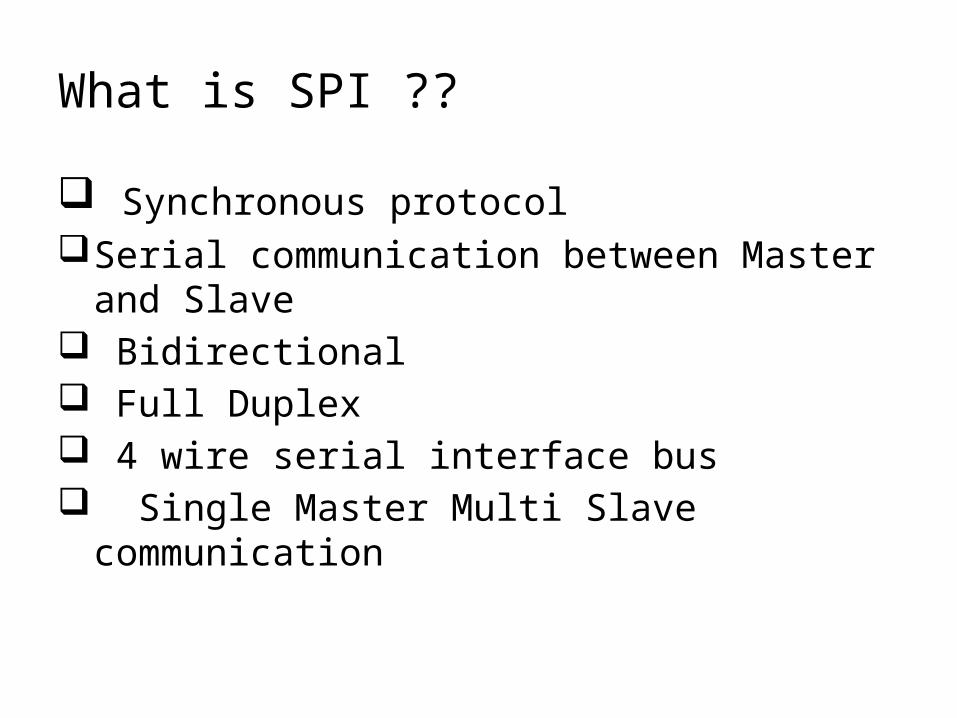
What is SPI ??
Synchronous protocol Serial communication between Master and Slave Bidirectional Full Duplex 4 wire serial interface bus Single Master Multi Slave communication

MotivationWhy SPI ??
When a communication is needed between microcontroller and set of slow peripherals there is no point in use of complex protocols, SPI suits the best
Best suited for communications between integrated circuits with on-board peripherals
Supports both inter-chip and intra-chip with low and medium Bandwidth data transfer
High speed data transferSimple architecture Less no of pins

SPI Block diagram

SPI Master Core

SPI SLAVE CORE

SPI Protocol
The SPI uses 4 logic signals for Transmission across its Interface
SCLK - SERIAL CLOCK (Output from Master) MOSI- MASTER OUTPUT SLAVE INPUT MISO-MASTER INPUT SLAVE OUTPUT SS-SLAVE SELECT (CHIP SELECT)
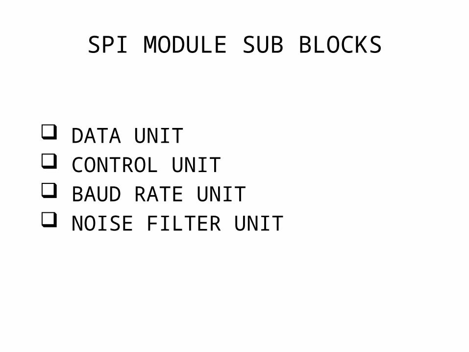
SPI MODULE SUB BLOCKS
DATA UNIT CONTROL UNIT BAUD RATE UNIT NOISE FILTER UNIT
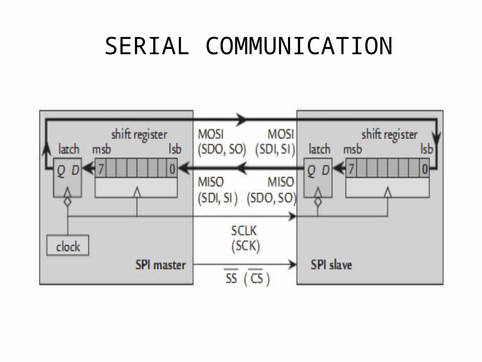
SERIAL COMMUNICATION

STATIC VERIFICATION

LINT RULE CHECK
• LINT: program that flagged suspicious and non-portable constructs in RTL Design
• check the cleanness and portability of the HDLs code for various EDA tools.
• RULE CHECK: A set of rules are defined in the lint tool. Rule means a condition that has to be checked on your design

Various Rule Checks
• Unintended latches or combo loops• Clocks and reset definitions.• Connectivity checks for clocks, resets, and tri-state
driven signals• FSM state reachability and coding issues• Chances of matching gate level simulations with RTL
simulations• Width mismatch in netlist• Clock domain Crossings

Work to be done
• Design of SPI Master core• Design of SPI Slave core• Current design has input arrival time before clock for
master 1.72ns and slave 1.663ns• Improve the speed of operation compared to existing
architecture• Incorporating the flexibility of handling Two slaves
simultaneously at a time with no performance degradation
• Static Verification of RTL Design • Implement the design on FPGA.

References
[1] A.K. Oudjida, M.L. Berrandjia, A. Liacha, R. Tiar, K. Tahraoui & Y.N. Alhoumays, “ Design and Test of General-Purpose SPI Master/Slave IPs on OPB Bus,” 2010 IEEE.
[2] Frederic Leens, “An introduction to SPI and I2C protocol,” IEEE Instrumentation and Measurement magazine, February 2009.
[3] A.K. Oudjida et al, “FPGA Implementation of I2C and SPI Protocols: A Comparative Study,” Proceedings of the 16th edition of the IEEE International Conference on Electronics Circuits and Systems ICECS, pp. 507 -510, December 13-16, 2009.
[4] On-chip communication protocols , system on-chip interconnect, by Sudeep Pasricha and Nikil Dutt,Morgan Kaufmann series 2008.