Spintronics in metals and semiconductors Tomas Jungwirth University of Nottingham Bryan Gallagher, Tom Foxon, Richard Campion, Kevin Edmond Andrew Rushforth, Chris King et Hitachi Cambridge Jorg Wunderlich, Andrew Irvine, David Williams, Elisa de Ranieri, Sam Owen, et al. Institute of Physics ASCR Alexander Shick, Karel Výborný, Jan Zemen, Jan Masek, Vít Novák, Kamil Olejník, et al.

Spintronics in metals and semiconductors Tomas Jungwirth University of Nottingham Bryan Gallagher, Tom Foxon, Richard Campion, Kevin Edmonds, Andrew Rushforth,
Dec 16, 2015
Welcome message from author
This document is posted to help you gain knowledge. Please leave a comment to let me know what you think about it! Share it to your friends and learn new things together.
Transcript
Spintronics in metals and semiconductors
Tomas Jungwirth
University of Nottingham Bryan Gallagher, Tom Foxon,
Richard Campion, Kevin Edmonds, Andrew Rushforth, Chris King et al.
Hitachi Cambridge Jorg Wunderlich, Andrew Irvine, David Williams,
Elisa de Ranieri, Sam Owen, et al.
Institute of Physics ASCR Alexander Shick, Karel Výborný, Jan Zemen, Jan Masek, Vít Novák, Kamil Olejník, et al.
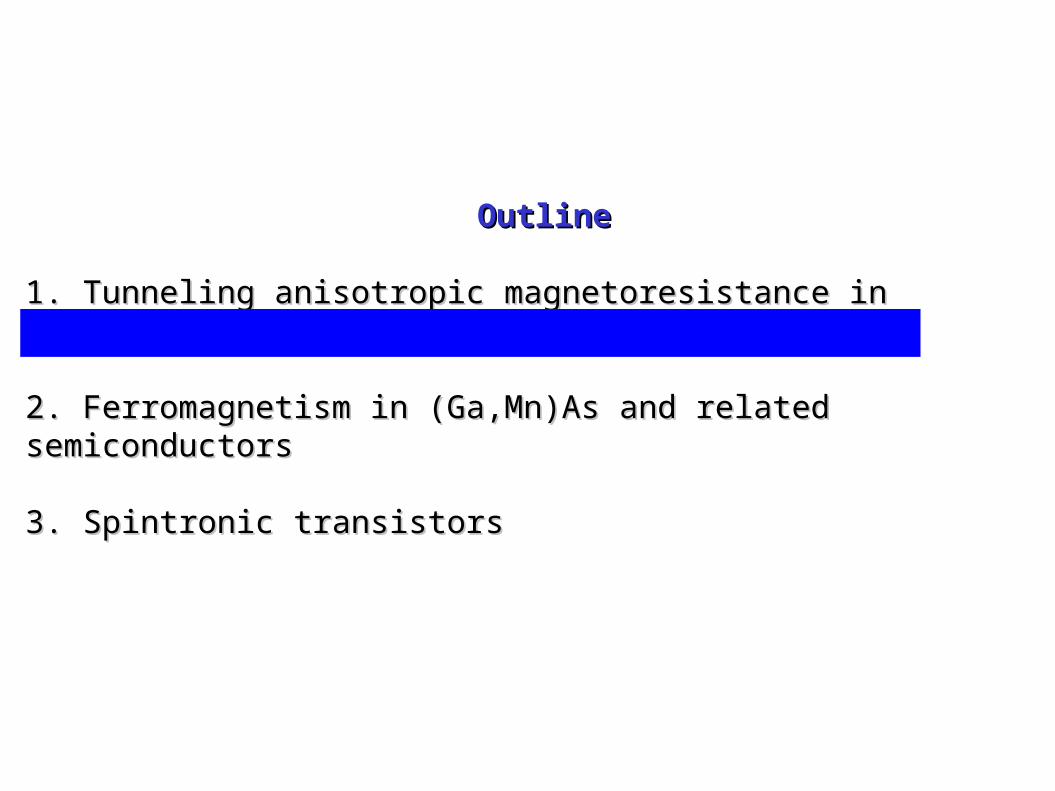
OutlineOutline
11.. Tunneling anisotropic magnetoresistance in transition metals Tunneling anisotropic magnetoresistance in transition metals
2. Ferromagnetism in (Ga,Mn)As and related semiconductors2. Ferromagnetism in (Ga,Mn)As and related semiconductors
3. Spintronic transistors3. Spintronic transistors

Spintronics: Spin-orbit & exchange interactions
nucleus rest frame electron rest frame
vI Q rE3
04 r
Q
3
0
4 r
rIB
EvEvB 200
1
c
EvSS 22
B2 mc
egH B
SO
Thomas precession
Coulomb repulsion & Pauli exclusion principle exchange interaction
ferromagnetism
spin-orbit interaction
DOS

AMRAMR~ 1% MR effect~ 1% MR effect
TMRTMR~ 100% MR effect~ 100% MR effect
TAMRTAMR
) vs.( ~ IMvg
)(BM
M
Exchange int.:
Spin-orbit int.:
magnetic anisotropy
Exchange int.:
)()( TDOSTDOSAFM-FM exchange bias
)(MTDOS
Au

ab intio theory Shick, et al, PRB '06, Park, et al, PRL '08
experiment Park, et al, PRL '08
TAMR in CoPt structures

spontaneous momentmag
netic su
sceptib
ility
Consider uncommon TM combinationsMn/W ~100% TAMR
Consider both Mn-TM FMs & AFMs
exchange-spring rotation of the AFMScholl et al. PRL ‘04
Proposal for AFM-TAMR: first microelectronic device with active AFM component
spin
-orb
it cou
plin
g
TAMR in TM structures
Shick, et al,unpublished
Shick, et al,unpublished
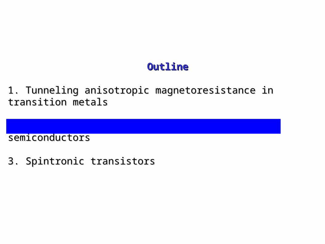
OutlineOutline
11.. Tunneling anisotropic magnetoresistance in transition metals Tunneling anisotropic magnetoresistance in transition metals
2. Ferromagnetism in (Ga,Mn)As and related semiconductors2. Ferromagnetism in (Ga,Mn)As and related semiconductors
3. Spintronic transistors3. Spintronic transistors

Magnetic materials
Ferroelectrics/piezoelectrics Semiconductors
spintronic magneto-sensors, memories
electro-mechanical transducors, large & persistent el. fields
transistors, logic,sensitive to doping and electrical gating
TM-based semiconducting multiferroic spintronicssensors & memories transistors & logic
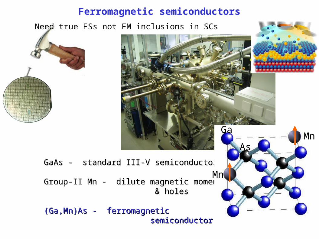
Ferromagnetic semiconductors
GaAs - GaAs - standard III-V semiconductorstandard III-V semiconductor
Group-II Group-II Mn - Mn - dilute dilute magneticmagnetic moments moments & holes& holes
(Ga,Mn)As - fe(Ga,Mn)As - ferrromagneticromagnetic semiconductorsemiconductor
Need true FSs not FM inclusions in SCs
Mn
Ga
AsMn
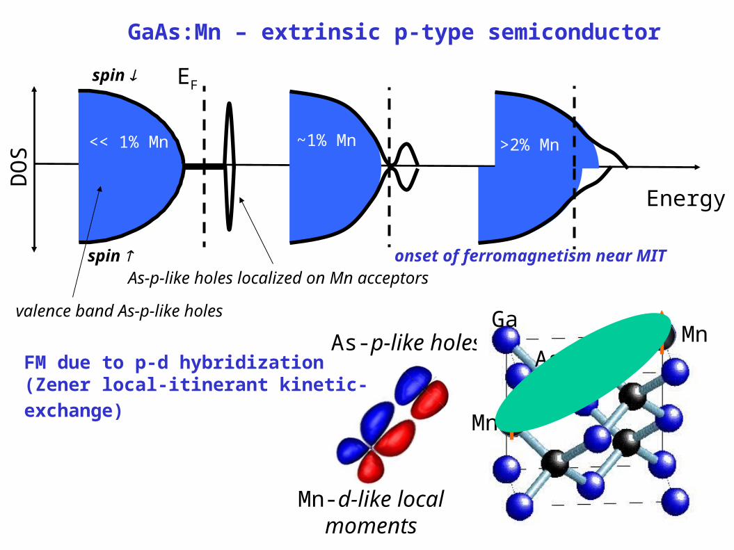
Mn-d-like localmoments
As-p-like holes
Mn
Ga
AsMn
EF
DO
S
Energy
spin
spin
GaAs:Mn – extrinsic p-type semiconductor
FM due to p-d hybridization
(Zener local-itinerant kinetic-exchange)
valence band As-p-like holes
As-p-like holes localized on Mn acceptors
<< 1% Mn ~1% Mn >2% Mn
onset of ferromagnetism near MIT
As-p-like holes
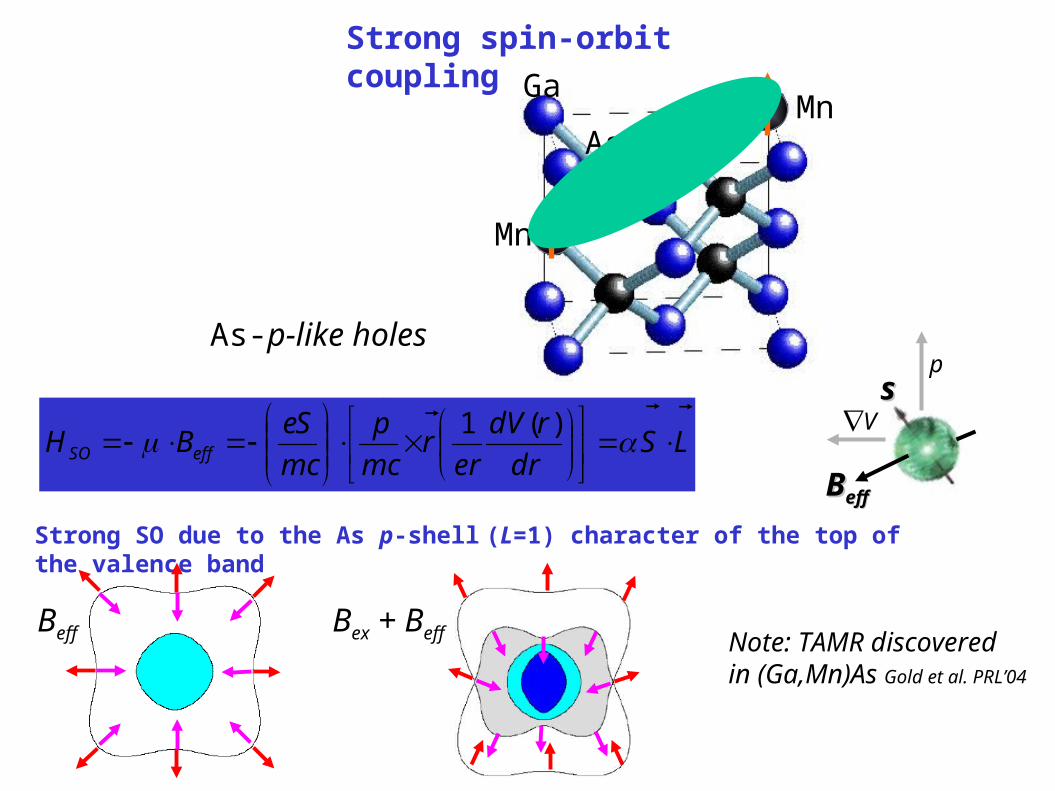
Strong spin-orbit coupling
LSdr
rdV
err
mc
p
mc
SeBH effSO
)(1
Strong SO due to the As p-shell (L=1) character of the top of the valence band
V
BBeffeff
pss
Beff Bex + Beff Note: TAMR discovered in (Ga,Mn)As Gold et al. PRL’04
Mn
Ga
AsMn

(Ga,Mn)As synthesis
Low-T MBE to avoid precipitation
High enough T to maintain 2D growth
need to optimize T & stoichiometry for each Mn-doping
Inevitable formation of interstitial Mn-donorscompensating holes and moments need to anneal out
high-T growth
optimal-T growth

Interstitial Mn out-diffusion limited by surface-oxide
GaMnAs
GaMnAs-oxide
Polyscrystalline20% shorter bonds
MnI++
O
Optimizing annealing-T another key factorRushforth et al, ‘08
x-ray photoemission
Olejnik et al, ‘08
10x shorther annealing with etch

0 1 2 3 4 5 6 7 8 9 100
20
40
60
80
100
120
140
160
180
TC(K
)
Mntotal
(%)
Indiana & California (‘03): “ .. Ohno’s ‘98 Tc=110 K is the fundamental upper limit ..” Yu et al. ‘03
California (‘08): “…Tc =150-165 K independent of xMn>10% contradicting Zener kinetic exchange ...”
Nottingham & Prague (’08): Tc up to 185Kso far
“Combinatorial” approach to growthwith fixed growth and annealing T’s
?Mack et al. ‘08
Tc limit in (Ga,Mn)As remains open

Weak hybrid.Delocalized holeslong-range coupl.
Strong hybrid.Impurity-band holesshort-range coupl.
InSb
GaP
d5
(Al,Ga,In)(As,P) good candidates, GaAs seems close to the optimal III-V host
Other (III,Mn)V’s DMSs
Mean-field butlow Tc
MF
Large TcMF but
low stiffness
Kudrnovsky et al. PRB 07

III = I + II Ga = Li + Zn
Other DMS candidates
Masek et al. PRL 07But Mn isovalent in Li(Zn,Mn)As
no Mn concentration limit and self-compensation
possibly both p-type and n-type ferromagnetic SC
(Li / Zn stoichiometry)
GaAs and LiZnAs are twin SC
(Ga,Mn)As and Li(Zn,Mn)As
should be twin ferromagnetic SC
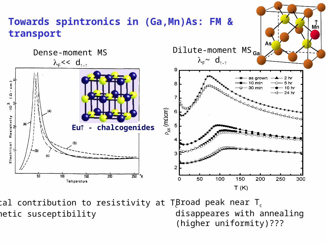
Towards spintronics in (Ga,Mn)As: FM & transport
Dense-moment MSF<< d-
Eu - chalcogenides
Dilute-moment MSF~ d-
Critical contribution to resistivity at Tc
~ magnetic susceptibility
Broad peak near Tc disappeares with annealing (higher uniformity)???

Ni
(Ga,Mn)As (Prague Nottingham)
Fe
Critical contribution at Tc to d/dT like TM FMs
d/dT ~ cv
F ~ d-
Fisher & Langer ’68Novak et al., ‘08
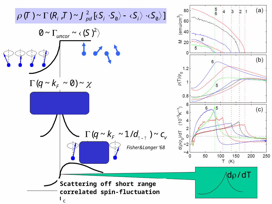
vF cdkq ~)/1~~(
Tc
d/dT
][~),(~)( 002 SSSSJTRT iipdi
2)(~~0 Suncor
~)0~~( Fkq
Scattering off short rangecorrelated spin-fluctuation
Fisher&Langer ‘68

OutlineOutline
11.. Tunneling anisotropic magnetoresistance in transition metals Tunneling anisotropic magnetoresistance in transition metals
2. Ferromagnetism in (Ga,Mn)As and related semiconductors2. Ferromagnetism in (Ga,Mn)As and related semiconductors
3. Spintronic transistors3. Spintronic transistors
0.0 0.5 1.0 1.5 2.0 2.5 3.0 3.5 4.0
0
2
4
6
8
10
0V 3V 5V 10V
carr
ier
dens
ity
[ 10
19 c
m-3
]
GaMnAs layer thickness [nm]
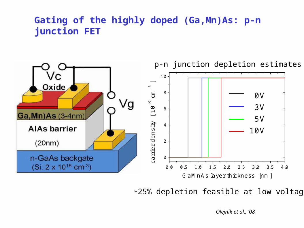
Gating of the highly doped (Ga,Mn)As: p-n junction FET
p-n junction depletion estimates
Olejnik et al., ‘08
~25% depletion feasible at low voltages
20 22 24 26 28 30 32 34
18.6
18.8
19.0
19.2
19.4
[10
-3c
m]
T [K]
Vg = 0V
22.5
23.0
23.5
24.0
24.5 Vg = 3V
20 22 24 26 28 30 32 34
-200
-100
0
100
d/d
T [1
0-6
T [K]
-300
-200
-100
0
AM
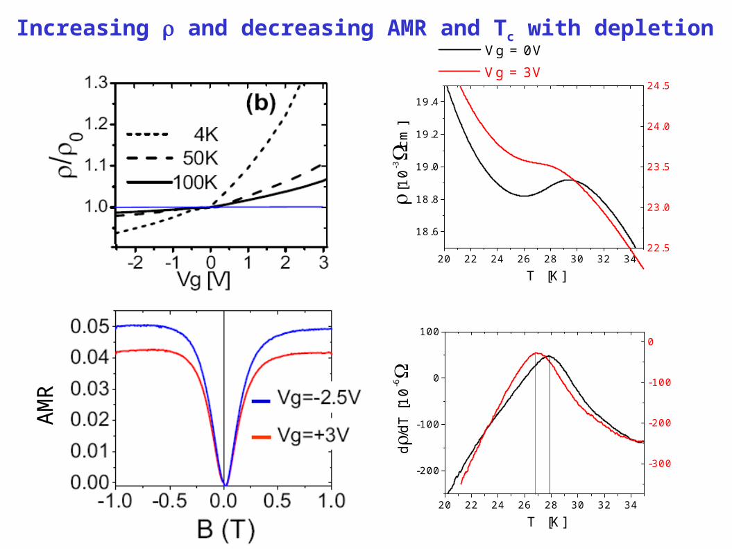
RIncreasing and decreasing AMR and Tc with depletion
30 40 50 60 70 80 90 100
100
200
65K62K
dR/d
T
T (K)
depletion accumulation
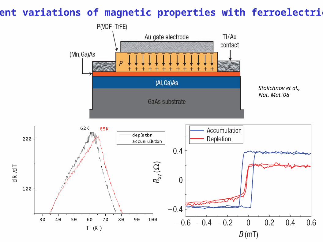
Persistent variations of magnetic properties with ferroelectric gates
Stolichnov et al., Nat. Mat.‘08

exy = 0.1%
exy = 0%
Electro-mechanical gating with piezo-stressors
Rushforth et al., ‘08
Strain & SO
Electrically controlled magnetic anisotropies
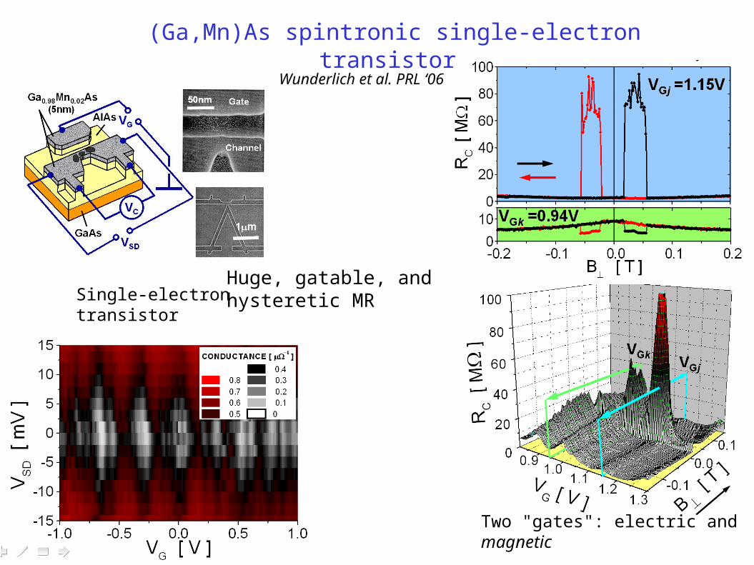
Single-electron transistor
Two "gates": electric and magnetic
(Ga,Mn)As spintronic single-electron transistor
Huge, gatable, and hysteretic MR
Wunderlich et al. PRL ‘06
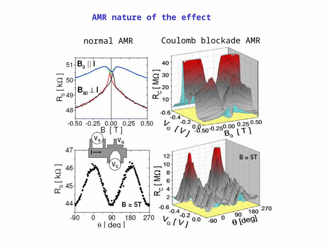
AMR nature of the effect
normal AMR Coulomb blockade AMR

GMMGG0
20
C
C
e
)M(V&)]M(VV[CQ&
C2
)QQ(U
electric && magneticmagnetic
control of Coulomb blockade oscillations
n-1 n n+1 n+2n-1 n n+1 n+2
EC
QQindind = = nnee
QQindind = (= (n+1/2)n+1/2)eeQ0
Q0
e2/2C
Q
0
'D
'
e
)M(Q)Q(VdQU
[010]
M[110]
[100]
[110][010]
SO-coupling (M)
Source Drain
GateVG
VDQ
Single-electron charging energy controlled by Vg and M

• CBAMR if change of |CBAMR if change of |((MM)| ~ )| ~ ee22//22CC
• In our (Ga,Mn)As ~ meV (~ 10 Kelvin)In our (Ga,Mn)As ~ meV (~ 10 Kelvin)
• In room-T ferromagnet change of |In room-T ferromagnet change of |((MM)|~100K )|~100K
• Room-T conventional SET (e2/2C >300K) possible
Theory confirms chemical potential anisotropies in (Ga,Mn)As& predicts CBAMR in SO-coupled room-Tc metal FMs

Variant p- or n-type FET-like transistor in one single nano-sized CBAMR device
0
ONONOFFOFF
1
0
ONON OFFOFF
1
VDD
VA VB
VA
VB
Vout
0
0
0
OFFOFFONON
ONON
OFFOFF
0
0
1
1
ONONOFFOFF
A B Vout0 0 01 0 10 1 11 1 1
0
01
ONON
OFFOFF
0
0
OFFOFF
1
ONON
1
1
1
1
OFFOFF
ONON
1
1
ONON
OFFOFF
1
“OR”
Nonvolatile programmable logic
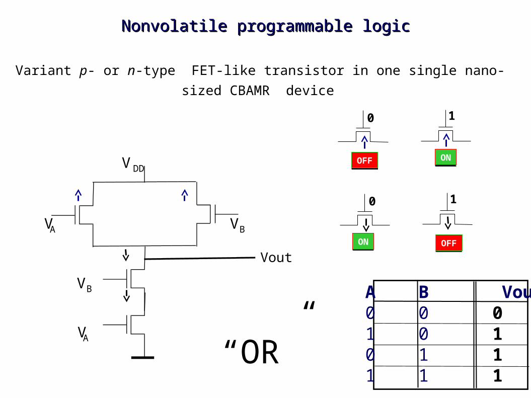
VDD
VA VB
VA
VB
Vout
Variant p- or n-type FET-like transistor in one single nano-sized CBAMR device
0
ONONOFFOFF
1
0
ONON OFFOFF
1
A B Vout0 0 01 0 10 1 11 1 1
“OR”
Nonvolatile programmable logicNonvolatile programmable logic
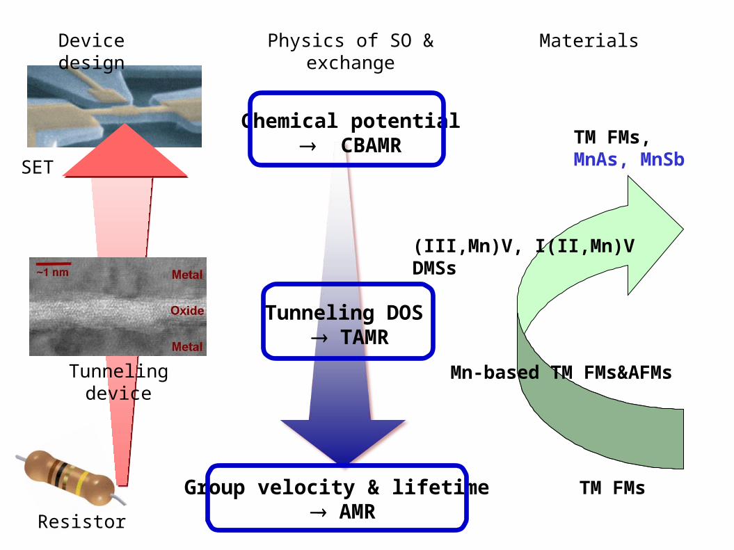
Physics of SO & exchange
SET
Resistor
Tunneling device
Chemical potential CBAMR
Tunneling DOS TAMR
Group velocity & lifetime AMR
Device design Materials
TM FMs
(III,Mn)V, I(II,Mn)VDMSs
Mn-based TM FMs&AFMs
TM FMs,MnAs, MnSb

END

Dawn of spintronicsDawn of spintronics
Anisotropic magnetoresistance (AMR) – 1850’s Anisotropic magnetoresistance (AMR) – 1850’s 1990’s 1990’s
Giant magnetoresistance (GMR) – 1988 Giant magnetoresistance (GMR) – 1988 1997 1997
Inductive read/write element
Magnetoresistive read element
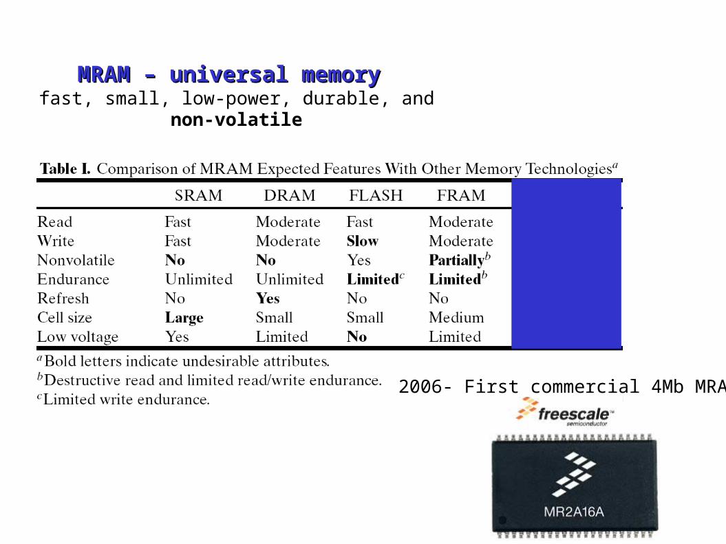
MRAM – universal memoryMRAM – universal memory fast, small, low-power, durable, and non-volatile
2006- First commercial 4Mb MRAM
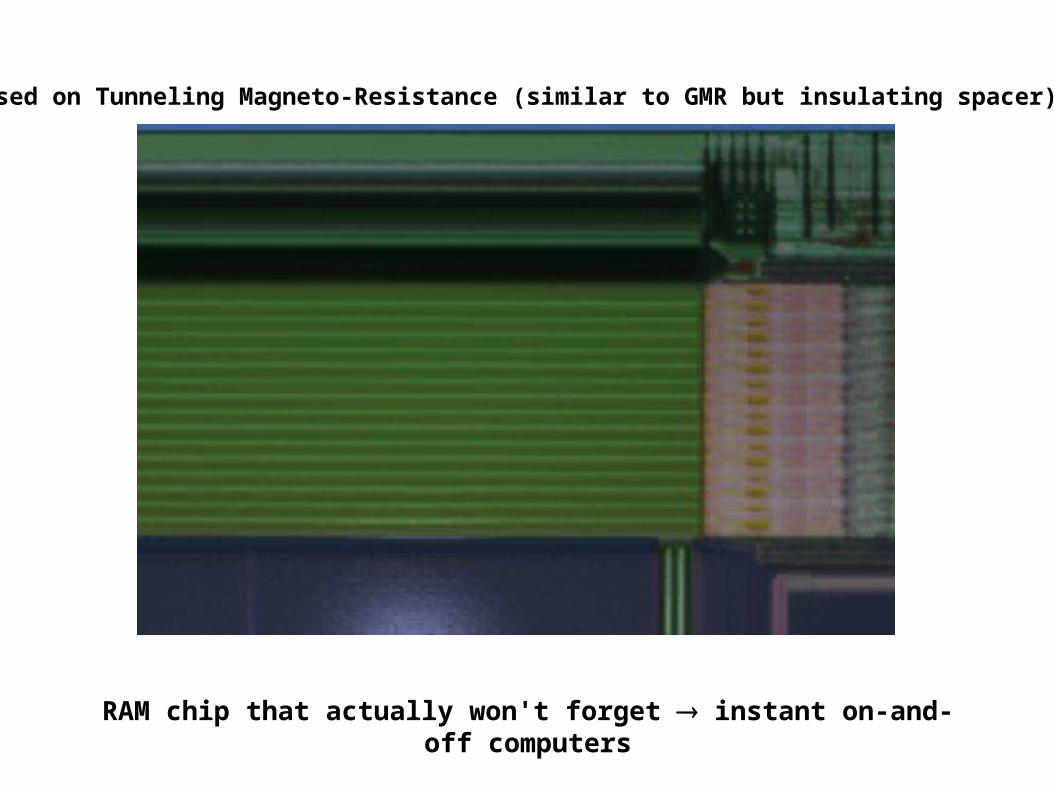
RAM chip that actually won't forget instant on-and-off computers
Based on Tunneling Magneto-Resistance (similar to GMR but insulating spacer)
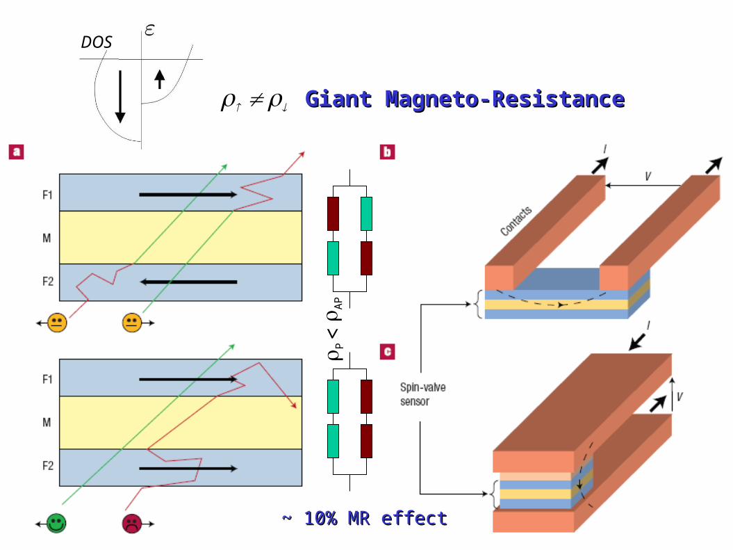
Giant Magneto-ResistanceGiant Magneto-Resistance
~ 10% MR effect~ 10% MR effect
DOS
AP
P
>
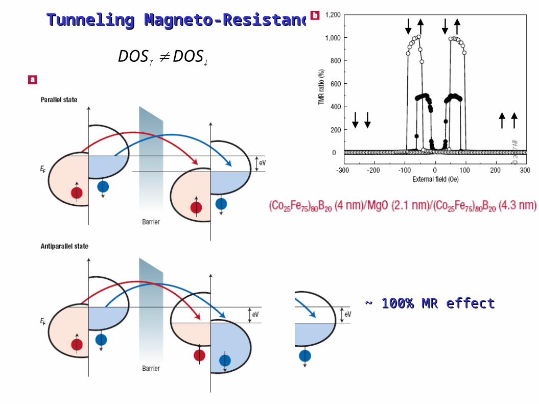
Tunneling Magneto-ResistanceTunneling Magneto-Resistance
~ 100% MR effect~ 100% MR effect
DOS DOS

Spin Transfer Torque writingSpin Transfer Torque writing
GaAs Mn
Mn
10-100x smaller Ms
One
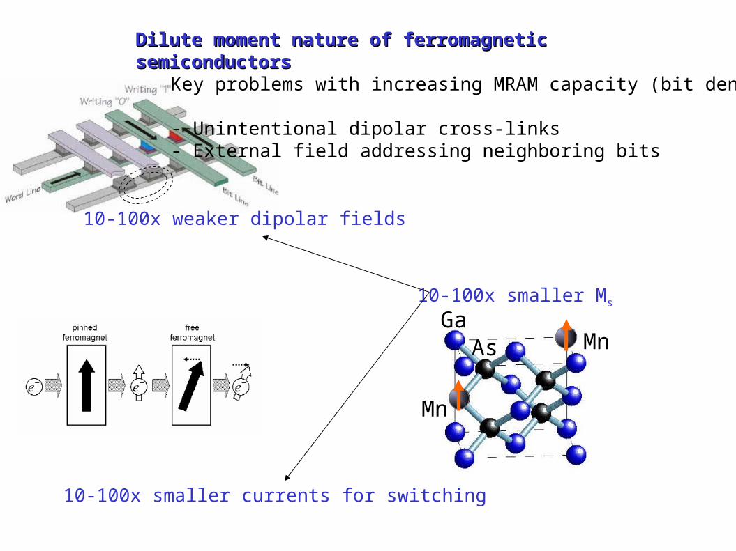
Key problems with increasing MRAM capacity (bit density):
- Unintentional dipolar cross-links- External field addressing neighboring bits
10-100x weaker dipolar fields
10-100x smaller currents for switching
Dilute moment nature of ferromagnetic semiconductorsDilute moment nature of ferromagnetic semiconductors

Magnetism in systems with coupled dilute moments and delocalized band electrons
(Ga,Mn)As
cou
pli
ng
str
eng
th /
Fer
mi
ener
gy
band-electron density / local-moment density
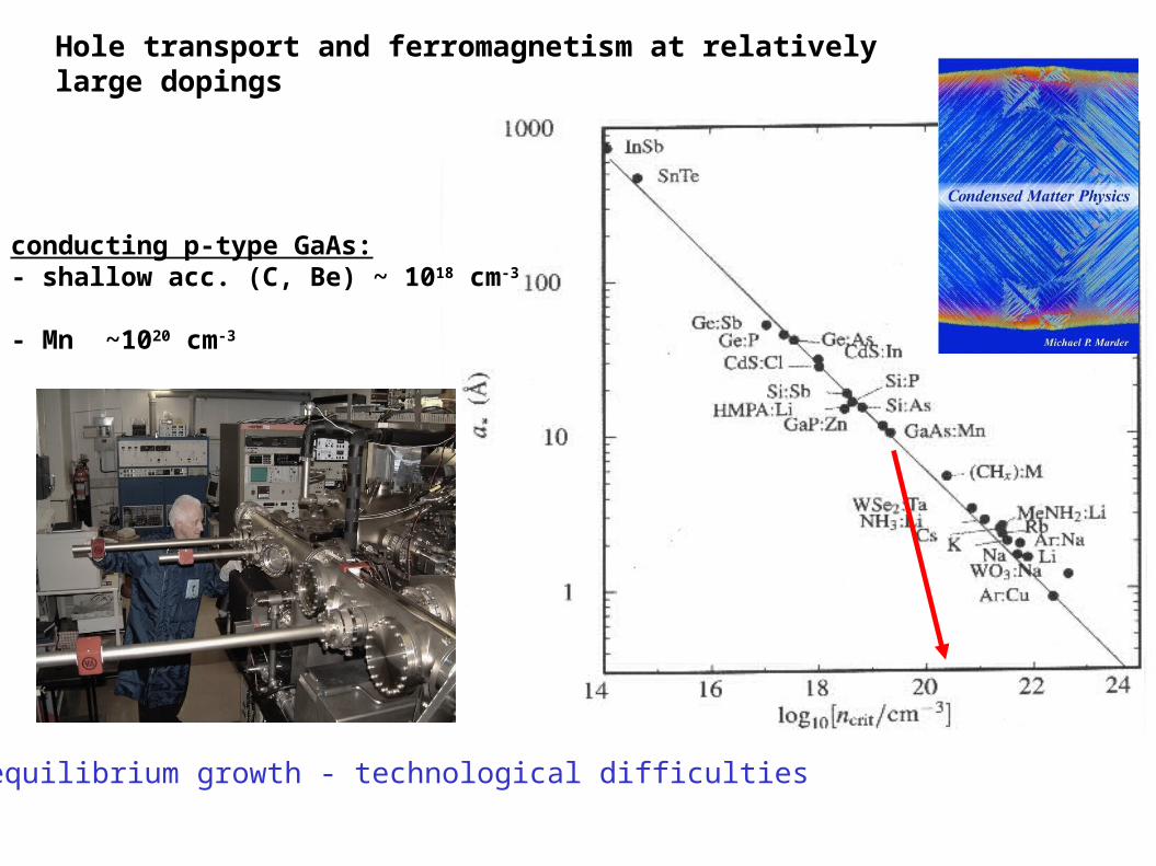
Hole transport and ferromagnetism at relatively large dopings
conducting p-type GaAs:- shallow acc. (C, Be) ~ 1018 cm-3
- Mn ~1020 cm-3
Non-equilibrium growth - technological difficulties

Electric-field controlledferromagnetism in FET or piezo/FM hybrid
Vgate
Ferro SC
Photogenerated ferromagnetism
Ferro SC
GaSb
B (mT)
ħ
Mag
net
izat
ion
Mag
net
izat
ion

Variable controlled strain using a Piezo stressor A.W. Rushforth, J. Zemen, K. Vyborny, et al. arXiv:0801.0886
Strain induced by piezo voltage +/- 150V:
~ 2 10-4 (at 50K)
Easy axis rotation by
50 deg for
Vpiezo = -150V +150V
M. Overby, et al., arXiv:0801.4191
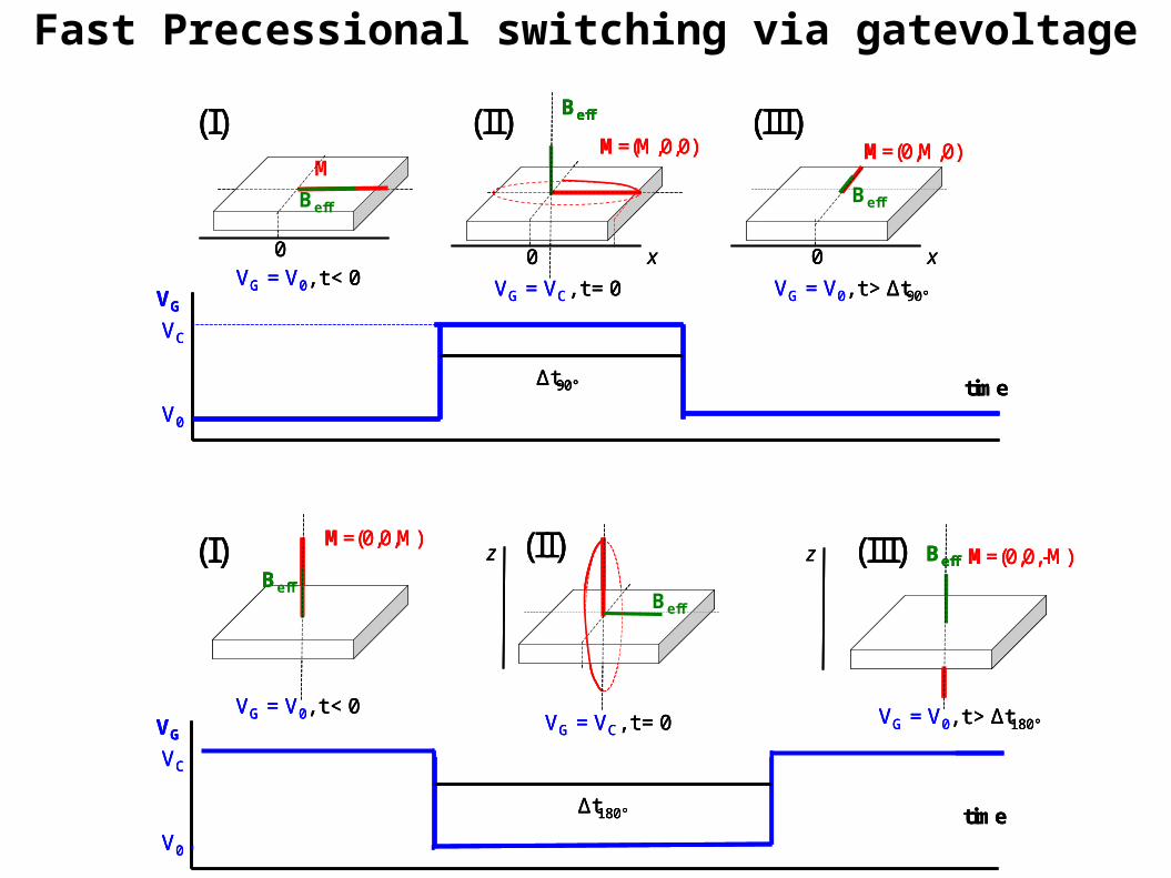
Beff
VG = V0, t < 0VG
timeV0
VC
Δt180°
Beff
VG = VC, t = 0
zM=(0,0,M)
Beff
VG = V0, t > Δt180°
M=(0,0,-M)z(I) (II) (III)
M
Beff
VG = V0, t < 0
(I)
VG
timeV0
VC
Δt90°
Beff
VG = VC, t = 0
(II)
0 x
M=(M,0,0)
Beff
VG = V0, t > Δt90°
(III)
0 x
M=(0,M,0)
0
(a)
(b)
Beff
VG = V0, t < 0VG
timeV0
VC
Δt180°
Beff
VG = VC, t = 0
zM=(0,0,M)
Beff
VG = V0, t > Δt180°
M=(0,0,-M)z(I) (II) (III)
M
Beff
VG = V0, t < 0
(I)
VG
timeV0
VC
Δt90°
Beff
VG = VC, t = 0
(II)
0 x
M=(M,0,0)
Beff
VG = V0, t > Δt90°
(III)
0 x
M=(0,M,0)
0
(a)
(b)
Beff
VG = V0, t < 0VG
timeV0
VC
Δt180°
Beff
VG = VC, t = 0
zM=(0,0,M)
Beff
VG = V0, t > Δt180°
M=(0,0,-M)z(I) (II) (III)
M
Beff
VG = V0, t < 0
(I)
VG
timeV0
VC
Δt90°
Beff
VG = VC, t = 0
(II)
0 x
M=(M,0,0)
Beff
VG = V0, t > Δt90°
(III)
0 x
M=(0,M,0)
0
(a)
(b)
Fast Precessional switching via gatevoltage
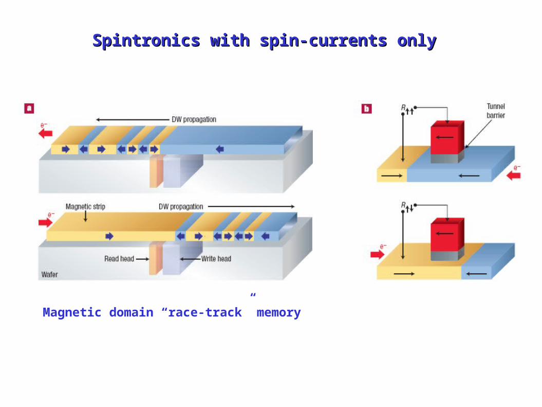
Spintronics with spin-currents onlySpintronics with spin-currents only
Magnetic domain “race-track” memory

n
n
p
SHE mikročip, 100A supercondicting magnet, 100 A
Spin Hall effect detected optically in GaAs-based structures
Same magnetization achievedby external field generated bya superconducting magnet with 106 x larger dimensions & 106 x larger currents
Cu
SHE detected elecrically in metals SHE edge spin accumulation can beextracted and moved further into the circuit

Datta-Das transistor
Spintronics in nominally non-magnetic materialsSpintronics in nominally non-magnetic materials
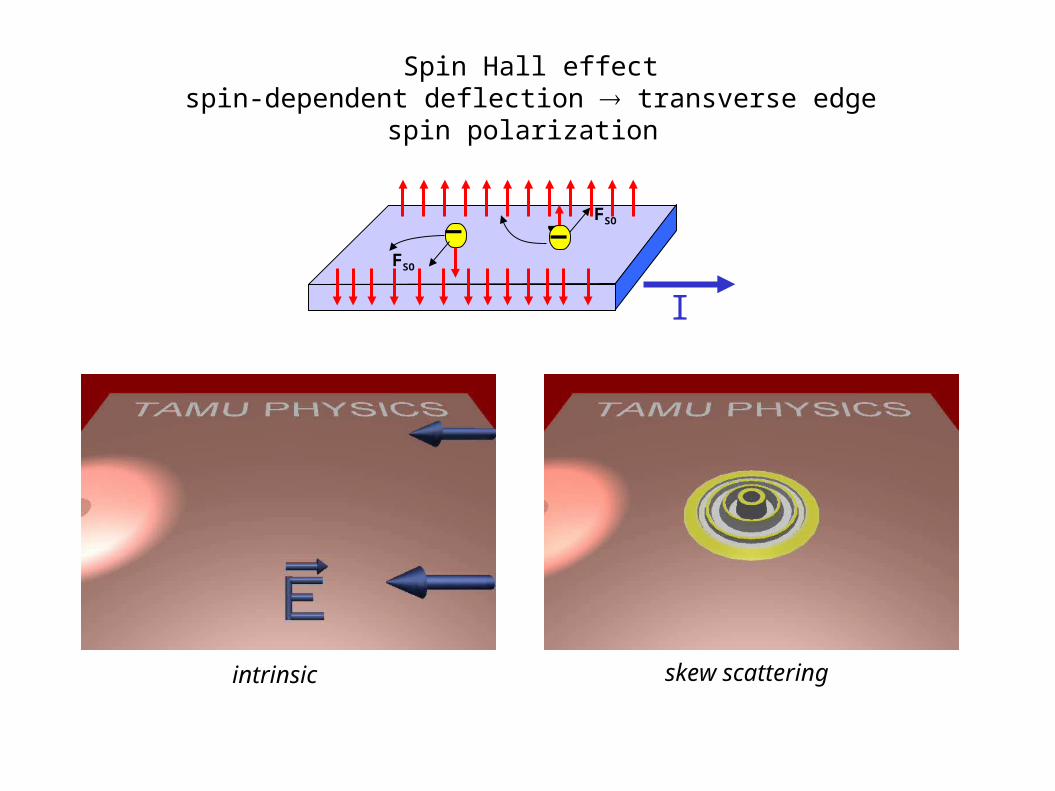
intrinsic skew scattering
I
_ FSO
FSO
_ __
Spin Hall effectspin-dependent deflection transverse edge spin polarization
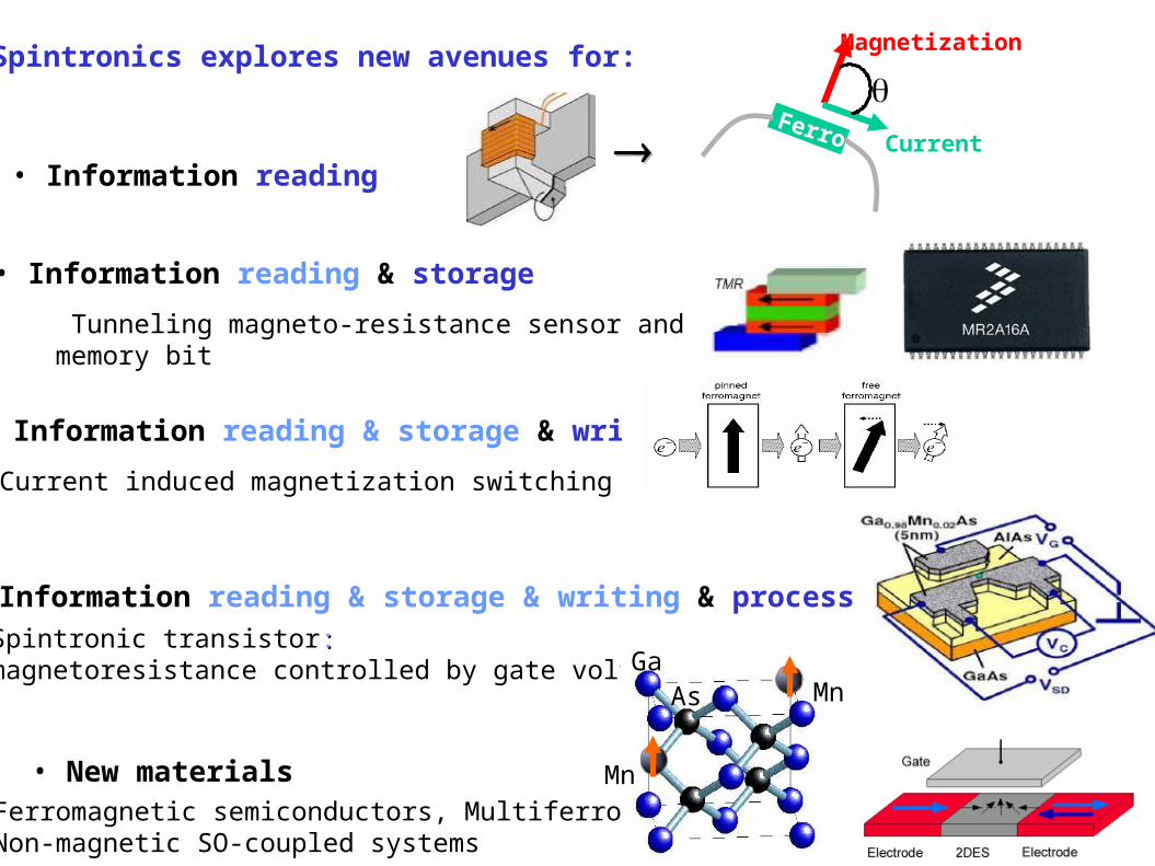
• Information reading
Ferro
Magnetization
Current
• Information reading & storage
Tunneling magneto-resistance sensor and memory bit
• Information reading & storage & writing
Current induced magnetization switching
• Information reading & storage & writing & processing
Spintronic transistor::magnetoresistance controlled by gate voltage
• New materialsFerromagnetic semiconductors, MultiferroicsNon-magnetic SO-coupled systems
Mn
GaAs Mn
Spintronics explores new avenues for:
Related Documents


![Modern Marketing in Oil & Gas - Jason Rushforth [Oracle Marketing Cloud]](https://static.cupdf.com/doc/110x72/587f8df51a28ab28518b60d9/modern-marketing-in-oil-gas-jason-rushforth-oracle-marketing-cloud.jpg)