1 Spintronic and optoelectronic devices using topological insulators and Dirac/Weyl materials Hyunsoo Yang Electrical and Computer Engineering, National University of Singapore [email protected] Outline • Nanoelectronics overview • Graphene magnetic sensors • Graphene optoelectronics (THz devices) • Spin-orbit torque (SOT) engineering – AHE & SOT in LaAlO 3 /SrTiO 3 oxide heterostructures – SOT in topological insulators (Bi 2 Se 3 /ferromagnet) • Topological insulator spin detectors • Weyl spin lifetime measurements 2

Welcome message from author
This document is posted to help you gain knowledge. Please leave a comment to let me know what you think about it! Share it to your friends and learn new things together.
Transcript

1
Spintronic and optoelectronic devices using topological insulators and Dirac/Weyl materials
Hyunsoo Yang
Electrical and Computer Engineering, National University of Singapore
Outline
• Nanoelectronics overview
• Graphene magnetic sensors
• Graphene optoelectronics (THz devices)
• Spin-orbit torque (SOT) engineering
– AHE & SOT in LaAlO3/SrTiO3 oxide heterostructures
– SOT in topological insulators (Bi2Se3/ferromagnet)
• Topological insulator spin detectors
• Weyl spin lifetime measurements
2

2
Electron, photon, and spin
• Electronics– Transistor – small wavelength
– FLASH memory – long trapping time
• Photonics– Optical fiber communication – long distance
– Not compatible with nanoelectronic due to wavelength difference (diffraction limit)
• Spintronics– Information can be stored in magnetic materials.
– Not easy to send for a long distance.
3
Grand challenges in electronics
4

3
Emergence of electronics
5
A difficult problem
The ICs operate in incredibly harsh conditions, turning on and off trillions of time during its lifetime
1 CPU ~ 109 Transistors
When one transistor fails, so does the IC
6
Uniformity issue is the challenge any new materials including graphene and 2D materials will face!

4
Transistor scaling (lateral)
Devices are getting very small. Will they reach quantum or even atomic dimensions? What principles will they operate on? Still charge or is spin or something else possible?
7
Jim Plummer
8
Thinner and thinner (vertical scaling)
graphitegraphene
solid lubricantMoS2
Bi2Te3 and Bi2Se3
Wine cooler
beveragefactory.com Physics 3, 62 (2010)
Topological insulators

5
Graphene applications
9Sensors, optoelectronics (THz)
10
Why Silicon?
• SiO2 is a Magical Material• SiO2 passivates the surface of Si• SiO2 is an excellent insulator• SiO2 is an excellent barrier against impurity diffusion• SiO2 has very high etch selectivity to Si
• Si is easily purified and can be grown defect free single crystal• Si has reasonably good electronic properties which produce a
variety of devices with excellent performance• Si and SiO2 are tolerant to a variety of harsh environments
used in fabrication and is highly manufacturable• Si has excellent mechanical properties which facilitate handling
and manufacturing• Si is readily available and very plentiful in nature
6
11
Voltage controlled vs. current controlled
metal oxide semiconductor (MOS) Spin transfer torque (STT)
Voltage controlled (capacitive coupling)Suitable for parallel connection
current controlledSuitable for serial connection
Spin devices may not require an oxide layerNeed different approach
12
Metal ions and alkali ions must be removed from Si device active regions
7
13
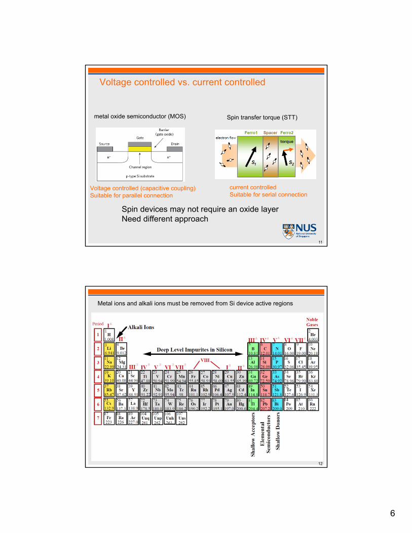
Technologically accessible photonic materials
Mostly single or binary element (solid state chemists are way ahead!)Silicon cannot emit light, but works as photodetectors (PDs)
Topological insulators and Weyl spin selective PDs
14
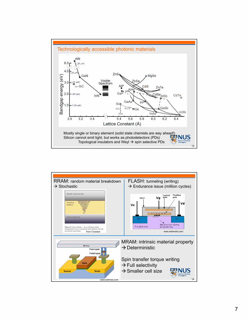
RRAM: random material breakdown Stochastic
MRAM: intrinsic material propertyDeterministic
Spin transfer torque writingFull selectivitySmaller cell size
from Crossbar
FLASH: tunneling (writing) Endurance issue (million cycles)
www.eeherald.com/
www.eetimes.com
8
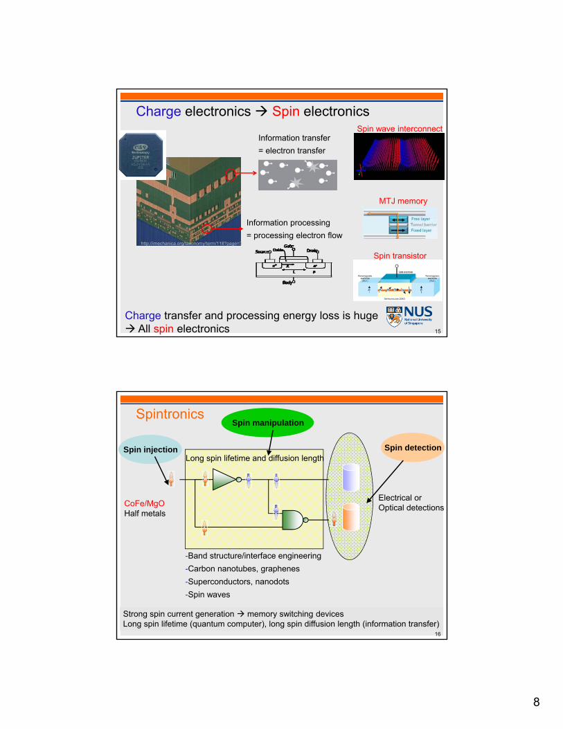
Charge electronics Spin electronics
Information transfer
= electron transfer
Information processing
= processing electron flow
Charge transfer and processing energy loss is huge All spin electronics
http://imechanica.org/taxonomy/term/118?page=3
15
Spin wave interconnect
Spin transistor
MTJ memory
Spintronics
-Band structure/interface engineering
-Carbon nanotubes, graphenes
-Superconductors, nanodots
-Spin waves
Spin injection Spin detection
Spin manipulation
CoFe/MgOHalf metals
Electrical orOptical detections
Long spin lifetime and diffusion length
16
Strong spin current generation memory switching devicesLong spin lifetime (quantum computer), long spin diffusion length (information transfer)

9
20
MTJ read sensors in HDD
We understand MTJ sensor very well Building high density MTJ array for MRAM is a different story
GMR ~ 10%TMR ~ 50%
24
Magnetic sensor applications

10
25
Magnetic sensors in a car
Copyright 2012 IHS Inc.
Graphene magnetic sensors
26
-10 -8 -6 -4 -2 0 2 4 6 8 10
0
100
200
300
400
500
MR
(%
)
0H (T)
1.9 20 50 100 150 200 250 300
Vg=0V, 30uA
T (K)
Temperature insensitive giant magneto-resistance (MR)Gate tunable propertyGiant MR is explained by inhomogeneous charge distribution
Phys. Rev. B 88, 195429 (2013)

11
Systems showing linear MR
1. InSb
2. Ag2Te and Ag2Se
3. (Multilayer) graphene
4. TI (Bi2Se3, Bi2Te3)
5. Weyl-WTe2
Theoretical explanation of linear MR• Classical model
• Quantum model
Nature 390, 57 (1997)
Nature 426, 162 (2003)
PRB 58, 2788 (1998)
Nat. Mater. 7, 697 (2008), Science 289, 1530 (2000)
Nat. Comm. 6, 8337 (2015), Phys. Rev. B 88, 195429 (2013)Nano Lett. 10, 3962 (2010)
APL 102, 012102 (2013), PRL 108, 266806 (2012)
Nature 514, 205 (2014)
28
Classical model
Inhomogeneity
Random resistor network
Local mobility fluctuations
Linear MR(temperature independent)
Nature 426, 162 (2003), Nature 477, 304 (2011)29

12
Quantum model
Abrikosov, A. A. Quantum magnetoresistance. Physical Review B 58, 2788 (1998)
Tail
Inhomogeneity
Tail formation
Linear E-k
Linear MR(temperature independent)
Low band-gap + small eff. mass
ħω > EF
30
Two channel model
Large mobility difference is important for a large MR
38
1)( 2
12
21
21
nn
nnMR
Case I
Case II
Case III
Nat. Comm. 6, 8337 (2015)
High sensitivity at low field is important for applications
13
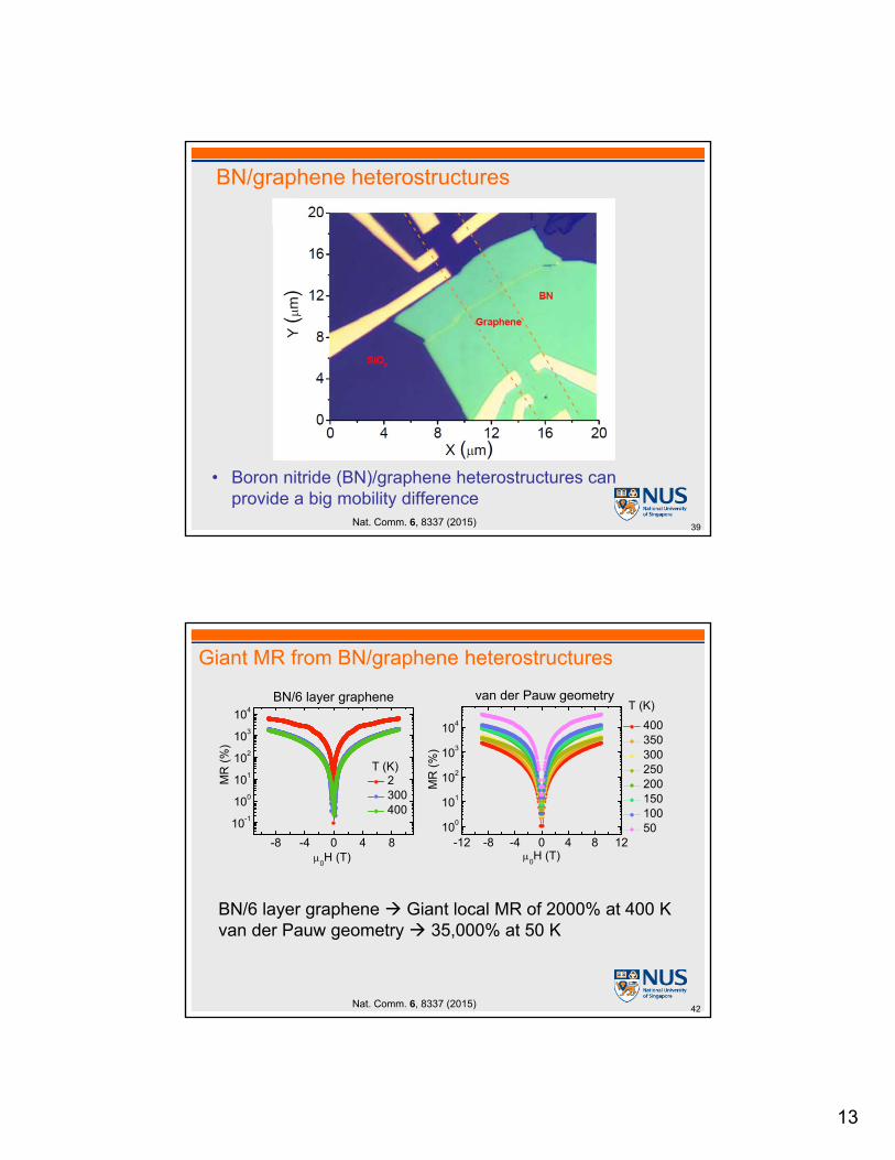
BN/graphene heterostructures
• Boron nitride (BN)/graphene heterostructures can provide a big mobility difference
39Nat. Comm. 6, 8337 (2015)
Giant MR from BN/graphene heterostructures
42
-8 -4 0 4 8
10-1
100
101
102
103
104
-12 -8 -4 0 4 8 12100
101
102
103
104
T (K)
MR
(%
)
0H (T)
2 300 400
MR
(%
)
0H (T)
400 350 300 250 200 150 100 50
T (K)
BN/6 layer graphene Giant local MR of 2000% at 400 K van der Pauw geometry 35,000% at 50 K
Nat. Comm. 6, 8337 (2015)
BN/6 layer graphene van der Pauw geometry

14
Non-local MR
43
4 layer graphene/BN at 300 K
non-local MR value of 90,000%
Ettingshausen-Nernst effect
Nat. Comm. 6, 8337 (2015)
Graphene applications
44THz

15
Applications of Terahertz Light
55
Giant THz machine
56
-We need to miniaturize big THz machine.-For this we need various small THz devices,
such as phase shifters, modulators, generators, etc.

16
Problems in conventional THz phase shifters
57
Chen C. Y. et al. Magnetically tunable room-temperature 2π liquid crystal terahertz phase shifter. Optical Express. (2004)
Hsieh C. F. et al. Voltage-controlled liquid-crystal terahertz phase shifter and quarter-wave plate. Optical Letters. (2006)
Bulky magnets required High voltage (200 V) required
Schematic diagram of the THz phase shifters
58
With bias voltageWithout applying voltage
:polyimide
Optics Express 21, 21395 (2013)
17
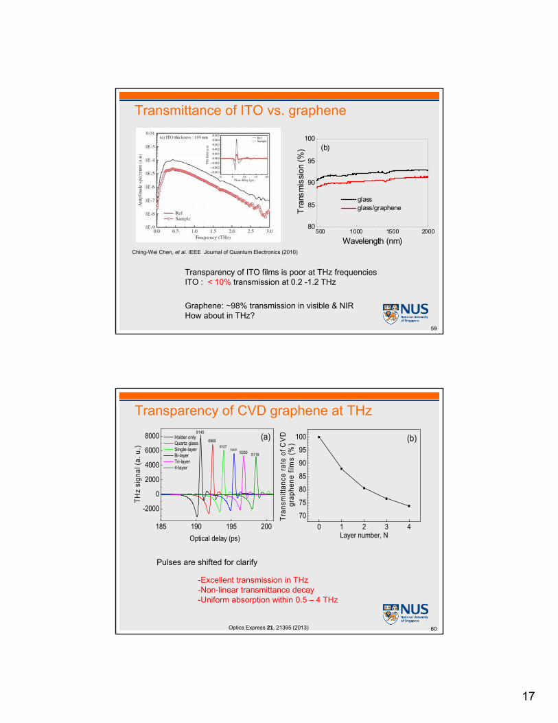
Transmittance of ITO vs. graphene
59
Ching-Wei Chen, et al. IEEE Journal of Quantum Electronics (2010)
Transparency of ITO films is poor at THz frequenciesITO : < 10% transmission at 0.2 -1.2 THz
500 1000 1500 200080
85
90
95
100
(b)
Tra
nsm
issi
on (%
)
Wavelength (nm)
glass glass/graphene
Graphene: ~98% transmission in visible & NIRHow about in THz?
Transparency of CVD graphene at THz
60
-Excellent transmission in THz-Non-linear transmittance decay-Uniform absorption within 0.5 – 4 THz
Pulses are shifted for clarify
185 190 195 200
-2000
0
2000
4000
6000
8000 Holder only Quartz glass Single-layer Bi-layer Tri-layer 4-layer
6960
TH
z si
gnal
(a.
u.)
Optical delay (ps)
8140
6127
5330 5119
(a)
0 1 2 3 4
70
75
80
85
90
95
100 (b)
Tra
nsm
ittan
ce r
ate
of C
VD
gra
phen
e fil
ms
(%)
Layer number, N
Optics Express 21, 21395 (2013)

18
THz phase shift measurements
62
190 200 210 220 230-800
-400
0
400
800
1200
0 1 2 3 4 5 6 7 8 9
0
2
4
6
8
10
12
TH
z si
gn
al (
a.u
.)
Time Delay (ps)
201.02 201.04 201.06 201.08 201.10
330
335
340
345 0.0 V 1.0 V 2.0 V 3.0 V 4.0 V 5.0 V
TH
z si
gnal
(a.
u.)
Time Delay (ps)
Pha
se s
hift
(de
gree
)
Bias Voltage (V)
0.25 THz 0.75 THz 0.50 THz 1.00 THz
Voltage controlled phase shiftsTHz time delay under different bias voltages
Optics Express 21, 21395 (2013)
Low bias voltage operation (~ 5 V for saturation). Linear controllability in low bias voltages.
Graphen/ionic liquid THz modulation
64
2 2( ) ( ) / (1 )DC FE
Utilizing intra-band absorption
Adv. Mat. 27, 1874 (2015)
0.0 0.5 1.0 1.5 2.0 2.5 3.0
0.2
0.4
0.6
0.8
1.0 Tri-layer graphene
Tra
nsm
ittanc
e
Voltage (V)

19
0 1 2 30.2
0.4
0.6
0.8
1.0 100 m cell 50 m cell
Tra
nsm
itta
nce
Gate voltage (V)0 1 2 3
0.0
0.3
0.6
0.9
1.2
Tra
nsm
itta
nce
Gate voltage (V)
Single-layer Bi-layer Tri-layer Double-deck
Geometry & layer thickness dependence study
Modulators with 50 µm & 100 µm ionic liquid cells
Multilayer & double-deck modulators
Transmittance• Mono-layer 83%• Bi-layer 89%• Tri-layer 93%• Double deck 99%
Similar modulation depth for devices with different cell thickness
Adv. Mat. 27, 1874 (2015)67
75
Logic device (switch) applications
For switch applications, on/off current ratio should be
(TFT panel) > 100, Conventional logic CMOS > 1000
Need to increase TMR (Need a high spin polarization)
New material for electrodes and barriers
- MgO spin filter (on/off ration < 10)
- Half metals (only at low temp.)
1 2
1 2
2
1AP P
P
R R PPMR
R PP
MgO (100)
s∆2,5 ∆1
Fe
Fe

20
Almost perfect switches/filters nonreciprocity
76
Mechanical switchTransistor
Optical filter Microwave circulator
Is there any similar component in spintronics?
Describing spin wavesSingle electron spin
1D chain of (dipolar/exchange) coupled electrons
Collective magnetization dynamics: spin waves
FMRUniform precession (standing waves)
Spin wavesTravelling waves
77

21
78
-z
z
y
xLNA
bias field (Hz)
Pulse generator
Sampling oscilloscope
tTa (Ta thickness) ranges from 0 to 10 nm
Measurements set-up and layer structure of spin wave device
< stack of layers >
79
Giant nonreciprocal emission of spin wave in Ta/Py
-100
10
-100
10
-100
10
2 4 6 8-10
010
2 4 6 8 2 4 6 8
Hz = +258 Oe Hz = -258 Oe0 nm
0.9 nm
1.8 nm
2.7 nm
volta
ge (
mV
)
3.6 nm
4.6 nm
5.5 nm
6.4 nm
7.3 nm
8.2 nm
9.1 nm
time (ns)
10 nm
- The amplitude at -258 Oe is higher than that at +258 Oe in the device for 0 < tTa < 2.7 nm.- However, the amplitude at +258 Oe is higher than that at -258 Oe for 4.6 nm < tTa < 10 nm
ON / OFF ratio of 60

22
80
V
y
x
‐Hz+Hz
2 4 6 8 10
0
10
20
30
40
V-sp
V+sp
Vsp
(V
)
tTa (nm)
1
2
3
4
1
0-3
Giant nonreciprocity due to spin pumping
Hall effect & spin Hall effect (SHE)
82
SHE: Separate electrons of different spins without using a magnetic field
Y.K. Kato, Sci. Am. 2007

23
83
Miron et al. Nature 476, 189 (2011)
• Heavy metal/ferromagnetic material/oxide layer.• Current induced magnetization switching is observed (longitudinal field
needed).• Magnetization states depend on both current and field directions.• Possible mechanisms: Rashba effect & spin Hall effect (SHE).
Spin-orbit torques (SOT)
Liu et al. PRL 109, 096602 (2012)
Perpendicularly magnetized trilayer structures
Heavy Metal (HM)
Ferromagnet(FM)
OxideStrong Rashba field arises from asymmetric interfaces
Spin Hall effect arises from HM
M
In-plane currents can switch the magnetization
FM1
MgO
FM2
STT
SOT
85

24
Spin Hall angle (SH)
Spin currents can be very large, as the electron can interact with the FM many times (lateral scattering)
87
Heavy metal (HM)
Ferromagnet (FM)
IC
IS
)(c
SSHSH
C
S
t
l
I
I
STT
SOT
t
l
l >> t
Spin Hall angle is a material parameter
88
PRL 112, 197201 (2014), Phys. Rev. B 77, 165117 (2008), Phys. Rev. B 83, 174405 (2011)
Number of d-electrons
Luckily some CMOS compatible materials show large spin Hall angles.
Heavy Weyl semimetals strong spin orbit coupling
25
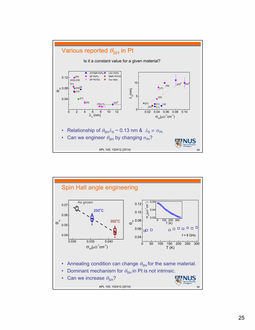
Various reported SH in Pt
• Relationship of SHS ~ 0.13 nm & S Pt
• Can we engineer SH by changing Pt?
89
0 2 4 6 8 10 12
0.04
0.08
0.12[24] [29]
STFMR Pt/Py
SP Pt/Py
SP Pt/YIG[30]
LSV Pt/Py
SMR Pt/YIG
Our data
[9]
[22]*[17][16]
[27]
[20]
[10]
[26]
[21]
sh
s (nm)
0.02 0.04 0.06 0.08 0.100
5
10[36]
[31]
[44]*
[17]
[10]
[22]*
[20]
[27]
[11][24]
s(n
m)
Pt(-1
cm-1)
APL 105, 152412 (2014)
Is it a constant value for a given material?
Spin Hall angle engineering
• Annealing condition can change SH for the same material.
• Dominant mechanism for SH in Pt is not intrinsic.
• Can we increase SH?
90
0.030 0.035 0.040
0.04
0.05
0.06
0.07
250oC
350oC
m
Pt(-1
cm-1)
As grown
0 50 100 150 200 250 300
0.04
0.06
0.08
0.10
0.12
T (K)
m
f = 8 GHz
0 100 200 3000.03
0.04
0.05
T (K)
Pt(
-1cm
-1)
APL 105, 152412 (2014)

26
Spin Hall vs. interfacial Rashba
-Sign of spin Hall angle changes across a transition thickness of SiO2 (t = 1.5 nm) -Cannot be understood by spin Hall physics suggest the role of interface
91Nat. Nanotech. 10, 333 (2015)
0SH
0SH
Reverse switching polarity by oxygen engineering
Spin-orbit torque switching currents
99
S FM HMc eff
SH
e M t AI H
-No damping term great flexibility for choosing FM, high speed
-No spin polarization term no need to use MgO
-Can use thick MgO eliminate MgO breakdown issue
-Large spin Hall angle (SH) or effective field (Heff) is the key
K.J.Lee, APL (2013)
Pinned FM
spacer
Free FM
I1
I2
SOT
STT
2 Sc eff
e M VI H
P
STT
SOT
Heff = ħSH|je|/(2|e|MStF)
27
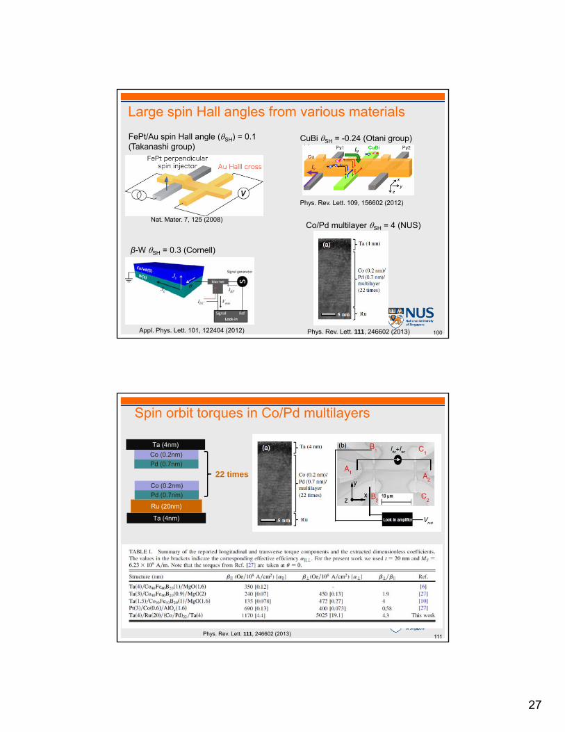
Large spin Hall angles from various materials
100
FePt/Au spin Hall angle (SH) = 0.1(Takanashi group)
Nat. Mater. 7, 125 (2008)
Appl. Phys. Lett. 101, 122404 (2012)
β-W SH = 0.3 (Cornell)
CuBi SH = -0.24 (Otani group)
Phys. Rev. Lett. 109, 156602 (2012)
Co/Pd multilayer SH = 4 (NUS)
Phys. Rev. Lett. 111, 246602 (2013)
111
Spin orbit torques in Co/Pd multilayers
22 times
Ta (4nm)
Ru (20nm)
Pd (0.7nm)
Co (0.2nm)
Pd (0.7nm)
Co (0.2nm)
Ta (4nm)
Phys. Rev. Lett. 111, 246602 (2013)
28
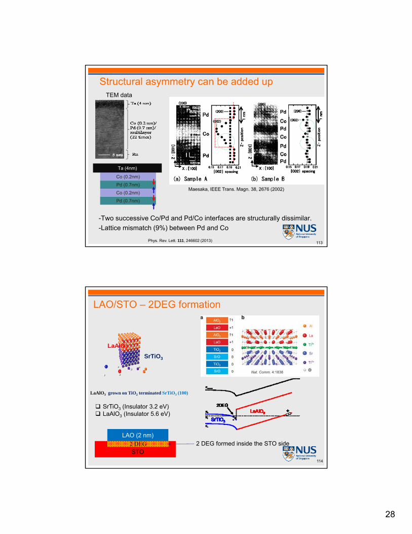
Structural asymmetry can be added up
-Two successive Co/Pd and Pd/Co interfaces are structurally dissimilar.
-Lattice mismatch (9%) between Pd and Co
113
TEM data
Pd (0.7nm)
Co (0.2nm)
Pd (0.7nm)
Co (0.2nm)
Ta (4nm)
Maesaka, IEEE Trans. Magn. 38, 2676 (2002)
Phys. Rev. Lett. 111, 246602 (2013)
LAO/STO – 2DEG formation
114
LaAlO3
SrTiO3
SrTiO3 (Insulator 3.2 eV) LaAlO3 (Insulator 5.6 eV)
LAO (2 nm)
2 DEGSTO
LaAlO3 grown on TiO2 terminated SrTiO3 (100)
2 DEG formed inside the STO side
Nat. Comm. 4:1838

29
STO
LAO (2 nm)2 DEG
Idc +
Iac
LIA-1
LIA-2
I
0 90 180 270 360
-25
-20
-15
-10
-5
0
5 Data Fit
AM
R (
)
Angle (deg)
AMR measurements at H = 9 T , T = 4 K
Magnetism in LaAlO3/SrTiO3 heterostructures
In-plane angular measurements
RXX = a0+a1cos2(+) + a2cos4(+)
a0, a1, a2 are constants
116Appl. Phys. Lett. 105, 162405 (2014)
2 2 2 2 cosEFF A R A RH H H H H HR (+I) = 1.26 T HR (-I) = -1.48 T
HR HA
HEFF
αβ
Idc
Asymmetric spin-orbit fields
2 40 1 2H cos H cosXX EFF EFFR b b b
b0, b1, b2 are constants
HR, HA HEFF are Rashba, applied and effective fields
0 90 180 270 3602220
2250
2280
2310
Idc
= +250 A
Idc
= -250 A
Angle (deg)
AM
R (
)
1635
1650
1665
1680 A
MR
(
)
117Appl. Phys. Lett. 105, 162405 (2014)
30
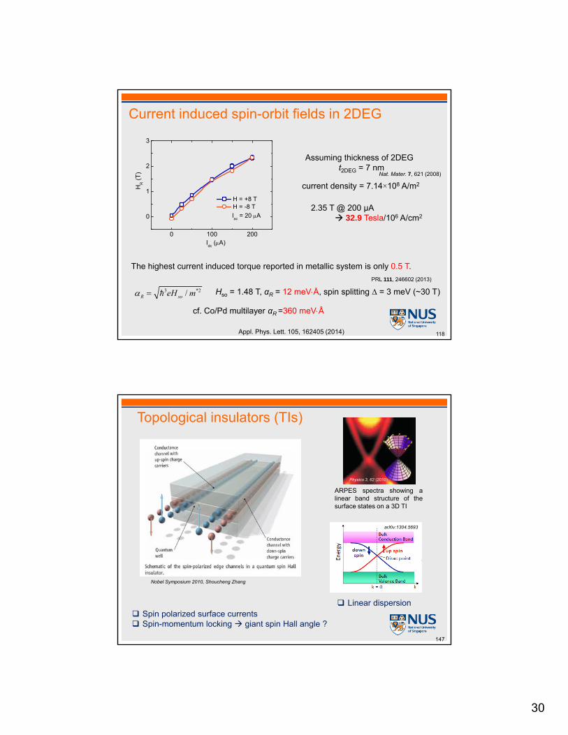
Current induced spin-orbit fields in 2DEG
Assuming thickness of 2DEG t2DEG = 7 nm
current density = 7.14×10⁸ A/m2
2.35 T @ 200 µA 32.9 Tesla/106 A/cm2
Nat. Mater. 7, 621 (2008)
0 100 200
0
1
2
3H
R (
T)
Idc
(A)
H = +8 T H = -8 T
Iac
= 20 A
The highest current induced torque reported in metallic system is only 0.5 T.
PRL 111, 246602 (2013)
3 *2/R soeH m Hso = 1.48 T, αR = 12 meVÅ, spin splitting ∆ = 3 meV (~30 T)
cf. Co/Pd multilayer αR =360 meVÅ
118Appl. Phys. Lett. 105, 162405 (2014)
Topological insulators (TIs)
arXiv:1304.5693
ARPES spectra showing alinear band structure of thesurface states on a 3D TI
Physics 3, 62 (2010)
Nobel Symposium 2010, Shoucheng Zhang
Spin polarized surface currents Spin-momentum locking giant spin Hall angle ?
Linear dispersion
147

31
BiSbTeSe2 topological insulators
148
10 100400
800
1200
1600
R
(
)
T (K)
BSTS
-120 -80 -40 02.0
2.5
3.0
After milling After (fit)
R (
k)
Gate voltage (V)
Before milling Before (fit)
2 K
Phys. Rev. B, 90, 235427 (2014)
BiSbTeSe2 is semiconducting Sample has become more heavily n-doped after ion milling
-Charged impurity density(nimp): 7 × 10¹² 1.33 × 10¹³/cm2
-Carrier concentration: 2.36 × 10¹³ /cm2 5.53 × 10¹³ /cm2
-Mobility (μe): 106 52 cm2/(Vs)
Can TI survive after etching process?
Ar ion milling effects
149
-6 -4 -2 0 2 4 6
-0.6
-0.4
-0.2
0.0
(e2 /h
)
H (T)
2K 10K 30K 40K 50K fit after milling
Phys. Rev. B, 90, 235427 (2014)
Negative MR originates from disorder
-8 -6 -4 -2 0 2 4 6 8
300
400
500
600
700
800
900
1000
R(o
hms)
Magentic Field(Tesla)
2K 5K 10K 20K 30K 40K 50K 60K 70K 80K 90K 100K
Linear
Parabolic
[BiSbTeSe (1.5‐0.5‐1.8‐1.2)]
Linear MR at LTParabolic MR at RT

32
Robustness of the topological surface states
150
0 20 40 60 80 100
-1.0
-0.5
0.0
T (K)
before milling after milling
0 20 40 60 80 1000
20
40
60
80
100 Before milling Before milling (Fit) After milling After milling (Fit)
L (n
m)
T (K)
L T -0.58 (before)
L T -0.56 (after)0 25 500
2
4
(x
10-7)
(-1T
-2)
T (K)
Phys. Rev. B, 90, 235427 (2014)
-A decay constant of -0.5 in L indicates two-dimensional (2D) electron-electron scattering for the sample before and after milling.-The behavior of surface states is unaffected by the introduction of disorder, as inferred from the similar values of α and the behavior of L.-Surface states are remarkably robust against external damage induced by ion milling.
Experimental setup
- Signal generator to excite magnetization dynamics in NiFe through a coplanar waveguide
- Voltmeter to measure spin pumping induced ISHE
- Vector network analyzer for FMR measurements
V
Magnetization oscillation provides high density spin currents into TI and a transverse voltage is detected in TI spin detector.
153Phys. Rev. B 90, 094403 (2014)

33
ISHE measurements
θsh = 0.01λsf = 6.2 nm
2 2 2 2 2
2 2 2 2
42tanh
28 4
r rf sfISHE BiSesh BiSe
BiSe sf
g h M MV dewd
R dM
157Phys. Rev. B 90, 094403 (2014)
0.0 0.2 0.4 0.6-2
0
2
4
6
8
10
3 GHz 4 GHz 5 GHz 6 GHz fitting
VIS
HE(
V)
B (kOe)
0 5 10 15 20 25 30 35 40
0.10
0.15
0.20
0.25
0.30
Data Fitting
VIS
HE/R
(V
/)
Bi2Se3 thickness (nm)
(c)
VISHE ~
R is resistance of the film
Js is induced spin current
θSH is spin Hall angle
SHsJR
Extracted spin Hall angle
• 1-2% of spin Hall angle is identified, which is already comparable to the best data from heavy metals (Pt, Ta).
• lso ~ λsf suggest that spin-orbit coupling is dominant source of spin scattering
-8 -4 0 4 8-0.06
-0.04
-0.02
0.00Data HLN fitting
G
(e
2 /h)
Magnetic field (T)0 50 100 150 200 250 300
0.8
1.2
1.6
2.0
2.4
Temperature (K)
sh (
%)
5
6
7
8
9
10
sf (
nm)
Spin orbit length, lso = 6.9 nm
161Phys. Rev. B 90, 094403 (2014)

34
No spin momentum locking
0 50 100 150 200 250 300
0.8
1.2
1.6
2.0
2.4
Surface (sh1)
Bulk (sh2)
sh
(%)
Temperature (K)
0 50 100 150 200 250 300
6
8
10
12
Temperature (K)
sf
(nm
)
(a) (b)
- Assumed spin Hall angle at opposite surfaces was taken to be of opposite signs.
- Spin Hall angle does not show any clear distinction between the surface and bulk value
- Momentum locking signature is not detected.
163Phys. Rev. B 90, 094403 (2014)
Comparison with other reports
Nature 511, 449 (2014) Nat. Mater. 13, 699 (2014)
Spin torque ferromagnetic resonance
measurements θSH = 2.0 – 3.5
Magnetization switching by current induced
spin orbit torque θSH = 140 – 425
In these experiments, a charge current flows through the TI material, unlike ours.
164

35
-1000 0 1000-4
-2
0
2
4
6 50 K 20 K
f = 8 GHz
300 K 200 K 100 K
V (V
)
H (Oe)
ST-FMR measurement of Bi2Se3/CoFeB
ST-FMR measurements with a lock-in amplifier at H = 35. ST-FMR signal (Vmix) can be fitted by a sum of symmetric and
antisymmetric Lorentzian functions:
mix s sym ext a asym ext( ) ( )V V F H V F H Vs: in-plane torque || on CFBVa: total out-of-plane torque
PRL 114, 257202 (2015) 167
In-plane spin-orbit torque ratio in Bi2Se3/CoFeB
0 50 100 150 200 250 3000.0
0.1
0.2
0.3
0.4 D 1 D 2 D 3
By Vs Only
D 1 D 2 D 3
T (K)
||
By Vs/V
a
|| (ǁ) increases steeply and nonlinearly to ~ 0.42 at low temperature and
could be almost 10 times larger than that at 300 K.
The polarization direction of || is consistent with spin-momentum-locked TSS.
|| by 1st and 2nd methods shows a significant difference below ~ 50 K, other
out-of-plane torque may contribution besides Oe.
170Wang et al., PRL 114, 257202 (2015)
1 10 100
200
300
400
T(K)
Rxx
(
)
Bi2Se
3 20 QL

36
0 50 100 150 200 250 300
0
1
2
3
T (K)
(Oe)
D 1 D 2 D 3
0 50 100 150 200 250 3000.0
0.1
0.2
0.3
0.4
T (K)
D 1 D 2 D 3
() also increases at low temperature similar to || (ǁ). Rashba-split state in 2DEG of Bi2Se3 is not the main mechanism for . Hexagonal warping in the TSS of Bi2Se3 can account for ().
Out-of-plane spin-orbit torque ratio in Bi2Se3/CoFeB
173Wang et al., PRL 114, 257202 (2015)
Out-of-plane torque in Bi2Se3
175
Wang et al., PRL 107, 207602 (2011)
Bi2Se3
Nomura et al., PRB 89, 045134 (2014)
-Recent reports showed there is substantial out-of-plane spin polarization due to
Hexagonal warping.
-Hexagonal warping in the TSS of Bi2Se3 can account for ().

37
Estimation of || from topological surface states (TSS)
0 50 100 150 200 250 300
0.6
0.9
1.2
0 50 100 150 200 250 3008
9
10
11
12
13
T (K)
n2
D (
10
13/c
m2 )
Bi2Se
3
I B
iSe/I C
FB
T (K)
By estimating ITSS:I2DEG:Ibulk, || from only TSS at low temperature is ~ 2.1 ±
0.39 (with bulk contribution) ~ 1.62 ± 0.18 (without bulk contribution)
2D TSS 2DEG bulk= 2 + 2 +n n n n d
178Wang et al., PRL 114, 257202 (2015)
kF-TSS ~ 0.14 – 0.17 Å-1
kF-2DEG ~ 0.1 – 0.12 Å-1
If we assume TSS thickness ~ 1 nm, the 2D spin orbit torque efficiency SOT ~ 0.8-1.05 nm. IREE ~ 0.2-0.33 nm in Ag/Bi interface [Nat. Commun. 4, 2944 (2013)]
nTSS ~ 1.56 − 2.3×1013 cm-2
n2DEG ~ 1.59 − 2.3×1013 cm-2
nbulk ~ 1 − 3.1×1019 cm-3
(~ 1 − 3.1×1013 cm-2)
kF-bulk ~ 0.066 – 0.097 Å-1
kF-bulk < kF-2DEG < kF-TSS and n2DEG < 2 nTSS
Exotic spin Hall angles from topological insulators
180
spin Hall angle (SH) = 2~3.5ST-FMR (Cornell)
Nature 511, 449 (2014)
PRB 90, 094403 (2014)
SH = 2 (low temp)ST-FMR (NUS)
SH = 140-425 (low temp)spin-orbit switching (UCLA)
Nat. Mater. 13, 699 (2014)
PRL 113, 196601 (2014)
SH = 0.01Spin-pumping (Tohoku)
SH = 0.01Spin-pumping (NUS)
PRL 114, 257202 (2015)
SH = 0.01-0.4Spin-pumping (Minnesota)
Nano Lett 15, 7126 (2015)

38
181
Coexistence of surface states and Rashba bands
Surface vs. bulk contribution to spin Hall angle ?
Nat. Comm. 3,1159 (2012)
198
(b)
(a)
y
x
Normal incidence
ObjectiveLens 100x
sample
BS1
BS2
λ/2
PEM
GT
Chopper
Photodiode
xyz stage
Lock-in amplifier
Chopper/PEM controller
ReferenceSignal
(c)
yj
x
y
z
iθ
iφ
i iθ = 45 φ 0
i iθ = 0 φ 0
Oblique incidence
Spin dependent photocurrents in Bi2Se3
Besbas et al., Adv. Opt. Mat. (in‐press 2016)

39
199
4 8 12 16 20
4
8
12
16
20
position (m)
posi
tion
(m
)
-20.0
-10.0
0.0
10.0
20.0
HDP (V)
Electrode 2
Bi2Se3
Experiment condition:Circularly polarized light normal incidence on TI. Bias current is zero.
Observation:The photocurrent generation at TI-metal interface.
Analysis:1. The observed signal at the interface is due to electrostatic potential
and hexagonal warping effect.2. The smaller observed signal on TI is due to defected induced
electrostatic potential.
4 8 12 16 20
4
8
12
16
20
position (m)
posi
tion
(m
)
-20.0
-10.0
0.0
10.0
20.0
photovoltage (V)
Electrode 1
Bi2Se3
Besbas et al., Adv. Opt. Mat. (in‐press 2016)
0.0 0.2 0.40
1
2
3
4
W
Ta
W
Pt
Ta
Pt
Sp
in o
rbit
to
rqu
e
(kO
e pe
r 10
8 A/c
m2 )
Pd
30
20
10
0
Sw
itch
ing
cu
rre
nt
den
sity
(MA
/cm
2 )
SH
BiSbTe (UCLA)
BiSbTe (UCLA)8.9E4 A/cm2
Co/Pd (NUS)
LAO/STO (NUS)
θSH
5 kOe
480~1460 T
3000 T
4.4 140
Bi2Se3 (Cornell, NUS)
=2
2
200

40
Open questions
• What is beyond band structures in Dirac/Weyl field?
• Can we make useful devices?
• Then what properties do we need to utilize?
– Spintronics – spin momentum locking
– Optoelectronics (THz) – intraband transition
237
Dr. Xuepeng Qiu Dr. Yang Wu
Antonio Castro Neto (NUS)
Andre Geim (Manchster)
T. Venkatesan (NUS)
Seah Oh (Rutgers)
Aurelien Manchon (KAUST)
Lan Wang (RMIT Univ.)
K-J. Lee (Korea Univ.)
Dr. K. NarayanapillaiDr. Yi Wang Dr. Jean Besbas Dr. Qisheng Wang
238
Related Documents


![Strain and the optoelectronic properties of non-planar ... · D crystalline soft materials that acquire topological defects while conforming to non-planar shapes [12-15], the materials](https://static.cupdf.com/doc/110x72/5b82c1247f8b9a934f8bb20e/strain-and-the-optoelectronic-properties-of-non-planar-d-crystalline-soft.jpg)