Louisiana State University LSU Digital Commons LSU Doctoral Dissertations Graduate School 2014 Spin-Mediated Transport in Superconducting and Spin-Polarized Systems Joseph C. Prestigiacomo Louisiana State University and Agricultural and Mechanical College Follow this and additional works at: hps://digitalcommons.lsu.edu/gradschool_dissertations Part of the Physical Sciences and Mathematics Commons is Dissertation is brought to you for free and open access by the Graduate School at LSU Digital Commons. It has been accepted for inclusion in LSU Doctoral Dissertations by an authorized graduate school editor of LSU Digital Commons. For more information, please contact[email protected]. Recommended Citation Prestigiacomo, Joseph C., "Spin-Mediated Transport in Superconducting and Spin-Polarized Systems" (2014). LSU Doctoral Dissertations. 1114. hps://digitalcommons.lsu.edu/gradschool_dissertations/1114

Welcome message from author
This document is posted to help you gain knowledge. Please leave a comment to let me know what you think about it! Share it to your friends and learn new things together.
Transcript
Louisiana State UniversityLSU Digital Commons
LSU Doctoral Dissertations Graduate School
2014
Spin-Mediated Transport in Superconducting andSpin-Polarized SystemsJoseph C. PrestigiacomoLouisiana State University and Agricultural and Mechanical College
Follow this and additional works at: https://digitalcommons.lsu.edu/gradschool_dissertations
Part of the Physical Sciences and Mathematics Commons
This Dissertation is brought to you for free and open access by the Graduate School at LSU Digital Commons. It has been accepted for inclusion inLSU Doctoral Dissertations by an authorized graduate school editor of LSU Digital Commons. For more information, please [email protected].
Recommended CitationPrestigiacomo, Joseph C., "Spin-Mediated Transport in Superconducting and Spin-Polarized Systems" (2014). LSU DoctoralDissertations. 1114.https://digitalcommons.lsu.edu/gradschool_dissertations/1114

SPIN-MEDIATED TRANSPORT IN SUPERCONDUCTING AND SPIN-POLARIZED SYSTEMS
A Dissertation
Submitted to the Graduate Faculty of the Louisiana State University and
Agricultural and Mechanical College in partial fulfillment of the
requirements for the degree of Doctor of Philosophy
in
The Department of Physics and Astronomy
by Joseph C. Prestigiacomo
B.S., Louisiana State University, 2009 December 2014

ii
ACKNOWLEDGMENTS
Over the past ten years as a student at Louisiana State University, I have had the privilege
of working with a number of people to whom I owe a great deal of gratitude. First, I would like
to thank my professor Dr. Phil Adams. Since my time as an undergrad, he has not only mentored
me in his own fields of study but has also given me the academic freedom to explore many other
areas of science, helping me to grow into the researcher that I am today. I also greatly appreciate
his funding my trips to scientific conferences, which helped me to develop crucial networking
skills. His former post-doc Yimin “Max” Xiong deserves a thanks as well, for his part in my
orientation to the capabilities of Dr. Adams’ laboratory, as well as a thanks to his late post-doc
Tijiang “TJ” Liu, for his assistance in running day-to-day operations in the lab.
Another person that I owe many thanks to is Dr. Shane Stadler, who worked with me one
on one to ensure I was adept at all of the aspects of his lab and offered me side projects that would
lead to my inclusion in a number of publications. I would also like to thank Profs. David Young
and John DiTusa for allowing me to participate in their projects and giving me access to their
equipment, which gave me invaluable research experience and directly contributed to this
dissertation. Thanks also go to Profs. Daniel Sheehy, Hwang Lee, and Les Butler for agreeing to
serve on my graduate committee.
Prof. Julia Chan and her students in the Chemistry department are owed a debt of gratitude
for their fruitful collaborative efforts that expanded my knowledge and understanding as a
scientist. Most notably, Devin Schmitt deserves special thanks for the many months he spent
working with me to discover a novel field-pulse memory effect in certain rare-earth based
intermetallic compounds.
iii
I would also like to thank the office staff members of the Physics and Astronomy
department. Arnell Nelson - for ensuring my graduate milestones were met, Ophelia Dudley -
for expediting financial protocols so that I was always reimbursed for conferences in a timely
manner, and to the entire machine shop staff – for lending me their expertise on many projects
that I undertook here at LSU.
Finally, I thank my wife and best friend, Brianna, for supporting me throughout my
undergraduate and graduate career, for the sacrifices she made when I needed to focus on work
the most, and for her unwavering faith in my success, even in times of my greatest self-doubt.

iv
TABLE OF CONTENTS
Acknowledgments ……………………………………………………………………..………… ii
Abstract ……………………………………………………………………………………….......v
Chapter 1. Introduction ………………………………………………………..……………..........1 2. Hall Effect and the Magnetotransport Properties of Co2MnSi1-xAlx Heusler Alloys....12 3. Asymmetric Avalanches in the Condensate of a Zeeman-limited Superconductor......28 4. Conclusions ..................................................................................................................48
Appendix
A1. Heusler Alloy-based Giant Magneto-impedance Effect Field Sensor: A Proposal to the National Research Council...................................................................................50
A2. Consent Policy............................................................................................................61
Vita ...............................................................................................................................................63

v
ABSTRACT
The effects of spin-imbalance on the electronic transport properties of spin-polarized and
superconducting systems have been studied in detail. The transport properties of the quaternary
Heusler alloys Co2MnSi1-xAlx (0 1), which have been theoretically predicted to develop a
half-metallic band structure as → 0, were investigated. Resistivity versus temperature
measurements as a function of Al concentration ( ) revealed a systematic reduction in the residual
resistivity ratio as well as a transition from weakly-localized to half-metallic conduction as → 0.
From measurements of the ordinary and anomalous Hall effects, the charge carrier concentration
was found to increase, while the anomalous Hall coefficient decreased by nearly an order of
magnitude with each sample as → 0 (∆ 0.25). Scaling of the anomalous Hall effect with
longitudinal resistivity reveals that both the skew-scattering and intrinsic contributions grow
quickly as → 1, indicating that disorder and band-structure effects cause the large anomalous
Hall effect magnitudes observed for Co2MnAl.
The non-equilibrium behavior of disordered superconducting Al films in high Zeeman
fields has also been investigated. The tunneling density-of-states of the films were measured
through the first-order Zeeman critical field transition. It is found that films with sheet resistances
of a few hundred ohms exhibit large avalanche-like collapses of the condensate on the super-
heating branch of the critical field hysteresis loop. In contrast, the transition back into the
superconducting phase (i.e., along the super-cooling branch) is always continuous. These
avalanches are suppressed by tilting the field as little as 1.5° and disappear above T = 300 mK,
although the transition remains hysteretic. The fact that the condensate follows an unstable
trajectory to the normal state suggests that the order-parameter in the hysteretic regime is not
homogeneous. It is argued that this unusual behavior is a manifestation of the disordered Larkin-

vi
Ovchinnikov phase, which is a disordered remnant of the elusive, spin-imbalanced
superconducting state known as the Fulde-Ferrell-Larkin-Ovchinnikov phase.

1
CHAPTER 1. INTRODUCTION
Spin-polarized systems constitute a diverse set of materials. In general, however, they all
share three key features. First, and foremost, is the phenomenon of electron spin-imbalance.
Though its origin varies from one material to the next, in all cases, it is associated with an
inequality in the density of states (DOS) for spin-up and spin-down electrons at the Fermi energy
(EF). Thus, their charge-carrier density (n) is primarily composed of either majority spin-up (n↑)
or spin-down (n↓) electrons. Secondly, they all exhibit some type of spin ordering, the origin of
which also varies between classes of materials. Despite those assorted roots, however, their
particular form of magnetism is often uniquely associated with the underlying mechanism of
their spin-imbalance. Lastly, their magnetization direction determines the spatial orientation of
their majority-spin electrons. All together, these features make them useful electrode materials
for thin-film devices that take advantage of spin-polarized tunneling, such as magnetic tunnel
junctions (MTJs) [1], or of other spin-dependent scattering processes (e.g. giant magneto-
resistance sensors) [2-4]. Indeed, by combining these extraordinary materials with recent
advancements in nanofabrication technology, a new class of electronics device has emerged, one
that utilizes the conduction electron’s charge and spin degrees of freedom; these are known as
spintronic devices [5].
An overarching goal of the work presented herein is to contribute to the general
understanding of spin-imbalance, with an effort to either improve the performance of or discover
new materials that are well suited for spintronics applications. A spintronic material’s
performance is mainly determined by the value of its spin-polarization at the Fermi energy (P), a
ratio that quantifies the level of spin-imbalance in the system. P is defined as P = | n↑ - n↓| / (n↑ +
n↓), so that its value ranges between 0 and 1, corresponding to a material with no spin-
polarization (e.g. most paramagnetic metals) and to a material with full spin-polarization (100%
2
of the electrons are spin-up or -down), respectively. To illustrate how this parameter influences
performance, we can use Julliere’s formula for the tunneling magneto-resistance (TMR) ratio of
a MTJ [1], given by ΔTMR = 2P1P2 / (1 - P1P2), where P1 and P2 are the spin-polarizations of the
junction’s electrodes. According to this equation, the ΔTMR approaches infinity when P1 = P2
→ 1, validating the notion that materials with high spin-polarization are the best candidates for
spintronics applications. Until recently, the electronics industry used ordinary ferromagnetic
materials (i.e. iron, nickel, and cobalt, or alloys thereof) for their spin-polarized current sources,
but despite their adequate performance in numerous devices, such as the GMR-based read-heads
in modern hard-disk drives, their moderate spin-polarization values (P ~ 0.4) [6] have prevented
spin-based electronic technologies from reaching their full potential.
At the forefront of the new, potentially superior spintronics-materials are the half-metallic
ferromagnets (HMF). The term half-metallic refers to the character of their spin-imbalance, n↓ =
0. Since their prediction in the early 1980s [7], several classes of compounds have emerged
which were thought to be HMFs, including the pyrite [8] and spinel [9] sulfides, a few double-
perovskites [10, 11], the transition-metal oxides magnetite [12] and chromium dioxide [13], the
colossal-magnetoresistance materials [14], and a multitude of Heusler alloys [15]. Of primary
concern when selecting a HMF for spintronics-duty is the temperature dependence of P. In this
regard, the cobalt-based full Heusler alloys are considered the material of choice [16], for their
high Curie temperatures, relatively wide minority-spin band gaps, and high order-disorder (L21
to B2) transformation temperatures that enable them to be easily synthesized with negligible
structural defects. Moreover, they offer an exciting opportunity to optimize half-metallic
character through chemical doping [17]. Recent band-structure calculations of several Co-based
Heusler systems have revealed that an effective shift of EF, in an otherwise unaltered DOS, is

3
possible under certain chemical substitutions. Not only is this valuable from an applications
standpoint but from a fundamental one as well.
Although many doping studies have been carried out on Heusler alloys in the past, very
few, if any, experiments have been performed on the magneto-transport properties of Heuslers
showing this type of behavior. This is unfortunate because, in principle, magneto-transport
measurements can function as a probe of the spin-dependent scattering mechanisms that are
modified as the spin-imbalance is adjusted. In addition, the complex interplay between half-
metallicity and magnetism can be explored systematically, and without significant disruption of
the overall properties that define the system. The work in the Chapter 2 was performed with
these issues in mind. I have explored the structural, magnetic, and electrical transport properties
of such a Heusler system, Co2MnSi1-xAlx, focusing particularly on the changes to the magneto-
transport properties that are concomitant with variations of the spin-polarization, hypothetically
induced as EF is tuned by doping.
The relative spin-imbalance level can be inferred from such a study but there is
nevertheless a great demand in the half-metallic community for direct measurements of P. In
particular, it is crucial that a given spin-resolved probe extracts the spin-polarization at the Fermi
energy, not at other energy scales, because EF is where electrical transport occurs. Clearly, to do
this accurately, a spin-resolved probe with a high resolution is required. There are, in fact,
several of these: point-contact Andreév reflection [6], spin-resolved photoemission spectroscopy
[18], MTJs (inverting Julliere’s formula), etc.; however, the highest resolution technique is the
planar-tunneling spin-resolved DOS strategy pioneered by Tedrow and Meservey [19]. This
technique uses the spin-singlet character of a superconductor (SC) in a high Zeeman-field as a
probe of the spin-states in other materials. As the strength of the field increases so does the spin-
resolution of the probe, until the Zeeman-limited critical-field transition occurs near the

4
Clogston-Chandrasekhar value [20, 21] ∆ / √2, where ∆ is the width of the SC gap in
the DOS.
Interestingly, many anomalous spin-mediated effects appear in this superconducting
regime, where the SC naturally provides the spin-resolved DOS. These effects include slow,
stretched-exponential relaxations and avalanches in the magneto-transport properties, classic
indicators of non-equilibrium dynamics [22]. The origin of this behavior is still a matter of
debate [23, 24], and though these instabilities can potentially disrupt a measurement of P, they
have deep implications as to the nature of the superconducting order parameter in the regime
where the Zeeman splitting is of the order of the superconducting gap energy. Therefore, we
move to study the underlying physics that forms the basis of this technique.
A conventional, BCS-type superconductor achieves its zero-resistance state below a
critical temperature, Tc, via a phonon-mediated, attractive, interaction between pairs of electrons
with opposite spin-angular momentum [25]. This binds the two electrons into a spin-singlet,
bosonic quasiparticle called a Cooper pair. The condensation of these Cooper pairs into a
superconducting ground state is reflected in the single-particle (quasi-particle) DOS as an energy
gap, Eg = 2∆ , centered at EF. Furthermore, since many Cooper pairs comprise the SC
condensate, it behaves in a collective manner as a single, macroscopic quantum state whose
order-parameter has an amplitude and a phase.
A SC is usually characterized by the response of its condensate to an applied magnetic
field. In a bulk SC, a weak magnetic field cannot penetrate the interior except for a thin layer at
the surface; this is known as the Meissner effect. At stronger fields, the pure Meissner response
breaks down, and the manner in which this occurs is the basis of categorizing all SCs as type I or
type II. If, however, the SC is a film of thickness d, oriented with the field parallel to the plane,
the critical field due to the Cooper pairs’ orbital response varies as d-3/2 and it is a 2nd-order phase

5
transition [26]. Once d < the coherence length ξ (an effective “size” of the Cooper pairs), this
critical field will be pushed to extremely high values so that Zeeman splitting precedes orbital
depairing as the mechanism for the SC-N state transition. Thus, the Zeeman splitting of the
Cooper pairs’ spin-up/spin-down electrons (Ez = gμBH||) determines the critical field magnitude.
This occurs when Ez is of the order of ∆ (Hc|| ~∆ / √2). Clogston and Chandrasekhar further
showed that this Zeeman-limited transition becomes a 1st-order transition below a tricritical
temperature (Ttri), provided the film possesses very low intrinsic-spin orbit scattering.
The field of superconducting tunneling spectroscopy began experimentally with a Nobel
Prize winning discovery made by Ivar Giaever at the General Electric Research Laboratory in
1960 [27]. By cooling Al/Al2O3/Pb thin film sandwiches to T = 1.6 K (thereby placing the films
in the N/I/SC state), applying a voltage (V) to the outer layers, and then measuring the tunneling
current (I) between them, the derivative dI/dV of the I(V) curves yielded the Bardeen-Cooper-
Schrieffer (BCS) superconducting DOS for quasiparticle excitations. Theoretically, this is
because at low temperatures and low voltages (~µV-mV range), the differential tunneling-
conductance (G) is proportional to the product of the DOS of the junction’s electrode and the
DOS of the counter-electrode (CE). The DOS is nearly constant for most ordinary metals at
meV energy scales, resulting in a flat tunneling-spectrum. However, the DOS varies drastically
within a few meV of EF for a superconductor, so that its electronic structure dominates G. Not
only did this technique provide the first direct evidence of an energy gap in the DOS of a
superconductor, it revealed that, in zero magnetic field, the states formerly within this gap are
collected and relocated into two sharp singularities at the gap’s edges. These are known as BCS
coherence peaks.
Building on Giaever’s work, in the early 1970’s, Tedrow and Meservey adapted the
planar-tunneling technique to function as a probe of the counter-electrode’s spin-state [19]. A

6
simple yet essential change was made to the original design; they replaced the SC electrode’s
relatively thick lead film with an ultra-thin (d < ξ) aluminum film. Al was chosen because it
exhibits low spin-orbit scattering, meaning its Cooper pairs represent true spin-singlet
wavefunctions. Hence, a magnetic field applied parallel to the plane of the junction causes a
sizeable Zeeman splitting of the coherence peaks, transforming each of them into two highly
resolvable spin-bands, thus providing separate tunneling channels for up- and down-spin
electrons (see Figure 1-1). Accordingly, if the CE is an ordinary (i.e. paramagnetic) metal, the
peak heights of the spin-up and -down bands are equal; however, if a spin-imbalanced material is
used, then the difference in its spin-species populations is reflected in the relative heights of the
respective tunneling-conductance peaks. Thus, the spin-singlet character of thin Al films gives
one a spin-resolved tunneling probe.
Figure 1-1: Tunneling conductance as a function of voltage for an aluminum film (d < ξ) in a parallel field, revealing the energy gap at V = 0 and the symmetric Zeeman splitting of the superconducting DOS spectrum. The red arrows denote the spin assignment of each BCS coherence peak.

7
While planar-tunneling spectroscopy has become an indispensable tool for measuring the
P of spin-imbalanced systems, it can also serve as a versatile probe of the Zeeman-limited SC
condensate itself. For instance, a hysteresis loop associated with the 1st-order Zeeman-limited
critical-field transition was not directly observed until 1994 [28], 32 years after its first
prediction, via transport measurements on electro-chemically anodized Al films. Despite this
breakthrough, however, it was not confirmed that the hysteresis was intrinsic to the SC
condensate until 1999, when tunneling experiments on high-quality quench-condensed Al films
were performed [29]. Likewise, it has never been confirmed whether the non-equilibrium
dynamics of the transport at the Zeeman-limited transition are an intrinsic feature of the
condensate.
Indeed, very little is known about the physics of a superconductor in a state of dynamical
spin-imbalance upon entering the non-equilibrium region of a 1st-order phase transition.
Therefore, in Chapter 3, I describe a series of experiments on the electrical transport and
tunneling properties of superconducting Al films and Al/Al2O3/Al planar tunnel-junctions near
the Zeeman-limited critical field transition as a function of time, temperature, field sweep-rate,
field step-size, field orientation, and sheet resistance. In particular, the time and field step-size
dependence measurements are taken in high-resolution, to reveal hidden dynamics that can be
occluded by coarsely spaced data points. I will interpret the results of this study in the context of
the disordered-Larkin-Ovchinnikov phase, which is a disordered remnant of the elusive, spin-
imbalanced superconducting state known as the Fulde-Ferrell-Larkin-Ovchinnikov (FFLO)
phase.
The FFLO phase is a novel SC state believed to emerge between the low- and high-field
phases of the 1st-order Zeeman-limited critical field transition, and was predicted in the late
1960’s. In this intermediate phase, the pairing amplitude (Δ) is spatially modulated, resulting in

8
polarized normal-state regions coexisting with spatially isolated superconducting domains (see
Figure 1-2). Experimental evidence of FFLO SC is rare [30-32], despite the development of
analytical techniques to identify it [33]. Recently, however, the over 40-year mystery of the
excess zero-bias tunneling-conductance 0V near the Zeeman critical field of thin Al films
was quite convincingly explained by Loh et al in their justification for the existence of a
disordered Larkin-Ovchinnikov (d-LO) state [34]. Compared to conventional FFLO SC, the d-
LO state is much more robust. Their simulations showed that Δ actually conforms to the
homogenously disordered landscape by supporting Andreév bound-states within the SC domains
(a) BCS Superconducting State
(c) Normal State
(b) FFLO State
Figure 1-2. The transition of the pairing amplitude (y-axis) versus spatial dimension (x-axis) as a function of increasing Zeeman field. (a) In the BCS state, Δ is spatially homogenous with long-range coherence. (b) In the FFLO state, Δ can take positive and negative values; these are superconducting regions. The point where Δ crosses zero is a normal state region. (c) In the normal state, Δ is zero and the conduction electrons are spin-polarized.
Increasing Zeem
an Field

9
(see Figure 1-3). These bound states lie at low energy and manifest in the superheating curve of
the tunneling hysteresis loop as a slow, continuous increase of 0V towards the normal state.
This is in disagreement with the BCS theory, which predicts that the Zeeman-limited transition
occurs suddenly, as a sharp, discontinuous transition. In addition, if one examines the hysteresis
loops of the tunnel conductance carefully, the excess conductivity can be seen to be located
where the avalanches occur, strongly suggesting that they are related to the d-LO state.
Figure 1-3. (a) Combined spatial map of the pairing amplitude Δ(r) and the magnetization m(r) of a homogenously disordered, BCS superconductor, in a magnetic field just below the Zeeman critical field transition. Red (blue) regions correspond to large positive (negative) Δ(r), brown regions are where m is large, and white regions represent empty sites or localized pairs that do not contribute to SC or to magnetism. (b) and (c) show the oscillation of Δ along the vertical dashed line of (a) [34].
10
This introduction was intended to provide historical and scientific context to the research
presented in the following chapters. There, a more technical description of the research
methodologies and discoveries that were revealed can be found.
1.1 References
[1] M. Julliere, Phys. Lett. A 54, 225 (1975).
[2] M. Johnson and R. H. Silsbee, Phys. Rev. Lett. 55, 1790 (1985).
[3] M. N. Baibich, J. M. Broto, A. Fert, F. N. Van Dau, F. Petroff, P. Etienne, G. Creuzet, A. Friederich, and J. Chazelas, Phys. Rev. Lett. 61, 2472 (1988).
[4] G. Binasch, P. Grünberg, F. Saurenbach, and W. Zinn, Phys. Rev. B 39, 4828 (1989).
[5] C. Chappert, A. Fert, and F. N. Van Dau, Nat. Mater. 6, 813 (2007).
[6] R. J. Soulen et al., Science 282, 85 (1998).
[7] R. A. de Groot, F. M. Mueller, P. G. v. Engen, and K. H. J. Buschow, Phys. Rev. Lett. 50, 2024 (1983).
[8] G. L. Zhao, J. Callaway, and M. Hayashibara, Phys. Rev. B 48, 15781 (1993).
[9] V. N. Antonov, V. P. Antropov, B. N. Harmon, A. N. Yaresko, and A. Y. Perlov, Phys. Rev. B 59, 14552 (1999).
[10] K. I. Kobayashi, T. Kimura, H. Sawada, K. Terakura, and Y. Tokura, Nature 395, 677 (1998).
[11] K. I. Kobayashi, T. Kimura, Y. Tomioka, H. Sawada, K. Terakura, and Y. Tokura, Phys. Rev. B 59, 11159 (1999).
[12] A. Yanase and K. Siratori, J. Phys. Soc. Jpn. 53 (1984).
[13] K. Schwarz, J. Phys. F: Met. Phys. 16, L211 (1986).
[14] W. E. Pickett and D. J. Singh, Phys. Rev. B 53, 1146 (1996).
[15] M. I. Katsnelson, V. Y. Irkhin, L. Chioncel, A. I. Lichtenstein, and R. A. de Groot, Rev. Mod. Phys. 80, 315 (2008).
[16] T. Simon, G. Oksana, H. Jaroslav, and H. Burkard, J. Phys. D: Appl. Phys. 43, 193001 (2010).
[17] K. Ozdogan, E. Sasioglu, and I. Galanakis, J. App. Phys. 103, 023503 (2008).
11
[18] D. J. Peter, Rep. Prog. Phys. 60, 1217 (1997).
[19] P. M. Tedrow and R. Meservey, Phys. Rev. Lett. 26, 192 (1971).
[20] B. S. Chandrasekhar, App. Phys. Lett. 1, 7 (1962).
[21] A. M. Clogston, Phys. Rev. Lett. 9, 266 (1962).
[22] W. H. Wu and P. W. Adams, Phys. Rev. Lett. 75, 772 (1995).
[23] F. Zhou and B. Spivak, Phys. Rev. Lett. 80, 5647 (1998).
[24] E. Bielejec and W. Wu, Phys. Rev. Lett. 87, 256601 (2001).
[25] J. Bardeen, L. N. Cooper, and J. R. Schrieffer, Phys. Rev. 106, 162 (1957).
[26] P. G. d. Gennes and M. Tinkham, Physics 1, 107 (1964).
[27] I. Giaever, Phys. Rev. Lett. 5, 147 (1960).
[28] W. H. Wu and P. W. Adams, Phys. Rev. Lett. 73, 1412 (1994).
[29] V. Y. Butko, P. W. Adams, and E. I. Meletis, Phys. Rev. Lett. 83, 3725 (1999).
[30] F. Wu, G.-C. Guo, W. Zhang, and W. Yi, Physical Review Letters 110, 110401 (2013).
[31] B. Bergk, A. Demuer, I. Sheikin, Y. Wang, J. Wosnitza, Y. Nakazawa, and R. Lortz, Phys. Rev. B 83, 064506 (2011).
[32] A. Bianchi, R. Movshovich, C. Capan, P. G. Pagliuso, and J. L. Sarrao, Physical Review Letters 91, 187004 (2003).
[33] A. I. Buzdin, Reviews of Modern Physics 77, 935 (2005).
[34] Y. L. Loh, N. Trivedi, Y. M. Xiong, P. W. Adams, and G. Catelani, Physical Review Letters 107, 067003 (2011).

12
CHAPTER 2.† HALL EFFECT AND THE MAGNETOTRANSPORT PROPERTIES OF Co2MnSi1-xAlx HEUSLER ALLOYS
2.1 Introduction
The quinternary full-Heusler compound Co2(Cr1-yMny)(Si1-xAlx) with the L21 crystal
structure (see Figure 2-1) has proved to be a useful system to investigate the optimization of half-
metallic behavior through doping [1]. It has been shown using the coherent potential
approximation, the virtual crystal approximation, and by supercell calculations that the electronic,
magnetic, and gap-related properties of this intermetallic can be tuned by changing the relative
concentrations of the low-valent transition metal and sp atoms. A particularly interesting subset
of this class of compounds is obtained with 1 and a variable Al concentration ( ), Co2MnSi1-
xAlx. Theoretically, it is expected that, as x increases from 0 to 1, the Fermi energy ( ) will shift
within the minority spin band from the center of a relatively wide gap (~0.6 eV) to the upper edge
of the valence band. Recently, this shift was observed in the tunneling conductance (G-V)
measurements of magnetic tunnel junctions (MTJs) composed of B2-ordered epitaxial films
having different Al concentrations (x) [2]. Several desirable properties are found in the full-
stoichiometric compounds. Co2MnSi ( 0) is well known for its potential use in spintronic
applications. It has an extremely high Curie temperature of ~1000 K [3, 4], and produces giant
tunnel magnetoresistance ratios (TMR) when used as an electrode in magnetic tunnel junctions
(MTJ) [5]. The compound Co2MnAl ( 1) has not been predicted to be fully spin-polarized,
however its high Curie temperature of ~700 K [3, 6], combined with its large anomalous Hall
effect (AHE) [7], have redeemed it as a valuable material for Hall effect sensors in automotive
applications [8].
†Reprinted with permission from Prestigiacomo, J. C.; Young, D. P.; Adams, P. W.; Stadler, S., J. App. Phys. 115, 043712 (2014). Copyright 2014, AIP Publishing LLC.

13
In light of the above-mentioned potential applications of the full-stoichiometric
compounds, it is worthwhile to investigate the physical properties of Co2MnSi1-xAlx as a function
of Al content. The dependence of the magnetic and structural properties of Co2MnSi1-xAlx on Al
content have been previously investigated [3, 9, 10]. Notably, in Reference 3, it was shown that
the bulk polycrystalline series follows the Slater-Pauling rule, as predicted by the theory of spin-
polarization in Heusler alloys [11]. This rule relates the total number of valence electrons in a unit
Figure 2-1. Schematic representation of the L21 structure for a full-Heusler alloy X2YZ. The lattice is composed of four interpenetrating face-centered-cubic sublattices: two by X, one by Y, and one by Z. The unit cell is a face-centered-cubic lattice with a basis of four atoms at Wyckoff
positions: X at (0, 0, 0) and at ( , , ), Y at ( , , ), and Z at ( , , ). Anti-site disorder due to
the random occupation of the Y and Z atomic sites results in the B2 structure, while random occupation of the X, Y, and Z atomic sites results in the A2 structure.

14
cell to the total saturation magnetization in units of Bohr magnetons per formula unit, meaning
that the magnetization can be precisely controlled by tuning the value of .
Since Co2MnSi1-xAlx is predicted to have spin-polarized charge carriers, carrier-dependent
magnetotransport measurements should provide insight into interesting electrical conduction
properties when the Fermi level is systematically shifted through majority/minority bands by
doping. A particularly revealing phenomenon, and therefore an important tool, is the Hall effect,
whose ordinary and anomalous contributions contain terms sensitive to the details of the Fermi
surface [12, 13]. Indeed, it has been theoretically shown that Co2MnAl may exhibit a fully spin-
polarized Hall current despite its only partially spin-polarized band structure [14]. Therefore, this
study includes measurements of the magnetoresistance (MR) and the Hall resistivity of bulk
polycrystalline Co2MnSi1-xAlx ( 0, 0.25, 0.5, 0.75, and 1) as a function of temperature and
applied magnetic field. Interestingly, an applied field did not generate a detectable Hall voltage in
Co2MnSi (x = 0). Moreover, negligible field response was observed in the MR for all x, other than
the small artifacts leaked in by the Hall effect due to slight lead misalignments. The absence of
MR in Co2MnSi is consistent with previous observations in single-crystals [15], and probably
indicates negligible spin-disorder scattering. Nevertheless, a giant magneto-impedance effect was
observed for Co2MnSi that can be used for sensitive magnetic field detection. This effect is
discussed in more detail in Appendix A1.
2.2 Experimental Details
Bulk Co2MnSi1-xAlx (x = 0, 0.25, 0.5, 0.75, and 1) samples were synthesized by rf-induction
melting in a 4N purity Ar atmosphere. The polycrystalline samples were annealed at 1100 for
3 days and then at 600 for an additional 5 days. X-ray powder diffraction was used to confirm
that the L21 phase was obtained in all samples and that there were no impurity phases (see Figure
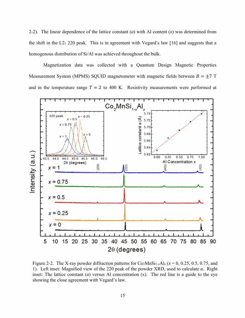
15
2-2). The linear dependence of the lattice constant (a) with Al content (x) was determined from
the shift in the L21 220 peak. This is in agreement with Vegard’s law [16] and suggests that a
homogenous distribution of Si/Al was achieved throughout the bulk.
Magnetization data was collected with a Quantum Design Magnetic Properties
Measurement System (MPMS) SQUID magnetometer with magnetic fields between 7 T
and in the temperature range 2 to 400 K. Resistivity measurements were performed at
Figure 2-2. The X-ray powder diffraction patterns for Co2MnSi1-xAlx (x = 0, 0.25, 0.5, 0.75, and 1). Left inset: Magnified view of the 220 peak of the powder XRD, used to calculate a. Right inset: The lattice constant (a) versus Al concentration (x). The red line is a guide to the eye showing the close agreement with Vegard’s law.
16
temperatures between 2 and 400 K in applied magnetic fields between ±9 T using a standard four-
wire technique with a QD PPMS equipped with the AC transport option. Sample cuts of
approximately 2.5 x 1.5 x 0.4 mm3 were taken from the interior of the ingots, polished, and then
sonicated in acetone for 1 hr before attaching 2 mil Pt leads with EPOTEK silver epoxy. Excitation
currents used were typically 10 mA with a measurement frequency of 31 Hz.
2.3 Results and Discussion
2.3.1 Temperature Dependent Resistivity
Resistivity versus temperature curves for Co2MnSi1-xAlx measured in zero field and
normalized by their values at 2 K are shown in Figure 2-3. The most obvious feature is the
remarkably high residual resistivity ratio (RRR) of ~4.5 for Co2MnSi, in sharp contrast to the
others in the series which display a relatively small, systematically decreasing RRR with
increasing Al content. In fact, the measured residual resistivity of ~3 µΩ-cm for the
polycrystalline Co2MnSi compares well with reported values for single crystal boules (~2.5 µΩ-
cm) [17, 18] and epitaxial films (~15 µΩ-cm) [19, 20]. A high RRR value and µΩ-cm-range
resistivity signifies a low level of temperature independent scattering due to sources such as
dislocations, impurities, or grain boundaries. Doping naturally introduces disorder; however, it is
not believed that this has induced significant formation of the A2 phase. If this were the case, we
would not expect to see such a close agreement with the Slater-Pauling rule or Vegard’s law.
Nonetheless, Heuslers containing Al are known to possess a higher degree of anti-site disorder
due to an exchange of atoms on the Mn-Al sites (B2 structure) [6, 21]. This is due to the fact that
their order-disorder (L21-B2) phase transition temperature ( ) decreases monotonically
with increasing Al content (~ 670 1300 ) [3]. In order to guarantee a pure L21 phase sample,
one must anneal it at ≪ . Samples that require a lower (i.e. those containing
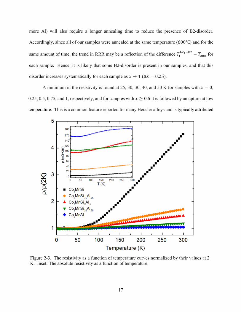
17
more Al) will also require a longer annealing time to reduce the presence of B2-disorder.
Accordingly, since all of our samples were annealed at the same temperature (600 ) and for the
same amount of time, the trend in RRR may be a reflection of the difference for
each sample. Hence, it is likely that some B2-disorder is present in our samples, and that this
disorder increases systematically for each sample as → 1 (∆ 0.25).
A minimum in the resistivity is found at 25, 30, 30, 40, and 50 K for samples with 0,
0.25, 0.5, 0.75, and 1, respectively, and for samples with 0.5 it is followed by an upturn at low
temperature. This is a common feature reported for many Heusler alloys and is typically attributed
Figure 2-3. The resistivity as a function of temperature curves normalized by their values at 2 K. Inset: The absolute resistivity as a function of temperature.
18
to disorder enhanced coherent backscattering of conduction electrons, a mechanism known as
weak localization [22]. Indeed, below the resistivity minimum we find excellent agreement with
the / power law predicted for 3D disordered metals (see Figure 2-4). Nonetheless, the weak
localization theory predicts that these upturns may be suppressed by the application of a magnetic
field, a behavior which could not be verified due to the interference of a large anomalous Hall
effect contribution, to be discussed later.
Above the resistivity minima, we observed conduction behavior ranging from metallic (
0) to semiconducting ( 1). For the 0 and 0.25 samples, a linear T-dependence is followed
from ~100 K to room temperature indicating that the resistivity is dominated by electron-phonon
scattering in this range. Between about 50 K to 100 K, the 0 samples can be best fitted to a
~ temperature dependence as seen in Figure 2-4a-e. Two theories which predict a quadratic
temperature dependence are Fermi-liquid theory (electron-electron scattering) and single-magnon
scattering (a spin-flip process). The latter is usually deemed forbidden in half-metal ferromagnets
due to the lack of minority-spin charge carriers (a notable exception is an anomalous single-
magnon mechanism which predicts a dependence, recently observed in the half-metallic
ferromagnet R0.6Sr0.4MnO3; R = Sm and Nd0.8Tb0.2) [23] and is replaced by a double-magnon
scattering process with a ~ / dependence at low temperature and ~ / at higher temperatures
[24, 25]. However, band structure calculations of Co2MnSi1-xAlx do predict that a small fraction
of minority-spin carriers exist at the Fermi level for x > 0, which may facilitate the single-magnon
process. In contrast, Figure 2-4e shows a linear least-squares fit of 2 versus /
for Co2MnSi, where we can see that this temperature dependence is followed quite well, from just
above the resistivity minimum up to ~ 115 K.

19
Figure 2-4. Fitted curves of the low temperature resistivity of Co2MnSi1-xAlx. (a – c) The solid lines are fits to the equation – / . (d – e) The solid lines are fits to the equation .

20
2.3.2 Magnetoresistance and the Hall Effect
The Hall resistivity curves as a function of magnetic field for Co2MnSi1-xAlx at 2 K for x ≠
0 are shown in Figure 2-5. The data are comprised of two distinct field regions separated by a knee
representing the perpendicular saturation field of the magnetization. The linear, low-field region
( 0 to ~ 1 T) of the Hall resistivity is due to the anomalous Hall effect (AHE) while the high
field region, with a much smaller, negative slope, is due to the ordinary Hall effect [26].
Empirically, the total Hall resistivity can be expressed as
= B+ μ , (1)
where is the ordinary Hall coefficient, is the anomalous Hall coefficient, M is the
Figure 2-5. The Hall resistivity ( ) as a function of magnetic field (B) and concentration (x) at 2 K. Inset: The linear relationship between /B and μ M/B, used to extract the ordinary
and anomalous Hall coefficients.

21
magnetization, and μ is the vacuum permeability. The slope and y-intercept of the linear fit of
/B vs. μ M/B are and , respectively.
For consistency, the Hall effect and magnetization experiments were performed on the
same samples, and under identical temperatures and field orientations. The average of the positive
and negative field data were used to remove any longitudinal component of the resistivity.
Both sets of data were then used in conjunction with equation (1) to extract the Hall coefficients
(see inset of Figure 2-5). In this way, we were able to avoid an overestimation of these parameters
since the magnetization does not saturate at high field (~ 7 T). The temperature dependent charge
carrier densities (n) and carrier type (electrons or holes) can then be determined by
1/ . Figure 2-6a and 6b show and in the upper and lower panels, respectively.
Figure 2-6. (a) The charge carrier density (n) as a function of temperature derived from for Co2MnSi1-xAlx shown on a semi-log scale. (b) The anomalous Hall coefficient as a function of temperature shown on a semi-log plot.

22
The series shows electron-like conduction with very little temperature dependence and a trend of
increasing with increasing Si content. Although we could not obtain the carrier concentration
for Co2MnSi, we expect that it takes the highest value of the series, based on the correlation
between the values and . We also note that the formula used above is derived from a single-
band model which cannot treat the situation where electrons and holes coexist.
The upper-right inset of Figure 2-7 shows / 300 versus in order to highlight
the differences between the temperature-dependent behaviors throughout the series. The
Figure 2-7. The anomalous Hall coefficient ( ) as a function of the temperature dependent component of the resistivity ( ). The solid lines are fits to equation (4). Right inset: The normalized by their values at 300 K. Left inset: The skew-scattering parameter (a) and the intrinsic-scattering parameter (b) as a function of Al concentration (x).

23
temperature dependence of originates from the T-dependence of the longitudinal resistivity,
and they are related to each other by
~ , (2)
where , and and are the residual and temperature-dependent
resistivities, respectively. The value of the exponent can be used to elucidate the dominant
scattering mechanism in the material: 1 corresponds to asymmetric spin-orbit scattering
(skew-scattering); and 2 corresponds to side-jump processes and intrinsic band structure
effects. has been observed to take non-integer values, depending on the quality of the metal and
degree of conductivity. Since one or more of these mechanisms may contribute to the total AHE,
their relative contributions are typically found by fitting to the relation
~ , (3)
where and are weighting coefficients associated with the scattering of 1and2,
respectively. If the skew-scattering term is then replaced by ′ ′′ , equation (3)
can be used to distinguish defect (i.e., residual) from temperature-dependent scattering [27]. In
Heusler alloys, this detailed analysis may be necessary due to the fact that their spin-polarized
band structures are highly sensitive to anti-site disorder, linking their RRR values directly to any
intrinsic contributions to , as well.
Studies of this type involves systematically varying in a set of samples with the same
nominal composition, which is beyond the scope of this paper. However, we can interpret our
data based on an analysis by Vidal et al [28] which addresses some of these concerns. After
substituting the full expression for into equation (3) and rearranging terms, we can express the
anomalous Hall coefficient as a sum of temperature-dependent and -independent parts,
~ , 2 , (4)

24
where , is the residual anomalous Hall resistivity. By plotting versus
, the data can be fitted to a quadratic equation. Using the values of obtained earlier, the
scattering parameters and can now be extracted.
Although it is still a matter of debate how disorder and weak-localization affect the scaling
of the AHE, Figure 2-7 shows that the data are still well fit by equation (4) throughout the measured
temperature range. Recall that the 0.5,0.75, and 1 samples all exhibit a / temperature
dependence of their resistivity below ~50K. In the case of 0.5and0.75, this region accounts
for ~1.3%and ~10% of the overall change in resistivity between 2 to 300 K, respectively.
However, in the case of 1 (Co2MnAl) where this region accounts for ~7.5% of the resistivity
change, the value of is also well above the so-called “Mooij criterion,” ≅ 150 Ω-cm, a
qualitative threshold above which e-e interactions reverse the sign of the temperature coefficient
of resistance from positive to negative, and weak-localization effects extend to higher temperatures
[22]. A sign of the failure of the scaling relation for this sample ( 1) is the drastically different
temperature dependences of and .
In Figure 2-6b, we saw that the overall values decreased by nearly an order of magnitude
as the Al concentration decreased. In order to determine if this trend originates from changes in
the relative contributions of the various scattering mechanisms across the series, we plot the
scattering parameters and versus Al concentration for the 0.25, 0.5, and 0.75 samples in
the lower-left inset of Figure 2-7. Now the reason for the smaller magnitudes of for the
0.25and0.5 samples is clear: both their skew-scattering parameters and their intrinsic-scattering
parameters are very small, on the order of 10-3 T-1 and 10-4 (µΩ-cm)-1, respectively. These values
are similar to those obtained for the Heusler alloys Co2Fe(Si, Al) [29]. However, as the Al
concentration increases to 0.75, a crossover occurs where both the intrinsic and skew-scattering

25
contributions to the AHE rise dramatically to ~10-3 (µΩ-cm)-1 and ~10-1 T-1, respectively. This is
also reflected in the increased curvature of the∆ versus∆ plot of the 0.75 data. The
trend is consistent with recent theoretical predictions that the intrinsic Berry phase contribution
should be very large in Co2MnAl but rather small in Co2MnSi [12]. This may also be why we
were unable to detect an AHE signal in Co2MnSi but were able to observe extremely large
magnitudes in Co2MnAl. According to equation (4), if high quality single-crystals of Co2MnAl
that have smaller values of could be made, the linear term would become much smaller and
the intrinsic contribution would dominate. This would be interesting because then a baseline could
be acquired for a systematic study of the effects of disorder on a material with a prominent intrinsic
AHE.
2.4 Conclusions
We have explored the electrical transport properties of the quaternary Heusler alloys
Co2MnSi1-xAlx ( 0, 0.25, 0.5, 0.75, and 1), and found trends that are consistent with a
transition, which occurs across the series, from a partially spin-polarized compound with a large
AHE ( 1), to one with the temperature-dependent resistivity of a half-metallic ferromagnet
( 0). The resistivity exhibits a transition in temperature dependence below ~100 K from a
~ / power law for 0, to a~ power law for 0.25, followed by a / power law
for 0.5, which are due to high-T double-magnon scattering, Fermi-liquid e-e interactions (or
single-magnon scattering), and coherent back-scattering (i.e., weak-localization), respectively.
The residual resistivity at 2 K increases with increasing Al content, likely reflecting the
increase in the L21/B2 order-disorder transformation temperature which occurs with increasing Si
content, resulting in a higher degree of B2 disorder as the Al content is increased. Finally, we

26
have shown that the growth of the AHE with increasing Al content is caused by a systematic
increase in both the extrinsic and intrinsic scattering mechanisms.
2.5 References
[1] K. Ozdogan, E. Sasioglu, and I. Galanakis, Journal of Applied Physics 103, 023503 (2008).
[2] Y. Sakuraba, K. Takanashi, Y. Kota, T. Kubota, M. Oogane, A. Sakuma, and Y. Ando, Phys. Rev. B 81, 144422 (2010).
[3] R. Y. Umetsu, K. Kobayashi, A. Fujita, R. Kainuma, and K. Ishida, Scr. Mater. 58, 723 (2008).
[4] P. J. Webster, J. Phys. Chem. Solids 32, 1221 (1971).
[5] Y. Sakuraba, M. Hattori, M. Oogane, Y. Ando, H. Kato, A. Sakuma, T. Miyazaki, and H. Kubota, App. Phys. Lett. 88, 192508 (2006).
[6] R. Y. Umetsu, K. Kobayashi, A. Fujita, R. Kainuma, and K. Ishida, J. App. Phys. 103, 07D718 (2008).
[7] Y. J. Chen, D. Basiaga, J. R. O'Brien, and D. Heiman, App. Phys. Lett. 84, 4301 (2004).
[8] E. V. Vidal, G. Stryganyuk, H. Schneider, C. Felser, and G. Jakob, App. Phys. Lett. 99, 132509 (2011).
[9] T. Kubota, J. Hamrle, Y. Sakuraba, O. Gaier, M. Oogane, A. Sakuma, B. Hillebrands, K. Takanashi, and Y. Ando, J. App. Phys. 106, 113907 (2009).
[10] J. Xingtao, Y. Wei, Q. Minghui, and W. Lei, J. Phys. D: Appl. Phys. 41, 085004 (2008).
[11] I. Galanakis, P. H. Dederichs, and N. Papanikolaou, Phys. Rev. B 66, 174429 (2002).
[12] J. Kübler and C. Felser, Phys. Rev. B 85, 012405 (2012).
[13] H. Schneider, E. Vilanova Vidal, S. Chadov, G. H. Fecher, C. Felser, and G. Jakob, J. Magn. Magn. Mater. 322, 579 (2010).
[14] T. Jen-Chuan and G. Guang-Yu, New J. Phys. 15, 033014 (2013).
[15] L. Ritchie et al., Phys. Rev. B 68, 104430 (2003).
[16] A. R. Denton and N. W. Ashcroft, Phys. Rev. A 43, 3161 (1991).
[17] M. P. Raphael, B. Ravel, M. A. Willard, S. F. Cheng, B. N. Das, R. M. Stroud, K. M. Bussmann, J. H. Claassen, and V. G. Harris, App. Phys. Lett. 79, 4396 (2001).
[18] M. P. Raphael et al., Phys. Rev. B 66, 104429 (2002).

27
[19] W. H. Wang, X. B. Ren, G. H. Wu, M. Przybylski, J. Barthel, and J. Kirschner, IEEE Trans. Magn. 41, 2805 (2005).
[20] L. J. Singh, Z. H. Barber, Y. Miyoshi, Y. Bugoslavsky, W. R. Branford, and L. F. Cohen, App. Phys. Lett. 84, 2367 (2004).
[21] K. Özdoğan, E. Şaşıoğlu, B. Aktaş, and I. Galanakis, Phys. Rev. B 74, 172412 (2006).
[22] P. A. Lee and T. V. Ramakrishnan, Rev. Mod. Phys. 57, 287 (1985).
[23] T. Akimoto, Y. Moritomo, A. Nakamura, and N. Furukawa, Phys. Rev. Lett. 85, 3914 (2000).
[24] M. I. Katsnelson, V. Y. Irkhin, L. Chioncel, A. I. Lichtenstein, and R. A. de Groot, Reviews of Modern Physics 80, 315 (2008).
[25] V. Y. Irkhin and M. I. Katsnelson, Eur. Phys. J. B 30, 481 (2002).
[26] N. Nagaosa, J. Sinova, S. Onoda, A. H. MacDonald, and N. P. Ong, Rev. Mod. Phys. 82, 1539 (2010).
[27] Y. Tian, L. Ye, and X. Jin, Phys. Rev. Lett. 103, 087206 (2009).
[28] E. Vilanova Vidal, H. Schneider, and G. Jakob, Phys. Rev. B 83, 174410 (2011).
[29] I. M. Imort, P. Thomas, G. Reiss, and A. Thomas, J. App. Phys. 111, 07D313 (2012).
28
CHAPTER 3. ASYMMETRIC AVALANCHES IN THE CONDENSATE OF A ZEEMAN-LIMITED SUPERCONDUCTOR
3.1 Introduction
The response of a disordered, low-dimensional superconductor to an applied magnetic field
is a broad and complex subject that remains at the forefront of condensed matter research.
Recently, interest has been renewed in systems where the magnetic field couples exclusively to the
spin degrees of freedom [1-4]. This subject has a history dating back more than 40 years. Indeed,
by the late 1960’s it was known that the phase diagram of a BCS superconductor in the presence
of a large Zeeman field can be surprisingly rich [5]. For instance, in the low-disorder limit, the
Zeeman field is expected to produce a spatially modulated order-parameter known as the Ferrell-
Fulde-Larkin-Ovchinnikov (FFLO) state. Unfortunately, the observation of the FFLO phase in
thin superconducting films has been hampered by its exquisite sensitivity to disorder. Nonetheless,
studies of Zeeman-limited superconductivity in low atomic-mass (i.e. low spin-orbit scattering),
elemental metal films (e.g. Al and Be films) have revealed a wealth of other novel phenomena,
including a hysteretic first-order critical field transition [6], incoherent pairing effects [7, 8],
reentrance [9], and excess sub-gap states [4]. Recent Hubbard model calculations suggest that the
excess sub-gap states, in particular, are due to a disordered Larkin-Ovchinnikov (d-LO) phase [4]
that emerges near the Zeeman critical-field transition. The phase is similar to the FFLO state but
has only a locally oscillating pairing amplitude and no long-range order.
In this chapter, I present tunneling density of states evidence for an inhomogeneous
superconducting phase that forms in the hysteretic region of the Zeeman critical field transition in
ultra-thin Al films (see Figure 3-1). Specifically, asymmetric avalanche behavior is observed in
the condensate that is believed to be a manifestation of a disordered remnant of FFLO correlations,
i.e., the d-LO phase. As the normal state is approached, large discontinuous jumps in the density

29
of states occur, indicating that macroscopic regions of superconductivity suddenly and irreversibly
collapse. In contrast, the transition from the normal state to the superconducting state is smooth
and continuous. These avalanches arise from the convolution of low dimensionality, disorder,
Zeeman-splitting, and spin-singlet pairing, and are believed to represent the first observation of
FFLO physics in the dynamical properties of a superconductor.
In this study a magnetic field was applied parallel to the surface of superconducting Al
films, having thicknesses that were approximately 5 times smaller than the coherence length (ξ ∼
13 nm). In this limit, the orbital response to the field is suppressed, and the transition occurs when
Figure 3-1. Phase diagram of a 2.5-nm-thick Al film in a parallel field. is the tricritical point, the temperature below which the Zeeman-limited critical field transition changes from 2nd-order to 1st-order and becomes hysteretic.

30
the Zeeman splitting is of the order of the superconducting gap Δ [5]. The conventional picture
is that this Zeeman-mediated transition, which is often referred to as the spin-paramagnetic (S-P)
transition, occurs between a BCS ground state with a homogenous order parameter and a polarized
Fermi-liquid normal state. At low temperatures the Zeeman critical field is expected to be near the
Clogston-Chandrasekhar [10, 11] value ∥ ∆ / √2.
3.2 Experimental Details
Samples were fabricated by first preparing aluminum films from 99.999% Al targets via e-
beam deposition onto fire polished glass substrates held at 84 K. The deposition rate was held
constant at 1 Å/s in a 0.1 μTorr vacuum. Films with thicknesses ranging from 20 → 30 Å had
normal-state sheet resistances that ranged from 5.5 kΩ/sq to 80 Ω/sq at 60 mK, respectively,
and a disorder-independent superconducting transition temperature of ∼ 2.7 K. Warming the
films to 295 K after deposition and then exposing them to ambient conditions for 10-20 min formed
a thin native oxide, which served as the tunneling barrier. A 90-Å-thick Al counterelectrode (CE)
deposited on top of the oxide created a junction area of about 1 x 1 mm2. Due to finite thickness
effects, the CE parallel critical field was near 3 T as compared to the 6 T critical field of the films.
In the data presented below, the applied field was well above 3 T and the CE was in the normal
state. Thus, all of the tunneling spectra are of the superconductor-insulator-normal type. The
barrier resistances ranged from 1 kΩ to 10 kΩ depending on the thickness of the electrode,
exposure time, and other factors. Only junctions with barrier resistances much higher than the
films’ resistance were used. Transport and tunneling data were collected via a 4-probe
configuration with a lock-in amplifier. The films were cooled using a dilution refrigerator
equipped with a mechanical rotator allowing us to align the films to within 0.1 of parallel field.
31
Previous transport measurements of the parallel critical field behavior of Al films similar
to the ones used in this study revealed a hysteretic first-order transition at temperatures below a
tricritical point at ∼ 500 mK [6, 12]. Discrete jumps in resistance were observed at the edges
of the hysteresis loops of films [12]. The dynamics of the transport in the hysteretic region were
studied in detail for films with close to the superconducting quantum resistance /(4 2)
~ 6.5 kΩ/sq [13, 14]. Specifically, time traces of resistance were taken immediately after halting
a magnetic field sweep that was initiated from below the super-heating branch of the transition, up
to a field where the resistance had reached a certain fraction, / . What were observed, were
glassy non-exponential relaxations toward the Zeeman-limited normal state interspersed with
sudden discontinuous jumps in resistance while the field remained constant. The data was well fit
by a stretched-exponential form with time constants of order 3 x 10⁴ s, but overlaid with avalanche
behavior. The largest avalanches occurred earlier in runs with smaller values of / such as
5%, but later in the relaxation, they appeared as a strange saw-tooth pattern. No quantitative
studies of films with other values were made, however a general trend of slower relaxations
with increasing , but bigger avalanches for decreasing , was noticed. Additionally, no
glassiness was observed above or in perpendicular field.
Since the films in these earlier studies had thicknesses much less than the coherence length,
the jumps were interpreted as non-flux avalanches. However, it was unclear whether the observed
avalanches actually represented the behavior of the condensate. For instance, a sample will have
zero resistance so long as there is at least one superconducting filamentary path along its length.
Therefore, avalanches in resistance do not necessarily correspond to avalanche-like changes in the
order parameter.

32
I have employed tunneling density of states (DOS) to probe the non-equilibrium behavior
in the hysteretic region of the S-P transition. At low temperatures, the tunneling conductance is
proportional to the density of electronic states (DOS) of the film [15]. Since planar tunneling is
an areal microscopic probe of the condensate, it is relatively insensitive to filamentary
superconductivity.
3.3 Results and Discussion
3.3.1 Avalanches and Relaxation in Electrical Transport
Figure 3-2 shows the resistive parallel critical field transition of three Al films of varying
normal state resistance. In all three of the films, the transition is first-order, but the detailed
Figure 3-2. Parallel critical field transitions measured at 60 mK for three Al films of varying normal state sheet resistance. The sheet resistance of each film has been normalized by its normal state value.

33
character of the hysteresis loops is clearly a function of the sheet resistance. The lowest resistance
films exhibit the highest critical fields and the widest hysteresis loops. They also show the
strongest propensity for avalanches. Indeed, the upsweep branch (superheating branch) of the
0.32 kΩ/sq film has many discontinuous jumps in resistance and is generally more ragged
that the corresponding branch of the 5.5 kΩ/sq film.
In order to understand the dynamics of these transitions in further detail, I have performed
time traces of the films’ resistance using the same protocol described in the preceding section. The
relaxation behaviors of Figure 3-3 reveal an interesting trend across the series as → . The
Figure 3-3. R versus time, normalized by the normal state resistance , taken after ∥ was held constant when / reached desired values during field-up sweeps.
34
thickest film ( 0.11 kΩ/sq) reaches the normal state entirely through avalanches with no signs
of stretched-exponential relaxation. Similarly, the slightly thinner ( 0.32 kΩ/sq) film reaches
the normal state through avalanches, but hints of stretched-exponential relaxation are beginning to
appear. However, as the thickness is further reduced ( 1.2 kΩ/sq), the relaxation behavior
changes dramatically. A pronounced stretched-exponential time dependence emerges and very
few avalanches are observed. Finally, the relaxation of the thinnest film ( 5.5 kΩ/sq) changes
completely, resembling more of a conventional, exponential time-dependence but with avalanches
of a vastly different character.
These data suggest that the avalanche behavior is limited to films with modest disorder and
that it is almost completely suppressed once the film resistance is of the order of . For this
reason, I have focused on tunneling studies of moderately disordered films having normal state
sheet resistances of a few hundred ohms.
3.3.2 Avalanches and Relaxations in the Superconducting Condensate
Figure 3-4 displays tunneling DOS spectra of a 200 Ω/sq Al film in a subcritical and
supercritical parallel field, respectively. The Zeeman splitting of the usual BCS DOS
superconducting peaks is clearly visible in the superconducting spectrum, with spin-up and spin-
down coherence peaks positioned on either side of the Fermi energy at Δ ∥ [5],
where is the electron charge and Δ / 0.46 mV. Above the transition, the superconducting
gap closes and is replaced by the two-dimensional ln( ) zero-bias anomaly [16]. Also present in
the normal-state spectrum are satellite anomalies, seen as small dips positioned on either side of
0. These are manifestations of the pairing resonance [7].

35
In order to probe the condensate behavior in the transition region, I have measured the
zero-bias tunneling conductance as a function of applied field. This gives us a direct probe of the
quasiparticle DOS at the Fermi energy in the transition region. In Figure 3-5, I plot the zero-bias
tunneling conductance of a 540 Ω/sq film as a function of parallel field. These data span the S-P
transition and were obtained by making two identical, high-resolution, hysteresis traces at a
magnetic field sweep-rate of 20 G/s. The hysteresis width in Figure 3-5 is comparable to what is
observed in transport, but the avalanche behavior is somewhat different. Note that there are clear
step-like features on the up-sweep trace (superheating branch), but none on the down-sweep
(super-cooling branch). I believe that these steps are conclusive evidence that the avalanches occur
Figure 3-4. The tunnel density of states spectrum of a 200 Ω/sq film in a subcritical (5.4 T, black) and a supercritical (5.9 T, blue) parallel magnetic field at 80 mK.

36
in the condensate and that they involve superconducting regions that have lateral dimensions much
greater than the superconducting coherence length. Of course, it is also possible there are much
smaller avalanches that cannot be resolved by our tunneling probe.
The asymmetric avalanche behavior was seen in all of the moderately disordered samples
I measured. I believe that avalanches were missed in previous tunneling density of states studies
[9] for two reasons. First, the overall field-sweep-rate must be sufficiently slow so to allow the
system to relax to an avalanche event. Second, the phase sensitive detection must have enough
bandwidth to resolve the jumps in the density of states. If one is not specifically looking for
Figure 3-5. The zero bias tunneling conductance normalized by its normal state value. The data was taken on an 540 Ω/sq Al film as a function of parallel magnetic field at 52 mK. The red and black lines represent two separate sweeps through the hysteresis loop. The arrows depict the field sweep direction.

37
avalanches, then it is easy to dismiss them as sporadic noise. The overall field sweep-rate depends
on three parameters: the sweep-rate between field-steps (inter-step sweep-rate), the dwell time at
a given field, and the step-size between fields. Studying the hysteresis loop’s dependence on these
parameters has revealed that the field-step-size, in particular, plays the most important role in
deciding whether avalanches will be observed. This is epitomized by the hysteresis loop displayed
in Figure 3-6, which was obtained using a large field-step-size (116 G/step) but with moderate
inter-step sweep-rate (15 G/s) and a relatively slow dwell-time (5 s); it reveals no avalanches
whatsoever.
In order to evaluate the transition’s overall field-sweep-rate dependence while still
preserving enough time and field resolution to observe dynamics, the data in Figure 3-7 was taken
Figure 3-6. The zero-bias tunneling conductance of a 200 Ω/sq film taken at 56 mK using a field step-size of 116 G/step, sweep-rate of 15 G/s, and dwell time of 5 s. No avalanches are detectable with these parameters.
38
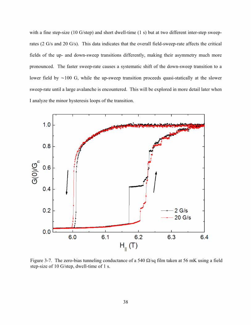
with a fine step-size (10 G/step) and short dwell-time (1 s) but at two different inter-step sweep-
rates (2 G/s and 20 G/s). This data indicates that the overall field-sweep-rate affects the critical
fields of the up- and down-sweep transitions differently, making their asymmetry much more
pronounced. The faster sweep-rate causes a systematic shift of the down-sweep transition to a
lower field by ~100 G, while the up-sweep transition proceeds quasi-statically at the slower
sweep-rate until a large avalanche is encountered. This will be explored in more detail later when
I analyze the minor hysteresis loops of the transition.
Figure 3-7. The zero-bias tunneling conductance of a 540 Ω/sq film taken at 56 mK using a field step-size of 10 G/step, dwell-time of 1 s.

39
The asymmetry of avalanche behavior is unusual. For instance, in the Barkhausen effect
non-thermal magnetic domain wall jumps produce avalanche-like features in the magnetization
loop of ferromagnetic alloys [17, 18]. However, Barkhausen avalanches are distributed symmetri-
cally across both branches of the hysteresis loop. Similarly, thermally induced martensitic
transitions exhibit avalanches when the sample is either cooled or heated through the critical region
[19]. The data in Figure 3-5 suggest that, when under the influence of a pure Zeeman field, the
system cannot find a continuous path out of the superconducting phase, but can make a continuous
transition from the normal state to the superconducting phase. Interestingly, the avalanches on the
superheating branch can be completely suppressed by tilting the film out of parallel orientation by
as little as 1.5° (see Figure 3-8), although the hysteresis remains mostly intact at such a small
misalignment. A misalignment of 1.5° corresponds to a perpendicular magnetic field of ∼ 0.15
T, which is an order of magnitude smaller than .
Figure 3-8. Angular dependence of the normalized zero-bias tunneling conductance of a film with = 562 Ω/sq taken at T = 52 mK.

40
A full systematic study of the influence of disorder on the details of the avalanche behavior
has not been done, but I have made tunneling measurements on films with normal state resistances
that are near the threshold of the superconductor-insulator transition [14] (i.e., ∼ /42 ≈ 6.5
kΩ/sq). These highly disordered films have rather broad critical field transitions (see Figure 3-2)
and a finite tri-critical point, but they do not exhibit avalanches. This study was focused primarily
on moderately disordered films. Shown in Figure 3-9 are the zero-bias tunneling conductance
versus parallel field hysteresis loops for films of varying sheet resistance (36 Ω/sq < < 540
Figure 3-9. Normalized zero-bias tunneling conductance versus parallel field (θ 0°) for films of varying taken at 80 mK.
41
Ω/sq). Consistent with the resistive transitions of Figure 3-2, a higher tendency for avalanches is
found in the 200 Ω/sq and 540 Ω/sq films. Interestingly, the parallel field (θ 0°) transitions of
the 36 Ω/sq and 70 Ω/sq films closely resemble those of the 562 Ω/sq film measured in tilted fields
(θ > 1.5°). Notice that in both scenarios the films exhibit: a small hysteresis-loop width, a zero-
bias tunneling conductance in the SC state that is relatively high, and a lack of avalanches during
their up-sweep transition. These features likely result from orbital-depairing effects, which can be
induced either by increasing the film thickness [20] (decreases ) or by increasing the transverse
field component [21] (increasing field-misalignment). If this is the case, then it furthers supports
the idea that these avalanches are intrinsic features of a purely Zeeman-limited SC condensate.
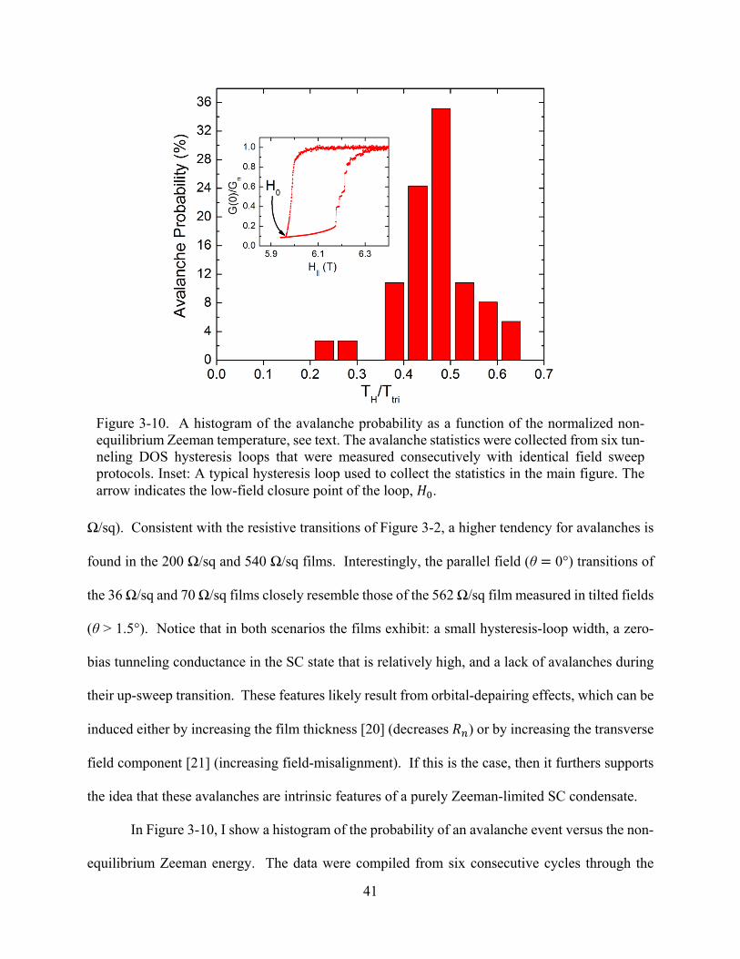
In Figure 3-10, I show a histogram of the probability of an avalanche event versus the non-
equilibrium Zeeman energy. The data were compiled from six consecutive cycles through the
Figure 3-10. A histogram of the avalanche probability as a function of the normalized non-equilibrium Zeeman temperature, see text. The avalanche statistics were collected from six tun-neling DOS hysteresis loops that were measured consecutively with identical field sweep protocols. Inset: A typical hysteresis loop used to collect the statistics in the main figure. The arrow indicates the low-field closure point of the loop, .

42
hysteresis loop. I define an effective non-equilibrium Zeeman temperature as 2 Δ / ,
where Δ is the extent to which the field has been ramped past the low-field closure
point of hysteresis loop , see inset of Figure 3-10. I believe that, as the field is ramped up into
the hysteretic region, the condensate is pushed further and further out of equilibrium by the
increasing Zeeman splitting. The parameter reflects this “stress”, which ultimately leads to an
avalanche. In producing the histogram, I normalized by the tricritical point temperature
730 mK. Note that the avalanche probability distribution of Figure 3-10 peaks near / ∼
0.45, which corresponds to 330 mK. Interestingly, this value of is consistent with
our observation that the avalanches disappear at temperatures above ∼300 mK, as can be seen
Figure 3-11.
Figure 3-11. Hysteresis in the normalized zero-bias tunneling conductance of the film in Figure 3-5 at various tri. Inset: The upper and lower parallel critical fields as a function of tem-perature determined from the midpoint of the critical field transitions as obtained from the zero-bias tunneling conductance.

43
Although it is generally accepted that even modest levels of disorder destroys the FFLO
phase [22], recent Hubbard calculations suggest that some vestiges of the FFLO state remain at
finite impurity densities [4]. There is no long-range FFLO order, but local modulations of the
pairing amplitude persist. In the critical field region, the order parameter develops positive and
negative regions that are separated by domain walls containing Andreev bound states. The domain
walls conform to the local disorder landscape so as to minimize the free energy of the system. The
tunneling data show that the system can readily optimize this domain wall configuration when
transitioning from the normal state to the superconducting state, but once the configuration is
formed, the domain walls remain pinned over a finite range of Zeeman fields. Consequently, as
one approaches the super-heating critical field branch, avalanches occur as a result of a
conflagration of domain wall de-pinning events.
The asymmetry of the non-equilibrium behavior is also evident in the minor hysteresis
loops shown in Figure 3-12. The upper panel shows a series of minor loops that were initiated
from the super-cooling branch. Each loop was swept out in succession at 30 s intervals. The
precipitous drop in tunnel conductance that precedes each of the minor loops is due to temporal
relaxation on the super-cooling branch. Note that, once off the branch, the minor loops exhibit
very little relaxation and all three loops return to their starting point and, hence, exhibit return point
memory [23]. Return point memory is generally not observed in first-order transitions that exhibit
drift in their hysteresis loop, but the supercooling minor loops in Figure 3-12 clearly show that the
system returns to its original state upon the completion of the loop and then continues drifting
downward. In contrast, the minor loops initiated from the superheating branch, shown in the lower
panel of Figure 3-12, are interspersed with multiple avalanches. Consequently, these do not
display return point memory. There is one notable exception, however.

44
Figure 3-12. Minor hysteresis loops of the zero-bias tunneling conductance for the film of Figure 3-5. The arrows indicate the field sweep direction. Upper panel: Minor loops off of the super-cooling branch taken in sequence with a 30 s interval between each. The upper minor loop was obtained by first halting the initial down-sweep at 6.02 T for 30 s. The field was then ramped up to 6.2 T and back to 6.02 T. This process was repeated twice more which resulted in the lower two minor loops. Lower panel: Minor loops off of the superheating branch. With each subsequent loop, the field was swept closer to the upper critical field and then returned to the initial sub-critical field of 5.9 T. The minor loop traces are labeled by their respective maximum field.

45
Figure 3-13 shows a magnified view of the superheating minor loops that return to their starting
point before ever encountering an avalanche. In this case, the transition is nearly reversible, until
the first avalanche occurs of course.
3.4 Conclusion
In summary, I have demonstrated that the condensate of a moderately disordered low-spin
orbit scattering, BCS superconductor exhibits asymmetric avalanche behavior near the Zeeman
critical field. The avalanches represent irreversible collapses of macroscopic regions of
superconductivity, but are not associated with magnetic flux jumps. Future studies of other low
atomic mass superconductors, which would presumably have differing film morphologies and
Figure 3-13. Magnified view of the minor hysteresis loops taken following the protocol used in the lower panel of Figure 3-12. The loops are nearly reversible before an avalanche event occurs.

46
superconducting parameters, should prove invaluable in further elucidating the origins and
characteristics of the non-equilibrium behavior of the Zeeman-limited superconducting state. For
instance, quenched-condensed Be films exhibit a first-order Zeeman-limited critical field transition
yet possess a non-granular, homogenously disordered morphology, in contrast to the granular
morphology of the Al films used in this study. Experiments on epitaxial Al films might also
provide a suitable control system to compare the effects of morphology on the dynamics. Another
option would be to rerun the simulations performed by Loh et al but this time incorporate uniform
and granular disorder into their model while also searching for avalanche behavior within the
hysteretic field region of the transition. However, to confirm whether the d-LO state truly exists
in these films, low temperature scanning tunneling microscopy would be ideal. Unfortunately,
there are many technical difficulties involved in performing these measurements at such low
temperatures. Nevertheless, in principle, the d-LO domain structure could be verified directly this
way.
3.5 References
[1] R. Beaird, A. B. Vorontsov, and I. Vekhter, Phys. Rev. B 81, 224501 (2010).
[2] T. J. Liu, J. C. Prestigiacomo, and P. W. Adams, Phys. Rev. Lett. 111, 027207 (2013).
[3] Y. M. Xiong, S. Stadler, P. W. Adams, and G. Catelani, Phys. Rev. Lett. 106, 247001 (2011).
[4] Y. L. Loh, N. Trivedi, Y. M. Xiong, P. W. Adams, and G. Catelani, Phys. Rev. Lett. 107, 067003 (2011).
[5] P. Fulde, Adv. Phys. 22, 667 (1973).
[6] W. H. Wu and P. W. Adams, Phys. Rev. Lett. 73, 1412 (1994).
[7] G. Catelani, Y. M. Xiong, X. S. Wu, and P. W. Adams, Phys. Rev. B 80, 054512 (2009).
[8] V. Y. Butko, P. W. Adams, and I. L. Aleiner, Phys. Rev. Lett. 82, 4284 (1999).
[9] V. Y. Butko, P. W. Adams, and E. I. Meletis, Phys. Rev. Lett. 83, 3725 (1999).

47
[10] B. S. Chandrasekhar, App. Phys. Lett. 1, 7 (1962).
[11] A. M. Clogston, Phys. Rev. Lett. 9, 266 (1962).
[12] W. H. Wu and P. W. Adams, Physical Review Letters 74, 610 (1995).
[13] T. I. Baturina, A. Y. Mironov, V. M. Vinokur, M. R. Baklanov, and C. Strunk, Phys. Rev. Lett. 99, 257003 (2007).
[14] S. M. Hollen, G. E. Fernandes, J. M. Xu, and J. M. Valles, Phys. Rev. B 87, 054512 (2013).
[15] M. Tinkham, (McGraw-Hill, New York, 1996).
[16] B. L. Altshuler, A. G. Aronov, M. E. Gershenson, and Y. V. Sharvin, Sov. Sci. Rev., Sect. A 9, 223 (1987).
[17] Z. Diao, E. R. Nowak, G. Feng, and J. M. D. Coey, Phys. Rev. Lett. 104, 047202 (2010).
[18] S. Papanikolaou, F. Bohn, R. L. Sommer, G. Durin, S. Zapperi, and J. P. Sethna, Nat Phys 7, 316 (2011).
[19] E. Vives, J. Ortín, L. Mañosa, I. Ràfols, R. Pérez-Magrané, and A. Planes, Phys. Rev. Lett. 72, 1694 (1994).
[20] X. S. Wu, P. W. Adams, and G. Catelani, Phys. Rev. B 74, 144519 (2006).
[21] W. H. Wu, R. G. Goodrich, and P. W. Adams, Phys. Rev. B 51, 1378 (1995).
[22] H. A. Radovan, N. A. Fortune, T. P. Murphy, S. T. Hannahs, E. C. Palm, S. W. Tozer, and D. Hall, Nature 425, 51 (2003).
[23] J. P. Sethna, K. Dahmen, S. Kartha, J. A. Krumhansl, B. W. Roberts, and J. D. Shore, Phys. Rev. Lett. 70, 3347 (1993).

48
CHAPTER 4. CONCLUSIONS
In conclusion, I have explored two separate yet related topics: a) half-metallic
ferromagnetism, and b) Zeeman-limited superconductivity. Both relate to so-called spin-
imbalanced systems, whose constituent materials range from the most basic and familiar (e.g. Fe,
Co, Ni), to the most exotic and obscure (e.g. cold atomic gases). Where these systems overlap,
tends to be the cutting edge of condensed matter physics research, and this is where the future
work of this dissertation lies. Although ferromagnetism and superconductivity rarely mix, a
combination of technological advancements and intuition-lead discoveries has deepened our
fundamental understanding of the two, allowing us to find a synergy between them. Before I
address this idea, however, it is prudent to recap the findings and implications of Chapters 2 and 3
separately.
I have shown experimentally that the half-metallic properties of Co2MnSi1-xAlx can indeed
be continuously tuned through chemical doping, and by extension, other Heuslers in this subclass
should have this ability as well. The fact that the Fermi energy shift is so pronounced in a series
of bulk, polycrystalline samples implies that further study of their single-crystalline counter-parts
is absolutely warranted. Moreover, engineering the gap-related properties of these materials in
thin film form can be achieved in many ways yet to be explored. From there, it is not hard to
conceptualize numerous devices that could implement these materials and enhance their
functionality.
I have also found substantial evidence that the disordered-Larkin-Ovchinnikov (d-LO)
phase exists in Zeeman-limited Al films. Finding concrete proof that Fulde-Ferrell-Larkin-
Ovchinnikov (FFLO) superconductivity exists in nature is an ambitious task indeed. However,
the approach I have taken, to start with d-LO SC in Al films and then work up from there, is a step

49
in the right direction. By looking for d-LO correlations in simple systems with moderate disorder
and then refining those systems to the highest attainable order, one has a good chance of
discovering the original FFLO phase, predicted over 40 years ago.
In closing, I think it is appropriate to mention that the original goal of this dissertation work
was to develop the SC probe and then use it to study various Heusler alloys. With the groundwork
described in this dissertation, one has a very good chance of achieving this. In principle, it is only
a technical challenge to observe Fermi level tuning in Co2MnSi1-xAlx via SC tunneling
spectroscopy. The main challenges are: 1) to keep clean interfaces between the films of the
junction, 2) to electrically isolate the electrode from the counter-electrode using the insulating
barrier layer, and 3) to avoid damaging the delicate Al electrode during fabrication of the Heusler
alloy counter-electrode. While all of these challenges can be met via elaborate thin film deposition
techniques, such as molecular beam epitaxy, the clever design of an in situ mask changing system
in a pulsed laser deposition system can achieve the same results, and with less time and financial
resources required. Furthermore, by incorporating advancements in the design of magnetic-tunnel-
junction barrier layers, there is a good possibility one can avoid the spin-depolarization effects that
plague the interfaces of many Heusler alloy films, thus using the SC probe to its full potential.

50
APPENDIX A1. HEUSLER ALLOY-BASED GIANT MAGNETO-IMPEDANCE EFFECT FIELD SENSOR: A PROPOSAL TO THE NATIONAL RESEARCH COUNCIL
A1.1 Introduction
I propose to develop a multipurpose, thin-film magnetometer that utilizes the giant
magneto-impedance (GMI) effect recently observed in Heusler alloys. Magnetic field sensors
are a ubiquitous technology and a variety of types exist (see Table A1-1). For many years now,
the instrument of choice has been the flux-gate magnetometer; however, their relatively large
sizes and high power requirements have precluded their implementation into microelectronic
devices. It has been suggested recently that the GMI effect could be used to design superior
magnetic-field [1], current [2], and stress sensors [3] for microelectronic devices where smaller
size, lower power, and higher sensitivities are required. The values of the GMI ratios (defined as
η (%) = 100*ΔZ/Z) and the field sensitivities (defined as ξ (%/Oe) = 2*(100*ΔZ/Z)max/ΔH,
where ΔH is the FWHM of the GMI curve), even at room temperature, greatly surpass those of
giant magneto-resistive devices; variations larger than 800%, and sensitivities well over
100%/Oe have been reported [4]. The sensing elements of GMI devices are available in three
structure types: microwires, ribbons, and thin films. Although used in numerous devices, such as
microwire-based electronic compasses in modern smart phones [5], the implementation of GMI-
based field sensors has been hampered by the difficulties in connecting microwires or ribbons to
the ancillary electronics. GMI thin films would work much better with integrated circuits
provided that their complex stoichiometry is not compromised and their current sensitivity (ξ ~
5-50 %/Oe) matches or surpasses that of ribbons (ξ ~ 30-150 %/Oe) or microwires (ξ ~ 10-300
%/Oe).

51
The highest performance thin film GMI sensors have come from multilayered
sandwiches comprised of FM (ferromagnetic)/non-FM metal/FM films, where the non-FM
metal, having a lower resistivity than the typical soft-FM materials used in conventional sensor
elements, is used to conduct the ac current while the FM layers couple to the flux. However, the
best-case scenario would be to achieve large GMI ratios and sensitivities from a single film
system, since these are easily fabricated and integrated into microchip circuitry.
Table A1-1. Several types of magnetic field sensors and their typical performance specifications.
Sensor type
Head length
Detectable field (Oe)
Resolution (Oe)
Response speed
Power required
Hall 10-100 µm 1-106 10 1 MHz 100 mW
Flux gate 10-20 mm 10-6-102 10-6 5 KHz 1 W
GMR 10-100 µm 0.1-102 1 1 MHz 10 mW
GMI (wire) 1-2 mm 10-8-102 10-6 1-5 MHz 10 mW
SQUID 1-10 mm 10-9-10-6 10-10 1 KHz 1 W
The research and development project that I propose directly addresses the above
concerns through the novel use of a Heusler alloy material in a thin film GMI sensor. Many of
the properties that are acquired by conventional GMI materials via complex doping and post-
processing are intrinsic to the Heusler alloys. Not only does this greatly simplify the fabrication
of these sensors in thin film form, but it also opens the door to realizing hybrid devices that take
full advantage of the many functional properties this material class exhibits (i.e. high spin-
polarization, shape-memory effects, and magneto-caloric properties, to name a few).
A1.2 Background
A1.2.1 The giant magneto-impedance effect
The giant magneto-impedance effect is a classical phenomenon that, in principle, should
be found in materials that exhibit 4 characteristics: a) low resistivity, b) soft ferromagnetism, c)

52
large saturation magnetization, and d) low damping parameter. When an ac current (~ mA) is
applied to such a magnetic conductor, an external dc magnetic field (a few Oe) will cause a large
change in the overall complex impedance. There are 3 mechanisms leading to this effect that are
dominant at different frequency ranges and the relative contribution of each is specific to a given
material and its shape. At low frequencies (~100 Hz – a few KHz) the impedance change is due
to a reduction in the transverse permeability that affects the inductance. At intermediate
frequencies (~100 KHz – a few MHz), where the GMI effect usually peaks, both the resistance
and the reactance are affected by field-induced variations of the skin depth. Finally, at high
Figure A1-1. Preliminary data (unpublished) of the GMI effect in bulk polycrystalline
Co2MnSi.

53
frequencies (several MHz – a few GHz) the skin depth is affected by ferromagnetic resonances,
provided the material has a low damping parameter.
A1.2.2 Heusler alloys
A class of highly multi-functional materials known as the Heusler alloys (HAs) has been
recently identified as showing GMI effects. I discovered this effect incidentally when I tried to
measure low-frequency magnetoresistance in Co2MnSi, a quintessential half-metal, and could
only observe a field response at frequencies above ~100 Hz (see Figure A1-1) [6]. To verify that
this behavior was not an artifact caused by stray capacitances and parasitic inductances in my
instrumentation, I constructed a 4-terminal-pair test probe to measure the impedance.
Interestingly, I observed a GMI ratio of ~60% at low temperature in a ~3 x 0.5 x 0.25 mm bulk
sample cut from a polycrystalline ingot synthesized by RF-induction [7]. This effect is usually
seen exclusively near room temperature in amorphous Co-based and nanocrystalline Fe-based
microwires and ribbons. At room temperature, the overall GMI ratio dropped to ~7%, however
the ratio of the reactive component of Z (100*ΔX/X) grew to ~80%. This behavior is consistent
with the low frequency range GMI effect discussed earlier. Later measurements of X taken at
frequencies near 1 KHz (not shown) would reach almost 300%.
Considering the properties that are required for a material to exhibit GMI, an observation
of this effect in Co2MnSi is consistent with the theories of GMI, and for the theory of spin-
polarization in HAs [8], for the following reasons: a) the material displays soft ferromagnetic
behavior due to the highly ordered L21 cubic structure of the compound, b) the high saturation
magnetization (5 µB/F.U.) arises due to Slater-Pauling behavior, and c) the high order-disorder
(L21 to B2) transformation temperature (~1400 K) enables the material to be easily synthesized
with negligible structural defects, hence its low resistivity.
54
A1.3 Methodology
The development of the proposed device will be a multi-stage process involving the
identification/synthesis/characterization of several Heusler candidates in thin film form, the
optimization of the deposition conditions to achieve the targeted structure for a single layer and
multilayer system, processing of the films into application specific patterns and their integration
into a working sensor system, and finally, performance testing of the device to establish sensor
sensitivity and directionality.
A1.3.1 Heusler candidates
Based on the aforementioned properties the most likely GMI candidate is Co2MnSi,
however, Co2FeAl is another suitable choice and among the vast number of HAs that may also
be considered. In principle, the upper limit of the operating temperature of the device is
determined by the Tc and ρ(T) < 100 Ω/cm. For HAs with low residual resistivity ratios (RRR)
the operating temperature can be broad. If only a narrow operating temperature range is
required, a HA with a Tc in that range will provide the best sensitivity.
A1.3.2 Thin film deposition
Two deposition techniques available at NRL that result in stoichiometric transfer of target
material to the substrate are sputtering and pulsed-laser deposition. The central task of the
deposition stage is to optimize the film growth parameters in order to balance the ideal magnetic
properties, which are generally found in amorphous or polycrystalline films, with the ideal
transport properties, which are typically found in an epitaxial structure. Use of the various
structural characterization techniques available at NRL to determine long-range crystalline order
(XRD), grain size and microstructure (SEM and TEM) and surface roughness and magnetic
55
domain distribution (AFM and MFM), will allow for an accurate assessment of the film
processing conditions.
The best MI behavior is expected to arise in soft ferromagnets with a well-defined easy
axis that lies transverse to the direction of the current [9]. Thus, it will be imperative to optimize
the domain structure in order to boost the MI performance of the films. The domain structure
and other magnetization processes are influenced by magnetocrystalline anisotropy, strain in the
film, and magnetostriction effects. The strain depends on the choice of substrate, growth
temperature, film thickness, and the resulting microstructure. By depositing on an amorphous
substrate such as glass, this strain can be reduced. Fortunately, it is possible to grow
polycrystalline Co2MnSi films on glass that exhibit single crystalline-like low resistivity values,
yet still possess low RRRs [10]. This, combined with its extremely high Curie temperature (Tc ~
1000 K), should stabilize the MI response across a broad temperature range.
At a thickness of ~100–200 nm, sputter deposited Co2MnSi can develop a columnar
microstructure [10], which tends to favor an out-of-plane anisotropy. However, more transverse
ac-flux (induced by the longitudinal ac-current) is contained within the material in a thicker film,
which enhances the skin effect. In addition, the film thickness will also determine the bandwidth
of the peak GMI response due to the frequency dependence of the skin depth [11]. Therefore, a
careful study of the thickness dependence of the GMI effect will be required.
Annealing procedures can significantly improve the physical properties of the films. For
example, by annealing the films in the presence of a transverse magnetic field it is possible to
relieve strain while simultaneously inducing an in-plane magnetic anisotropy [9, 11]. In
addition, by depositing films onto room temperature substrates, so that they are initially
amorphous, and then systematically annealing them at higher temperatures, it is possible to

56
balance surface roughness with the optimum crystallite size [10, 12]. Surface roughness is
detrimental to the skin effect and can degrade the interfaces of multilayered film structures as
well. One should note, however, that these procedures are only safe up to ~550° C for films
annealed on glass substrates. If higher temperatures are required, quartz or polycrystalline
sapphire substrates will suffice.
A1.3.3 Device fabrication
Three types of multilayers will be considered:
1) HA / non-FM transition metal / HA − (Co2MnSi / Au, Ag, or Cu / Co2MnSi)
2) HA / non-FM HA / HA − (Co2MnSi / Ni2NiSi / Co2MnSi)
3) [HA / SiOx]n / [non-FM metal] / [SiOx / HA]n − (SiOx -insulating barriers)
A non-FM metal spacer layer conducts the majority of the current through the film
sandwich, reducing eddy current formation in the ac electrical signal. The conventional, soft-FM
metals used in GMI sensors have a higher resistivity than non-FM metals, so this spacer type is
traditionally chosen to reduce current dissipation. However, the transport properties of Co2MnSi
films are ideal, so properly fabricated single films may display satisfactory magneto-impedance
characteristics. Nevertheless, using a conducting spacer metal of (Ag or Cu) induces (weak or
strong) effective magnetic anisotropy via interlayer coupling that is highly thickness dependent
and can be exploited to tune the frequency and field response [13]. As seen in Figure A1-2, SiOx
HA Non-FM metal
HA
SiOx
HA
Figure A1-2. An illustration of one possible configuration for the film sandwich comprising the sensor element. Note: Film layers are not to scale
Glass substrate

57
may be used both as a buffer layer between HA films (to interrupt columnar growth and increase
the overall thickness), and to create an insulating barrier between the FM and non-FM films (in
order to reduce flux leakage into the spacer metal).
The total film thickness of the sensor element will need to be approximately 1 µm, which
pushes the limits of conventional photolithography; however, patterning of the sensor structures
can be accomplished via the lift-off technique. Annealing treatments can be performed after
removal of the photoresist, but the substrate temperature during deposition should not exceed
160° C. Typical areal dimensions for a device are 10-30 µm x 2-5 mm, although many different
sized sensors can be patterned simultaneously to find the optimal aspect ratio.
A1.3.4 Sensor system configuration
A diagram of the basic experimental setup is given in Figure A1-3. The measurement
can be performed with a high output-current function generator and a dual-phase lock-in
amplifier. There are also RF-impedance analyzers better suited for these measurements that can
eliminate stray capacitances and parasitic inductances in the test apparatus. However, at
sufficiently high frequencies (typically GHz range) it is convenient to measure the reflection
coefficient of the signal with a network analyzer instead of measuring the voltage drop across the
film. These instruments are also used to conduct the performance testing described in the next
section and are available in the Materials Science Division at NRL.
The experimental setup described above is not the design limit of the device, however.
For example, by integrating the thin film sensing element into a circuit composed of a Colpitts
oscillation AM modulator-demodulator and a strong negative-feedback loop, a micro magnetic-
field sensor can be produced [1]. Some modification of this circuit would be necessary,
however, since its design is based on the use of GMI wire structure type.

58
A1.3.5 Performance testing
In order to quantify the sensitivity and directionality of the field sensor, I will utilize the
mechanical rotator and low-field options of the Quantum Design Physical Properties
Measurement System (PPMS) that is available at NRL. I have extensive experience operating a
similar PPMS instrument and designing RF-impedance test fixtures that are suitable for use in
cryogenic sample spaces. This is an important tool for testing the angular and temperature
dependence of field sensitivity. I will also be able to use this equipment to calibrate the devices.
Using a tabletop setup that includes a Helmholtz coil, I can also test the performance under non-
ideal operating conditions such as stray magnetic fields, vibrations, high temperatures, and
mechanical and chemical damage.
A1.4 Results
GMI sensors, such as the device envisioned in this proposal, can play an important role in
industrial and military applications. For instance, by combing multiple field sensors into a 3-axis
V+
V-
I+
I-
R
VRMS
AC LIA
H
+
-
Figure A1-3. Diagram of the most basic sensor design. The AC is provided by a function generator with an output current between 1- 100 mA and the magnitude is determined by measuring the voltage drop (VRMS) across a low inductance resistor (R) placed in series with the film. The resistive and reactive components of the impedance are measured with a dual-phase lock-in amplifier (LIA).

59
configuration, a highly accurate navigation device (an electric compass) can be fabricated for use
in guidance systems on many different platforms. Another example is the precise measurement
and control of gear-tooth positions and speeds in aircraft engines; a ferrous gear-tooth that moves
across such a sensor can be detected quickly due to its fast response time and small size. This
principle can be extended to a number of target detection applications by mounting a small
magnet to the object (target). Specific naval applications include low power, low cost
magnetometer arrays that can be placed in strategic locations on the sea floor in order to detect
submarines.
A1.5 Conclusion
I believe that the outcome of my proposed research will be of great benefit to the US
Navy and to other branches of the military, as well as the private sector. The demonstration of
GMI devices that feature materials as versatile and robust as the Heusler alloys has the potential
to pave the way for an entirely new class of hybrid devices. Utilizing these materials also makes
the fabrication of thin film GMI sensors less difficult and their quality more reproducible,
therefore making them more practical for large-scale production. My background in thin film
synthesis, materials characterization, and instrumentation as well as my experience with Heusler
alloys makes me well suited to conduct this research. Moreover, the available facilities at my
disposal at NRL will enable all development, characterization and testing aspects of this work. I
thank the National Research Council for their consideration of this proposal.
A1.6 References
[1] M. Kaneo, U. Tsuyoshi, and L. V. Panina, Sensor. Actuat. A-Phys. 59, 1 (1997).
[2] R. Valenzuela, J. J. Freijo, A. Salcedo, M. Vázquez, and A. Hernando, J Appl. Phys. 81, 4301 (1997).
[3] M. Tejedor, B. Hernando, M. L. Sánchez, V. M. Prida, and M. Vázquez, Sensor. Actuat A-Phys. 81, 98 (2000).

60
[4] X. P. Li, H. L. Seet, J. Fan, and J. B. Yi, J Magn. Magn. Mater. 304, 111 (2006).
[5] http://www.aichi-mi.com/.
[6] J. C. Prestigiacomo, D. P. Young, P. W. Adams, and S. Stadler, J Appl. Phys. 115, 043712 (2014).
[7] Unpublished measurements performed by author on 8/4/2012.
[8] I. Galanakis, P. H. Dederichs, and N. Papanikolaou, Phys. Rev. B 66, 174429 (2002).
[9] C. Tannous and J. Gieraltowski, J Mater. Sci.-Mater. El. 15, 125 (2004).
[10] M. P. Raphael, B. Ravel, M. A. Willard, S. F. Cheng, B. N. Das, R. M. Stroud, K. M. Bussmann, J. H. Claassen, and V. G. Harris, Appl. Phys. Lett. 79, 4396 (2001).
[11] M.-H. Phan and H.-X. Peng, Prog. in Mater. Sci. 53, 323 (2008).
[12] M. Obaida, K. Westerholt, and H. Zabel, Phys. Rev. B 84, 184416 (2011).
[13] A. M. H. de Andrade, M. A. Corrêa, A. D. C. Viegas, F. Bohn, and R. L. Sommer, J Appl. Phys. 115, 103908 (2014).
61
APPENDIX A2. CONSENT POLICY

62

63
VITA
Joseph Prestigiacomo received his Bachelor of Science degree in physics from Louisiana
State University in May 2009. While completing his bachelor’s degree, he worked part time as an
undergraduate research assistant under the supervision of Professor Philip Adams.
In August 2009, he entered graduate school at Louisiana State University in pursuit of a
Doctor of Philosophy degree in experimental condensed matter physics under the continued
guidance of Dr. Philip Adams. Along the way, he developed interests in disordered
superconductors (single- and multi-layered systems), multi-functional Heusler alloys (structural,
magnetic, electrical transport, magneto-caloric, and magneto-optical properties of these materials
in both bulk and thin-film form), and magnetic spin-glass systems (particularly, complex, rare-
earth based intermetallics). He is expected to receive his Doctor of Philosophy degree in December
2014.
Related Documents