1 1. INTRODUCTION Many analysts and policy makers have argued that building more highways is an Ineffective response to congestion: specifically, that it is infeasible to add enough highways Capacity in large urban areas to provide much relief. But this making of highways is just showing the path for accidents because of no speed limits in these highways. In order to overcome this problem we have designed equipment called as “SPEED CHECKER ON HIGHWAYS”. This kit investigates differentiated design standards as a source of capacity additions that are more affordable. Here we consider the average speed and high speed with which the vehicles are moving. We also consider the implications of differing accident rates. All these consideration were taken and the design of this equipment is done. This design helps to find the vehicles which are moving with high speed in spite of a speed limit board is present in that highway. The cops then can take necessary action on that culprit. The design mainly

Welcome message from author
This document is posted to help you gain knowledge. Please leave a comment to let me know what you think about it! Share it to your friends and learn new things together.
Transcript
1
1. INTRODUCTION
Many analysts and policy makers have argued that building more highways is an
Ineffective response to congestion: specifically, that it is infeasible to add enough highways
Capacity in large urban areas to provide much relief. But this making of highways is just
showing the path for accidents because of no speed limits in these highways. In order to
overcome this problem we have designed equipment called as “SPEED CHECKER ON
HIGHWAYS”. This kit investigates differentiated design standards as a source of capacity
additions that are more affordable. Here we consider the average speed and high speed with
which the vehicles are moving. We also consider the implications of differing accident rates.
All these consideration were taken and the design of this equipment is done. This design
helps to find the vehicles which are moving with high speed in spite of a speed limit board is
present in that highway. The cops then can take necessary action on that culprit. The design
mainly uses a timer, counter, logic gates and 7-segment display. Using these components we
design the speed checker on highways and observed that it is working more efficiently than
expected.
2
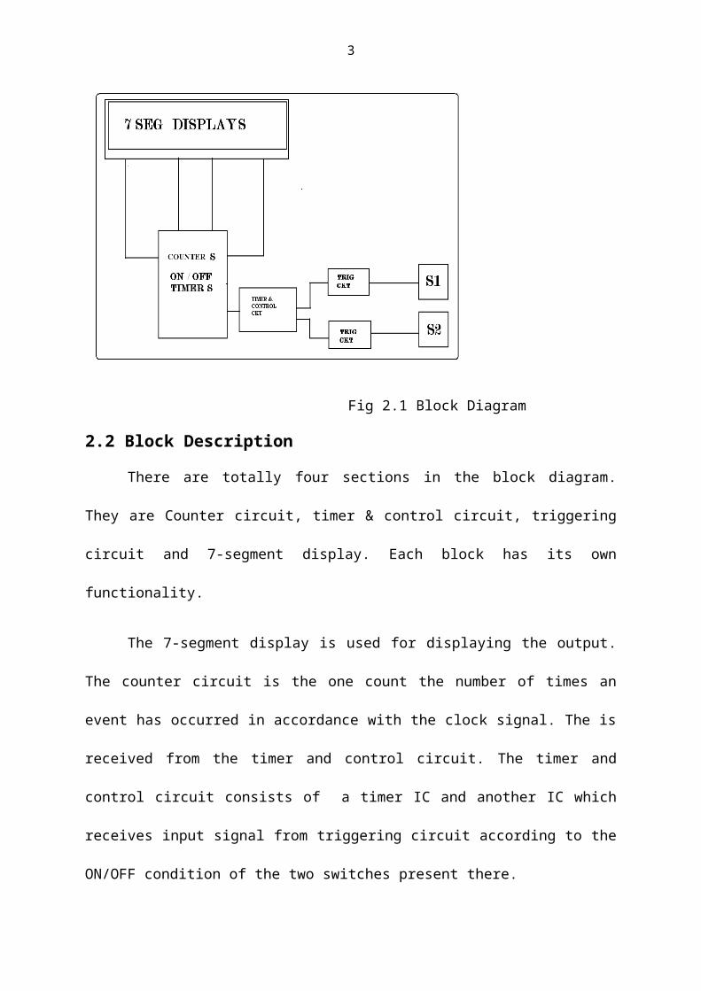
2. BLOCK DIAGRAM AND DESCRIPTION OF EACH BLOCK
2.1 Block Diagram
Fig 2.1 Block Diagram
2.2 Block Description
There are totally four sections in the block diagram. They are Counter circuit, timer &
control circuit, triggering circuit and 7-segment display. Each block has its own functionality.
The 7-segment display is used for displaying the output. The counter circuit is the one
count the number of times an event has occurred in accordance with the clock signal. The is
received from the timer and control circuit. The timer and control circuit consists of a timer
IC and another IC which receives input signal from triggering circuit according to the
ON/OFF condition of the two switches present there.
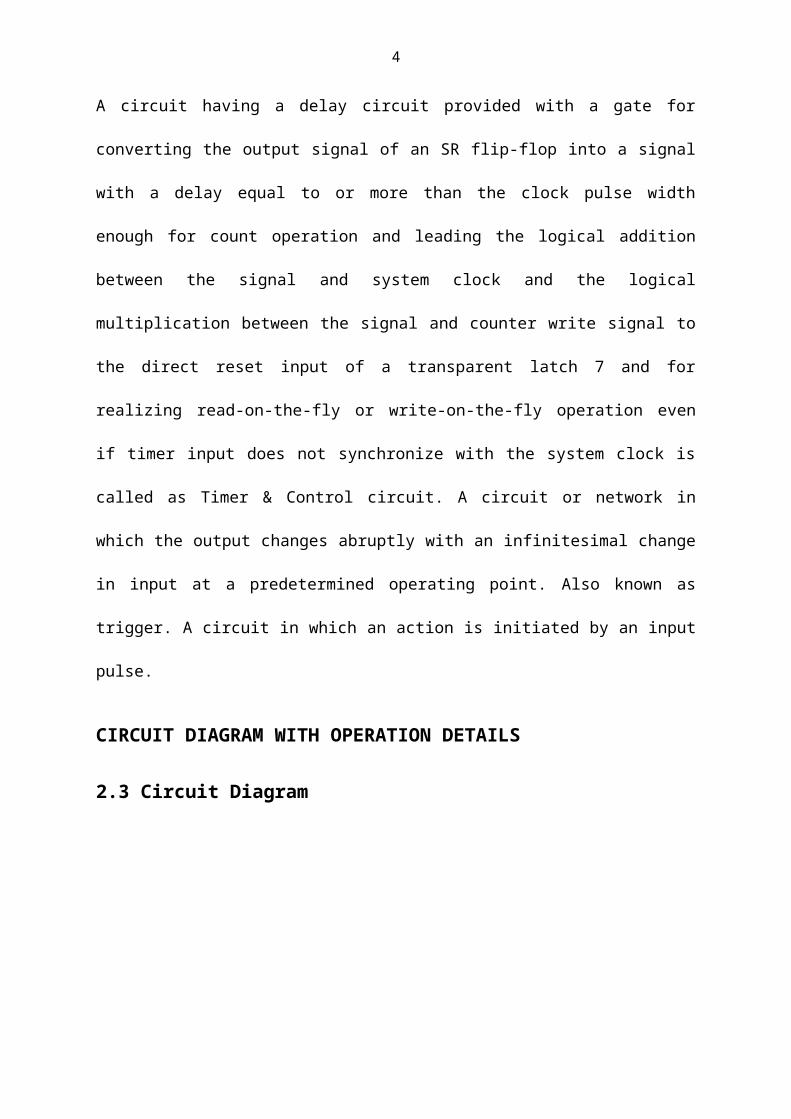
A circuit having a delay circuit provided with a gate for converting the output signal of an SR
flip-flop into a signal with a delay equal to or more than the clock pulse width enough for
3
count operation and leading the logical addition between the signal and system clock and the
logical multiplication between the signal and counter write signal to the direct reset input of a
transparent latch 7 and for realizing read-on-the-fly or write-on-the-fly operation even if
timer input does not synchronize with the system clock is called as Timer & Control circuit.
A circuit or network in which the output changes abruptly with an infinitesimal change in
input at a predetermined operating point. Also known as trigger. A circuit in which an action
is initiated by an input pulse.
CIRCUIT DIAGRAM WITH OPERATION DETAILS
2.3 Circuit Diagram
Fig 2.3 Circuit Diagram
4
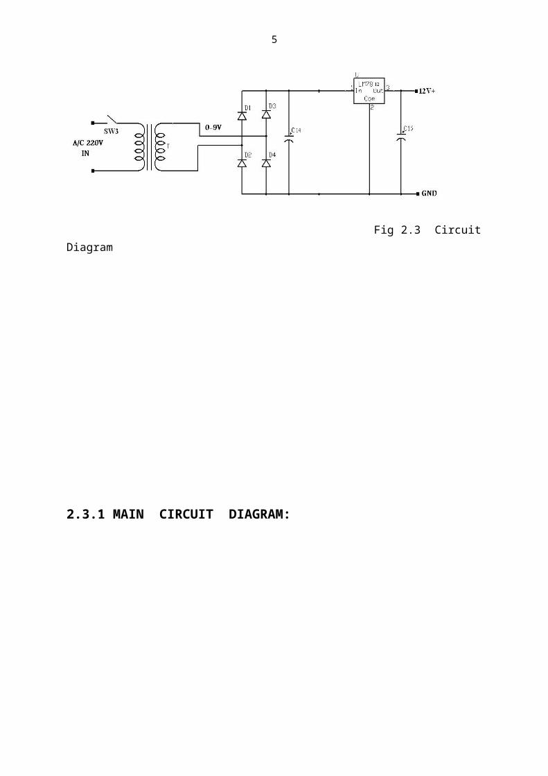
2.3.1 MAIN CIRCUIT DIAGRAM:
Fig 2.3.1 Main Circuit Diagram
2.4 circuit Operation:
The circuit mainly consists of a supply circuit, control circuit and a 7-segment display. The
control circuit consists of a counter ON/OFF circuit, timer & control circuit amd triggering
circuits connected to the switches.
When a supply is given to the secondary of the transformer, it steps down the 220v
AC supply to 18v AC. This 18v is fed to the bridge rectifier in order to convert AC to DC.
The bridge rectifier provides same polarity of output voltage for either polarity of input
voltage. It’s most common application is conversion of AC input to DC output. A capacitor
is connected across the output of bridge rectifier in order to reduce noise and fluctuations in
the output voltage. The 18v dc acts as input to the voltage regulator which reduces the
voltage to 12v,as only 12v is required to the circuit. This regulator uses a resistor to
maintain the voltage constant throughout the operation. This voltage is now fed to the
whole circuit.
5
The kit mainly consists of two laser transmitter-LDR sensor pairs which are installed on
the highway 100m apart such that the transmitter and LDR sensor of each pair on the
opposite sides of the road. This kind of arrangement is shown in the figure below.
Fig 2.4 Circuit Operation
When any vehicle crosses the first laser beam LDR1 goes high for the time set to cross
100mts with the selected speed (60KMPH) and LED1 glows during this period. When the
vehicle crosses the second laser light beam, the output of IC2 goes high and LED2 glows
for this period. Pezo buzzer sounds an alarm if the vehicle crosses the distance between the
laser setups at more than selected speed(lesser period than preset period).The counter starts
counting when the first laser beam is intercepted and stops when the second laser beam is
intercepted. The time taken by the vehicle to crop both the laser beams is displayed on the
7-segment display.
2.5 Supply Details:
Input supply to the transformer 220v AC
Input supply to the Bridge Rectifier 18v AC
Input supply to the Regulator 18v DC
Supply to the PCB 12v DC
6
3 COMPONENT DESCRIPTION
3.1 Transformer:
Transformer is static equipment which transforms power from one circuit to another by
stepping up or stepping down the primary voltage without any change in the frequency.
Fig 3.1 Transformer
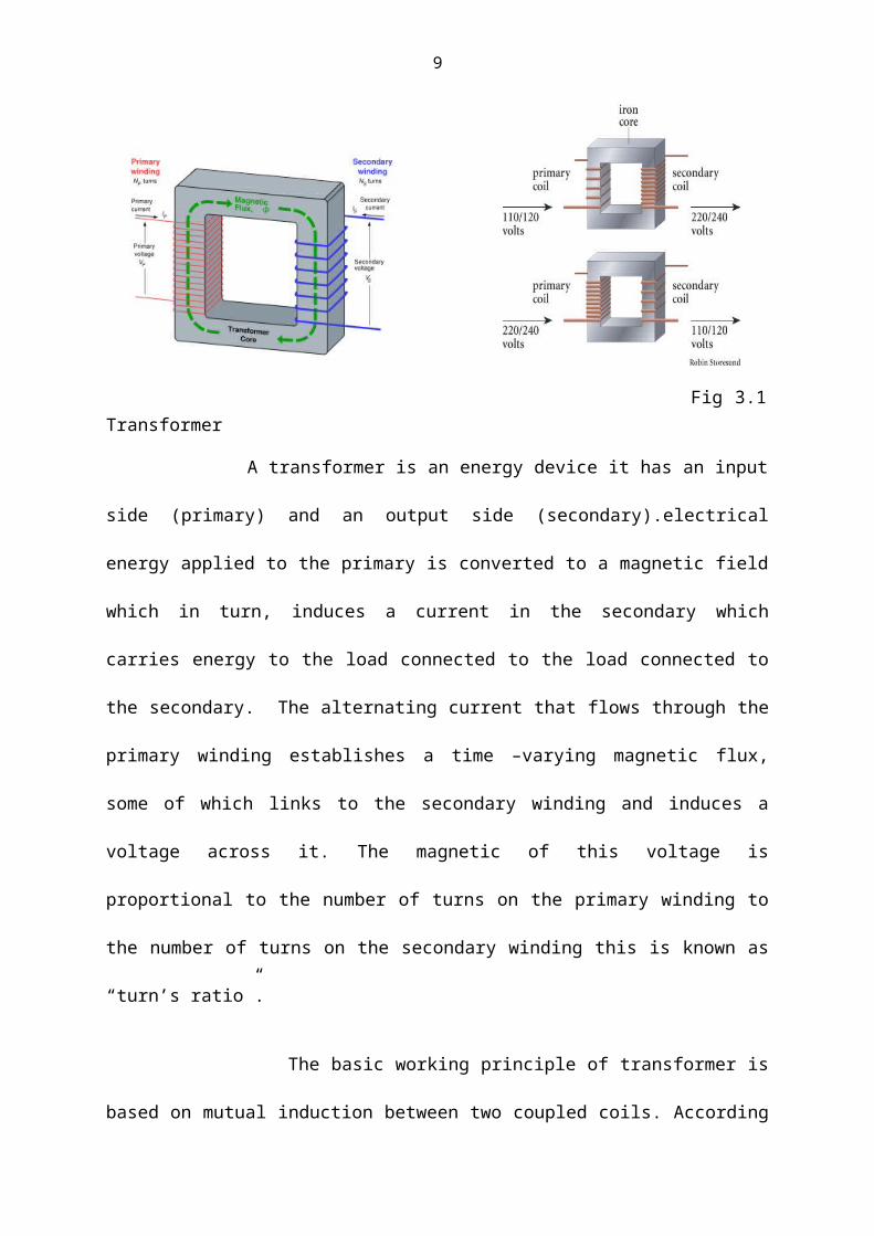
A transformer is an energy device it has an input side (primary) and an output side
(secondary).electrical energy applied to the primary is converted to a magnetic field which in
turn, induces a current in the secondary which carries energy to the load connected to the load
connected to the secondary. The alternating current that flows through the primary winding
establishes a time –varying magnetic flux, some of which links to the secondary winding and
induces a voltage across it. The magnetic of this voltage is proportional to the number of
turns on the primary winding to the number of turns on the secondary winding this is known
as “turn’s ratio”.
The basic working principle of transformer is based on mutual induction between
two coupled coils. According to this principle by changing flux creates on induced emf in
turn equal to the derivative of the flux so that the total induced emf across ‘N’ turns is

7
E= N d@/dt :- (@=fi)
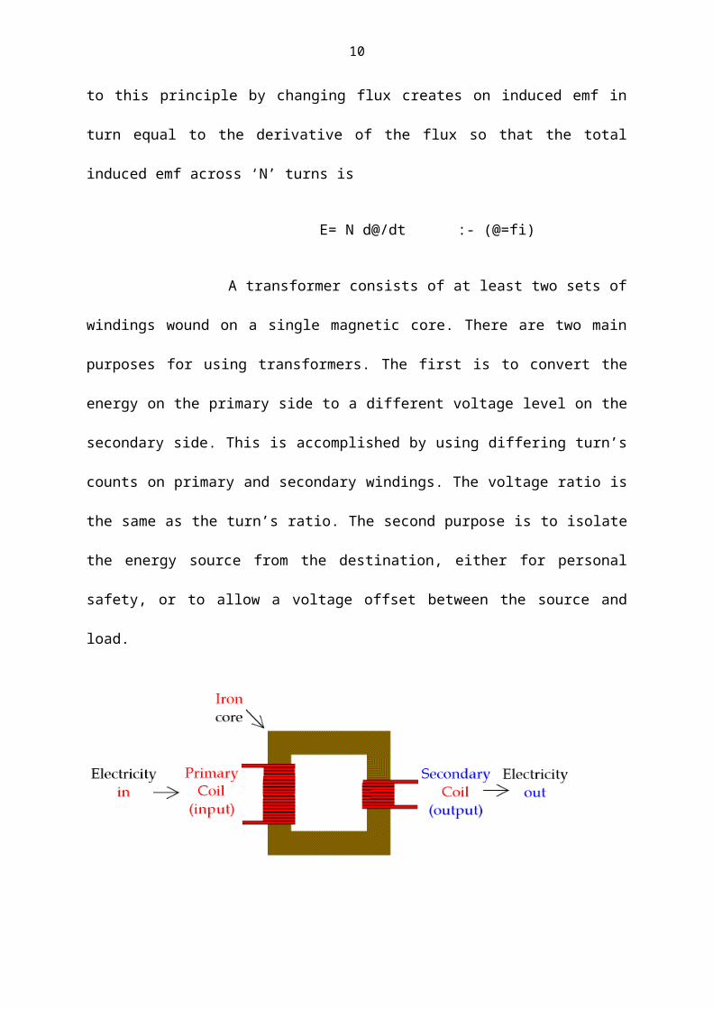
A transformer consists of at least two sets of windings wound on a single magnetic
core. There are two main purposes for using transformers. The first is to convert the energy
on the primary side to a different voltage level on the secondary side. This is accomplished
by using differing turn’s counts on primary and secondary windings. The voltage ratio is the
same as the turn’s ratio. The second purpose is to isolate the energy source from the
destination, either for personal safety, or to allow a voltage offset between the source and
load.
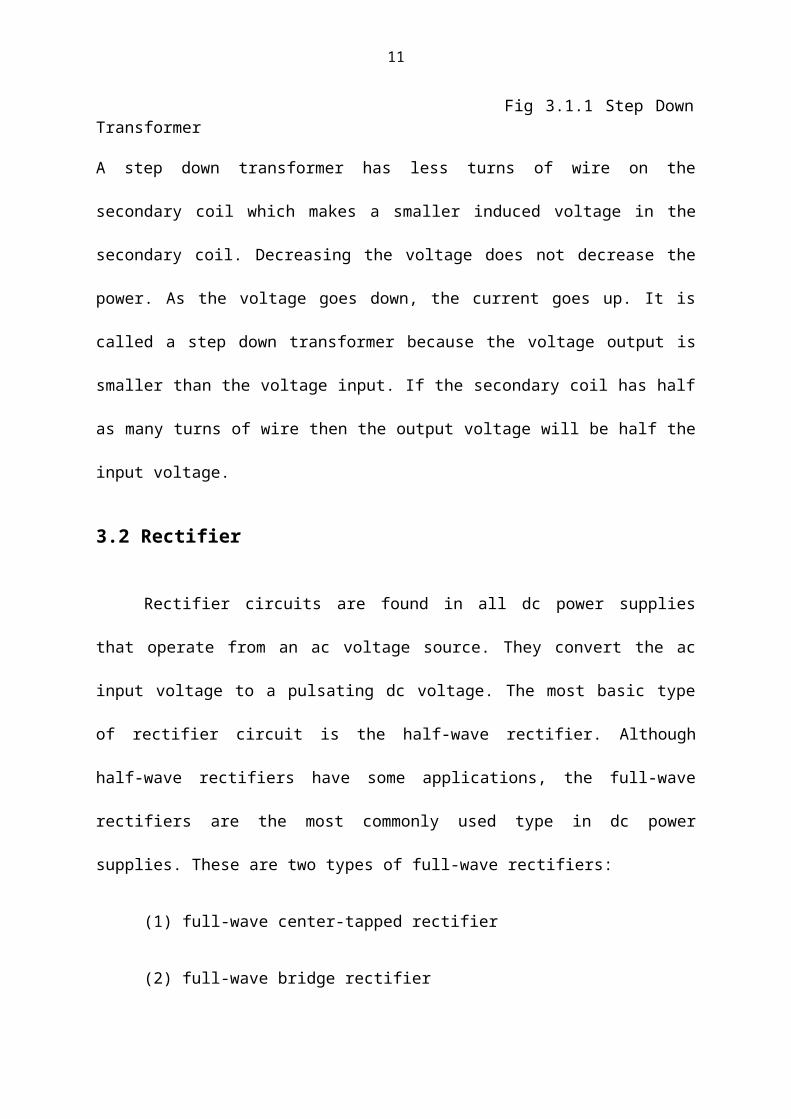
Fig 3.1.1 Step Down Transformer
A step down transformer has less turns of wire on the secondary coil which makes a smaller
induced voltage in the secondary coil. Decreasing the voltage does not decrease the power.
As the voltage goes down, the current goes up. It is called a step down transformer because
the voltage output is smaller than the voltage input. If the secondary coil has half as many
turns of wire then the output voltage will be half the input voltage.
3.2 Rectifier
Rectifier circuits are found in all dc power supplies that operate from an ac voltage
source. They convert the ac input voltage to a pulsating dc voltage. The most basic type of
8
rectifier circuit is the half-wave rectifier. Although half-wave rectifiers have some
applications, the full-wave rectifiers are the most commonly used type in dc power supplies.
These are two types of full-wave rectifiers:
(1) full-wave center-tapped rectifier
(2) full-wave bridge rectifier
Here in this particular design we are using a bridge rectifier which is discussed as
follows.
3.2.1 Full-wave Bridge Rectifier
The full –wave bridge rectifier uses four diodes, as shown in below figure. When the input
cycle is positive, diodes D1 and D2 are forward-biased and conduct current through RL.
During this time, diodes D3 and D4 are reverse-biased.
Fig 3.2 Full-wave Bridge Rectifier
During positive half-cycles of the input, D1 and D2 are forward-biased and conduct current, D3
and D4 are reverse-biased.
9
When the input cycle is negative as shown in below figure , diodes D3 and D4 are
forward-biased and conduct current in the same direction through RL as during the positive
half-cycle. During the negative half-cycle, D1 and D2 are reverse-biased. A full-wave rectifier
output voltage appears across RL as a result of this action.
During negative half-cycles of the input, D3 and D4 are forward-biased and conduct current
D1 and D2 are reverse-biased.
The above two figures explain the full-wave Bridge Rectifier.
The output graph of a full-wave rectifier is as shown
below
:
Fig 3.2.1 Diode Operation and waveform of current
10
3.2.2 IN4007 Diode
These diodes are used to convert AC into DC these are used as half wave rectifier or full
wave rectifier. Three points must he kept in mind while using any type of diode.
1. Maximum forward current capacity
2. Maximum reverse voltage capacity
3. Maximum forward voltage capacity
Fig 3.2.2 IN4007 Diode
The number and voltage capacity of some of the important diodes available in the market are
as follows:
Diodes of number IN4001, IN4002, IN4003, IN4004, IN4005, IN4006 and IN4007
have maximum reverse bias voltage capacity of 50V and maximum forward current
capacity of 1 Amp.
Diode of same capacities can be used in place of one another. Besides this diode of
more capacity can be used in place of diode of low capacity but diode of low capacity
cannot be used in place of diode of high capacity. For example, in place of IN4002;
IN4001 or IN4007 can be used but IN4001 or IN4002 cannot be used in place of
11
IN4007.The diode BY125made by company BEL is equivalent of diode from IN4001
to IN4003. BY 126 is equivalent to diodes IN4004 to 4006 and BY 127 is equivalent
to diode IN4007.
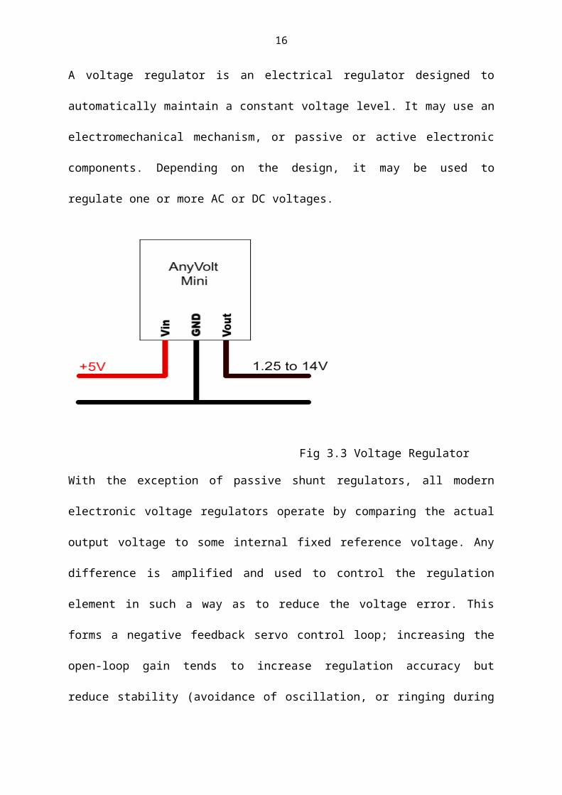
3.3 Voltage Regulator
A voltage regulator is an electrical regulator designed to automatically maintain a constant
voltage level. It may use an electromechanical mechanism, or passive or active electronic
components. Depending on the design, it may be used to regulate one or more AC or DC
voltages.
Fig 3.3 Voltage Regulator
With the exception of passive shunt regulators, all modern electronic voltage regulators
operate by comparing the actual output voltage to some internal fixed reference voltage. Any
difference is amplified and used to control the regulation element in such a way as to reduce
the voltage error. This forms a negative feedback servo control loop; increasing the open-loop
gain tends to increase regulation accuracy but reduce stability (avoidance of oscillation, or
ringing during step changes). There will also be a trade-off between stability and the speed of
the response to changes. If the output voltage is too low (perhaps due to input voltage

12
reducing or load current increasing), the regulation element is commanded, up to a point, to
produce a higher output voltage - by dropping less of the input voltage (for linear series
regulators and buck switching regulators), or to draw input current for longer periods (boost-
type switching regulators); if the output voltage is too high, the regulation element will
normally be commanded to produce a lower voltage. However, many regulators have over-
current protection, so entirely stop sourcing current (or limit the current in some way) if the
output current is too high, and some regulators may also shut down if the input voltage is
outside a given range (see also: crowbar circuits).
The voltage Regulator used in this design is LM 7812.
3.3.1 LM78xx Regulator
The LM78XX series of three terminal regulators is available with several fixed
output voltages making them useful in a wide range of applications. One of these is local on
card regulation, eliminating the distribution problems associated with single point regulation.
The voltages available allow these regulators to be used in logic systems, instrumentation,
Hi-Fi, and other solid state electronic equipment.
Although designed primarily as fixed voltage regulators these devices can be used with
external components to obtain adjustable voltages and currents. The LM78XX series is
available in an aluminum TO-3 package which will allow over 1.0A load current if adequate
heat sinking is provided. Current limiting is included to limit the peak output current to a safe
value. Safe area protection for the output transistor is provided to limit internal power
dissipation.
If internal power dissipation becomes too high for the heat sinking provided, the thermal
shutdown circuit takes over preventing the IC from overheating. Considerable effort was
expanded to make the LM78XX series of regulators easy to use and minimize the number of

13
external components. It is not necessary to bypass the output, although this does improve
transient response. Input bypassing is needed only if the regulator is located far from the filter
capacitor of the power supply.
For output voltage other than 5V, 12V and 15V the LM117 series provides an output voltage
range from 1.2V to 57V.
Features
- Output current in excess of 1A
- Internal thermal overload protection
- No external components required
- Output transistor safe area protection
- Internal short circuit current limit
- Available in the aluminum TO-3 package
Voltage Range
LM7805C 5V
LM7812C 12V
LM7815C 15V
3.4 IC 555 TIMER
The 555 Timer IC is an integrated circuit (chip) implementing a variety of timer and multi-
vibrator applications. The IC was designed and invented by Hans R. Camenzind. It was
14
designed in 1970 and introduced in 1971 by Signe tics (later acquired by Philips). The
original name was the SE555/NE555 and was called "The IC Time Machine".
The 555 gets its name from the three 5-kohm resistors used in typical early implementations.
It is still in wide use, thanks to its ease of use, low price and good stability. As of 2003, 1
billion units are manufactured every year. Depending on the manufacturer, it includes over 20
transistors, 2 diodes and 15 resistors on a silicon chip installed in an 8-pin mini dual-in-line
package (DIP-8). The 556 is a 14-pin DIP that combines two 555s on a single chip.
The 558 is a 16-pin DIP that combines four slightly modified 555s on a single chip (DIS &
THR are connected internally; TR is falling edge sensitive instead of level sensitive). Also
available are ultra-low power versions of the 555 such as the 7555 and TLC555. The 7555
requires slightly different wiring using fewer external components and less power.
The 555 has three operating modes:
• Monostable mode: in this mode, the 555 functions as a "one-shot". Applications
include timers, missing pulse detection, bounce free switches, touch switches, frequency
divider, capacitance measurement, pulse-width modulation (PWM) etc
• Astable - free running mode: the 555 can operate as an oscillator. Uses include LED
and lamp flashers, pulse generation, logic clocks, tone generation, security alarms, pulse
position modulation, etc.
• Bistable mode or Schmitt trigger: the 555 can operate as a flip-flop, if the DIS pin is
not connected and no capacitor is used. Uses include bounce free latched switches, etc.

15
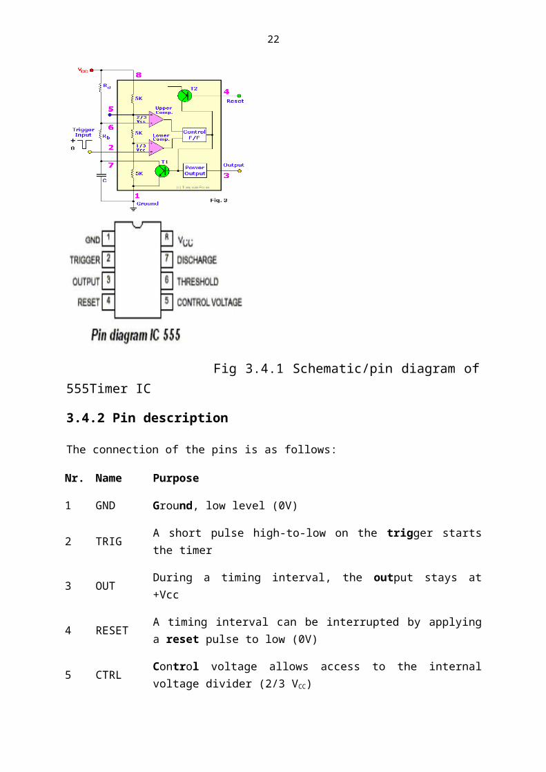
3.4.1 Schematic/pin diagram of 555Timer IC
Fig 3.4.1 Schematic/pin diagram of 555Timer IC
3.4.2 Pin description
The connection of the pins is as follows:
Nr. Name Purpose
1 GND Ground, low level (0V)
2 TRIG A short pulse high-to-low on the trigger starts the timer
3 OUT During a timing interval, the output stays at +Vcc
4 RESET A timing interval can be interrupted by applying a reset pulse to low (0V)
5 CTRL Control voltage allows access to the internal voltage divider (2/3 VCC)
6 THR The threshold at which the interval ends (it ends if U.thr → 2/3 VCC)
7 DISConnected to a capacitor whose discharge time will influence the timing interval
8 V+, VCC The positive supply voltage which must be between 3 and 15 V
3.4.3 APPLICATIONSThe timer, since introduction, has spurred the imagination of thousands. Thus, the ways in
which this device has been used are far too numerous to present each one. A review of the
basic operation and basic modes has previously been given.
16
Presented here are some ingenious applications.
a) Missing Pulse Detector
b) Pulse Width Modulation (PWM)
c) Pulse Position Modulation (PPM)
d) Tone Burst Generator
e) Sequential Timing
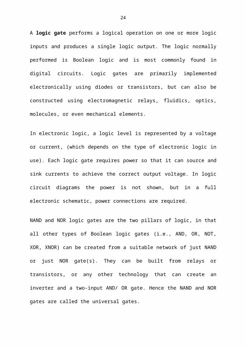
3.5 Logic Gate:
A logic gate performs a logical operation on one or more logic inputs and produces a single
logic output. The logic normally performed is Boolean logic and is most commonly found in
digital circuits. Logic gates are primarily implemented electronically using diodes or
transistors, but can also be constructed using electromagnetic relays, fluidics, optics,
molecules, or even mechanical elements.
In electronic logic, a logic level is represented by a voltage or current, (which depends on the
type of electronic logic in use). Each logic gate requires power so that it can source and sink
currents to achieve the correct output voltage. In logic circuit diagrams the power is not
shown, but in a full electronic schematic, power connections are required.
NAND and NOR logic gates are the two pillars of logic, in that all other types of Boolean
logic gates (i.e., AND, OR, NOT, XOR, XNOR) can be created from a suitable network of
just NAND or just NOR gate(s). They can be built from relays or transistors, or any other
17
technology that can create an inverter and a two-input AND/ OR gate. Hence the NAND and
NOR gates are called the universal gates.
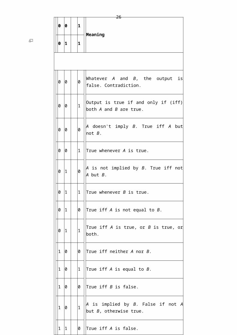
For an input of 2 variables, there are 16 possible Boolean algebraic functions. These 16
functions are enumerated below, together with their outputs for each combination of inputs
variables.
The four functions denoted by arrows are the logical implication functions. These functions
are generally less common, and are usually not implemented directly as logic gates, but rather
built out of gates like AND and OR.
18
0 0 1
Meaning
0 1 1
0 0 0 Whatever A and B, the output is false. Contradiction.
0 0 1 Output is true if and only if (iff) both A and B are true.
0 0 0 A doesn't imply B. True iff A but not B.
0 0 1 True whenever A is true.
0 1 0 A is not implied by B. True iff not A but B.
0 1 1 True whenever B is true.
0 1 0 True iff A is not equal to B.
0 1 1 True iff A is true, or B is true, or both.
1 0 0 True iff neither A nor B.
1 0 1 True iff A is equal to B.
1 0 0 True iff B is false.
1 0 1 A is implied by B. False if not A but B, otherwise true.
1 1 0 True iff A is false.
1 1 1 A implies B. False if A but not B, otherwise true.
1 1 0 A and B are not both true.
1 1 1 Whatever A and B, the output is true. Tautology.

19
The IC used in this design is CD4011 which is discussed as follows in the form of datasheet.
3.6 Counters:
In general, a counter is a device which stores (and sometimes displays) the number of times a
particular event or process has occurred, often in relationship to a clock signal. In practice,
there are two types of counters: In synchronous digital electronics, such as most computers, a
clock signal is a signal used to coordinate the actions of two or more circuits.
• Up counters which increase (increment) in value
• Down counters which decrease (decrement) in value
In electronics, counters can be implemented quite easily using register-type circuits such as
the flip-flop, and a wide variety of designs exist, e.g. Image File history File links T-flip-flop.
In digital circuits, the flip-flop, latch, or bi-stable multi-vibrator is an electronic circuit which
has two stable states and thereby is capable of serving as one bit of memory.
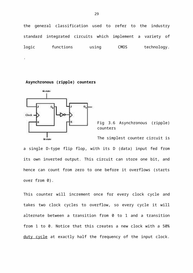
Asynchronous (ripple) counters
Synchronous counters
Johnson counters
Decade counters
Up-Down counters
Ring counters
Each is useful for different applications. Usually, counter circuits are digital in nature, and
count in binary, or sometimes binary coded decimal. Many types of counter circuit are
available as digital building blocks, for example a number of chips in the 4000 series
implement different counters. A digital system is one that uses discrete values (often
electrical voltages), especially those re-presentable as binary numbers, or non-numeric

20
symbols such as letters or icons, for input, processing, transmission, storage, or display,
rather than a continuous spectrum of values (i.e., as in an analog system). ... The term binary
code can mean several different things: There are a variety of different methods of coding
numbers or symbols into strings of bits, including fixed-length binary numbers, prefix codes
such as Huffman code, and other arithmetic coding. The 4000 series is the general
classification used to refer to the industry standard integrated circuits which implement a
variety of logic functions using CMOS technology. .
Asynchronous (ripple) counters
Fig 3.6 Asynchronous (ripple) counters
The simplest counter circuit is a single D-type flip flop, with its D (data) input fed from its
own inverted output. This circuit can store one bit, and hence can count from zero to one
before it overflows (starts over from 0).
This counter will increment once for every clock cycle and takes two clock cycles to
overflow, so every cycle it will alternate between a transition from 0 to 1 and a transition
from 1 to 0. Notice that this creates a new clock with a 50% duty cycle at exactly half the
frequency of the input clock. If this output is then used as the clock signal for a similarly
21
arranged D flip flop (remembering to invert the output to the input), you will get another 1 bit
counter that counts half as fast. Putting them together yields a two bit counter: Image File
history File links No higher resolution available. ... Image File history File links No higher
resolution available. ... In digital circuits, the flip-flop, latch, or bistable multivibrator is an
electronic circuit which has two stable states and thereby is capable of serving as one bit of
memory.
cycle Q1 Q0 (Q1:Q0)dec
0 0 0 0
1 0 1 1
2 1 0 2
3 1 1 3
4 0 0 0
You can continue to add additional flip flops, always inverting the output to its own
input, and using the output from the previous flip flop as the clock signal. The result is called
a ripple counter, which can count to 2n-1 where n is the number of bits (flip flop stages) in the
counter. Ripple counters suffer from unstable outputs as the overflows "ripple" from stage to
stage, but they do find frequent application as dividers for clock signals, where the
instantaneous count is unimportant, but the division ratio overall is. (To clarify this, a 1-bit
22
counter is exactly equivalent to a divide by two circuit - the output frequency is exactly half
that of the input when fed with a regular train of clock pulses). A ratio is a quantity that
denotes the proportional amount or magnitude of one quantity relative to another.
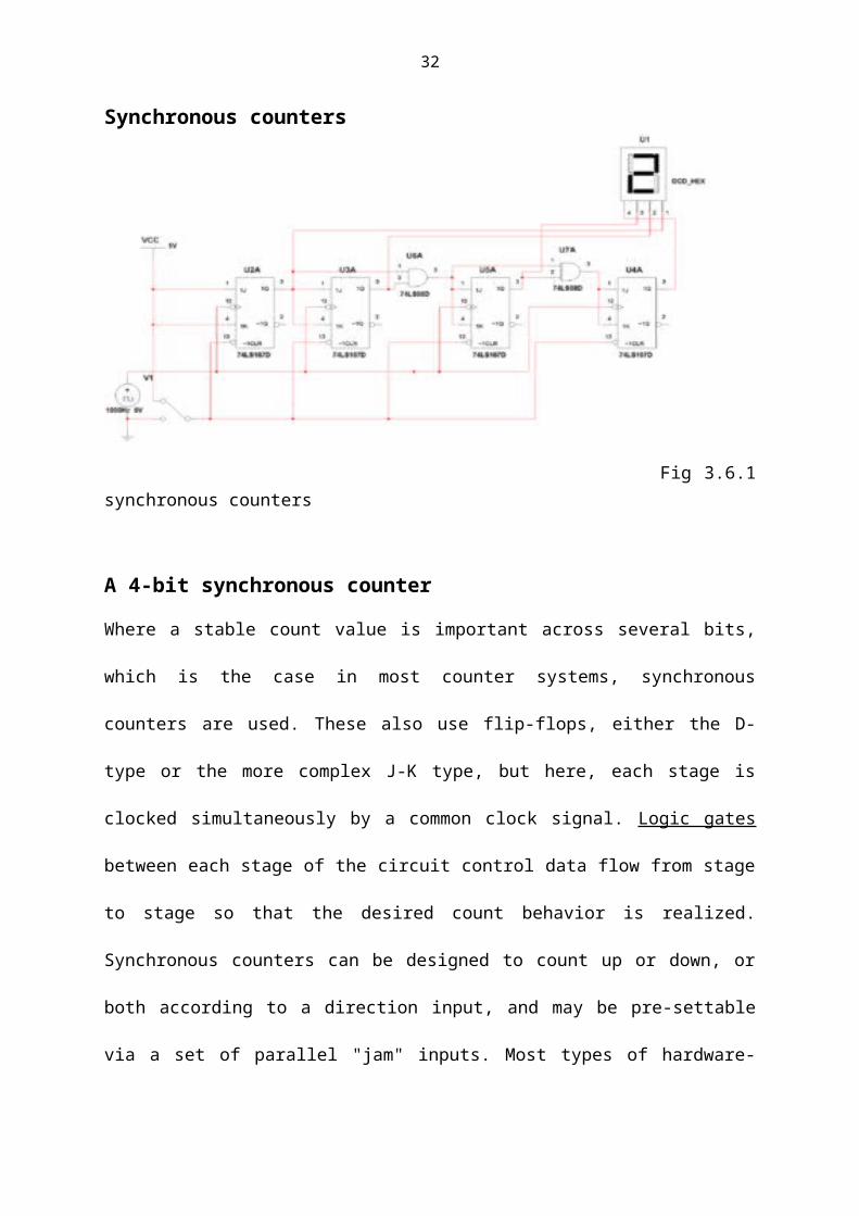
Synchronous counters
Fig 3.6.1 synchronous counters
A 4-bit synchronous counter
Where a stable count value is important across several bits, which is the case in most counter
systems, synchronous counters are used. These also use flip-flops, either the D-type or the
more complex J-K type, but here, each stage is clocked simultaneously by a common clock
signal. Logic gates between each stage of the circuit control data flow from stage to stage so
that the desired count behavior is realized. Synchronous counters can be designed to count up
or down, or both according to a direction input, and may be pre-settable via a set of parallel
"jam" inputs. Most types of hardware-based counter are of this type. Download high
resolution version (1712x943, 21 KB) Wikipedia does not have an article with this exact
name. A logic gate performs a logical operation on one or more logic inputs and produces a
single logic output.

23
Johnson counters
A Johnson counter is a special case of shift register, where the output from the last stage is
inverted and fed back as input to the first stage. A pattern of bits equal in length to the shift
register thus circulates indefinitely. These counters are sometimes called "walking ring"
counters, and find specialist applications, including those similar to the decade counter,
digital to analogue conversion, etc. In digital circuits a shift register is a group of registers set
up in a linear fashion which have their inputs and outputs connected together in such a way
that the data is shifted down the line when the circuit is activated.
Decade counters
Decade counters are a kind of counter that counts in tens rather than having a binary
representation. Each output will go high in turn, starting over after ten outputs have occurred.
This type of circuit finds applications in multiplexers and de-multiplexers, or wherever a
scanning type of behavior is useful. Similar counters with different numbers of outputs are
also common. Schematic of a 2-to-1 Multiplexer.
Up-Down Counters
It is a combination of up counter and down counter, counting in straight binary sequence.
There is an up-down selector. If this value is kept high, counter increments binary value and
if the value is low, then counter starts decrementing the count.
Ring CountersInstead of counting with binary numbers, a ring counter counts with words that have a single
high bit. These are ideal for timing a sequence of digital operations.
24
Counters in computer science
In computability theory, a counter is considered a type of memory. A counter stores a single
natural number (initially zero) and can be arbitrarily many digits long. A counter is usually
considered in conjunction with a finite state machine (FSM), which can perform the
following operations on the counter: In theoretical computer science a register machine is an
abstract machine used to study decision problems, similar to how a Turing machine is used.
In computer science, computability theory is the branch of the theory of computation that
studies which problems are computationally solvable using different models of computation.
In mathematics, a natural number can mean either an element of the set {1, 2, 3 ...} (i. ... 0
(zero) is both a number and a numerical digit used to represent that number in numerals.
Check whether the counter is zero
Increment the counter by one
Decrement the counter by one (if it's already zero, this leaves it unchanged).
The following machines are listed in order of power, with each one being strictly more
powerful than the one below it:
1. Deterministic or Non-deterministic FSM plus two counters
2. Non-deterministic FSM plus one stack
3. Non-deterministic FSM plus one counter
4. Deterministic FSM plus one counter
5. Deterministic or Non-deterministic FSM
For the first and last, it doesn't matter whether the FSM is deterministic or non-deterministic
(see determinism). They have equivalent power. The first two and the last one are levels of

25
the Chomsky hierarchy. Simple representation of a stack in computer science, a stack is a
temporary abstract data type and data structure based on the principle of Last In First Out
(LIFO). In the theory of computation, a deterministic finite state machine or deterministic
finite automaton (DFA) is a finite state machine where for each pair of state and input symbol
there is one and only one transition to a next state. The Chomsky hierarchy is a containment
hierarchy of classes of formal grammars that generate formal languages. The first machine,
an FSM plus two counters, is equivalent in power to a Turing machine. An artistic
representation of a Turing Machine. In theoretical computer science a register machine is an
abstract machine used to study decision problems, similar to how a Turing machine is
used.The Counter used in this design is a CMOS decade counter/divider which is discussed
as follows in the form of datasheet.
3.7 PCB DESIGN
Design and fabrication of printed circuit board or pcbs, form the core of
electronic equipment domestic and industrial. Some of the areas where PCB’s are intensively
used are computers, process control, telecommunications and instrumentation.
MANUFACTURING
The manufacturing process consists of two methods; print and etch, and print,
plate and etch. The single sided PCB’s are usually made using the print and etch method. The
double sided plate through hole (PTH) boards are made by the print plate and etch method.
The production of multi layer boards uses both the methods .The inner layers are printed and
etched while the outer layers are produced by print, plate and etch after pressing the inner
layers.
26
SOFTWARE
The software used in our project to obtain the schematic layout is MICROISM.
PANELISATION
Here the schematic transform in to the working positive/negative films .The circuit is
repeated conveniently to accommodate economically as many circuits are possible in a panel,
which can be operated in every sequence of subsequent steps in the PCB process. This is
called panelisation. For the PTH boards, the next operation is drilling.
RESISTORS
A resistor is a two-terminal passive electronic component that implements electrical
resistance as a circuit element. When a voltage V is applied across the terminals of a resistor,
a current I will flow through the resistor in direct proportion to that voltage. This constant of
proportionality is called conductance, G. The reciprocal of the conductance is known as
the resistance R, since, with a given voltage V, a larger value of R further "resists" the flow of
current I as given by Ohm's law:
Resistors are common elements of electrical networks and electronic circuits and are
ubiquitous in most electronic equipment. Practical resistors can be made of various
compounds and films, as well asresistance wire (wire made of a high-resistivity alloy, such as
nickel-chrome). Resistors are also implemented within integrated circuits, particularly analog
devices, and can also be integrated into hybridand printed circuits.
The electrical functionality of a resistor is specified by its resistance: common
commercial resistors are manufactured over a range of more than 9 orders of magnitude.

27
When specifying that resistance in an electronic design, the required precision of the
resistance may require attention to the manufacturing tolerance of the chosen resistor,
according to its specific application. The temperature coefficient of the resistance may also be
of concern in some precision applications. Practical resistors are also specified as having a
maximum power rating which must exceed the anticipated power dissipation of that resistor
in a particular circuit: this is mainly of concern in power electronics applications. Resistors
with higher power ratings are physically larger and may require heat sinking. In a high
voltage circuit, attention must sometimes be paid to the rated maximum working voltage of
the resistor.
Practical resistors include a series inductance and a small parallel capacitance;
these specifications can be important in high-frequency applications. In a low-noise
amplifier or pre-amp the noise characteristics of a resistor may be an issue. The unwanted
inductance, excess noise, and temperature coefficient are mainly dependent on the technology
used in manufacturing the resistor. They are not normally specified individually for a
particular family of resistors manufactured using a particular technology. A family of discrete
resistors is also characterized according to its form factor, that is, the size of the device and
position of its leads (or terminals) which is relevant in the practical manufacturing of circuits
using them.
First find the tolerance band, it will typically be gold ( 5%) and sometimes silver
(10%).
Now 'read' the next color, here it is red so write down a '2' next to the six. (you should
have '62' so far.)
Now read the third or 'multiplier exponent' band and write down that as the number of

28
zeros.
In this example it is two so we get '6200' or '6,200'. If the 'multiplier exponent' band is
Black (for zero) don't write any zeros down.
If the 'multiplier exponent' band is Gold move the decimal point one to the left. If the
'multiplier exponent' band is Silver move the decimal point two places to the left. If the
resistor has one more band past the tolerance band it is a quality band.
Read the number as the '% Failure rate per 1000 hour' This is rated assuming full
wattage being applied to the resistors. (To get better failure rates, resistors are typically
specified to have twice the needed wattage dissipation that the circuit produces). Some
resistors use this band for temco information. 1% resistors have three bands to read
digits to the left of the multiplier. They have a different temperature coefficient in order
to provide the 1% tolerance.
At 1% the temperature coefficient starts to become an important factor. at +/-200 ppm
a change in temperature of 25 Deg C causes a value change of up to 1%
29
Fig 3.7.1 Resistor colour coding
CAPACITOR
Fig3.7.2. A Typical Electrolytic Capacitor
A capacitor (formerly known as condenser) is a device for storing electric charge. The forms
of practical capacitors vary widely, but all contain at least two conductors separated by a non-

30
conductor. Capacitors used as parts of electrical systems, for example, consist of metal foils
separated by a layer of insulating film.
A capacitor is a passive electronic component consisting of a pair
of conductors separated by a dielectric (insulator). When there is a potential
difference (voltage) across the conductors, a staticelectric field develops across the dielectric,
causing positive charge to collect on one plate and negative charge on the other
plate. Energy is stored in the electrostatic field. An ideal capacitor is characterized by a single
constant value, capacitance, measured in farads. This is the ratio of the electric charge on
each conductor to the potential difference between them.
Capacitors are widely used in electronic circuits for blocking direct current while
allowing alternating current to pass, in filter networks, for smoothing the output of power
supplies, in the resonant circuits that tune radios to particular frequencies and for many other
purposes.
The capacitance is greatest when there is a narrow separation between large areas of
conductor; hence capacitor conductors are often called "plates," referring to an early means of
construction. In practice the dielectric between the plates passes a small amount of leakage
current and also has an electric field strength limit, resulting in a breakdown voltage, while
the conductors and lead sintroduce an undesired inductance and resistance.

31
4. IMPLEMENTATION AND TROUBLESHOOTING
4.1 Implementation
The kit can be implemented on a highway as shown in the figure below.
Fig 4.1 Implementation circuit
4.2 Trouble shooting
Clear of any dust on PCB with white paper towel soaked in thinner/acetone(nail
polish remover).
Check correct polarity of the power supply before connecting power to the circuit.
In the circuit use long wires for connecting the two LDR’s, so that we can take them
out and install on highway 100mts apart easily.
Install the two laser light transmitters exactly opposite to the LDR’s so that the laser
light falls on them exactly.
32
Reset the circuit by pressing the preset button , S2, so that the display shows ‘0000’.
Using S1, select the speed limit on the highway, say 60KMPH.
For 60Kmph setting with frequency set at 100Hz,if the display count is less than ‘600’
then it indicates that vehicle has crossed the speed limit and simultaneously the buzzer
sounds.
Reset the circuit for monitoring the speed of the vehicle.
5 RESULT:
Thus the design has tested the speed of a vehicle when the vehicle is passed through
those two pairs of transmitter-LDR pairs. Here it can check the speed of a single vehicle only.
6 CONCLUSION & FUTURE SCOPE
6.1 Conclusion:
Hence we conclude that by using the speed checker on Highways we can measure the
speed of a single vehicle at a time only.
6.2 Future scope:
This kit be still extended to speed checking of multiple vehicles by using a
microcontroller.
This can also be extended to count the number of vehicles.
The design for sending a message when an accident occurs can be done by this by
installing it in a accident prone zones with some necessary add-ups.

33
BIBLIOGRAPHY
www.alldatasheets.com
www.digikey.com
www.wikipedia.com
www.electronicslab4u.com
Electronic devices and circuits By Louis boylsted and Naschalsky.
Switching Theory and Logic Design By Jain,RP
Linear Integrated circuits By Roy choudhary
COMPONENT VALUE
Resistors 1,4 100k ohms
Resistors 2,5,6,810,11,14 10k ohms
Resistors 3,7,13,16,17,18,19 470 ohms
Resistor 9 470k ohms
Resistors 12,15 1 k ohms
Variable Resistors VR1,VR2 100 k ohms
Variable Resistors VR3 20k ohms
Capacitor 1 100 micro farads,25 v
Capacitors 2,4,6,8,11 0.01 micro farad, disk
Capacitors 3,13,15 0.1 micro farad, disk
Capacitor 5 10 micro farad,25v
Capacitor 7 0.47 micro farad,63v (electrolytic)
Capacitor 9 0.2 micro farad, disk
34
Capacitor 10 1 micro farad, 25v
LDR 1,2 10 mm(ldr)
Capacitor 12 47 micro farad,25v
Capacitor 14 1000 micro farad,35v
IC’S 1,2,3,4,5 NE 555
IC’S 6,7,8,9 CD 4026
IC 10 CD4011BE
IC 11 7812
LED 1 Green
LED 2,3 Red
Display 1,2,3,4 LT-543 seven segment display
Piezobuzzer
Switch 1 SPDT on –off switch
Switch 2 Push to on switch
Switch 3 On/off switch
Table 1.1 Components and their values
Related Documents