This document is subject to Anders Electronics plc’s standard terms and conditions of sale. Prior to concluding any agreement with Anders Electronics plc, the customer should satisfy itself of the accuracy and completeness of the information contained herein and should notify Anders of any intended use of the product. anders electronics plc | Kings Studios, 43-45 Kings Terrace, London, NW1 0JR | Tel: +44(0)20 7388 7171| Fax: +44(0)20 7383 2423 | www.andersDX.com | [email protected] Specification for Colour TFT Display module 12.3” Ultra-Wide Screen 21:9 aspect ratio colour TFT module Manufacturer Truly Semiconductors LTD Part n˚ TFT1920720-1 Ordering n˚ TFT1920720-1-E Customer Part n˚ n/a Revision n˚ 1.0 Issue Date 2016/11/28 Customer’s Approval Company name Printed name Job title Signature Approval Stage: This product is approved for the following production stage: - Sample / Prototype Pre-Production Mass Production Approval Date Supplied by Anders Electronics plc Manufactured by Truly Semiconductors LTD

Welcome message from author
This document is posted to help you gain knowledge. Please leave a comment to let me know what you think about it! Share it to your friends and learn new things together.
Transcript
This document is subject to Anders Electronics plc’s standard terms and conditions of sale. Prior to concluding any agreement with Anders Electronics plc, the customer should satisfy itself of the accuracy and completeness of the information contained herein and should notify Anders of any intended use of the product. anders electronics plc | Kings Studios, 43-45 Kings Terrace, London, NW1 0JR | Tel: +44(0)20 7388 7171| Fax: +44(0)20 7383 2423 | www.andersDX.com | [email protected]
Specification for Colour TFT Display module 12.3” Ultra-Wide Screen 21:9 aspect ratio colour TFT
module
Manufacturer Truly Semiconductors LTD
Part n˚ TFT1920720-1 Ordering n˚ TFT1920720-1-E
Customer Part n˚ n/a Revision n˚ 1.0
Issue Date 2016/11/28
Customer’s Approval
Company name
Printed name Job title
Signature
Approval Stage:
This product is approved for the following production stage: -
Sample / Prototype
Pre-Production
Mass Production Approval Date
Supplied by Anders Electronics plc
Manufactured by Truly Semiconductors LTD
TRULY SEMICONDUCTORS LTD. CONFIDENTIAL P.1
SPECIFICATION
This module uses RoHS compliant material
TRULY SEMICONDUCTORS LTD: CUSTOMER:
PRODUCT : LCD MODULE PRODUCT NO. : TFT1920720-1
SUPPLIER : TRULY SEMICONDUCTORS LTD.
REVERION : 1.0
Quality Assurance Department: Approved by: Technical Department:
Approved by:
If there is no special request from the customer, TRULY SEMICONDUCTORS LTD. will not reserve the tooling of the product under the following conditions: 1.There is no response from the customer in two years after TRULY SEMICONDUCTORS LTD. submit the samples. 2.There is no order in five years after the latest mass production. And correlated data (including quality records) will be reserved for one year more after tooling is discarded.
TRULY SEMICONDUCTORS LTD. CONFIDENTIAL P.2
REVISION RECORD
REV NO. REV DATE CONTENTS REMARKS
1.0 2016.11.28
WRITTEN BY CHECKED BY APPROVED BY
黄建生,张文峰 欧阳剑飞 万志强
TRULY SEMICONDUCTORS LTD. CONFIDENTIAL P.3
CONTENTS
SPECIFICATION ............................................................................................. 1
1) GENERAL INFORMATION ................................................................ 4
2) EXTERNAL DIMENSIONS ................................................................. 5
3) ABSOLUTE MAXIMUM RATINGS ................................................... 6
4) ELECTRICAL CHARACTERISTICS ................................................ 6
5) BACKLIGHT CHARACTERISTICS .................................................. 7
6) ELECTRO-OPTICAL CHARACTERISTICS ................................... 8
7) INTERFACE DESCRIPTION ............................................................. 11
8) TIMING CHARACTERISTICS ......................................................... 12
9) REFERENCE APPLICATION CIRCUIT ....................................... 16
10)RECOMMENDED INITIALIZATION .......................................... 16
11) RELIABILITY TEST ......................................................................... 17
12) INSPECTION CRITERIA ................................................................. 18
13) PRECAUTIONS FOR USING LCD MODULES ............................ 22
1 Handling Precautions ..................................................................... 22
2 Handling precaution (pictorial) ..................................................... 23
3 Storage Precautions ........................................................................ 24
4 Safety ................................................................................................ 24
5 Others ............................................................................................... 24
14) PACKING SPECIFICATION ............................................................ 24
TRULY SEMICONDUCTORS LTD. CONFIDENTIAL P.4
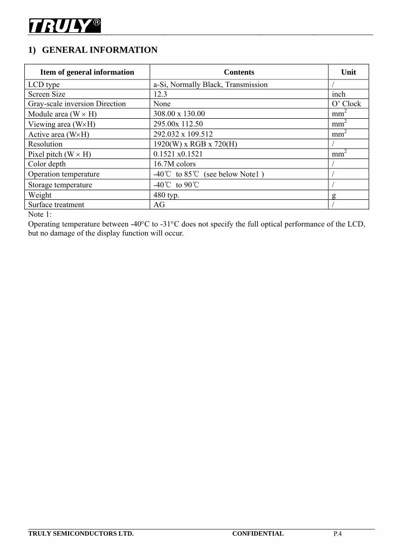
1) GENERAL INFORMATION
Item of general information Contents Unit
LCD type a-Si, Normally Black, Transmission / Screen Size 12.3 inch Gray-scale inversion Direction None O’ Clock Module area (W H) 308.00 x 130.00 mm2 Viewing area (WH) 295.00x 112.50 mm2 Active area (WH) 292.032 x 109.512 mm2 Resolution 1920(W) x RGB x 720(H) / Pixel pitch (W H) 0.1521 x0.1521 mm2 Color depth 16.7M colors / Operation temperature -40 to 85 (see below Note1 ) / Storage temperature -40 to 90 / Weight 480 typ. g Surface treatment AG / Note 1: Operating temperature between -40C to -31C does not specify the full optical performance of the LCD, but no damage of the display function will occur.
TRULY SEMICONDUCTORS LTD. CONFIDENTIAL P.5
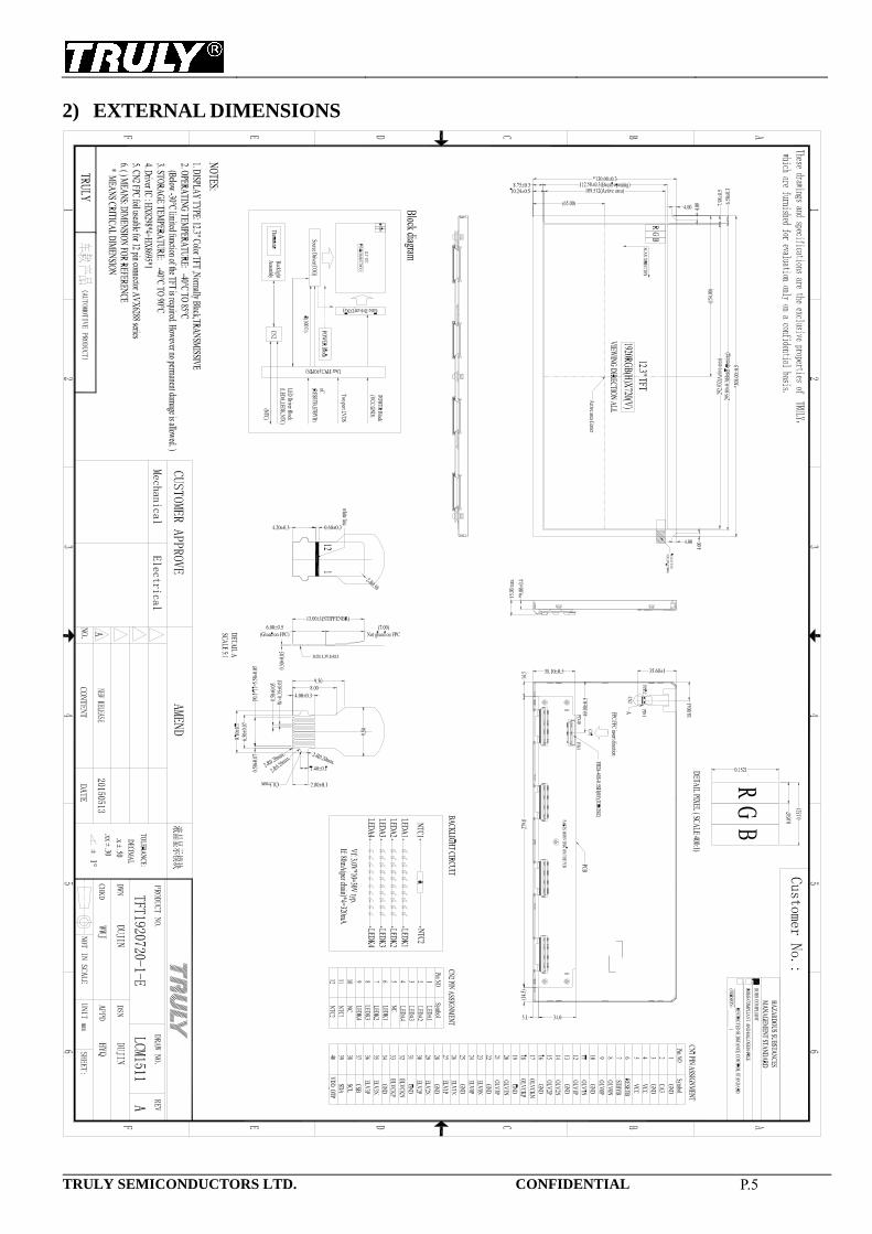
2) EXTERNAL DIMENSIONS
TRULY SEMICONDUCTORS LTD. CONFIDENTIAL P.6
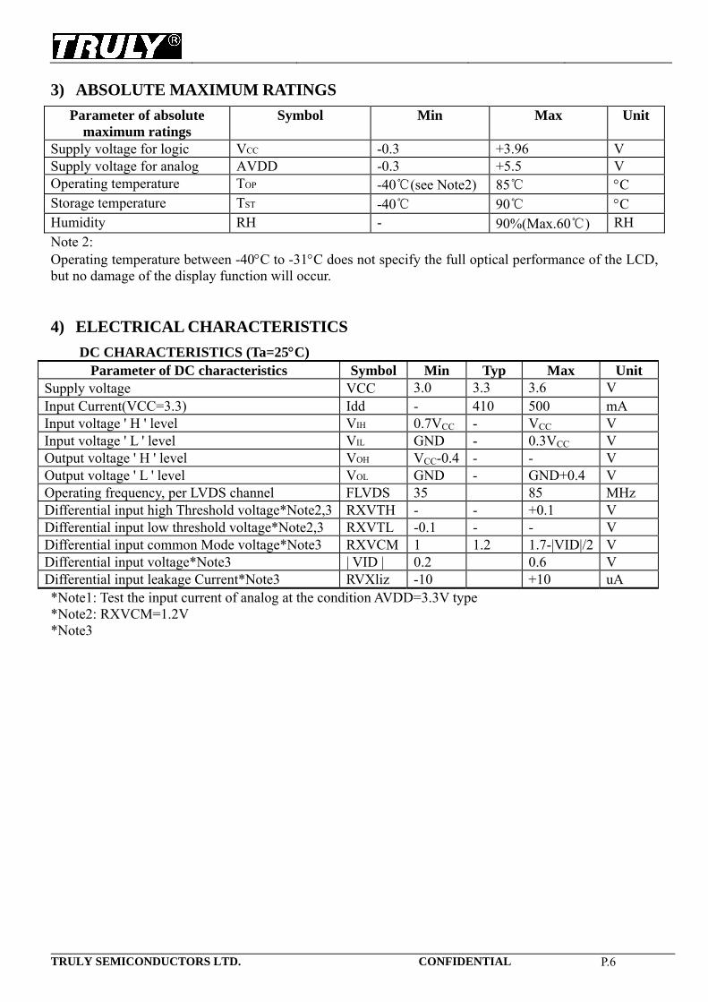
3) ABSOLUTE MAXIMUM RATINGS
Parameter of absolute maximum ratings
Symbol Min Max Unit
Supply voltage for logic VCC -0.3 +3.96 V Supply voltage for analog AVDD -0.3 +5.5 V Operating temperature TOP -40(see Note2) 85 C Storage temperature TST -40 90 C Humidity RH - 90%(Max.60) RH Note 2: Operating temperature between -40C to -31C does not specify the full optical performance of the LCD, but no damage of the display function will occur. 4) ELECTRICAL CHARACTERISTICS
DC CHARACTERISTICS (Ta=25C) Parameter of DC characteristics Symbol Min Typ Max Unit
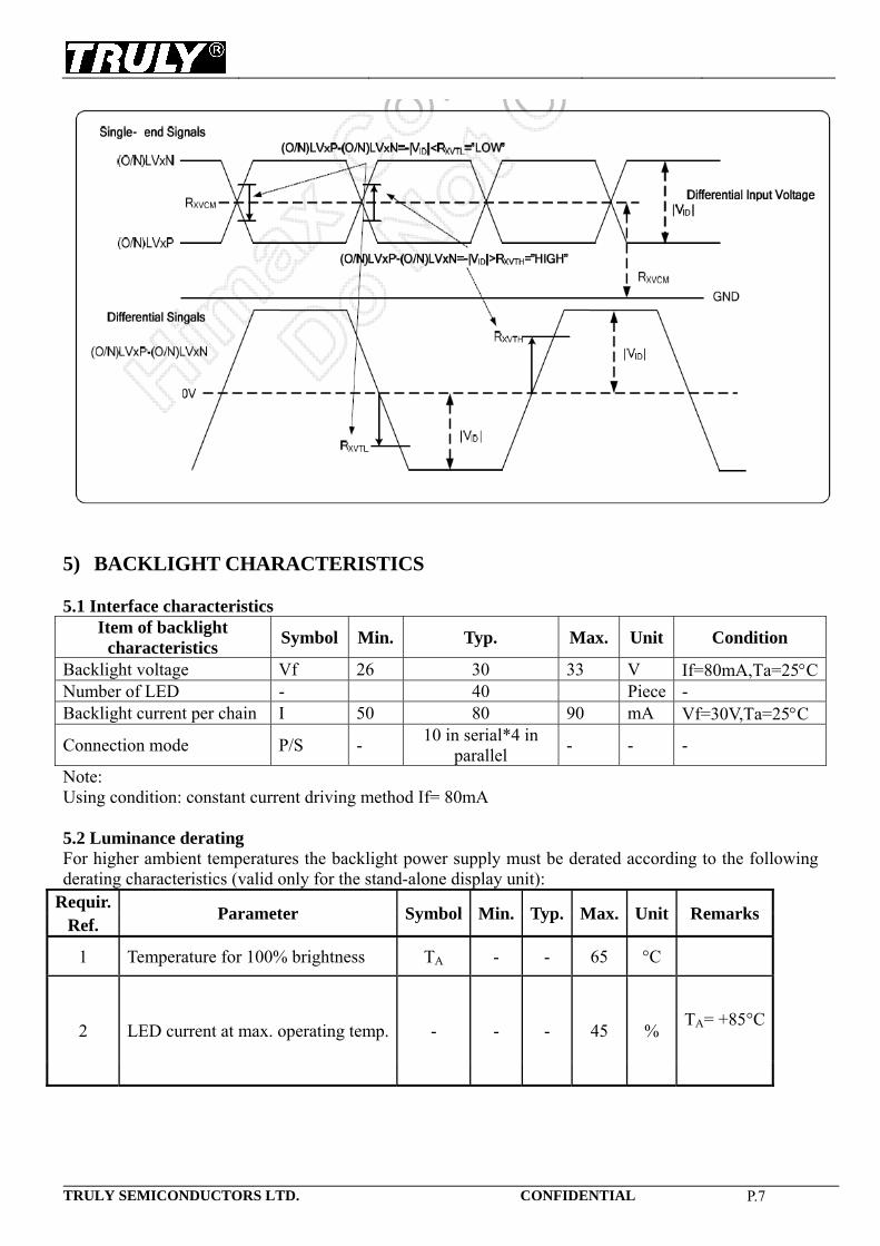
Supply voltage VCC 3.0 3.3 3.6 V Input Current(VCC=3.3) Idd - 410 500 mA Input voltage ' H ' level VIH 0.7VCC - VCC V Input voltage ' L ' level VIL GND - 0.3VCC V Output voltage ' H ' level VOH VCC-0.4 - - V Output voltage ' L ' level VOL GND - GND+0.4 V Operating frequency, per LVDS channel FLVDS 35 85 MHz Differential input high Threshold voltage*Note2,3 RXVTH - - +0.1 V Differential input low threshold voltage*Note2,3 RXVTL -0.1 - - V Differential input common Mode voltage*Note3 RXVCM 1 1.2 1.7-|VID|/2 V Differential input voltage*Note3 | VID | 0.2 0.6 V Differential input leakage Current*Note3 RVXliz -10 +10 uA *Note1: Test the input current of analog at the condition AVDD=3.3V type *Note2: RXVCM=1.2V *Note3
TRULY SEMICONDUCTORS LTD. CONFIDENTIAL P.7
5) BACKLIGHT CHARACTERISTICS 5.1 Interface characteristics
Item of backlight characteristics
Symbol Min. Typ. Max. Unit Condition
Backlight voltage Vf 26 30 33 V If=80mA,Ta=25CNumber of LED - 40 Piece - Backlight current per chain I 50 80 90 mA Vf=30V,Ta=25C
Connection mode P/S - 10 in serial*4 in
parallel - - -
Note: Using condition: constant current driving method If= 80mA 5.2 Luminance derating For higher ambient temperatures the backlight power supply must be derated according to the following derating characteristics (valid only for the stand-alone display unit):
Requir. Parameter Symbol Min. Typ. Max. Unit Remarks
Ref.
1 Temperature for 100% brightness TA - - 65 °C
2 LED current at max. operating temp. - - - 45 % TA= +85°C
TR
5.3 NC 5.3
5.3
Norefrel
RULY SEMIC
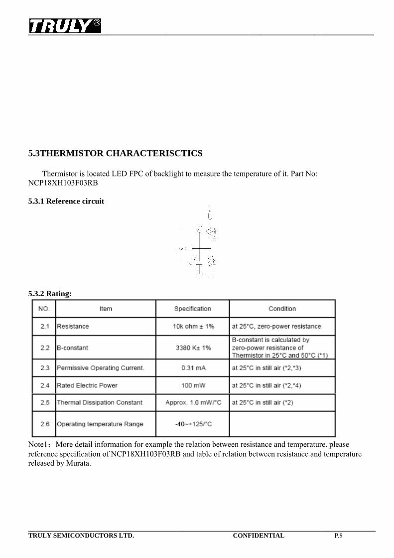
3THERM
ThermistoCP18XH10
3.1 Referen
3.2 Rating:
ote1:Moreference specleased by M
CONDUCTO
MISTOR C
or is located3F03RB
nce circuit
e detail infocification of
Murata.
ORS LTD.
CHARAC
d LED FPC
ormation forf NCP18XH
CTERISC
C of backligh
r example thH103F03RB
CTICS
ht to measu
he relation bB and table
CONF
ure the temp
between resof relation b
FIDENTIAL
perature of it
sistance andbetween res
t. Part No:
d temperatursistance and
P.8
re. please d temperaturre
TRULY SEMICONDUCTORS LTD. CONFIDENTIAL P.9
6) ELECTRO-OPTICAL CHARACTERISTICS
Item of electro-optical characteristics
Symbol Condition Min Typ Max Unit Remark Note
Response time Tr +Tf Ta=25C - 25 40 ms
FIG.1 1 Ta=-20C - 250 400 ms Ta=-30C - 650 800 ms
Contrast ratio Cr Ta=25C 700 900 - --- FIG 2. 2 Luminance uniformity white
Ta=25C. 75 85 - % FIG 2. 3
Luminance uniformity black 60 75 % FIG 2 3
Surface Luminance Lv Ta=25C. 700 1000 - cd/m2 FIG 2. 4
Viewing angle range (Cr>=10 @ 25C)
= 90 79 80 - deg FIG 3.
5 = 270 79 80 - deg FIG 3. = 0 79 80 - deg FIG 3. = 180 79 80 - deg FIG 3.
CIE (x, y) chromaticity
Red x
θ=0 =0 Ta=25C
0.603 0.633 0.663
/ FIG 2. 6
Red y 0.298 0.328 0.358 Green x 0.263 0.293 0.323 Green y 0.582 0.612 0.642 Blue x 0.120 0.150 0.180 Blue y 0.043 0.073 0.103 White x 0.240 0.280 0.320 White y 0.265 0.305 0.345
NTSC Ratio - θ=0 =0 Ta=25C
- 70 - %
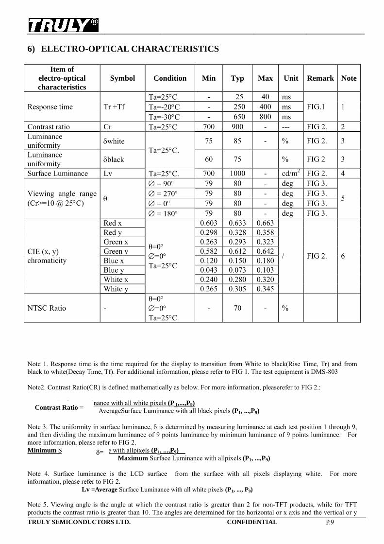
Note 1. Response time is the time required for the display to transition from White to black(Rise Time, Tr) and from black to white(Decay Time, Tf). For additional information, please refer to FIG 1. The test equipment is DMS-803 Note2. Contrast Ratio(CR) is defined mathematically as below. For more information, pleaserefer to FIG 2.:
AverageSurface Luminance with all white pixels (P 1,...,P9) AverageSurface Luminance with all black pixels (P1, ...,P9)
Note 3. The uniformity in surface luminance, is determined by measuring luminance at each test position 1 through 9, and then dividing the maximum luminance of 9 points luminance by minimum luminance of 9 points luminance. For more information, please refer to FIG 2. Minimum Surface Luminance with allpixels (P1, ...,P9)
Maximum Surface Luminance with allpixels (P1, ...,P9) Note 4. Surface luminance is the LCD surface from the surface with all pixels displaying white. For more information, please refer to FIG 2.
Lv =Average Surface Luminance with all white pixels (P1, ..., P9)
Note 5. Viewing angle is the angle at which the contrast ratio is greater than 2 for non-TFT products, while for TFT products the contrast ratio is greater than 10. The angles are determined for the horizontal or x axis and the vertical or y
=
Contrast Ratio =
TRULY SEMICONDUCTORS LTD. CONFIDENTIAL P.10
axis with respect to the z axis which is normal to the LCD surface. For more information, please refer to FIG 3. Note 6. For CIE (x, y) chromaticity, the x,y value is determined by measuring luminance at each test position 1 through 9,and then the average value is recorded.
FIG.1. The Definition of Response Time (E.g., Positive Product)
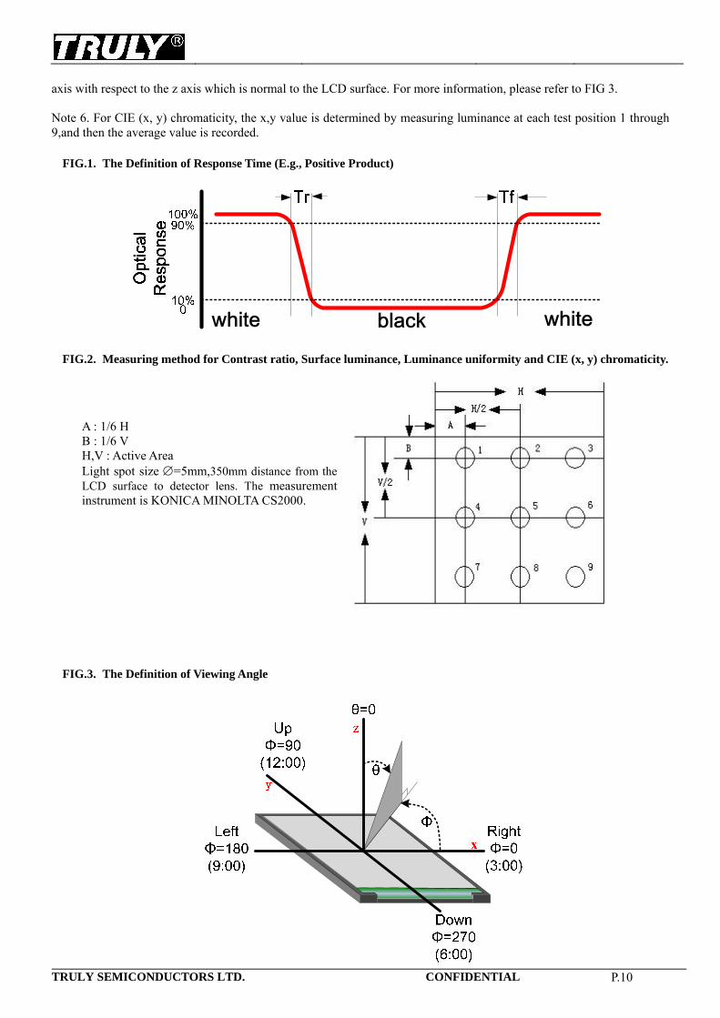
FIG.2. Measuring method for Contrast ratio, Surface luminance, Luminance uniformity and CIE (x, y) chromaticity.
FIG.3. The Definition of Viewing Angle
A : 1/6 H B : 1/6 V H,V : Active Area Light spot size =5mm,350mm distance from the LCD surface to detector lens. The measurement instrument is KONICA MINOLTA CS2000.
TRULY SEMICONDUCTORS LTD. CONFIDENTIAL P.11
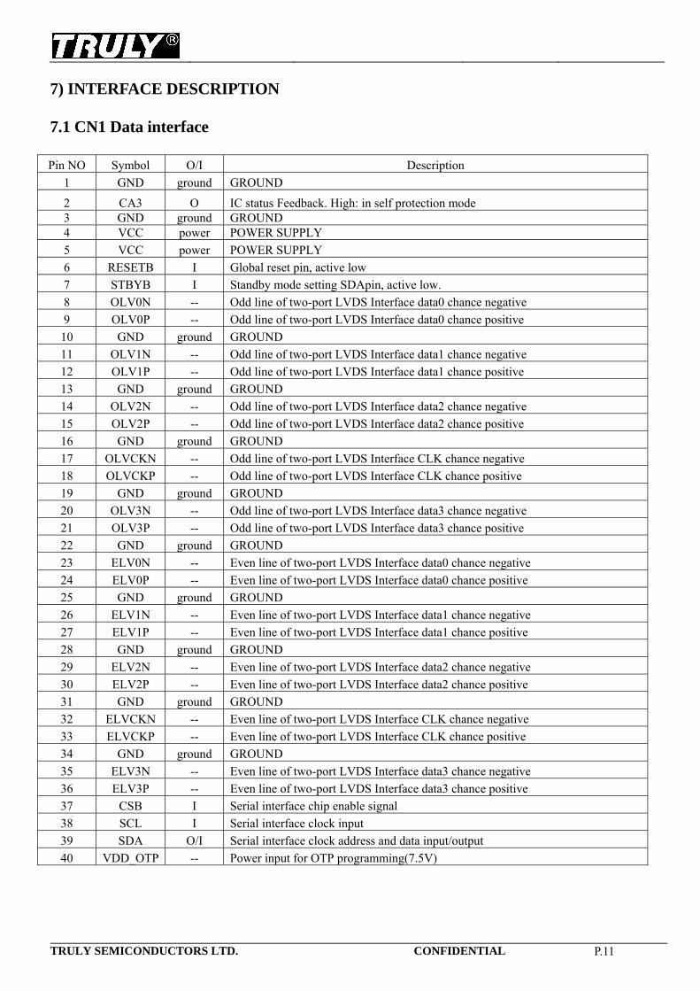
7) INTERFACE DESCRIPTION 7.1 CN1 Data interface Pin NO Symbol O/I Description
1 GND ground GROUND
2 CA3 O IC status Feedback. High: in self protection mode 3 GND ground GROUND 4 VCC power POWER SUPPLY
5 VCC power POWER SUPPLY
6 RESETB I Global reset pin, active low
7 STBYB I Standby mode setting SDApin, active low.
8 OLV0N -- Odd line of two-port LVDS Interface data0 chance negative
9 OLV0P -- Odd line of two-port LVDS Interface data0 chance positive
10 GND ground GROUND
11 OLV1N -- Odd line of two-port LVDS Interface data1 chance negative
12 OLV1P -- Odd line of two-port LVDS Interface data1 chance positive
13 GND ground GROUND
14 OLV2N -- Odd line of two-port LVDS Interface data2 chance negative
15 OLV2P -- Odd line of two-port LVDS Interface data2 chance positive
16 GND ground GROUND
17 OLVCKN -- Odd line of two-port LVDS Interface CLK chance negative
18 OLVCKP -- Odd line of two-port LVDS Interface CLK chance positive
19 GND ground GROUND
20 OLV3N -- Odd line of two-port LVDS Interface data3 chance negative
21 OLV3P -- Odd line of two-port LVDS Interface data3 chance positive
22 GND ground GROUND
23 ELV0N -- Even line of two-port LVDS Interface data0 chance negative
24 ELV0P -- Even line of two-port LVDS Interface data0 chance positive
25 GND ground GROUND
26 ELV1N -- Even line of two-port LVDS Interface data1 chance negative
27 ELV1P -- Even line of two-port LVDS Interface data1 chance positive
28 GND ground GROUND
29 ELV2N -- Even line of two-port LVDS Interface data2 chance negative
30 ELV2P -- Even line of two-port LVDS Interface data2 chance positive
31 GND ground GROUND
32 ELVCKN -- Even line of two-port LVDS Interface CLK chance negative
33 ELVCKP -- Even line of two-port LVDS Interface CLK chance positive
34 GND ground GROUND
35 ELV3N -- Even line of two-port LVDS Interface data3 chance negative
36 ELV3P -- Even line of two-port LVDS Interface data3 chance positive
37 CSB I Serial interface chip enable signal
38 SCL I Serial interface clock input
39 SDA O/I Serial interface clock address and data input/output
40 VDD_OTP -- Power input for OTP programming(7.5V)
TRULY SEMICONDUCTORS LTD. CONFIDENTIAL P.12
7.2 CN2 Backlight interface Pin NO Symbol O/I Description
1 LEDA1 power Backlight Anode 1
2 LEDA2 power Backlight Anode 2 3 LEDA3 power Backlight Anode 3 4 LEDA4 power Backlight Anode 4
5 NC -- Not connecting
6 LEDK1 power Backlight Cathode 1
7 LEDK2 power Backlight Cathode 2
8 LEDK3 power Backlight Cathode 3
9 LEDK4 power Backlight Cathode 4
10 NC -- Not connecting
11 NTC1 -- Thermistor Pin 1
12 NTC2 -- Thermistor Pin 2 8) TIMING CHARACTERISTICS
8.1 Power-On/OffSequence:
8.1.1 Power on timing sequence
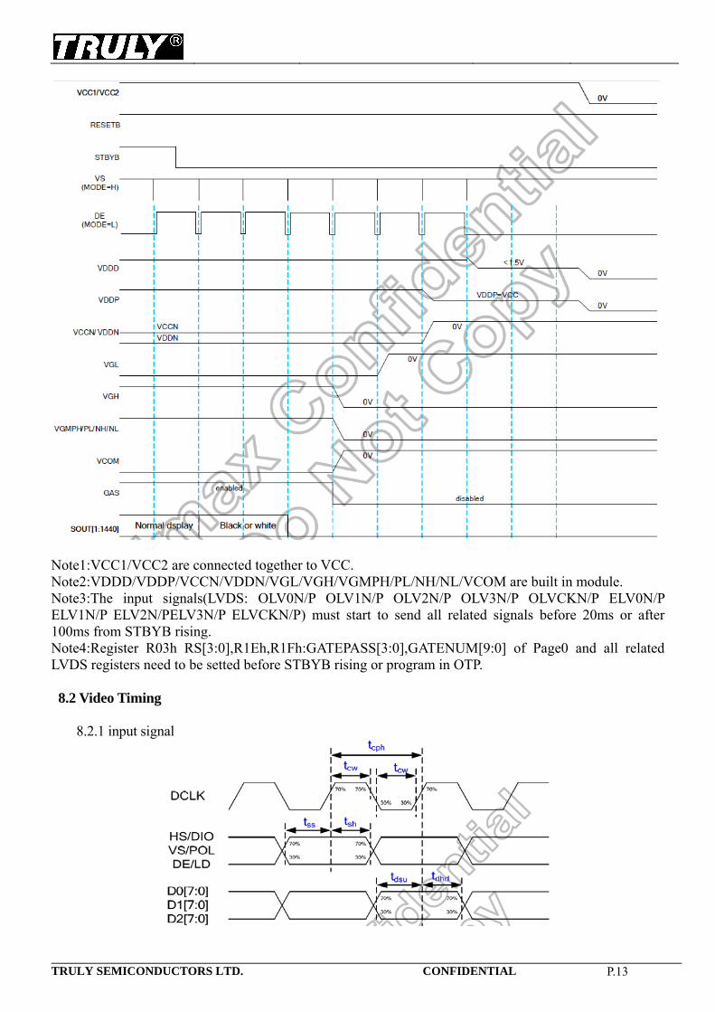
8.1.2power off timing sequence
TRULY SEMICONDUCTORS LTD. CONFIDENTIAL P.13
Note1:VCC1/VCC2 are connected together to VCC. Note2:VDDD/VDDP/VCCN/VDDN/VGL/VGH/VGMPH/PL/NH/NL/VCOM are built in module. Note3:The input signals(LVDS: OLV0N/P OLV1N/P OLV2N/P OLV3N/P OLVCKN/P ELV0N/P ELV1N/P ELV2N/PELV3N/P ELVCKN/P) must start to send all related signals before 20ms or after 100ms from STBYB rising. Note4:Register R03h RS[3:0],R1Eh,R1Fh:GATEPASS[3:0],GATENUM[9:0] of Page0 and all related LVDS registers need to be setted before STBYB rising or program in OTP. 8.2 Video Timing
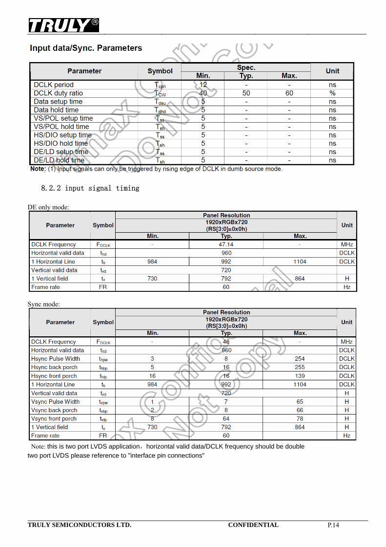
8.2.1 input signal
TRULY SEMICONDUCTORS LTD. CONFIDENTIAL P.14
8.2.2 input signal timing
DE only mode:
Sync mode:
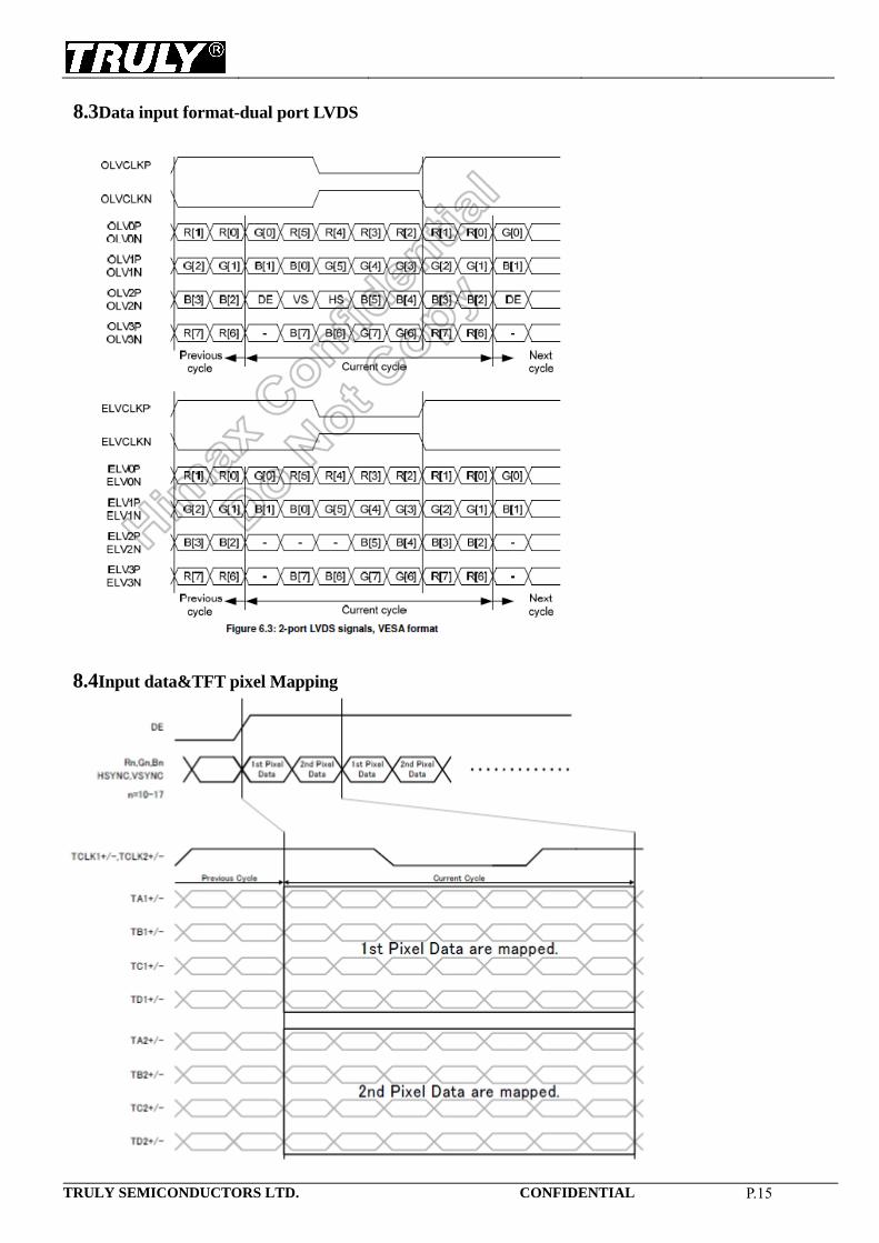
Note: this is two port LVDS application,horizontal valid data/DCLK frequency should be double
two port LVDS please reference to "interface pin connections"
TRULY SEMICONDUCTORS LTD. CONFIDENTIAL P.15
8.3Data input format-dual port LVDS
8.4Input data&TFT pixel Mapping
TRULY SEMICONDUCTORS LTD. CONFIDENTIAL P.16
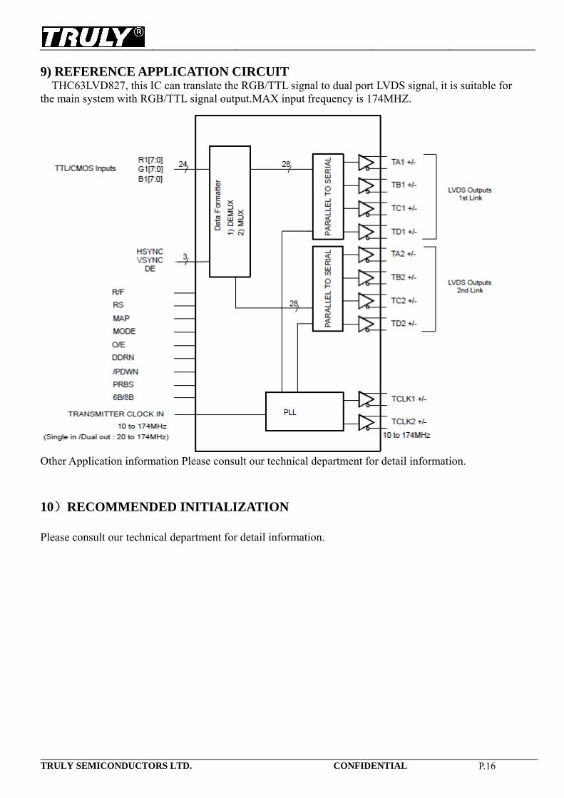
9) REFERENCE APPLICATION CIRCUIT THC63LVD827, this IC can translate the RGB/TTL signal to dual port LVDS signal, it is suitable for
the main system with RGB/TTL signal output.MAX input frequency is 174MHZ.
Other Application information Please consult our technical department for detail information. 10)RECOMMENDED INITIALIZATION Please consult our technical department for detail information.
TRULY SEMICONDUCTORS LTD. CONFIDENTIAL P.17
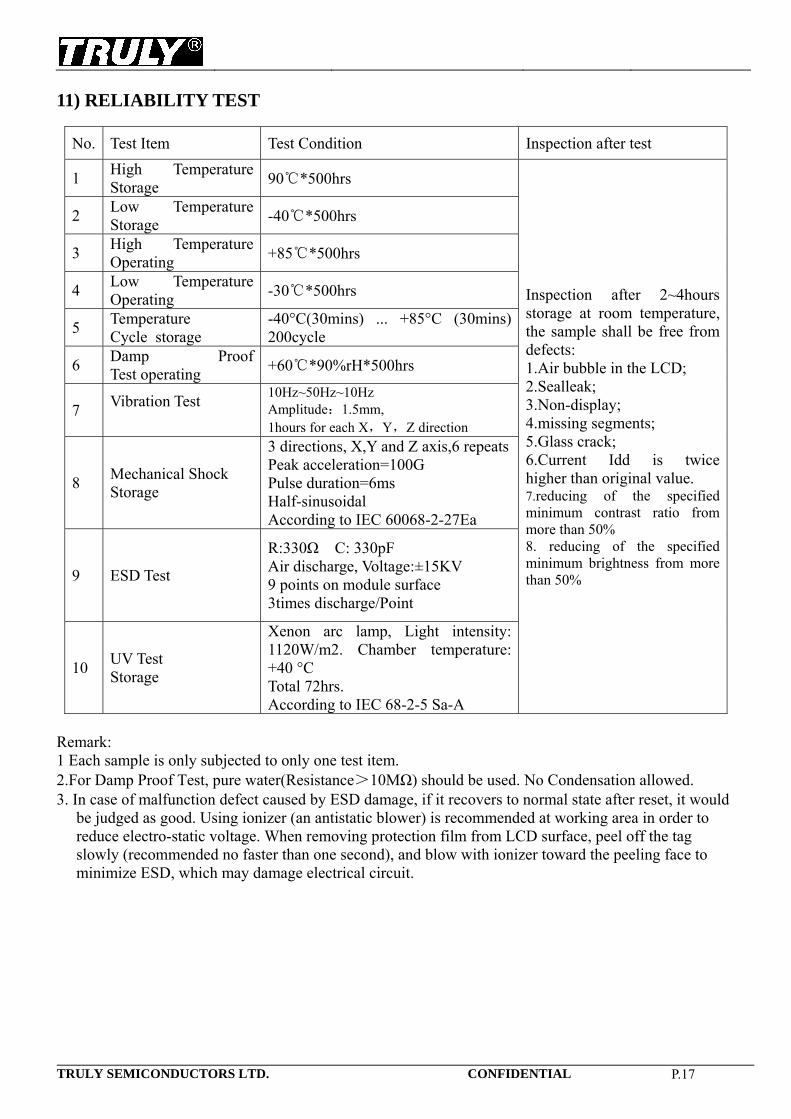
11) RELIABILITY TEST
No. Test Item Test Condition Inspection after test
1 High Temperature Storage
90*500hrs
Inspection after 2~4hours storage at room temperature, the sample shall be free from defects: 1.Air bubble in the LCD; 2.Sealleak; 3.Non-display; 4.missing segments; 5.Glass crack; 6.Current Idd is twice higher than original value. 7.reducing of the specified minimum contrast ratio from more than 50% 8. reducing of the specified minimum brightness from more than 50%
2 Low Temperature Storage
-40*500hrs
3 High Temperature Operating
+85*500hrs
4 Low Temperature Operating
-30*500hrs
5 Temperature Cycle storage
-40°C(30mins) ... +85°C (30mins) 200cycle
6 Damp Proof Test operating
+60*90%rH*500hrs
7 Vibration Test
10Hz~50Hz~10Hz Amplitude:1.5mm, 1hours for each X,Y,Z direction
8 Mechanical Shock Storage
3 directions, X,Y and Z axis,6 repeatsPeak acceleration=100G Pulse duration=6ms Half-sinusoidal According to IEC 60068-2-27Ea
9 ESD Test
R:330Ω C: 330pF Air discharge, Voltage:±15KV 9 points on module surface 3times discharge/Point
10 UV Test Storage
Xenon arc lamp, Light intensity: 1120W/m2. Chamber temperature: +40 °C Total 72hrs. According to IEC 68-2-5 Sa-A
Remark: 1 Each sample is only subjected to only one test item. 2.For Damp Proof Test, pure water(Resistance>10MΩ) should be used. No Condensation allowed. 3. In case of malfunction defect caused by ESD damage, if it recovers to normal state after reset, it would
be judged as good. Using ionizer (an antistatic blower) is recommended at working area in order to reduce electro-static voltage. When removing protection film from LCD surface, peel off the tag slowly (recommended no faster than one second), and blow with ionizer toward the peeling face to minimize ESD, which may damage electrical circuit.
TRULY SEMICONDUCTORS LTD. CONFIDENTIAL P.18
12) INSPECTION CRITERIA
ADD TFT Page 1 of 4
Outgoing Quality Standard TFT Product This specification is made to be used as the standard acceptance/rejection criteria for TFT Product.
1、Sample plan
Sampling plan according to GB/T2828.1-2003/ISO;1999 and ANSI/ASQCZ1.4-1993,normal level Ⅱ and based
on:
A non-conformance product:AQL0.65
B non-conformance product: AQL 1.5
2、Inspection condition
Viewing distance for cosmetic inspection is 20~30cm with bare eyes, and under an environment of
800lux~2000lux (20W~40W) light intensity, all directions for inspecting the sample should be within 45°against
perpendicular line. (Normal temperature 2025C and normal humidity 6015RH).
3、Definition
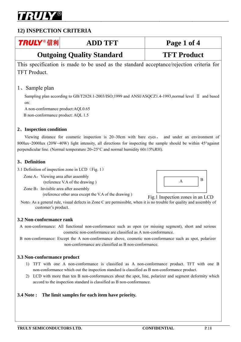
3.1 Definition of inspection zone in LCD(Fig. 1)
Zone A:Viewing area after assembly (reference V.A of the drawing )
Zone B:Invisible area after assembly (reference other area except the V.A of the drawing )
Note:As a general rule, visual defects in Zone C are permissible, when it is no trouble for quality and assembly of customer’s product.
3.2 Non-conformance rank A non-conformance: All functional non-conformance such as open (or missing segment), short and serious
cosmetic non-conformance are classified as A non-conformance.
B non-conformance: Except the A non-conformance above, cosmetic non-conformance such as spot, polarizer non-conformance are classified as B non-conformance.
3.3 Non-conformance product
1) TFT with one A non-conformance is classified as A non-conformance product. TFT with one B non-conformance which out the inspection standard is classified as B non-conformance product.
2) LCD with more than ten B non-conformances about the spot, line, polarizer and segment deformity which accord to the inspection standard is classified as B non-conformance.
3.4 Note : The limit samples for each item have priority.
BA
Fig.1 Inspection zones in an LCD
TRULY SEMICONDUCTORS LTD. CONFIDENTIAL P.19
ADD TFT Page 2 of 4
Outgoing Inspection Standard TFT Product
4、Inspection Standard
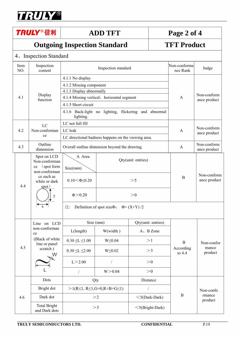
4.4
Spot on LCD Non-conformance (spot form non-conforman
ce such as white or dark
spot)
A Area Size(mm)
Qty(unit: entries)
B Non-conformance product0.10<Φ≤0.20 >5
Φ>0.20 >0
注: Definition of spot sizeΦ: Φ= (X+Y) /2
4.5
Line on LCD non-conformance (Black of white
line or panel scratch )
Size (mm) Qty(unit: entries)
B According
to 4.4
Non-conformance product
L(length) W(width ) A、B Zone
0.30 ≤L ≤1.00 W≤0.04 >1
0.30 ≤L ≤2.00 W≤0.02 >3
L>2.00 / >0
/ W>0.04 >0
4.6
Dots Qty Distance
B Non-confo
rmance product
Bright dot >1(R≤1, R≤1,G=0,R+B+G≤1) /
Dark dot >2 <5(Dark-Dark)
Total Bright and Dark dots
>3 <5(Bright-Dark)
Item NO.
Inspection content
Inspection standard Non-conforma
nce Rank Judge
4.1 Display function
4.1.1 No display
A Non-conformance product
4.1.2 Missing component
4.1.3 Display abnormally
4.1.4 Missing vertical,horizontal segment
4.1.5 Short circuit
4.1.6 Back-light no lighting, flickering and abnormal lighting.
4.2 LC
Non-conformance
LC not full fill
A Non-conformance product
LC leak
LC directional badness happens on the viewing area.
4.3 Outline
dimension Overall outline dimension beyond the drawing. A
Non-conformance product
y
x
TRULY SEMICONDUCTORS LTD. CONFIDENTIAL P.20
ADD TFT Page 3 of 4
Outgoing Inspection Standard TFT Product
4、Inspection Standard
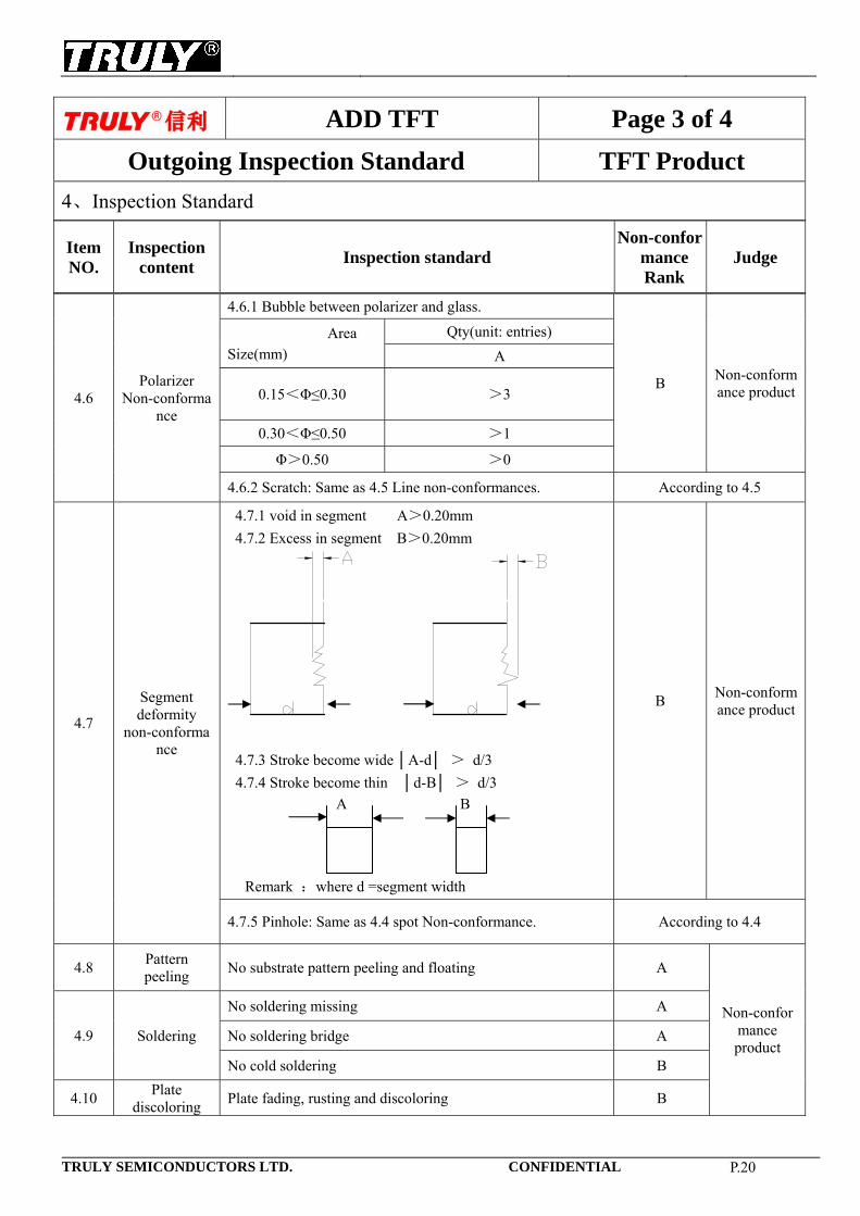
4.6 Polarizer
Non-conformance
4.6.1 Bubble between polarizer and glass.
B Non-conformance product
Area Size(mm)
Qty(unit: entries)
A
0.15<Φ≤0.30 >3
0.30<Φ≤0.50 >1
Φ>0.50 >0
4.6.2 Scratch: Same as 4.5 Line non-conformances. According to 4.5
4.7
Segment deformity
non-conformance
4.7.1 void in segment A>0.20mm
4.7.2 Excess in segment B>0.20mm
4.7.3 Stroke become wide A-d > d/3
4.7.4 Stroke become thin d-B > d/3
A B
Remark :where d =segment width
B Non-conformance product
4.7.5 Pinhole: Same as 4.4 spot Non-conformance. According to 4.4
4.8 Pattern peeling
No substrate pattern peeling and floating A
Non-conformance product
4.9 Soldering
No soldering missing A
No soldering bridge A
No cold soldering B
4.10 Plate
discoloring Plate fading, rusting and discoloring B
Item NO.
Inspection content
Inspection standard Non-confor
mance Rank
Judge
TRULY SEMICONDUCTORS LTD. CONFIDENTIAL P.21
ADD TFT Page 4 of 4
Outgoing Inspection Standard TFT Product
4、Inspection Standard
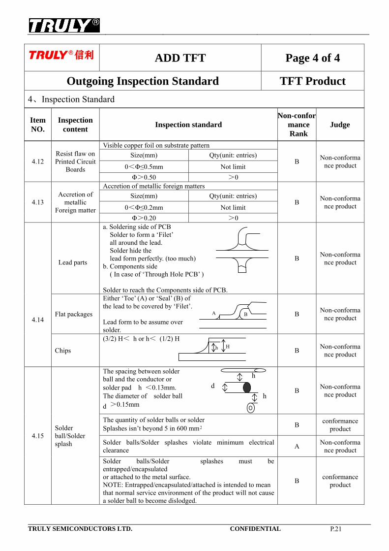
4.12 Resist flaw on Printed Circuit
Boards
Visible copper foil on substrate pattern
B Non-conforma
nce product
Size(mm) Qty(unit: entries)
0<Φ≤0.5mm Not limit
Φ>0.50 >0
4.13 Accretion of
metallic Foreign matter
Accretion of metallic foreign matters
B Non-conforma
nce product
Size(mm) Qty(unit: entries)
0<Φ≤0.2mm Not limit
Φ>0.20 >0
4.14
Lead parts
a. Soldering side of PCB Solder to form a ‘Filet’ all around the lead. Solder hide the lead form perfectly. (too much) b. Components side ( In case of ‘Through Hole PCB’ ) Solder to reach the Components side of PCB.
B Non-conforma
nce product
Flat packages
Either ‘Toe’ (A) or ‘Seal’ (B) of the lead to be covered by ‘Filet’. Lead form to be assume over solder.
B Non-conforma
nce product
Chips
(32) H< h or h< (12) H
B Non-conforma
nce product
4.15 Solder ball/Solder splash
The spacing between solder ball and the conductor or solder pad h <0.13mm. The diameter of solder ball
d >0.15mm
B Non-conforma
nce product
The quantity of solder balls or solder Splashes isn’t beyond 5 in 600 mm2
B conformance
product
Solder balls/Solder splashes violate minimum electrical clearance
A Non-conforma
nce product
Solder balls/Solder splashes must be entrapped/encapsulated or attached to the metal surface. NOTE: Entrapped/encapsulated/attached is intended to mean that normal service environment of the product will not cause a solder ball to become dislodged.
B conformance
product
Item NO.
Inspection content
Inspection standard Non-confor
mance Rank
Judge
A B
Hh
h
d
h
TRULY SEMICONDUCTORS LTD. CONFIDENTIAL P.22
13) PRECAUTIONS FOR USING LCD MODULES 1 Handling Precautions
1.1 The display product is quite sensitive to ESD. When handling it, you are advised to ensure
good grounding. The anti-ESD mat is recommended to keep the workbench free from electrical discharge; You are also reminded to remove the protective film a little slowly, the ESD may happen during this process.
1.2 To protect the FPC, heat seal or TCP, try to avoid touching the electrical components; Don’t over bend them, pull them or apply other external forces. The electrical connection might be damaged.
1.3 Customers are not advised to disassemble or rework the display products on their own. Switch off the power before operating on the display product. Connect or disconnect the electrical parts with power on might damage the product permanently.
1.4 Don’t scratch or push the polarizer with glass, tweezers or other parts with the hardness higher than HB. Don’t wipe the polarizer surface with chemically treated cloth, or cloth with oil.
1.5 If the display surface becomes contaminated, breathe on the surface and gently wipe it with a soft dry cloth. If it is heavily contaminated, moisten cloth with isopropyl alcohol(IPA) or ethyl alcohol. Do not use harmful chemicals such as ketone type materials, toluene, water, aromatic solvents to clean display’s surface.
1.6 Wipe off saliva, water or dew immediately, contact with water over a long period of time may cause deformation or color fading. Avoid contact with oil and fats.
1.7 Make sure the display product works on the recommended conditions, such as voltage, current and etc. with limited noise.
1.8 Customers are advised to follow the settings (initial codes) if provided. 1.9 Customer should consider the EMC standard when integrating the display product into a
system if there are such requirements. 1.10 Do not apply excessive force to the display surface or the adjoining areas since this may cause
the color tone to vary. Do not touch the display with bare hands. This will stain the display area and degrade insulation between terminals (some cosmetics are determined to the polarizer).
1.11 Please refer to the second parts for cartoons showing other details..
TRULY SEMICONDUCTORS LTD. CONFIDENTIAL P.23
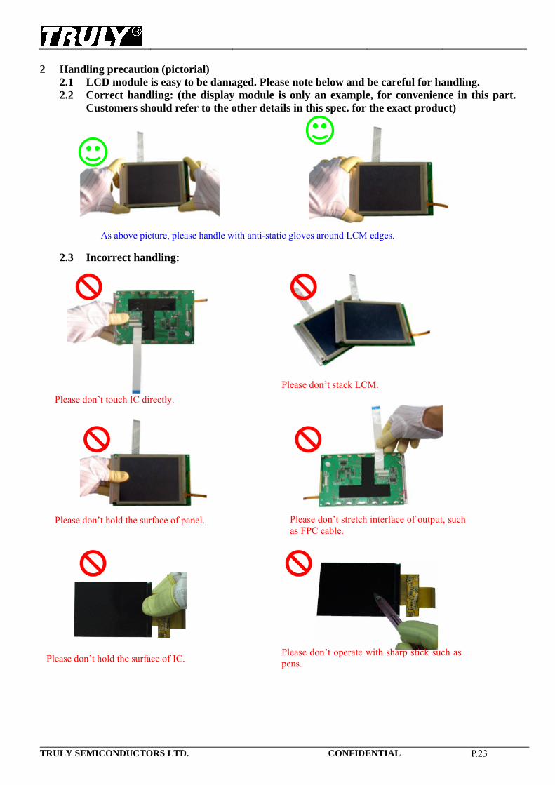
2 Handling precaution (pictorial) 2.1 LCD module is easy to be damaged. Please note below and be careful for handling. 2.2 Correct handling: (the display module is only an example, for convenience in this part.
Customers should refer to the other details in this spec. for the exact product)
2.3 Incorrect handling:
As above picture, please handle with anti-static gloves around LCM edges.
Please don’t hold the surface of panel.
Please don’t touch IC directly.
Please don’t stack LCM.
Please don’t operate with sharp stick such as pens.
Please don’t stretch interface of output, such as FPC cable.
Please don’t hold the surface of IC.
TRULY SEMICONDUCTORS LTD. CONFIDENTIAL P.24
3 Storage Precautions 3.1 Don’t put heavy loads on the display products. The polarizer should be kept away from other
goods. 3.2 Keep the display in a dark environment with relative humidity between 40%RH and
60%RHand temperature range between 5 to 35 C. Direct exposition to sunlight or other luminance is not allowed, especially UV light.
3.3 Don’t place the display product in any ambient with harmful air, acid, base or other oxidizing gases. Other chemical volatile solvents should be kept away.
4 Safety
4.1 The display product contains glass which breaks easily without care during handling. Don’t hurt yourself when glass is broken.
4.2 When the glass of the display product is broken, the liquid crystal may flow out. Please don’t inject it by yourself.
4.3 If any liquid leaks out of a damaged glass cell and comes in contact with the hands or skin, wash off thoroughly with soap and water.
4.4 If the liquid crystal gets into the eyes or mouth, please flush right away. Consult a doctor if necessary. 5 Others
5.1 Limited Warranty Unless agreed between TRULY and the customer, TRULY will replace or repair any of its
LCD modules which are found to be functionally defective when inspected in accordance with TRULY LCD acceptance standards (copies available upon request) for a period of one year from date of production. Cosmetic/visual defects must be returned to TRULY within 90 days of shipment. Confirmation of such date shall be based on data code on product. The warranty liability of TRULY limited to repair and/or replace on the terms set forth above. TRULY will not be responsible for any subsequent or consequential events.
5.2 Return LCM under warranty
5.2.1 No warranty can be granted if the precautions stated above have been disregarded. The typical examples of violations are :
5.2.1.1 - Broken LCD glass.
5.2.1.2 - PCB eyelet is damaged or modified.
5.2.1.3 -PCB conductors damaged.
5.2.1.4 - Circuit modified in any way, including addition of components.
5.2.1.5 - PCB tampered with by grinding, engraving or painting varnish.
5.2.1.6 - Soldering to or modifying the bezel in any manner.
5.2.2 Module repairs will be invoiced to the customer upon mutual agreement. Modules must be
returned with sufficient description of the failures or defects. Any connectors or cable
installed by the customer must be removed completely without damaging the PCB eyelet,
conductors and terminals.
14) PACKING SPECIFICATION
Please consult our technical department for detail information.
TRULY SEMICONDUCTORS LTD. CONFIDENTIAL P.25
FACTORY CONTACT INFORMATION FACTORY NAME: TRULY SEMICONDUCTORS LTD. FACTORY ADDRESS: Truly Industrial Area, ShanWei City,GuangDong,China P.C: 516600 URL: http://www.truly.com.hk http://www.trulysemi.com
Related Documents